M.Sc. Thesis - CiteSeerX
119
Faculty of Electrical Engineering, Mathematics and Computer Science Circuits and Systems Mekelweg 4, 2628 CD Delft The Netherlands http://ens.ewi.tudelft.nl/ CAS-MS-2010-05 M.Sc. Thesis Standard Cell Behavior Analysis and Waveform Set Model for Statistical Static Timing Analysis Ashish Nigam Abstract As we are moving toward nanometre technology, the variability in the circuit parameters and operating environment (Process, Voltage and Temperature (PVT) ) are increasing, causing uncertainty in the circuit performance. Statistical Static Timing Analysis (SSTA) is a category of methodologies to analyse the variations in delay due to PVT variations. This thesis work is a part of the MODERN project, which is involved in developing a new SSTA methodology. In this thesis, the variation of the delay in 45nm standard cells is analysed. In industry practice, the Monte Carlo method is often used to estimate the statistical moments. This method needs a large number of simulation iterations and these simulations are parameter distribution dependent. A fast statistical moment estimation method is proposed in this work. The proposed methodology is at least 100× faster than the Monte Carlo method and simulations are independent of the parameter distribution. In the SSTA methodology of the MODERN project, the signal waveforms with their variations are preserved at each pin of the stan- dard cell. The concept of a “set of waveforms” as a representation of a variable electrical signal is also developed in this thesis work. Pos- sible methods to represent the set of waveforms and their integration with the timing analysis methodology are analysed. The pseudo cir- cuit based representation turns out to be the most compact model. A methodology for the analysis of the accuracy and efficiency of the pseudo circuit model is proposed.
-
Upload
khangminh22 -
Category
Documents
-
view
0 -
download
0
Transcript of M.Sc. Thesis - CiteSeerX

Faculty of Electrical Engineering, Mathematics and Computer Science
Circuits and SystemsMekelweg 4,
2628 CD DelftThe Netherlands
http://ens.ewi.tudelft.nl/
CAS-MS-2010-05
M.Sc. Thesis
Standard Cell Behavior Analysis and
Waveform Set Model for Statistical Static
Timing Analysis
Ashish Nigam
Abstract
As we are moving toward nanometre technology, the variability inthe circuit parameters and operating environment (Process, Voltageand Temperature (PVT)) are increasing, causing uncertainty in thecircuit performance. Statistical Static Timing Analysis (SSTA) is acategory of methodologies to analyse the variations in delay due toPVT variations. This thesis work is a part of the MODERN project,which is involved in developing a new SSTA methodology.
In this thesis, the variation of the delay in 45nm standard cellsis analysed. In industry practice, the Monte Carlo method is oftenused to estimate the statistical moments. This method needs a largenumber of simulation iterations and these simulations are parameterdistribution dependent. A fast statistical moment estimation methodis proposed in this work. The proposed methodology is at least 100×faster than the Monte Carlo method and simulations are independentof the parameter distribution.
In the SSTA methodology of the MODERN project, the signalwaveforms with their variations are preserved at each pin of the stan-dard cell. The concept of a “set of waveforms” as a representation ofa variable electrical signal is also developed in this thesis work. Pos-sible methods to represent the set of waveforms and their integrationwith the timing analysis methodology are analysed. The pseudo cir-cuit based representation turns out to be the most compact model.A methodology for the analysis of the accuracy and efficiency of thepseudo circuit model is proposed.


Standard Cell Behavior Analysis and Waveform Set
Model for Statistical Static Timing Analysis
Thesis
submitted in partial fulfillment of therequirements for the degree of
Master of Science
in
Microelectronics
by
Ashish Nigamborn in Tulsipur, India
This work was performed in:
Circuits and Systems GroupDepartment of Microelectronics & Computer EngineeringFaculty of Electrical Engineering, Mathematics and Computer ScienceDelft University of Technology

Delft University of Technology
Copyright c© 2010 Circuits and Systems GroupAll rights reserved.

Delft University of Technology
Department of
Microelectronics & Computer Engineering
The undersigned hereby certify that they have read and recommend to the Facultyof Electrical Engineering, Mathematics and Computer Science for acceptance a thesisentitled “Standard Cell Behavior Analysis and Waveform Set Model for Sta-
tistical Static Timing Analysis” by Ashish Nigam in partial fulfillment of therequirements for the degree of Master of Science.
Dated: 30 June 2010
Chairman:prof. dr. ir. Edoardo Charbon
Advisors:dr. ir. Nick van der Meijs
dr. ir. Michel Berkelaar
Committee Members:dr. ir. Said Hamdioui

iv
Abstract
As we are moving toward nanometre technology, the variability in the circuit parame-ters and operating environment (Process, Voltage and Temperature (PVT)) are increas-ing, causing uncertainty in the circuit performance. Statistical Static Timing Analysis(SSTA) is a category of methodologies to analyse the variations in delay due to PVTvariations. This thesis work is a part of the MODERN project, which is involved indeveloping a new SSTA methodology.
In this thesis, the variation of the delay in 45nm standard cells is analysed. In indus-try practice, the Monte Carlo method is often used to estimate the statistical moments.This method needs a large number of simulation iterations and these simulations areparameter distribution dependent. A fast statistical moment estimation method is pro-posed in this work. The proposed methodology is at least 100× faster than the MonteCarlo method and simulations are independent of the parameter distribution.
In the SSTA methodology of the MODERN project, the signal waveforms with theirvariations are preserved at each pin of the standard cell. The concept of a “set of wave-forms” as a representation of a variable electrical signal is also developed in this thesiswork. Possible methods to represent the set of waveforms and their integration withthe timing analysis methodology are analysed. The pseudo circuit based representa-tion turns out to be the most compact model. A methodology for the analysis of theaccuracy and efficiency of the pseudo circuit model is proposed.
v

vi

Acknowledgments
First and foremost I offer my sincerest gratitude to my supervisors dr. ir. Nick vander Meijs and dr. ir. Michel Berkelaar who have supported me throughout my thesis.They guided me towards the right direction at every difficult time during my thesisproject. I attribute the level of my Masters degree to their encouragement and effortand without them this thesis, too, would not have been completed or written. I wouldalso like to sincerely thank the other members of the MODERN project, Qin Tang,Amir Zjajo, and Kees-Jan van der Kolk. They spent many discussion hours to listen tomy ideas and gave their feedback to improve the quality of work. They all encouragedand helped me to write the paper and supported to improve my thesis report. Onesimply could not wish for a better or friendlier supervisor and research group.
I would also like to thank prof. Alessandro Di Bucchianico, Eindhoven Univer-sity of Technology, for useful discussions and contributions. His help in reviewing themathematical models of the thesis work was a great help.
I would like to thank prof. dr. ir. Edoardo Charbon and dr. ir. Said Hamdioui fortheir valuable time spent in my thesis defence committee.
Antoon Frehe has provided me all kind of support for the compute machines andsoftware which are critical in compute intensive thesis work. Laura Bruns and JudithBukman-Vollering have helped me in all the office related work, which saved significanttime and effort.
In my daily work I have been blessed with a friendly and cheerful group of fellowstudents. Chokalingam Veerappan, Saket Sakunia, Akansh Goyal, Shahzad Gishkori,and Maxim Volkov have helped me to develop and refine the methodology I used in mythesis work. Their healthy discussions and valuable feedback solved various problemsof mine. There are many other friends in Delft who made my life filled with joy duringmy two years masters program. I sincerely thank all of them, without them life wouldnot have been possible in Delft.
Finally, I thank my parents for supporting me throughout my studies at Delft Uni-versity of Technology.
Ashish NigamDelft, The Netherlands30 June 2010
vii

viii

Contents
Abstract v
Acknowledgments vii
List of Abbreviations xv
1 Introduction 1
1.1 Motivation . . . . . . . . . . . . . . . . . . . . . . . . . . . . . . . . . . 11.2 Project Sketch . . . . . . . . . . . . . . . . . . . . . . . . . . . . . . . . 11.3 Thesis Overview . . . . . . . . . . . . . . . . . . . . . . . . . . . . . . . 2
2 Digital Circuit and PVT Variations 3
2.1 Digital Circuit . . . . . . . . . . . . . . . . . . . . . . . . . . . . . . . . 42.2 Static Timing Analysis . . . . . . . . . . . . . . . . . . . . . . . . . . . 9
2.2.1 Non-linear Delay Model . . . . . . . . . . . . . . . . . . . . . . 122.2.2 Composite Current Source Model . . . . . . . . . . . . . . . . . 122.2.3 Effective Current Source Model . . . . . . . . . . . . . . . . . . 13
2.3 Statistical Static Timing Analysis . . . . . . . . . . . . . . . . . . . . . 142.4 Circuit Simulation and Analysis Environment . . . . . . . . . . . . . . 152.5 Summary . . . . . . . . . . . . . . . . . . . . . . . . . . . . . . . . . . 16
3 Delay Variations 17
3.1 Variations in the PVT parameters . . . . . . . . . . . . . . . . . . . . . 173.2 Circuit Simulation Configuration . . . . . . . . . . . . . . . . . . . . . 203.3 Delay variation in an inverter . . . . . . . . . . . . . . . . . . . . . . . 22
3.3.1 Individual Parameter Variation . . . . . . . . . . . . . . . . . . 243.3.2 Combination of two parameters variations . . . . . . . . . . . . 263.3.3 A realistic PVT variation . . . . . . . . . . . . . . . . . . . . . 28
3.4 Higher order statistical moments . . . . . . . . . . . . . . . . . . . . . 293.5 Delay variation in various standard cells . . . . . . . . . . . . . . . . . 303.6 Summary . . . . . . . . . . . . . . . . . . . . . . . . . . . . . . . . . . 33
4 Statistical Moment Estimation and Probability Density Function 35
4.1 Motivation . . . . . . . . . . . . . . . . . . . . . . . . . . . . . . . . . . 354.2 Fast Statistical Moment Estimation Method . . . . . . . . . . . . . . . 36
4.2.1 Circuit Simulation . . . . . . . . . . . . . . . . . . . . . . . . . 374.2.2 Data Processing . . . . . . . . . . . . . . . . . . . . . . . . . . . 37
4.3 Simulation Results and Comparison for FSME Method . . . . . . . . . 424.4 Probability Density Function Estimation Method . . . . . . . . . . . . 48
4.4.1 PDF Estimation - Bin Method . . . . . . . . . . . . . . . . . . . 504.4.2 PDF Estimation - Direct Method . . . . . . . . . . . . . . . . . 51
4.5 Simulation Results for PDF Estimation Method . . . . . . . . . . . . . 51
ix

4.6 Summary . . . . . . . . . . . . . . . . . . . . . . . . . . . . . . . . . . 52
5 The Set of Waveforms 55
5.1 Concept of a Set of Waveforms . . . . . . . . . . . . . . . . . . . . . . 555.2 Representing Uncertainty with the Set of Waveforms . . . . . . . . . . 575.3 Representation of the Set of Waveforms . . . . . . . . . . . . . . . . . . 59
5.3.1 Lookup Table based Representation . . . . . . . . . . . . . . . . 605.3.2 Statistical Moments based Representation . . . . . . . . . . . . 605.3.3 Pseudo Circuit based Representation . . . . . . . . . . . . . . . 63
5.4 Comparison of various Waveform Set Representations . . . . . . . . . . 655.5 Summary . . . . . . . . . . . . . . . . . . . . . . . . . . . . . . . . . . 65
6 Pseudo Circuit Model 67
6.1 Pseudo Circuit, Waveform Set and SSTA Engine . . . . . . . . . . . . . 676.2 The Pseudo Circuit Model . . . . . . . . . . . . . . . . . . . . . . . . . 67
6.2.1 The Pseudo Circuit . . . . . . . . . . . . . . . . . . . . . . . . . 686.2.2 Database processing for waveform comparison . . . . . . . . . . 72
6.3 Waveform Comparison Methodology . . . . . . . . . . . . . . . . . . . 766.4 Results . . . . . . . . . . . . . . . . . . . . . . . . . . . . . . . . . . . . 836.5 Summary . . . . . . . . . . . . . . . . . . . . . . . . . . . . . . . . . . 85
7 Conclusion 87
7.1 Summary . . . . . . . . . . . . . . . . . . . . . . . . . . . . . . . . . . 877.2 Future Work . . . . . . . . . . . . . . . . . . . . . . . . . . . . . . . . . 88
A Delay Variations 89
Bibliography 97
List of Publications 101
x

List of Figures
2.1 Full-custom design and semi-custom design . . . . . . . . . . . . . . . . 32.2 Data Path . . . . . . . . . . . . . . . . . . . . . . . . . . . . . . . . . . 52.3 Slew . . . . . . . . . . . . . . . . . . . . . . . . . . . . . . . . . . . . . 52.4 Illustration of a circuit component delay . . . . . . . . . . . . . . . . . 62.5 Master-Slave DFF with MUX . . . . . . . . . . . . . . . . . . . . . . . 72.6 Master-Slave DFF with MUX as Pass Transistor Logic . . . . . . . . . 72.7 Setup, Hold, and Clock to Q Delay in Waveform . . . . . . . . . . . . . 82.8 DFF to DFF Path . . . . . . . . . . . . . . . . . . . . . . . . . . . . . 92.9 Path Delay . . . . . . . . . . . . . . . . . . . . . . . . . . . . . . . . . 92.10 CMOS Inverter . . . . . . . . . . . . . . . . . . . . . . . . . . . . . . . 102.11 ON and OFF state of the PMOS and the NMOS in an Inverter . . . . 112.12 Measurement of Iout(t) for a set of Sin and Cout . . . . . . . . . . . . . 132.13 Measurement of Vout(t) for a set of Sin and Cout . . . . . . . . . . . . . 14
3.1 Spread estimation for PTM Model . . . . . . . . . . . . . . . . . . . . 193.2 Delay of INV X1 vs W for µW = 90nm and 3σW = 58nm . . . . . . . . 213.3 INV X1 simulation configuration . . . . . . . . . . . . . . . . . . . . . 233.4 Delay variation due to L . . . . . . . . . . . . . . . . . . . . . . . . . . 253.5 Delay variation due to W & L . . . . . . . . . . . . . . . . . . . . . . . 273.6 Delay distribution pdf due to realistic PVT variations . . . . . . . . . . 29
4.1 Numerical Integration Method . . . . . . . . . . . . . . . . . . . . . . 394.2 Piecewise constant approximation of probability density function . . . . 404.3 The first four moment estimation vs simulation runs for MC and FSME
with one parameter (L) and two parameters (L and W ) variations in45nm Inverter . . . . . . . . . . . . . . . . . . . . . . . . . . . . . . . . 44
4.4 The first four moment estimation vs simulation runs for MC and FSMEwith one parameter (L) and two parameters (L and W ) variations in32nm Inverter . . . . . . . . . . . . . . . . . . . . . . . . . . . . . . . . 45
4.5 Moment estimation vs simulation run in 45nm inverter chain using Gaus-sian (N), Lognormal (L), Gamma (G), and Beta (B) distributions. . . . 48
4.6 Moment estimation vs simulation run in 45nm inverter chain using Gaus-sian (N), Lognormal (L), Gamma (G), and Beta (B) distributions withRelative Scale. . . . . . . . . . . . . . . . . . . . . . . . . . . . . . . . . 49
4.7 pdf of the delay of an 45nm inverter chain using Gaussian (N), Lognormal(L), Gamma (G), and Beta (B) distributions. . . . . . . . . . . . . . . 52
4.8 pdf of the delay of an 45nm inverter chain using Gaussian (N), Lognormal(L), Gamma (G), and Beta (B) distributions in one plot . . . . . . . . 53
5.1 A Inverter for Waveform Set . . . . . . . . . . . . . . . . . . . . . . . . 575.2 The Set of Waveforms for Inverter . . . . . . . . . . . . . . . . . . . . . 585.3 A Inverter Chain for Waveform Set . . . . . . . . . . . . . . . . . . . . 585.4 The Set of Waveforms for Inverter Chain . . . . . . . . . . . . . . . . . 59
xi

5.5 SSTA Engine . . . . . . . . . . . . . . . . . . . . . . . . . . . . . . . . 595.6 SSTA Engine with Table Model . . . . . . . . . . . . . . . . . . . . . . 605.7 Vertical cross-section of Waveforms at time t . . . . . . . . . . . . . . . 615.8 Vertical cross-section of Waveforms at time t with µ and ±σ of voltage 625.9 First four moments of the waveform set as a function of time . . . . . . 635.10 SSTA Engine with Moment Model . . . . . . . . . . . . . . . . . . . . 645.11 Example path for SSTA . . . . . . . . . . . . . . . . . . . . . . . . . . 645.12 SSTA Engine with Pseudo Circuit Model . . . . . . . . . . . . . . . . . 65
6.1 An inverter chain with three inverters . . . . . . . . . . . . . . . . . . . 686.2 Inverter chain with input source and output load . . . . . . . . . . . . 696.3 Inverter chain with capacitors at internal nodes . . . . . . . . . . . . . 706.4 Inverter chain with time offset . . . . . . . . . . . . . . . . . . . . . . . 706.5 The Pseudo Circuit Schematic . . . . . . . . . . . . . . . . . . . . . . . 716.6 Quality factors for the waveform comparison . . . . . . . . . . . . . . . 736.7 Target Waveform Set . . . . . . . . . . . . . . . . . . . . . . . . . . . . 786.8 Sin vs Cload intersaction line for QSlew equals to TSlew . . . . . . . . . . 796.9 Sin vs Cload intersaction line for QShiftMean equals to QShiftMean . . . . 806.10 Intersection of Slew and ShiftMean lines . . . . . . . . . . . . . . . . . 816.11 QMax vs σL . . . . . . . . . . . . . . . . . . . . . . . . . . . . . . . . . 826.12 Comparison of pseudo circuit model and target set of waveforms . . . . 846.13 Result comparison of pseudo circuit model and target waveform set . . 85
A.1 Delay variation due to L . . . . . . . . . . . . . . . . . . . . . . . . . . 89A.2 Delay variation due to W . . . . . . . . . . . . . . . . . . . . . . . . . 89A.3 Delay variation due to Vth . . . . . . . . . . . . . . . . . . . . . . . . . 90A.4 Delay variation due to VDD . . . . . . . . . . . . . . . . . . . . . . . . 90A.5 Delay variation due to T . . . . . . . . . . . . . . . . . . . . . . . . . . 91A.6 Delay variation due to VDD & T . . . . . . . . . . . . . . . . . . . . . . 91A.7 Delay variation due to VDD & Vth . . . . . . . . . . . . . . . . . . . . . 92A.8 Delay variation due to VDD & W . . . . . . . . . . . . . . . . . . . . . 92A.9 Delay variation due to VDD & L . . . . . . . . . . . . . . . . . . . . . . 93A.10 Delay variation due to T & Vth . . . . . . . . . . . . . . . . . . . . . . 93A.11 Delay variation due to T & W . . . . . . . . . . . . . . . . . . . . . . . 94A.12 Delay variation due to T & L . . . . . . . . . . . . . . . . . . . . . . . 94A.13 Delay variation due to Vth & W . . . . . . . . . . . . . . . . . . . . . . 95A.14 Delay variation due to Vth & L . . . . . . . . . . . . . . . . . . . . . . 95A.15 Delay variation due to W & L . . . . . . . . . . . . . . . . . . . . . . . 96A.16 Delay distribution pdf for a realistic PVT variations . . . . . . . . . . . 96
xii

List of Tables
2.1 NLDM based cell delay (tdelay) lookup table . . . . . . . . . . . . . . . 122.2 CCS based output current waveform (Iout(t)) lookup table . . . . . . . 132.3 ECSM based output voltage waveform (Vout(t)) lookup table . . . . . . 13
3.1 Technology process parameter trends based on [3] . . . . . . . . . . . . 183.2 Spread of the PVT parameters . . . . . . . . . . . . . . . . . . . . . . . 203.3 Nominal and 3σ range for Nangate INV X1 inverter . . . . . . . . . . . 213.4 Nominal and 3σ range for modified INV X1 inverter . . . . . . . . . . . 223.5 INV X1 simulation configuration . . . . . . . . . . . . . . . . . . . . . 233.6 Delay spread of INV X1 due to individual parameter variation . . . . . 243.7 Delay variation due to two parameter variations . . . . . . . . . . . . . 283.8 Delay variation due to realistic PVT variation . . . . . . . . . . . . . . 293.9 First four statistical moments of delay variation in INV X1 due to real-
istic PVT variation . . . . . . . . . . . . . . . . . . . . . . . . . . . . . 303.10 List of standard cells . . . . . . . . . . . . . . . . . . . . . . . . . . . . 313.11 Delay variation in Nangate standard cells (INV, NAND2, and NOR2)
due to realistic PVT variation . . . . . . . . . . . . . . . . . . . . . . . 323.12 Delay variation in Nangate standard cells (BUF, AND2, OR2, XOR2
and XNOR2) due to realistic PVT variation . . . . . . . . . . . . . . . 33
4.1 Error % comparison in the first four moments estimation of delay for oneparameter (L) variation using Monte Carlo (5000 runs) and the proposedmethod (50 runs) in 45nm and 32nm PTM technologies . . . . . . . . . 46
4.2 Error % comparison in the first four moments estimation of delay fortwo parameters (L and W ) variation using Monte Carlo (10000 runs)and the proposed method (100 runs) in 45nm and 32nm PTM technologies 47
6.1 The Pseudo Circuit . . . . . . . . . . . . . . . . . . . . . . . . . . . . . 716.2 Pseudo Circuit Parameters . . . . . . . . . . . . . . . . . . . . . . . . . 716.3 Simulation output in database . . . . . . . . . . . . . . . . . . . . . . . 726.4 Mean and SD curves for quality factor illustration . . . . . . . . . . . . 736.5 Database Structure . . . . . . . . . . . . . . . . . . . . . . . . . . . . . 766.6 Quality factors of target waveform . . . . . . . . . . . . . . . . . . . . . 776.7 Pseudo Circuit Parameters after waveform comparison methodology . . 836.8 Quality factors of target waveform set and pseudo circuit model . . . . 84
xiii

xiv
List of Abbreviations
ASIC Application Specific Integrated Circuits
BSIM Berkeley Short-channel IGFET Model
CCS Composite Current Source Model
CMOS Complementary Metal Oxide Semiconductor
DFF Edge Triggered Flip-Flop
ECSM Effective Current Source Model
EKV Transistor Model given by C. C. Enz, F. Krummenacher and E. A. Vittoz
EPFL Ecole Polytechnique Federale de Lausanne
FSME Fast Statistical Moment Estimation Method
HP High Performance
IC Integrated Circuits
ITRS International Technology Roadmap for Semiconductor
LHS Latin Hypercube Sampling
LP Low Power
MC Monte Carlo
MODERN MOdeling and DEsign of Reliable, process variation-aware Nanoelec-tronic devices, circuits and systems
MOSFET Metal Oxide Semiconductor Field Effect Transistors
MUX Multiplexer
NLDM Non-Linear Delay Model
NMOS n-type Metal Oxide Semiconductor Field Effect Transistors
PCA Principal Component Analysis
PDF Probability Density Function
PMOS p-type Metal Oxide Semiconductor Field Effect Transistors
PTM Predictive Technology Model
PVT Process, Voltage and Temperature
PWC Piecewise Constant
QMC Quasi Monte Carlo
SH-QMC Stratification + Hybrid Quasi Monte Carlo
SPICE Simulation Program with Integrated Circuit Emphasis
SSTA Statistical Static Timing Analysis
STA Static Timing Analysis
UCB University of California, Berkeley
xv

xvi

Introduction 11.1 Motivation
Economical benefit is the main driving force for shrinking of CMOS circuit designtechnology. Other benefits of device shrinking are lower power consumption per tran-sistor [1], enhancement in circuit performance [2] etc. These are possible because offaster devices and lower supply voltages in smaller technology nodes. However, as tech-nology is moving into deep submicron dimensions, various complex device phenomenaare playing an important role in digital circuit functionality and reliability. Addition-ally, variations in these devices are causing uncertainty in device behaviour. Delay testis one of the important analysis tools for circuit reliability and functionality check. Thevariations in the circuit parameters such as Process, Voltage and Temperature (PVT)are significantly affecting the delay of digital circuits [3]. In advanced technology nodeswith increasing operating clock frequency in digital circuits, the relative error in thedelay calculation is becoming very critical and significantly impacts yield [4, 5]. Thisis because the gate delay on silicon might be higher than the estimated gate delay, andcause the circuit not to work on the targeted clock frequency.
Traditionally, lookup table based gate models are used in the delay analysis. How-ever, they are not sufficient to model the complex behaviour of the gate very accuratelyin sub 90nm technology nodes. Improved standard cell models have been proposed toovercome these problems. The Composite Current Source (CCS) Model from Synop-sys and Effective Current Source Model (ECSM) from Cadence are industry standardmodelling schemes among them. The problems due to complex standard cells are welladdressed by the CCS and ECSM models, however, the problems due to PVT variationsare not addressed.
The MODERN project is involved in developing an advanced delay analysis method-ology which can address the problems mentioned above by mainly using fast circuit sim-ulators and preserving the standard cell output waveforms along with their uncertainty.This thesis work is within the objectives of the MODERN project.
1.2 Project Sketch
The main contribution of this thesis work is to analyse the variations in the delay ofstandard cells caused by the PVT variations. Furthermore, variations in the outputsignal waveforms of the standard cells are analysed and a representation method is de-veloped. State of the art 45nm predictive technology models are used in this work suchthat the complex behaviour of deep submicron technologies can be analysed. MonteCarlo is a well known industry standard method for statistical analysis of the circuitbehaviour. However, there are two major limitations of Monte Carlo. Firstly, it needs
1

a very high number (thousands) of simulation runs and secondly, these circuit simu-lations are process variation dependent. A fast statistical circuit analysis method isproposed and its performance is compared with standard Monte Carlo methods.
The delay analysis methodology in the MODERN project is preserving various pos-sible output waveforms of standard cells due to PVT variations. The concept of a “setof waveforms” as a representation of a variable output waveforms is also developed inthis thesis work. Possible methods to represent the set of waveforms have been anal-ysed. The pseudo circuit based representation turns out to be the most compact model.Therefore, a possible pseudo circuit model is proposed. Additionally, a methodologyfor the analysis of the accuracy and efficiency of the pseudo circuit model is developed.
The main contributions of this thesis are:
• Analysis of the variations in the delay of standard cells due to variations in thePVT parameters in a 45nm technology.
• Development of a fast statistical circuit analysis method and comparison of itsperformance with a standard Monte Carlo method. [6, 7]
• Development of the concept of a set of waveforms and possible methods for theirrepresentation and integration with the delay analysis methodology in the MOD-ERN project.
• Development of a pseudo circuit based representation for the set of waveformsand a methodology for the analysis of the accuracy and efficiency of the pseudocircuit model. [8]
1.3 Thesis Overview
The organization of the report is as follows: The digital circuit, source of PVT variationsand their impact on the circuit, and simulation environment are presented in Chapter 2.The variation in the delay of standard cells due to PVT variations is analysed inChapter 3. The proposed method of fast statistical circuit analysis and the methodologyof estimating probability density functions are discussed in Chapter 4. The conceptof the set of waveforms, a method of uncertainty representation in these waveformsand its integration with the delay analysis tool is discussed in Chapter 5. A pseudo-circuit model representation for the set of waveforms and its performance and accuracyevaluation is given in Chapter 6. At the end, conclusions and possible future work isreported in Chapter 7.
Delay variations of an inverter (INV X1) due to various possible combinations ofPVT variations are given in Appendix A.
2

Digital Circuit and PVT
Variations 2Digital circuit design is a stepwise approach with various levels of abstraction. Thedesign process of a chip begins with the functional requirement, which can be firstdivided into functional units like control unit, processing unit etc. The functional unitsare designed with smaller blocks like adder, multiplier, selection logic etc. and theseblocks are then implemented with logic gates. The logic gates are designed with MetalOxide Semiconductor Field Effect Transistors (MOSFET). Depending on the levels ofabstraction, we can broadly classify digital circuit design into two major categories:full-custom design and semi-custom design. In full-custom design, end-to-end circuitdesign is owned by the designer with the MOSFET as the lowest level of abstraction;whereas in semi-custom design, designers use pre-designed library cells. These pre-designed library cells include commonly used gates such as NOT, AND, NAND, OR,NOR, XOR, MUX, D Flip Flop, Latch etc. The span of full-custom design and semi-custom design along with the various levels of abstraction in digital circuit design areshown in Figure 2.1.
Figure 2.1: Full-custom design and semi-custom design
Full-custom design potentially maximizes performance and minimizes the area ofthe chip, however this is very labour intensive to implement. That is one of the mainreason why full-custom design is limited to Integrated Circuits (IC) which are to be
3

fabricated in very high volume (like microprocessors) or require very high performance.The rest of the Application Specific Integrated Circuits (ASIC) use semi-custom design.
Performance of a digital circuit is primarily measured by the time it takes to processthe input and execute the required operation. These circuits can either perform theoperations on the clock tick or on the input signal availability. So, digital circuitscan also be classified as synchronous circuits or asynchronous circuits. A synchronouscircuit runs on the clock tick and uses edge triggered flip-flops or level sensitive latchesas a memory elements to store the state. In an asynchronous circuit, dual rail encodedsignals, and done signal acknowledgement mechanisms are used. In this chapter, wewill only discuss synchronous circuits in detail. Edge triggered flip-flops are usuallyknown as “DFFs” and level sensitive latches are known as “Latches”. However, inthe following text we will use DFF instead of both edge triggered flip-flop and levelsensitive latch for simplicity. Also, since we will be talking about ASIC synchronousdesign only, we will often use “circuit” instead of “ASIC synchronous circuit”.
The organization of the chapter is as follows: the basics of digital circuits are dis-cussed in Section 2.1 and state of the art methodologies for Static Timing Analysis(STA) are discussed in Section 2.2. Furthermore, Process, Voltage and Temperature(PVT) variations, their impact on the digital circuit, and the need for Statistical StaticTiming Analysis (SSTA) are discussed in Section 2.3. The MOSFET technology mod-els, circuit simulation and data analysis tools are discussed in Section 2.4. At the end,the summary of the chapter is presented in Section 2.5.
2.1 Digital Circuit
In digital circuits, a signal moves from a gate to another gate and combines with othersignals inside the gate, which results into a new signal at the output of the gate. Thesesignals can be categorized based on the type of the signal travelling on it, e.g. data,clock, reset, test, etc. We will mainly focused on data signals and sometimes clocksignals. A path of logic gates traversed by a data signal is also known as a “data path”.The signal transition quality is measured in terms of the “signal slew”. The time takenby a gate or an interconnect to reflect the change of the inputs to the output is called“delay”. The terms “data path”, “slew”, and “delay” are defined as:
Data Path: A data path starts from either a primary input pin of the circuit, anoutput pin of a DFF, or an output pin of a macro block. It ends with a primaryoutput pin of the circuit, an input data pin of a DFF or an input of a macro block.An example of a data path is shown in Figure 2.2. Here, start points are shownon the left side of the logic gates and end points are shown on the right side ofthe logic gates.
Slew: The slew of a signal is a measure of the quality of the transition. Mathematicallythe slew is defined as a signal transition time between two slew threshold voltages,as given in (2.1) and depicted in Figure 2.3. Here V1 and V2 are the lower andupper threshold voltages, and t1 and t2 are the times when the signal reachesV1 and V2 respectively. The slew threshold voltages vary from design to design,
4
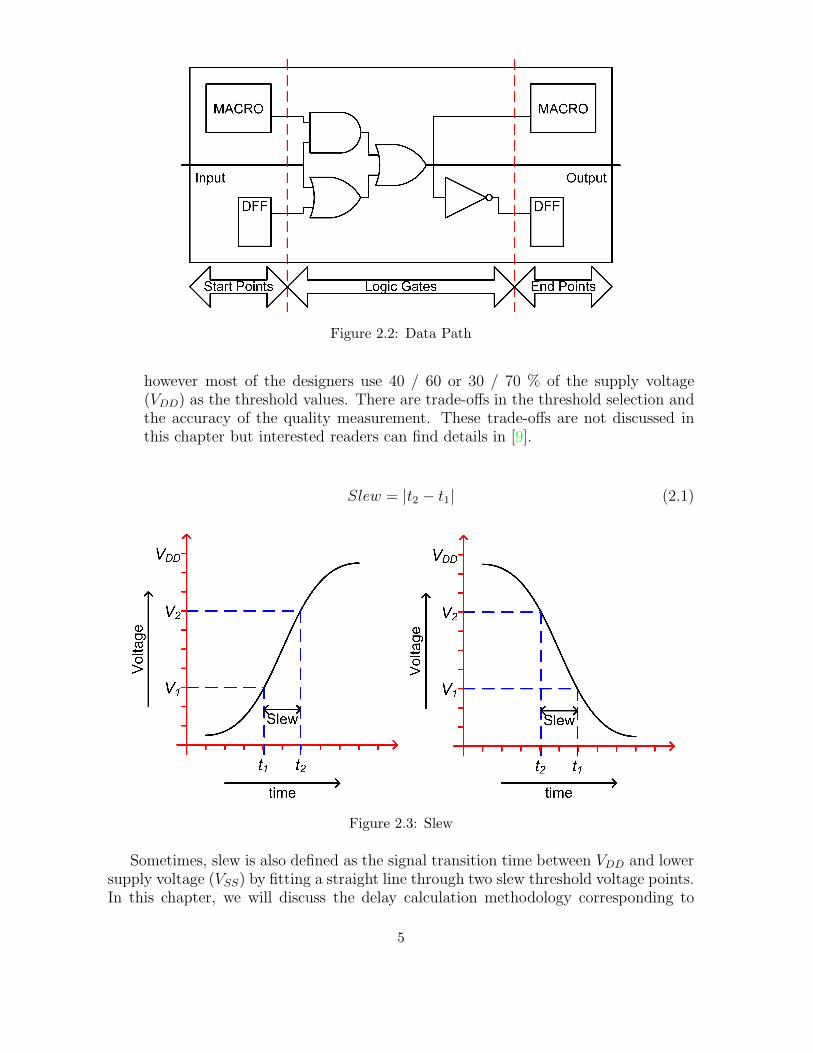
Figure 2.2: Data Path
however most of the designers use 40 / 60 or 30 / 70 % of the supply voltage(VDD) as the threshold values. There are trade-offs in the threshold selection andthe accuracy of the quality measurement. These trade-offs are not discussed inthis chapter but interested readers can find details in [9].
Slew = |t2 − t1| (2.1)
Figure 2.3: Slew
Sometimes, slew is also defined as the signal transition time between VDD and lowersupply voltage (VSS) by fitting a straight line through two slew threshold voltage points.In this chapter, we will discuss the delay calculation methodology corresponding to
5

the first definition only. Appropriate changes can be made to incorporate the seconddefinition into the delay calculation methodology.
Delay: Delay is defined as the time taken by a signal to travel from the input pinto the output pin of a circuit component. This circuit component could be aninterconnect, a gate, or a collection of gates and interconnects. The mathematicalequation for delay calculation is shown in (2.2). Here tdelay is the delay of thecomponent, and tin and tout are the times when the input and output signals crossthe delay threshold point which is usually VDD/2. However, the delay thresholdpoint can be changed if required. An example of the delay of an inverter alongwith the input and output waveforms is shown in Figure 2.4.
tdelay = tout − tin (2.2)
Figure 2.4: Illustration of a circuit component delay
A data signal traverses through the logic gates of a path and is captured by a DFFat the clock edge. Due to the internal delay of the DFF, some timing constraints areimposed on the input signals such as setup time, hold time, minimum clock width etc.Here we will concentrate on two major constraints: setup time and hold time, whichare defined below as:
Setup Time: To store the data correctly into the DFF, the input signal needs to bestable before the clock edge. The minimum time before the clock edge for whichthe input signal needs to be stable is known as the setup time.
Hold Time: Similar to the setup time constraint, the input signal needs to be stablefor some time after the clock edge to ensure correct functionality of the DFF. Theminimum time after the clock edge for which the input signal needs to be stableis known as the hold time.
6

A master-slave positive edge triggered flip-flop design using multiplexers (MUXes)is shown in Figure 2.5. A design of the same DFF with a pass transistor logic imple-mentation of the MUXes is shown in Figure 2.6. Here I1, I2, I3 . . . are the inverters andT1, T2, T3 . . . are the pass transistor logic. In these implementations, the internal nodeQm captures the input signal during the low level of the clock via I1, T1, and I3. Qm
retains the signal value during the high level of the clock with the help of the feedbackloop with I2, T2, and I3. Similarly, during the high level of the clock, the stored signalat Qm is passed to the output pin Q via I4, T3, and I6 and retains the output signal atthe low level of the clock with the help of the loop with I5, T4, and I6.
Figure 2.5: Master-Slave DFF with MUX
Figure 2.6: Master-Slave DFF with MUX as Pass Transistor Logic
To ensure that the correct signal value is stored into the DFF, the signal at the nodeQm and the loop I2, T2, and I3 should be stable before the rising edge of the clock.This constraint on the input signal gives the setup time of the DFF and is given in
tsetup = tdI1 + tdT1 + tdI3 + tdI2 (2.3)
where tdk denotes the delay due to component k. Since the signal propagation from thenode Qm to the output of the inverter I2 is considered in the setup time, the outputof the inverter I4 will also be stable at the rising edge of the clock. We should alsoconsider that the input signal should not change before it reaches from the internalnode Qm to the output pin Q, which gives the hold time of the DFF expressed as
thold = tdT3 + tdI6 (2.4)
7

Since a DFF stores new signal values only at the clock transition, the delay of aDFF is defined from the clock pin to the output pin and known as clock to Q delay(tck−q). Setup time (tsetup), hold time (thold), and clock to Q delay (tck−q) are depictedwith the help of the voltage waveforms in Figure 2.7.
Figure 2.7: Setup, Hold, and Clock to Q Delay in Waveform
For a DFF to DFF data path, as depicted in Figure 2.8, DFF1 is called the startpoint of the data path and DFF2 is called the end point of the data path. In this path,the signal at the start point changes at the clock edge and the signal at the end pointis captured at the next clock edge, which gives the relation between the maximumpermissible delay of the data path and the minimum possible clock period as given in
tperiod ≥ tpath delay + tsetup + thold
⇒ tperiod,min = tpath delay + tsetup + thold (2.5)
Here tpath delay is the delay of the logic gates and the interconnects between the startpoint and the end point of the data path, and tperiod,min is the minimum permissibletime period of the clock. The data path which has the longest path delay in the entirecircuit is also known as the critical path and it directly relates to the highest possiblefrequency of the circuit.
The path delay is comprised of the delay contribution due to each gate and theinterconnects of the data path. An example of a data path is depicted in Figure 2.9.Path delay equations for the data path from DFF1 to DFF3 (td1−3
) and DFF2 to DFF3
8

Figure 2.8: DFF to DFF Path
(td2−3) are given in (2.6) and (2.7) respectively.
td1−3= tDFF1
+ tn1+ tg1 + tn2
+ tg2 + tn3(2.6)
td2−3= MAX((tDFF2
+ tn6+ tn4
+ tg1 + tn2+ tg2 + tn3
),
(tDFF2+ tn6
+ tn5+ tg3 + tn7
+ tg2 + tn3)) (2.7)
Here tDFFkdenotes the delay contribution due to DFFk, tgk denotes the delay con-
tribution due to gate gk, and tnkdenotes the delay contribution due to interconnect nk.
Path delay calculation is a stage-by-stage approach in which the input of one gate tothe input of a successor gate is one stage. For example, DFF1 to g1, g1 to g2, and g2 toDFF3 are 3 stages of the data path from DFF1 to DFF3.
Figure 2.9: Path Delay
2.2 Static Timing Analysis
Up until this point we have understood that the critical path defines the maximumoperating frequency of the circuit. However in the industry, the required operatingfrequency of the circuit is pre defined and the circuit needs to be designed to achievethe target operating frequency. In this case, a designer needs to estimate the delayof each possible data path and make sure that the critical path is within the targetfrequency. This delay analysis is known as “Timing Analysis”. Considering the size of
9

an ASIC design (in the order of millions of gates), transistor level simulation (such asSimulation Program with Integrated Circuit Emphasis - SPICE ) analysis is not practicalfor the entire chip due to its high run time. This problem is addressed by modellingthe gate behaviour mathematically and performing mathematical analysis instead ofcircuit simulation. This analysis is known as “Static Timing Analysis (STA)”. The gatebehaviour of every standard cell is modelled and stored in a file, known as “StandardCell Library File” and used as an input in the ASIC design flow stages such as synthesis,placement, routing, and timing analysis.
The models of the gates stored in the standard cell library file are used to estimatethe delay of each gate of the data path. The delay of a gate depends on the input signalslew and the output load of the gate. This is discussed below in detail with the help ofan inverter.
A MOSFET implementation of an inverter is shown in Figure 2.10. When the inputsignal (In) is at logic ‘0’ i.e. VSS, the n-type MOSFET (NMOS) is in the cut-off modeand the p-type MOSFET (PMOS) is in the saturation mode which results in a pathfrom VDD to the output load via the PMOS and the output signal (Out) is at logic ‘1’i.e. VDD. When the input signal changes from logic ‘0’ to logic ‘1’ (i.e. rise transition),the PMOS is turned off which disconnects the path from VDD to the output pin. TheNMOS is turned on which opens a path from the output pin to VSS.
Figure 2.10: CMOS Inverter
The switching time of the output signal from VDD to VSS depends on two factors.Firstly, how quickly the NMOS is turned on and the PMOS is turned off and secondly,the time constant of the discharge circuit. The state of the NMOS and the PMOS ofan inverter depends on its gate voltage. The cut-off condition of both the NMOS andthe PMOS is given in (2.8) and (2.9), respectively.
Vin < VTN (2.8)
Vin > VDD − |VTP | (2.9)
The same is shown on the rising edge input signal waveform in Figure 2.11. HereVTN and VTP are the threshold voltages of the NMOS and the PMOS respectively, tnand tp are the time when the NMOS and the PMOS switches between the stages (ON/ OFF) respectively. The switching time of the output signal of the inverter dependson tn and tp which further depends on the input signal slew (|t2 − t1|).
10

Figure 2.11: ON and OFF state of the PMOS and the NMOS in an Inverter
Output signal transition time also depends on the RC time constant (τ) of thedischarge circuit. The charge accumulated on the output load (Cload) of the inverter isdischarged through the on resistance of the NMOS (Ron). The RC time constant (τ)is defined as
τ = Ron × Cload (2.10)
In this example, we understood that the delay of an inverter, for the input risetransition, depends on the input signal transition time (Slew) and the output load(Cload) of the inverter. A similar argument can be made for a fall transition of theinput signal.
The total effective load at the output pin of a gate is due to the on resistance of thedriver cell, interconnect impedance, and input impedance of the receiver cell [10, 11, 12].We can see in Figure 2.10 that the effective output impedance of an inverter will havea contribution of the resistance from the output node to the VDD and the VSS viathe PMOS and the NMOS respectively. This output resistance of the inverter is veryhigh as compare to the interconnect resistance in higher technology nodes. Thus,the resistive component of the interconnect can be ignored, and this will introduce anegligible error in delay calculation. Also note that, due to the very small dimension ofthe interconnect, the inductance of the interconnect is small. In a low frequency circuit,the equivalent impedance due to this inductance is very small in comparison with theequivalent impedance due to the resistance and capacitance of the interconnect and canbe ignored. These assumptions result in a simplified model of the total effective load atthe output pin of a gate as an effective capacitance only for higher technology nodes.However, in the lower technology nodes, the interconnect resistance can no longer beignored [13].
Now, we can say that the output voltage waveform of a driver can be defined fora given set of the input signal slew and output load, and the delay for STA can beestimated.
11

Various methodologies have been proposed to model the gate behavior for the delayestimation in STA. Traditionally, the Non-Linear Delay Model (NLDM) has been usedfor the delay estimation [14]. However due to increase in frequency and device shrinking,the relative error introduced by NLDM is no longer acceptable. Various improvedmodelling schemes have been proposed. The Composite Current Source (CCS) [15, 16,17, 18] and the Effective Current Source Model (ECSM) [9, 19] are well known industrystandard modelling schemes. We will briefly discuss NLDM, CCS and ECSM modellingschemes in the following subsections.
2.2.1 Non-linear Delay Model
NLDM is the traditionally used modelling scheme, in which the gate delay is modelledusing lookup tables. If we neglect the resistive component of the impedance from theeffective load of a cell (as discussed in Section 2.2), then the cell delay is dependent ontwo parameters: input signal slew and output effective capacitive load (for a specifiedProcess, Voltage, and Temperature (PVT)). We also know that the MOSFET behaviourdepends on the input signal transition i.e. rise transition and fall transition. In NLDM,cell delay is modelled in a two dimensional lookup table for each transition as shownin Table 2.1. Here Sin is the input signal slew, Cout is the effective output capacitiveload of a cell and tdelay is the gate delay.
Table 2.1: NLDM based cell delay (tdelay) lookup table
Input Signal Effective Output CapacitanceSlew Cout1 Cout2 Cout3
Sin1tdelay tdelay tdelay
Sin2tdelay tdelay tdelay
Sin3tdelay tdelay tdelay
These gate delays are obtained from multiple SPICE simulations for every set of Sin
and Cout. Since the lookup table contains only a small set of Sin and Cout, interpolationor extrapolation are required to evaluate tdelay and Sout for the desired set of Sin andCout.
Being a very simple lookup table, NLDM makes delay calculation very fast at thecost of accuracy. Primary cause of the accuracy loss is due to interpolation, processvariation, on-chip variation, and the complex behavior the MOSFET at the smallertechnology nodes [15, 20]. Several more advanced modelling schemes have been de-veloped in which the complex behaviour of the cell and the signal waveforms can becaptured more accurately. These advanced modelling schemes reduce the relative errorin the delay calculation. The Composite Current Source (CCS) Model from Synopsysand the Effective Current Source Model (ECSM) from Cadence are the most well knownindustry standard modelling schemes of this type.
2.2.2 Composite Current Source Model
Similar to NLDM, characterization in a CCS model is also carried out with a small setof combinations of input signal slew and output effective capacitive load. However, in
12

contrast with NLDM, CCS contains the output current waveform (see Figure 2.12) inthe lookup table as shown in Table 2.2. Here Iout(t) is the output current waveform.It is represented by a set of paired current and time values. In the library file, twovectors are used to store simulation time and corresponding output current value forevery pair of Sin and Cout.
Figure 2.12: Measurement of Iout(t) for a set of Sin and Cout
Table 2.2: CCS based output current waveform (Iout(t)) lookup table
Input Signal Effective Output CapacitanceSlew Cout1 Cout2 Cout3
Sin1Iout(t) Iout(t) Iout(t)
Sin2Iout(t) Iout(t) Iout(t)
Sin3Iout(t) Iout(t) Iout(t)
In contrast with NLDM, CCS does not define gate delay value for a given set ofinput signal slew and an effective output capacitive load. Instead of this, CCS has theoutput current waveform which needs to be processed to extract the delay value. Theinaccuracy introduced by the current waveform interpolation in CCS is smaller thanthe inaccuracy introduced by the delay and slew interpolation in NLDM [15, 21].
2.2.3 Effective Current Source Model
ECSM is another well known industry standard modelling scheme for standard celldelay. In contrast with CCS, it contains the output voltage waveform of the cell (Vout(t))(see Figure 2.13) in a lookup table instead of the current waveform as shown in Table 2.3.Similar to CCS, the voltage waveform in ECSM is represented by a set of paired voltageand time values. They are stored in the library file using two vectors, one for thesimulation time and other one for corresponding output voltage magnitude.
Table 2.3: ECSM based output voltage waveform (Vout(t)) lookup table
Input Signal Effective Output CapacitanceSlew Cout1 Cout2 Cout3
Sin1Vout(t) Vout(t) Vout(t)
Sin2Vout(t) Vout(t) Vout(t)
Sin3Vout(t) Vout(t) Vout(t)
13

Figure 2.13: Measurement of Vout(t) for a set of Sin and Cout
Similar to the delay calculation in CCS, the output voltage waveform of ECSMneeds to be processed to extract the delay value. The inaccuracy introduced by thevoltage waveform interpolation in ECSM is smaller than the inaccuracy introduced bythe delay and the slew interpolation in NLDM [9, 21].
2.3 Statistical Static Timing Analysis
As discussed in Section 2.2, the delay of a gate depends on the input signal slew andoutput load of the cell. Along with this, the delay of a gate also depends on the currentthrough the PMOS / NMOS transistors while charging or discharging the load. Thecurrent of the MOSFET further depends on its channel length (L), channel width (W ),oxide thickness (tox), doping concentration, supply voltage, temperature, etc. Since theMOSFET is also called a device, the channel length, channel width, oxide thicknessand doping concentration are also known as device parameters. There are many moredevice parameters which are not mentioned here. The value of these device parametersdepends on the fabrication process of the integrated circuit. Therefore, the deviceparameters are also known as process parameters. It can be said that the delay of agate depends on the Process, Voltage, and Temperature (PVT).
The processing steps during integrated circuit fabrication are mainly mechanical,thermal, chemical and optical. Due to the uncertainty in these steps, the measuredvalues of the process parameters might deviate from the expected values. This phe-nomenon is known as process variation. The resistive component of interconnect intro-duces voltage drop in the wire which results in variations in the supply voltage. Heatdissipation is also not uniform on the entire chip due to different switching activitiesin different regions of the chip. This causes temperature variations on the chip. Allthese effects result in variation of the PVT values which results in variation in the delayof a gate. Delay variations result in the variation of the maximum possible operatingfrequency of the circuit. It might also result in setup and hold violations and affect thecorrectness of the circuit functionality.
Delay estimation in the STA methodology does not consider the variations in thePVT parameters. Instead of this, STA is performed multiple times to estimate thedelay in various PVT corners such as best case and worst case corners. In the bestcase corner, smallest delay is considered which implies fast process (low capacitance,fast transistors), high voltage and low temperature. Similarly, in the worst case corner,
14

highest delay is considered which implies slow process (high capacitance, slow transis-tors), low voltage and high temperature. This methodology is well known as cornercase analysis. Additionally, the k-factor modelling approach is also used. K-factormodelling is a method to scale the delay of every cell in the library by a fixed factor k.The scaling factor k mostly varies between 0.9 and 1.1. This scaling is to protect thedesign from unknown PVT variations. This k-factor modelling introduces deviationfrom the SPICE simulation.
As we are moving towards nanometer technology, process variation is increasing,causing significant uncertainty in the delay estimation [3] which greatly impacts theyield [4, 5]. As a consequence, the accuracy of the conventional Static Timing Anal-ysis (STA) with corner to estimate digital circuit performance in advance technologyprocesses is a serious concern [22]. Due to these PVT variations, the delay really isa statistical parameter instead of a deterministic one. The methodology of estimatingthe timing of a data path with PVT variation is known as Statistical Static TimingAnalysis (SSTA) [23, 24, 25, 26].
2.4 Circuit Simulation and Analysis Environment
The primary requirement for the implementation of the STA and SSTA methodologiesis circuit simulation. Circuit simulation is a process of mathematically estimating theexpected behavior of the physical circuit. Being a mathematical analysis tool, it needsa mathematical model of each circuit component to perform the circuit simulation. Atearlier nodes of the IC technology development, simple MOSFET models have beenused. However, due to device shrinking, various physical effects (like short channeleffect, gate leakage etc.) are nowadays playing a significant role in the device behav-ior. Many detailed models have been developed to represent the complex behavior ofthe MOSFET. EKV (developed by C. C. Enz, F. Krummenacher and E. A. Vittoz,hence the initials EKV) [27] from EPFL (Ecole Polytechnique Federale de Lausanne)and BSIM (Berkeley Short-channel IGFET Model) [28] from UCB (University of Cal-ifornia, Berkeley) are well known industry standard models. A variant of the BSIMmodel, known as BSIM4 [29] is predominantly used in state of the art integrated cir-cuit development. The parameters of these models are extracted by characterizationof the MOSFET developed by fabrication plant (fab). These parameters are fab andtechnology dependent.
As technology is shrinking, various behaviors (like process variations) are signifi-cantly affecting the performance of the device. Research activities are necessary tounderstand the behavior of the future transistors in advance technology nodes. TheITRS (International Technology Roadmap for Semiconductor) [30] is actively involvedin defining the future technology nodes. MOSFET models are also required for fu-ture technology nodes for use in research activities. The PTM (Predictive TechnologyModel) [31] is a well known set of technology models for future transistors as specifiedby ITRS. PTM provides SPICE based predictive BSIM4 models which can be used withsimulation tools to analyse circuit behavior. Therefore, with PTM, research work canstart well before the real development of the advance semiconductor technologies hascompleted. The Nangate Open Cell Library [32] is another well know name among the
15

researchers for the circuit design kit based on the PTM technology. It offers predictivestandard cell libraries designed with PTM technologies.
For the 45nm technology node, two types of PTM models are available, namely PTMHP for high performance design and PTM LP for low power design. The 45nm BSIM4model of the MOSFET based on the PTM HP technology is used in the work relatedto this thesis. Additionally, standard cell circuit design based on the Nangete opencell library is used for analyzing the delay variations due to PVT variations. CadenceSpectre [33] is used for circuit simulation and MATLAB [34] for data processing. Sincethe input technology file for Spectre are not quite the same as for SPICE, appropriatemodifications have been made in the PTM model such that it can be used with CadenceSpectre.
The activities of this thesis work are under the umbrella of the MODERNProject [35]. One of the objectives of the MODERN project is to develop a SSTAengine and methodology flow to address the problems, which arise due to PVT varia-tions. The MODERN project is targeting to address these problems at the root level.We know that the root of the inaccuracy in the delay estimation is due to the lookupbased model with corner case analysis and k-factor approach. The highest accuracycan be achieved by using full SPICE-level simulation of each standard cell for the delayestimation. However, due to the high run time of the SPICE simulation, this is nota practical approach for digital circuits. Therefore, a fast circuit simulator is beingdeveloped in the MODERN project. The SSTA engine of the MODERN project willhave this fast circuit simulator and delay of each gate will be estimated on the fly. Thiscircuit simulation will increase the accuracy of the delay estimation due to the PVTvariations. Furthermore, the accuracy of the delay variation estimation is increased bypreserving various possible waveforms due to PVT variations at every input and outputpins of the standard cells. These waveform collections are called “sets of waveforms”.Sets of waveforms as a representation of uncertainty in a waveform, and the possibleapproaches to preserve the waveforms are discussed in Chapter 5.
2.5 Summary
The basics of digital circuit design and its terminologies like Data Path, Delay, Slew,Setup Time, and Hold Time are introduced in this chapter. Following this, the stateof the art methodologies for STA are presented. NLDM, CCS and ESCM are theindustry practice standard cell models for STA. However, due to the variations inPVT, the standard cell behavior is not deterministic anymore. Therefore, there is aneed of SSTA which is also discussed in this chapter. The MOSFET model, technologyfiles, simulation and analysis environment are also introduced.
16

Delay Variations 3As discussed in Chapter 2 that the maximum operating frequency depends on the delayof standard cells, there is a need to analyze the variation in the delay of standard cellsdue to PVT variations. There are two major objectives of this work. Firstly, understandthe variation in the standard cell delay due to the variations in PVT parameters.Secondly, develop an environment to measure the variation of the delay, slew, andother circuit parameters of the standard cells due to the PVT parameters. Here fivePVT parameters are considered to be varying; they are channel length (L), channelwidth (W ), threshold voltage (Vth), supply voltage (VDD), and temperature (T ).
The organization of the chapter is as follows: the variations in the PVT parametersfor the 45nm technology node are estimated in Section 3.1, followed by the circuitsimulation configuration in Section 3.2. The variations in the delay of an inverter dueto the variations in PVT parameters are discussed in Section 3.3. In this section, thedelay variation analysis is subdivided into three categories, namely, variations in thedelay due to each PVT parameter separately, combinations of two parameters, and arealistic scenario with all the parameters varying together. The delay variations donot follow a Gaussian distribution, therefore there is a need for higher order statisticalmoments as discussed in Section 3.4. The variations in the delay of various standardcells are discussed in Section 3.5. At the end, a summary of the chapter is presentedin Section 3.6.
3.1 Variations in the PVT parameters
Since we are working on predictive technology models, fabrication data is not availableto estimate the spread in the process variation. At this development stage, we havemade an educated guess by extrapolating the spread of the process variations data fromthe existing technology nodes. Variation spread of the channel length (L), channelwidth (W ), and threshold voltage (Vth) for technology nodes up to 70nm are reportedin Table 3.1 [3]. The extrapolated spread data of the process parameters for the 45nmtechnology node is included in the last row of the same table. Here σX is the standarddeviation of parameter X and 3σX is a measure of the spread of the parameter X .
The nominal value (µ) and spread (3σ) of the two physical parameters, L & W , areplotted in Figure 3.1a and Figure 3.1b respectively. Here nominal values of differenttechnology nodes are on the X-axis and their spreads are on the Y-axis. These figuresshow a very strong linear relationship. Therefore, a linear best fit curve is used toextrapolate the spread of L and W to the 45nm technology node. A linear best fitcurve and extrapolation point for the 45nm node are also shown in the same figures.
The threshold voltage (Vth) depends on various physical parameters, e.g. gate oxidethickness (tox), doping concentration (N) etc. Since the spread of these physical param-
17

Table 3.1: Technology process parameter trends based on [3]
L (nm) 3σL (nm) W (nm) 3σW (nm) Vth (mV) 3σVth(mV)
250 80 800 200 500 50
180 60 650 170 450 45
120 45 500 140 400 40
100 40 400 120 350 40
70 33 300 100 300 40
45 26 90 58 469 37
eters are not available for the existing technologies, the trend of the spread of the Vth
is analysed against the technology node itself. Nominal values of the technology node(µL) and the spread of the threshold voltage (σVth
) are plotted in Figure 3.1c. Thereare two important observations with the threshold voltage variation. First, Vth in the45nm PTM is relatively high, and second, the absolute value of the Vth spread (3σVth
)is constant in 120nm technology nodes and below. These observations are discussedhere.
As technology is shrinking, the channel length and channel width are reducing.However, the gate oxide has reached to a very low thickness, and further reduction inthe oxide thickness is not possible. High-k dielectric materials are being used insteadof lowering the gate oxide thickness. Here k is the relative dielectric constant of thematerial filled between gate and channel. The relations between Vth, tox, and k aregiven below:
Vth ∝toxk
(3.1)
Based on this theory, the threshold voltage should reduce while reducing each tech-nology nodes. The reduction can be seen from 250nm to 70nm technology nodes (seeTable 3.1). Following a similar trend, Vth in 45nm should reduce. However, in the 45nmPTM model, the threshold voltage is increased in comparison with previous technologynodes. There is not enough information available about the PTM model to understandthis behaviour.
The variation in the threshold voltage also depends on the variation in dopingconcentration (N). As device dimensions are shrinking, the absolute number of dopantatoms in a device is reducing. In technology nodes above 90nm, the numbers of dopantatoms are still high and a variation in this number should have just a small impact onthe threshold voltage. Therefore, the effect of variation in tox is the dominating factorfor Vth variation and its spread should decrease with technology shrinking. However,in sub 90nm technology nodes, the numbers of dopant atom are already within severaltens and the variation in the number of dopant atoms should significantly influence thethreshold voltage variation. It implies that in sub 90nm technology nodes, the spread inVth should increase. Based on the existing technology data, the spread of Vth is reducingfor higher technology nodes and then it become constant for 120nm technology nodeand below.
As the dominating physical variation for the variation in Vth is different in higher and
18

lower technology nodes, any extrapolation on this data might lead to significant errorin the spread estimation of the gate delay. Experiments (see Section 3.3) show that thecontribution of the threshold voltage variation in the delay variation of INV X1 is only10% whereas the contribution of L and W are 53% and 63% respectively. Because ofthe very small impact of the threshold voltage variation in the delay variation, a linearbest fit curve is used to extrapolate the spread of the Vth in 45nm technology node.The linear best fit curve and extrapolated spread of Vth in the 45nm technology nodeare plotted in Figure 3.1c.
50 100 150 200 250
30
40
50
60
70
80
µLeff
(nm)
3σLe
ff (nm
)
3σLeff
(nm) vs µLeff
(nm)
expfitest
(a) Spread estimation for L
200 400 600 80050
100
150
200
µW
(nm)
3σW
(nm
)
3σW
(nm) vs µW
(nm)
expfitest
(b) Spread estimation for W
50 100 150 200 25036
38
40
42
44
46
48
50
µLeff
(nm)
3σV
th (
mV
)
3σVth
(mV) vs µLeff
(nm)
expfitest
(c) Spread estimation for Vth
Figure 3.1: Spread estimation for PTM Model
Apart from L, W , and Vth, we need the spread for the supply voltage (VDD) andthe temperature (T ) as well. We have considered a temperature variation from 15◦C to75◦C, which can be represented as a nominal value of 45◦C and 3σT of 30◦C. Since thetemperature variation is application dependent, the designer can change the variationduring the analysis. For the supply voltage, we can assume that the spread is 15% ofits nominal value. In this experimental setup, we have considered a supply voltage of1.00V and 3σVDD
equal to 0.15V. The nominal values (µ), their spread (3σ), and the
19

spread variation in percentage with respect to its nominal value (3σ%) for all the fivePVT parameters are summarised in Table 3.2.
Table 3.2: Spread of the PVT parameters
Parameter Nominal (µ) Spread (3σ) 3σ%
L 45nm 26nm 58%
W 90nm 58nm 64%
Vth 469mV 37mV 8%
T 45◦C 30◦C 67%
VDD 1.0V 0.15V 15%
It is important to note that the spread of the channel length L and channel widthW are IC fabrication process dependent. Therefore, it can be safely assumed that thespread is independent of the absolute value of the L and W . This implies that the 3σvalues of L and W remain constant for various sizes of the standard cells and theirvalues can be taken from the Table 3.2.
The process parameters are either physical parameters (e.g. L, W ) or they dependon physical parameters (e.g. Vth depends on gate oxide thickness, doping concentrationetc.). These physical parameters further depend on fabrication processing steps andtheir parameters. In general, fabrication process parameters have a non-linear relation-ship with the physical parameters [22]. It can be assume that the fabrication processingparameters may follow a Gaussian distribution due to central limit theorem [36]. How-ever, due to the non-linear relationship between fabrication parameters and physicalparameters, the physical parameters might not follow a Gaussian distribution. There-fore, in general, the process parameters do not follow a Gaussian distribution. However,it is very complicated to measure the exact distribution of each process parameters. Inindustrial practice, all parameters are usually assumed to follow a Gaussian distribu-tion. Following this industrial practice, for the rest of this chapter, each parameter isconsidered to follow a Gaussian distribution.
3.2 Circuit Simulation Configuration
Based on the 45nm Nangate open cell library, the nominal size of the channel length(Ln) and channel width (Wn) of an NMOS in the smallest inverter (INV X1) shouldbe 50nm and 90nm respectively. Similarly, the nominal size of the channel length(Lp) and channel width (Wp) of a PMOS in the same inverter should be 50nm and135nm respectively. The 3σ spread of the L and W for both NMOS and PMOS can betaken from Table 3.2, and the values are 26nm and 58nm respectively. For a Gaussiandistribution of any random variable, a spread of ±3σ around its mean (µ) covers 99.8%probability of the random variable. Due to this, in industrial practice, (µ±3σ) coverageis used for all the process parameters in the SSTA methodology. Therefore, in thisanalysis, the circuit simulation is carried out in the range of (µL ± 3σL) for channellength L and (µW ±3σW ) for channel width W . The nominal values, 3σ spread and therequired range of L and W of the NMOS and PMOS in INV X1 are given in Table 3.3.
20

Table 3.3: Nominal and 3σ range for Nangate INV X1 inverter
Name Nominal (µ) Spread (3σ) Range (µ± 3σ)
Ln 50nm 26nm 24nm to 76nm
Wn 90nm 58nm 32nm to 148nm
Lp 50nm 26nm 24nm to 76nm
Wp 135nm 58nm 77nm to 193nm
During simulation of the INV X1 using the Spectre circuit simulator and the BSIM4model from PTM, we encountered the following two problems. First, Spectre exits witha fatal error while simulating the inverter with a channel length smaller than 32nmwhile keeping the rest of the parameters at their nominal values. This fatal error isdue to the fact that the effective channel length of the given MOSFET in the PTMtechnology is becoming negative. Since the required range for L has a lowest value of24nm, the inverter can not be simulated for the entire required range. Second, Spectrecan simulate the inverter with the specified range of the channel width, but it has beenobserved in the simulation experiments that the delay of the inverter does not changefor a channel width smaller that 45nm while keeping the rest of the parameters at theirnominal values. This might be because the MOSFET model in 45nm PTM technologyis not well defined and tested below 45nm of channel width. The variation in the delayof an INV X1 due to channel width variation is shown in Figure 3.2.
40 60 80 100 120 140
60
80
100
120
140
160
180
W (nm)
dela
y (p
s)
delay vs W
Figure 3.2: Delay of INV X1 vs W for µW = 90nm and 3σW = 58nm
These problems demonstrate that the available 45nm PTM model is not very welldefined for very small MOSFETs. In this chapter, these problems are addressed byincreasing the nominal values of L and W such that the (µ ± 3σ) ranges of these
21

parameters can be simulated meaningfully in Spectre. Therefore, the minimum sizeof L is taken as 60nm and the minimum size of W is taken as 105nm. The nominalvalues, 3σ spread and the required range of L and W for the proposed MOSFET sizeare given in Table 3.4. The minimum sizes of L and W reported in this table are usedin various other standard cells as well.
Table 3.4: Nominal and 3σ range for modified INV X1 inverter
Name Nominal (µ) Spread (3σ) Range (µ± 3σ)
Ln 60nm 26nm 34nm to 86nm
Wn 105nm 58nm 47nm to 163nm
Lp 60nm 26nm 34nm to 86nm
Wp 157.5nm 58nm 99.5nm to 215.5nm
The delay variation analysis is carried out for various standard cells. Based onthe number of parameter variations, the analysis is classified into three categories, viz.delay variation due to individual parameter, due to a combination of two parameters,and due to variations of all PVT parameters together. Delay variation in an INV X1inverter is discussed in detail first, followed by the delay variation of other standardcells.
To make a consistent circuit environment among all the gates, the input signal slewand output capacitive load of each standard cell is kept the same. Here, slew thresholdvoltages are 10% and 90% of VDD. Based on the Nangate open cell library of 45nm, anapproximated average of the signal slew is 8ps and effective load is 10fF. These signalslew and capacitive load values are used in every standard cell simulation for the delayvariation analysis.
3.3 Delay variation in an inverter
The circuit configuration for the INV X1 inverter is given in Figure 3.3. Due to thevery close physical location of Ln and Lp, they are assumed to be highly correlated.Similarly, Wn and Wp are also assumed to be highly correlated. Threshold voltagevariation in PMOS and NMOS are also assumed to be highly correlated because oftwo main reasons. First, at any transition, signal value can change either from lowto high value or high to low value. Therefore, either PMOS or NMOS will be activeto charge or discharge the effective capacitive load. Since most of the times duringtransition either NMOS or PMOS is active, keeping high correlation in their thresholdvoltage does not introduce a significant error. Second, keeping high correlation in thethreshold voltages reduces the total number of independent parameters in the circuitsimulation. This in turn reduces the complexity and number of simulation iterationsrequired during circuit simulation.
The relation between channel length, channel width, and threshold voltages of bothNMOS and PMOS are given below. The relation between Wn and Wp are taken fromthe Nangate library. The nominal threshold voltage of NMOS (Vthn
) is positive whereasthe nominal threshold voltage of PMOS (Vthp
) is negative. Additionally, Vthnincreases
22

SinCload
VDD
Lp
Wp
Vthp
Ln
Wn
Vthn
PMOS
NMOS
Figure 3.3: INV X1 simulation configuration
with increase in doping concentration whereas Vthpdecreases with the doping concentra-
tion. Therefore, a negative correlation among them is considered here. All the circuitparameters used in the simulation of the INV X1 and their ranges are summarised inTable 3.5.
Ln = L+∆L (3.2)
Wn = W +∆W (3.3)
Lp = L+∆L (3.4)
Wp = 1.5 ·W +∆W (3.5)
∆Vthn= ∆Vth (3.6)
∆Vthp= −∆Vth (3.7)
Table 3.5: INV X1 simulation configuration
Name Value Range
L 60nm ± 26nm
W 105nm ± 58nm
VDD 1V ± 0.15V
∆Vth 0 ± 37mV
T 45◦C ± 30◦C
Sin 8ps N.A.
Cload 10fF N.A.
The delay variation of this inverter due to individual parameters, combinations oftwo parameters, and due to all the parameters together is discussed in the followingsubsections.
23

3.3.1 Individual Parameter Variation
In this setup, it has been assumed that only one parameter is varying and rest of theparameters are at their respective nominal values. The purpose of this experiment isto understand the impact in the delay variation due to the individual PVT parametersseparately. A plot of the delay of an inverter INV X1 as a function of the channel length(L) is shown in Figure 3.4a. Here, channel length is on the X-axis and delay is on theY-axis. This figure shows that the delay is not a linear function of L in the interestedrange of variation. Due to this non-linear relation, the delay variation will not follow aGaussian distribution, even if the channel length follows a Gaussian distribution.
The probability density function (pdf) of delay variation and its Gaussian approxi-mation are shown in Figure 3.4b. Here delay is on the X-axis and probability is on theY-axis. The circle markers are the pdf of the delay from the simulation experiment andthe solid line is the approximated Gaussian distribution. The mean (µ) and standarddeviation (σ) of the delay are also reported in the same figure. The approximatedGaussian distribution is generated while keeping the same value of µ and σ of the delaydistribution.
The plot of the pdf of the delay shows that the delay variation does not follow aGaussian distribution exactly. Similarly, the pdf of the delay due to the variations inW and VDD also does not follow a Gaussian distribution. However, the pdf of the delaydue to the variations in Vth and T are very close to a Gaussian distribution. Sincethere is nothing new to learn from these other plots, the delay function and pdf plotsdue to each parameter variation are added in Appendix A. The non-linear relation ofthe delay with respect to each parameter can be seen in these plots. Additionally, thepdf of the delay variation does not follow their approximated Gaussian distribution.The methodology to estimate µ, σ and the pdf of the simulation output (e.g. delayof an standard cell) is discussed in Chapter 4. The mean (µ), spread (3σ) and spreadpercentage with respect to its mean value (3σ%) of the delay due to each parametervariation are reported in Table 3.6.
Table 3.6: Delay spread of INV X1 due to individual parameter variation
Parameter Mean (µ) (ps) Spread (3σ) (ps) 3σ%
L 69.69 36.90 52.95
W 73.16 45.81 62.62
Vth 70.36 7.14 10.15
T 70.41 12.69 18.02
VDD 70.71 12.48 17.65
It is important to note that the mean of the delay (µ) due to the variation in channelwidth (W ) is relatively high when compared to the delay mean due to other parametervariations. The reason for this behaviour is as following. In the specified range of the 3σvariations in the PVT parameters, the delay variation is highly non-linear with respectto W as compared to other parameters. The variations of the delay as a function ofeach individual parameter are given in Appendix A. This highly non-linear relation isdue to the fact that the drain-source current (Ids) in a MOSFET is directly proportional
24

40 50 60 70 80
20
30
40
50
60
70
80
90
100
L (nm)
dela
y (p
s)
delay vs L
(a) Delay as a function of L
20 40 60 80 100
0
0.5
1
1.5
2
2.5
3
3.5x 10
10
delay (ps)
pdf of delay due to L
expnorm
µ = 69.6873 psσ = 12.3028 ps
(b) Delay distribution pdf due to L
Figure 3.4: Delay variation due to L
to W and the delay is inversely proportional to Ids. Therefore, the delay is inverselyproportional to W . Due to this inverse relation between delay and W , the mean of thedelay is shifted from the nominal delay value. It can also be observed that W is theprimary cause for delay not following a Gaussian distribution.
25

Based on this experiment, we can say that the channel length (L) and channel width(W ) are having the highest impact on the delay. This implies that the SSTA simulatorshould have higher accuracy for the modelling of L and W than that of VDD and Vth.This information is very useful for the development of the SSTA engine.
3.3.2 Combination of two parameters variations
After understanding the effect of the individual parameter variations on the delay of aninverter, pairs of two parameters variations have been used to understand their jointinfluence on the delay variation. Due to unavailability of the covariance information,it has been assume that the parameters are independent.
In this work, five PVT parameters (L, W , Vth, T , VDD) are considered to havevariation which results in ten paired combinations. All these possible pairs have beenused to analyze their effect on the delay variation. However, only the variation in thedelay due to W and L are discusses in detail. Since the delay variation due to otherparameter pairs also shows similar behaviour, they have not been discussed in detail.However, a summary of all other combinations of variables is discussed here. The plotsof the delay variation due to other pair of parameters can be found in Appendix A.
The delay as a function of L and W is shown in Figure 3.5a. Here W is on the X-axis, L is on the Y-axis and the delay is on the Z-axis. There are two main observationsin the plot. First, the delay values are clipped for high L and low W . This indicatesthat the 45nm PTM model is not well defined in this region. However, due to verylow probability of this segment, the inaccurate behaviour of the PTM model has beenignored. The second observation is about the linearity of the delay variation due tovariation in L and W . Since the plot is not a linear plane, the delay distribution shouldbe deviating from a Gaussian distribution, even if the input parameters (L and W ) arefollowing a Gaussian distribution.
The pdf of delay variation and its Gaussian approximation are shown in Figure 3.5b.Similar to the pdf plot of the delay due to one parameter variation, in this figure thedelay is on the X-axis and probability is on the Y-axis. The circle markers are thepdf of the delay from the simulation experiment and the solid line is the approximatedGaussian distribution. The mean (µ) and standard deviation (σ) of the delay arealso reported in the same figure. Again, the approximated Gaussian distribution isgenerated while keeping the same value of µ and σ of the delay distribution. The mean(µ), spread (3σ) and spread percentage with respect to its mean value of the delay dueto each pair of parameter combinations are reported in Table 3.7a, Table 3.7b, andTable 3.7c respectively.
There are two important observations in the result of this simulation experiment.First, in each pair where W is one of the parameters, the mean of the delay is higherthan the mean of the delay due to other pairs. This is due to the fact that delay isinversely proportional to W in the interested range of variation. A similar behaviourhas been observed in individual parameter variations. The second observation is inthe pdf curve of the delay. It can be seen that there are a few outlier points in thepdf curve; therefore the curve is not very smooth. This is because limited simulationiterations have been used in these experiments. The smoothness of the curve can beimproved by increasing the number of simulation iterations. However, it is important
26

40
60
8050
100150
50
100
150
W (nm)
delay vs W vs L
L (nm)
dela
y (p
s)
(a) Delay as a function of W & L
50 100 150
0
0.5
1
1.5
2
x 1010
delay (ps)
pdf of delay due to W and L
expnorm
µ = 72.5292 psσ = 20.0592 ps
(b) Delay distribution pdf due to W & L
Figure 3.5: Delay variation due to W & L
to note that the pdf curve is mainly used to visualize the distribution of the delay,and their statistical moments (µ and σ) are used in SSTA methodology. The proposedfast statistical moment estimation method has been used to estimate these statisticalmoments and this methodology is presented in Chapter 4. Furthermore, it has been
27

Mean (µ) (ps) L W Vth T
W 72.53
Vth 69.75 73.24
T 69.79 73.28 70.47
VDD 70.10 73.60 70.79 70.83
(a) Mean (µ) of delay variation due to two parameter variations
Spread (3σ) (ps) L W Vth T
W 60.18
Vth 37.77 46.62
T 39.48 48.00 14.61
VDD 39.45 48.12 14.55 17.91
(b) Spread (3σ) of delay variation due to two parameter variations
3σ% L W Vth T
W 82.97
Vth 54.15 63.65
T 56.57 65.50 20.73
VDD 56.28 65.38 20.55 25.29
(c) Spread % (3σ%) of delay variation due to two parameter variations
Table 3.7: Delay variation due to two parameter variations
shown that only a very small number of iterations is needed to estimate the statisticalmoments in the proposed methodology. Having more simulation iterations does notchange the value of the statistical moments of the delay variation. Therefore, thenon smoothness of the pdf curve dues not affect the accuracy of the estimation of thestatistical moments.
The results of one parameter variation and two parameter variations are consistent,i.e. the variation in the L and W are the primary contributors of the delay variation.The pdf plots show that the distribution of the delay with two parameters varying isalso not following a Gaussian distribution.
3.3.3 A realistic PVT variation
After analyzing the effect of the variation in individual parameters and pairs of twoparameters on the delay of an inverter, an experiment is carried out with all five pa-rameters variations together. This scenario is used to produce delay variations closelymatching reality in real silicon. Since the delay data in this experiment has six dimen-sions, the delay as a function of the PVT parameters can not be plotted.
The pdf of the delay variation and its Gaussian approximation is plotted in Fig-ure 3.6. Similar to the previous pdf plots, the delay is on the X-axis and probability ison the Y-axis. The circle markers are the pdf of the delay from the simulation experi-ment and the solid line is the approximated Gaussian distribution. The mean (µ) andstandard deviation (σ) of delay are also reported in the same figure. The approximatedGaussian distribution is using the same value of µ and σ of the delay distribution. The
28

mean (µ), spread (3σ) and spread percentage with respect to its mean value of thedelay are reported in Table 3.8.
50 100 150
0
0.5
1
1.5
2
x 1010
delay (ps)
pdf of delay
expnorm
µ = 73.1744 psσ = 21.7734 ps
Figure 3.6: Delay distribution pdf due to realistic PVT variations
Table 3.8: Delay variation due to realistic PVT variation
Value
Mean (µ) (ps) 73.17
Spread (3σ) (ps) 65.31
3σ% 89.26
The conclusion of this experiment is that the delay distribution in a realistic PVTvariation scenario does not follow a Gaussian distribution. Therefore, there is a needto quantitatively measure the deviation of the delay distribution from its correspond-ing Gaussian distribution. The quantitative measure of the distribution deviation isdiscussed in the next section.
3.4 Higher order statistical moments
The pdf of delay in a realistic scenario of PVT variations is significantly deviatedfrom its corresponding Gaussian distribution. This indicates that imposing a Gaussiandistribution on the delay variation during SSTA is introducing an error in the delayvariation estimation. The deviation of the pdf of delay from its corresponding Gaussiandistribution can be captured with higher order statistical moments. Therefore, it isimportant to include higher order statistical moments in SSTA for accurate analysis.
29
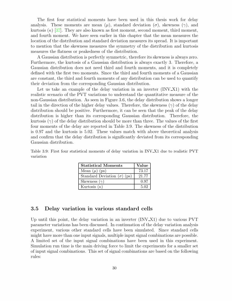
The first four statistical moments have been used in this thesis work for delayanalysis. These moments are mean (µ), standard deviation (σ), skewness (γ), andkurtosis (κ) [37]. They are also known as first moment, second moment, third moment,and fourth moment. We have seen earlier in this chapter that the mean measures thelocation of the distribution and standard deviation measures its spread. It is importantto mention that the skewness measures the symmetry of the distribution and kurtosismeasures the flatness or peakedness of the distribution.
A Gaussian distribution is perfectly symmetric, therefore its skewness is always zero.Furthermore, the kurtosis of a Gaussian distribution is always exactly 3. Therefore, aGaussian distribution does not need third and fourth moments, and it is completelydefined with the first two moments. Since the third and fourth moments of a Gaussianare constant, the third and fourth moments of any distribution can be used to quantifytheir deviation from the corresponding Gaussian distribution.
Let us take an example of the delay variation in an inverter (INV X1) with therealistic scenario of the PVT variations to understand the quantitative measure of thenon-Gaussian distribution. As seen in Figure 3.6, the delay distribution shows a longertail in the direction of the higher delay values. Therefore, the skewness (γ) of the delaydistribution should be positive. Furthermore, it can be seen that the peak of the delaydistribution is higher than its corresponding Gaussian distribution. Therefore, thekurtosis (γ) of the delay distribution should be more than three. The values of the firstfour moments of the delay are reported in Table 3.9. The skewness of the distributionis 0.97 and the kurtosis is 5.02. These values match with above theoretical analysisand confirm that the delay distribution is significantly deviated from its correspondingGaussian distribution.
Table 3.9: First four statistical moments of delay variation in INV X1 due to realistic PVTvariation
Statistical Moments Value
Mean (µ) (ps) 73.17
Standard Deviation (σ) (ps) 21.77
Skewness (γ) 0.97
Kurtosis (κ) 5.02
3.5 Delay variation in various standard cells
Up until this point, the delay variation in an inverter (INV X1) due to various PVTparameter variations has been discussed. In continuation of the delay variation analysisexperiment, various other standard cells have been simulated. Since standard cellsmight have more than one input signals, multiple input signal combinations are possible.A limited set of the input signal combinations have been used in this experiment.Simulation run time is the main driving force to limit the experiments for a smaller setof input signal combinations. This set of signal combinations are based on the followingrules:
30

Rule I. Only rising input transitions.
Rule II. Transition on each pin while keeping other pins at constant signal value.
Rule III. Multi-input switching with simultaneous signal transition on all pins.
The transistor gate sizes for each of the standard cells have been taken from the45nm PTM based Open Cell Library developed by Nangate Inc. However, as discussedin Section 3.2, the PTM model is not very well developed for very low device siz-ing. Therefore, a similar compensation has been used to adjust the value of channellength and channel width in each standard cell. In this compensation process, channellength is scaled by a factor of 60nm/50nm and channel width is scaled by a factor of105nm/90nm.
In the open cell library, each gate is available with various drive strengths. Allpossible drive strengths have been used in this experiment. However, these experimentsare limited to only one and two input gates. This is because more input pins resultsinto more signal transition combinations and high run time. Limiting the experimentto only one and two input gates is mainly due to run time concerns.
A list of standard cells used in this experiment, their symbolic name, drive strengthsand input signal transitions are summarised in Table 3.10. Here, X1, X2, X4, . . . areindicating the drive strength of the gate. X1 is the smallest gate, X2 has double drivingcapability as compared to X1 and so on. A, A1, and A2 are the input pin names ofthe gate. The gate name, pin name for input signal rising transition, the first fourstatistical moments of the delay distribution, and spread percentage are reported inTable 3.11 and Table 3.12. Because of the very large table size, the complete data issplit into two tables.
Table 3.10: List of standard cells
Standard Cell Symbolic Name Driving Strength Signal Transition
Inverter INV X1, X2, X4, X8, X16, X32 A
Buffer BUF X1, X2, X4, X8, X16, X32 A
2 Input NAND NAND2 X1, X2, X4 A1, A2, A1+A2
2 Input NOR NOR2 X1, X2, X4 A1, A2, A1+A2
2 Input AND AND2 X1, X2, X4 A1, A2, A1+A2
2 Input OR OR2 X1, X2, X4 A1, A2, A1+A2
2 Input XOR XOR2 X1, X2 A1, A2
2 Input XNOR XNOR2 X1, X2 A1, A2
The following observations have been made from this experiment:
Observation I. The mean of the delay of each standard cell is decreasing with in-creasing drive strength. However, the delay of buffer is increasing. Asimilar trend is observed in the NLDM delay model in the standardcell library file of the 45nm PTM model in the open cell library. Itis because of increased loading of the first inverter when upsizing thesecond one to drive high loads
31

Table 3.11: Delay variation in Nangate standard cells (INV, NAND2, and NOR2) due torealistic PVT variation
Cell Transition µ (ps) σ (ps) γ κ 3σ%
INV X1 A 73.19 21.77 0.97 5.02 89.25
INV X2 A 36.82 8.11 0.23 3.87 66.09
INV X4 A 20.66 4.18 0.03 3.79 60.67
INV X8 A 12.94 2.56 0.00 3.71 59.46
INV X16 A 9.00 1.75 -0.03 3.60 58.25
INV X32 A 6.95 1.33 -0.08 3.64 57.34
NAND2 X1 A1 91.01 22.97 0.52 3.66 75.71
NAND2 X1 A2 93.09 23.34 0.49 3.58 75.23
NAND2 X1 A1+A2 94.19 23.40 0.51 3.51 74.53
NAND2 X2 A1 47.67 10.56 0.30 3.67 66.45
NAND2 X2 A2 49.74 11.04 0.29 3.66 66.56
NAND2 X2 A1+A2 50.81 11.16 0.34 3.60 65.91
NAND2 X4 A1 27.55 6.02 0.27 3.63 65.55
NAND2 X4 A2 29.63 6.51 0.24 3.64 65.89
NAND2 X4 A1+A2 30.55 6.64 0.32 3.60 65.25
NOR2 X1 A1 75.00 22.31 0.90 4.91 89.22
NOR2 X1 A2 78.30 23.16 0.85 4.66 88.72
NOR2 X1 A1+A2 39.34 11.58 1.07 6.46 88.33
NOR2 X2 A1 38.55 8.59 0.16 4.11 66.82
NOR2 X2 A2 41.56 9.37 0.17 4.07 67.63
NOR2 X2 A1+A2 21.05 4.57 0.06 4.27 65.06
NOR2 X4 A1 22.23 4.58 -0.07 4.21 61.79
NOR2 X4 A2 25.01 5.26 -0.02 4.11 63.08
NOR2 X4 A1+A2 12.89 2.58 -0.28 4.86 60.14
Observation II. The spread percentage of the delay in NAND, NOR, INV, and XNORis decreasing with the increase in the gate driving strength. This isbecause the minimum MOSFET size is increasing while increasingthe driving strength of the gate.
Observation III. In contrast to the previous observation, the spread percentage ofthe delay in AND, OR, and XOR is not varying with the increasein the gate driving strength. This is because these cells are inter-nally composed of two stages. The first stage is an inverting NAND,NOR or XNOR, followed by an inverter. The output signal is there-fore buffered by a high drive strength inverters while minimum sizeMOSFETs with high variability are used in the first stage.
Observation IV. The third and fourth statistical moments indicate that the delay dis-tribution is often significantly non-Gaussian.
32

Table 3.12: Delay variation in Nangate standard cells (BUF, AND2, OR2, XOR2 andXNOR2) due to realistic PVT variation
Cell Transition µ (ps) σ (ps) γ κ 3σ%
BUF X1 A 103.28 32.32 0.13 2.73 93.90
BUF X2 A 62.44 19.39 0.37 3.61 93.16
BUF X4 A 49.85 15.44 0.42 3.76 92.93
BUF X8 A 55.08 17.65 0.55 4.11 96.12
BUF X16 A 76.62 25.14 0.57 3.82 98.43
BUF X32 A 119.62 33.34 -0.18 2.59 83.62
AND2 X1 A1 108.20 32.93 0.06 2.62 91.31
AND2 X1 A2 110.10 32.95 0.00 2.59 89.79
AND2 X1 A1+A2 110.33 32.86 0.02 2.55 89.35
AND2 X2 A1 68.81 21.11 0.36 3.53 92.04
AND2 X2 A2 70.97 21.62 0.35 3.51 91.39
AND2 X2 A1+A2 71.45 21.71 0.38 3.51 91.16
AND2 X4 A1 58.07 17.66 0.36 3.58 91.25
AND2 X4 A2 60.20 18.16 0.35 3.58 90.52
AND2 X4 A1+A2 60.90 18.31 0.38 3.57 90.17
OR2 X1 A1 105.33 32.74 0.08 2.75 93.25
OR2 X1 A2 109.10 33.08 -0.01 2.69 90.97
OR2 X1 A1+A2 101.24 32.23 0.16 2.86 95.50
OR2 X2 A1 64.70 20.09 0.35 3.67 93.15
OR2 X2 A2 68.75 21.21 0.35 3.67 92.53
OR2 X2 A1+A2 57.76 17.97 0.33 3.68 93.32
OR2 X4 A1 52.16 16.13 0.39 3.85 92.76
OR2 X4 A2 56.04 17.23 0.40 3.88 92.25
OR2 X4 A1+A2 40.62 12.40 0.31 3.75 91.59
XOR2 X1 A1 139.62 30.72 -0.96 4.02 66.00
XOR2 X1 A2 140.76 30.22 -1.01 4.21 64.40
XOR2 X2 A1 97.21 29.34 0.20 3.09 90.54
XOR2 X2 A2 99.01 29.53 0.18 3.06 89.47
XNOR2 X1 A1 93.34 23.44 0.51 3.55 75.34
XNOR2 X1 A2 97.34 24.32 0.48 3.39 74.96
XNOR2 X2 A1 49.87 11.04 0.31 3.62 66.39
XNOR2 X2 A2 53.71 12.01 0.33 3.57 67.10
3.6 Summary
The 3σ spread of the process parameters is estimated using an educated guess byextrapolating the spread of the process variation data from the existing technologynodes. It has been observed that the desired (µ± 3σ) range of L and W in the 45nmPTM technology model can not be simulated. This is mainly because the available45nm PTM model is not well defined for very small MOSFETs. Therefore, the nominalvalues of L and W are increased, such that the standard cells can be simulated in the
33

desired (µ± 3σ) range.The experiments show that L and W are having the highest impact on the delay
variation. Additionally, it has also been observed that the delay variation does notfollow a Gaussian distribution. Similar trends have been observed for combinationsof two parameters varying together. In a realistic PVT variation scenario, when allparameter vary together, the delay variation is significantly deviated from a Gaussiandistribution. Therefore, there is a need for higher order statistical moments. The thirdand fourth statistical moments have been used to measure the deviation of the pdf ofthe delay from a Gaussian distribution.
The delay variation in various standard cells has been estimated. In these experi-ments, the transistor gate sizes and circuit schematics of each gate of the standard cellhave been taken from the 45nm PTM based Open Cell Library developed by NangateInc. The delay variation of these gates are estimated for single input switching as wellas for multi input switching in various driving strength of the gates. The third andfourth statistical moments indicate that the delay variation is deviated from a Gaussiandistribution. The gate delay is highly spread due to the PVT variations as indicatedby the 3σ% of the delay variation which is between 57% and 100%.
34
Statistical Moment Estimation
and Probability Density
Function 4Monte Carlo methods and simulation are often used to estimate the mean, variance,and higher order statistical moments of signal properties like delay and slew. Themain issues with Monte Carlo methods are the required long run time and the needfor prior detailed knowledge of the distribution of the variations. Additionally, mostof the available circuit simulation tools can run Monte Carlo analysis for Gaussian,lognormal and uniform distributions only. In this chapter, in order to estimate thestatistical moments, we propose a new method based on a uniform sampling techniqueusing a weighted sample estimator. The proposed method needs significantly fewersimulation runs, and does not need detailed prior knowledge of the variation distribu-tions. Furthermore, it can be used for any type of probability distribution irrespectiveof the circuit simulation tool used for the analysis. The results obtained show that theproposed method needs at least 100× fewer simulations iterations than Monte Carloruns for accurate moments estimation of the delay for standard cells in 45nm and 32nmtechnologies.
The organization of the chapter is as follows: the motivation to develop a faststatistical moment estimation method is presented in Section 4.1. Following this, theproposed method for fast statistical moment estimation is described in Section 4.2 [6, 7].The simulation results and a comparison of the proposed method with standard MonteCarlo method are discussed in Section 4.3. Furthermore, the proposed method toestimate the probability density function from the simulation data is also described inSection 4.4 and the probability density functions of the simulation results are discussedin Section 4.5. At the end, a summary of the chapter is presented in Section 4.6.
4.1 Motivation
In SSTA, the standard cell delay and signal slew are stochastic parameters, and theirproperties are often specified with their statistical moments. Practically, Monte Carlo(MC) is the dominant method of choice for statistical moment estimation of theseparameters [38, 39]. However, standard Monte Carlo has the following two limitations.
First, due to the underlying principle of MC analysis, a large number (thousandsto tens of thousands) of simulation iterations are required for moment estimation witha high confidence bound. Due to the large number of cells in standard cell librariesand long simulation times for advanced transistor models, the necessity of thousandsof simulation iterations results into very long circuit simulation run times. Practically,the long run time required for SSTA library characterization, limits its usability forlarge scale circuits.
Second, due to the nature of semiconductor manufacturing processes and circuit
35

behaviour, the PVT parameters typically do not follow a Gaussian distribution [22].Furthermore, their non-linear relationship with delay and slew may result into non-Gaussian distribution of the delay and slew. However, the state of the art circuitsimulation tools (e.g. Cadence Spectre [33]) can only run MC with Gaussian, lognormaland uniform distributions, and, unfortunately, forcing any non-Gaussian PVT into thesedistributions can lead to large errors. To deal with these issues, several non-GaussianSSTA methodologies have been proposed [40]. These methodologies require higherorder moments for accurate modelling of the variations. Additionally, the higher ordermoments further increase the simulation iterations required in MC iterations.
Several research efforts have been made to speed up the standard Monte Carlomethod by improving the random sampling method of the parameters, e.g. Latin Hy-percube Sampling (LHS) [41], Quasi Monte Carlo (QMC) [42], and Stratification +Hybrid QMC (SH-QMC) [43]. However, the parameter sampling in the circuit simula-tions in these methods are still dependent on their distributions and are not applicablefor various types of probability density function.
In this chapter, we propose a Fast Statistical Moment Estimation (FSME) method,which provides two major advantages over standard MC: first, the FSME methodcan use any probability density function (pdf) irrespective of the simulation tools,and second, for the same accuracy as MC, the FSME method requires two orders ofmagnitude fewer simulation iterations which results into 100× speedups in the librarycharacterization. The application of the FSME method is not only limited to digitalcircuit design and SSTA; it is equally applicable in analog circuit design.
4.2 Fast Statistical Moment Estimation Method
The standard MC method is based on random sampling of the parameters of interestbased on their pdf . This procedure takes more samples around the parameter val-ues with higher probability than around the less probable values. Since the samplingmethod depends on the pdf of the parameters, a large number (thousands) of samplesare normally required to generate enough samples for less probable values. Additionally,the dependence on the pdf of the corresponding process parameter makes it necessaryto provide the statistical details of the parameter variation before the start of the sim-ulation. The circuit simulation is repeated for each set of sampled parameters. Thisresults into long run times and high memory requirement to store all the data. Thedesired simulation output is measured in each simulation, leading to the sample set ofmeasured values. The moments of the circuit simulation outputs are calculated usingstandard moment estimation equations on the sample set.
In contrast, by using the FSME method, the probability distribution of the processparameters and the circuit simulation are decoupled. In the proposed method, insteadof randomly sampling, the space is sampled with a uniform distribution. Moreover,to accurately estimate the statistical moments, a weighted sample estimator is used.The processes involved in circuit simulation and data processing are discussed in detailbelow.
36

4.2.1 Circuit Simulation
Unlike a MC method, the FSME method runs the simulation with a uniformly spacedparameter sweep, which ensures the required coverage of each simulation parameter,e.g. if a parameter is following a Gaussian distribution then ±3σ spread around itsmean value is sufficient. This implies that the range of the parameter sweep in thesimulation needs to be close to the spread of the real parameter distribution. Notethat this is the only link required between the real parameter distribution and the dataneeded to perform simulations.
Let us assume that X are the process parameters (e.g. effective channel lenght L,channel width W , threshhold voltage Vth, etc.), where X is a set of vectors Xi, witheach vector Xi corresponding to the sampled points Xi[ji] of the ith parameters, andthat Y is a vector of the simulation output Y [k] (e.g. delay, slew, etc.). X and Y willbe used in the data processing step to estimate the statistical moments of the output.
4.2.2 Data Processing
The statistical moments of the circuit simulation output (Y ) depend on the probabil-ity of each simulation run, which in turn depends on the probability of each processparameter (Xi) used in the simulation. As a result, the pdf of each process parameteris required in the data processing step. The probability of each simulation is estimatedfirst, followed by the moment estimation of the output.
In probability space of the proposed method, each simulation is considered as adiscrete random event and the probability of each simulation event is equal to the jointprobability of the process parameters. Additionally, the simulation is carried out onlyfor sampled values of the process parameter Xi, and each sampled value of the processparameter (Xi[ji]) is associated with a certain probability. In the data processing stage,the probability of each discrete process parameter Xi[ji] is estimated from the given pdfof Xi. Following this, the probability of each discrete experiment event k is estimatedfrom the probability of the discrete process parameter values. Thereafter, the statisticalmoments of the circuit simulation outputs (Y) are estimated from the probability ofeach discrete experiment event.
4.2.2.1 Probability of Process Parameter
The following notation for the probability and the pdf function will be further used inthe chapter
Pd() → Probability of discrete variable
Pc() → Probability of continuous variable
Ps() → Probability of discrete simulation event
fi() → Probability density function of Xi
For a stochastic process parameter Xi, its probability and its pdf are related with
Pc(Xi[m] < Xi ≤ Xi[n]) =
∫ Xi[n]
Xi[m]
fi(x)dx (4.1)
37

Let us assume that Xi[ ] is a vector of a uniformly sampled process parameter Xi
with a sampling step of ∆Xi, under the constraint that ∆Xi is much smaller than thestandard deviation σXi
. Xi[ji] are the sampled values of the Xi, which are used in thecircuit simulation with uniform sampling. The vector Xi[ji] can be written as:
Xi[ji] = [· · · ,−2∆Xi,−∆Xi, 0,∆Xi, 2∆Xi, · · · ] (4.2)
where∆Xi ≪ σXi
(4.3)
Let us define the probability of a discrete variableXi[ji] to be equal to the probabilityof a continuous variable Xi varying from (Xi[ji]−∆Xi/2) to (Xi[ji] + ∆Xi/2)
Pd(Xi[ji]) = Pc
(
Xi[ji]−∆Xi
2< Xi ≤ Xi[ji] +
∆Xi
2
)
(4.4)
=
∫ Xi[ji]+∆Xi/2
Xi[ji]−∆Xi/2
fi(x)dx (4.5)
A numerical integration method is required to estimate Pd(Xi[ji]). Various inter-polation functions can be used in the numerical integration. Two well known fastintegration methods are based on the rectangle rule and the trapezoidal rule [44]. Inthe rectangle rule, a constant interpolation function (a polynomial of degree zero, piece-wise constant approximation) is assumed which passes through the mid point of theintegral bound (see Figure 4.1a)
∫ b
a
f(x)dx ≈ (b− a)f(a+ b
2) (4.6)
Whereas, in the trapezoidal rule, a linear interpolation function (a polynomial of degreeone, piecewise linear approximation) is assumed which passes through the end pointsof the integral bound (see Figure 4.1b)
∫ b
a
f(x)dx ≈ (b− a)f(a) + f(b)
2(4.7)
Since ∆Xi is much smaller than σXi, the numerical integration method based on
rectangle rule with piecewise constant (PWC) approximation is simple enough to eval-uate the integration of the pdf while keeping minimum computation cost
Pd(Xi[ji]) =
∫ Xi[ji]+∆Xi/2
Xi[ji]−∆Xi/2
fi(x)dx (4.8)
≈ fi(Xi[ji]) ·∆Xi PWC approx. (4.9)
⇒ Pd(Xi[ji]) = fi(Xi[ji]) ·∆Xi if ∆Xi ≪ σXi(4.10)
Thus, the probability of the discrete process parameter Xi[ji] is equal to the in-tegral of the pdf around Xi[ji] within the bound of ±∆Xi/2, and piecewise constantapproximation can be used to simplify the integration.
38

(a) Illustration of the rectangle rule [45]
(b) Illustration of the trapezoidal rule [45]
Figure 4.1: Numerical Integration Method
To illustrate it with an example, consider a PWC approximation of a Gaussian dis-tributed random variable Z with zero mean and unit variance as shown in Figure 4.2a.Integration of this pdf around some Z[l] and the PWC approximation for integrationaround the same Z[l] are shown with a filled bar in Figure 4.2b and Figure 4.2c, respec-tively. In this approximation, the pdf values higher than the pdf at Z[l] are decreasedto pdf(Z[l]), and the pdf values lower than the pdf at Z[l] are increased to pdf(Z[l]).The errors introduced by these changes have opposite sign and this neutralization effectreduces the error due to the approximation. The total error can also be reduced byincreasing the number of samples during circuit simulation.
If Xi is sampled from −∞ to +∞, then the sum of the probability of all discretevalues will be equal to one.
∑
all ji
Pd(Xi[ji]) ≈
∫ ∞
−∞
fi(x)dx = 1 (4.11)
In our example, if Z follows a Gaussian distribution, then ±3σZ spread of Z aroundits mean covers 99.8% of the probability space.
∫ 3σZ
−3σZ
pdf(z)dz = 0.998 (4.12)
Consequently, if Z[l] is sampled within a range of ±3σZ around its mean, then thesum of the discrete values Z[l] will cover 99.8% of the probability space.
∑
all l
Pd(Zl) ≈ 0.998 (4.13)
39

−3 −2 −1 0 1 2 30
0.1
0.2
0.3
0.4
Z
pdf(
Z)
pdfpwc approx
−3 −2 −1 0 1 2 30
0.1
0.2
0.3
0.4
Z
pdf(
Z)
pdfpwc
−3 −2 −1 0 1 2 30
0.1
0.2
0.3
0.4
Z
pdf(
Z)
pdfpwc
(a) pdf and pwc
−3 −2 −1 0 1 2 30
0.1
0.2
0.3
0.4
Z
pdf(
Z)
pdfpwc approx
−3 −2 −1 0 1 2 30
0.1
0.2
0.3
0.4
Z
pdf(
Z)
pdfpwc
−3 −2 −1 0 1 2 30
0.1
0.2
0.3
0.4
Z
pdf(
Z)
pdfpwc
(b) pdf integration
−3 −2 −1 0 1 2 30
0.1
0.2
0.3
0.4
Z
pdf(
Z)
pdfpwc approx
−3 −2 −1 0 1 2 30
0.1
0.2
0.3
0.4
Z
pdf(
Z)
pdfpwc
−3 −2 −1 0 1 2 30
0.1
0.2
0.3
0.4
Z
pdf(
Z)
pdfpwc
(c) pwc integration
Figure 4.2: Piecewise constant approximation of probability density function
The range of the process parameter sweep in the simulation can be changed basedon the requirement of the probability coverage.
4.2.2.2 Probability of Simulation
The probability of each discrete simulation event (k) is equal to the joint probabilityof all process parameters
Ps(k) = Pd(X1[j1], X2[j2], . . . ) (4.14)
In general, the process parameters are not independent. In order to simplify thedata processing step, Principal Component Analysis (PCA) [46] can be used to convertthe correlated process parameters into uncorrelated simulation parameters. Hence,without loss of generality, the parameters Xi used in this chapter are assumed to beindependent after PCA. The joint probability of independent random variables is equalto the product of the probability of each random variable, so the probability of each
40

discrete simulation event can be rewritten as
Ps(k) = Pd(X1[j1]) · Pd(X2[j2]) . . . (4.15)
Let us define Pd(Y [k]) as the probability of the output Y = Y [k] due to experimentk only. Since the probability of simulation event k is Ps(k), we can define Pd(Y [k]) asfollows:
Pd(Y [k]) = Ps(k) (4.16)
⇒ Pd(Y [k]) = Pd(X1[j1]) · Pd(X2[j2]) . . . (4.17)
Each experiment k gives an outcome Y [k]. The unknown probability of obtainingthis outcome, Pd(Y [k]), is estimated from the known joint probability of the processparameters in the sample point k. Because of the assumption of independence, thisjoint probability is the product of the probabilities of each individual parameter.
Note that the Pd(Y [k]) is not the probability of Y = Y [k], as more than one exper-iments could produce the same value of the output Y [k] in case of a non-monotonousfunction of Y . Each Pd(Y [k]) will have a different probability value depending on theprobability of the experiment k.
4.2.2.3 Moment Estimation
A weighted sample estimator is used here for estimating the moments of the outputparameter Y [38]. To illustrate this process, consider the circuit simulation run Ntimes. Let us assume that the probability of each simulation output Y [k], i.e. Pd(Y [k]),is already estimated in the previous step. The probability of each output Y [k] impliesthat the output event Y [k] should repeat itself ⌈N · Pd(Y [k])⌉ times. To obtain a highaccuracy, each simulation output Y [k] should occur at least once, implying that thelower bound of N should be defined as
N ≥1
min(Pd(Y [k]))(4.18)
Now, let us define a vector R(Y [k]) as a set of experiment outputs Y [k] which,repeats ⌈N · Pd(Y [k])⌉ times, i.e.
R(Y [k]) = [Y [k], Y [k], . . . ] ⌈N · Pd(Y [k])⌉ times (4.19)
where the outcome (O) can be written as
O = [R(Y [1]), R(Y [2]), R(Y [3]), . . . ] (4.20)
Once the outcomes (O) have been generated, the statistical moments of simulationoutput Y can be evaluated using standard moment estimation equations on the sampleset, where the mean (µ), variation (σ2), and normalized nth central moments (µn) aregiven as
µy = E(O) (4.21)
σ2y = E((O − µy)
2) (4.22)
(µn)y = E((O − µy)n)/σn
y (4.23)
41

These equations can be rewritten using (4.19) and (4.20) as
µy =
∑
k{Y [k] · Pd(Y [k])}∑
k{Pd(Y [k])}(4.24)
σ2y =
∑
k{Y [k]2 · Pd(Y [k])}∑
k{Pd(Y [k])}−
[∑
k{Y [k] · Pd(Y [k])}∑
k{Pd(Y [k])}
]2
(4.25)
(µn)y =
n∑
m=0
(nm)(−µy)m∑
k{Y [k]n−m · Pd(Y [k])}
(σy)n ·∑
k{Pd(Y [k])}(4.26)
Note that N is only used to develop the outcome O during the illustration of the pro-cess of estimating the moments. When rewriting (4.21), (4.22), and (4.23) using (4.19)and (4.20), N appears in both the numerator as well as denominator, and cancels out.Hence, N is not required in the final moment estimation equations.
Using the method described above, the statistical moments of various non-Gaussianprobability density functions can be estimated irrespective of the simulation tool. Theproposed sampling approach of parameter values requires fewer simulations leading toa much faster conversion of the moments. Moreover, since the exact process variationdistribution is not required during the simulation run, a change in the process variationspread can be analyzed without rerunning the circuit simulation.
4.3 Simulation Results and Comparison for FSME Method
To evaluate the accuracy of the FSME method, extensive Spectre circuit simulationshave been carried out with the FSME method as well as with the standard MC method.The results of both simulation methods are reported and compared below.
In the experimental setup, 45nm and 32nm Predictive Technology Models (PTM)have been used for all simulations [31]. Five different circuits (Inverter, Buffer, NAND,NOR, 5 Inverters Chain) have been used and all these standard cells were sized accord-ing to their corresponding predictive technology model [32]. The process variations areconsidered to be a Gaussian distribution such that the results can be compared with thestandard MC results. The proposed method is scalable for any number of parametervariations and various process parameters can be used, e.g. L, W , Vth, etc. However,due to space limitations, only two sets of variations are discussed here.
Set I. In the first set, the variation considered is the effective channel length (L) ofthe MOSFET with 3σL equal to 20% of the nominal value of L.
Set II. In addition to the first set, the variation in the effective channel width (W ) isalso considered in the second set with 3σW equal to 20% of the nominal valueof W .
In the output, the first four statistical moments (mean [µ], standard deviation [σ],skewness [γ] and kurtosis [κ]) of the delay of the standard cell have been estimated.Cadence Spectre was used for circuit simulation and Matlab for data processing.
42

The first four moments (µ, σ, γ, and κ) of the delay vs simulation runs for the45nm inverter with first set of variation using MC and FSME are shown in Figure 4.3a.Similarly, these moments of the delay vs simulation runs for the 45nm inverter withsecond set of variations are shown in Figure 4.3b. It is clear from these plots thatFSME converges much faster than MC. The scattered plot of MC is due to its randomsampling nature. As a result of the better convergence of FSME, the best availablemoments estimates from the FSME are taken as a golden reference value from bothsets of variations for FSME and MC run comparison.
The error for the first set of variations after five thousand iterations in MC and fiftyiterations in FSME with respect to the respective reference value is reported below.The error in the mean estimation using five thousand iterations of MC with referencevalue is 0.133% whereas fifty iterations of FSME lead to an error of only 0.006%.Similarly, the error for standard deviation estimation using MC is 1.059% whereas theFSME has an error of only 0.245%. The MC error in skewness estimation is 1.598%and FSME gives an error of only 1.257%. Lastly, kurtosis estimation has an error of2.489% in MC where as FSME is at a 1.304% error.
Since two parameter variations need more simulation iterations, ten thousand it-erations in MC and hundred iterations in FSME are used to estimate the error withthe respective reference value. The error in the mean estimation using ten thousanditerations of MC with reference value is 0.03% whereas one hundred iterations of FSMEshow only 0.019% error. Similarly, the error for standard deviation estimation usingMC is 1.772% whereas the FSME has an error of only 0.817%. The MC error in skew-ness estimation is 4.637% and FSME gives an error of only 4.038%. Lastly, kurtosisestimation has an error of 4.432% in MC where as FSME is at a 3.663% error.
It is clear from above experimental results that MC with five thousand iterationsproduces more inaccurate results in comparison to the respective golden reference thanFSME with only fifty simulations for one parameter variations. Equally, for two pa-rameter variations, MC with ten thousand iterations has more error in comparison tothe respective golden reference than FSME with only hundred simulations for one pa-rameter variations. Similar behaviour is observed in all the five test circuits in both the45nm and the 32nm technologies. The reference values of these four moments alongwith the error in the moment estimation for MC with five thousand runs and FSMEwith fifty runs using 45nm and 32nm technology with first variation set are reported inTable 4.1. A similar table for the second set of variations is reported in Table 4.2. Theplots of the moment estimation vs simulation runs for an inverter in 32nm PTM usingthe first and second set of variations are shown in Figure 4.4a and Figure 4.4b, respec-tively. Furthermore, Buffer, NAND, NOR, and Inverter Chain have similar behaviour,thus their plots are not included here.
In the results above, we assumed that the variations are following a Gaussian dis-tribution. Now, four different probability density functions (Gaussian, Lognormal,Gamma, and Beta) with the same mean and standard deviation have been consideredfor the first set of variations. The first four moments of the delay vs simulation runs fora 45nm inverter chain using these probability density functions are shown in Figure 4.5.In the process of these moment estimations, only the mathematical implementation ofthe pdf function is changed, and rerunning of the simulation is not required.
43

(a) 45nm Inverter - One parameter variation
(b) 45nm Inverter - Two parameter variations
Figure 4.3: The first four moment estimation vs simulation runs for MC and FSME with oneparameter (L) and two parameters (L and W ) variations in 45nm Inverter
44

(a) 32nm Inverter - One parameter variation
(b) 32nm Inverter - Two parameter variations
Figure 4.4: The first four moment estimation vs simulation runs for MC and FSME with oneparameter (L) and two parameters (L and W ) variations in 32nm Inverter
45

Mean (µ) Standard Deviation (σ)
Circuits Ref (ps) MC % New % Ref (ps) MC % New %
45nm PTM Technology
Inverter 18.004 0.133 0.006 2.210 1.059 0.245
Buffer 21.570 0.167 0.001 3.338 0.991 0.173
NAND 25.913 0.103 0.004 2.473 1.093 0.267
NOR 20.773 0.127 0.020 2.369 1.176 0.304
Inverter Chain 37.558 0.158 0.001 5.530 1.055 0.207
32nm PTM Technology
Inverter 16.019 0.148 0.005 2.187 0.915 0.233
Buffer 18.082 0.203 0.003 3.409 0.922 0.215
NAND 23.624 0.115 0.004 2.513 0.999 0.251
NOR 17.723 0.141 0.006 2.298 1.158 0.310
Inverter Chain 29.928 0.184 0.005 5.155 0.986 0.189
(a) Error % comparison in Mean and Standard Deviation
Skewness (γ) Kurtosis (κ)
Circuits Ref MC % New % Ref MC % New %
45nm PTM Technology
Inverter -0.759 1.598 1.257 3.786 2.489 1.304
Buffer -0.305 1.853 1.359 2.958 2.128 0.674
NAND -0.682 2.015 1.381 3.685 3.218 1.336
NOR -0.804 3.659 1.384 3.997 5.659 1.506
Inverter Chain -0.253 2.176 1.144 2.981 2.622 0.775
32nm PTM Technology
Inverter -0.773 0.117 0.811 3.704 0.527 0.824
Buffer -0.186 3.481 0.743 2.729 2.125 0.452
NAND -0.607 0.836 1.154 3.580 1.165 1.041
NOR -0.875 2.817 1.203 4.100 4.490 1.413
Inverter Chain -0.231 3.324 0.418 2.864 2.097 0.591
(b) Error % comparison in Skewness and Kurtosis
Table 4.1: Error % comparison in the first four moments estimation of delay for one parameter(L) variation using Monte Carlo (5000 runs) and the proposed method (50 runs) in 45nm and32nm PTM technologies
It can be observed form the figure that the higher order moments of the delay varywith the distribution of the process parameters. The same data with relative axis forthe statistical moments are plotted in Figure 4.6a. In this figure, the best availablestatistical moments, i.e. data corresponding to the maximum simulation iterations, ofthe delay with the Gaussian distribution as an input parameter distribution is takenas a reference value, assigned to 100. The Y-axis is transformed with respect to thereference value and axis is scaled for the best fit of the plot. The scaled data with fixedY-axis is plotted in Figure 4.6b. The plot with fixed Y-axis can be use to compare therelative differences among the statistical moments.
46

Mean (µ) Standard Deviation (σ)
Circuits Ref (ps) MC % New % Ref (ps) MC % New %
45nm PTM Technology
Inverter 18.042 0.030 0.019 2.328 1.772 0.817
Buffer 21.592 0.001 0.010 3.374 1.445 0.692
NAND 25.965 0.022 0.011 2.653 1.813 0.810
NOR 20.810 0.031 0.033 2.477 1.982 0.983
Inverter Chain 37.598 0.006 0.007 5.574 1.500 0.700
32nm PTM Technology
Inverter 16.056 0.029 0.027 2.293 1.530 0.635
Buffer 18.104 0.018 0.030 3.447 1.311 0.638
NAND 23.691 0.013 0.008 2.713 1.659 0.769
NOR 17.761 0.039 0.017 2.398 1.992 0.897
Inverter Chain 29.972 0.012 0.008 5.205 1.397 0.649
(a) Error % comparison in Mean and Standard Deviation
Skewness (γ) Kurtosis (κ)
Circuits Ref MC % New % Ref MC % New %
45nm PTM Technology
Inverter -0.633 4.637 4.038 3.656 4.432 3.663
Buffer -0.290 4.593 3.689 2.976 3.492 2.134
NAND -0.523 5.476 4.875 3.535 5.099 3.831
NOR -0.699 8.667 5.072 3.880 9.717 4.932
Inverter Chain -0.247 4.332 3.114 3.001 4.181 2.422
32nm PTM Technology
Inverter -0.655 1.512 2.055 3.581 1.371 2.306
Buffer -0.167 2.425 3.535 2.753 2.985 1.758
NAND -0.410 1.232 4.072 3.463 2.283 2.744
NOR -0.764 6.888 4.936 3.968 8.065 4.895
Inverter Chain -0.219 2.070 1.448 2.882 3.118 1.907
(b) Error % comparison in Skewness and Kurtosis
Table 4.2: Error % comparison in the first four moments estimation of delay for two param-eters (L and W ) variation using Monte Carlo (10000 runs) and the proposed method (100runs) in 45nm and 32nm PTM technologies
It can be observed from the figure that the relative difference in the mean of thedelay is within 0.1% and the relative difference in the standard deviation is within 2.5%.The small differences indicate that the pdf of the delay distribution shall be very close toeach other. Although, the absolute difference in the skewness is within 0.15, the relativedifference is around 60%. The very high relative difference in skewness is because ofvery small absolute values of it. Being very small absolute skewness values, the delaypdfs are expected to have similar symmetry. The relative difference in kurtosis is 15%and the absolute difference is 0.4. However it is important to note that the differencesin the kurtosis of the delay due to Gaussian, Log-normal, and Gamma distribution are
47

within 3% only, and the kurtosis due to Beta distribution is around 12% than others.This observation indicates that the pdf of the delay due to Beta distribution is expectedto be relatively flat as compared to other pdfs. The pdf of the delay due to variousinput pdf variations are plotted and analyzed in Section 4.4.
Figure 4.5: Moment estimation vs simulation run in 45nm inverter chain using Gaussian (N),Lognormal (L), Gamma (G), and Beta (B) distributions.
The above results show that the simulation iterations required in FSME to estimatethe moments differ from the simulation iterations required in MC by two orders of mag-nitude. This results into 100× speedup during library characterization. Furthermore, adifferent parameter spread can be analyzed in FSME by just changing the parameter ofthe pdf function in the data processing stage. Moreover, any type of probability densityfunction can be used with FSME by changing the implementation of the pdf functiononly. This extra data processing does not require rerunning of the circuit simulator,which results into faster run times and smaller memory requirement to store all thedata.
4.4 Probability Density Function Estimation Method
The probability density function (pdf) of the circuit simulation output (Y ) depends onthe probability of each simulation run. These probabilities (Pd(Y [k]) are calculated inSection 4.2.2.2, and will be used to estimate the pdf of the Y . It has been discussed inSection 4.2.2.1 that if any variable is uniformly sampled, then its pdf and probabilities
48

(a) Floating Axis
(b) Fixed Axis
Figure 4.6: Moment estimation vs simulation run in 45nm inverter chain using Gaussian (N),Lognormal (L), Gamma (G), and Beta (B) distributions with Relative Scale.
49

are related by (4.10). The relation is given below with an appropriate change in thevariable for convenience.
Pd(Y [k]) = pdf(Y [k]) ·∆Y (4.27)
Since the simulation output Y is not necessarily a linear function of the PVT pa-rameters (Xi), the sampled values of the simulation output Y need not to be uniformlyspaced. Therefore, (4.27) can not be used directly to estimate the pdf of Y . There aretwo approaches to convert the probability of Y to its pdf . The first approach is to dividethe output Y into uniform brackets and calculate the delay of each bracket by addingup the delays of all the sampled outputs Y [k] within the brackets. In the followingtext, each bracket is called as a bin and call this method the Bin Method. The sec-ond approach is to make appropriate changes in (4.27) to incorporate the non-uniformsamples of Y [k]. In the following text, this method is call the Direct Method.
4.4.1 PDF Estimation - Bin Method
In the bin method, the sample space of Y is divided into uniformly spaced bins, followedby estimating the probability of each bin. Since the newly sampled probabilities areuniformly spaced, (4.27) can be used to estimate the pdf of Y . Here, the bin methodis discussed in detail.
The sampled simulation outputs Y [k] are spread between Ymin and Ymax such that
Ymin = min(Y [k]) (4.28)
Ymax = max(Y [k]) (4.29)
andYmin ≤ Y [k] ≤ Ymax (4.30)
Let us create uniformly spaced sample points in Y and name them Yb. Here subscriptb stands for bin. For n uniformly sampled points in Yb, ∆Yb can be calculated as
∆Yb =Ymax − Ymin
n(4.31)
and the probability of each bin can be calculated as
Pd(Yb[l]) =∑
Yb[l]−∆Yb2
<Y [k]≤Yb[l]+∆Yb2
Pd(Y [k]) (4.32)
Now, the uniformly sampled points of simulation output Y and their probability isavailable. Therefore, the pdf of Y can be calculated based on the sample points of Yb[l].
pdf(Yb[l]) =Pd(Yb[l])
∆Yb(4.33)
Since the probability of each bin highly depends on the bin boundary, a slight shiftin the bin boundary could results the sample points close to the bin boundary to fallinto different bins. It might lead to considerable inaccuracy if the probability of eachbin is comparable to the probability of the sample points close to the boundaries. The
50

error can reduce by increasing the probability of each bin, which results in to larger binsize and fewer numbers of bins. Therefore, number of bins should be lesser than thenumber of sample points by more than an order of magnitude. The error can furtherreduce by lowering the probability of the boundary points which causes the error in thepdf estimation due to shift from one bin to another. This leads to the reduction in theprobability of each sample points Y[k], which can be achieve by increasing number ofsamples in the simulation. Therefore, more simulation runs and larger bin size couldresults into smaller error in the pdf estimation using bin method.
4.4.2 PDF Estimation - Direct Method
In (4.27), ∆Y is a constant and independent of the sampled values Y [k]. If different∆Y can be calculated for each value of the simulation output Y [k] based on their localseparation of Y [k] from their neighboring points (Y [k − 1] and Y [k + 1]), then theequation will be valid for non uniform sampled points as well. Let us call different ∆Yfor each sample of Y [k] as ∆Y ′[k]. Therefore (4.27) can be rewritten as
Pd(Y [k]) = pdf(Y [k]) ·∆Y ′[k] (4.34)
Now, using Pd(Y [k]) and ∆Y ′[k], the pdf of Y sampled at Y [k] points can be estimateusing
pdf(Y [k]) =Pd(Y [k])
∆Y ′[k](4.35)
It is important to note that the direct method is applicable only for one parametervariation with monotonous function of simulation output with respect to the inputparameter. This is because of the following reasons. In a non-monotonous function,two sample pointes of the simulation output Y can attain the same absolute value.Furthermore, Pd(Y [k]) is the probability of the sample event k. Thus, the probabilityof Y [k] need not to be equal to the probability of Y = Y [k] which is the primaryrequirement in (4.34). Additionally, due to non-monotonous samples of Y , it is notpossible to estimate ∆Y ′[k] by knowing the neighboring points. Similarly, for morethan one parameter variations, two samples of Y can attain the same absolute value.Therefore the direct method is not applicable for any non-monotonous functions ormulti parameter variations.
However, the sum operation in bin method, while calculating the probability of eachbin (Pd(Yb[l])) in (4.32), resolve the problem arises by the non-monotonous functionand multi parameter variations. Thus the bin method is applicable to any simulationoutput.
4.5 Simulation Results for PDF Estimation Method
As discussed earlier, the direct method is not applicable in various scenarios, whereas,the bin method can be use with any simulation data. It has also been discussed thatinaccuracy in the bin method can reduce by increasing the number of simulation itera-tions. Therefore, the bin method with very high number of simulation iterations havebeen used to estimate the pdf of the simulation output Y .
51

The pdf of the delay in 45nm inverter chain is estimated here. This circuit sce-nario is same as the one used to analyze the statistical moments of the delay due tovarious pdfs for the input parameter variation (see Figure 4.5). In this simulation,input parameters are assume to follow four different pdf functions, namely, Gaussian,Lognormal, Gamma, and Beta distributions. The pdf of the delay due to each input pa-rameter variations are shown in Figure 4.7. These four pdf curves are plotted togetherin Figure 4.8 for convenience in the comparison.
20 25 30 35 40 45 50
0
1
2
3
4
5
6
7
8x 10
10
Delay (ps)
Input Parameter pdf = Normal (N)
20 25 30 35 40 45 50
0
1
2
3
4
5
6
7
8x 10
10
Delay (ps)
Input Parameter pdf = LogN (L)
20 25 30 35 40 45 50
0
1
2
3
4
5
6
7
8x 10
10
Delay (ps)
Input Parameter pdf = Gamma (G)
20 25 30 35 40 45 50
0
1
2
3
4
5
6
7
8x 10
10
Delay (ps)
Input Parameter pdf = Beta (B)
Figure 4.7: pdf of the delay of an 45nm inverter chain using Gaussian (N), Lognormal (L),Gamma (G), and Beta (B) distributions.
It can be observed from the plots, that these four pdf are very close to each other.Furthermore, the pdf due to Beta distribution is more flat than other pdf distributions.These observations confirm the discussion about the pdf of delay in Section 4.3.
4.6 Summary
This chapter proposes a simulation and analysis method based on the uniform samplingtechnique and a weighted sample estimator, which requires fewer simulation runs forstatistical moment estimation. The number of simulation iterations required by thisFast Statistical Moment Estimation (FSME) method is at least two orders of magnitudelower than the number of simulation runs required in the Monte Carlo method. Thisresults into a 100× speedup in SSTA library characterization. Along with this, changesin parameter spread and/or probability density function do not require rerunning of
52

20 25 30 35 40 45 50
0
1
2
3
4
5
6
7
8x 10
10
Delay (ps)
45nm HP − invchain
NLGB
Figure 4.8: pdf of the delay of an 45nm inverter chain using Gaussian (N), Lognormal (L),Gamma (G), and Beta (B) distributions in one plot
the circuit simulations, which results into faster run time and smaller memory require-ment. The state of the art circuit simulation tools can run Monte Carlo with Gaussian,lognormal and uniform distribution only whereas any distribution can be used in theproposed method.
Furthermore, a method to estimate the probability density function from the sim-ulation data is proposed. The Bin Method is applicable to simulation data with anyfunction and multi parameter variations whereas the Direct Method is applicable onlyto monotonous functions and one parameter variation.
53

54

The Set of Waveforms 5Due to the variations in the PVT parameters, static timing analysis has limited ap-plicability when analyzing the performance and correct functionality of a circuit. InChapter 2, it has been discussed that static timing analysis may be used to estimatethe delay in a circuit but variation is not taken care of in this analysis. Furthermore,in Chapter 3 we have analyzed the delay variations of a standard cell due to PVTvariations. Similarly it has also been noted that researchers are developing a statisticalstatic timing analysis methodology to estimate the delay variation due to PVT vari-ations. The MODERN project team is developing a new approach within the SSTAmethodology in which a SPICE like simulation will be carried out for the gates in-stead of making use of a lookup table based gate model [47, 48, 49, 50]. Although thetransistor-level SPICE simulation is quite accurate, SPICE is much slower in compar-ison to the gate-level models. Therefore, the team is developing a compact transistormodel for the digital circuit. In this SSTA approach, the output voltage waveforms ofeach standard cell and their variations due to the PVT variations are preserved.
The organization of the chapter is as follows: the concept of a set of waveformsand its usefulness for representing uncertainty during timing analysis is discussed inSection 5.1. Furthermore, the set of waveforms of standard cells are presented inSection 5.2. Additionally, the possible methods to represent the waveforms duringtiming analysis are presented in Section 5.3 and a comparison of various representationsis discussed in Section 5.4. At the end, a summary of the chapter is presented inSection 5.5.
5.1 Concept of a Set of Waveforms
The proposed concept of a set of waveforms in SSTA is introduced to cache the variousoutput waveforms which may arise due to PVT variations in the circuit. The maingoal is to improve the accuracy of the SSTA methodology. The idea of using a set ofwaveforms is similar to the development of a waveform based model (e.g. CCS andECSM) from a delay based model (e.g. NLDM) in STA. In this section, the limitationsof NLDM will be discussed first, followed by the advantage of CCS and ECSM. Theconcept of the set of waveforms will be developed based on the analogy with STA.
Traditionally, NLDM models have been used in industry for static timing analysis.As discussed in Chapter 2, an NLDM model is a very simple lookup table based modelwhich stores the delay of each standard cell for a set of the input signal slew and outputeffective capacitive load values. Being a very simple lookup table based method, NLDMmakes the STA run very fast; however the accuracy is compromised. In general thereare two major sources of inaccuracy in NLDM based STA. First, in NLDM, a waveformis described by only two points in the form of a signal slew. A single slew value may
55

correspond to an infinite number of waveforms. Since the input signal waveform af-fects the output of a gate, using only the two-point slew-based representation for eachwaveform may introduce a substantial error in the STA. Additionally, only delay andslew are not sufficient to estimate the behavior of the gates in sub 90nm technology.Further, the gate in the NLDM is characterized for a small set of the input signal slewand output effective capacitive load, and in practice, the slew and load values usedduring STA need not match with these characterized values. Therefore, interpolationor extrapolation is required to estimate the delay. A practical interpolation methodconsiders four neighboring points and assumes a linear variation in the gate delay be-tween the selected points. This interpolation method is known as bilinear interpolation.The error introduced by the interpolation can be reduced by considering more pointsand a polynomial fit within the region, which is also known as spline interpolation.However, the calculation will be more complicated, which increases runtime and makesit unsuitable for multi-million gate designs. In contrast with interpolation, four neigh-bors are not available for extrapolation. Only, some of the boundary points from thelookup table are considered for extrapolation and a linear variation of the gate delayand output signal slew is assumed outside the table. This assumption is very inaccurateand introduces large deviation from a SPICE simulation.
The error introduced by the sources mentioned above is relatively small for largertechnology nodes and low frequency devices. However, the error at advanced tech-nology nodes and higher operating frequency devices is relatively high and cannot beignored. Due to this increase in the relative error during delay calculation, NLDM doesnot remain an attractive solution for standard cell modeling in STA. Many advancedmodeling schemes have been developed in which the complex behavior of the MOSFETand the signal waveforms can be captured more accurately. These advanced modelingschemes reduce the relative error in the delay calculation. The Composite CurrentSource (CCS) Model and the Effective Current Source Model (ECSM) are well knownindustry standard modeling schemes. In contrast with NLDM, CCS model stores theoutput current waveform instead of the signal slew. During the STA analysis, the out-put voltage waveform is computed from the output current waveform and the delayis estimated. Similarly ECSM stores the output voltage waveform. Both CCS andECSM preserve detailed waveforms which results into more accurate delay estimationas compared to NLDM at the cost of extra computation time. Details of NLDM, CCSand ECSM models were discussed in Chapter 2.
Being waveform-based technologies, CCS and ECSM are more accurate in estimat-ing the delay of standard cells. However the problems that arise due to variationsin the PVT parameters are not addressed efficiently. As discussed in Chapter 2, theStatistical Static Timing Analysis (SSTA) methodology has been developed to addressthe error in the delay estimation due to the process variations. In a broad sense, delayand its variation is estimated for each standard cell in SSTA. The spread in the delayestimated by SSTA helps in estimating the effect of PVT variations. However, similarto the issues of STA, only the spread of the delay is not sufficient to accurately estimatethe effect of PVT variations. As waveform-based technologies like CCS and ECSM haveimproved the delay estimation accuracy over the delay-based technologies like NLDM,there is a need to model uncertainty in the waveform instead of just modeling delay and
56

slew. The uncertainty in the waveform will improve the accuracy of the delay variationestimation. Since the delay of a gate is highly dependent on the output waveform ofprevious gates, an accurate modeling in the variation in output waveform will improvethe accuracy in timing analysis. This will eventually results in an improvement of theyield of ASIC chip manufacturing.
The proposed method of modeling the uncertainty in each waveform requires us tostore various possible output waveforms of a standard cell due to the PVT variations.This collection of the output waveforms is called a set of waveforms. Since variouspossible waveforms and their probability will be available in SSTA, an accurate delayvariation and output waveform variation can be estimated.
5.2 Representing Uncertainty with the Set of Waveforms
As we discussed in Section 5.1, a set of waveforms is a collection of possible outputwaveforms due to PVT variations. It can be generated by varying the PVT parametersof the gate. A simple inverter gate will be used here to illustrate the concept of a setof waveforms.
Inv
Cload
Sin
Figure 5.1: A Inverter for Waveform Set
A standard inverter is shown in Figure 5.1. The PVT variations are taken fromTable 3.1. If the MOSFET channel length (L) is varied from (µL − 3σL) to (µL + 3σL)while keeping the rest of the PVT parameters, the input signal and the output loadconstant, various possible output waveforms can be generated. The set of input andoutput waveforms due to variations in L are shown in Figure 5.2a and Figure 5.2brespectively. In these figures, time is on the X-axis and voltage is on the Y-axis. As thechannel length (L) varies, the gate capacitance of the MOSFET and the drain currentvaries. This variation results in an output waveform variation (See Figure 5.2b). Sincevariation in the input waveform is not considered in this illustration, a single inputwaveform is used here (See Figure 5.2a).
A rising input signal is considered in this example. When the input is logic ‘0’, thePMOS is ON and NMOS is OFF, and when the input is logic ‘1’, the PMOS is OFF andNMOS is ON (See Figure 2.11 in Section 2.2). At the beginning of the rising transition,when the input signal is less then VTN , the signal remains steady at the output. Duringthe input signal transition, i.e. when the input signal is between VTN and VTP , there isa path from the output node to VSS through the NMOS. This results into the fall of theoutput signal. Since very little discharge occurs, waveforms corresponding to variouschannel lengths are very close to each other. This results in a very narrow spread at
57

0 50 100 150 200 250
0
0.2
0.4
0.6
0.8
1
time (ps)
Vol
tage
(V
)
Input Waveform
(a) Input Waveforms
0 50 100 150 200 250
0
0.2
0.4
0.6
0.8
1
time (ps)
Vol
tage
(V
)
Output Waveform
(b) Output Waveforms
Figure 5.2: The Set of Waveforms for Inverter
the beginning of the output signal transition. As the input voltage increases further,the output signal discharge is continued. Since the discharge drain current varies withthe channel length, each waveform deviates from the nominal output waveform. Thisresults into the wide spread at the ending of the output signal waveform.
In a real circuit, the output of a gate is the input of the next gate. This implies thatthe input waveform will also have a variation. Therefore, let us take an inverter chaincircuit as shown in Figure 5.3. Here we have provided a single ramp input to the firstinverter. Additionally, a correlated variation in the channel length of each MOSFET isassumed.
Inv1 Inv2 Inv3
Cload
Sin
Figure 5.3: A Inverter Chain for Waveform Set
The output of the first inverter is similar to Figure 5.2b. However, in this circuit,the varying signal is given as an input to the second inverter. The input of the lastinverter is more realistic and close to practical circuit signal variations. The input andthe output of the last inverter are shown in Figure 5.4a and Figure 5.4b respectively.Similar to Figure 5.2, time is on the X-axis and voltage is on the Y-axis in these figures.
Due to variations in the input signal, the output is no longer narrow at the beginning.This analysis shows that the real circuit waveforms are expected to be like Figure 5.4b.Preservation of the waveforms will increase the accuracy in the estimation of the delayand its variation. Additionally, it will allow us to more accurately estimate the outputwaveform spread, which will serve as the input of the next gate. This will results in a
58

0 50 100 150 200 250
0
0.2
0.4
0.6
0.8
1
time (ps)
Vol
tage
(V
)
Input Waveform
(a) Input waveforms
0 50 100 150 200 250
0
0.2
0.4
0.6
0.8
1
time (ps)
Vol
tage
(V
)
Output Waveform
(b) Output waveforms
Figure 5.4: The Set of Waveforms for Inverter Chain
better estimation of standard cell behavior.Each process variation is associated with a probability density function (pdf). In
industrial practice, each process variation is assumed to follow a Gaussian distribu-tion. In the discussion above, we can assume that the MOSFET channel length (L)is following a Gaussian distribution. It implies that there is a higher probability thatthe channel length will be close to its nominal mean value than values away from thenominal value. Since each waveform in the set is due to some value of L, each wave-form is associated with a probability value. In general, for more than one parametervariation, the probability of each waveform should be equal to the probability of thecorresponding variable combination. These probabilities can be estimated as discussedin Section 4.2.2.2.
5.3 Representation of the Set of Waveforms
In Section 5.1, we discribed the necessity of modeling a set of waveforms and in Sec-tion 5.2 we presented some real sets of waveforms. The block diagram of the SSTAengine using a set of waveforms is shown in Figure 5.5.
Standard
Cell
Simulator
with
PVT
Variation
OUTPUTINPUT
Figure 5.5: SSTA Engine
59
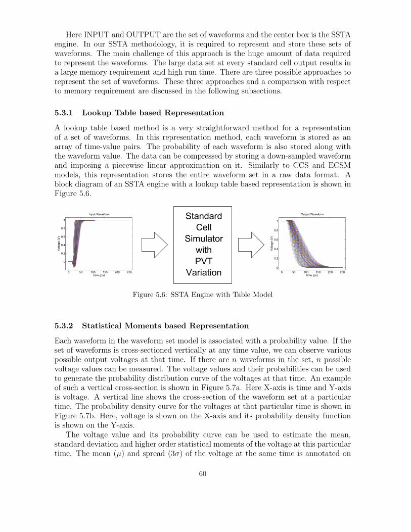
Here INPUT and OUTPUT are the set of waveforms and the center box is the SSTAengine. In our SSTA methodology, it is required to represent and store these sets ofwaveforms. The main challenge of this approach is the huge amount of data requiredto represent the waveforms. The large data set at every standard cell output results ina large memory requirement and high run time. There are three possible approaches torepresent the set of waveforms. These three approaches and a comparison with respectto memory requirement are discussed in the following subsections.
5.3.1 Lookup Table based Representation
A lookup table based method is a very straightforward method for a representationof a set of waveforms. In this representation method, each waveform is stored as anarray of time-value pairs. The probability of each waveform is also stored along withthe waveform value. The data can be compressed by storing a down-sampled waveformand imposing a piecewise linear approximation on it. Similarly to CCS and ECSMmodels, this representation stores the entire waveform set in a raw data format. Ablock diagram of an SSTA engine with a lookup table based representation is shown inFigure 5.6.
Standard
Cell
Simulator
with
PVT
Variation0 50 100 150 200 250
0
0.2
0.4
0.6
0.8
1
time (ps)
Voltage (
V)
Input Waveform
0 50 100 150 200 250
0
0.2
0.4
0.6
0.8
1
time (ps)
Voltage (
V)
Output Waveform
Figure 5.6: SSTA Engine with Table Model
5.3.2 Statistical Moments based Representation
Each waveform in the waveform set model is associated with a probability value. If theset of waveforms is cross-sectioned vertically at any time value, we can observe variouspossible output voltages at that time. If there are n waveforms in the set, n possiblevoltage values can be measured. The voltage values and their probabilities can be usedto generate the probability distribution curve of the voltages at that time. An exampleof such a vertical cross-section is shown in Figure 5.7a. Here X-axis is time and Y-axisis voltage. A vertical line shows the cross-section of the waveform set at a particulartime. The probability density curve for the voltages at that particular time is shown inFigure 5.7b. Here, voltage is shown on the X-axis and its probability density functionis shown on the Y-axis.
The voltage value and its probability curve can be used to estimate the mean,standard deviation and higher order statistical moments of the voltage at this particulartime. The mean (µ) and spread (3σ) of the voltage at the same time is annotated on
60

0 50 100 150 200 250
0
0.2
0.4
0.6
0.8
1
time (ps)
Vol
tage
(V
)
Waveform cut at time (t) = 77.0008 ps
signal at t
(a) The Set of Waveforms
0.1 0.2 0.3 0.4 0.5 0.6 0.7
0
1
2
3
4
Voltage (V)
Voltage pdf for waveform cut at time (t) = 77.0008 ps
pdf at t
(b) Probability of Voltage
Figure 5.7: Vertical cross-section of Waveforms at time t
the waveform set as shown in Figure 5.8a. Here the centre horizontal line correspondsto the mean and the top and the bottom lines represent the ±3σ bound of the voltageat this time. Annotation of the same µ and ±3σ on the probability density curve areshown in Figure 5.8b. Here the centre vertical line corresponds to the mean and the
61

0 50 100 150 200 250
0
0.2
0.4
0.6
0.8
1
time (ps)
Vol
tage
(V
)
Waveform cut at time (t) = 77.0008 ps
signal at tµ at t± 3σ at t
(a) The Set of Waveforms
0.1 0.2 0.3 0.4 0.5 0.6 0.7
0
1
2
3
4
Voltage (V)
Voltage pdf for waveform cut at time (t) = 77.0008 ps
pdf at tµ at t± 3σ at t
(b) Probability of Voltage
Figure 5.8: Vertical cross-section of Waveforms at time t with µ and ±σ of voltage
right and the left lines represent the ±3σ bound of the voltage at this time.The same process can be repeated for the entire time axis. This results into the
statistical moments of the voltage as a function of time. The first four moments,Mean (µ), Standard Deviation (σ), Skewness (γ), and Kurtosis (κ), of the voltage as a
62

0 50 100 150 200 250
0
0.2
0.4
0.6
0.8
1
time (ps)
Vol
tage
Mea
n (µ
) (V
)
Waveform Mean (µ)
(a) Mean (µ(t)) of waveform set
0 50 100 150 200 250
0
0.02
0.04
0.06
0.08
time (ps)
Vol
tage
Spr
ead
(σ)
(V)
Waveform Spread (σ)
(b) Standard Deviation (σ(t)) of waveform set
0 50 100 150 200 250
−5
−4
−3
−2
−1
0
1x 10
−4
time (ps)
Vol
tage
Ske
wne
ss (γ
)
Waveform Skewness (γ)
(c) Skewness (γ(t)) of waveform set
0 50 100 150 200 250
0
0.5
1
1.5
2
2.5
x 10−4
time (ps)
Vol
tage
Kur
tosi
s (κ
)
Waveform Kurtosis (κ)
(d) Kurtosis (κ(t)) of waveform set
Figure 5.9: First four moments of the waveform set as a function of time
function of the time are shown in Figure 5.9a, Figure 5.9b, Figure 5.9c, and Figure 5.9drespectively. In these figures, time is on the X-axis and the respective moments are onthe Y-axis.
Instead of storing the entire waveform set and the corresponding probability values,only the moment curves just described can be stored. The amount of higher ordermoment curves depends on the SSTA engine and its requirements. As compared tothe lookup table based method, this approach requires much less memory, as only fewcurves are sufficient to store the entire waveform set. The block diagram of an SSTAengine using a statistical moments based representation is shown in Figure 5.10. Herewe assume that only the first two moments (µ and σ) are required for the SSTA engine.
5.3.3 Pseudo Circuit based Representation
In SSTA, we need to store the set of output waveforms of any standard cell. Thus, aset of waveforms can be represented by a circuit with the PVT variation in it. Having
63

Standard
Cell
Simulator
with
PVT
Variation
0 50 100 150 200 250
0
0.2
0.4
0.6
0.8
1
time (ps)
Vo
lta
ge M
ea
n (µ
) (V
)
Waveform Mean (µ)
0 50 100 150 200 250
0
0.05
0.1
0.15
time (ps)
Vo
lta
ge S
pre
ad
(σ
) (V
)
Waveform Spread (σ)
0 50 100 150 200 250
0
0.2
0.4
0.6
0.8
1
time (ps)
Vo
lta
ge M
ea
n (µ
) (V
)
Waveform Mean (µ)
0 50 100 150 200 250
0
0.02
0.04
0.06
0.08
time (ps)
Vo
lta
ge S
pre
ad
(σ
) (V
)
Waveform Spread (σ)
Figure 5.10: SSTA Engine with Moment Model
the circuit and its PVT variations is sufficient to regenerate the voltage waveforms.We learned in Chapter 2 that the SSTA methodology may be used to estimate the
path delay in a digital circuit. Since SSTA is a stage-by-stage approach, the signal ateach node is mainly influenced by the part of the circuit between the start point of thedata path and that node. An example of a data path is depicted in Figure 5.11. Here,the signal at the second input of the gate g2 depends on the circuit components fromthe input of the DFF2 up to the interconnect n7.
Figure 5.11: Example path for SSTA
In this example, instead of storing the entire circuit up to interconnect n7, a referencecircuit can be used. This reference circuit can be use to regenerate the similar outputwaveform. This reference circuit will act as a pseudo circuit for everything up to theinput of the gate g2. The block diagram of an SSTA engine with this pseudo circuitbased representation is shown in Figure 5.12.
Here, the input signals of the gate are replaced by pseudo circuits. Since the MOD-ERN project is a using fast SPICE like simulation, this pseudo circuit will be mergedwith the standard cell circuit during simulation. Thus, the input waveforms are regen-erated while doing SSTA.
The proposed idea is to use one pseudo circuit with few parameters associated withit. Since the pseudo circuit is fixed by only a few parameters instead of the entire
64

Standard
Cell
Simulator
with
PVT
Variation
Output
Pseudo
Circuit
Input
Pseudo
Circuit
Output
Pseudo
Circuit
Input
Pseudo
Circuit
Figure 5.12: SSTA Engine with Pseudo Circuit Model
waveform set and their probabilities, it is a very compact model and able to regeneratea similar set of waveforms as needed at the input of the following standard cell.
5.4 Comparison of various Waveform Set Representations
As discussed in Section 5.3, there are three possible approaches to represent a set ofwaveforms, namely: lookup table, statistical moments, and pseudo circuit based repre-sentation. In the lookup table based approach, the complete waveform set along withtheir probability density is stored in the lookup table. Considering the large numberof waveforms, a very large memory space is required. In the statistical moments basedapproach, the statistical moments as a function of time are stored. This approach re-quires a smaller memory space. The SSTA engine in the MODERN project requireshigher order statistical moments of the waveforms. The need of higher order momentsincreases the memory requirement. In the pseudo circuit based approach, a pseudo cir-cuit is used to regenerate the waveform set similarly to the expected waveform set at theinput of standard cell during SSTA. A standard reference circuit with few parametersis used to model the pseudo circuit. Due to the very small number of parameters, thepseudo circuit representation is the most compact modeling approach among the threeproposed approaches. The details of the pseudo circuit will be discussed in Chapter 6.
5.5 Summary
Similar to the development of the waveform based model from the point based modelin STA, there is a need to have a waveform based uncertainty representation in SSTA.Therefore, the MODERN project is preserving various possible output waveforms dueto PVT variations at each node. This is called “a set of waveforms”. The concept ofthe set of waveforms and the uncertainty representation with it are discussed in thischapter. There are three possible methods to represent the set of waveforms in SSTAmethodology, namely a lookup table based representation, a statistical moments basedrepresentation and a pseudo circuit based representation. The pseudo circuit basedrepresentation turns out to be the most compact model because the set of waveformscan be regenerated using a reference circuit with only a few parameters in it. Theproposed pseudo circuit is discussed in Chapter 6.
65

66

Pseudo Circuit Model 6As discussed in Chapter 5, the pseudo circuit based representation for the set of wave-forms is the most compact model among the three proposed models. Additionally,the pseudo circuit model can be efficiently integrated with the SSTA engine used inthe MODERN project. In this chapter, the concept of the pseudo circuit, its inte-gration with the SSTA engine of the MODERN project, the approach and challengesfor the pseudo circuit modelling, a waveform comparison methodology and results arediscussed.
The organization of the chapter is as follows: the waveform set, pseudo circuit, andits integration with SSTA engine is discussed in Section 6.1. The proposed pseudocircuit and the simulation database required for waveform comparison are described inSection 6.2. Furthermore, the proposed waveform comparison methodology with an ex-ample is described in Section 6.3. The results of the pseudo circuit model are presentedin Section 6.4. At the end, a summary of the chapter is presented in Section 6.5.
6.1 Pseudo Circuit, Waveform Set and SSTA Engine
In the SSTA engine of the MODERN project, each input of a gate is a set of waveforms.This set of waveforms can be represented in various ways (see Chapter 5), and thepseudo circuit based representation turns out to be the most compact approach topreserve the set of waveforms. The main purpose of the pseudo circuit is to reconstructthe desired set of waveforms at the input of the standard cell. The SSTA engine inthe MODERN project will estimate the delay variation of each gate by simulating thecircuit of the gate. The simulation of the pseudo circuit can be carried out along withthe gate circuit for reconstruction of the waveforms. Therefore, the pseudo circuit needsto merge with the gate circuit while estimating the delay of the gate.
6.2 The Pseudo Circuit Model
The pseudo circuit model can be divided into two parts. First, we look at the selection ofthe pseudo circuit and its simulation using Spectre simulator to evaluate the accuracyand efficiency of the pseudo circuit model, which could be embedded to MODERNproject. Second, we study processing of the simulation output and constructing adatabase such that the waveforms can be compared. These two parts of the pseudocircuit model are discussed in the following subsections.
67

6.2.1 The Pseudo Circuit
The design space of the pseudo circuit is large because it has a very high degree offreedom in the circuit selection. Since the pseudo circuit is not a part of the real digitalcircuit which needs to be fabricated, some non trivial circuits can also be selected forthe design. This further increases the design space of the problem. There are fiveconstraints imposed on the pseudo circuit:
1. The output of the pseudo circuit should be similar to the output of a gate in thedigital circuit.
2. The pseudo circuit should be small.
3. The output space of the pseudo circuit should cover the entire possible outputrange of gates.
4. The absolute transition time of the waveform should match.
5. The pseudo circuit should have PVT variations.
The pseudo circuit will be developed while addressing the constraints mentionedabove. First, the output of the pseudo circuit should be similar to the output of thedigital circuits. This constraint is required to ensure that the reconstructed waveformsat the input of the gates are similar to the expected input waveforms. The outputsignal transition of a gate can be explained by charging or discharging of the effectivecapacitive load at the output pin of the gate. Therefore, an RC circuit is one of thesimplest possible pseudo circuits. However a small digital gate can generate a moreaccurate waveform than an RC circuit. Since the accuracy in the delay estimation isthe primary objective of the MODERN project, a digital gate is selected for the pseudocircuit design.
The pseudo circuit is included during simulation of each gate. Therefore, constrain-ing the size of the small circuit will help to ensure a low overhead on the simulation runtime. The smallest digital circuit is an inverter. Therefore, an inverter can be selectedas a pseudo circuit. As discussed in Chapter 5, the set of waveforms at the output ofan inverter chain is more realistic than at the output of a single inverter. Therefore,an inverter chain with three inverters is selected as a pseudo circuit. An inverter chainwith three inverters is shown in Figure 6.1. Here Inv1, Inv2 and Inv3 are the threeinverters of the inverter chain.
Inv1 Inv2 Inv3
Figure 6.1: An inverter chain with three inverters
The pseudo circuit will be used to represent any possible target waveform set. Thistarget waveform set could be output of any digital cell in the design. Therefore, as
68

mentioned in the third constraint, the pseudo circuit must be able to generate all suchpossible sets of waveforms. Quantitative measurement of the waveform set to ensure itsfull coverage is very complex due to the large number of waveforms. At this stage of thedevelopment, only the nominal waveform is considered for quantitative measurementto reduce the complexity of the problem. The nominal waveform is the output of thecircuit when all the PVT parameters are at their nominal values. The pseudo circuitshould be able to generate all possible nominal waveforms. A single waveform can bequalitatively measured by its slew. Therefore, it can be said that the nominal waveformof the pseudo circuit should be able to ensure the coverage of all possible slew values inthe digital circuit. As we know, the output of a gate primarily depends on two externalparameters, input signal slew and effective output capacitive load (see Chapter 2). Thepseudo circuit should have input signal slew (Sin) and output effective capacitive load(Cload) as two parameters of the pseudo circuit. An ideal ramp voltage source and acapacitive load are added in the pseudo circuit as shown in Figure 6.2.
Inv1 Inv2 Inv3
Cload
Sin
Figure 6.2: Inverter chain with input source and output load
The circuit shown in Figure 6.2 has one limitation. The output load of Inv1 andInv2 is not varying. For a constant capacitive load, the sensitivity of the output signalslew with respect to the input signal slew is very low for a digital circuit. Due to thisphenomenon, the variation of the signal slew at the input of Inv1 is not completelyreflected to the input of Inv2. Due to a similar phenomenon, the input signal slew ofInv3 is almost constant. It means that the input signal slew of Inv3 is not controllablein this circuit. It has been discussed earlier that the pseudo circuit should be able togenerate all possible nominal waveforms. Furthermore, the output of a gate dependson the input signal slew and effective output capacitive load. However, in this pseudocircuit, the input signal slew of Inv3 is not controllable. This limits the generationof all possible waveforms. The problem is addressed by adding additional capacitorsat each intermediate node between the inverters. The signal slew at the input ofeach inverter can be controlled by varying the value of the capacitor. Therefore, boththe input signal slew and the intermediate capacitor value will change together. Twoindependent capacitance values increase the design space by two dimensions. However,the exactly same capacitance value (Cin) for these intermediate capacitors can reducethe design space by one dimension while keeping full control on the output capacitanceof Inv2. Therefore, the same capacitance value (Cin) for these intermediate capacitorsis used. For each pair of Sin and Cload, the value of Cin is selected such that the inputsignal slew of Inv3 is exactly same as the input slew of Inv1. The modified circuit isshown in Figure 6.3.
69

Inv1 Inv2 Inv3
Cload
Sin
CinCin
Figure 6.3: Inverter chain with capacitors at internal nodes
The absolute start time of the transition of the output waveform in the circuit shownin Figure 6.3 strongly depends on the start time of the transition of the input signal.The target waveform set does not necessarily have the same start time of transition.Therefore, the fourth constraint is required. The synchronization of the target waveformwith the output of pseudo circuit is achieved by delaying the transition of the inputramp signal in the pseudo circuit. The delay in the voltage source is incorporated byintroducing a parameter for the signal offset in the voltage source as shown in Figure 6.4.This time is called as Tstart.
Inv1 Inv2 Inv3
Cload
Sin
CinCinTstart
Figure 6.4: Inverter chain with time offset
Now, the circuit shown in Figure 6.4 is capable of generating all possible nominaloutput waveforms. This circuit has four parameters: input signal slew, output capaci-tive load, internal capacitors, and start time of the ramp signal. However, the value ofinternal capacitors are dependent on the input signal slew and output capacitive load.Therefore, the circuit has only three independent parameters.
The fifth constraint for the pseudo circuit design is that it must have PVT vari-ations. This constraint is needed to generate variation in the waveforms. Since thePVT variations have many parameters, the selection of the parameters for the PVTvariation has a very high degree of freedom. The intuitive approach would be to addvariations in all the parameters because this scenario will increase the accuracy of thevariations in the output waveforms. However, the complexity of the simulation runwill increase. Additionally, the required iterations for the circuit simulation will in-crease exponentially. Therefore, only one parameter variation is selected to representthe variation in the pseudo circuit. This choice increases the simulation run time at thecost of limited variations in the output waveforms. In this phase of the developmentof the pseudo circuit model, such approximations are very useful for the analysis ofthe model. However, in future work, multiple parameters can be considered to increasethe accuracy. In this pseudo circuit, the channel length of both the PMOS (Lp) and
70

the NMOS (Ln) in the last inverter of the inverter chain is considered to have processvariations. The channel lengths Ln and Lp are assumed to have a correlation equalto one. The variation in the channel length is represented by its standard deviation(σL). The complete pseudo circuit is shown in Figure 6.5 and the circuit parametersare reported in Table 6.1.
Inv1 Inv2 Inv3
Cload
Sin
CinCinTstart
Ln / Lp
Figure 6.5: The Pseudo Circuit Schematic
Table 6.1: The Pseudo Circuit
Name Description
Circuit Inverter chain with three inverters and capacitive load at each node
Input Signal Ideal Ramp
Output Load Capacitive Load
Sweep Input Slew and Output Capacitive Load
Variations Channel length in last inverter
Starting Time Based on the transition time of the target waveform
The final pseudo circuit has four independent parameters and one dependent param-eter. The names of all the parameters, their range and the sizes of the MOSFETs aregiven in Table 6.2. These values are selected after various experiments while keepingthe design constraints in mind.
Table 6.2: Pseudo Circuit Parameters
Symbol Parameter Value / Range Remark
Sin Input Signal Slew [50 ps , 500 ps] Independent
Cload Output Capacitive Load [1 fF , 15 fF] Independent
Cin Internal Capacitive Load [0.1 fF , 14 fF] Dependent
σL Spread of Channel Length [3.33% , 16.67%] Independent
Tstart Offset in input signal 0 , > 0 Independent
Ln / Wn NMOS length and width 100 nm / 90 nm Fix
Lp / Wp PMOS length and width 100 nm / 135 nm Fix
The spread in the channel length (σL) directly controls the spread in the outputwaveform. Therefore, the channel length spread (σL) can attain various possible valuesin the specified range to generate various possible target waveform sets. Multiplesimulations of the pseudo circuit are needed to cover the entire range of σL, whichresults in very high run time. This problem is addressed by using the proposed method
71

of Fast Statistical Moment Estimation (FSME) (see Chapter 4). The FSME methodgives the flexibility to select the pdf of the parameters after the circuit simulation. Dueto this feature, the pseudo circuit is simulated only once with the maximum possibleparameter spread (σL) and the output is stored in a database. The actual spread ofthe channel length variation is used during waveform comparison. The FSME methodreduces the rerun of the circuit simulation for various possible values of σL.
The pseudo circuit is simulated for the sampled values of Sin and Cload from theirrespective range using the highest value of σL in the specified range. The outputwaveforms of each simulation along with their circuit configurations are stored in adatabase. This database is used during the SSTA flow to estimate the pseudo circuitparameters such that the target waveforms can be generated. The simulation outputand its structure in the database are given in Table 6.3. Here index i is used for inputslew, j for output load, k for the time, and l for simulation iteration due to uniformsampling of the channel length as given in FSME method.
Table 6.3: Simulation output in database
Sampled Data Function Remark
Sin[i] Sin Input Slew
Cload[j] Cload Output Load
Cin[i, j] Cin(Sin, Cload) Internal Capacitor
Wave[i, j, k, l] Wave(Sin, Cload, t, σL) Waveform Output
6.2.2 Database processing for waveform comparison
The comparison of the waveform sets is in itself a very challenging task due to thefact that a waveform set is a dataset with five dimensions (Sin, Cload, t, σL, V oltage).To reduce the complexity of the problem, only mean and standard deviation curves ofthe waveforms are compared. Additionally, instead of comparing the entire mean andstandard deviation curve, only their quality factors are compared. Here, quality factorsare the specific parameters which can quantitatively measure the shape of waveforms.Various possible quality factors have been analysed to compare mean and standarddeviation curves. Since we have four independent parameters in the pseudo circuit, atleast four quality factors are required to estimate these independent parameters. Theselected quality factors of the mean and standard deviation curves are discussed below.
1. The slew of the mean curve (QSlew)
2. The separation of mean and standard deviation curves (QShiftMean)
3. The peak height of the standard deviation curve (QMax)
4. The VDD / 2 crossing time of the mean curve (QTmid)
Here the prefix Q stands for quality factor. The quality factors are demonstratedwith an example of the mean and standard deviation curve in Figure 6.6. The detailsof the quality factors are discussed below using a set of waveforms. The notations of
72

the mean and standard deviation curves of the waveform set used in this illustrationare given in Table 6.4. Here k and l are the integral index of the sampled array of thecontinuous functions.
200 300 400 500 600
0
0.2
0.4
0.6
0.8
1
time (ps)
Mean (
µ)
(V)
200 300 400 500 600
0
10
20
30
40
time (ps)
Spre
ad (
σ)
(mV
)
QShiftMean
QSlewQMax
QTmid
Figure 6.6: Quality factors for the waveform comparison
Table 6.4: Mean and SD curves for quality factor illustration
Sampled Data Function Remark
M [k, l] Mean(t, σL) Waveform Mean
S[k, l] Sigma(t, σL) Waveform Standard Deviation
MU [k] MaxMean(t) Waveform Mean with maximum spread
SD[k] MaxSigma(t) Waveform SD with maximum spread
T [k] t time
The total number of samples in the time axis, i.e. the length of the vector T [k] is n.
n = length(T ) (6.1)
QSlew is the slew of the mean curve of the waveform set. Since the effect of thepositive and negative variation in the channel length are opposite, it keeps the nominal
73

and mean curve very close to each other. Therefore the QSlew of the mean curve due tovarious values of σL remains consistent. In the waveform comparison methodology, theslew of the mean curve due to maximum spread (MU [k]) is used to define the QSlew
of the set of waveforms. Therefore, the QSlew is independent of the spread used in thepseudo circuit.
Mathematically, QSlew can be define as follows:
QSlew = |t90 − t10| (6.2)
Here, t10 and t90 are the 10% and 90% voltage crossing time of MU [k] respectively.The crossing time t10 and t90 can be defined as follows:
t10 = t such that MaxMean(t) = 0.1× VDD (6.3)
t90 = t such that MaxMean(t) = 0.9× VDD (6.4)
QShiftMean is a measure of separation between mean and standard deviation curves.The position of the mean curve is defined by its 50% voltage crossing time. Similarto QSlew, the mean curve due to maximum spread in the channel length is used todefine the position of the mean curve. The position of the standard deviation curve isdefined by the weighted mean of time while considering the standard deviation curveas a weight profile. The weight of a sampled time can be estimated by integratingthe weight profile. Since the standard deviation of the output waveform is directlyproportional to the spread of the channel length, the weighted mean of time doesnot change due to change in the spread of the channel length. Therefore, the standarddeviation curve due to maximum spread is used to measure the position of the standarddeviation curve.
Mathematically, QShiftMean can be defined as follows:
QShiftMean = tsd − tmu (6.5)
Here, tsd and tmu are the positions of the SD[k] and MU [k] curves respectively. Theposition of MU [k] can be defined as follows:
tmu = t such that MaxMean(t) = 0.5× VDD (6.6)
Here, tmu is the 50% voltage crossing time of MU [k]. The position of SD[k] can bedefined as follows:
tsd =
∑
k(T [k]×W [k])∑
k W [k](6.7)
Here, tsd is the weighted sum of time (T [k]) with its weight W [k]. Since SD[k] isthe weight profile of time (T [k]), weight (W [k]) can be calculated by integrating theweight profile (SD[k]) in the adjacent non-overlapping windows (local windows) atevery sampled time. If MaxSigma(t) is the weight profile function, then MaxSigma(t)and SD[k) can be related as:
SD[k] = MaxSigma(T [k]) (6.8)
74

Here, SD[k] contains the sampled values of the continuous function MaxSigma(t).Now, if the lower bound of the local window for T [k] is tl[k] and the upper bound isth[k], then the weight of time T [k] can be define as:
W [k] =
∫ th[k]
tl[k]
MaxSigma(t)dt (6.9)
Integration is a compute intensive process. Therefore, a piecewise constant ap-proximation is used to speedup the integration for calculation of weight (W [k]). Themodified equation with piecewise constant approximation is given below:
W [k] = SD[k]× (th[k]− tl[k]) (6.10)
⇒ W [k] = SD[k]×∆T [k] (6.11)
Here, ∆T [k] is the length of the local window around the time sample T [k]. The lowerand upper bound of this local window can be calculated as follows:
tl[k] =
{
T [1]− T [2]−T [1]2
if k = 1T [k−1]+T [k]
2if k 6= 1
(6.12)
and
th[k] =
{ T [k]+T [k+1]2
if k 6= n
T [n] + T [n]−T [n−1]2
if k = n(6.13)
Therefore, ∆T [k] can be define as:
∆T [k] = th[k]− tl[k] (6.14)
⇒ ∆T [k] =
t[2]− t[1] if k = 1t[k+1]−t[k−1]
2if k 6= 1&k 6= n
t[n]− t[n− 1] if k = n(6.15)
QMax is the maximum spread of the waveform. Since the spread in the outputwaveform is directly proportional to the spread of the channel length (σL), QMax is afunction of σL. For each value of the spread, QMax is defined as:
QMax(σL) = Max(Sigma(t, σL)) (6.16)
QMax on the sampled database can be designed as follows:
QMax[l] = Max(S[k, l]) (6.17)
During the experiments, it has been found that QMax is a linear function of σL. There-fore, QMax can be decomposed as follows:
QMax = QMaxM × σL +QMaxC (6.18)
Here, QMaxM is the slope of the line and QMaxC is the intersection of line with theQMax axis.
75

QTmid is the 50% voltage crossing time of the mean curve. QTmid is the same asTmu in (6.6) which is redefined as
QTmid = t such that MaxMean(t) = 0.5× VDD (6.19)
This parameter is used to measure the absolute start time of the transition of thewaveform set. The database of the simulation outputs of the pseudo circuit is generatedwith Tstart equal to zero.
Tstart = 0 for pseudo circuit database (6.20)
Therefore, QTmid corresponds to Tstart = 0. The difference in the absolute starttime of the transition in the target waveform set is compensated by changing the Tstart
parameter of the pseudo circuit model which will be used in the SSTA flow.The quality factors of one set of waveforms are discussed here. However, the sim-
ulation database has waveforms for each pair of input signal slew (Sin) and outputcapacitive load (Cload). Therefore the quality factors are calculated for each pair of Sin
and Cload. The extended structure of the database is given in Table 6.5. Index i is usedfor input slew, j for output load, k for the time, and l for simulation iteration due toprocess variation.
Table 6.5: Database Structure
Sampled Data Function Remark
Sin[i] Sin Input slew
Cload[j] Cload Output load
Cin[i, j] Cin(Sin, Cload) Internal capacitor
T [k] t Time
Wave[i, j, k, l] Wave(Sin, Cload, t, σL) Waveform output
QSlew[i, j] QSlew(Sin, Cload) Slew of mean curve
QShiftMean[i, j] QShiftMean(Sin, Cload) Separation of mean and sigma curve
QMaxM [i, j, l] QMaxM(Sin, Cload, σL) Peak of sigma curve
QMaxM [i, j] QMaxM(Sin, Cload) Slope of the QMax vs σLQMaxC [i, j] QMaxC(Sin, Cload) QMax axis intersection of QMax vs σLQTmid[i, j] QTmid(Sin, Cload) VDD/2 crossing time of mean curve
6.3 Waveform Comparison Methodology
A database of the pseudo circuit simulation outputs and a targeted waveform set arethe input for the pseudo circuit model generation flow. The generated pseudo circuitfrom this flow can be used by the SSTA engine to reconstruct the target waveformset at the input of the gate. It is discussed earlier in this chapter that the outputwaveform of the pseudo circuit should closely match with the target waveform. It hasalso been discussed that the quality factors will be used to estimate the configurationof the pseudo circuit. The quality factors and circuit parameters are given below:
76

• Quality Factor
1. QSlew
2. QShiftMean
3. QMax
4. QTmid
• Circuit Parameters
1. Sin
2. Cload
3. Cin
4. σL
5. Tstart
The quality factors of the targeted waveform set are calculated first. Let us namethem TSlew, TShiftMean, TMax, and TTmid. Here the prefix T stands for target waveform.The methodology to match the quality factors and circuit parameter estimation isillustrated with an example.
A target waveform set, its mean and standard deviation curves are shown in Fig-ure 6.7 and the quality factors are reported in Table 6.6.
Table 6.6: Quality factors of target waveform
Quality Factor Value
TSlew 76.1 ps
TShiftMean 9.7 ps
TMax 89.6 mV
TTmid 307.0 ps
The quality factor QSlew of the database is a three dimensional dataset of the slewof the mean curve of the waveforms for each pair of input signal slew (Sin) and outputcapacitive load (Cload) as shown in Figure 6.8a. In this figure Cload is on the X-axis, Sin
is on the Y-axis, and QSlew is on the Z-axis. Each node of the plane is the QSlew due tocorresponding pair of Sin and Cload. The target slew (TSlew) can also be represented ina three dimensional space using a plane parallel to the Sin-Cload plane. Both the QSlew
and TSlew planes are shown in Figure 6.8b.Since the TSlew plane is parallel to the Sin-Cload plane, the intersection line of QSlew
and TSlew planes will be a line in a two dimensional space of Sin-Cload as shown inFigure 6.8c. In this figure, Cload is on the X-axis and Sin is on the Y-axis. The redpoints in this figure are the intersection points of two planes. These points are estimatedwith the help of a numerical analysis method. The black line is a linear best fit curveof the intersection points. The linear relation of Sin and Cload for this intersection lineis given in the title of the figure. Each point in this line can generate a configurationof the pseudo circuit which will produce the QSlew equal to TSlew.
77

0 200 400 600
0
0.2
0.4
0.6
0.8
1
time (ps)V
olta
ge (
V)
Target Waveform Set
(a) Target Set of Waveforms
0 200 400 600
0
0.2
0.4
0.6
0.8
1
time (ps)
Vol
tage
(V
)
Target Waveform Mean Curve
(b) Mean Curve
0 200 400 600
0
20
40
60
80
time (ps)
Vol
tage
(m
V)
Target Waveform Spread Curve
(c) Standard Deviation Curve
Figure 6.7: Target Waveform Set
Similar to QSlew, QShiftMean is also a three dimensional dataset of the separationbetween mean curve and standard deviation curve of the waveform set for each pair ofCin and Cload as shown in Figure 6.9a. In this figure, Cload is on the X-axis, Sin is onthe Y-axis, and QShiftMean is on the Z-axis. Each node of the plane is the QShiftMean
due to corresponding pair of Sin and Cload. The target separation between mean andstandard deviation curve (TShiftMean) can also be represented in a three dimensionalspace using a plane parallel to the Sin-Cload plane. Both the QShiftMean and TShiftMean
planes are shown in Figure 6.9b.
Similar to the TSlew plane, the TShiftMean plane is also parallel to the Sin-Cload plane,its intersection with QShiftMean plane will be a line in a two dimensional space of Sin-Cload as shown in Figure 6.9c. In this figure, Cload is on the X-axis and Sin is on theY-axis. The red points in this figure are the intersection points of two planes. Thesepoints are estimated with the help of a numerical analysis method. The black line isa linear best fit curve of the intersection points. The linear relation of Sin and Cload
for this intersection line is given in the title of the figure. Each point in this line can
78

510
15
100200
300400
500
100
200
300
400
Cload
(fF)
QSlew
vs Sin
vs Cload
Sin
(ps)
QS
lew (
ps)
(a) QSlew vs Sin vs Cload
510
15
100200
300400
500
100
200
300
400
Cload
(fF)
QSlew
= 76.0757 ps
Sin
(ps)
QS
lew (
ps)
(b) QSlew and TSlew Planes
2 4 6 8 10 12 14
100
200
300
400
500
Cload
(fF)
Sin
(ps
)
Sin
= −106.4519 Cload
+ (367.4132)
(c) Intersection of QSlew and TSlew Planes
Figure 6.8: Sin vs Cload intersaction line for QSlew equals to TSlew
79

generate a configuration of the pseudo circuit which will produce the QShiftMean equalto TShiftMean.
510
15
100200
300400
500
0
50
100
Cload
(fF)
QShiftMean
vs Sin
vs Cload
Sin
(ps)
QS
hiftM
ean (
ps)
(a) QShiftMean vs Sin vs Cload
510
15
100200
300400
500
0
50
100
Cload
(fF)
QShiftMean
= 9.6923 ps
Sin
(ps)
QS
hiftM
ean (
ps)
(b) QShiftMean and TShiftMean Planes
2 4 6 8 10 12 14
100
200
300
400
500
Cload
(fF)
Sin
(ps
)
Sin
= 204.0255 Cload
+ (−438.7114)
(c) Intersection of QShiftMean and TShiftMean Planes
Figure 6.9: Sin vs Cload intersaction line for QShiftMean equals to QShiftMean
80

The intersection of QSlew with TSlew and QShiftMean with TShiftMean gives two linesin the Sin-Cload plane which satisfy the individual quality factors. The intersection ofthese two lines will give a pair of Sin-Cload which will satisfy both the quality factorssimultaneously as shown in Figure 6.10. In this figure, the lines of Figure 6.8c andFigure 6.9c are plotted together. The intersection point is given in the title of the figure.Let us call the intersection value of Sin and Cload MSin and MCload respectively. Herethe prefix M stands for pseudo circuit model. These MSin and MCload are the twoparameters of the pseudo circuit which satisfy the quality factors TSlew and TShiftMean.
2 4 6 8 10 12 14
100
200
300
400
500
Cload
(fF)
Sin
(ps
)
MSin
= 91.0212 ps & MCload
= 2.5964 fF
Figure 6.10: Intersection of Slew and ShiftMean lines
The datasets Cin, QMaxM , QMaxC , and QTmid are a function of Sin and Cload asshown in Table 6.5. These functions are stored in the database using three dimensionalmatrix formats. The values of Cin, QMaxM , QMaxC , and QTmid for the correspondingmodel parameters MSin and MCload can be estimated using an interpolation function.Let us call these interpolated values MCin, MQMaxM , MQMaxC , and MTmid such that
MCin = Cin(MSin,MCload) (6.21)
MQMaxM = QMaxM(MSin,MCload) (6.22)
MQMaxC = QMaxC(MSin,MCload) (6.23)
MTmid = QTmid(MSin,MCload) (6.24)
As we discussed earlier, QMaxM and QMaxC are the coefficients of the linear functionof QMax vs σL. The equation is rewritten below.
QMax = QMaxM × σL +QMaxC (6.25)
The value of σL for the target TMax can be estimated using the following equation.Here the estimated value of σL is called MσL.
MσL =TMax −MQMaxC
MQMaxM
(6.26)
MσL = (TMax −MQMaxC)/MQMaxM (6.27)
81

The linear relation of QMax versus σL is plotted in Figure 6.11. Here, σL is on theX-axis and QMax is on the Y-axis. The values of TMax and MσL are given in the titleof the figure.
0 5 10 15 20
20
40
60
80
100
120
140
σL (nm)
QM
ax (
mV
)
TMax
= 89.7563mV and MσL = 11.9514nm
Figure 6.11: QMax vs σL
The 50% crossing time of the mean curve of the waveform set corresponding tothe selected MSin and MCload is MTmid. The same for the target waveform is TTmid.Since zero offset in the absolute starting time of the ideal ramp is used in the pseudocircuit, MTmid should be smaller than TTmid. The delay compensation, required for thesynchronization of the absolute time, is equal to the difference of the TTmid and MTmid.This time value is used to offset the start time of the input signal transition and calledMTstart.
MTstart = TTmid −MTmid (6.28)
The pseudo circuit configuration parameters for the target waveform are estimatedusing the methodology discussed above. The output of the pseudo circuit with thiscircuit configuration is expected to match the specified quality factors. However, thereis one problem which is not yet addressed. This is about the loading of the pseudo circuitby the standard cell in the design. This limitation is addressed by the compensationmethod discussed below.
Load Compensation During the pseudo circuit database generation, the pseudocircuit was loaded by the Cload only. Whereas, during the simulation of the pseudocircuit in the SSTA flow, the input impedance of the gate is added in parallel withCload. The extra load is compensated by reducing the Cload by the effective inputcapacitance of the standard cell.
Mathematically, the load compensation is described below. Let us say that TCload
is the effective input capacitive load of the standard cell. The MCload is reduced byTCload value to compensate the extra load due to the gate as follows:
MCload = MCload − TCload (6.29)
This ends the methodology for the waveform set comparison and selection of thepseudo circuit parameters. The list of all the pseudo circuit parameters with their
82
values is given in Table 6.7.
Table 6.7: Pseudo Circuit Parameters after waveform comparison methodology
Parameter Value Remark
MSin 91.0 ps Slew of the input ramp signal
MCload 2.6 fF Capacitive load of the pseudo circuit
MCin 1.7 fF Internal capacitive load of the inverters
MσL 12.0 nm Variation spread of the channel length
MTstart 47.6 ps Offset in the start time of the simulation
6.4 Results
Firstly, the output of the pseudo circuit model for the example target waveform setused in Section 6.3 will be discussed. Following this, results from various other sets ofwaveforms will be presented briefly.
The target set of waveforms shown in Figure 6.7 is used in the previous section todevelop the waveform comparison methodology. The quality factors corresponding tothe target waveform are given in Table 6.6 and the pseudo circuit parameters based onthe discussed waveform comparison methodology are given in Table 6.7.
The output of the pseudo circuit with estimated circuit parameters is generated. Thetarget set of waveforms is plotted in Figure 6.12a. The output of the pseudo circuitmodel output with corresponding pseudo circuit parameters is plotted in Figure 6.12b.Here time is on the X-axis and mean voltage (µ) in on the Y-axis. The output ofthe pseudo circuit model is called the model set of waveforms. It can be observedthat the target waveform set and model waveform set do not match exactly. Thisis primarily because only quality factors are compared to select the parameters ofpseudo circuit. Therefore, it is expected that the quality factors should match veryclosely. Furthermore, the mean curve and standard curve of these two waveform setsare expected to match closely, which is discussed further below.
The mean curve of the target waveform set and pseudo circuit model output areplotted in Figure 6.13a. Here time is on the X-axis and mean voltage (µ) in on theY-axis. The blue curve is the mean curve of the target waveform set and red curve isthe output of the pseudo circuit model. It can be seen that the output of the pseudocircuit model matches quite well. The error in the mean curve of the pseudo circuitwith respect to the mean curve of the target waveform set is plotted in Figure 6.13c.Here time is on the X-axis and error in the mean curve (εµ) is on the Y-axis. Thesupply voltage is used as a reference to calculate the error percentage of the differencein the mean curves, which is given as
εµ = 100×µT − µM
VDD(6.30)
Here, εµ is the error percentage and VDD is the supply voltage. The mean curve of thetarget waveforms is represented by µT and µM represents the mean curve of the pseudocircuit model waveforms. It can be seen that the error is within 1.6%.
83
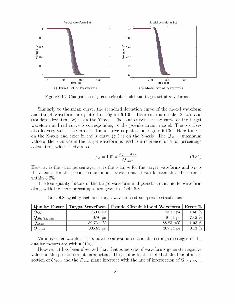
0 200 400 600
0
0.2
0.4
0.6
0.8
1
time (ps)
Vol
tage
(V
)
Target Waveform Set
(a) Target Set of Waveforms
0 200 400 600
0
0.2
0.4
0.6
0.8
1
time (ps)
Vol
tage
(V
)
Model Waveform Set
(b) Model Set of Waveforms
Figure 6.12: Comparison of pseudo circuit model and target set of waveforms
Similarly to the mean curve, the standard deviation curve of the model waveformand target waveform are plotted in Figure 6.13b. Here time is on the X-axis andstandard deviation (σ) is on the Y-axis. The blue curve is the σ curve of the targetwaveform and red curve is corresponding to the pseudo circuit model. The σ curvesalso fit very well. The error in the σ curve is plotted in Figure 6.13d. Here time ison the X-axis and error in the σ curve (εσ) is on the Y-axis. The QMax (maximumvalue of the σ curve) in the target waveform is used as a reference for error percentagecalculation, which is given as
εσ = 100×σT − σM
QMax
(6.31)
Here, εσ is the error percentage, σT is the σ curve for the target waveforms and σM isthe σ curve for the pseudo circuit model waveforms. It can be seen that the error iswithin 8.2%.
The four quality factors of the target waveform and pseudo circuit model waveformalong with the error percentages are given in Table 6.8.
Table 6.8: Quality factors of target waveform set and pseudo circuit model
Quality Factor Target Waveform Pseudo Circuit Model Waveform Error %
QSlew 76.08 ps 74.82 ps 1.66 %
QShiftMean 9.70 ps 10.41 ps 7.42 %
QMax 89.76 mV 88.83 mV 1.03 %
QTmid 306.93 ps 307.34 ps 0.13 %
Various other waveform sets have been evaluated and the error percentages in thequality factors are within 10%.
However, it has been observed that that some sets of waveforms generate negativevalues of the pseudo circuit parameters. This is due to the fact that the line of inter-section of QSlew and the TSlew plane intersect with the line of intersection of QShiftMean
84

0 200 400 600
0
0.2
0.4
0.6
0.8
1
time (ps)
Vol
tage
(V
)
Target and Model Waveform Mean Curve
TargetModel
(a) Mean Curves (µM and µT )
0 200 400 600
0
20
40
60
80
time (ps)
Vol
tage
(m
V)
Target and Model Waveform Spread Curve
TargetModel
(b) Standard Deviation Curves (σM and σT )
0 200 400 600−1.5
−1
−0.5
0
0.5
1
1.5
time (ps)
Err
or (
%)
Error in Target vs Model (Mean Curve)
(c) Error in Mean Curves (εµ)
0 200 400 600−6
−4
−2
0
2
4
6
8
time (ps)
Err
or (
%)
Error in Target vs Model (Spread Curve)
(d) Error in Standard Deviation Curves (εσ)
Figure 6.13: Result comparison of pseudo circuit model and target waveform set
and TShiftMean in negative values of Sin or Cload (see Figure 6.10). The failing waveformsets are mainly the output of the standard cells where input signal slew or output loadis very low or very high. More investigation and development of the pseudo circuitmodel could be a possible extension of the presented work.
6.5 Summary
This chapter proposes a pseudo circuit model which can be used to reconstruct thetarget set of waveforms. The main components of the pseudo circuit are an inverterchain of three inverters with process variations in the last inverter, an ideal ramp voltagesource with variable start time of the signal transition, a capacitive load, and internalcapacitors. The pseudo circuit has four independent parameters and one dependentparameter. The rest of the circuit parameters are kept fixed.
The pseudo circuit is simulated with various circuit configurations of its parameters
85

and a database is built. The target waveform is compared with this database of thecollection of waveforms and the pseudo circuit model parameters are estimated. Sincethe set of waveforms contains a huge amount of data points, direct comparison is notpossible. Therefore, only a few quality factors of the mean and standard deviationcurves of the set of waveforms are compared. The pseudo circuit has four indepen-dent parameters, therefore four independent quality factors have been proposed for thecomparison.
The four quality factors, pseudo circuit database generation for quality factor com-parison, and the waveform comparison methodology are described in this chapter. Thecomplete flow of waveform comparison and pseudo circuit parameter estimation is il-lustrated with an example of the target waveform set.
The mean and standard deviation curves of the target waveform set and the outputof the pseudo circuit model are compared. The error between the quality factors ofboth waveform sets are within 7% in the given example. Various other target waveformsets have been used to generate the pseudo circuit model and the errors in the qualityfactors are within 10%. However, a few waveform sets generate negative pseudo circuitmodel. More investigation and development of the pseudo circuit model is required.
86

Conclusion 7After one year of hard and dedicated work, some progress has been made in the thesisproject. Summary and the future work related to this project are discussed here.
7.1 Summary
A detailed introduction about the state of the art in timing analysis methodologieshas been discussed in Chapter 2. Available circuit simulation and analysis tools andMOSFET models are also discussed there.
In Chapter 3, a discussion about the variation in the delay of the standard cellsdue to PVT variations with the help of the first two statistical moments (Mean andStandard Deviation) is presented. The standard cells in this analysis are taken fromthe 45nm PTM model based Nangate open cell library. It was found that the variationsin the channel length and channel width affect the variation of delay the most. Fur-thermore, the primary cause of the non-Gaussian distribution of the delay variation isdue to the inverse relation of the delay with the channel width. Higher orders of statis-tical moments (Skewness and Kurtosis) have been used to quantify the non-Gaussiandistributions.
In Chapter 4, a simulation and analysis method based on the uniform samplingtechnique and weighted sample estimator have been proposed, which require fewer sim-ulation runs for statistical moment estimation. The number of simulation iterationsrequired by this Fast Statistical Moment Estimation (FSME) method is at least twoorders of magnitude lower than the number of simulation runs required in the standardMonte Carlo method. Along with this, changes in parameter spread and/or probabilitydensity function do not require rerunning of the circuit simulations, which results intofaster run time and smaller memory requirement. State of the art industrial circuitsimulation tools can run Monte Carlo with Gaussian, lognormal and uniform distribu-tion only whereas any distribution can be used in the proposed method. Along withthis, two methods have been discussed to estimate the probability density of the simu-lation result. The probability density function of the standard cell output with differentprobability density functions of the input PVT parameters is also discussed.
The concept of the set of waveforms and its integration with the timing analysistool are presented in Chapter 5. The uncertainty representation with the set of wave-form with the help of simulated waveform sets are discussed here. Furthermore, threepossible methods of representation of the set of waveforms are developed and com-pared. These representation methods are based on lookup table, statistical momentsand pseudo circuits. The pseudo circuit based representation is the most compactmodelling approach among them.
The pseudo circuit based waveform set representation is developed in Chapter 6.
87

The requirements and constraints to develop the pseudo circuit model are discussedfirst. Followed by this, the pseudo circuit model is developed by addressing the designconstraints. Thereafter, waveform comparison methodology has been developed togenerate the pseudo circuit model for any given set of waveforms.
7.2 Future Work
The waveform set model has not been evaluated in detail for various possible waveformsets. The detailed evaluation of the performance and accuracy of the pseudo circuitmodel is a possible extension of the presented work. In this thesis work, Spectre isused to develop the pseudo circuit model. However, the application of this pseudocircuit model is within SSTA engine which does not have Spectre as a circuit simulatortool. Therefore, the performance and accuracy analysis of the proposed pseudo circuitmodel with the circuit simulation engine of the SSTA flow (e.g. fast circuit simulatordeveloped in the MODERN project) is also a possible extension to this work.
88
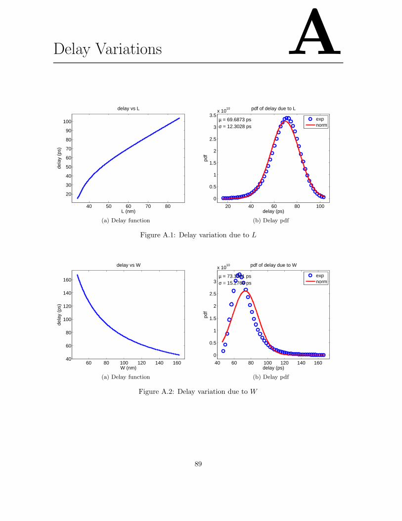
Delay Variations A
40 50 60 70 80
20
30
40
50
60
70
80
90
100
L (nm)
dela
y (p
s)
delay vs L
(a) Delay function
20 40 60 80 100
0
0.5
1
1.5
2
2.5
3
3.5x 10
10
delay (ps)pd
f
pdf of delay due to L
expnorm
µ = 69.6873 psσ = 12.3028 ps
(b) Delay pdf
Figure A.1: Delay variation due to L
60 80 100 120 140 16040
60
80
100
120
140
160
W (nm)
dela
y (p
s)
delay vs W
(a) Delay function
40 60 80 100 120 140 160
0
0.5
1
1.5
2
2.5
3
x 1010
delay (ps)
pdf of delay due to W
expnorm
µ = 73.1581 psσ = 15.2768 ps
(b) Delay pdf
Figure A.2: Delay variation due to W
89

440 460 480 500
64
66
68
70
72
74
76
78
Vth (mV)
dela
y (p
s)
delay vs Vth
(a) Delay function
65 70 75
0
2
4
6
8
10
12
14
16
x 1010
delay (ps)
pdf of delay due to Vth
expnorm
µ = 70.3635 psσ = 2.3767 ps
(b) Delay pdf
Figure A.3: Delay variation due to Vth
0.85 0.9 0.95 1 1.05 1.1 1.1560
65
70
75
80
85
VDD (V)
dela
y (p
s)
delay vs VDD
(a) Delay function
60 65 70 75 80 85
0
2
4
6
8
10
x 1010
delay (ps)
pdf of delay due to VDD
expnorm
µ = 70.7131 psσ = 4.1586 ps
(b) Delay pdf
Figure A.4: Delay variation due to VDD
90
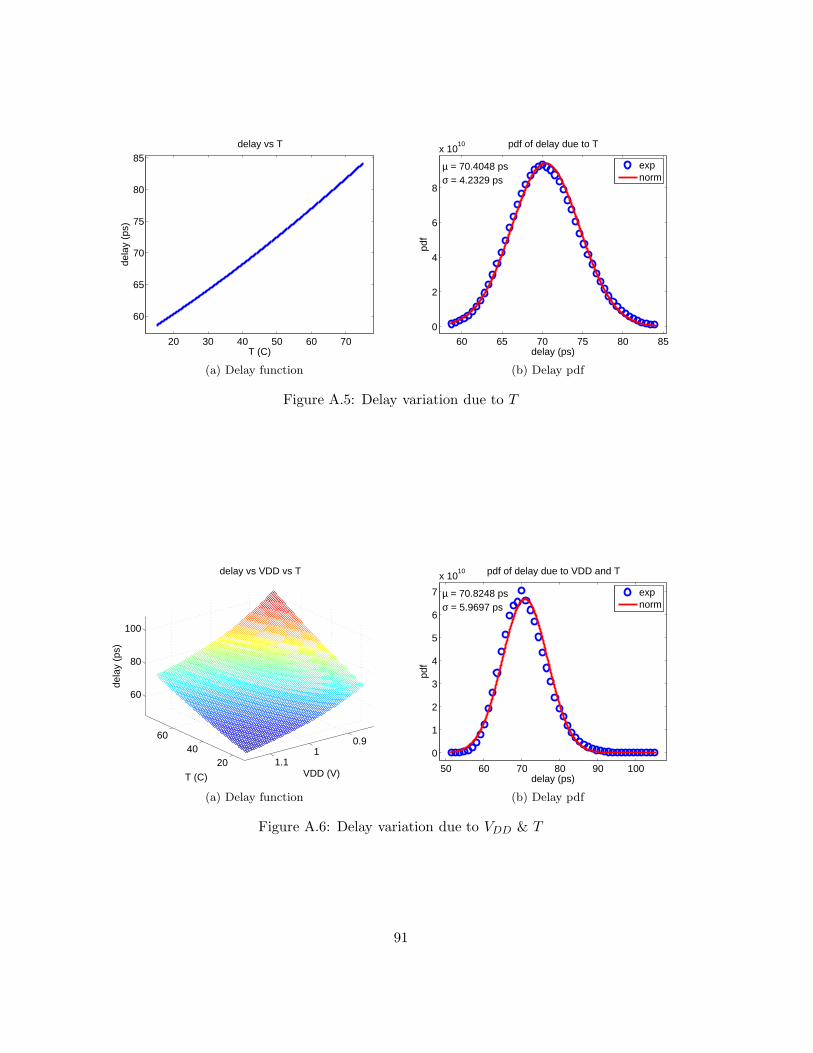
20 30 40 50 60 70
60
65
70
75
80
85
T (C)
dela
y (p
s)
delay vs T
(a) Delay function
60 65 70 75 80 85
0
2
4
6
8
x 1010
delay (ps)
pdf of delay due to T
expnorm
µ = 70.4048 psσ = 4.2329 ps
(b) Delay pdf
Figure A.5: Delay variation due to T
2040
600.9
11.1
60
80
100
VDD (V)
delay vs VDD vs T
T (C)
dela
y (p
s)
(a) Delay function
50 60 70 80 90 100
0
1
2
3
4
5
6
7
x 1010
delay (ps)
pdf of delay due to VDD and T
expnorm
µ = 70.8248 psσ = 5.9697 ps
(b) Delay pdf
Figure A.6: Delay variation due to VDD & T
91

440460
480500
0.91
1.1
60
70
80
90
100
VDD (V)
delay vs VDD vs Vth
Vth (mV)
dela
y (p
s)
(a) Delay function
60 70 80 90 100
0
2
4
6
8
x 1010
delay (ps)
pdf of delay due to VDD and Vth
expnorm
µ = 70.7863 psσ = 4.8487 ps
(b) Delay pdf
Figure A.7: Delay variation due to VDD & Vth
50100
150
0.91
1.1
50
100
150
W (nm)
delay vs VDD vs W
VDD (V)
dela
y (p
s)
(a) Delay function
50 100 150
0
0.5
1
1.5
2
2.5
3
x 1010
delay (ps)
pdf of delay due to VDD and W
expnorm
µ = 73.6044 psσ = 16.0376 ps
(b) Delay pdf
Figure A.8: Delay variation due to VDD & W
92
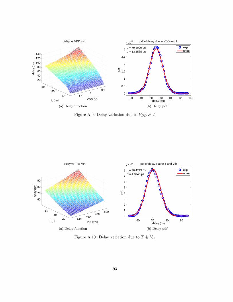
40
60
800.9
11.1
20
40
60
80
100
120
140
VDD (V)
delay vs VDD vs L
L (nm)
dela
y (p
s)
(a) Delay function
20 40 60 80 100 120 140
0
0.5
1
1.5
2
2.5
3
x 1010
delay (ps)
pdf of delay due to VDD and L
expnorm
µ = 70.1009 psσ = 13.1535 ps
(b) Delay pdf
Figure A.9: Delay variation due to VDD & L
440460
480500
2040
60
60
70
80
90
Vth (mV)
delay vs T vs Vth
T (C)
dela
y (p
s)
(a) Delay function
60 70 80 90
0
1
2
3
4
5
6
7
8
x 1010
delay (ps)
pdf of delay due to T and Vth
expnorm
µ = 70.4743 psσ = 4.8743 ps
(b) Delay pdf
Figure A.10: Delay variation due to T & Vth
93
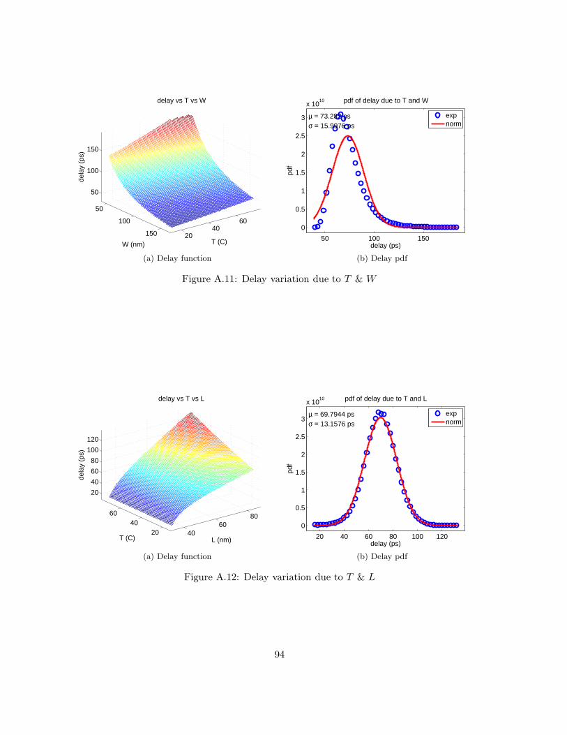
50
100
150 2040
60
50
100
150
T (C)
delay vs T vs W
W (nm)
dela
y (p
s)
(a) Delay function
50 100 150
0
0.5
1
1.5
2
2.5
3
x 1010
delay (ps)
pdf of delay due to T and W
expnorm
µ = 73.282 psσ = 15.9976 ps
(b) Delay pdf
Figure A.11: Delay variation due to T & W
4060
80
2040
60
20
40
60
80
100
120
L (nm)
delay vs T vs L
T (C)
dela
y (p
s)
(a) Delay function
20 40 60 80 100 120
0
0.5
1
1.5
2
2.5
3
x 1010
delay (ps)
pdf of delay due to T and L
expnorm
µ = 69.7944 psσ = 13.1576 ps
(b) Delay pdf
Figure A.12: Delay variation due to T & L
94

50
100
150 440460
480500
50
100
150
Vth (mV)
delay vs Vth vs W
W (nm)
dela
y (p
s)
(a) Delay function
50 100 150
0
0.5
1
1.5
2
2.5
3
x 1010
delay (ps)
pdf of delay due to Vth and W
expnorm
µ = 73.239 psσ = 15.5408 ps
(b) Delay pdf
Figure A.13: Delay variation due to Vth & W
4060
80
440460
480500
20
40
60
80
100
120
L (nm)
delay vs Vth vs L
Vth (mV)
dela
y (p
s)
(a) Delay function
20 40 60 80 100 120
0
0.5
1
1.5
2
2.5
3
x 1010
delay (ps)
pdf of delay due to Vth and L
expnorm
µ = 69.7535 psσ = 12.5846 ps
(b) Delay pdf
Figure A.14: Delay variation due to Vth & L
95
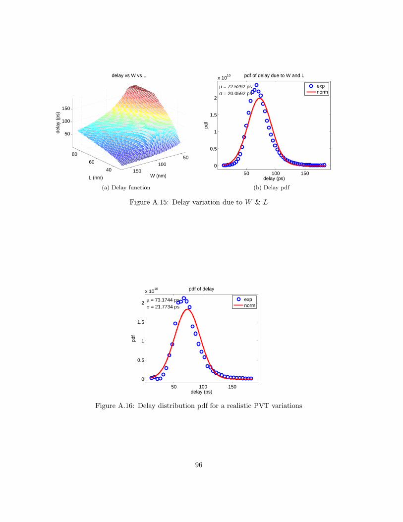
40
60
8050
100150
50
100
150
W (nm)
delay vs W vs L
L (nm)
dela
y (p
s)
(a) Delay function
50 100 150
0
0.5
1
1.5
2
x 1010
delay (ps)
pdf of delay due to W and L
expnorm
µ = 72.5292 psσ = 20.0592 ps
(b) Delay pdf
Figure A.15: Delay variation due to W & L
50 100 150
0
0.5
1
1.5
2
x 1010
delay (ps)
pdf of delay
expnorm
µ = 73.1744 psσ = 21.7734 ps
Figure A.16: Delay distribution pdf for a realistic PVT variations
96

Bibliography
[1] Jan M. Rabaey, Anantha P. Chandrakasan, and Borivoje Nikolia, “The De-vices,” Digital Integrated Circuits: A Design Perspective, pp. 73–130, 2003, ISBN:8178089912.
[2] B. Davari, R.H. Dennard, and G.G. Shahidi, “CMOS Scaling for High Performanceand Low Power - The Next Ten Years,” Proceedings of the IEEE, vol. 83, no. 4,pp. 595–606, 1995.
[3] C. Forzan and D. Pandini, “Statistical static timing analysis: A survey,” Integra-tion, the VLSI Journal, vol. 42, no. 3, pp. 409–435, June 2009.
[4] S. Nassif, “Within-chip variability analysis,” IEDM Technical Digest, p. 283, 1998.
[5] S. R. Nassif, “Modeling and analysis of manufacturing variations,” in IEEEConference on Custom Integrated Circuits, 2001, pp. 223–228.
[6] A. Nigam, Q. Tang, A. Zjajo, M. Berkelaar, and N.P. van der Meijs, “StatisticalMoment Estimation in Circuit Simulation,” in VARI, The European workshopson CMOS Variability, May 2010, 6 pages.
[7] A. Nigam, Q. Tang, A. Zjajo, M. Berkelaar, and N.P. van der Meijs, “StatisticalMoment Estimation in Circuit Simulation,” Journal of Low Power Electronics,vol. 6, no. 4, December 2010, Invited Paper, yet to submit.
[8] A. Nigam, Q. Tang, A. Zjajo, M. Berkelaar, and N.P. van der Meijs, “PseudoCircuit Model for Representing Uncertainty in Waveforms,” in DATE, Design,Automation and Test in Europe, March 2011, Planned to submit.
[9] Cadence, “Characterization Guidelines for ECSM Timing Li-braries,” Tech. Rep. Version 1.0, Cadence Design Systems, Inc.,https://www.si2.org/openeda.si2.org/projects/omcdistrib, December2006.
[10] CL Ratzlaff, S. Pullela, and LT Pillage, “Modeling The RC-Interconnect EffectsIn A Hierarchical Timing Analyzer,” in Custom Integrated Circuits Conference,1992., Proceedings of the IEEE 1992, May 1992, pp. 15.6.1–15.6.4.
[11] J. Qian, S. Pullela, and L. Pillage, “Modeling the “Effective Capacitance” for theRC Interconnect of CMOS Gates,” IEEE Transactions on Computer Aided Designof Integrated Circuits and Systems, vol. 13, no. 12, pp. 1526–1535, December 1994.
[12] P.R. O Brien and T.L. Savarino, “Modeling the Driving-Point Characteristic ofResistive Interconnect for Accurate Delay Estimation,” IEEE Transactions onComputer Aided Design of Integrated Circuits and Systems, pp. 512–515, Novem-ber 1989.
97

[13] A. Korshak and J.C. Lee, “An Effective Current Source Cell Model for VDSMDelay Calculation,” in Quality Electronic Design, 2001 International Symposiumon, March 2001, pp. 296–300.
[14] H. Bhatnagar, “Synopsys Technology Library,” Advanced ASIC Chip Synthesis:Using Synopsys Design Compiler, Physical Compiler, and PrimeTime, pp. 63–80,2002, ISBN: 0792376447.
[15] Synopsys, “CCS Timing Technical White Paper,” Tech. Rep. Version 2.0, Synop-sys, Inc., http://www.opensourceliberty.org/ccspaper/ccs_timing_wp.pdf,December 2006.
[16] Synopsys, “CCS Timing Library Characterization Guidelines,” Tech. Rep. Version3.2, Synopsys, Inc., http://www.opensourceliberty.org/resources_ccs.html,March 2008.
[17] Synopsys, “CCS Timing Liberary Validation Guidelines,” Tech. Rep. Version2.0, Synopsys, Inc., http://www.opensourceliberty.org/resources_ccs.html,February 2006.
[18] Synopsys, “CCS Timing Liberty Syntax,” Tech. Rep. Version 1.2, Synopsys, Inc.,http://www.opensourceliberty.org/resources_ccs.html, June 2006.
[19] Cadence, “Si2 Effective Current Source Model (ECSM) Timing andPower Specification,” Tech. Rep. Version 1.3, Cadence Design Systems,Inc., https://www.si2.org/openeda.si2.org/projects/omcdistrib, Septem-ber 2007.
[20] I. Keller, K.H. Tam, and V. Kariat, “Challenges in Gate Level Modeling for Delayand SI at 65nm and Below,” in Design Automation Conference. ACM, June 2008,pp. 468–473.
[21] R. Trihy, “Addressing Library Creation Challenges from Recent Liberty Exten-sions,” in Design Automation Conference. ACM, June 2008, pp. 474–479.
[22] D. Blaauw, K. Chopra, A. Srivastava, and L. Scheffer, “Statistical timing analysis:From basic principles to state of the art,” IEEE Transactions on Computer AidedDesign of Integrated Circuits and Systems, vol. 27, no. 4, pp. 589–607, April 2008.
[23] C.S. Amin, N. Menezes, K. Killpack, F. Dartu, U. Choudhury, N. Hakim, and Y.I.Ismail, “Statistical static timing analysis: how simple can we get?,” in DesignAutomation Conference. ACM, 2005, pp. 652–657.
[24] C. Visweswariah, K. Ravindran, K. Kalafala, SG Walker, and S. Narayan, “First-order incremental block-based statistical timing analysis,” in Design AutomationConference. ACM, 2004, pp. 331–336.
[25] C. Visweswariah, K. Ravindran, and K. Kalafala, “First-order parameterizedblock-based statistical timing analysis,” TAU’04, 2004, 6 pages.
98

[26] H. Chang and S.S. Sapatnekar, “Statistical timing analysis considering spatialcorrelations using a single PERT-like traversal,” in International Conference onComputer-Aided Design. IEEE Computer Society Washington, DC, USA, 2003,pp. 621–625.
[27] “EKV MOSFET Model,” Ecole Polytechnique Federale de Lausanne,http://legwww.epfl.ch/ekv, Retrieved 1 June, 2010.
[28] “BSIM MOSFET Model,” BSIM Research Group, UC Berkeley,http://www-device.eecs.berkeley.edu/~bsim3, Retrieved 1 June, 2010.
[29] “BSIM4 MOSFET Model,” BSIM Research Group, UC Berkeley,http://www-device.eecs.berkeley.edu/~bsim3/bsim4.html, Retrieved 1June, 2010.
[30] “International Technology Roadmap for Semiconductor (ITRS),” InternationalTechnology Roadmap for Semiconductors, http://www.itrs.net, Retrieved 1June, 2010.
[31] “Predictive Technology Model (PTM),” Arizona State University,http://ptm.asu.edu, Retrieved 1 June, 2010.
[32] “Open Cell Library, Nangate Inc.,” Nangate - Design Optimization Company,http://www.nangate.com, Retrieved 1 June, 2010.
[33] Cadence, Virtuoso Spectre Circuit Simulator Reference, Cadence Design Sys-tems, Inc., http://www.cadence.com/products/cic/spectre_circuit, productversion 5.1.41 edition, November 2004.
[34] “MATLAB - The Language Of Technical Computing,” The MathWorks, Inc.,http://www.mathworks.com/products/matlab, Retrieved 1 June, 2010.
[35] “MOdeling and DEsign of Reliable, process variation-aware Nanoelectronic de-vices, circuits and systems (MODERN),” http://www.eniac-modern.org, Re-trieved 1 June, 2010.
[36] Oliver Johnson and Oliver Thomas Johnson, Information Theory and The CentralLimit Theorem, Imperial College Press, 2004, ISBN: 1860944736.
[37] TR Jain, SC Aggarwal, and Dr. RK Rana, Basic Statistics for Economists, VKPublications, 2009, ISBN: 8188597783.
[38] R.Y. Rubinstein and D.P. Kroese, Simulation and the Monte Carlo Method, Wiley-Interscience, 2008, ISBN: 0470177942.
[39] P. Glasserman, Monte Carlo methods in Financial Engineering, Springer Verlag,2003, ISBN: 0387004513.
[40] L. Zhang, J. Shao, and C.C.P. Chen, “Non-Gaussian statistical parameter mod-eling for SSTA with confidence interval analysis,” in International Symposium onPhysical Design. ACM, 2006, pp. 33–38.
99

[41] V. Veetil, D. Sylvester, and D. Blaauw, “Criticality aware latin hypercube samplingfor efficient statistical timing analysis,” ACM/IEEE TAU, February 2007.
[42] A. Singhee and R.A. Rutenbar, “From finance to flip flops: A study of fast quasi-Monte Carlo methods from computational finance applied to statistical circuitanalysis,” in International Symposium on Quality Electronic Design, 2007, 8pages.
[43] V. Veetil, D. Sylvester, and D. Blaauw, “Efficient Monte Carlo based incrementalstatistical timing analysis,” in Design Automation Conference. ACM, 2008, pp.676–681.
[44] Arnold R. Krommer and Christoph W. Ueberhuber, Numerical Integration onAdvanced Computer Systems, Springer, 1994, ISBN: 3540584102.
[45] “Numerical Integration,” Wikipedia, The Free Encyclopedia,http://en.wikipedia.org/wiki/Numerical_integration, Retrieved 1 June,2010.
[46] I. T. Jolliffe, Principal Component Analysis, Springer, 2002, ISBN: 0387954422.
[47] Q. Tang, A. Zjajo, M. Berkelaar, and N.P. van der Meijs, “A Simplified TransistorModel for CMOS Timing Analysis,” in ProRISC, November 2009, 6 pages.
[48] Q. Tang, A. Zjajo, M. Berkelaar, and N.P. van der Meijs, “Transistor Level Wave-form Evaluation for Timing Analysis,” in VARI, The European workshops onCMOS Variability, May 2010, 6 pages.
[49] Q. Tang, A. Zjajo, M. Berkelaar, and N.P. van der Meijs, “RDE-Based Transistor-Level Gate Simulation for Statistical Static Timing Analysis,” in Design Automa-tion Conference, June 2010, pp. 787–792.
[50] Q. Tang, A. Zjajo, M. Berkelaar, and N.P. van der Meijs, “Transistor-Level GateModeling for Nano CMOS Circuit Verification Considering Statistical Process Vari-ations,” in International Workshop on Power And Timing Modeling, Optimizationand Simulation (PATMOS), September 2010, 6 pages, accepted for presentationand publication.
100

List of Publications
[1] A. Nigam, Q. Tang, A. Zjajo, M. Berkelaar, and N.P. van der Meijs, “StatisticalMoment Estimation in Circuit Simulation,” in VARI, The European workshopson CMOS Variability, May 2010, 6 pages.
[2] A. Nigam, Q. Tang, A. Zjajo, M. Berkelaar, and N.P. van der Meijs, “StatisticalMoment Estimation in Circuit Simulation,” Journal of Low Power Electronics,vol. 6, no. 4, December 2010, Invited Paper, yet to submit.
[3] A. Nigam, Q. Tang, A. Zjajo, M. Berkelaar, and N.P. van der Meijs, “PseudoCircuit Model for Representing Uncertainty in Waveforms,” in DATE, Design,Automation and Test in Europe, March 2011, Planned to submit.
101