
LT32A01 技术参考手册
380
版本V2.3 LT32A01 IC Design Group Confidential Proprietary NON-DISCLOSURE AGREEMENT REQUIRED LT32A01 技术参考手册 CMOS Microcontroller Unit
-
Upload
khangminh22 -
Category
Documents
-
view
1 -
download
0
Transcript of LT32A01 技术参考手册

版本V2.3
LT32A01 技术参考手册
CMOSMicrocontroller Unit
LT32A01 IC Design Group Confidential Proprietary
NON-DISCLOSURE AGREEMENT REQUIRED

Revision History
HistoryRelease Number Date Author Summary of Changes
2.0 Nov 22, 2014 1)Modify clock, ccm and option byte description2.1 Feb 3, 2015 1)Remove UART module in "Block diagram"
2.2 Apr 23,2016
LT32A01 IC Design Group Confidential Proprietary
NON-DISCLOSURE AGREEMENT REQUIRED

. . . . . . . . . . . . . . . . . . . . . . . . . 23
第一节:概述1.1 简要说明 . . . . . . . . . . . . . . . . . . . . . . . . . . . . . . . . . . . . . . . . . . . . . . . . . 161.2 产品特性. . . . . . . . . . . . . . . . . . . . . . . . . . . . . . . . . . . . . . . . . . . . . . . . . . 161.3 系统框图. . . . . . . . . . . . . . . . . . . . . . . . . . . . . . . . . . . . . . . . . . . . . . . . . . 22
第二节:系统内存映射2.1 说明. . . . . . . . . . . . . . . . . . . . . . . . . . . .2.2 地址映射图 . . . . . . . . . . . . . . . . . . . . . . . . . . . . . . . . . . . . . . . . . . . . . . . 23
第三节:引脚与信号描述3.1 说明 . . . . . . . . . . . . . . . . . . . . . . . . . . . . . . . . . . . . . . . . . . . . . . . . . . . . . 263.2 封装引脚图. . . . . . . . . . . . . . . . . . . . . . . . . . . . . . . . . . . . . . . . . . . . . . . . 263.3 信号特性介绍 . . . . . . . . . . . . . . . . . . . . . . . . . . . . . . . . . . . . . . . . . . . . . 273.4 信号描述 . . . . . . . . . . . . . . . . . . . . . . . . . . . . . . . . . . . . . . . . . . . . . . . . . 303.4.1 串行通信接口0(SCI0). . . . . . . . . . . . . . . . . . . . . . . . . . . . . . . . . . . . 303.4.1.1 数据接收引脚 (rxd0). . . . . . . . . . . . . . . . . . . . . . . . . . . . . . . . . . 303.4.1.2 数据发送引脚 (txd0) . . . . . . . . . . . . . . . . . . . . . . . . . . . . . . . . . 303.4.2 串行通信接口1 (SCI1). . . . . . . . . . . . . . . . . . . . . . . . . . . . . . . . . . . . 303.4.2.1 数据接收引脚 (rxd1) .. . . . . . . . . . . . . . . . . . . . . . . . . . . . . . . . . 303.4.2.2 数据发送引脚 (txd1) . . . . . . . . . . . . . . . . . . . . . . . . . . . . . . . . . . 303.4.3 I2C 信号. . . . . . . . . . . . . . . . . . . . . . . . . . . . . . . . . . . . . . . . . . . . . . . . 303.4.3.1 时钟线(scl) . . . . . . . . . . . . . . . . . . . . . . . . . . . . . . . . . . . . . . . . . 303.4.3.2 数据线(sda) . . . . . . . . . . . . . . . . . . . . . . . . . . . . . . . . . . . . . . . . . 313.4.4 串行外围设备接口 (SPI) . . . . . . . . . . . . . . . . . . . . . . . . . . . . . . . . . . 313.4.4.1 主模式输出/从模式输入 (mosi). . . . . . . . . . . . . . . . . . . . . . . . . 313.4.4.2 主模式输入/从模式输出(miso). . . . . . . . . . . . . . . . . . . . . . . . . . 313.4.4.3 串行时钟(sck). . . . . . . . . . . . . . . . . . . . . . . . . . . . . . . . . . . . . . . 313.4.4.4 从模式选择(ss). . . . . . . . . . . . . . . . . . . . . . .. . . . . . . . . . . . . . . . 313.4.5 E dge Port 0 Signals. . . . . . . . . . . . . . . . . . . . . . . . . . . . . . . . . . . . 313.4.5.1 int0[7:0] . . . . . . . . . . . . . . . . . . . . . . . . . . . . . . . . . . . . . . . . . . . 313.4.6 E dge Port 1 Signals. . . . . . . . . . . . . . . . . . . . . . . . . . . . . . . . . . . . 323.4.6.1 int1[7:0] . . . . . . . . . . . . . . . . . . . . . . . . . . . . . . . . . . . . . . . . . . . 323.4.7 脉冲宽度调制0(PWM0) . . . . . . . . . . . . . . . . . . . . . . . . . . . . . . . . . 323.4.7.1 pwm0[3:0] . . . . . . . . . . . . . . . . . . . . . . . . . . . . . . . . . . . . . . . . . 32
LT32A01 IC Design Group Confidential Proprietary
NON-DISCLOSURE AGREEMENT REQUIRED 1

3.4.12.2 vdd15 . . . . . . . . . 3.4.12.1 vdd . . . . . . . . . . . .
3.4.8 脉冲宽度调制1(PWM1) . . . . . . . . . . . . . . . . . . . . . . . . . . . . . . . . . 323.4.8.1 pwm1[3:0] . . . . . . . . . . . . . . . . . . . . . . . . . . . . . . . . . . . . . . . . . 323.4.9 模数转换器(ADC) . . . . . . . . . . . . . . . . . . . . . . . . . . . . . . . . . . . . . 323.4.9.1 ain[7:0]. . . . . . . . . . . . . . . . . . . . . . . . . . . . . . . . . . . . . . . . . . . . 323.4.10 串行线调试(SWD) . . . . . . . . . . . . . . . . . . . . . . . . . . . . . . . . . . . . 323.4.10.1 测试时钟线(swdclk) . . . . . . . . . . . . . . . . . . . . . . . . . . . . . . . . 323.4.10.2 测试数据线 输入/输出(swdio) . . . . . . . . . . . . . . . . . . . . . . . . 323.4.10.3 振荡器输入(extal). . . . . . . . . . . . . . . . . . . . . . . . . . . . . . . . . . . . 333.4.10.4 振荡器输出(xtal) . . . . . . . . . . . . . . . . . . . . . . . . . . . . . . . . . . . 333.4.10.5 时钟输出(clkout). . . . . . . . . . . . . . . . . . . . . . . . . . . . . . . . . . . . 333.4.11 复位 . . . . . . . . . . . . . . . . . . . . . . . . . . . . . . . . . . . . . . . . . . . . . . . . . . 333.4.11.1 复位输入 (resetb). . . . . . . . . . . . . . . . . . . . . . . . . . . . . . . . . . 333.4.11.2 复位输出(rstout). . . . . . . . . . . . . . . . . . . . . . . . . . . . . . . . . . . 333.4.12 电源与地 . . . . . . . . . . . . . . . . . . . . . . . . . . . . . . . . . . . . . . . . . . . . . . 33
. . . . . . . . . . . . . . . . . . . . . . . . . . . . . . . . . . 34. . . . . . . . . . . . . . . . . . . . . . . . . . . . . . . . . . . 34
3.4.12.3 vss . . . . . . . . . . . . . . . . . . . . . . . . . . . . . . . . . . . . . . . . . . . . . . . 343.4.12.4 avdd. . . . . . . . . . . . . . . . . . . . . . . . . . . . . . . . . . . . . . . . . . . . . . 343.4.12.5 avss . . . . . . . . . . . . . . . . . . . . . . . . . . . . . . . . . . . . . . . . . . . . . . 34
第四节:C0处理器介绍4.1 特性. . . . . . . . . . . . . . . . . . . . . . . . . . . . . . . . . . . . . . . . . . . . . . . . . . . 354.2 微体系结构概述 . . . . . . . . . . . . . . . . . . . . . . . . . . . . . . . . . . . . . . . . . . 354.3 编程模型 . . . . . . . . . . . . . . . . . . . . . . . . . . . . . . . . . . . . . . . . . . . . . . 364.4 数据格式概述 . . . . . . . . . . . . . . . . . . . . . . . . . . .. . . . . . . . . . . . . . . . . . 374.5 操作寻址能力 . . . . . . . . . . . . . . . . . . . . . . . . . . . . . . . . . . . . . . . . . . . . 384.6 指令集概述. . . . . . . . . . . . . . . . . . . . . . . . . . . . . . . . . . . . . . . . . . . . . . 394.7 C0和C300的区别. . . . . . . . . . . . . . . . . . . . . . . . . . . . . . . . . . . . . . . . . . 41
第五节:嵌入式中断控制器5.1 介绍 . . . . . . . . . . . . . . . . . . . . . . . . . . . . . . . . . . . . . . . . . . . . . . . . . . . 435.2 特性. . . . . . . . . . . . . . . . . . . . . . . . . . . . . . . . . . . . . . . . . . . . . . . . . . . 435.3 内存映射和寄存器. . . . . . . . . . . . . . . . . . . . . . . . . . . . . . . . . . . . . . . . 445.3.1 内存映射. . . . . . . . . . . . . . . . . . . . . . . . . . . . . . . . . . . . . . . . . . . . . . 44
LT32A01 IC Design Group Confidential Proprietary
NON-DISCLOSURE AGREEMENT REQUIRED 2

5.3.2 寄存器. . . . . . . . . . . . . . . . . . . . . . . . . . . . . . . . . . . . . . . . . . . . . . . . 455.3.2.1 中断控制状态寄存器 . . . . . . . . . . . . . . . . . . . . . . . . . . . . . . . . . . 455.3.2.2 中断使能寄存器 . . . . . . . .. . . . . . . . . . . . . . . . . . . . . . . . . . . . . . 475.3.2.3 中断请求设置寄存器 . . . . . . . . . . . . . . . . . . . . . . . . . . . . . . . . . . 485.3.2.4 中断请求清零寄存器 . . . . . . . . . . . . . . . . . . . . . . . . . . . . . . . . . . 495.3.2.5 优先级选择寄存器 . . . . . . . . . . . . . . . . . . . .. . . . . . . . . . . . . . . . . 505.3.2.6 系统优先级选择寄存器 . . . . . . . . . . . . . . . . . . . . . . . . . . . . . . . . 515.4 功能描述 . . . . . . . . . . . . . . . . . . . . . . . . . . . . . . . . . . . . . . . . . . . . . . . . 535.4.1 无冲突的中断处理. . . . . . . . . . . . . . . . . . . . . . . . . . . . . . . . . . . . . . . 535.4.2 中断冲突 . . . . . . . . . . . . . . . . . . . . . . . . . . . . . . . . . . . . . . . . . . . . . 555.4.3 Pend Trap function. . . . . . . . . . . . . . . . . . . . . . . . . . . . . . . . . . . . . 565.5 Interrupus . . . . . . . . . . . . . . . . . . . . . . . . . . . . . . . . . . . . . . . . . . . . . . 56
第六节:可编程的嵌入式定时器6.1 说明 . . . . . . . . . . . . . . . . . . . . . . . . . . . . . . . . . . . . . . . . . . . . . . . . . . . 596.2 内存映射和寄存器 . . . . . . . . . . . . . . . . . . . . . . . . . . . . . . . . . . . . . . . . 596.2.1 内存映射 . . . . . . . . . . . . . . . . . . . . . . . . . . . . . . . . . . . . . . . . . . . . . 596.2.2 寄存器 . . . . . . . . . . . . . . . . . . . . . . . . . . . . . . . . . . . . . . . . . . . . . . . 606.2.2.1 EPT 状态控制寄存器. . . . . . . . . . . . . . . . . . .. . . . . . . . . . . . . . . . . 606.2.2.2 EPT 重装寄存器 . . . . . .. . . . . . . . . . . . . . . . . . . . . . . . . . . . . . . . 626.2.2.3 EPT 计数寄存器 . . . . . . . . . . . . . . . . . . . . . . . . . . . . . . . . . . . . . . 636.3 功能描述. . . . . . . . . . . . . . . . . . . . . . . . . . . . . . . . . . . . . . . . . . . . . . . . 656.3.1 计数定时 . . . . . . . . . . . . . . . . . . . . . . . . . . . . . .. . . . . . . . . . . . . . . . . 65
第七节:芯片配置模块(CCM)7.1 说明 . . . . . . . . . . . . . . . . . . . . . . . . . . . . . . . . . . . . . . . . . . . . . . . . . . . 677.2 特性. . . . . . . . . . . . . . . . . . . . . . . . . . . . . . . . . . . . . . . . . . . . . . . . . . . 677.3 内存映射和寄存器 . . . . . . . . . . . . . . . . . . . . . . . . . . . . . . . . . . . . . . . . . 687.3.1 内存映射 . . . . . . . . . . . . . . . . . . . . . . . . . . . . . . . . . . . . . . . . . . . . . 687.3.2 寄存器描述 . . . . . . . . . . . . . . . . . . . . . . . . . . . . . . . . . . . . . . . . . . . . 697.3.2.1 WKUPC — 唤醒配置寄存器. . . . . . . . . . . . . . . . . . . . . . . . . . . . . 697.3.2.2 CRPDC— 芯片降低引脚驱动配置寄存器. . . . . . . . . . . . . . . .. . . 717.3.2.3 CPSRC — 芯片管脚降速配置寄存器. . . . . . . . . . . . . . . .. . . . . . . 737.3.2.4 CPPDC— 芯片引脚下拉配置寄存器. . . . . . . . . . . . . . . . . . . . . . 76
LT32A01 IC Design Group Confidential Proprietary
NON-DISCLOSURE AGREEMENT REQUIRED 3

7.3.2.5 CRT — 芯片测试寄存器 . . . . . . . . . . . . . . . . . . . . . . . . . . . . . . . 787.3.2.6 CIR — 芯片识别寄存器 . . . . . . . . . . . . . . . . . . . . . . . . . . . . . . . . 78
第八节:时钟和电源控制模块8.1 概述 . . . . . . . . . . . . . . . . . . . . . . . . . . . . . . . . . . . . . . . . . . . . . . . . . . . 808.2 特性 . . . .. . . . . . . . . . . . . . . . . . . . . . . . . . . . . . . . . . . . . . . . . . . . . . . 808.3 时钟结构. . . . . . . . . . . . . . . . . . . . . . . . . . . . . . . . . . . . . . . . . . . . . . . . 818.4 时钟源选择 . . . . . . . . . . . . . . . . . . . . . . . . . . . . . . . . . . . . . . . . . . . . . . 818.4.1 低功耗选项 . . . . . . . . . . . . . . . . . . . . . . . . . . . . . . . . . . . . . . . . . . . . . 828.4.1.1 等待和休眠模式. . . . . . . . . . . . . . . . . . . . . . . . .. . . . . . . . . . . . . . . 828.4.1.2 停机模式 . . . . . . . . . . . . . . . . . . . . . . . . . . . . . . . . . . . . . . . . . . . 828.5 内存映射与寄存器 . . . . . . . . . . . . . . . . . . . . . . . . . . . . . . . . . . . . . . . . 838.5.1 内存映射 . . . . . . . . . . . . . . . . . . . . . . . . . . . . . . . . . . . . . . . . . . . . . . 838.5.2 寄存器描述 . . . . . . . . . . . . . . . . . . . . . . . . . . . . . . . . . . . . . . . . . . . . 848.5.2.1 合成器的控制寄存器 . . . . . . . . . . . . . . . . . . . . . . . . . . . . . . . . . . 848.5.2.2 内部高速振荡器的控制和状态寄存器 . . . . . . . . . . . . . . . . . . . . . . 888.5.2.3 模块停止控制寄存器. . . . . . . . . . . . . . . . . . . . . . . . . . . . . . . . . . 898.5.2.4 EPT外部时钟源使能控制寄存器 . . . . . . . . . . . . . . . . . . . . . . . . . . 918.5.2.5 OSC BIST测试配置寄存器1. . . . . . . . . . . . . . . . . . . . . . . . . . . . . . 938.5.2.6 OSC BIST测试配置寄存器2. . . . . . . . . . . . . . . . . . . . . . . . . . . . . . 948.5.2.7 OSC BIST测试控制寄存器 . . . . . . . . . . . . . . . . . . . . . . . . . . . . . . 958.5.2.8 OSC BIST测试计数器寄存器 . . . . . . . . . . . . . . . . . . . . . . . . . . . . 968.5.2.9 OSC BIST测试结果寄存器 . . . . . . . . . . . . . . . . . . . . . . . . . . . . . . 97
第九节:复位控制器模块9.1 概述. . . . . . . . . . . . . . . . . . . . . . . . . . . . . . . . . . . . . . . . . . . . . . . . . . . 989.2 特性. . . . . . . . . . . . . . . . . . . . . . . . . . . . . . . . . . . . . . . . . . . . . . . . . . . 989.3 框图 . . . . . . . . . . . . . . . . . . . . . . . . . . . . . . . . . . . . . . . . . . . . . . . . . . . 999.4 内存映射和寄存器 . . . . . . . . . . . . . . . . . . . . . . . . . . . . . . . . . . . . . . . 1009.4.1 复位测试寄存器 . . . . . . . . . . . . . . . . . . . . . . . . . . . . . . . . . . . . . . . 1019.4.2 复位状态寄存器 . . . . . . . . . . . . . . . . . . . . . . . . . . . . . . . . . . . . . . . 1019.4.3 复位控制寄存器. . . . . . . . . . . . . . . . . . . . . . . . . . . . . . . . . . . . . . . 1039.5 功能描述. . . . . . . . . . . . . . . . . . . . . . . . . . . . . . . . . . . . . . . . . . . . . . . 1039.5.1 复位源 . . . . . . . . . . . . . . . . . . . . . . . . . . . . . . . . . . . . . . . . . . . . . . . 103
LT32A01 IC Design Group Confidential Proprietary
NON-DISCLOSURE AGREEMENT REQUIRED 4

9.5.1.1 上电复位(POR) . . . . . . . . . . . . . . . . . . . . . . . . . . . . . . . . . . . 1049.5.1.2 看门狗定时器复位 . . . . . . . . . . . . . . . . . . . . . . . . . . . . . . . . . . 1049.5.1.3 软件复位. . . . . . . . . . . . . . . . . . . . . .. . . . . . . . . . . . . . . . . . . . . 1049.5.1.4 可编程电压检测复位 . . . . . . . . . . . . . . . . . . . . . . . . . . . . . . . . . . . 1049.5.2 复位控制流程.. . . . . . . . . . . . . . . . . . . . . . . . . . . . . . . . . . . . . . . . . 105
第十节:静态随机存储器(SRAM)10.1 说明. . . . . . . . . . . . . . . . . . . . . . . . . . . . . . . . . . . . . . . . . . . . . . . . . . 10610.2 操作模式. . . . . . . . . . . . . . . . . . . . . . . . . . . . . . . . . . . . . . . . . . . . . . 10610.3 低功耗模式 . . . . . . . . . . . . . . . . . . . . . . . . . . . . . . . . . . . . . . . . . . . 10610.4 复位操作 . . . . . . . . . . . . . . . . . . . . . . . . . . . . . . . . . . . . . . . . . . . . . . 10610.5 中断 . . . . . . . . . . . . . . . . . . . . . . . . . . . . . . . . . . . . . . . . . . . . . . . . . 106
第十一节:嵌入式闪存模块(EFLASH)11.1 说明. . . . . . . . . . .. . . . . . . . . . . . . . . . . . . . . . . . . . . . . . . . . . . . . . 10711.2 特性. . . . . . . . . . . . . . . . . . . . . . . . . . . . . . . . . . . . . . . . . . . . . . . . . 10711.3 操作模式 . . . . . . . . . . . . . . . . . . . . . . . . . . . . . . . . . . . . . . . . . . . . . 10711.4 框图 . . . . . . . . .. . . . . . . . . . . . . . . . . . . . . . . . . . . . . . . . . . . . . . . . 10811.5 模块内存映射. . . . . . . . . . . . . . . . . . . . . . . . . . . . . . . . . . . . . . . . . . 10911.6 寄存器描述 . .. . . . . . . . . . . . . . . . . . . . . . . . . . . . . . . . . . . . . . . . . . 11211.6.1 EFM 配置寄存器(EFMCR) . . . . . . . . .. . . . . . . . . . . . . . . . . . . 11211.6.2 EFM 读安全寄存器0 (EFMSEC0) . . . . . . . . . . .. . . . . . . . . . . . 11511.6.3 E FM 读安全寄存器1(EFMSEC1) . . . . . . . . . . . . . . . . . . . . . . . 11611.6.4 E FM 读安全寄存器2(EFMSEC2) . . . . . . . . . . . . . . . . . . .. . . . . 11711.6.5 E FM 定时寄存器0(EFMTIM0) . . . . . . . . . . . . . . . . . . . . . . .. . . 11811.6.6 E FM 定时寄存器1(EFMTIM1) . . . . . . . . . . . . . . . . . . . . . . . . . . 11911.6.7 E FM 状态寄存器 (EFMSTAT) . . . . . . . . . . . . . . . . . . . . . .. . . . 12011.6.8 E FM 命令寄存器 (EFMCMD) . . . . . . . . . . . . . . . . . . . . . . . . . . 12111.7 功能描述 . . . . . . . . . . . . . . . . . . . . . . . . . . . . . . . . . . . . . . . . . . . . . . 12211.7.1 编程和擦除操作 . . . . . . . . . . . . . . . . . . . .. . . . .. . . . . . . . . . . . . . 12211.7.1.1 设置EFMTIM0/1寄存器. . . . . . . . . . . . . . . . . . . . . . . . . . . . . . . 12211.7.1.2 编程,擦除和验证序列. . . . . . . . . . . . . . . . . . . . . . . . . . . . . . . 12211.7.1.3 闪存的非法操作 . . . . . . . . . . . . . . . . . . . . . . . . . . . . . . . . . . . 122
第十二节:选项字节
LT32A01 IC Design Group Confidential Proprietary
NON-DISCLOSURE AGREEMENT REQUIRED 5
12.1 寄存器的内存映射. . . . . . . . . . . . . . . . . . . . . . . . . . . . . . . . . . . . . . 12512.1.1 寄存器描述. . . . . . . . . . . . . . . . . . . . . . . . . . . . . . . . . . . . . . . . . . . 12512.1.1.1 PVDC— 可编程电压检测器配置寄存器. . . . . . . . . . . . . . . . . . . . 12512.1.1.2 CCR —客户配置寄存器 . . . . . . . . . . . . . . . . . . . . . . . . . . . . . . . 12712.1.1.3 E OSCST— 外部振荡器稳定时间配置寄存器. . . . . . . . . . . . . . . . .13012.1.1.4 IOSCST— 内部高速振荡器稳定时间配置寄存器. . . . . . . . . . . . . 13112.1.1.5 RFEVR— 复位引脚滤波使能与值寄存器. . . . . . . . . . . . . . . . . . . 13212.1.1.6 PVDFEVR— 可编程电压检测器滤波器使能与值寄存器. . .. . . . . 133
12.1.1.7 FCR — 出厂配置寄存器. . . . . . . . . . . . . . .. . . . . . . . . . . . . . . . . 13412.1.1.8 IOSCTC— 内部高速振荡器微调配置寄存器. . . . . . . . . . . . . . . ..13612.1.1.9 ADCCDISR— ADC通道禁用配置寄存器 . . . . . . . . . . . . . . . . . . 13712.1.1.10 VREFTCR— 参考电压微调配置寄存器. . . . . . . . . . . . . . . . . . . . . 13812.1.1.11 LDOTC— LDO微调配置寄存器 . . . . . . . . . . . . . . . . . .. . . . . . . 13912.1.1.12 MPUCONFR—存储器保护单元微调配置寄存器. . . . . . . . . . . . .14012.1.1.13 GLF TC— 干扰滤波器微调配置寄存器. . . . . . . . . . . . . . . . . . . . 141
第十三节:LDMA控制器13.1 介绍 . . . . . . . . . . . . . . . . . . . . . . . . . . . . . . . . . . . . . . . . . . . . . . . . . 14213.2 特性 . . . . . . . . . . . . . . . . . . . . . . . . . . . . . . . . . . . . . . . . . . . . . . . . . 14213.3 低功率模式操作. . . . . . . . . . . . . . . . . . . . . . . . . . . . . . . . . . . . . . . . . 14213.4 框图 . . . . . . . . . . . . . . . . . . . . . . . . . . . . . . . . . . . . . . . . . . . . . . . . . . 14313.5 模块内存映射. . . . . . . . . . . . . . . . . . . . . . . . . . . . . . . . . . . . . . . . . . 14413.6 寄存器描述 . . . . . . . . . . . . . . . . . . . . . . . . . . . . . . . . . . . . . . . . . . . . 14513.6.1 LDMA 状态寄存器 (LDMASR) . . . . . . . . . . . . . . . . . . . . . . . . . 14513.6.2 LDMA 内存基址寄存器(LDMAMBARx) . . . . . . . . . . . . . . . . . . .14613.6.3 LDMA 字节计数寄存器(LDMABCRx) . . . . . . . . . . . . . . . . . . . . 14713.6.4 LDMA 控制寄存器 (LDMACRx). . . . . . . . . . . . . . . . . . . . . . . . 14813.7 功能描述. . . . . . . . . . . . . . . . . . . . . . . . . . . . . . . . . . . . . . . . . . . . . . 15113.7.1 循环方式 . . . . . . . . . . . . . . . . . . . . . . . . . . . . . . . . . . . . . . . . . . . 15113.7.2 通道配置过程 . . . . . . . . . . . . . . . . . . . . . . . . . . . . . . . . . . . . . . . . . 151
第十四节:可编程中断定时器模块 (PIT)14.1 介绍 . . . . . . . . . . . . . . . . . . . . . . . . . . . . . . . . . . . . . . . . . . . . . . . . . 152
LT32A01 IC Design Group Confidential Proprietary
NON-DISCLOSURE AGREEMENT REQUIRED 6

14.2 框图 . . . . . . . . . . . . . . . . . . . . . . . . . . . . . . . . . . . . . . . . . . . . . . . . . 15214.3 操作模式 . . . . . . . . . . . . . . . . . . . . . . . . . . . . . . . . . . . . . . . . . . . . . 15314.3.1 等待模式 . . . . . . . . . . . . . . . . . . . . . . . . . . . . . . . . . . . . . . . . . . . 15314.3.2 休眠模式 . . . . . . . . . . . . . . . . . . . . . . . . . . . . . . . . . . . . . . . . . . . 15314.3.3 停止模式. . . . . . . . . . . . . . . . . . . . . . . . . . . . . . . . . . . . . . . . . .. . 15314.3.4 调试模式. . . . . . . . . . . . . . . . . . . . . . . . . . . . . . . . . . . . . . . . . . . . 15314.4 信号. . . . . . . . . . . . . . . . . . . . . . . . . . . . . . . . . . . . . . . . . . . . . . . . . 15314.5 内存映射和寄存器. . . . . . . . . . . . . . . . . . . . . . . . . . . . . . . . . . . . . . . . 15314.5.1 内存映射 . . . . . . . . . . . . . . . . . . . . . . . . . . . . . . . . . . . . . . . . . . . . 15414.5.2 寄存器. . . . . . . . . . . . . . . . . . . . . . . . . . . . . . . . . . . . . . . . . . . . . . 15414.5.2.1 PIT 模数寄存器 . . . . . . . . . . . . . . . . . . . . . . . . . . . . . . . . . . . . . 15414.5.2.2 PIT 控制与状态寄存器. . . . . . . . . . . . . . . . . . . . . . . . . . . . . . . . 15514.5.2.3 PIT 计数寄存器 . . . . . . . . . . . . . . . . . . . . . . . . . . . . . . . . . . . . . 15714.6 功能描述. . . . . . . . . . . . . . . . . . . . . . . . . . . . . . . . . . . . . . . . . . . . . . 15814.6.1 设置和遗忘定时器操作. . .. . . . . . . . . . . . . . . . . . . . . . . . . . . . . . . 15814.6.2 自由运行的定时器操作. . . . . . . . .. . . . . . . . . . . . . . . . . . . . . . . . . 15914.6.3 超时的规格 .. . . . . . . . .. . . . . . . . . . . . . . . . . . . . . . . . . . . . . . . . 16014.7 中断模式. . . . . . . . . . . . . . . . . . . . . . . . . . . . . . . . . . . . . . . . . . . . . 160
第十五节:看门狗定时器模块15.1 介绍. . . . . . . . . . . . . . . . . . . . . . . . . . . . . . . . . . . . . . . . . . . . . . . . . . . 16115.2 操作模式 . . . . . . . . . . . . . . . . . . . . . . . . . . . . . . . . . . . . . . . . . . . . . 16115.2.1 等待模式 . . . . . . . . . . . . . . . . . . . . . . . . . . . . . . . . . . . . . . . . . . . . 16115.2.2 休眠模式. . . . . . . . . . . . . . . . . . . . . . . . . . . . . . . . . . . . . . . . . . . . . 16115.2.3 等待模式 . . . . . . . . . . . . . . . . . . . . . . . . . . . . . . . . . . . . . . . . . . . . 16115.2.4 调试模式. . . . . . . . . . . . . . . . . . . . . . . . . . . . . . . . . . . . . . . . . . . . 16215.3 框图 . . . . . . . . . . . . . . . . . . . . . . . . . . . . . . . . . . . . . . . . . . . . . . . . . 16215.4 信号 . . . . . . . . . . . . . . . . . . . . . . . . . . . . . . . . . . . . . . . . . . . . . . . . 16315.5 内存映射与寄存器 . . . . . . . . . . . . . . . . . . . . . . . . . . . . . . . . . . . . . . 16315.5.1 内存映射 . . . . . . . . . . . . . . . . . . . . . . . . . . . . . . . . . . . . . . . . . . . . 16315.5.2 寄存器 . . . . . . . . . . . . . . . . . . . . . . . . . . . . . . . . . . . . . . . . . . . . . 16315.5.2.1 看门狗模块寄存器 . . . . . . . . . . . . . . . . . . . . . . . . . . . . . . . . . . . 16515.5.2.2 看门狗操作寄存器 . . . . . . . . . . . . . . . . . . . . . . . . . . . . . . . . . . . 16515.5.2.3 看门狗服务寄存器 . . . . . . . . . . . . . . . . . . . . . . . . . . . . . . . . . . . 168
LT32A01 IC Design Group Confidential Proprietary
NON-DISCLOSURE AGREEMENT REQUIRED 7

15.5.2.4 看门狗计数寄存器. . . . . . . . . . . . . . . . . . . . . . . . . . . . . . . . . . 169
第十六节:边缘端口模块(EPORT)16.1 介绍. . . . . . . . . . . . . . . . . . . . . . . . . . . . . . . . . . . . . . . . . . . . . . . . . 17016.2 低功耗模式操作 . . . . . . . . . . . . . . . . . . . . . . . . . . . . . .. . . . . . . . . . . 17116.2.1 等待与休眠模式. . . . . .. . . . . . . . . . . . . . . . . . . . . . . . . . . . . . . . . 17116.2.2 停止模式 . . . . . . . . . . . . . . . . . . . . . . . . . . . . . . . . . . . . . . . . . . . . 17116.3 中断/通用I/O引脚说明 . . . . . . . . . . . . . . . . . . . . . . . . . . . . . . . . . . . 17116.4 内存映射与寄存器 . . . . . . . . . . . . . . . . . . . . . . . . . . . . . . . . . . . . . . 17116.4.1 内存映射 . . . . . . . . . . . . . . . . . . . . . . . . . . . . . . . . . . . . . . . . . . . . 17216.4.2 寄存器. . . . . . . . . . . . . . . . . . . . . . . . . . . . . . . . . . . . . . . . . . . . . . 17216.4.2.1 EPORT中断使能寄存器 . . . . . . . . . . . . . . . . . . . . . . . . . . . . . 17316.4.2.2 EPORT数据方向寄存器 . . . . . .. . . . . . . . . . . . . . . . . . . . . . . 17416.4.2.3 EPORT引脚配置寄存器.. . . . . . . . . . . . . . . . . . . . . . . . . . . . . 17416.4.2.4 EPORT引脚上拉使能寄存器 . . . . . . . . . . . . . . . . . . . . . . . . . . 17516.4.2.5 EPORT标志寄存器. . . . . . . . . . . . . . . . . . . . . . . . . . . . . . . . . 17616.4.2.6 EPORT引脚数据寄存器 ... . . . . . . . . . . . . . . . . . . . . . . . . . . . 17616.4.2.7 EPORT数据寄存器. . . . . . . . . . . . . . . . . . . . . . . . . . . . . . . . . 17716.4.2.8 EPORT位设置寄存器. . . . . . .. . . . . . . . . . . . . . . . . . . . . . . . . 17716.4.2.9 EPORT数字滤波器控制寄存器 . . . . . . . . . . . . . . . . . . . . . . . . 17816.4.2.10 EPORT开漏使能寄存器. . . . . . . . . . . . . . . . . . . . . . . . . . . . . . 17816.4.2.11 EPORT水平极性寄存器. . . . . . . . . . . . . . . . . . . . . . . . . . . . . . 17916.4.2.12 EPORT位清零寄存器 . . . . . . . . . . . . . . . . . . . . . . . . . . . . . . . 179
第十七节:串行外设接口模块(SPI)17.1 介绍 . . . . . . . . . . . . . . . . . . . . . . . . . . . . . . . . . . . . . . . . . . . . . . . . 18017.2 特性 . . . . . . . . . . . . . . . . . . . . . . . . . . . . . . . . . . . . . . . . . . . . . . . . 18017.3 操作模式 . . . . . . . . . . . . . . . . . . . . . . . . . . . . . . . . . . . . . . . . . . . . . 18117.4 框图 . . . . . . . . . . . . . . . . . . . . . . . . . . . . . . . . . . . . . . . . . . . . . . . . . 18217.5 信号描述 . . . . . . . . . . . . . . . . . . . . . . . . . . . . . . . . . . . . . . . . . . . . . 18317.5.1 MISO (主模式输入/从模式输出). . . . . . . . . . . . . . . . . . . . . . . 18317.5.2 MOSI (主模式输出/从模式输入). . . . . . . . . . . . . . . . . . . . . . . 18317.5.3 SCK(串行时钟). . . . . . . . . . . . . . . . . . . . . . . . . . . . . . . . . . . . 18417.5.4 S S (从模式选择) . . . . . . . . . . . . . . . . . . . . . . . . . . . . . . . . . . . 184
LT32A01 IC Design Group Confidential Proprietary
NON-DISCLOSURE AGREEMENT REQUIRED 8

17.6 内存映射与寄存器. . . . . . . . . . . . . . . .. . . . . . . . . . . . . . . . . . . . . . . 18517.6.1 SPI 控制寄存器. . . . . .. . . . . . . . . . . . . . . . . . . . . . . . . . . . . . . . . . 18617.6.2 SPI控制寄存器 2. . . . . . . . . . . . . . . . . . . . . . . . . . . . . . . . . . . . . . . 18817.6.3 SPI 波特率寄存器. . . . . .. . . . . . . . . . . . . . . . . . . . . . . . . . . . . . . . 18917.6.4 SPI 帧寄存器 . . . . . .. . . . . . . . . . . . . . . . . . . . . . . . . . . . . . . . . . . 19117.6.5 SPI RX FIFO 控制寄存器 .. . . . . . . . . . . . . . . . . . . . . . . . . . . . . . . 19217.6.6 SPI TX FIFO 控制寄存器 . . . . . ... . . . . . . . . . . . . . . . . . . . . . . . . . . 19317.6.7 SPI RX FIFO 超时计数器寄存器. . . . . . . . . .. . . . . . . . . . . . . . . . . . 19417.6.8 SPI TX FIFO 超时计数器寄存器 . . . . . . . . . . . .. . . . . . . . . . . . . . . . . 19517.6.9 SPI 端口数据方向寄存器 . . . . . . . .. . . . . . . . . . . . . . . . . . . . . . . . . 19617.6.10 SPI 上拉和减少驱动寄存器 . . . . . . . . . . . .. . . . . . . . . . . . . . . . . . . 19717.6.11 SPI After SCK Delay Register . . . . . . . . . . . . . . . . . . . . . . . . . . . 19817.6.12 SPI Before SCK Delay Register. . . . . . . . . . . . . . . . . . . . . . . . . . 19917.6.13 SPI 端口数据寄存器. . . . . . . . . . . . . . . . . . . . . . . . . . . . . . . . . . . . 20017.6.14 SPI 传输计数寄存器. . . . . . . . . . . . . . . . . . . . . . . . . . . . . . . . . . . . 20117.6.15 SPI 数据寄存器 . . .. . . . . . . . . . . . . . . . . . . . . . . . . . . . . . . . . . . . 20217.6.16 SPI 状态寄存器 . . . .. . . . . . . . . . . . . . . . . . . . . . . . . . . . . . . . . . . 20317.6.17 SPI RX FIFO 状态寄存器 . . . . . . . . . . . . . . . . . . . . . . . . . . . . . . . . 20517.6.18 SPI TX FIFO 状态寄存器 .. . . . . . . . . . . . . . . . . . . . . . . . . . . . . . . . 20617.6.19 SPI DMA 控制寄存器. . . . . . . . . . . . . . . . . . . . . . . . . . . . . . . . . . . 20617.6.20 SPI DMA 阈值寄存器. . . . . . . . . . . . . . . . . . . . . . . . . . . . . . . . . . . 20717.6.21 SPI FIFO 调试控制寄存器. . . . . . . . . . . . . . . . . . . . . . . . . . . . . . . . 20717.6.22 SPI I中断控制寄存器. . . . . . . . . . . . . . . . . . . . . . . . . . . . . . . . . . . 20817.6.23 SPI RX FIFO 调试寄存器. . . . . .. . . . . . . . . . . . . . . . . . . . . . . . . . . 20917.6.24 SPI TX FIFO D调试寄存器. . . . . . . . . . . . . . . . . . . . . . . . . . . . . . . . 20917.7 功能描述. . . . . . . . . . . . . . . . . . . . . . . . . . . . . . . . . . . . . . . . . . . . . . 21017.7.1 主模式 . . . . . . . . . . . . . . . . . . . . . . . . . . . . . . . . . . . . . . . . . . . . . . . 21117.7.2 从模式 . . . . . . . . . . . . . . . . . . . . . . . . . . . . . . . . . . . . . . . . . . . . . . . 21117.7.3 F IFO 操作 . . . . . . . . . . . . . . . . . . . . . . . . . . . . . . . . . . . . . . . . . . . 21217.7.3.1 发送FIFO . . . . . . . . . . . . . . . . . . . . . . . . . . . . . . . . . . . . . . . . . 21217.7.3.2 接收FIFO . . . . . . . . . . . . . . . . . . . . . . . . . . . . . . . . . . . . . . . . . . 21217.7.4 传输格式 . . . . . . . . .. . . . . . . . . . . . . . . . . . . . . . . . .. . . . . . . . . . 21317.7.4.1 当 CPHA = 1时的传输格式. . . . . . . . . . . . . . . . . . . . . . . . . . . . . 21317.7.4.2 当 CPHA = 0时的数据格式. . . . . . . . . . . . . . . . . . . . . . . . . . . . . 214
LT32A01 IC Design Group Confidential Proprietary
NON-DISCLOSURE AGREEMENT REQUIRED 9

17.7.4.3 德州仪器公司同步串行帧格式 . . . . . . . . . . . . . . . . . . . . . . . . . . . 21717.7.5 SPI 波特率产生. . . . . . . . . . . . . . . . . . . . . . . . . . . . . . . . . . . . . . . . 21817.7.6 从模式选择输出. . . . . . . . . . . . . . . . . . . . . . . . . . . . . . . . . . . . . . 21817.7.7 双向模式 . . . . . . . . . . . . . . . . . . . . . . . . . . . . . . . . . . . . . . . . . . . 21817.7.8 DMA 操作. . . . . . . . . . . . . . . . . . . . . . . . . . . . . . . . . . . . . . . . . . . 21917.7.9 高速模式. . . . . . . . . . . . . . . . . . . . . . . . . . . . . . . . . . . . . . . . . . . . 22017.7.10 低功耗模式操作. . . . . . . . . .. . . . . . . . . . . . . . . . . . . . . . . . . . . . . 22117.7.10.1 运行模式. . . . . . . . . . . . . . . . . . . . . . . . . . . . . . . . . . . . . . . . . 22117.7.10.2 休眠模式 . . . . . . . . . . . . . . . . . . . . . . . . . . . . . . . . . . . . . . . . . 22117.7.10.3 停止模式 . . . . . . . . . . . . . . . . . . . . . . . . . . . . . . . . . . . . . . . . . 22117.8 复位 . .. . . . . . . . . . . . . . . . . . . . . . . . . . . . . . . . . . . . . . . . . . . . . . . . 22117.9 中断. . . . . . . . . . . . . . . . . . . . . . . . . . . . . . . . . . . . . . . . . . . . . . . . . 22217.9.1 模式故障 (MODF)标志. . . . . . . . . . . . . . . . . . . . . . . . . . . . . . . 22217.9.2 E OT 中断标志 (EOTF) . . . . . . . . . . . . . . . . . . . . . . . . . . . . . . . 22217.9.3 丢帧中断标志(FLOST). . . . . . . . . .. . . . . . . . . . . . . . . . . . . . . . . 22217.9.4 TXFIFO 超时中断标志(TXFTO).. . . . . . . . . . . . . . . . . . . . . . . . . 22317.9.5 TXFIFO 溢出中断标志(TXFOVF) .. . . . . . . . . . . . . . . . . . . . . . . 22317.9.6 TXFIFO下溢中断标志(TXFUDF). . . . . . . . . . . . . . . . . . . . . . . . . 22317.9.7 TXFIFO 服务中断标志(TXFSER). . . . . . . . . . . . . . . . . . . . . . . . . 22317.9.8 RXFIFO 超时中断标志(RXFTO) . . . . . .. . . . . . . . . . . . . . . . . . 22317.9.9 RXFIFO 溢出中断标志(RXFOVF). . . . . . . . . . . . . . . . . . . . . . . 22317.9.10 RXFIFO 下溢中断标志(RXFUDF). . . . . . . . . . . . . . . . . . . . . . . 22317.9.11 RXFIFO 服务中断标志(RXFSER). . . . . . . . . . . . . . . . . . . . . . . . 223
第十八节:串行通信接口模块(SCI)18.1 介绍 . . . . . . . . . . . . . . . . . . . . . . . . . . . . . . . . . . . . . . . . . . . . . . . . 22418.2 特性. . . . . . . . . . . . . . . . . . . . . . . . . . . . . . . . . . . . . . . . . . . . . . . . . 22418.3 操作模式. . . . . . . . . . . . . . . . . . . . . . . . . . . . . . . . . . . . . . . . . . . . . 22518.4 框图 . . . . . . . . . . . . . . . . . . . . . . . . . . . . . . . . . . . . . . . . . . . . . . . . . 22618.5 操作模式. . . . . . . . . . . . . . . . . . . . . . . . . . . . . . . . . . . . . . . . . . . . . 22718.5.1 休眠模式. . . . . . . . . . . . . . . . . . . . . . . . . . . . . . . . . . . . . . . . . . . . 22718.5.2 停止模式. . . . . . . . . . . . . . . . . . . . . . . . . . . . . . . . . . . . . . . . . . . . 22718.6 信号描述 . . . . . . . . . . . . . . . . . . . . . . . . . . . . . . . . . . . . . . . . . . . . . . 22818.6.1 RXD . . . . . . . . . . . . . . . . . . . . . . . . . . . . . . . . . . . . . . . . . . . . . . . 228
LT32A01 IC Design Group Confidential Proprietary
NON-DISCLOSURE AGREEMENT REQUIRED 10

18.6.2 T XD . . . . . . . . . . . . . . . . . . . . . . . . . . . . . . . . . . . . . . . . . . . . . . . 22818.7 内存映射与寄存器. . . . . . . . . . . . . . . . . . . . . . . . . . . . . .. . . . . . . . . 22918.7.1 S CI 控制寄存器 2. . . . . . . . . . . . . . . . . . . . . . . . . . . . . . . . . . . . . . 23118.7.2 S CI 控制寄存器 1. . . . . . . . . . . . . . . . . . . . . . . . . . . . . . . . . . . . .. 23318.7.3 S CI 波特率因子寄存器 .. . . . . . . . . . . . . . . . . . . . . . . . . . . . . . . . 23618.7.4 S CI 数据寄存器. . . . . . . . . . . . . . . . . . . . . . . . . . . . . . . . . . . . . . . 23818.7.5 SCI 状态寄存器 2 . . . . . . . . . .. . . . . . . . . . . . . . . . . . . . . . . . . . . . 23918.7.6 SCI 状态寄存器 1. . . . . . . . . . . . . . . . . . . . . . . . . . . . . . . . . . . . . . 24018.7.7 S CI 数据方向寄存器. . . . . . . . . . . . . . . . . . . . . . . . . . . . . . . . . . . 24218.7.8 S CI 端口数据寄存器. . . . . . . . . . . . . . . . . . . . . . . . . . . . . . . . . . . 24318.7.9 S CI 上拉与降低驱动寄存器.. . . . . . . . . . . . . . . . . . . . . . . . . . . . . 24418.7.10 SCI 红外因子寄存器. . . . . . . . . . . . . . . . . . . . . . . . . . . . . . . . . . . 24518.7.11 SCI 红外控制寄存器. . . . . . . . . . . . . . . . . . . . . . . . . . . . . . . . . . . . 24718.7.12 SCI 测试寄存器. . . . . . . . . . . . . . . . . . . . . . . . . . . . . . . . . . . . . . . 24918.8 功能描述. . . . . . . . . . . . . . . . . . . . . . . . . . . . . . . . . . . . . . . . . . . . . . . 25018.9 数据格式. . . . . . . . . . . . . . . . . . . . . . . . . . . . . . . . . . . . . . . . . . . . . . 25018.10 串行红外 (SIR) . . . . . . . . . . . . . . . . . . . . . . . . . . . . . . . . . . . . . . . 25018.11 波特率发生器 .. . . . . . . . . . . . . . . . . . . . . . . . . . . . . . . . . . . . . . . . . . 25218.12 发送器 . . . . . . . . . . . . . . . . . . . . . . . . . . . . . . . . . . . . . . . . . . . . . . . . 25418.12.1 帧长度. . . . . . . . . . . . . . . . . . . . . . . . . . . . . . . . . . . . . . . . . . . . . . 25518.12.2 发送帧 . . . . . . . . .. . . . . . . . . . . . . . . . . . . . . . . . . . . . . . . . . . . . . 25618.12.3 Break Frames . . . . . . . . . . . . . . . . . . . . . . . . . . . . . . . . . . . . . . 25818.12.4 空闲帧 . .. . . . . . . . . . . . . . . . . . . . . . . . . . . . . . . . . . . . . . . . . . . . 25818.13 接收器. .. . . . . . . . . . . . . . . . . . . . . . . . . . . . . . . . . . . . . . . . . . . . . . 25918.13.1 帧长度 . . .. . . . . . . . . . . . . . . . . . . . . . . . . . . . . . . . . . . . . . . . . . . 25918.13.2 接收帧 . . . . . . . . . . . . . . . . . . . . . . . . . . . . . . . . . . . . . . . . . . . . . . 25918.13.3 数据采样. . . . . . . . . . . . . . . . . . . . . . . . . . . . . . . . . . . . . . . . . . . . . 26018.13.4 帧错误. . . . . . . . . . . . . . . . . . . . . . . . . . . . . . . . . . . . . . . . . . . . . . 26518.13.5 波特率公差. . . . . . . . . . . . . . . . . . . . . . . . . . . . . . . . . . . . . . . . . . . . 26518.13.5.1 Slow Data Tolerance . . . . . . . . . . . . . . . . . . . . . . . . . . . . . . . 26618.13.5.2 Fast Data Tolerance . . . . . . . . . . . . . . . . . . . . . . . . . . . . . . . . 26718.13.6 接收器唤醒. . . . . . . . . . . . . . . . . . . . .. . . . . . . . . . . . . . . . . . . . . . 26818.13.6.1 空闲输入线唤醒 (WAKE = 0) . . . . . . . .. . . . . . . . . . . . . . . . . 26818.13.6.2 地址标记唤醒 (WAKE = 1). . . . . . . . . . . . . . . . . . . . . . . . . . . 268
LT32A01 IC Design Group Confidential Proprietary
NON-DISCLOSURE AGREEMENT REQUIRED 11

18.14 单线操作. . . . . . . . . . . . . . . . . . . . . . . . . . . . . . . . . . . . . . . . . . . . . . 26918.15 循环操作. . . . . . . . . . . . . . . . . . . . . . . . . . . . . . . . . . . . . . . . . . . . . . 27018.16 I/O端口 . . . . . . . . . . . . . . . . . . . . . . . . . . . . . . . . . . . . . . . . . . . . . . 27118.17 复位 . . . . . . . . . . . . . . . . . . . . . . . . . . . . . . . . . . . . . . . . . . . . . . . . . 27118.18 中断 . . . . . . . . . . . . . . . . . . . . . . .. . . . . . . . . . . . . . . . . . . . . . . . . . 27118.18.1 发送数据寄存器空 .. . . . . . . . . . . . . . . . . . . . . . . . . . . . . . . . . . . . 27118.18.2 传输完成 . . . . . . . . . . . . . . . . . . . . . . . . . . . . . . . . . . . . . . . . . . . . 27218.18.3 接收数据寄存器满. . . . . . . . . . . . . . . . . . . . . . . . . . . . . . . . . . . . . 27218.18.4 空闲接收器输入 . . . . . . . . . . . . . . . . . . . . . . . . . . . . . . . . . . . . . . 27218.18.5 溢出 . . . . . . . . . . . . . . . . . . . . . . . . . . . . . . . . . . . . . . . . . . . . . . . 272
第十九节:I2C19.1 介绍 . . . . . . . . .. . . . . . . . . . . . . . . . . . . . . . . . . . . . . . . . . . . . . . . . . 27319.2 特性. . . . . . . . . . . . . . . . . . . . . .. . . . . . . . . . . . . . . . . . . . . . . . . . . . 27319.3 系统框图. . . . . . . . . . . . . . . . . . . . . . . . . . . . . . . . . . . . . . . . . . . . . . . 27419.4 地址映射与寄存器. . . . . . . . . . . . . . . . . . . . . . . . . . . . . . . . . . . . . . 27419.4.1 I2C 状态寄存器(I2CS) . . . . . . . . . . . . . . . . . . . . . . . . . . . . . . 27519.4.2 I2C 时钟分频器寄存器 (I2CP). . . . . . . . . . . . . . . . . . . . . . . . . 27719.4.3 I2C 控制寄存器(I2CC). . . . . . . . . . . . . . . . . . . . . . . . . . . . . . . 27819.4.4 I2C 从地址寄存器 (I2CSA). . . . . . .. . . . . . . . . . . . . . . . . . . . . . 28019.4.5 I2C 端口控制寄存器(I2CPCR) . . . . .. . . . . . . . . . . . . . . . . . . . . . 28019.4.6 I2C 从模式高速模式状态寄存器(I2CSHIR). . . . . . . . . . . . . . . . 28119.4.7 I2C 从模式SDA保持时间寄存器(I2CSHT) . . . . . . . . . . . . . . . . 28219.4.8 I2C 数据寄存器(I2CD) .. . . . . . . . . . . . . . . . . . . . . . . . . . . . . . . . . 28219.4.9 I2C 端口方向寄存器 (I2CDDR). . . . . . . . . . . . . . . . . . . . . . . . . . . 28319.4.10 I2C 端口数据寄存器 (I2CPDR). . . . . . . . . . . . . . . . . . . . . . . . . . . 28319.5 功能描述. . . . . . . . . . . . . . . . . . . . . . . . . . . . . . . . . . . . . . . . . . . . . . . 28419.5.1 主模式 . . . . . . . . . . . . . . . . . . . . . . . . . . . . . . . . . . . . . . . . . . . . . . . 28419.5.2 从模式. . . . . . . . . . . . . . . . . . . . . . . . . . . . . . . . . . . . . . . . . . . . . . 28419.5.3 协议 . . . . . . . . . . . . . . . . . . . . . . . . . . . . . . . . . . . . . . . . . . . . . . . 28419.5.4 仲裁程序 . . . . . . . . . . . . .. . . . . . . . . . . . . . . . . . . . . . . . . . . . . . . . 28619.5.5 时钟同步. . . . . . . . . . . . . . . . . . . . . . . . . . . . . . . . . . . . . . . . . . . . 28719.5.6 握手. . . . . . . . . .. . . . . . . . . . . . . . . . . . . . . . . . . . . . . . . . . . . . . . . 28719.5.7 时钟伸展 . . . . . . . . . . . . . . . . . . . . . . . . . . . . . . . . . . . . . . . . . . . . . 287
LT32A01 IC Design Group Confidential Proprietary
NON-DISCLOSURE AGREEMENT REQUIRED 12

19.5.8 高速模式操作 . .. . . . . . . . . . . . . . . . . . . . . . . . . . . . . . . . . . . . . . . 28819.5.9 软件业务流程图 . .. . . . . . . . . . . . . . . . . . . . . . . . . . . . . . . . . . . . . . 291
第二十节:脉冲宽度调制器(PWM)20.1 介绍. . . . . . . . . . . . . . . . . . . . . . . . . . . . . . . . . . . . . . . . . . . . . . . . . . . 29720.2 特性 . . . . . . . . . . . . . . . . . . . . . . . . . . . . . . . . . . . . . . . . . . . . . . . . . 29820.3 框图. . . . . . . . . . . . . . . . . . . . . . . . . . . . . . . . . . . . . . . . . . . . . . . . . . 29920.4 信号描述. . . . . . . . . . . . . . . . . . . . . . . . . . . . . . . . . . . . . . . . . . . . . . . 29920.5 内存映射与寄存器 . . . . . . . . . . . . . . . . . . . . . . . . . . . . . . . . . . . . . . . 30120.5.1 内存映射. . .. . . . . . . . . . . . . . . . . . . . . . . . . . . . . . . . . . . . . . . . 30120.5.2 寄存器 .. . . . . . . . . . . . . . . . . . . . . . . . . . . . . . . . . . . . . . . . . . . . 30220.5.2.1 PWM Pre-scale Register (PPR) . . . . . . . . . . . . . . . . . . . . . . . . 30220.5.2.2 PWM 时钟选择寄存器(PCSR) .. . . . . . . . . . . . . . . . . . . . . . . . . 30320.5.2.3 PWM 控制寄存器 (PCR). . . . . . . . . . . . . . . . . . . . . . . . . . . . . . 30520.5.2.4 PWM 计数器寄存器 (PCNR0/1/2/3). . . . . . . . . . . . . . . . . . . . . 30820.5.2.5 PWM 比较器寄存器 (PCMR0/1/2/3). . . . . . . . . . . . . . . . . . . . . 31120.5.2.6 PWM 定时器寄存器 (PTR0/1/2/3) . . . . . . .. . . . . . . . . . . . . . . 31520.5.2.7 PWM 中断使能寄存器 (PIER) . . . . . . . . . . . . . . . . . . . . . . . . . . 31820.5.2.8 PWM 中断标志寄存器 (PIFR) . . . . . . . . . . . . . . . . . . . . . . . . . . 31920.5.2.9 PWM 捕获控制寄存器 (PCCR0/1) . . . . . . . . . . . . . . . . . . . . . . 32120.5.2.10 PWM 捕获上升锁存寄存器(PCRLR0/1/2/3). . . . . . . . . . . . . . . . 32420.5.2.11 PWM 捕获下降锁存寄存器 (PCFLR 0/1/2/3) . . . . . . . . . . . . . . . 32620.5.2.12 PWM 端口控制寄存器 (PPCR) . . ... . . . . . . . . . . . . . . . . . . . . . 32820.6 功能描述.. . . . . . . . . . . . . . . . . . . . . . . . . . . . . . . . . . . . . . . . . . . . . . . 32920.6.1 PWM 双缓冲和自动重装..... . . . . . . . . . . . . . . . .. . . . . . . . . . . . . . 32920.6.2 调节占空比 .. . . . . . . . . . . . . . . . . . . . . . . . . . . . . . . . . . . . . . . . . . 32920.6.3 死区发生器.. . . . . . . . . . . . . . . . . . . . . . . . . . . . . . . . . . . . . . . . . . 33020.6.4 PWM 定时器启动流程. .. . .. . . . . . . . . . . . . . . . . . . . . . . . . . . . . . 33120.6.5 PWM 定时器停止流程. . . . . . . . . . . . . . . . . . . . . . . . . . . . . . . . . . 33120.6.6 捕捉启动流程 . . . . . . . . . . . . . . . . .. . . . . . . . . . . . . . . . . . . . . . . . 33120.6.7 捕获基本定时器操作. . . . . . . . . . . . . . . . . . . . . . . . . . . . . . . . . . . . 332
第二十一节:模数转换器(ADC)21.1 介绍 . . . . . . . . . . . . . . . . . . . . . . . . . . . . . . . . . . . . . . . . . . . . . . . . . . 335
LT32A01 IC Design Group Confidential Proprietary
NON-DISCLOSURE AGREEMENT REQUIRED 13

21.2 ADC 主要特性 . . . .. . . . . . . . . . . . . . . . . . . . . . . . . . . . . . . . . . . . . . 33521.3 ADC 功能描述 . . . . . . . . . .. . . . . . . . . . . . . . . . . . . . . . . . . . . . . . . . 33721.3.1 ADC 开关控制(ADEN, ADDIS, ADRDY) . .. . . . . . . . . . . . . . . . . . 33721.3.2 ADC 时钟. . . . . . . . . . . . . . . . . . . . . . . . . . . . . . . . . . . . . . . . . . . 33821.3.3 配置ADC .. . . . . . . . . . . . . . . . . . . . . . . . . . . . . . . . . . . . . . . . . . 33921.3.4 通道选择(CCWi) . . . .. . . . . . . . . . . . . . . . . . . . . . . . . . . . . . . . . 34021.3.5 可编程的采样时间 (SMP) . . . . . . . . . . . . . . . . . . . . . . . . . . . . . . . 34021.3.6 单转换模式 (CONT=0) . . . . . . . . . .. . . . . . . . . . . . . . . . . . . . . . . 34121.3.7 连续转换模式 (CONT=1) . . . . . . . . . . . . . .. . . . . . . . . . . . . . . . . . 34121.3.8 启动转换 (ADSTART) . . . . . . . . . . . . . . . . . . . . . . .. . . . . . . . . . . 34221.3.9 时序. . . . . . . . . . . . . . . . . . . . . . . . . . . . . . . . . . . . . . . . . . . . . . . . 34321.3.10 停止正在进行的转换(ADSTP) . .. . . . . . . . . . . . . . . . . . . . . . . . . 34321.4 外部触发和触发极性转换 (TRIGMODE, TRIGSCR). . . . . . . . . . . . . . . .34421.4.1 不连续模式 (DISCEN) .. . . . . . . . . . . . . . . . . . . . . . . . . . . . . . . . . . 34521.4.2 可编程的分辨率 (RES) -快速转换模式. . . . . . . . . . . . . . . . . . . . . . . 34621.4.3 转换结束,相位采用结束 (EOC, EOSMP flags) . . . . . . . . . . . . . . . .34621.4.4 转换序列结束 (EOSEQ flag) . . . . . . . . . . . . . . . . . . . . . . . . . . . . . 34721.4.5 实例的时序图(单次/连续模式 硬件/软件触发). . . . . . . . . . . . . . . . 34821.5 数据管理. . . . . . . . . . . . . . . . . . . . . . . . . . . . . . . . . . . . . . . . . . . . . . . 34921.5.1 数据FIFO和数据对齐 (ADC_FIFO, ALIGN) . . .. . . . . . . . . . . . . . . . 34921.5.2 ADC溢出 (OVR, OVRMOD). . . .. . . . . . . . . . . . . . . . . . . . . . . . . 35021.5.3 不使用DMA来管理一个数据序列转换. . . . . . . . . . . . . . . . . . . . .. . . 35021.5.4 不使用DMA来管理转换的数据而不溢出. . . . . . . . . . . . . . . . . . . . . .35121.5.5 使用DMA管理转换数据.. . . . . . . . . . . . . . . . . . . . . . . . . . . . . . . . 35121.6 低功耗特性 . . . . . .. . . . . . . . . . . . . . . . . . . . . . . . . . . . . . . . . . . . . 35121.6.1 等待模式转换. . .. . . . . . . . . . . . . . . . . . . . . . . . . . . . . . . . . . . . . . 35121.6.2 自动关机模式 (AUTOFF) . . . . . . . . . . . . . . . . . . . . . . . . . . . . . . . 35221.7 模拟窗口看门狗 (AWDEN, AWDSGL, AWDCH,AWD_HTR/LTR, AWD) . 35221.8 温度传感器 . . . . . . . .. . . . . . . . . . . . . . . . . . . . . . . . . . . . . . . . . . . . . 35321.9 ADC 中断. . . . . . . . . . . . . . . . . . . . . . . . . . . . . . . . . . . . . . . . . . . . . 35321.10 内存映射与寄存器 . . . . . . . . . . . . . . . . . . . . . . . . . . . . . . . . . . . . . . 35421.10.1 内存映射 . . .. . . . . . . . . . . . . . . . . . . . . . . . . . . . . . . . . . . . . . . . . 35421.10.2 寄存器 . . . . . . . . . . . . . . . . . . . . . . . . . . . . . . . . . . . . . . . . . . . . . 35521.10.2.1 ADC 中断状态寄存器 (ADC_ISR). . . . . . . . . . . . . . . . . . . . . . . 356
LT32A01 IC Design Group Confidential Proprietary
NON-DISCLOSURE AGREEMENT REQUIRED 14

21.10.2.2 ADC 中断使能寄存器 (ADC_IER). . . . . . . . . . . . . . . . . . . . . . 35821.10.2.3 ADC 控制寄存器 (ADC_CR) . . . . . . . . . . . . . . . . . . . . . . . . . . 36021.10.2.4 ADC 配置寄存器 1 (ADC_CFGR1). . . . . . . . . . . . . . . . . . . . . . 36221.10.2.5 ADC 配置寄存器 2 (ADC_CFGR2).. . . . . . . . . . . . . . . . . . . . . 36421.10.2.6 ADC 采样时间寄存器 (ADC_SMPR) . . . . . . . . . . . . . . . . . . . . 36521.10.2.7 ADC 看门狗寄存器 (ADC_WDG). . . . . . . . . . . . . . . . . . . . . . . 36621.10.2.8 ADC 看门狗阈值寄存器 (ADC_TR) . . .. . . . . . . . . . . . . . . . . . . 36721.10.2.9 ADC 通道选择寄存器 i (ADC_CHSELR1, ADC_CHSELR2). . . . .36821.10.2.10 ADC FIFO 访问寄存器(ADC_FIFO) . .. . . . . . . . . . . . . . . . . . . . 369
LT32A01 IC Design Group Confidential Proprietary
NON-DISCLOSURE AGREEMENT REQUIRED 15

Introduction
- TSSOP24
SPI,一个I2C和两个SCI),8路12位的ADC,8路高分辨率PWM。
第一节:概述
1.1 简要说明
LT32A01单片机采用的是高性能的 C0 32位精简指令(RISC)核心,拥有最高48MHz的工作频率,高速嵌入式存储(闪存高达32KB,SRAM高达4KB)以及一个广泛的增强型外设和众多IO口。所有芯片都提供了标准的通信接口(一个
工作频率达到48MHz。温度范围为-40℃~85℃
封装:
- QFNWB5x5-32L
1.2 产品特性
• C0处理器
– 32位加载/存储精简指令集计算机(RISC)架构与16位固定指令长度
– 16个32位通用寄存器文件条目
– 高效3级执行流水线,被应用软件隐藏
– 大多数指令是单周期执行,跳转指令三周期执行
– 持字节/半字/字的内存访问
– 嵌入式中断控制器,支持向量中断嵌套
– 32位×32位单周期硬件整数乘法器
– 32位3~13周期硬件除法器
• 片内4K字节静态随机存取存储器(SRAM):
– 支持单周期字节、半字(16位),和字(32位)的读和写
• 片内32K字节嵌入式FLASH(EFLASH):
- QFNWB7x7-48L
LT32A01特性:
LT32A01 IC Design Group Confidential Proprietary
NON-DISCLOSURE AGREEMENT REQUIRED 16

Introduction
– 32K字节主存储块和1K字节的信息区块
– 支持512字节单页擦除
– 40ns的最快访问时间
– 100000次擦写次数
– 数据保留时间超过20年
– 支持页擦除和字编程
– 20us最大编程时间
– 单页擦除最大时间:2ms
– 整体擦除最大时间:10ms
– 支持单周期字节,半字(16位)和字(32位)的读访问
• 复位 :
– 内置上电复位电路(POR)
– 5个复位源:
上电复位
外部RST复位
软件复位
看门狗定时器
可编程低电压检测复位
– 状态标志指示最近复位源
• 4个周期性间隔定时器(PIT):
– 16位计数器
– 运行在递减模式,支持“free running"模式和"Set-and-Forget"模式
– 16位可选预分频器 — 20 to 2 15
• 看门狗定时器:
– 一个带装载值的16位计数器
– 支持低功耗模式暂停计数
• 2个外部中断端口(EPORT):
– 8个通道
– 可选择上升沿/下降沿触发
– 可选择低电平/高电平触发
LT32A01 IC Design Group Confidential Proprietary
NON-DISCLOSURE AGREEMENT REQUIRED 17

Introduction
– 中断管脚可配置为通用IO口
• 串行外设接口(SPI)
– 支持主从模式
– 支持线与模式
– 支持从模式选择输出
– 支持模式错误报警并产生中断
– 支持双缓冲操作
– 可编程极性和相位的串行时钟
– 系统休眠模式下可控制的SPI操作
– 可控制的驱动强度以节省功耗
• 2路串行通信接口(SCI)
– 支持标准的mark/space 非归零编码格式
– 波特率除数(divisor)是一个22位的数,它由16位整数和6位小数组成
– 可编程的7位,8位或9位数据格式
– 发射器和接收器可单独启用
– 独立的接收器和发射器的中央处理单元(CPU)的中断请求
– 发送器支持可编程的输出极性
– 两种接收器唤醒方法:
空闲线唤醒
地址符号唤醒
– 引起中断操作的8个标志:
发射器空
传输完成
接收器满
空闲接收器输入
接收器溢出
噪声错误
帧错误
奇偶检验错误
LT32A01 IC Design Group Confidential Proprietary
NON-DISCLOSURE AGREEMENT REQUIRED 18

Introduction
– 接收帧错误检测
– 硬件奇偶校验检查
– 1 / 16 位时间噪声检测
– 兼容通用GPIO口
– 支持红外接口,兼容IrDA协议,最高速度可以到115200bps
• 2个脉宽调制器(PWM):
– 内置两个16位PWM发生器提供四种PWM输出,或者两个互补的双PWM 输出
– 每个PWM发生器配备一个时钟源选择器,一个时钟分频器,一个8位预分 频器,一个互补配对的脉宽调制的死区发生器。
– 4路16位数字捕捉定时器,提供4路输入上升/下降沿捕获功能
– 支持捕获中断
– 可配置为通用GPIO口
• 12位模数转换器(ADC):
– 8个外部模拟输入
– 1个内部参考电压通道e
– 1个内部温度传感器通道
– 12位,10位,8位或者6位的可配置的分辨率
– ADC转换时间:12位分辨率(1MHz)的转换时间为1us;10位分辨率的 转换时间为0.88us,降低分辨率可以提高转换时间。
– 可编程的采样时间
– 内嵌数据一致性的数据对齐
– 支持DMA
– 采样结束、转换结束、顺序转换结束都会产生中断,以防止模拟看门狗复 位和溢出时间。– 模拟看门狗
– 可配置成单端输入或差分输入
• I2C
– 兼容标准模式和2.1版本的快速模式
LT32A01 IC Design Group Confidential Proprietary
NON-DISCLOSURE AGREEMENT REQUIRED 19

Introduction
– 支持7位寻址
– 支持标准模式,快速模式和高速模式
– 软件可选择高速模式或标准/快速模式
– 支持多主机操作
– 软件可编程的64种不同的串行时钟频率
– 软件可选的应答位.
– 中断驱动的,逐字节的数据传输
– 自动模式下,主机模式切换到从机模式时产生失去仲裁中断
– 支持传输完成中断和读取配置中断
– 启动和停止信号生成/检测
– 支持重启
– 应答位的产生/检测
– 总线忙碌检测
– 可支持系统时钟停止模式下的地址接收
– SCL和SDA线都支持GPIO功能
• 3通道DMA控制器
• 串行线调试(SWD)
• 安全性
– 支持调试接口关闭功能
– 支持512字节保护区域,可用来存储软件库
• 电源管理单元(PMU)
–正常模式的负载电流为30mA
–支持4种模式:正常模式,低功耗模式,高功耗模式和掉电模式
• 可编程电压检测器r
–可编程电压检测器
• 内部振荡器
–片内48MHz振荡器
–为看门狗和PMU提供32KHz的振荡时钟
LT32A01 IC Design Group Confidential Proprietary
NON-DISCLOSURE AGREEMENT REQUIRED 20

Introduction
LT32A01 IC Design Group Confidential Proprietary
NON-DISCLOSURE AGREEMENT REQUIRED 21

Introduction
1.3 系统框图
SRAM EFLASH
OnCE
C0SWD
IP INTERFACE
OSC/PLL
CLOCK GEN
4*PIT
PMU
WDT
ADC
POR/LVD
RESET
SPI I2C 2*SCI2*PWM
EDMAC2*EPORT
LT32A01 IC Design Group Confidential Proprietary
NON-DISCLOSURE AGREEMENT REQUIRED 22

System Memory Map Introduction
第二节:系统内存映射
2.1 说明
地址映射,如图2.2所示,包括:
• 32K字节的内部嵌入主闪存
• 1.5K字节的内部嵌入启动闪存
• 4K字节的内部静态随机存取存储器(SRAM)
• 内存映射寄存器
2.2 地址映射图
REGISTERS
0x0040_0000
0x4000_0000
0x40FF_FFFF
0xFFFF_FFFF
INTERNAL SRAM
0x0080_0FFF
0x0080_0000
MAIN FLASH0x0000_7FFF
0x0000_0000
0x0040_05FF BOOT FLASH
图2-1 地址映射图 ( BOOT=1 of CCR in EFM )
LT32A01 IC Design Group Confidential Proprietary
NON-DISCLOSURE AGREEMENT REQUIRED 23

System Memory Map Address Map
REGISTERS
0x0040_0000
0x4000_0000
0x40FF_FFFF
0xFFFF_FFFF
INTERNAL SRAM
0x0080_0FFF
0x0080_0000
MAIN FLASH0x0040_7FFF
0x0000_0000
0x0000_05FF BOOT FLASH
图2-2 地址映射图 (BOOT=0 of CCR in EFM)
LT32A01 IC Design Group Confidential Proprietary
NON-DISCLOSURE AGREEMENT REQUIRED 24

System Memory Map Address Map
1表2-1 寄存器地址位置图 地址 最大内存 用法
0x4000_0000 64Kbyte Light Direct Memory Access Controller (LDMAC)0x4001_0000 64Kbyte 芯片配置 (CCM)0x4002_0000 64Kbyte 复位(RESET)0x4003_0000 64Kbyte 时钟控制器 (CLOCK)
0x4004_0000 64Kbyte 可编程中断定时器 (PIT0)0x4005_0000 64Kbyte 可编程中断定时器1 (PIT1)0x4006_0000 64Kbyte 可编程中断定时器2 (PIT2)0x4007_0000 64Kbyte 可编程中断定时器3 (PIT3)0x4008_0000 64Kbyte 可编程中断定时器4 (PIT4)0x4009_0000 64Kbyte 串行通信接口 0 (SCI0)0x400a_0000 64Kbyte 串行通信接口1 (SCI1)0x400b_0000 64Kbyte 保留0x400c_0000 64Kbyte 串行外设接口 (SPI)0x400d_0000 64Kbyte 脉冲宽度调制器 0 (PWM0)0x400e_0000 64Kbyte 脉冲宽度调制器1 (PWM1)0x400f_0000 64Kbyte Edge Port 0 (EPORT0)0x4010_0000 64Kbyte Edge Port 1 (EPORT1)0x4011_0000 64Kbyte 模数转换器 (ADC)0x4012_0000 64Kbyte 嵌入式闪存控制器(EFM)和选项字节0x4013_0000 64Kbyte 看门狗定时器 (WDT)0x4014_0000 64Kbyte 保留0x4015_0000 64Kbyte I2C0xe000_0000 4Kbyte 嵌入式中断控制器 (EIC)0xe000_1000 4Kbyte 嵌入式可编程定时器 (EPT)
NOTES:
1. See module sections for details of how much of each block is being decoded. Accesses to addresses outside the module memory maps(and also the reserved area 0x00cb_0000-0x00cf_ffff) will not be responded to and will re-sult in a bus monitor transfer error exception.
LT32A01 IC Design Group Confidential Proprietary
NON-DISCLOSURE AGREEMENT REQUIRED 25

Signal Description
LT32A01单片机提供以下三种封装:
第三节:引脚与信号描述
3.1 说明
3.2 封装引脚图
图3-1 LT32A01 QFN48 封装图
- TSSOP24- QFNWB5x5-32L- QFNWB7x7-48L
LT32A01 IC Design Group Confidential Proprietary
NON-DISCLOSURE AGREEMENT REQUIRED 26

Signal Description
图3-2 LT32A01 QFNWB5X5-32L 封装图
图3-3 LT32A01 TSSOP24 封装图
LT32A01 IC Design Group Confidential Proprietary
NON-DISCLOSURE AGREEMENT REQUIRED 27

Signal Description
SCI0
SCI1
IIC
rxd1 1 I/O N PullUp ST
txd1 - 1 I/O N PullUp ST
scl 1 I/O N PullUp ST
sda - 1 I/O N PullUp ST
SPI (4)miso 1 I/O N PullUp ST
mosi - 1 I/O N PullUp ST
ss 1 I/O N PullUp ST
sck - 1 I/O N PullUp ST
pwm0[0] 1 I/O N PullUp ST
pwm0[1] - 1 I/O N PullUp ST
pwm0[2] 1 I/O N PullUp ST
pwm0[3] - 1 I/O N PullUp ST
类型
3.3 引脚功能描述表 3-1 信号引脚定义
管脚名1 可替换的管脚 数量 输入同步2 上拉3,4 输出驱动类型5
rxd0 1 I/O N PullUp ST
txd0 1 I/O N PullUp ST
PWM0
PWM1 (2)pwm1[0] 1 I/O N PullUp ST
pwm1[1] - 1 I/O N PullUp ST
pwm1[2] - 1 I/O N PullUp ST
pwm1[3] - 1 I/O N PullUp ST
ADC (9)ain[7:3] int0[7:3] 5 Analog N - -
ain[2] swdio 1 Analog N - -
ain[1:0] - 2 Analog N - -
LT32A01 IC Design Group Confidential Proprietary
NON-DISCLOSURE AGREEMENT REQUIRED 28

Signal Description
Table 2-1 Signal Description
PWM0 (4)
vdd
vdd15
clkout int1[0] 1 I/O N PullUp ST
RESET (2)resetb - 1 - - - SP
rstout int1[6] 1 I/O N PullUp ST
Power Supply- - - - - SP
- - - - - SP
vss - - - - - SP
avdd - - - - - SP
avss - - - - - SP
说明:
1. Shaded signals are for optional bond-out for more pin count package.
2. 输入同步仅用于引脚被配置为数字I/O口时。除了在低功率的待机模式下,RSTB引脚 总是同步的。
3. 当信号被编程为输出时所有的上拉电阻断开。
4. All Not-Single-Chip I/O pins will be put into input mode and be connected to pullups.
5. 输出驱动类型:ST=标准型,SP=特殊型,OD=漏极开路下拉的标准驱动。
Name1 Alternate Qty. Dir. Input Sync.2 Pullup3,4 Output Drive
(ST/OD/SP)5
Edge Port 0 (2)int0[1] - 1 I/O N PullUp ST
int0[0] swdclk 1 I/O N PullUp ST
Edge Port 1 (5)int1[5:1] 1 I/O N PullUp ST
Clock (3)extal int0[2] - - - - SP
xtal int1[7] - - - - SP
29
LT32A01 IC Design Group Confidential Proprietary
NON-DISCLOSURE AGREEMENT REQUIRED
X84L
线条

Signal Description
3.4 信号引脚说明
这个部分只对信号进行简要的描述。更多详细信息,参考具体模块部分。
3.4.1 串行通信接口0模块信号(SCI0)
这些信号引脚用于SCI0模块部分
3.4.1.1 数据接收引脚(rxd0)
该引脚用于SCI接收器的数据输入,当没有指定用于接收器操作时,也可用作通用GPIO口。
3.4.1.2 数据发送引脚(txd0)
该引脚用于SCI发射器的数据输出,当没有指定用于发射器操作时,也可用作通用GPIO口。
3.4.2 串行通信接口模块1(SCI1)
这些信号引脚用于SCI1模块部分。
3.4.2.1 数据接收引脚 (rxd1)
该引脚用于SCI接收器的数据输入,当没有指定用于接收器操作时,也可用作通用GPIO口。
3.4.2.2 数据发送引脚 (txd1)
该引脚用于SCI发射器的数据输出,当没有指定用于发射器操作时,也可用作通用GPIO口。
3.4.3 I2C模块信号
这些信号引脚用于I2C模块部分。
3.4.3.1 时钟线 (scl)
该引脚用于I2C的时钟线,当没有指定用于接收器操作时,也可用作通用GPIO口。
LT32A01 IC Design Group Confidential Proprietary
NON-DISCLOSURE AG 30

Signal Description
3.4.3.2 数据线 (sda)
该引脚用于I2C的数据线,当没有指定用于发射器操作时,也可用作通用GPIO口。
3.4.4 串行外设接口模块 (SPI)
这些信号引脚用于SPI模块,也可以配置成离散的I/O信号。
3.4.4.1 主模式输出/从模式输入 (mosi)
该引脚是主模式下SPI的串行数据输出端和从模式下SPI的串行数据输入端。
3.4.4.2 主模式输入/从模式输出(miso)
该引脚是主模式下SPI的串行数据输入端和从模式下SPI的串行数据输出端。
3.4.4.3 串行时钟(sck)
串行时钟同步主从设备之间的数据传输。如果SPI被配置为主模式,那么SCK作为输出端;如果SPI被配置为从模式,那么SCK为输入端。
3.4.4.4 从模式选择(ss)
该I/O口是主模式下外设片选引脚,从模式下低电平有效的选择引脚。
3.4.5 Edge Port 0 Signals
3.4.5.1 int0[7:0]
这些双向信号功能为外部中断源或GPIO。
LT32A01 IC Design Group Confidential Proprietary
NON-DISCLOSURE AGREEMENT REQUIRED 31

Signal Description
3.4.6 Edge Port 1 Signals
3.4.6.1 int1[7:0]
这些双向信号功能为外部中断源或GPIO。
3.4.7 脉冲宽度调制0信号引脚
3.4.7.1 pwm0[3:0]
T这些信号引脚的功能为PMW 0输出或GPIO。
3.4.8 脉冲宽度调制1信号引脚
3.4.8.1 pwm1[3:0]
这些信号引脚的功能为PMW 1输出或GPIO。
3.4.9 模数转换器(ADC)
3.4.9.1 ain[7:0]
这些模拟引脚信号作为ADC的模拟通道使用。
3.4.10 串行线调试(SWD)
3.4.10.1 测试时钟线(swdclk)
该输入信号被用于同步机构逻辑测试时钟。
3.4.10.2 测试数据线 输入/输出(swdio)
该输入/输出信号是串行输入/输出测试指令和数据的。测试数据输出(TDO)时钟信号
这些引脚信号用于支持片内时钟产生电路。
LT32A01 IC Design Group Confidential Proprietary
NON-DISCLOSURE AGREEMENT REQUIRED 32

Signal Description
3.4.10.3 振荡器输入(extal)
该引脚作为振荡器的输入引脚。
3.4.10.4 振荡器输出(xtal)
该引脚作为振荡器的输出引脚。
3.4.10.5 时钟输出(clkout)
该输出信号反映了内部的系统时钟。
3.4.11 复位引脚
这些信号用于芯片复位或复位指示。
3.4.11.1 复位输入 (resetb)
这个低电平有效的输入信号作为外部复位请求。复位将CPU置于管理状态,即所有寄存器位恢复默认设置(除了一些寄存器位只能被POR复位)
0 = 外部复位允许1 = 外部复位禁止
3.4.11.2 复位输出(rstout)
该低电平有效的输出信号表示内部复位控制器已是否复位了芯片。
0 = 芯片处于复位状态1 = 芯片不处于复位状态
3.4.12 电源和地引脚
这些信号为芯片提供系统电源和接地。多个信号提供足够的电流能力。所有的电源信号必须有足够的旁路电容以抑制高频噪声。
LT32A01 IC Design Group Confidential Proprietary
NON-DISCLOSURE AGREEMENT REQUIRED 33
X84L
线条

Signal Description
3.4.12.1 vdd
该信号为I/O口和稳压器提供2.5~5.5V的正电压。
3.4.12.2 vdd15
低压差线性稳压器(LDO)输出信号。1uF的陶瓷旁路电容必须连接着该管脚与地(Vss)。
3.4.12.3 vss
该信号为提供I/O管脚和稳压器(VR)提供2.5~5.5V的负电压。(接地)
3.4.12.4 avdd
该信号为模拟模块提供2.5~5.5V的正电压。
3.4.12.5 avss
该信号为模拟模块提供负电压。(接地)
LT32A01 IC Design Group Confidential Proprietary
NON-DISCLOSURE AGREEMENT REQUIRED 34
Core Guide — C0CG/D Rev 1.11
第四节:C0处理器介绍
本文档描述了C•核心的C0微处理器的功能,这是基于C300指令集/架构和设计的极低功耗和极
低成本的嵌入式控制应用方案。
为了得到更小的尺寸和更低的功耗,C0处理器是根据新的三级流水线冯诺依曼结构来构造的,
在0.18um工艺上的工作频率约为50MHz。
C0 处理器同时还集成了EIC(嵌入式中断控制器)来减小系统面积。
不同于C300系列的是,C0的外部总线接口协议是AHB-lite。C0设计中有更多的可配置选项。
利用这些可配置选项,权衡性能、功能和成本会更加灵活。C0的门数从12K到20K之间有着不同
的配置变化。
4.1 特性
C0处理器的主要特点如下:
• 32位加载/存储的固定16位指令长度结构的精简指令集计算机(RISC)
• 16个32位通用寄存器文件条目
• 高效的三级的流水线,被应用软件隐藏
• Single-cycle instruction execution for many Instructions, three cycles for branches
• 支持字节/半字/字的内存访问
• 嵌入式中断控制器,支持嵌套向量中断和低功耗模式唤醒
• 单周期32×32位整数乘法器
• 3 ~13个周期的整数除法器
• 外部总线AHB-Lite
4.2 微体系结构概述
C0处理器利用三级流水线指来执行指令。指令的读取,指令的译码/寄存器文件的读,执行/
回写阶段,都是以重叠的方式运行,这有利于对于大多数指令允许单一时钟执行。
16个通用寄存器提供了源操作数和指令结果,寄存器R15用作链接寄存器,为子程序调用保 存返回地址,寄存器R0根据规定保存与当前堆栈指针相关的值。
A dual entry 32-bit instruction buffer is provided to allow instruction prefetching to obtain two instructions per clock cycle from memory with a maximum of three buffered instructions, thus reducing or eliminating
IC Design Group Confidential ProprietaryNONDISCLOSURE AGREEMENT REQUIRED
35

Core Guide — C0CG/D Rev 1.11
bus resource conflicts with data memory accesses. The unified bus structure is sufficient to sustain both instruction and data bandwidth requirements without resorting to expensive dual bus structures.
Memory load and store operations are provided for byte, halfword, and word (32-bit) data with automatic zero extension of byte and halfword load data These instructions can be pipelined to allow effective single cycle throughput for short sequences. Data dependent operations can complete in two clock cycles. Load and store multiple register instructions allow low overhead context save and restore operations; these instructions can execute in (N+1) clock cycles, where N is the numbers of registers to transfer.
A single condition code/carry (C) bit is provided for condition testing and for use in implementing arithmetic and logical operations greater than 32-bits. Typically, the C bit is set only by explicit test/comparison operations, not as a side-effect of normal instruction operation. Exceptions to this rule occur for specialized operations where it is desirable to combine condition setting with actual computation.
4.3 编程模型
The C0 programming model is defined separately for two privilege modes: supervisor and user. HPROT[1] bit is used to indicate the privilege modes.
Programs access registers based on the indicated mode. User programs can only access registers specific to the user mode; system software executing in the supervisor mode can access all registers, using the control registers to perform supervisory functions. User programs are thus restricted from accessing privileged information, and the operating system performs management and service tasks for the user programs by coordinating their activities.
Different from C300, all instructions execute in either mode.User program can also execute stop, doze, or wait instructions. The trap #n instructions provide controlled access to operating system services for user programs. To prevent a user program from entering the supervisor mode except in a controlled manner, instructions that can alter the S-bit in the program status register (PSR) are privileged.
When the S-bit in the PSR is set, the processor executes instructions in the supervisor mode. Bus cycles associated with an instruction indicate either supervisor or user access depending on the mode.
The processor utilizes the user programming model when it is in normal user mode processing. During exception processing, the processor changes from user to supervisor mode. Exception processing saves the current value of the PSR to stack memory and then sets the S bit in the PSR, forcing the processor into the supervisor mode. To return to the previous operating mode, a system routine may execute the rte (return from exception) instruction, causing the instruction pipeline to be flushed and refilled from the appropriate address space.
The registers depicted in the programming model (see Figure 4-1) provide operand storage and control. The user programming model consists of 16 general-purpose 32-bit registers, the 32-bit program counter (PC) and the Condition/Carry (C) bit. The C bit is implemented as bit 0 of the PSR. By convention, register R15 serves as the link register for subroutine calls, and register R0 is typically used as the current stack pointer.
IC Design Group Confidential ProprietaryNONDISCLOSURE AGREEMENT REQUIRED
36

Core Guide — C0CG/D Rev 1.11
图 4-1 编程模型
4.4 数据格式概述
The operand data formats supported by the integer unit are standard two’s complement data formats. The operand size for each instruction is either explicitly encoded in the instruction (load/store instructions) or implicitly defined by the instruction operation (index operations, byte extraction). Typically, instructions operate on all 32 bits of the source operand(s) and generate a 32-bit result.
Memory may be viewed from either a Big Endian or Little Endian byte ordering perspective depending on the processor configuration (see Figure 4-2). In Big Endian mode (the default operating mode), the most significant byte (byte 0) of word 0 is located at address 0. For Little Endian mode, the most significant bye of word 0 is located at address 3. Within registers, bits are numbered within a word starting with bit 31 as the most significant bit (see Figure 4-3). By convention, byte 0 of a register is the most significant byte regardless of Endian mode. This is only an issue when executing the xtrb[0-3] instructions.
R0R1R2R3R4R5R6
R7R8R9
R12R13
R14R15
R11R10
PC
C * bit 0 of PSR
PSRVBR(Option)ReservedReservedReservedReservedReserved
ReservedReserved
CR0
CR1
CR2
CR3
CR4
CR5
CR6
CR7
CR8
CR9
Reserved CR10
Reserved CR11
Reserved
Reserved CR12
IC Design Group Confidential ProprietaryNONDISCLOSURE AGREEMENT REQUIRED
37

Core Guide — C0CG/D Rev 1.11
Figure 4-2 Data Organization in Memory
Figure 4-3 Data Organization in Registers
4.5 操作数寻址能力
C0 accesses all memory operands through load and store instructions, transferring data between the general-purpose registers (GPRs) and memory. Register + 4-bit scaled displacement addressing mode is used for the load and store instructions to address byte, halfword, or word (32 bit) data.
Load and store multiple instructions allow a subset of the 16 GPRs to be transferred to or from a base address pointed to by register R0 (the default stack pointer by convention).
Load and store register quadrant instructions use register indirect addressing to transfer a register quadrant to or from memory.
Byte 0
Byte 4
Byte 8 Byte 9
Byte 5
Byte 1 Byte 2
Byte 6
Byte A Byte B
Byte 7
Byte 3
Big Endian Mode
Byte 3
Byte 7
Byte B Byte A
Byte 6
Byte 2 Byte 1
Byte 5
Byte 9 Byte 8
Byte 4
Byte 0
Little Endian Mode
Word at 0
Word at 4
Word at 8
Word at 0
Word at 4
Word at 8
31 0
31 0:
: M34x_DATAORG_MEM_01
Signed Byte
Unsigned Byte
Signed Halfword
Unsigned Halfword
Word
31 8 7 0S ByteS S S S S S S S S S S SS S S S S S S S S S S SS
31 8 7 00 Byte0 0 0 0 0 0 0 0 0 0 0 00 0 0 0 0 0 0 0 0 0 0 00
31 1615 0S HalfwordS S S S S S SS S S S S S S S S
S
31 1615 00 Halfword0 0 0 0 0 0 00 0 0 0 0 0 0 0
Byte 0 Byte 1 Byte 2 Byte 3
31 0
M34x_DATAORG_REG_01
IC Design Group Confidential ProprietaryNONDISCLOSURE AGREEMENT REQUIRED
38

Core Guide — C0CG/D Rev 1.11
4.6 指令集概述
The instruction set is tailored to support high-level languages and is optimized for those instructions most commonly executed. A standard set of arithmetic and logical instructions is provided as well as instruction support for bit operations, byte extraction, data movement, control flow modification, and a small set of conditionally executed instructions which can be useful in eliminating short conditional branches.
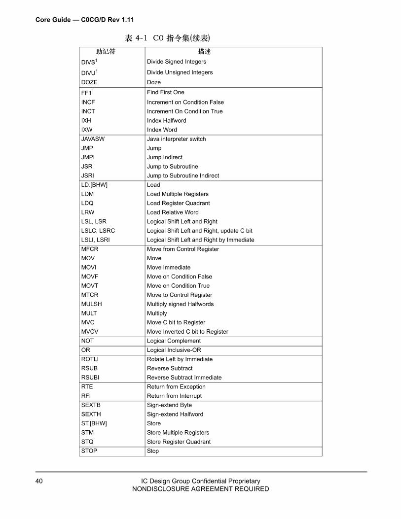
Table 4-1 provides an alphabetized listing of the C0 instruction set.
表4-1 C0指令集 助记符 描述
ABS Absolute ValueADDC Add with C bitADDI Add ImmediateADDU Add UnsignedAND Logical ANDANDI Logical AND ImmediateANDN AND NOTASR Arithmetic Shift RightASRC Arithmetic Shift Right, update C bitASRI Arithmetic Shift Right ImmediateBCLRI Clear Bit BF Branch on Condition FalseBGENI BIt Generate ImmediateBGENR Bit Generate RegisterBKPT BreakpointBMASKI Bit Mask ImmediateBR BranchBREV Bit ReverseBSETI Bit Set ImmediateBSR Branch to SubroutineBT Branch on Condition TrueBTSTI Bit Test ImmediateCLRF Clear Register on Condition FalseCLRT Clear Register on Condition TrueCMPHS Compare Higher or SameCMPLT Compare Less-ThanCMPLTI Compare Less-Than ImmediateCMPNE Compare Not EqualCMPNEI Compare Not Equal ImmediateDECF Decrement on Condition FalseDECGT Decrement Register and Set Condition if Result Greater-than ZeroDECLT Decrement Register and Set Condition if Result Less-than ZeroDECNE Decrement Register and Set Condition if Result Not Equal to ZeroDECT Decrement On Condition True
IC Design Group Confidential ProprietaryNONDISCLOSURE AGREEMENT REQUIRED
39
Core Guide — C0CG/D Rev 1.11
DIVS1 Divide Signed Integers
DIVU1 Divide Unsigned Integers
DOZE Doze
FF11 Find First One
INCF Increment on Condition FalseINCT Increment On Condition TrueIXH Index HalfwordIXW Index WordJAVASW Java interpreter switchJMP JumpJMPI Jump IndirectJSR Jump to SubroutineJSRI Jump to Subroutine IndirectLD.[BHW] LoadLDM Load Multiple RegistersLDQ Load Register QuadrantLRW Load Relative WordLSL, LSR Logical Shift Left and RightLSLC, LSRC Logical Shift Left and Right, update C bitLSLI, LSRI Logical Shift Left and Right by ImmediateMFCR Move from Control RegisterMOV MoveMOVI Move ImmediateMOVF Move on Condition FalseMOVT Move on Condition TrueMTCR Move to Control RegisterMULSH Multiply signed HalfwordsMULT MultiplyMVC Move C bit to RegisterMVCV Move Inverted C bit to RegisterNOT Logical ComplementOR Logical Inclusive-ORROTLI Rotate Left by ImmediateRSUB Reverse SubtractRSUBI Reverse Subtract ImmediateRTE Return from ExceptionRFI Return from InterruptSEXTB Sign-extend ByteSEXTH Sign-extend HalfwordST.[BHW] StoreSTM Store Multiple RegistersSTQ Store Register QuadrantSTOP Stop
表 4-1 C0 指令集(续表)助记符 描述
IC Design Group Confidential ProprietaryNONDISCLOSURE AGREEMENT REQUIRED
40

Core Guide — C0CG/D Rev 1.11
4.7 C0与C300的区别
SUBC Subtract with C bitSUBU SubtractSUBI Subtract ImmediateSYNC SynchronizeTRAP TrapTST Test OperandsTSTNBZ Test for No Byte Equal ZeroWAIT WaitXOR Exclusive ORXSR Extended Shift RightXTRB0 Extract Byte 0XTRB1 Extract Byte 1XTRB2 Extract Byte 2XTRB3 Extract Byte 3ZEXTB Zero-extend ByteZEXTH Zero-extend Halfword
NOTES:1. Not implemented in the current version.
表4-2 C0和C300的比较 指标 C0 C300Pipeline 3 stages 4 stages
Alternative Registers Not available 16
Control Registers
Only a modified PSR; No EPC/EPSR. When enterring/exiting exception /interrupt, processor will automatically push/pop PC and PSR.
12
External Bus AHB-lite CLB
Hardware multiplier A single-cycle or 32-cycles iterative 32-bit x 32-bit multiplier A 32-bit x 16-bit multiplier
Autovectored Interrupt No support SupportEmbedded interrupt
Controller Yes No
DIV/FF1/JAVASW Removed Support
STOP/DOZE/WAIT Executable in both user and supervisor mode Only executable in supervisor mode
Gate Count 12K~20K 45K~ 70K
表 4-1 C0指令集(续表)助记符 描述
IC Design Group Confidential ProprietaryNONDISCLOSURE AGREEMENT REQUIRED
41

Core Guide — C0CG/D Rev 1.11
IC Design Group Confidential ProprietaryNONDISCLOSURE AGREEMENT REQUIRED
42

Core Guide — C0CG/D Rev 1.11
第五节:嵌入式中断控制器
本节介绍了C0处理器的嵌入式中断控制器。
5.1 介绍
中断控制器收集来自各个中断源产生的中断,并提供了一个CPU中断逻辑接口。
5.2 特性
中断控制器的特性如下所示:
• 中断源多达32个,并且可配置
• 每个中断源都有32个独特的可编程优先级
• 根据优先级可独立地启用/禁用中断
• 每个中断源都有一个固定的向量数量
• 支持电平和脉冲触发中断
• Support PendTrap function
• 支持软件复位
IC Design Group Confidential ProprietaryNONDISCLOSURE AGREEMENT REQUIRED
43

Core Guide — C0CG/D Rev 1.11
5.3 内存映射和寄存器
本节描述了内存映射(见表5-1)和寄存器。
5.3.1 内存映射
EIC模块的基本地址(EIC_BASEADDR)是由C0处理器定义的内部变量, 默认值是 0xE0000000. 。EIC寄存器的实际地址是EIC_BASEADDR加上各个EIC寄存器的偏移地址。核心内部模块占用64K的地址范围。系统应避免映射区为EIC_BASEADDR 到 EIC_BASEADDR+0x0000_ffff的寄存器。
表5 - 1中断控制器模块内存映射偏移
地址 位 31-24 位 23-16 位 15-8 位 7-0 访问 (1)
说明:1. 在C0处理器里,任何情况下寄存器都可以被访问。
0x0000_0000 中断状态寄存器(ICSR) S/U0x0000_0004 保留 S/U0x0000_0008 保留 S/U0x0000_000c 保留 S/U0x0000_0010 中断使能寄存器 (IER) S/U0x0000_0014 保留 S/U0x0000_0018 中断设置寄存器 (IPSR) S/U0x0000_001c 中断清除寄存器(IPCR) S/U0x0000_0020
through0x0000_003c
未定义(2)
2. 访问未定义的地址没有影响,导致循环终止传输错误。.
—
优先级选择寄存器 (PLSR0-PLSR31)0x0000_0040 PLSR3 PLSR2 PLSR1 PLSR0 S/U0x0000_0044 PLSR7 PLSR6 PLSR5 PLSR4 S/U0x0000_0048 PLSR11 PLSR10 PLSR9 PLSR8 S/U0x0000_004c PLSR15 PLSR14 PLSR13 PLSR12 S/U0x0000_0050 PLSR19 PLSR18 PLSR17 PLSR16 S/U0x0000_0054 PLSR23 PLSR22 PLSR21 PLSR20 S/U0x0000_0058 PLSR27 PLSR26 PLSR25 PLSR24 S/U0x0000_005c PLSR31 PLSR30 PLSR29 PLSR28 S/U0x0000_0060 系统优先级选择寄存器(SYSPLSR) S/U0x0000_0064
through0x0000_007c
未定义(2) —
IC Design Group Confidential ProprietaryNONDISCLOSURE AGREEMENT REQUIRED
44

Core Guide — C0CG/D Rev 1.11
5.3.2 寄存器
本节包含一个描述中断控制器模块的寄存器。
5.3.2.1 中断控制状态寄存器
32位中断控制寄存器(ICSR)反映了CPU的中断控制器输出状态。
图5 - 1中断控制状态寄存器(ICSR)
SRST — 软件复位位该只读位是用来创建一个软件复位请求的。 设置此位将会在SYSRESETREQ信号上生成一个 脉冲信号。该位始终返回0。
SetPTrap — Set PendTrap BitThe read/write bit is used to create a pending software interrupt. The action is similar to execute “trap” instruction. However the pending software interrupt will not be enterred until all the higher priority exceptions/interrupts exit. When the software interrupt enterred, the bit will be cleared automatically. Reset also clears this bit.On reads :
1 = the software interrupt is pending 0 = the software interrupt is not pending
On writes :1 = set software interrupt to pending0 = no effect
地址 : EIC_BASEADDR+0x0000_0000 31 30 29 28 27 26 25 24
RSRST
0 0SetPTrap ClrPTrap
0 0 0W
RESET: 0 0 0 0 0 0 0 0
23 22 21 20 19 18 17 16R 0 0 0 0 0 0 0 0W
RESET: 0 0 0 0 0 0 0 0
15 14 13 12 11 10 9 8R 0 0 0 0 0 0 0 0W
RESET: 0 0 0 0 0 0 0 0
7 6 5 4 3 2 1 0R 0 VEC6 VEC5 VEC4 VEC3 VEC2 VEC1 VEC0W
RESET: 0 0 0 0 0 0 0 0
= Writes have no effect and the access terminates without a transfer error exception.
IC Design Group Confidential ProprietaryNONDISCLOSURE AGREEMENT REQUIRED
45

Core Guide — C0CG/D Rev 1.11
ClrPTrap — Clear PendTrap BitThe read/write ClrDSI bit is used to cancel the pending software interrupt(PendTrap). Reset clears this bit.On reads :
1 = the software interrupt is pending 0 = the software interrupt is not pending
On writes :1 = cancel the pending software interrupt0 = no effect
VEC[6:0] — 中断向量表该只读VEC[6:0]位包含了7位中断向量号。复位清除VEC[6:0]。
IC Design Group Confidential ProprietaryNONDISCLOSURE AGREEMENT REQUIRED
46

Core Guide — C0CG/D Rev 1.11
的 es
5.3.2.2 中断使能寄存器
Th该可读/写的32位中断使能寄存器(IER)可以单独地使能当前任何等待的中断,并为每个正常中断源分配一个优先级。enabling an interrupt source which has an asserted request causthat request to become pending, and a request to the CPU is asserted if not already outstanding.
图5-2 中断使寄存器(IER)
IE[31:0] — 中断使能位The r该可读/写的IE[31:0]位可以使能在相应的优先级的中断请求源的中断请求。复位清零。
1 = 允许中断请求0 = 禁止中断请求
地址: EIC_BASEADDR+0x0000_001031 30 29 28 27 26 25 24
RIE31 IE30 IE29 IE28 IE27 IE26 IE25 IE24
WRESET: 0 0 0 0 0 0 0 0
23 22 21 20 19 18 17 16R
IE23 IE22 IE21 IE20 IE19 IE18 IE17 IE16W
RESET: 0 0 0 0 0 0 0 0
15 14 13 12 11 10 9 8R
IE15 IE14 IE13 IE12 IE11 IE10 IE9 IE8W
RESET: 0 0 0 0 0 0 0 0
7 6 5 4 3 2 1 0R
IE7 IE6 IE5 IE4 IE3 IE2 IE1 IE0W
RESET: 0 0 0 0 0 0 0 0
= Writes have no effect and the access terminates without a transfer error exception.
IC Design Group Confidential ProprietaryNONDISCLOSURE AGREEMENT REQUIRED
47

Core Guide — C0CG/D Rev 1.11
5.3.2.3 Interrupt Pend Set Register
Figure 5-3 Interrupt Pend Set Register (IPSR)
SetPend[31:0] — Interrupt Pend Set FieldThe read/write SetPend[31:0] field set pend to associated interrupt and indicate whether the associated interrupt is pending . Reset clears SetPend[31:0].On reads :
1 = the associated interrupt is pending 0 = the associated interrupt is not pending
On writes :1 = change the state of associated interrupt to pending0 = no effect
地址: EIC_BASEADDR+0x0000_001831 30 29 28 27 26 25 24
RSetPend31 SetPend30 SetPend29 SetPend28 SetPend27 SetPend26 SetPend25 SetPend24
WRESET: 0 0 0 0 0 0 0 0
23 22 21 20 19 18 17 16R
SetPend23 SetPend22 SetPend21 SetPend20 SetPend19 SetPend18 SetPend17 SetPend16W
RESET: 0 0 0 0 0 0 0 0
15 14 13 12 11 10 9 8R
SetPend15 SetPend14 SetPend13 SetPend12 SetPend11 SetPend10 SetPend9 SetPend8W
RESET: 0 0 0 0 0 0 0 0
7 6 5 4 3 2 1 0R
SetPend7 SetPend6 SetPend5 SetPend4 SetPend3 SetPend2 SetPend1 SetPend0W
RESET: 0 0 0 0 0 0 0 0
= Writes have no effect and the access terminates without a transfer error exception.
IC Design Group Confidential ProprietaryNONDISCLOSURE AGREEMENT REQUIRED
48
Core Guide — C0CG/D Rev 1.11
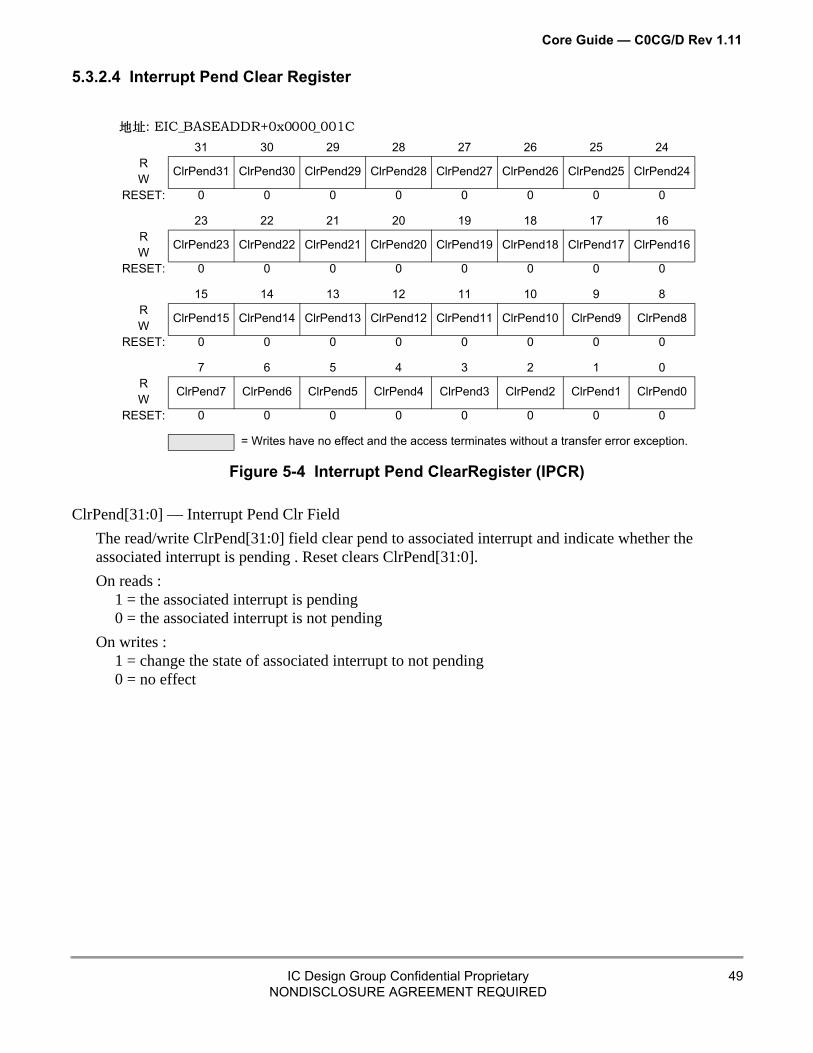
5.3.2.4 Interrupt Pend Clear Register
Figure 5-4 Interrupt Pend ClearRegister (IPCR)
ClrPend[31:0] — Interrupt Pend Clr FieldThe read/write ClrPend[31:0] field clear pend to associated interrupt and indicate whether the associated interrupt is pending . Reset clears ClrPend[31:0].On reads :
1 = the associated interrupt is pending 0 = the associated interrupt is not pending
On writes :1 = change the state of associated interrupt to not pending0 = no effect
地址: EIC_BASEADDR+0x0000_001C31 30 29 28 27 26 25 24
RClrPend31 ClrPend30 ClrPend29 ClrPend28 ClrPend27 ClrPend26 ClrPend25 ClrPend24
WRESET: 0 0 0 0 0 0 0 0
23 22 21 20 19 18 17 16R
ClrPend23 ClrPend22 ClrPend21 ClrPend20 ClrPend19 ClrPend18 ClrPend17 ClrPend16W
RESET: 0 0 0 0 0 0 0 0
15 14 13 12 11 10 9 8R
ClrPend15 ClrPend14 ClrPend13 ClrPend12 ClrPend11 ClrPend10 ClrPend9 ClrPend8W
RESET: 0 0 0 0 0 0 0 0
7 6 5 4 3 2 1 0R
ClrPend7 ClrPend6 ClrPend5 ClrPend4 ClrPend3 ClrPend2 ClrPend1 ClrPend0W
RESET: 0 0 0 0 0 0 0 0
= Writes have no effect and the access terminates without a transfer error exception.
IC Design Group Confidential ProprietaryNONDISCLOSURE AGREEMENT REQUIRED
49

Core Guide — C0CG/D Rev 1.11
5.3.2.5 优先级选择寄存器
The read/write 8-bit Priority Level Select Registers (PLSRx) are 32 read/write, 8-bit priority level select registers PLSR0–PLSR31, one for each of the interrupt source. The PLSRx register assigns a priority level to interrupt source x.
Figure 5-5 Priority Level Select Registers (PLSR0-PLSR31)
PLSRx[7:6] — Priority Level Select FieldIRQ0~31 has a default priority value 0~31. The lower the value, the higher the priority. That means IRQ0 priority > IRQ1 > ... > IRQ31 as default. However, user can set PLSRx[7:6] to adjust the interrupt priority. The actual value of priority level is the default value plus PLSRx[7:6] *64. For instance, if PLSR1[7:6] = 2, IRQ1’s priority value is 1+2*64 = 129, then IRQ1’s priority is lower than any IRQ with lower priority value.
Address : EIC_BASEADDR+0x0000_0040 through EIC_BASEADDR+0x0000_005c7 6 5 4 3 2 1 0
RPLSR[7] PLSR[6]
0 0 0 0 0 0W
RESET: 0 0 0 0 0 0 0 0
= Writes have no effect and the access terminates without a transfer error exception.
Table 5-2 Priority Value AdjustmentPLSRx[7:6] Plused Priority Value
00 0 01 6410 12811 192
IC Design Group Confidential ProprietaryNONDISCLOSURE AGREEMENT REQUIRED
50

Core Guide — C0CG/D Rev 1.11
5.3.2.6 系统优先级选择寄存器
图5-6 系统优先级选择寄存器 (SYSPLSR)
EPTPRI[7:6] — EPT 优先级选择位EPT 中断的默认优先级是-2,这意味着EPT中断的优先级比其他正常的中断请求和默认的软件中断的优先级都要高。值越低,优先级越高。当然,用户可以通过设置PRI[7:6]位的值来调整EPT中断的优先级。EPT中断优先级的实际值等于默认值加上PRI[7:6]*64。举例说明,如果PRI[7:6]=2,那么EPT中断优先级的值就为-2+2*64 = 126。
SIPRI[7:6] — 软件中断优先级选择位软件中断默认的优先级是-1。这意味着EPT中断优先级比其他中断请求的优先级都要高。值越低,优先级越高。当然,用户可以设置SIPRI [ 7:6 ]调整软件中断优先级。优先级的实际值等 于默认值加上SIPRI [ 7:6 ]×64。例如,如果SIPRI[7:6]=2,那么软件中断的优先级值是 -1 + 2 * 64 = 127。 地址
地址: EIC_BASEADDR+0x0000_006031 30 29 28 27 26 25 24
REPTPRI[7] EPTPRI[6]
0 0 0 0 0 0W
RESET: 0 0 0 0 0 0 0 0
23 22 21 20 19 18 17 16R
SIPRI[7] SIPRI[6]0 0 0 0 0 0
WRESET: 0 0 0 0 0 0 0 0
15 14 13 12 11 10 9 8R 0 0 0 0 0 0 0 0W
RESET: 0 0 0 0 0 0 0 0
7 6 5 4 3 2 1 0R 0 0 0 0 0 0 0 0W 0 0
RESET: 0 0 0 0 0 0 0 0
= Writes have no effect and the access terminates without a transfer error exception.
表 5-3 优先级调整值PRI[7:6] 加上优先级值
00 0 01 6410 12811 192
IC Design Group Confidential ProprietaryNONDISCLOSURE AGREEMENT REQUIRED
51

Core Guide — C0CG/D Rev 1.11
表 5-4 优先级调整值PRI[7:6] 加上优先级值
00 0 01 6410 12811 192
IC Design Group Confidential ProprietaryNONDISCLOSURE AGREEMENT REQUIRED
52

Core Guide — C0CG/D Rev 1.11
5.4 功能描述
EIC 同时支持水平敏感和脉冲中断。中断源的数量从1到32。
中断未决是由以下原因之一造成的:
• EIC检测到中断信号是有效的,但对应的中断没有激活
• EIC在中断信号中检测到一个上升沿
等待处理的中断仍然等待直到以下情况之一:
• 处理器进入了中断的中断服务程序,这使得中断从等待状态进入激活状态。
– For a level-sensitive interrupt, when the processor returns from the ISR, the EIC samples the interrupt signal. If the signal is asserted, the state of the interrupt changes to pending, which might cause the processor to immediately re-enter the ISR. Otherwise, the state of the interrupt changes to inactive.
– For a pulse interrupt, the EIC continues to monitor the interrupt signal,and if this is pulsed the state of the interrupt changes to pending and active.In this case, when the processor returns from the ISR the state of the interrupt changes to pending, which might cause the processor to immediately re-enter the ISR.If the interrupt signal is not pulsed while the processor is in the ISR, when the processor returns from the ISR the state of the interrupt changes to inactive.
• Software writes to the corresponding interrupt Pend Clear Register bit.
5.4.1 无冲突的中断处理
If an interrupt is pulsed, the state of the interrupt changes to pending. Without confliction, the interrupt causes the processor to immediately enter the ISR. When the processor returns from the ISR, the state of the interrupt changes to inactive.
Figure 5-7 One Pulse Interrupt without confliction
ISR start ISR end
PC when IRQ occurs
PC when IRQ occurs
PSRwhen IRQ occurs
PSRwhen IRQ occurs
IRQx
ISR
PC
PSR
IC Design Group Confidential ProprietaryNONDISCLOSURE AGREEMENT REQUIRED
53

Core Guide — C0CG/D Rev 1.11
For a level-sensitive interrupt, the state of the interrupt changes to pending if the signal is asserted. Without confliction, the interrupt causes the processor to immediately enter the ISR. When the processor returns from the ISR, EIC continues to samples the interrupt signal. If the signal is not cleared, the processor will re-enter the ISR. Otherwise, the state of the interrupt changes to inactive.
图5-8 无冲突的电平中断
ISR start ISR endISR startISR endIRQ
ISR
IC Design Group Confidential ProprietaryNONDISCLOSURE AGREEMENT REQUIRED
54

Core Guide — C0CG/D Rev 1.11
5.4.2 中断冲突
When two interrupt signals are asserted at the same time , the Interrupt Arbiter will judge which one has the greater priority. For instance, if the priority of IRQx is greater than IRQy , the processor will enter ISRx and IRQy becomes pending. After the processor returns from ISRx, the processor will enter ISRy immediately.
图5-9 两个中断同时发生
如果一个中断在另一个中断处理过程中生效,那么有两种可能:
1. 已经生效了的中断的优先级低于正在处理的中断,如果是这样的话,那么已经生效的中断处于等待状态,直到正在处理的中断结束。
2. 已经生效了的中断的优先级高于正在处理的中断,如果是这样的话,那么已经生效的中断 将嵌套在低优先级的中断里。
图 5-10 有冲突的低优先级中断
ISRx start ISRy endISRy startISRx end
IRQx
IRQy
ISR
ISRx start ISRx end ISRy start ISRy end
IRQx
IRQy
ISR
IC Design Group Confidential ProprietaryNONDISCLOSURE AGREEMENT REQUIRED
55

Core Guide — C0CG/D Rev 1.11
图 5-11 有冲突的高优先级中断
5.4.3 Pend Trap function
SetPTrap/ClrPTrap bits in ICSR are used to create/cancel a “pending” software interrupt request while a higher priority interrupt is handling .As soon as the processor returns from the higher priority interrupt , the “pending” software interrupt will be accepted by the processor.
Usually, Pend Trap function is used for OS task passive switch .
5.5 Interrupus
中断控制器为每个中断源都分配一个编号。如图5-5所示。
表5-5 中断源分配 源 模块 标志 中断源描述 标志清除机制
0 ADC
1 SPI
MODF 模式错误EOTF 发送完成 Write-One Clear
TXFTO TXFIFO 超时 Write-One ClearTXFOVF TXFIFO 上溢 Write-One ClearTXFUDF TXFIFO 下溢 Write-One ClearTXFSER TXFIFO 服务 Write-One ClearRXFTO RXFIFO 超时 Write-One Clear
RXFOVF RXFIFO 上溢 Write-One ClearRXFUDF RXFIFO 下溢 Write-One ClearRXFSER RXFIFO 服务 Write-One Clear
2 SCI0
TDRE/TFTSTC/FTC
RDRF/RFTSOR/FOR
IDLERTOS
ISRx start ISRx endISRy start ISRy end
IRQx
IRQy
ISR
IC Design Group Confidential ProprietaryNONDISCLOSURE AGREEMENT REQUIRED
56

Core Guide — C0CG/D Rev 1.11
3 SCI1
TDRE/TFTSTC/FTC
RDRF/RFTSOR/FOR
IDLERTOS
4 Reserved
5 LDMAC
DONE[0] Write DONE[0]=1
DONE[1] Write DONE[1]=1
DONE[2] Write DONE[2]=1
DONE[3] Write DONE[3]=1
6 WDT IF
7 PWM0
PIFR[0]PIFR[1]PIFR[2]PIFR[3]
8 PWM1
PIFR[0]PIFR[1]PIFR[2]PIFR[3]
9 PIT0 PIF PIT Flag Writing a 1 to it or writing to PMR
10 PIT1 PIF PIT Flag Writing a 1 to it or writing to PMR
11 PIT2 PIF PIT Flag Writing a 1 to it or writing to PMR
12 PIT3 PIF PIT Flag Writing a 1 to it or writing to PMR
13 PIT4 PIF PIT Flag Writing a 1 to it or writing to PMR
14 EFM PVDO PVD Flag15 I2C I2C Flag I2C Flag16 EPORT0 EPF0 Edge port 0 flag 0 Write EPF0 = 1
17 EPORT0 EPF1 Edge port 0 flag 1 Write EPF1 = 1
18 EPORT0 EPF2 Edge port 0 flag 2 Write EPF2 = 1
19 EPORT0 EPF3 Edge port 0 flag 3 Write EPF3 = 1
20 EPORT0 EPF4 Edge port 0 flag 4 Write EPF4 = 1
21 EPORT0 EPF5 Edge port 0 flag 5 Write EPF5 = 1
22 EPORT0 EPF6 Edge port 0 flag 6 Write EPF6 = 1
23 EPORT0 EPF7 Edge port 0 flag 7 Write EPF7 = 1
24 EPORT1 EPF0 Edge port 0 flag 0 Write EPF0 = 1
25 EPORT1 EPF1 Edge port 0 flag 1 Write EPF1 = 1
26 EPORT1 EPF2 Edge port 0 flag 2 Write EPF2 = 1
27 EPORT1 EPF3 Edge port 0 flag 3 Write EPF3 = 1
28 EPORT1 EPF4 Edge port 0 flag 4 Write EPF4 = 1
29 EPORT1 EPF5 Edge port 0 flag 5 Write EPF5 = 1
表5-5 中断源分配 源 模块 标志 中断源描述 标志清除机制
IC Design Group Confidential ProprietaryNONDISCLOSURE AGREEMENT REQUIRED
57

Core Guide — C0CG/D Rev 1.11
30 EPORT1 EPF6 Edge port 0 flag 6 Write EPF6 = 1
31 Reserved
表5-5 中断源分配 源 模块 标志 中断源描述 标志清除机制
IC Design Group Confidential ProprietaryNONDISCLOSURE AGREEMENT REQUIRED
58

Core Guide — C0CG/D Rev 1.11
第六节:可编程的嵌入式定时器
6.1 说明
可编程的嵌入式定时器(EPT)是一个24位的定时器,它提供了精确的,处理器最小干预的定期中断。定时器可以从重载值中计数,也可以是一个自由运行计数器。
EPT的中断可以触发一个异常(向量数= 24)。
EPT 模块通过设置“EPT”参数为0来移除,从而可以降低处理器的门数。
6.2 内存映射和寄存器
6.2.1 内存映射
EPT 的基地址被定义为EIC_BASEADDR +0x1000。默认的基地址0xe0001000。表6-1 列出了EPT寄存器的偏移地址。EPT模块占用4K的地址区。
表 6-1 可编程定时器的内存映射偏移
地址 位31-24 位 23-16 位 15-8 位7-0 访问 (1)
说明:1. 在C0处理器中,任何情况下寄存器都可以被访问。
0x0000_0000 EPT 控制与状态寄存器 (EPTCSR) S/U0x0000_0004 EPT 重载寄存器 (EPTRLD) S/U0x0000_0008 EPT 计数寄存器 (EPTCNT) S/U0x0000_000c 保留 S/U
IC Design Group Confidential ProprietaryNONDISCLOSURE AGREEMENT REQUIRED
59

Core Guide — C0CG/D Rev 1.11
6.2.2 寄存器
本节包含EPT模块寄存器的描述。
6.2.2.1 EPT 控制状态寄存器
图 6-1 EPT 控制状态寄存器 (EPTCSR)
CNTFLAG — 计数到0的标志该只读位指示了定时器计数到0的情况。该位被HRESETn复位
1 = 定时器已经计数到0.0 = 定时器仍在计数.
CLKSRC — 计数时钟源选择该位负责计数时钟源的选择。该位被HRESETn复位。
1 = 内部时钟.0 = 外部参考时钟
INTEN — EPT 中断请求使能当定时器计数到0时,该位负责使能EPT的中断。该位被RESET复位。
1 = 当定时器计数到0时,EPT产生异常请求。0 = 当定时器计数到0时,EPT不产生异常请求。
地址 : EPT_BASEADDR+0x0000_0000 31 30 29 28 27 26 25 24
R 0 0 0 0 0 0 0 0W
RESET: 0 0 0 0 0 0 0 0
23 22 21 20 19 18 17 16R 0 0 0 0 0 0 0 CNTFLAGW
RESET: 0 0 0 0 0 0 0 0
15 14 13 12 11 10 9 8R 0 0 0 0 0 0 0 0W
RESET: 0 0 0 0 0 0 0 0
7 6 5 4 3 2 1 0R 0 0 0 0 0 CLKSRC INTEN CNTENW
RESET: 0 0 0 0 0 0 0 0
= Writes have no effect and the access terminates without a transfer error exception.
IC Design Group Confidential ProprietaryNONDISCLOSURE AGREEMENT REQUIRED
60

Core Guide — C0CG/D Rev 1.11
CNTEN — 计数器使能该可读/写位是用来使能EPT计数器的。该位被RESET复位。
1 = 计数器使能0 = 计数器禁止
IC Design Group Confidential ProprietaryNONDISCLOSURE AGREEMENT REQUIRED
61

Core Guide — C0CG/D Rev 1.11
6.2.2.2 EPT 重载寄存器
图 6-2 EPT 重载寄存器 (EPTRLD)
RLD[23:0] — 重装值该可读/写的RLD[23:0]指定了当定时器计数到0时的重载值。 寄存器没有复位值。RLD值的范围为0x00000001 ~ 0x00FFFFFF之间的任何值,但如果RLD的值为0时也不会产生坏影响。如果要产生一个N时钟循环的周期定时器,那么需要设置RLD的值为N-1。
地址 : EPT_BASEADDR+0x0000_000431 30 29 28 27 26 25 24
R 0 0 0 0 0 0 0 0W
RESET: x x x x x x x x
23 22 21 20 19 18 17 16R
RLD[23] RLD[22] RLD[21] RLD[20] RLD[19] RLD[18] RLD[17] RLD[16]W
RESET: x x x x x x x x
15 14 13 12 11 10 9 8R
RLD[15] RLD[14] RLD[13] RLD[12] RLD[11] RLD[10] RLD[9] RLD[8]W
RESET: x x x x x x x x
7 6 5 4 3 2 1 0R
RLD[7] RLD[6] RLD[5] RLD[4] RLD[3] RLD[2] RLD[1] RLD[0]W
RESET: x x x x x x x x
= Writes have no effect and the access terminates without a transfer error exception.
IC Design Group Confidential ProprietaryNONDISCLOSURE AGREEMENT REQUIRED
62

Core Guide — C0CG/D Rev 1.11
6.2.2.3 EPT计数寄存器
图 6-3 EPT 计数寄存器 (EPTCNT)
CNT[23:0] — EPT 的计数值 该只读寄存器表明了EPT定时器的当前计数值。该寄存器没有复位值。读该寄存器会返回EPT定时器的当前值。不管向该寄存器写入任何值,都会将计数值置0,并且将CNTFLAG清零。 .
地址 : EPT_BASEADDR+0x0000_000831 30 29 28 27 26 25 24
R 0 0 0 0 0 0 0 0W
RESET: x x x x x x x x
23 22 21 20 19 18 17 16R CNT[23] CNT[22] CNT[21] CNT[20] CNT[19] CNT[18] CNT[17] CNT[16]W
RESET: x x x x x x x x
15 14 13 12 11 10 9 8R CNT[15] CNT[14] CNT[13] CNT[12] CNT[11] CNT[10] CNT[9] CNT[8]W
RESET: x x x x x x x x
7 6 5 4 3 2 1 0R CNT[7] CNT[6] CNT[5] CNT[4] CNT[3] CNT[2] CNT[1] CNT[0]W
RESET: x x x x x x x x
= Writes have no effect and the access terminates without a transfer error exception.
IC Design Group Confidential ProprietaryNONDISCLOSURE AGREEMENT REQUIRED
63

Core Guide — C0CG/D Rev 1.11
IC Design Group Confidential ProprietaryNONDISCLOSURE AGREEMENT REQUIRED
64

Core Guide — C0CG/D Rev 1.11
6.3 功能描述
当启用时,EPT将从设定好的RLD的值倒数至0,然后在下一个周期循环里将值重装到RLD,接着继续倒数。往RLD里写入0会禁止计数器的下一次倒数。当计数器倒数到0时,CLFAG会被置为1,并且如果INTEN使能的话,EPT将会触发EPT中断。 .
读CSR会将CFLAG位清零,往CNT里写入任何值同样会将CFLAG清零。
6.3.1 计数时序
图6-4 EPT计数显示
1 2 3 4 5 6 7 8 9 10 11 12 13 14 15
0x5
0x4 0x3 0x2 0x1 0x00x5 0x4 0x3 0x2 0x1 0x00x50x0
Write any value to CNT to clear cflag set by counted to zero
cflag clear by read CSR
CNT auto reload with RLD
Clock
CNT
RLD
PITEN
CFLAG
EPT intreq
IC Design Group Confidential ProprietaryNONDISCLOSURE AGREEMENT REQUIRED
65

Core Guide — C0CG/D Rev 1.11
IC Design Group Confidential ProprietaryNONDISCLOSURE AGREEMENT REQUIRED
66

Chip Configuration Module (CCM) Introduction
第七节:芯片配置模块(CCM)
7.1 说明
芯片配置模块(CCM)控制着芯片的配置。
7.2 特性
CCM执行如下操作:
• 配置唤醒功能
• 配置LDO模式
• 配置I/O口功能
LT32A01 IC Design Group Confidential Proprietary
NON-DISCLOSURE AGREEMENT REQUIRED 67

Chip Configuration Module (CCM) Memory Map and Registers
7.3 内存映射和寄存器
本小节描述了内存映射和寄存器。
7.3.1 内存映射
表 7-1 CC M 的内存映射
偏移 地址 31:16 15:0 访问1
0x0000 WKUPC — 唤醒配置寄存器 S0x0004 CRPDC — 芯片降低引脚驱动配置寄存器 S0x0008 CPSRC — 芯片管脚减速配置寄存器 S0x000c CPPDC — 芯片引脚下拉配置寄存器 S0x0010 CIR — 芯片识别寄存器 CTR — 芯片测试寄存器 S
说明:
1. S = 只有管理员才能访问。如果在用户模式下访问管理员地址时,会造成周期终止传输错误。
LT32A01 IC Design Group Confidential Proprietary
NON-DISCLOSURE AGREEMENT REQUIRED 68

Chip Configuration Module (CCM) Memory Map and Registers
7.3.2 寄存器描述
7.3.2.1 WKUPC —唤醒配置寄存器
图 7-1 WKUPC — 唤醒配置寄存器
WKUPFILTEREN— 唤醒源滤波器使能如果WKUPFILTEREN 位被设置了,那么唤醒源会通过一个滤波器去除毛刺并 唤醒芯片的待机模式。
1 = 唤醒源滤波器使能0 = 唤醒源滤波器禁止
WKUPSEN— 唤醒源使能该位控制是否有相应的源用来源唤醒芯片的待机模式。如果设置,相应的源作为 唤醒源。
表 7-2 列出了 WKUPSEN 和与其相应的唤醒源。
Address : 0x0000 31 30 29 28 27 26 25 24
R WKUPFIL-TEREN
0 0 0 0 0 0 0W
RESET: 0 0 0 0 0 0 0 0
23 22 21 20 19 18 17 16R 0 0 0
WKUPSEN[20:16]W
RESET: 0 0 0 1 1 1 1 1
15 14 13 12 11 10 9 8R
WKUPSEN[15:8]W
RESET: 1 1 1 1 1 1 1 1
7 6 5 4 3 2 1 0R
WKUPSEN[7:0]W
RESET: 1 1 1 1 1 1 1 1
= Writes have no effect and the access terminates without a transfer error exception.
LT32A01 IC Design Group Confidential Proprietary
NON-DISCLOSURE AGREEMENT REQUIRED 69

Chip Configuration Module (CCM) Memory Map and Registers
表 7-2 WKUPSEN 和与其相应的唤醒源WKUPSEN 唤醒源
WKUPSEN[20] i2cWKUPSEN[19] WDT 中断WKUPSEN[18] JTAG上电请求WKUPSEN[17] resetb 引脚WKUPSEN[16] WDT 复位WKUPSEN[15] int1[7]WKUPSEN[14] int1[6]WKUPSEN[13] int1[5]WKUPSEN[12] int1[4]WKUPSEN[11] int1[3]WKUPSEN[10] int1[2]WKUPSEN[9] int1[1]WKUPSEN[8] int1[0]WKUPSEN[7] int0[7]WKUPSEN[6] int0[6]WKUPSEN[5] int0[5]WKUPSEN[4] int0[4]WKUPSEN[3] int0[3]WKUPSEN[2] int0[2]WKUPSEN[1] int0[1]WKUPSEN[0] int0[0]
LT32A01 IC Design Group Confidential Proprietary
NON-DISCLOSURE AGREEMENT REQUIRED 70

Chip Configuration Module (CCM) Memory Map and Registers
7.3.2.2 CRPDC — 芯片降低引脚驱动配置寄存器
图 7-2 CPSC — 芯片降低引脚驱动配置寄存器
RPD — 降低引脚驱动位该可读/写位控制了相应引脚的驱动能力,如表7-3所示。
1 = 降低引脚驱动0 = 不降低引脚驱动
地址 : 0x0004 31 30 29 28 27 26 25 24
RRPD[31:24]
WRESET: 1 1 1 1 1 1 1 1
23 22 21 20 19 18 17 16R
RPD[23:16]W
RESET: 1 1 1 1 1 1 1 1
15 14 13 12 11 10 9 8R
RPD[15:8]W
RESET: 1 1 1 1 1 1 1 1
7 6 5 4 3 2 1 0R
RPD[7:0]W
RESET: 1 1 1 1 1 1 1 1
= Writes have no effect and the access terminates without a transfer error exception.
表7-3 芯片降低引脚驱动配置
管脚名 驱动力配置位 引脚的驱动能力
ss, sck, miso,mosi. RPD[31] 1: 6mA0:12mA
rxd0,txd0 RPD[30] 1: 6mA0:12mA
rxd1,txd1 RPD[29] 1: 6mA0:12mA
scl,sda RPD[28] 1: 6mA0:12mA
LT32A01 IC Design Group Confidential Proprietary
NON-DISCLOSURE AGREEMENT REQUIRED 71

Chip Configuration Module (CCM) Memory Map and Registers
pwm0[3] RPD[27] 0: 24mA1:12mA
pwm0[2] RPD[26] 0: 24mA1:12mA
pwm0[1] RPD[25] 0: 24mA1:12mA
pwm0[0] RPD[24] 0: 24mA1:12mA
pwm1[3] RPD[23] 0: 24mA1:12mA
pwm1[2] RPD[22] 0: 24mA1:12mA
pwm1[1] RPD[21] 0: 24mA1:12mA
pwm1[0] RPD[20] 0: 24mA1:12mA
Reversed RPD[19]Reversed RPD[18]Reversed RPD[17]Reversed RPD[16]
ain[7] RPD[15] 1: 6mA0:12mA
ain[6] RPD[14] 1: 6mA0:12mA
ain[5] RPD[13] 1: 6mA0:12mA
ain[4] RPD[12] 1: 6mA0:12mA
ain[3] RPD[11] 1: 6mA0:12mA
extal RPD[10] 1: 6mA0:12mA
int0[1] RPD[9] 1: 6mA0:12mA
int0[0] RPD[8] 1: 6mA0:12mA
xtal RPD[7] 1: 6mA0:12mA
rstout RPD[6] 1: 6mA0:12mA
表7-3 芯片降低引脚驱动配置
管脚名 驱动力配置位
引脚驱动能力
LT32A01 IC Design Group Confidential Proprietary
NON-DISCLOSURE AGREEMENT REQUIRED 72

Chip Configuration Module (CCM) Memory Map and Registers
7.3.2.3 CPSRC — 芯片引脚降速配置寄存器
图 7-3 CPSRC — 芯片引脚降速配置寄存器
PSRC — 引脚降速配置位
int1[5] RPD[5] 1: 6mA0:12mA
int1[4] RPD[4] 1: 6mA0:12mA
int1[3] RPD[3] 1: 6mA0:12mA
int1[2] RPD[2] 1: 6mA0:12mA
int1[1] RPD[1] 1: 6mA0:12mA
clkout RPD[0] 1: 6mA0:12mA
表7-3 芯片降低引脚驱动配置
管脚名 驱动力配置位
引脚驱动能力
地址 : 0x0008 31 30 29 28 27 26 25 24
RPSRC[31:24]
WRESET: 0 0 0 0 0 0 0 0
23 22 21 20 19 18 17 16R
PSRC[23:16]W
RESET: 0 0 0 0 0 0 0 0
15 14 13 12 11 10 9 8R
PSRC[15:8]W
RESET: 0 0 0 0 0 0 0 0
7 6 5 4 3 2 1 0R
PSRC[7:0]W
RESET: 0 0 0 0 0 0 0 0
= Writes have no effect and the access terminates without a transfer error exception.
LT32A01 IC Design Group Confidential Proprietary
NON-DISCLOSURE AGREEMENT REQUIRED 73

Chip Configuration Module (CCM) Memory Map and Registers
该可读/写位控制相应引脚的速度,如表7-4所示。1 = 芯片速度被限制0 = 芯片速度正常
表 7-4 芯片引脚降速配置
管脚名 降速配置位 速度
ss, sck, miso,mosi PSRC[31] 0: Normal1:Limited
rxd0,txd0 PSRC[30] 0: Normal1:Limited
rxd1,txd1 PSRC[29] 0: Normal1:Limited
scl,sda PSRC[28] 0: Normal1:Limited
pwm0[3] PSRC[27] 0: Normal1:Limited
pwm0[2] PSRC[26] 0: Normal1:Limited
pwm0[1] PSRC[25] 0: Normal1:Limited
pwm0[0] PSRC[24] 0: Normal1:Limited
pwm1[3] PSRC[23] 0: Normal1:Limited
pwm1[2] PSRC[22] 0: Normal1:Limited
pwm1[1] PSRC[21] 0: Normal1:Limited
pwm1[0] PSRC[20] 0: Normal1:Limited
Reversed PSRC[19] 0: Normal1:Limited
Reversed PSRC[18] 0: Normal1:Limited
Reversed PSRC[17] 0: Normal1:Limited
Reversed PSRC[16] 0: Normal1:Limited
ain[7] PSRC[15] 0: Normal1:Limited
ain[6] PSRC[14] 0: Normal1:Limited
LT32A01 IC Design Group Confidential Proprietary
NON-DISCLOSURE AGREEMENT REQUIRED 74

Chip Configuration Module (CCM) Memory Map and Registers
ain[5] PSRC[13] 0: Normal1:Limited
ain[4] PSRC[12] 0: Normal1:Limited
ain[3] PSRC[11] 0: Normal1:Limited
extal PSRC[10] 0: Normal1:Limited
int0[1] PSRC[9] 0: Normal1:Limited
int0[0] PSRC[8] 0: Normal1:Limited
xtal PSRC[7] 0: Normal1:Limited
rstout PSRC[6] 0: Normal1:Limited
int1[5] PSRC[5] 0: Normal1:Limited
int1[4] PSRC[4] 0: Normal1:Limited
int1[3] PSRC[3] 0: Normal1:Limited
int1[2] PSRC[2] 0: Normal1:Limited
int1[1] PSRC[1] 0: Normal1:Limited
clkout PSRC[0] 0: Normal1:Limited
表7-4 芯片引脚降速配置
管脚名 降速配置位 速度
LT32A01 IC Design Group Confidential Proprietary
NON-DISCLOSURE AGREEMENT REQUIRED 75

Chip Configuration Module (CCM) Memory Map and Registers
7.3.2.4 CPPDC — 芯片引脚下拉配置寄存器
图 7-4 CPPDC — 芯片引脚下拉配置寄存器
PPDC — 芯片引脚下拉配置位T该可读/写位控制着相应引脚的下拉功能,如表7-5所示。
1 = 相应引脚的下拉功能使能0 = 相应引脚的下拉功能禁止
地址 : 0x000c31 30 29 28 27 26 25 24
RPPDC[31:24]
WRESET: 0 0 0 0 0 0 0 0
23 22 21 20 19 18 17 16R
PPDC[23:16]W
RESET: 0 0 0 0 0 0 0 0
15 14 13 12 11 10 9 8R
PPDC[15:8]W
RESET: 0 0 0 0 0 0 0 0
7 6 5 4 3 2 1 0R
PPDC[7:0]W
RESET: 0 0 0 0 0 0 0 0
= Writes have no effect and the access terminates without a transfer error exception.
表 7-5 芯片引脚下拉配置
管脚名 下拉配置位 下拉功能
ss, sck, miso,mosi PPDC[31] 0: Disable1:Enable
rxd0,txd0 PPDC[30] 0: Disable1:Enable
rxd1,txd1 PPDC[29] 0: Disable1:Enable
Reversed PPDC[28] 0: Disable1:Enable
LT32A01 IC Design Group Confidential Proprietary
NON-DISCLOSURE AGREEMENT REQUIRED 76

Chip Configuration Module (CCM) Memory Map and Registers
pwm0[3] PPDC[27] 0: Disable1:Enable
pwm0[2] PPDC[26] 0: Disable1:Enable
pwm0[1] PPDC[25] 0: Disable1:Enable
pwm0[0] PPDC[24] 0: Disable1:Enable
pwm1[3] PPDC[23] 0: Disable1:Enable
pwm1[2] PPDC[22] 0: Disable1:Enable
pwm1[1] PPDC[21] 0: Disable1:Enable
pwm1[0] PPDC[20] 0: Disable1:Enable
Reversed PPDC[19] 0: Disable1:Enable
Reversed PPDC[18] 0: Disable1:Enable
Reversed PPDC[17] 0: Disable1:Enable
Reversed PPDC[16] 0: Disable1:Enable
ain[7] PPDC[15] 0: Disable1:Enable
ain[6] PPDC[14] 0: Disable1:Enable
ain[5] PPDC[13] 0: Disable1:Enable
ain[4] PPDC[12] 0: Disable1:Enable
ain[3] PPDC[11] 0: Disable1:Enable
extal PPDC[10] 0: Disable1:Enable
int0[1] PPDC[9] 0: Disable1:Enable
int0[0] PPDC[8] 0: Disable1:Enable
xtal PPDC[7] 0: Disable1:Enable
表 7-5 芯片引脚下拉配置
管脚名 下拉配置位
下拉功能
LT32A01 IC Design Group Confidential Proprietary
NON-DISCLOSURE AGREEMENT REQUIRED 77
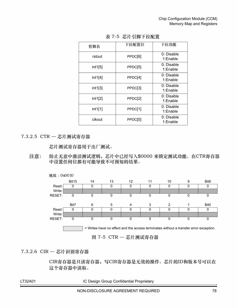
Chip Configuration Module (CCM) Memory Map and Registers
7.3.2.5 CTR — 芯片测试寄存器
芯片测试寄存器用于出厂测试。
注意: 防止无意中激活测试逻辑,芯片中已经写入$0000 来锁定测试功能。在CTR寄存器 中设置任何位都有可能导致不可预知的结果。
图 7-5 CTR — 芯片测试寄存器
7.3.2.6 CIR — 芯片识别寄存器
CIR寄存器是只读寄存器,写CIR寄存器是无效的操作。芯片的ID和版本号可以在这个寄存器中读取。
rstout PPDC[6] 0: Disable1:Enable
int1[5] PPDC[5] 0: Disable1:Enable
int1[4] PPDC[4] 0: Disable1:Enable
int1[3] PPDC[3] 0: Disable1:Enable
int1[2] PPDC[2] 0: Disable1:Enable
int1[1] PPDC[1] 0: Disable1:Enable
clkout PPDC[0] 0: Disable1:Enable
表 7-5 芯片引脚下拉配置
管脚名 下拉配置位
下拉功能
地址 : 0x0010Bit15 14 13 12 11 10 9 Bit8
Read: 0 0 0 0 0 0 0 0Write:
RESET: 0 0 0 0 0 0 0 0
Bit7 6 5 4 3 2 1 Bit0Read: 0 0 0 0 0 0 0 0Write:
RESET: 0 0 0 0 0 0 0 0
= Writes have no effect and the access terminates without a transfer error exception.
LT32A01 IC Design Group Confidential Proprietary
NON-DISCLOSURE AGREEMENT REQUIRED 78

Chip Configuration Module (CCM) Memory Map and Registers
图 7-6 CIR — 芯片识别寄存器
PIN[7:0] — 芯片ID位此只读位包含一个唯一的芯片ID。
PRN[7:0] — 芯片版本号位此只读位包含了芯片的版本号。版本号码是按时间顺序安排。
地址 : 0x001231 30 29 28 27 26 25 24
Read: PINWrite:
RESET: 0 0 1 1 0 0 1 0
23 22 21 20 19 18 17 16Read: PRNWrite:
RESET: 0 0 0 0 0 0 0 1
= Writes have no effect and the access terminates without a transfer error exception.
LT32A01 IC Design Group Confidential Proprietary
NON-DISCLOSURE AGREEMENT REQUIRED 79

Clock and Power Control Module Overview
第八节:时钟和电源控制模块
8.1 概述
时钟模块包括了:
• 内部高速的48MHz振荡器
• 外部晶振/谐振器(12MHz)
• 状态和控制寄存器
• 时钟和电源控制逻辑
8.2 特性
时钟模块的特性包括:
• 2个系统时钟源
– 系统时钟的内部高速48MHz振荡器
– 外部12MHz晶振/谐振器
• IPS,系统和ADC时钟都有独立的时钟分频器
• 支持低功耗模式
• 通过设置MSCR,模块可以单独停止运行
LT32A01 IC Design Group Confidential Proprietary
NON-DISCLOSURE AGREEMENT REQUIRED 80

Clock and Power Control Module Clock Structure
8.3 时钟结构
8.4 时钟源选择
系统的时钟源可以是内部高速48MHz振荡器或者是外部12MHz晶振/谐振器。时钟源的选择是根据选项字节模块的CCR寄存器中的CLKMD位选择的。如果设置了,那么内部高速48MHz振荡器就为系统的时钟源,否则,系统的时钟源是外部12MHz晶振/谐振器。
01
CNT
Oscillator Buffer
I28KHZ Oscillator
Internal Oscillator
CNT
FLL
CNT
0
1
SYSDIV
IPSDIV
ADC_CLK IPG_CLK HCLK SCLK FCLKDCLK
ADCDIV
LT32A01 IC Design Group Confidential Proprietary
NON-DISCLOSURE AGREEMENT REQUIRED 81
Clock and Power Control Module Clock Source Select
8.4.1 低功耗选项
8.4.1.1 等待和休眠模式
在等待和打盹模式中,外设和嵌入式FLASH(EFLASH)的系统时钟是使能的。而CPU,ROM,SRAM的时钟是停止的。每个模块都可以通过局部的模块设置或者设置MSCR来禁止模块时钟。
8.4.1.2 停机模式
在停机模式中,所有的系统时钟都是禁止的。
注意: 在停机模式时,不要往EFLASH编程或者擦除。
LT32A01 IC Design Group Confidential Proprietary
NON-DISCLOSURE AGREEMENT REQUIRED 82
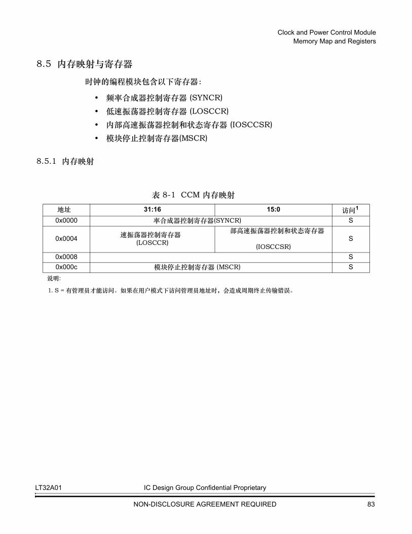
Clock and Power Control Module Memory Map and Registers
8.5 内存映射与寄存器
时钟的编程模块包含以下寄存器:
• 频率合成器控制寄存器 (SYNCR)
• 低速振荡器控制寄存器 (LOSCCR)
• 内部高速振荡器控制和状态寄存器 (IOSCCSR)
• 模块停止控制寄存器(MSCR)
8.5.1 内存映射
表 8-1 CC M 内存映射
地址 31:16 15:0 访问1
0x0000 率合成器控制寄存器(SYNCR) S
0x0004 速振荡器控制寄存器(LOSCCR)
部高速振荡器控制和状态寄存器
(IOSCCSR)S
0x0008 S0x000c 模块停止控制寄存器 (MSCR) S
说明:
1. S = 有管理员才能访问。如果在用户模式下访问管理员地址时,会造成周期终止传输错误。
LT32A01 IC Design Group Confidential Proprietary
NON-DISCLOSURE AGREEMENT REQUIRED 83

Clock and Power Control Module Memory Map and Registers
8.5.2 寄存器描述
本小节对时钟模块寄存器进行了描述。
8.5.2.1 合成器的控制寄存器
合成器的控制寄存器总是可读/写的。
图 8-1 合成器的控制寄存器 (SYNCR)
SYSDIV[5:0] — 系统时钟分频器该位为系统时钟设置分频值。默认的分频值是 6’b000000,其他分频值如表8-2所示。
寄存器偏移地址 : 0x00031 30 29 28 27 26 25 24
R ENLOW-POWER 0
WRESET: 0 0 0 0 0 0 0 0
23 22 21 20 19 18 17 16R
SYSDIV[5:0] IPSDIV[1:0]W
RESET: 0 0 0 0 0 0 0 1
15 14 13 12 11 10 9 8R
ADCDIV[3:0] LOSCEN0 0
SLEEPW
RESET: 0 0 1 0 1 0 0 0
7 6 5 4 3 2 1 0R
CLKOUTSEL[1:0] STBYMD[1:0]0
ADCEN FLSLPE LOSCLPEW
RESET: 0 0 1 1 0 1 1 1
= Writes have no effect and the access terminates without a transfer error exception.
表 8-2 系统时钟分频器SYSDIV[5:0] 分频值
000000 Divide-by-1000001 Divide-by-2000010 Divide-by-3000011 Divide-by-4000100 Divide-by-5
LT32A01 IC Design Group Confidential Proprietary
NON-DISCLOSURE AGREEMENT REQUIRED 84

Clock and Power Control Module Memory Map and Registers
IPSDIV[1:0] — IPS 时钟分频器该位为IPS时钟设置了分频值。默认的分频值是2’b01。其他的分频值参考 表8-3。
ADCDIV[3:0] — ADC 时钟分频器该位为ADC时钟分频器设置分频值。默认的分频是为4’b0000 其他分频值参考表8-4。
000101 Divide-by-6... ...... ...... ...
111100 Divide-by-61111101 Divide-by-62111110 Divide-by-63111111 Divide-by-64
表 8-3 IPS C时钟分频器IPSDIV[1:0] 分频值
00 Divide-by-101 Divide-by-210 Divide-by-311 Divide-by-4
表 8-4 ADC 时钟分频器ADCDIV[3:0] 分频值
0000 Divide-by-10001 Divide-by-20010 Divide-by-30011 Divide-by-40100 Divide-by-50101 Divide-by-60110 Divide-by-70111 Divide-by-81000 Divide-by-91001 Divide-by-101010 Divide-by-111011 Divide-by-121100 Divide-by-131101 Divide-by-14
表 8-2 系统时钟分频器SYSDIV[5:0] 分频值
LT32A01 IC Design Group Confidential Proprietary
NON-DISCLOSURE AGREEMENT REQUIRED 85

Clock and Power Control Module Memory Map and Registers
LOSCEN — 内部低速128KHz振荡器使能位1 = 内部低速128KHz振荡器使能0 = 内部低速128KHz振荡器禁止
SLEEP — 芯片休眠模式控制位设定SLEEP位,芯片进入待机模式,其他操作是无效的。
CLKOUTSEL[1:0] — 时钟选择位
STBYMD[1:0] — 待机操作控制位
STBYMD[1:0] 控制着待机模式下的时钟源,系统时钟操作和LDO的状态。具体如 表8-6所示。
FLSLPE —Flash 低功耗使能如果置位了FLSLPE ,那么 EFLASH会在芯片进入待机模式期间进入待机模式。
1 = EFLASH的低功耗模式使能0 = EFLASH的低功耗模式禁止
LOSCLPE — 内部低速128KHz振荡器低功耗使能
1110 Divide-by-151111 Divide-by-16
表 8-5 CLKOUTSEL 模块CLKOUTSEL[1:0] 时钟
00 System clock01 128KHZ clock10 Disable11 Disable
表 8-6 待机模式下的待机操作控制位待机模式下的操作
STBYMD ADC 时钟 系统时钟 时钟源 LDO00 Enable Disabled Enable Normal01 Disabled Disabled Enable Normal10 Disabled Disabled Disabled Normal11 Disabled Disabled Disabled Standby
表 8-4 ADC 时钟分频器ADCDIV[3:0] 分频值
LT32A01 IC Design Group Confidential Proprietary
NON-DISCLOSURE AGREEMENT REQUIRED 86

Clock and Power Control Module Memory Map and Registers
如果置位了 LOSCLPE,那么芯片在待机模式时,内部低速128KHz振荡器会停 止。
1 = 内部低速128KHz振荡器低功耗使能0 = 内部低速128KHz振荡器低功耗禁止
ADCEN — 模数转换器时钟使能位1 = ADC 时钟使能0 = ADC 时钟禁止
ENLOWPOWER — 进入低功耗模式状态使能位系统进入待机模式之前,要确保该位是明确的,否则不会成功进入低功耗模式。 从低功耗模式恢复后,该位会被置位,并且进入低功耗模式后,该位会被硬件清零。
1 = 允许进入低功耗模式0 = 禁止进入低功耗模式
LT32A01 IC Design Group Confidential Proprietary
NON-DISCLOSURE AGREEMENT REQUIRED 87

Clock and Power Control Module Memory Map and Registers
8.5.2.2 内部高速振荡器的控制和状态寄存器
寄存器偏移地址 : 0x0004
图8-2 内部高速振荡器的控制和状态寄存器 (IOSCCSR)
LOSCST[4:0] — 内部低速振荡器稳定时间值
The internal low speed oscillator will wait LOSCST[4:0] cycles of 128KHZ oscillator and then output clock after switch on.
31 30 29 28 27 26 25 24R TEST1 TEST0 0 0 0 0 0 0W
RESET: 0 0 0 0 0 0 0 0
23 22 21 20 19 18 17 16R 0 0 0 0 0
LOSCST[4:2]W
RESET: 0 0 0 0 0 1 1 1
15 14 13 12 11 10 9 8R
LOSCST[1:0]0 0 0 0 0 0
WRESET: 1 1 0 0 0 0 0 0
7 6 5 4 3 2 1 0R 0 0 0 0 0 0 0 0W
RESET: 0 0 0 0 0 0 0 0
= Writes have no effect and the access terminates without a transfer error exception.
LT32A01 IC Design Group Confidential Proprietary
NON-DISCLOSURE AGREEMENT REQUIRED 88

Clock and Power Control Module Memory Map and Registers
8.5.2.3 模块停止控制寄存器
模块停止控制寄存器(MSCR) 总是可读/写的。
寄存器偏移地址 : 0x000c
图 8-3 模块停止控制寄存器 (MSCR)
MS[20:0] — 模块停止位MS[20:0]位禁止模块时钟运行在最高水平。(详情见表8-7中MS[15:0]位对应的模块。)
1 = 模块时钟禁止0 = 模块时钟使能
31 30 29 28 27 26 25 24R 0 0 0 0 0 0 0 0W
RESET: 0 0 0 0 0 0 0 0
23 22 21 20 19 18 17 16R 0 0 0
MS[20] MS[19] MS[18] MS[17] MS[16]W
RESET: 0 0 0 0 0 0 0 0
15 14 13 12 11 10 9 8R
MS[15] MS[14] MS[13] MS[12] MS[11] MS[10] MS[9] MS[8]W
RESET: 0 0 0 0 0 0 0 0
7 6 5 4 3 2 1 0R
MS[7] MS[6] MS[5] MS[4] MS[3] MS[2] MS[1] MS[0]W
RESET: 0 0 0 0 0 0 0 0
= Writes have no effect and the access terminates without a transfer error exception.
表 8-7 MS[15:0] 位对应的模块MS Bit Corresponding Module
0 CPM1 SCI12 Reserved3 ADC4 PIT05 PIT16 PIT2
LT32A01 IC Design Group Confidential Proprietary
NON-DISCLOSURE AGREEMENT REQUIRED 89

Clock and Power Control Module Memory Map and Registers
7 PIT38 Reserved9 SPI
10 PWM011 PWM112 EPORT013 EPORT114 LDMAC15 EFM16 RESET17 WDT18 SCI019 CCM20 i2c
表8-7 MS[15:0] 位对应的模块MS Bit Corresponding Module
LT32A01 IC Design Group Confidential Proprietary
NON-DISCLOSURE AGREEMENT REQUIRED 90

Clock and Power Control Module Memory Map and Registers
8.5.2.4 EPT 外部时钟源使能控制寄存器
寄存器地址 : 0x0010
图 8-4 EPT 外部时钟源使能控制寄存器(ECSECR)
EPTDIV[50] — EPT 时钟分频器该位为EPT时钟设置了分频值。默认的分频值是8’h80。其他分频值请参考 表8-8。
31 30 29 28 27 26 25 24R
EPTDIV[7:0]W
RESET: 1 0 0 0 0 0 0 0
23 22 21 20 19 18 17 16R
EPTEN0 0 0 0 0 0 0
WRESET: 0 0 0 0 0 0 0 0
15 14 13 12 11 10 9 8R 0W
RESET: 0 0 0 0 0 0 0 0
7 6 5 4 3 2 1 0R 0W
RESET: 0 0 0 0 0 0 0 0
= Writes have no effect and the access terminates without a transfer error exception.
表 8-8 EPT 时钟分频器EPTDIV[8:0] Divide Value
00000000 Divide-by-100000001 Divide-by-200000010 Divide-by-300000011 Divide-by-400000100 Divide-by-500000101 Divide-by-6
... ...
... ...
... ...11111110 Divide-by-25511111111 Divide-by-256
LT32A01 IC Design Group Confidential Proprietary
NON-DISCLOSURE AGREEMENT REQUIRED 91

Clock and Power Control Module Memory Map and Registers
EPTEN — EPT 时钟使能位如果EPTEN位置1,那么EPT时钟会从系统时钟中分频得到。
1 = EPT 时钟使能0 = EPT 时钟禁止
LT32A01 IC Design Group Confidential Proprietary
NON-DISCLOSURE AGREEMENT REQUIRED 92

Clock and Power Control Module Memory Map and Registers
8.5.2.5 OSC BIST测试配置寄存器1
寄存器地址 : 0x0014
图 8-5 OSC BIST测试配置寄存器1(OBTCR1)
BIST_HOLD_TARGET — BIST CLK HOLD COUNT TARGET VALUEWAIT CLK UNDER TEST STABLE AFTER TRIM VALUE CHANGE
BIST_ TARGET — BIST时钟计数的目标值
31 30 29 28 27 26 25 24R
BIST_HOLD_TARGET[15:8]W
RESET: 0 0 0 0 0 0 0 0
RBIST_HOLD_TARGET[7:0]
WRESET: 0 0 0 0 0 0 0 0
15 14 13 12 11 10 9 8R
BIST_TARGET[15:0]W
RESET: 0 0 0 0 0 0 0 0
7 6 5 4 3 2 1 0R
BIST_TARGET[7:0]W
RESET: 0 0 0 0 0 0 0 0
= Writes have no effect and the access terminates without a transfer error exception.
LT32A01 IC Design Group Confidential Proprietary
NON-DISCLOSURE AGREEMENT REQUIRED 93

Clock and Power Control Module Memory Map and Registers
8.5.2.6 OSC BIST测试配置寄存器2
寄存器地址 : 0x0018
图 8-6 OSC BIST测试配置寄存器2(OBTCR2)
BIST_TEST_TARGET — UNDER TEST CLK COUNT TARGET VALUE
BIST_TEST_CTRIM_MARGIN — UNDER TEST CLK COUNT ERROR MARGIN FOR COARSE TRIM
31 30 29 28 27 26 25 24R
BIST_TEST_TARGET[15:8]W
RESET: 0 0 0 0 0 0 0 0
RBIST_TEST_TARGET[7:0]
WRESET: 0 0 0 0 0 0 0 0
15 14 13 12 11 10 9 8R
BIST_TEST_CTRIM_MARGIN[15:0]W
RESET: 0 0 0 0 0 0 0 0
7 6 5 4 3 2 1 0R
BIST_TEST_CTRIM_MARGIN[7:0]W
RESET: 0 0 0 0 0 0 0 0
= Writes have no effect and the access terminates without a transfer error exception.
LT32A01 IC Design Group Confidential Proprietary
NON-DISCLOSURE AGREEMENT REQUIRED 94

Clock and Power Control Module Memory Map and Registers
8.5.2.7 OSC BIST测试控制寄存器
寄存器地址 : 0x001c
图 8-7 OSC BIST测试控制寄存器(OBTCR)
BIST_TEST_FTRIM_MARGIN — UNDER TEST CLK COUNT ERROR MARGIN FOR FINE TRIM
BIST_MODE — BIST 模式
1 = 跟踪模式0 = 配平模式
BIST_START — BIST开始
1 = 开始0 = 停止
BIST_VAL_INV — BIST配平位取反
1 = 取反0 = 正常
BIST_IRC_SEL — FIRC or SIRC bist selection
31 30 29 28 27 26 25 24R
BIST_TEST_FTRIM_MARGIN[15:8]W
RESET: 0 0 0 0 0 0 0 0
RBIST_TEST_FTRIM_MARGIN[7:0]
WRESET: 0 0 0 0 0 0 0 0
15 14 13 12 11 10 9 8R BIST_STA
RTBIST_MO
DEBIST_VAL
_INVBIST_IRC_
ENBIST_IRC_
SEL BIST_ENW
RESET: 0 0 0 0 0 0 1 0
7 6 5 4 3 2 1 0R 0 0 0 0 0 0 0 0W
RESET: 0 0 0 0 0 0 0 0
= Writes have no effect and the access terminates without a transfer error exception.
LT32A01 IC Design Group Confidential Proprietary
NON-DISCLOSURE AGREEMENT REQUIRED 95

Clock and Power Control Module Memory Map and Registers
1 = FIRC bist0 = SIRC bist
BIST_EN — UNDER TEST CLK ENABLE
1 = 使能0 = 禁止
8.5.2.8 OSC BIST 测试计数器寄存器
寄存器地址 : 0x0020
图 8-8 OSC BIST测试计数器寄存器(OBTCNTR)
BIST_CTRIM_TRACE — BIST CTRIM TRACE VALUE
BIST_FTRIM_TRACE — BIST FTRIM TRACE VALUE
BIST_TEST_CNT — BIST TEST COUNTER VALUE
31 30 29 28 27 26 25 24R BIST_TEST_CNT[15:8]W
RESET: 0 0 0 0 0 0 0 0
23 22 21 20 19 18 17 16R BIST_TEST_CNT[7:0]W
RESET: 0 0 0 0 0 0 0 0
15 14 13 12 11 10 9 8R
BIST_CTRIM_TRACE[4:0]W
RESET: 0 0 0 0 0 0 0 0
7 6 5 4 3 2 1 0R
BIST_FTRIM_TRACE[4:0]W
RESET: 0 0 0 0 0 0 0 0
= Writes have no effect and the access terminates without a transfer error exception.
LT32A01 IC Design Group Confidential Proprietary
NON-DISCLOSURE AGREEMENT REQUIRED 96
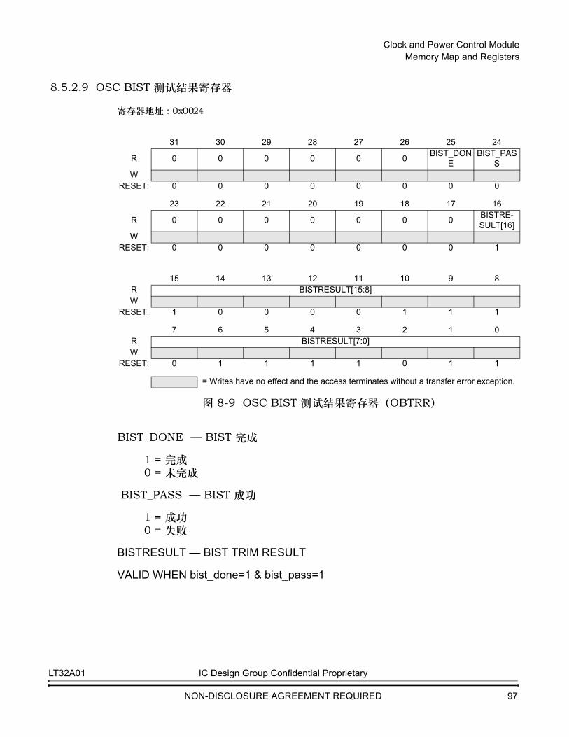
Clock and Power Control Module Memory Map and Registers
8.5.2.9 OSC BIST 测试结果寄存器
寄存器地址 : 0x0024
图 8-9 OSC BIST 测试结果寄存器(OBTRR)
BIST_DONE — BIST 完成
1 = 完成0 = 未完成
BIST_PASS — BIST 成功
1 = 成功0 = 失败
BISTRESULT — BIST TRIM RESULT
VALID WHEN bist_done=1 & bist_pass=1
31 30 29 28 27 26 25 24
R 0 0 0 0 0 0 BIST_DONE
BIST_PASS
WRESET: 0 0 0 0 0 0 0 0
23 22 21 20 19 18 17 16
R 0 0 0 0 0 0 0 BISTRE-SULT[16]
WRESET: 0 0 0 0 0 0 0 1
15 14 13 12 11 10 9 8R BISTRESULT[15:8]W
RESET: 1 0 0 0 0 1 1 1
7 6 5 4 3 2 1 0R BISTRESULT[7:0]W
RESET: 0 1 1 1 1 0 1 1
= Writes have no effect and the access terminates without a transfer error exception.
LT32A01 IC Design Group Confidential Proprietary
NON-DISCLOSURE AGREEMENT REQUIRED 97

Reset Controller Module Overview
第九节:复位控制器模块
9.1 概述
复位控制器拥可以判断引起复位的原因,并将适当的复位信号传输给系统,然后保存所有引起复位的事件。
9.2 特性
该模块的特性包括:
• 4个复位源:
–上电复位
–外部引脚引起的复位
–软件复位
–看门狗定时器复位
–可编程的电压检测复位
• 软件可读状态标志指示上次复位的原因
LT32A01 IC Design Group Confidential Proprietary
NON-DISCLOSURE AGREEMENT REQUIRED 98

Reset Controller Module Block Diagram
9.3 框图
复位控制器的结构如图9-1所示。
图 9-1 复位控制器框图
Reset
Controller
External External
POR
WDT Timeout
SOFTWARE RESET
To INTERNAL RESETS
POR
PVD RESET
On Chip
Exernal reset
LT32A01 IC Design Group Confidential Proprietary
NON-DISCLOSURE AGREEMENT REQUIRED 99

Reset Controller Module Memory Map and Registers
9.4 内存映射和寄存器
复位控制器可编程模块包含以下寄存器:
• 复位控制寄存器 (RCR)——选择复位控制器功能
• 复位状态寄存器 (RSR)——反映了最后一个复位源状态
地址映射和寄存器的描述如表9-1所示。
表 9-1 复位控制器地址映射
地址 位 7:0 访问1
说明:
1. S/U = 管理者模式和用户模式下都可访问。
0x0000 保留 S/U0x0001 RTR—复位测试寄存器 S/U0x0002 RSR—复位状态寄存器 S/U0x0003 RCR—复位控制寄存器 S/U
LT32A01 IC Design Group Confidential Proprietary
NON-DISCLOSURE AGREEMENT REQUIRED 100
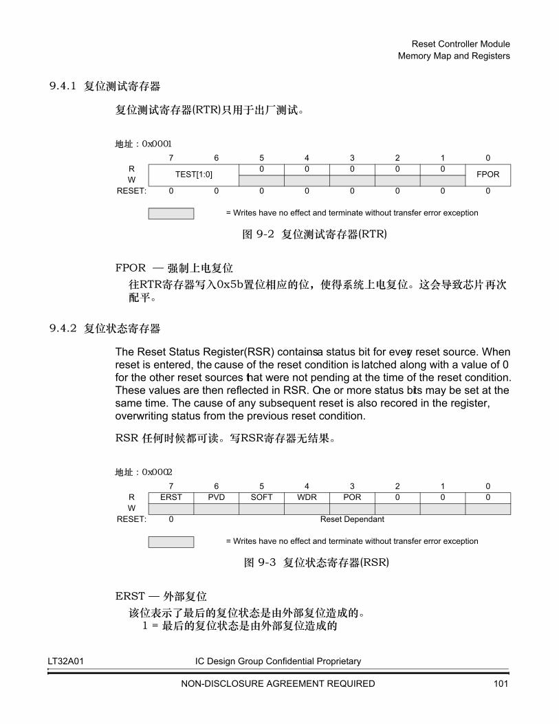
Reset Controller Module Memory Map and Registers
9.4.1 复位测试寄存器
复位测试寄存器(RTR)只用于出厂测试。
图 9-2 复位测试寄存器(RTR)
FPOR — 强制上电复位往RTR寄存器写入0x5b置位相应的位,使得系统上电复位。这会导致芯片再次 配平。
9.4.2 复位状态寄存器
The Reset Status Register(RSR) contains a status bit for every reset source. When reset is entered, the cause of the reset condition is latched along with a value of 0 for the other reset sources that were not pending at the time of the reset condition. These values are then reflected in RSR. One or more status bits may be set at the same time. The cause of any subsequent reset is also recored in the register, overwriting status from the previous reset condition.
RSR 任何时候都可读。写RSR寄存器无结果。
图 9-3 复位状态寄存器(RSR)
ERST — 外部复位该位表示了最后的复位状态是由外部复位造成的。
1 = 最后的复位状态是由外部复位造成的
地址 : 0x00017 6 5 4 3 2 1 0
RTEST[1:0]
0 0 0 0 0FPOR
WRESET: 0 0 0 0 0 0 0 0
= Writes have no effect and terminate without transfer error exception
地址 : 0x00027 6 5 4 3 2 1 0
R ERST PVD SOFT WDR POR 0 0 0W
RESET: 0 Reset Dependant
= Writes have no effect and terminate without transfer error exception
LT32A01 IC Design Group Confidential Proprietary
NON-DISCLOSURE AGREEMENT REQUIRED 101

Reset Controller Module Memory Map and Registers
0 = 最后的复位状态不是由外部复位造成的
PVD — 可编程的电压检测该位表示了最后的复位状态是由PVD复位造成的。
1 = 最后的复位状态是由PVD复位造成的0 = 最后的复位状态不是由PVD复位造成的
SOFT — 软件复位标志该位表示了最后的复位状态是由软件造成的。
1 = 最后的复位状态是由软件造成的。0 = 最后的复位状态不是由软件造成的.
WDR —看门狗定时器复位标志该位表示了最后的复位状态是由看门狗定时器复位造成的。
1 = 最后的复位状态是由看门狗定时器复位造成的。0 = 最后的复位状态不是由看门狗定时器复位造成的
POR — 上电复位标志该位表示了最后的复位状态是由上电复位造成的。
1 = 最后的复位状态是由上电复位造成的。0 = 最后的复位状态不是由上电复位造成的。
LT32A01 IC Design Group Confidential Proprietary
NON-DISCLOSURE AGREEMENT REQUIRED 102

Reset Controller Module Functional Description
9.4.3 复位控制寄存器
复位控制寄存器(RCR)允许软件控制请求复位。
图 9-4 复位控制寄存器(RCR)
FRCRSTOUT — Force RSTOUT PinThe FRCRSTOUT bit allows software to assert or negate the external RSTOUT pin.
1 = Assert RSTOUT pin0 = Negate RSTOUT pin
9.5 功能描述
9.5.1 复位源
表9-2中定义了各复位源和复位控制器的驱动信号。
地址 : 0x00037 6 5 4 3 2 1 0
R 0 0 0 0 0 0 0 FRCR-STOUTW
RESET: 0 0 0 0 0 0 0 0
= Writes have no effect and terminate without transfer error exception
表 9-2 复位源汇总
源 类型
POR 异步
ERST 异步
Watchdog timer 异步
Software 同步
PVD 异步
LT32A01 IC Design Group Confidential Proprietary
NON-DISCLOSURE AGREEMENT REQUIRED 103

Reset Controller Module Functional Description
为了保护数据的完整性,同步复位源不会被复位控制逻辑激活,直到当前总线循环结束。等到循环结束后,复位系统时钟的下一个上升沿到来时,复位才会被执行。 任何时候,复位控制逻辑必须与总线周期循环结束后的复位同步,并且内部总线监视器自动启用。
异步复位源通常表明灾难性故障。因此,复位控制逻辑不需要等待当前总线周期完成。系统马上执行复位。
9.5.1.1 上电复位 (POR)
上电时,复位控制器发出系统复位。系统复位继续进行,直到POR已达到最低可接受水平。
9.5.1.2 看门狗定时器复位
看门狗定时器超时后引起定时器复位请求被识别和锁存。
9.5.1.3 软件复位
如果SYSRESTEQ位在C0处理器的嵌入式中断控制器(EIC)中被置位了,那么软件复位将会发生。复位控制器发出约2048个周期的系统复位。最后退出复位,恢复运行。
9.5.1.4 可编程的电压检测复位
当嵌入式闪存模块中的CCR寄存器里的PVDRE位被置位了,并且VDD超过了PVD阈值,那么,PVD将产生复位。
LT32A01 IC Design Group Confidential Proprietary
NON-DISCLOSURE AGREEMENT REQUIRED 104
X84L
线条
X84L
线条

Reset Controller Module Functional Description
9.5.2 复位控制流程
复位逻辑控制流如图9-5所示。所有给出的周期数都是近似的。
图 9-5 复位控制流程
WDT TIMEOUTor SW RESET?
N
ENABLE BUS MONITOR
BUS CYCLECOMPLETE?
LATCH RESET STATUS LATCH RESET STATUS
POR or LVD
N
Y
RESET NEGATED ?N
WAIT 2048 CLOCK CYCLES
Y
Y
RCON ASSERTED ? WAIT 512 CLKOUT CYCLESYN
LT32A01 IC Design Group Confidential Proprietary
NON-DISCLOSURE AGREEMENT REQUIRED 105

Static Random Access Memory (SRAM) Introduction
LT32A01 IC Design Group Confidential Proprietary
NON-DISCLOSURE AGREEMENT REQUIRED 106
第十节:静态随机存储器(SRAM)
10.1 说明
静态随机存储器(SRAM)的特性如下所示:
• 片内4K字节 SRAM
• 固定的地址空间
• 字节,半字(16位),或字(32位)的读/写访问
• 访问一次需要一个时钟(包括字节、半字与字)
• 管理者或用户访问模式
10.2 操作模式
访问SRAM是不受任何方式限制,不管是管理者模式或是用户模式都可以访问。
10.3 低功耗模式
在等待、休眠和停止模式中,SRAM的时钟是禁止的。退出这些模式时不需要恢复时间。
10.4 复位操作
The SRAM contents are undefined immediately following a power-on reset. SRAM contents are unaffected by system reset. If a synchronous reset occurs during a read or write access, then the access completes normally and any pipelined access in progress is stopped without corruption of the SRAM contents.
10.5 中断
SRAM模块不产生中断请求。

Advance Information — LT32A01
第十一节:嵌入式闪存模块(EFLASH)
11.1 说明
The Embedded FLASH(EFM) is a CMOS sector erase, byte(8-bit) program.It is organized as 32K Bytes main array with five Non-Volatile Register sectors (NVR) (512 Bytes each).The sector erase operation erases all bytes within a sector(512bytes).
The Flash IP device writes (program or erase) with a 1.5 Volt typical power supply.Program and erase operations are performed under CPU control through a command driven interface to an internal state machine. It is not permitted to read from a FLASH physical block while the block is being programmed or erased.
11.2 特性
EFM的特性如下所示:
• 32K字节(主阵列)+ 1.5K字节(5个NVR扇区)闪存
• 30 MHz 的单周期字节读取。对齐半字(16位)和字(32位)。
• 自动编程和擦除操作
• 可选的指令完成中断
• 为防止意外编程或擦除操作的灵活方案
• 单片机的应用程序的安全
• 单电源供电(系统VDD)用于所有模块的操作
11.3 操作模式
EFM 有2种操作模式:
1. 闪存用户模式 — 在这种模式下,EFM用于非易失性的程序和数据存储。Flash编程和擦除操作是通过用户软件控制。
2. 闪存 STB 模式— 该模式只用于出厂时的EFM测试。
是指为说明Flash用户模式操作。
IC Design Group Confidential Proprietary
NON-DISCLOSURE AGREEMENT REQUIRED 107

Embedded Flash Module
11.4 框图
图 11-1 EFM 框图
IPBUS
AHB Bus
IPBus Interface
8Kx32Block
Control Register
Common Registers
Flash Interface
C0 Interface
30 Sep 2011 — Rev 0.1 IC Design Group Confidential Proprietary LT32A01
108 NON-DISCLOSURE AGREEMENT REQUIRED

Embedded Flash Module Module Memory Map
11.5 模块内存映射
当BOOT=1时,Flash的主阵列映射从地址0x0000_0000开始。
当BOOT=0时,Flash的NVR阵列映射从地址0x0000_0000开始。
图11-2和11-3分别展示了Flash的主阵列和NVR阵列的地址映射。
图 11-2 EFM 阵列内存映射(BOOT=1)
0x0000_0000
0x0040_0000
0x0000_7FFF Main Array
0x0040_05FF
0xFFFF_FFFF
NVR Sector
LT32A01 IC Design Group Confidential Proprietary
NON-DISCLOSURE AGREEMENT REQUIRED 109

Embedded Flash Module
图 11-3 EFM 阵列内存映射(BOOT=0)
0x0000_00000x0000_05FF
Main Array
0xFFFF_FFFF
NVR Sector
0x0040_0000
0x0040_7FFF
IC Design Group Confidential Proprietary
110 NON-DISCLOSURE AGREEMENT REQUIRED

Embedded Flash Module Module Memory Map
EFM模块还包含一组控制和状态寄存器。这些寄存器的内存映射表11-1所示。
表 11-1 寄存器内存映射
地址偏移 位 31-24 位 23-16 位 15-8 位 7-0 访问1,2
0x0000 EFMCR S0x0004 EFMSEC0 S0x0008 EFMSEC1 S0x000c EFMSEC2 S0x0010 EFMTIM0 S0x0014 EFMTIM1 S
0x0018 EFMCMD 保留3 EFMSTAT 保留 S
说明:
1. S = 只能被CPU管理者模式访问。
2. 若在用户模式下访问只能在管理者模式下访问的地址,会造成周期终止传输错误。
3. 往保留的地址里写数据是没有效果的,而读保留的地址的数据时返回的是0。
LT32A01 IC Design Group Confidential Proprietary
NON-DISCLOSURE AGREEMENT REQUIRED 111

Embedded Flash Module
11.6 寄存器描述
11.6.1 EFM 配置寄存器(EFMCR)
EFM配置寄存器 (EFMCR)是 unbanked,并且是用于配置和控制EFM阵列的操作以及总线接口单元(BIU)。
图 11-4 EFM 配置寄存器(EFMCR)
DIVSEL[5:0] — 时钟分频器选择DIVSEL[5:0]可以有效地将EFM的输入时钟分频降至约1MHz频率。EFM的分频时钟频率=ipg_clk的频率/(DIVSEL[5:0] +1)。DIVSEL[5:0]= 0时意味着EFM的分频时钟频率=ipg_clk 的频率。为了使得Tpgs的最小值哟足够的裕度和最大值等于0.7us,ipg_clk 的频率不得低于1.5MHz。
VREAD0 — VREA D0 闪存功能使能1 = 使能 VREAD0 0 = 禁止 VREAD0
VREAD1 — VREA D1 闪存功能使能1 = 使能 VREAD10 = 禁止 VREAD1
地址偏移: 0x0000 31 30 29 28 27 26 25 24
R 0 0DIVSEL[5:0]
WRESET: 0 0 0 1 1 0 0 0
23 22 21 20 19 18 17 16R 0 0 0 0 0 0
VREAD0 VREAD1W
RESET: 0 0 0 0 0 0 0 0
15 14 13 12 11 10 9 8R 0
CEBATS[2:0]0
OEBATS[2:0]W
RESET: 0 0 0 1 0 0 1 0
7 6 5 4 3 2 1 0R 0 0 0 0
WS[3:0]W
RESET: 0 0 0 0 1 1 1 1
= Writes have no effect and the access terminates without a transfer error exception.
IC Design Group Confidential Proprietary LT32A01
112 NON-DISCLOSURE AGREEMENT REQUIRED

Embedded Flash Module Register Descriptions
CEBATS[2:0]— CEb Signal Assert Timing SelectThese bits select the assertion timing of CEb when the operation is read or write the configuration registers. See functional description for details.
OEBATS[2:0]— OEb Signal Assert Timing SelectThese bits select the assertion timing of OEb when the operation is read. See functional description for detail
WS[3:0] — 等待状态位当闪存的地址匹配时,WS[3:0]决定了等待状态的次数。
Figure 11-5 CEb/OEb Assert Timing
CLK
CEB
OEB
rws+1
Tass
Tass
LT32A01 IC Design Group Confidential Proprietary
NON-DISCLOSURE AGREEMENT REQUIRED 113

Embedded Flash Module
Table 11-2 Assert and Negate Timing (Unit : system cycle)OEBATS[2:0]/CEBATS[
2:0] Assert Time (Tass)
000 0001 1/2010 2/2011 3/2100 4/2101 5/2110 6/2111 7/2
IC Design Group Confidential Proprietary LT32A01
114 NON-DISCLOSURE AGREEMENT REQUIRED

Embedded Flash Module Register Descriptions
11.6.2 EFM 读安全寄存器0 (EFMSEC0)
EFM 读安全寄存器0(EFMSEC0)是用来存储第一个和第二个RDN信息的。
图 11-6 EFMSEC0
RDN1EN — 决定 RDN1 (第一冗余扇区)是否是用于修复坏扇区1 = RDN1 的修复功能使能 0 = RDN1 的修复功能禁止
RDN1INFO[7:0] — RDN1修复信息这8位信息指示了需要RDN1修复的坏扇区地址。
RDN2EN — 决定 RDN2 (第二冗余扇区)是否是用于修复坏扇区1 = RDN2 的修复功能使能 0 = RDN2 的修复功能禁止
RDN2INFO[7:0] — RDN2 修复信息
这8位信息指示了需要RDN2修复的坏扇区地址。
地址偏移: 0x0004 31 30 29 28 27 26 25 24
R 0 0 0 0 0 0 0 RDN1ENW
23 22 21 20 19 18 17 16R RDN1INFO[7:0]W
15 14 13 12 11 10 9 8R 0 0 0 0 0 0 0 RDN2ENW
7 6 5 4 3 2 1 0R RDN2INFO[7:0]W
RE-SET1
说明:
1. 复位值是由NVR5阵列中的RDN信息决定的。
= Writes have no effect and the access terminates without a transfer error exception.
LT32A01 IC Design Group Confidential Proprietary
NON-DISCLOSURE AGREEMENT REQUIRED 115

Embedded Flash Module
11.6.3 EFM 读安全寄存器1 (EFMSEC1)
EFM 读安全寄存器(EFMSEC1) 用于存储第三个和第四个RDN信息。
图 11-7 EFMSEC1
RDN3EN — 决定 RDN3(第三冗余扇区)是否是用于修复坏扇区1 = RDN3 的修复功能使能0 = RDN3 的修复功能禁止
RDN3INFO[7:0] — RDN 3修复信息该8位信息指示了需要RDN3修复的坏扇区地址。
RDN4EN — 决定 RDN4(第四冗余扇区)是否是用于修复坏扇区1 = RDN4 的修复功能使能0 = RDN4 的修复功能禁止
RDN4INFO[7:0] — RDN4 修复信息
该8位信息指示了需要RDN4修复的坏扇区地址。
地址偏移: 0x0008 31 30 29 28 27 26 25 24
R 0 0 0 0 0 0 0 RDN3ENW
23 22 21 20 19 18 17 16R RDN3INFOW
15 14 13 12 11 10 9 8R 0 0 0 0 0 0 0 RDN4ENW
7 6 5 4 3 2 1 0R RDN4INFOW
RE-SET1
说明:
1. 复位值是由NVR5阵列中的RDN信息决定的。
= Writes have no effect and the access terminates without a transfer error exception.
IC Design Group Confidential Proprietary LT32A01
116 NON-DISCLOSURE AGREEMENT REQUIRED

Embedded Flash Module Register Descriptions
11.6.4 EFM 读安全寄存器2 (EFMSEC2)
EFM读安全寄存器2(EFMSEC2)是用于存储第一个和第二个RDN信息的。
图 11-8 EFMSEC2
RDN5EN — 决定 RDN5(第五冗余扇区)是否是用于修复坏扇区1 = RDN5 的修复功能使能0 = RDN5 的修复功能禁止
RDN5INFO[7:0] — RDN5 修复信息复位信息指示了需要RDN5修复的坏扇区地址。
地址偏移: 0x000c31 30 29 28 27 26 25 24
R 0 0 0 0 0 0 0 RDN5ENW
23 22 21 20 19 18 17 16R RDN5INFOW
15 14 13 12 11 10 9 8R 0 0 0 0 0 0 0 0W
7 6 5 4 3 2 1 0R 0 0 0 0 0 0 0 0W
RE-SET1
说明:
1. 复位值是由NVR4阵列中的RDN信息决定的。
= Writes have no effect and the access terminates without a transfer error exception.
LT32A01 IC Design Group Confidential Proprietary
NON-DISCLOSURE AGREEMENT REQUIRED 117
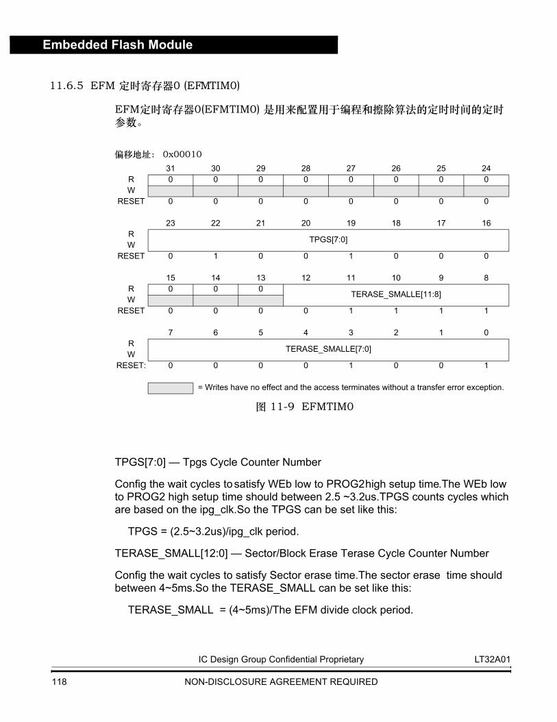
Embedded Flash Module
11.6.5 EFM 定时寄存器0 (EFMTIM0)
EFM定时寄存器0(EF MTIM0) 是用来配置用于编程和擦除算法的定时时间的定时参数。
图 11-9 EFMTIM0
TPGS[7:0] — Tpgs Cycle Counter Number
Config the wait cycles to satisfy WEb low to PROG2 high setup time.The WEb low to PROG2 high setup time should between 2.5 ~3.2 us.TPGS counts cycles which are based on the ipg_clk.So the TPGS can be set like this:
TPGS = (2.5~3.2us)/ipg_clk period.
TERASE_SMALL[12:0] — Sector/Block Erase Terase Cycle Counter Number
Config the wait cycles to satisfy Sector erase time.The sector erase time should between 4~5ms.So the TERASE_SMALL can be set like this:
TERASE_SMALL = (4~5ms)/The EFM divide clock period.
偏移地址: 0x0001031 30 29 28 27 26 25 24
R 0 0 0 0 0 0 0 0W
RESET 0 0 0 0 0 0 0 0
23 22 21 20 19 18 17 16R
TPGS[7:0]W
RESET 0 1 0 0 1 0 0 0
15 14 13 12 11 10 9 8R 0 0 0
TERASE_SMALLE[11:8]W
RESET 0 0 0 0 1 1 1 1
7 6 5 4 3 2 1 0R
TERASE_SMALLE[7:0]W
RESET: 0 0 0 0 1 0 0 1
= Writes have no effect and the access terminates without a transfer error exception.
IC Design Group Confidential Proprietary LT32A01
118 NON-DISCLOSURE AGREEMENT REQUIRED

Embedded Flash Module Register Descriptions
11.6.6 EFM 定时寄存器1 (EFMTIM1)
EFM定时寄存器1(EFMTIM1) 是用来配置用于编程和擦除算法的定时时间的定时参数。
图 11-10 EFMTIM1
TPROG[15:0] — Tprog Cycle Counter Number
Config the wait cycles to satisfy byte program time.The program time should between 6~7.5us.TPROG counts cycles which are based on the ipg_clk.So the TPROG can be set like this:
TPROG = (6~7.5us)/ipg_clk period.
TERASE[15:0] — Terase Cycle Counter Number
Config the wait cycles to satisfy Chip erase time.The minmum chip erase time is 30ms,and the maximum chip erase time is 40ms.so the TERASE can be set like this:
TERASE= (30ms~40ms)/The EFM divide clock period.
地址偏移: 0x0014
31 30 29 28 27 26 25 24R
TPROG[15:8]W
RESET 0 0 0 0 0 0 0 0
23 22 21 20 19 18 17 16R
TPROG[7:0]W
RESET 1 0 1 0 0 0 0 0
15 14 13 12 11 10 9 8R
TERASE[15:8]W
RESET 0 1 1 1 0 0 0 0
7 6 5 4 3 2 1 0R
TERASE[7:0]W
RESET: 1 0 1 0 1 1 0 1
= Writes have no effect and the access terminates without a transfer error exception.
LT32A01 IC Design Group Confidential Proprietary
NON-DISCLOSURE AGREEMENT REQUIRED 119
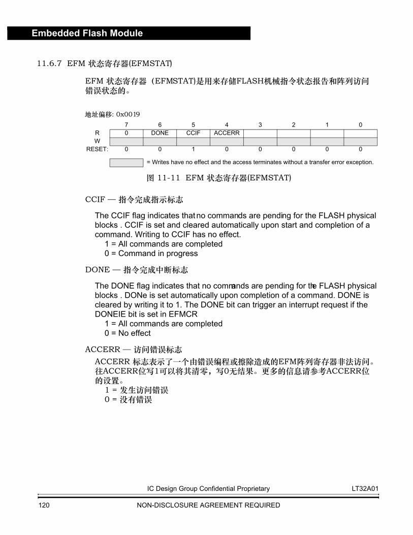
Embedded Flash Module
11.6.7 EFM 状态寄存器(EFMSTAT)
EFM 状态寄存器(EFMSTAT)是用来存储FLASH机械指令状态报告和阵列访问错误状态的。
图 11-11 EFM 状态寄存器(EFMSTAT)
CCIF — 指令完成指示标志
The CCIF flag indicates that no commands are pending for the FLASH physical blocks . CCIF is set and cleared automatically upon start and completion of a command. Writing to CCIF has no effect.
1 = All commands are completed 0 = Command in progress
DONE — 指令完成中断标志
The DONE flag indicates that no commands are pending for the FLASH physical blocks . DONe is set automatically upon completion of a command. DONE is cleared by writing it to 1. The DONE bit can trigger an interrupt request if the DONEIE bit is set in EFMCR
1 = All commands are completed0 = No effect
ACCERR — 访问错误标志ACCERR 标志表示了一个由错误编程或擦除造成的EFM阵列寄存器非法访问。往ACCERR位写1可以将其清零,写0无结果。更多的信息请参考ACCERR位的设置。
1 = 发生访问错误0 = 没有错误
地址偏移: 0x00197 6 5 4 3 2 1 0
R 0 DONE CCIF ACCERRW
RESET: 0 0 1 0 0 0 0 0
= Writes have no effect and the access terminates without a transfer error exception.
IC Design Group Confidential Proprietary LT32A01
120 NON-DISCLOSURE AGREEMENT REQUIRED

Embedded Flash Module Register Descriptions
11.6.8 EFM 命令寄存器 (EFMCMD)
图 11-12 EFMCMD
表 11-3 Flash 的有效指令
地址偏移: 0x0001b7 6 5 4 3 2 1 0
R 0CMD6 CMD5 CMD4 CMD3 CMD2 CMD1 CMD0
WRESET: 0 0 0 0 0 0 0 0
= Writes have no effect and the access terminates without a transfer error exception.
EFMCMD 含义 描述$20 编程 编写一段8/16/32位的程序$40 扇区擦除 擦除一个FLASH扇区(512字节)
$41 芯片擦除 擦除FLASH的块(32k字节主阵列)
LT32A01 IC Design Group Confidential Proprietary
NON-DISCLOSURE AGREEMENT REQUIRED 121

Embedded Flash Module
11.7 功能描述
11.7.1 编程和擦除操作
11.7.1.1 设置 EFMTIM0/1 寄存器
之前发布的任何编程或擦除的命令,写EFMTIM0/1时都必须在编程或擦除操作期间设置相应的参数。
11.7.1.2 编程,擦除和验证序列
This three-step command write sequence must be strictly followed. No intermediate writes to the EFM module are permitted between these three steps. The command write sequence is:
1. Read CCIF bit. If CCIF bit is set, the address, data, and command are ready for a new command sequence to begin.
2. Write the byte/half-word/word to be programmed to its location in the EFM array. The address and data will be stored in internal buffers. All address bits are valid for program commands. The value of the data written for verify and erase commands is ignored. For chip erase or verify, the address can be any location in the EFM array. For sector erase, address bits [8:0] are ignored.
3. Write the valid command to EFMCMD and lauch the command. CCIF will be cleared automatically when the command is launched.
When command execution is complete, the FLASH state machine will set the CCIF and DONE flag, indicating that the address, data, and command are ready for a new command sequence to begin.
DONE flag should be cleared before commencing another command write sequence.
The FLASH state machine will flag errors in command write sequences by means of the ACCERR flags in the EFMSTAT register. The ACCERR flags must be cleared before commencing another command write sequence.
11.7.1.3 闪存的非法操作
在写命令序列期间,如果发生了以下的非法操作,那么ACCERR将会被置位。
IC Design Group Confidential Proprietary LT32A01
122 NON-DISCLOSURE AGREEMENT REQUIRED

Embedded Flash Module Functional Description
1. 当命令序列忙时(CCIF = 0),写或者读EFM阵列将不起作用,并且还会置 位ACCERR;2. 当命令序列忙时(CCIF = 0),往 EFMCMD里写入新的命令将不起作用,
并且还会置位ACCERR。命令寄存器将不会被更新;
3. 当NVR1不被允许编程或擦除扇区时,若执意执行,命令不起作用,并且还会置位ACCERR;
4. 如果设置了密码,但输入密码不正确时,对NVR进行编程或者擦除扇区将不起作用,并且置位ACCERR;
5. 对NVR5进行编程或擦除扇区将会不起效果,并且置位ACCERR。
说明:
1. 如果使用了禁止 NVR编程/擦除功能或者禁止NVR5编程/擦除功能。
LT32A01 IC Design Group Confidential Proprietary
NON-DISCLOSURE AGREEMENT REQUIRED 123

Embedded Flash Module
IC Design Group Confidential Proprietary LT32A01
124 NON-DISCLOSURE AGREEMENT REQUIRED

Option Byte Register Memory Map
CCR
地址 : 0x001e
PVDC
第十二节:选项字节
12.1 寄存器的内存映射
表 12-1 寄存器内存映射
12.1.1 寄存器描述
12.1.1.1 PVDC— 可编程电压检测器配置寄存器
图 12-1 PVDC— 可编程电压检测器配置寄存器
地址偏移 位 31-24 位 23-16 位 15-8 位 7-0 访问1,2
0x001c S0x0020 IOSCST EOSCST S0x0024 PVDFEVR RFEVR S
0x002c FCR 保留3 S
0x0030 IOSTC S0x0034 LDOTC VREFTCR ADCCDISR S0x0038 MPUCONFR S0x003c GLFTC 保留 S
说明:
1. S = 只限于CPU管理者模式访问。
2. 在用户模式下访问只能在管理者模式下访问的地址,会造成周期终止传输错误。
3. 对保留的地址写入或者读取并不会有效果,并且返回0。
15 14 13 12 11 10 9 8Read: PVDF 0
PVDTEST[1:0] PVDOE PVDRE PVDIE PVDEWrite:
RESET: 0 0 0 0 0 0 0 1
7 6 5 4 3 2 1 0Read: 0 0 0 0 0
PVDC[2:0]Write:
RESET: 0 0 0 0 0 0 0 0
= Writes have no effect and the access terminates without a transfer error exception.
LT32A01 IC Design Group Confidential Proprietary
NON-DISCLOSURE AGREEMENT REQUIRED 125

Option Byte Register Memory Map
PVDTEST[1:0] — Write Access Enable Sequence Input
The PVDC register can not be changed,unless the correct sequence write in.The right sequence is :2’b01->2’b10->2’b11.After write these two bits following this sequence,these two bits’ value == 2’b11,then the PVDC register can be changed at will.Only writes 2’b00 can clear these two bits when the value equals to 2’b11.Writes other value has no effect and returns 2’b11.
PVDF— 可编程的电压检测器标志PVDF 表明 VDD比PVD的阈值要低,POR可以清除它。
1 = VDD 比 PVD的阈值低 0 = VDD不比P VD的阈值低
PVDOE— 可编程的电压检测器输出使能1 = PVD 输出使能0 = PVD 输出禁止
PVDE— 可编程电压检测器使能如果PVD使能了,那么PVDE就可配置。 POR可以清除它。
1 = 使能 PVD 0 = 禁止 PVD
PVDRE— 可编程电压检测器 (PVD)复位使能PVDRE指示了编程电压检测器 (PVD)复位是否使能。如果客户信息去的偏移地址0x1f5 是0x6d,那么上电复位后的读写位会被置位,否则,上电复位后被清零。
1 = PVD 复位使能0 = PVD 复位禁止
PVDIE— 可编程电压检测器中断使能PVDRE可以配置为当 VCC 低于PVD的阈值时可以产生一个中断。
1 =VCC低于PVD阈值可产生一个中断0 =VCC低于PVD阈值不产生一个中断
PVDC[2:0] — 可编程电压检测器配置值如果PVDCE置位了, PV DC[2:0]会从客户信息区的偏移地址0x1f4中装载值。上电复位后软件可改变该值。
LT32A01 IC Design Group Confidential Proprietary
NON-DISCLOSURE AGREEMENT REQUIRED 126

Option Byte Register Memory Map
地址 : 0x001c
12.1.1.2 CCR — 客户配置寄存器
• Note:1, 由用户信息区的值所决定。
图 12-2 CCR — 客户配置寄存器
CIAPPDIS— 用户信息区编程禁用位CIAPPDIS指示了用户信息区编程是否禁用。如果用户信息区的偏移地址0x1ff是0xa8,那么上电复位后该只读位会被置位,否则,上电复位后被清零。
1 = 用户信息区编程禁止0 = 用户信息区编程使能
CIAPEDIS— 用户信息区擦除禁用位CIAPEDIS 指示了用户信息区的页擦除是否被禁用。如果用户信息区的偏移地址0x1fe是 0xb3,那么上电复位后该只读位会被置位,否则,上电复位后被清零。
1 = 用户信息区页擦除禁止0 = 用户信息区页擦除使能
EXTALDIS— 外部晶振禁止位XTALDIS指示了外部晶振是否被禁用。如果用户信息区的偏移地址0x1dc是0x8234,那么上电复位后该只读位会被置位,否则,上电复位后被清零。
1 = 外部晶振功能禁止0 = 外部晶振功能使能
31 30 29 28 27 26 25 24Read: CIAPPDIS CIAPEDIS EXTALDIS JTAGDIS RSTOUT-
DISCLKOUT-
DISCLKMD 0
Write:RESET: Note1 Note1 0 Note1 Note1 Note1 Note1 Note1
23 22 21 20 19 18 17 16
Read: BOOT STBDLDIS ADCC-SPOR PVDCE IOSCSTE EOSCSTE 0 0
Write:RESET: Note1 Note1 0 Note1 Note1 Note1 0 0
= Writes have no effect and the access terminates without a transfer error exception.
LT32A01 IC Design Group Confidential Proprietary
NON-DISCLOSURE AGREEMENT REQUIRED 127

Option Byte Register Memory Map
SWDDIS— SWD 调试接口禁用位SWDDIS指示了SWD调试接口是否被禁用。如果用户信息区的偏移地址0x1fd是0xd2,那么上电复位后该只读位会被置位,否则上电复位后被清零。
1 = SWD 功能禁用0 = SWD 功能使能
CLKOUTDIS— CLKOUT 禁用位CLKOUTDIS指示了clkout引脚功能是否被禁用以及int1[6]是否使能。如果用户信息区的偏移地址0x1fb是0x9b,那么上电复位后该可读/写位会被置位,否则上电复位后该位被清零。
1 = clkout引脚功能禁用0 = clkout以及功能使能
RSTOUTDIS— RSTOUT 禁用位RSTOUTDIS指示了rstout引脚功能是否被禁用以及int1[6] 是否使能。如果用户信息区的偏移地址 0x1fa是0xc3,那么上电复位后该可读/写位会被置位,否则上电复位后该位被清零。
1 = rstout 引脚功能禁用0 = rstout 引脚功能使能
外部晶振使能 外部晶振禁止
xi int0[2]xo int1[7]
SWD 使能 SWD 禁用swdclk int0[0]swdio ain[2]
Clkout 使能 Clkout 禁用clkout int1[0]
Rstout 使能 Rstout 禁用rstout int1[6]
LT32A01 IC Design Group Confidential Proprietary
NON-DISCLOSURE AGREEMENT REQUIRED 128

Option Byte Register Memory Map
CLKMD— CLKMD 位CLKMD反映了芯片时钟源的状态。如果客户信息区的偏移地址0x1f9是 0x89,那么CLKMD被置位。CLKMD是只读位,并且上电复位后课可被置位。
BOOT— Boot 位BOOT反映的是芯片的启动模式。如果客户信息区的偏移地址0x1f7是0x92,那么上电复位后该只读会被置位,否则,上电复位后被清零。
1 = 芯片从主闪存区启动0 = 芯片从闪存的出厂信息区启动
STBDLDIS— STB 下载禁止位STBDLDIS反映了FLASH的串行下载总线是否被禁用。如果客户信息区的偏移地址0x1f6是0xb8,那么,电复位后该只读会被置位,否则,上电复位后被清零。
1 = STB 下载功能禁止0 = STB 下载功能使能
ADCCSPOR— 上电后的ADC通过设置位ADCSPOR 反映了ADC通道的默认设置位是从客户信息区加载或者没有启动。如果客户信息区的偏移地址0x1d8是0xa9e6,那么上电复位后该只读位会被置位,否则,上电复位后被清零。如果ADCCSPOR被置位了,那么上电复位后ADC设置的默认值会从用户信息区的偏移地址0x1db中加载。
PVDCE— 可编程电压检测器 (PVD) 配置使能PVDCE反映了上电后,可编程电压检测器的配置是否从用户信息区加载。如果用户信息区的偏移地址0x1f4是0xcX,那么上电复位后该只读位会被置位,否 则,上电复位后被清零。
1 = PVD 上电复位后,配置从用户信息区加载0 = PVD 上电复位后,配置不从用户信息区加载
IOSCSTE— 内部高速振荡器的稳定时间配置启使能
表 12-2 CLKMD 描述CLKMD 描述
1’b1 内部48Mhz振荡器1’b0 外部晶体振荡器缓冲器
LT32A01 IC Design Group Confidential Proprietary
NON-DISCLOSURE AGREEMENT REQUIRED 129

Option Byte Register Memory Map
IOSCSTE反映了上电后, 内部高速振荡器的稳定时间配置是否从用户信息区加载。如果用户信息区的偏移地址 0x1f0是0xadc8,那么,上电复位后该只读位会被置位,否则,上电复位后被清零。
1 = 上电复位后,内部高速振荡器的稳定时间配置从客户信息区中加载 0 = 上电复位后,内部高速振荡器的稳定时间配置不从客户信息区中加载
EOSCSTE— 外部高速振荡器稳定时间配置启使能EOSCSTE反映了上电后外部高速振荡器的稳定时间配置是否从客户信息区加载。如果用户信息区的偏移地址0x1ec是0x93a2,那么,上电复位后该只读位会被置位,否则,上电复位后被清零。
1 =上电复位后,外部高速振荡器的稳定时间配置从客户信息区中加载0 =上电复位后,外部高速振荡器的稳定时间配置不从客户信息区中加载
CIAKEYE— Customer Information Area Key Enable BitThe CIAKEYE reflects whether the key of Customer Information Area is enabled. If the offset adress 0x1e4 of the customer information area is 0x59, the read only bit is set after power on reset. Otherwise, it is clear after power on reset.
1 = Customer Information Area Key is set0 = Customer Information Area Key is not set
12.1.1.3 EOSCST— 外部振荡器稳定时间配置寄存器
图 12-3 EOSCST— 外部振荡器稳定时间配置寄存器
地址 : 0x002015 14 13 12 11 10 9 8
Read:EOSCTEST[1:0]
0 0 0 0EOSCST[9:8]
Write:RESET: 0 0 0 0 0 0 1 1
7 6 5 4 3 2 1 0Read:
EOSCST[7:0]Write:
RESET: 1 1 1 1 1 1 1 1
= Writes have no effect and the access terminates without a transfer error exception.
LT32A01 IC Design Group Confidential Proprietary
NON-DISCLOSURE AGREEMENT REQUIRED 130

Option Byte Register Memory Map
EOSCTEST[1:0] — Write Access Enable Sequence Input
The EOSCST register can not be changed,unless the correct sequence write in.The right sequence is :2’b01->2’b10->2’b11.After write these two bits following this sequence,these two bits’ value == 2’b11,then the EOSCST register can be changed at will.Only writes 2’b00 can clear these two bits when the value equals to 2’b11.Writes other value has no effect and returns 2’b11.
EOSCST[9:0] — 外部振荡器的稳定时间值
该位使能后,外部振荡器会等待EOSCST[9:0]的128KHz振荡器的循环,然后输出时钟。如果EOSCSTE被置位了,那么 EOSCST[9:0]的值会从用户信息区的偏移地址0x1ee中加载。上电复位后,软件可改变该值。
12.1.1.4 IOSCST — 内部高速振荡器的稳定时间配置寄存器
图12-4 IOSCST— 内部高速振荡器的稳定时间配置寄存器
IOSCTEST[1:0] — Write Access Enable Seqence Input
The IOSCST register can not be changed,unless the correct sequence write in.The right sequence is :2’b01->2’b10->2’b11.After write these two bits following this sequence,these two bits’ value == 2’b11,then the IOSCST register can be changed at will.Only writes 2’b00 can clear these two bits when the value equals to 2’b11.Writes other value has no effect and returns 2’b11.
IOSCST[9:0] — 内部高速振荡器的稳定时间值
地址 : 0x0022 31 30 29 28 27 26 25 24
Read:IOSCTEST[1:0]
0 0 0 0IOSCST[9:8]
Write:RESET: 0 0 0 0 0 0 1 1
23 22 21 20 19 18 17 16Read:
IOSCST[7:0]Write:
RESET: 1 1 1 1 1 1 1 1
= Writes have no effect and the access terminates without a transfer error exception.
LT32A01 IC Design Group Confidential Proprietary
NON-DISCLOSURE AGREEMENT REQUIRED 131
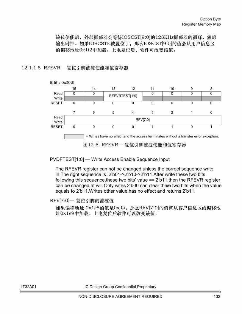
Option Byte Register Memory Map
该位使能后,外部振荡器会等待IOSCST[9:0]的128KHz振荡器的循环,然后输出时钟。如果IOSCSTE被置位了,那么IOSCST[9:0]的值会从用户信息区的偏移地址0x1f2中加载。上电复位后,软件可改变该值。
12.1.1.5 RFEVR— 复位引脚滤波使能和值寄存器
图12-5 RFEVR— 复位引脚滤波使能和值寄存器
PVDFTEST[1:0] — Write Access Enable Sequence Input
The RFEVR register can not be changed,unless the correct sequence write in.The right sequence is :2’b01->2’b10->2’b11.After write these two bits following this sequence,these two bits’ value == 2’b11,then the RFEVR register can be changed at will.Only writes 2’b00 can clear these two bits when the value equals to 2’b11.Writes other value has no effect and returns 2’b11.
RFV[7:0]— 复位引脚的滤波值如果偏移地址 0x1e8的值是0x9a,那么 RFV[7:0]的值就从客户信息区的偏移地址0x1e9中加载。上电复位后软件可以改变该值。
地址 : 0x0024 15 14 13 12 11 10 9 8
Read: 0 0RFEVRTEST[1:0]
0 0 0 0Write:
RESET: 0 0 0 0 0 0 0 0
7 6 5 4 3 2 1 0Read:
RFV[7:0]Write:
RESET: 0 0 0 0 1 1 0 1
= Writes have no effect and the access terminates without a transfer error exception.
LT32A01 IC Design Group Confidential Proprietary
NON-DISCLOSURE AGREEMENT REQUIRED 132

Option Byte Register Memory Map
12.1.1.6 PVDFEVR— 可编程电压检测器滤波器使能和值寄存器
图 12-6 PVDFEVR — 可编程电压检测器滤波器使能和值寄存器
PVDFTEST[1:0] — Write Access Enable Sequence Input
The PVDFEVR register can not be changed,unless the correct sequence write in.The right sequence is :2’b01->2’b10->2’b11.After write these two bits following this sequence,these two bits’ value == 2’b11,then the PVDFEVR register can be changed at will.Only writes 2’b00 can clear these two bits when the value equals to 2’b11.Writes other value has no effect and returns 2’b11.
PVDFE— 可编程的电压检测器滤波器使能PVDFE反映了上电后,可编程电压检测器滤波器的启动是否从用户信息区中加载。如果用户信息区的偏移地址0x1ea是0x7d,那么上电复位后,该可读/写位会被置位。否则上电复位后被清零。
1 = PVD 滤波器使能0 = PVD 滤波器禁止
PVDFV[7:0]— 可编程电压检测器滤波值如果PVDFE被置位,那么 PVDFV[7:0] 的值会从用户信息区的偏移地址0x1eb中加载。上电复位后,软件可改变该值。
地址: 0x002631 30 29 28 27 26 25 24
Read:PVDFE
0RVDFTEST[1:0]
0 0 0 0Write:
RESET: 0 0 0 0 0 0 0 0
23 22 21 20 19 18 17 16Read:
PVDFV[7:0]Write:
RESET: 0 0 0 0 0 0 0 0
= Writes have no effect and the access terminates without a transfer error exception.
LT32A01 IC Design Group Confidential Proprietary
NON-DISCLOSURE AGREEMENT REQUIRED 133

Option Byte Register Memory Map
12.1.1.7 FCR — 出厂配置寄存器
Note:1, Determined by flash trim
图 12-7 FCR — 出厂配置寄存器
FIAPPDIS— 出厂信息区程序禁用位FIAPPDIS反映了出厂信息区的程序是否被禁止。如果出厂信息区的偏移地址0x1ff 是0x82,那么上电复位后,该只读位会被置位。否则,该位被清零。
1 = 出厂信息区程序禁用0 = 出厂信息区程序使能
FIAPEDIS— 出厂信息区页擦除禁止位FIAPEDIS反映了如果出厂信息区的页擦除是否禁止。如果出厂信息区的偏移地址0x1fe是0xae,那么上电复位后,该只读位会被置位。否则,该位被清零。
1 = 出厂信息区页擦除禁止0 = 出厂信息区页擦除使能
TMDIS— 测试模式禁止位TTMDIS 反映了出来STB的测试模式是否被禁止。如果出厂信息区的偏移地址0x1fd是0x96,那么上电复位后,该只读位会被置位。否则,该位被清零。
1 = 测试模式禁止0 = 测试模式使能
IOSCTE — 内部高速振荡器调整使能
地址 : 0x002e31 30 29 28 27 26 25 24
Read: FIAPPDIS FIAPEDIS 0 TMDIS IOSCTE LDOTE VREFTE GLFTEWrite:
RESET: Note1 Note1 0 Note1 Note1 Note1 0 0
23 22 21 20 19 18 17 16
Read: MPUPDIS MPUEDIS 0 0 0 0 0 BIGENDI-AN
Write:RESET: 0 0 0 0 0 0 0 0
= Writes have no effect and the access terminates without a transfer error exception.
LT32A01 IC Design Group Confidential Proprietary
NON-DISCLOSURE AGREEMENT REQUIRED 134

Option Byte Register Memory Map
IOSCSTE显示了内部高速振荡器是否调整了。如果出厂信息区的地址偏移0x1f8是0xbd,那么上电复位后该只读位会被置位。否则,上电复位后被清零。
1 = 内部高速振荡器调整了0 = 内部高速振荡器没有调整
LDOTE — LDO调整使能LDOTE位显示了LDO是否调整了。如果出厂信息区的地址偏移0x1f4是0x854f,那么上电复位后该只读位会被置位。否则,上电复位后被清零。
1 = LDO调整了0 = LDO没有调整
VREFTE— VREF模块调整配置寄存器VREFTE位显示了VREF模块是否调整了,如果出厂信息区的0x1ec是0x5a,那么上电复位后该只读位会被置位。否则,上电复位后被清零。
1 = Internal VREF Module Trimming Configuration loaded from factory Information Area after POR
0 = Internal VREF Module Trimming Configuration not loaded from factory Information Area after POR
GLFTE— Glitch Filter Module Trimming Configuration RegisterThe GLFTE shows whether Glitch Filter Module is trimmed. If the offset adress 0x1ee of the factory information area is 0xad, the read only bit is set after power on reset. Otherwise, it is clear after power on reset.
1 = Glitch Filter Module Trimming Configuration loaded from factory Information Area after POR
0 = Glitch Filter Module Trimming Configuration not loaded from factory Information Area after POR
MPUPDIS— MPU配置信息区程序禁用位MPUPDIS反映了MPU配置信息区的程序是否被禁止。如果MPU配置信息区的偏移地址0x1ff是0xa5, 那么上电复位后,该只读位会被置位。否则,该位被清零。
1 = MPU 配置信息区编程禁止0 = MPU 配置信息区编程使能
MPUEDIS— MPU配置信息区也擦除禁止位
LT32A01 IC Design Group Confidential Proprietary
NON-DISCLOSURE AGREEMENT REQUIRED 135
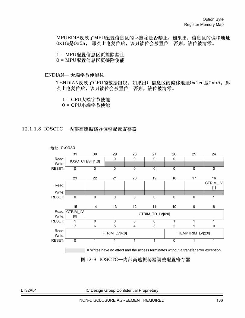
Option Byte Register Memory Map
MPUEDIS反映了MPU配置信息区的耶擦除是否禁止。如果出厂信息区的偏移地址0x1fe是0x5a, 那么上电复位后,该只读位会被置位。否则,该位被清零。
1 = MPU配置信息区页擦除禁止0 = MPU配置信息区页擦除使能
ENDIAN— 大端字节使能位TENDIAN反映了CPU的数据组织。如果出厂信息区的偏移地址0x1ea是0xb5,那么上电复位后,该只读位会被置位。否则,该位被清零。
1 = CPU大端字节使能0 = CPU小端字节使能
12.1.1.8 IOSCTC— 内部高速振荡器调整配置寄存器
图12-8 IOSCTC—内部高速振荡器调整配置寄存器
地址: 0x003031 30 29 28 27 26 25 24
Read:IOSCTCTEST[1:0]
0 0 0 0Write:
RESET: 0 0 0 0 0 0 0 0
23 22 21 20 19 18 17 16
Read: CTRIM_LV[1]
Write:RESET: 0 0 0 0 0 0 0 1
15 14 13 12 11 10 9 8Read: CTRIM_LV
[0] CTRIM_TD_LV[6:0]Write:
RESET: 1 0 0 0 0 1 1 17 6 5 4 3 2 1 0
Read:FTRIM_LV[4:0] TEMPTRIM_LV[2:0]
Write:RESET: 0 1 1 1 1 0 1 1
= Writes have no effect and the access terminates without a transfer error exception.
LT32A01 IC Design Group Confidential Proprietary
NON-DISCLOSURE AGREEMENT REQUIRED 136

Option Byte Register Memory Map
IOSCTCTEST[1:0] —IOSCTC Write Access Sequence InThe IOSCTC register can not be changed,unless the correct sequence write in.The right sequence is :2’b01->2’b10->2’b11.After write these two bits following this sequence,these two bits’ value == 2’b11,then the IOSCTC register can be changed at will.Only writes 2’b00 can clear these two bits when the value equals to 2’b11.Writes other value has no effect and returns 2’b11.
CTRIM_LV[1:0] — Coarse Trimming Value for high speed oscillator
CTRIM_TD_LV[4:0] — Coarse Trimming Value for high speed oscillator
FTRIM_LV[6:0] — Fine Trimming Value for high speed oscillator
TEMPTRIM_LV[2:0]— Temperature correction for high speed oscillator
12.1.1.9 ADCCDISR— ADC通道禁用配置寄存器
•
Figure 12-9 GLFTCR— Glitch Filter Trimming Configuration Register
ADCCDISTEST[1:0] — Write Access Enable Seqence Input
The ADCCDISTEST register can not be changed,unless the correct sequence write in.The right sequence is :2’b01->2’b10->2’b11.After write these two bits following this sequence,these two bits’ value == 2’b11,then the ADCCDISTEST register can be changed at will.Only writes 2’b00 can clear these two bits when the value equals to 2’b11.Writes other value has no effect and returns 2’b11.
ADCCDIS[7:3]— ADC通道禁用配置
地址: 0x003415 14 13 12 11 10 9 8
Read:ADCCDISTEST[1:0]
0Write:
RESET: 0 0 0 0 0 0 0 07 6 5 4 3 2 1 0
Read:ADCCDIS[7:3]
0Write:
RESET: 0 0 0 0 0 0 0 0= Writes have no effect and the access terminates without a transfer error exception.
LT32A01 IC Design Group Confidential Proprietary
NON-DISCLOSURE AGREEMENT REQUIRED 137

Option Byte Register Memory Map
在CCR寄存器里,如果ADCSPOR被置位了,那么,ADCCDIS[7:3]会从用户信息区(位[7:3])的偏移地址0x1db中加载值。上电复位后,软件可改变该位的值。如果相应的位被置位了,那么ADC通道被禁止,并且ADC将作为GPIO口。
12.1.1.10 VREFTCR— VREF调整配置寄存器
• Note:1, Determined by the value of Factory Information Area
图12-10 VREFTCR— VREF调整配置寄存器
VREFTCTEST[1:0] — WSFTCR Write Access Sequence InThe VREFTCTEST register can not be changed,unless the correct sequence write in.The right sequence is :2’b01->2’b10->2’b11.After write these two bits following this sequence,these two bits’ value == 2’b11,then the VREFTCTEST register can be changed at will.Only writes 2’b00 can clear these two bits when the value equals to 2’b11.Writes other value has no effect and returns 2’b11.
VREFTRIM[4:0] — VREF调整值If VREFTE in FCR is set, VREFTRIM[4:0] is the last 5 bit of the loaded Value from the offset adress 0x1ed of the factory information area. Software can change it after power on reset.
ADC通道 禁止
ADC通道使能
int0[3] ain[3]int0[4] ain[4]int0[5] ain[5]int0[6] ain[6]int0[7] ain[7]
地址: 0x0036 23 22 21 20 19 18 17 16
Read:VREFTCTEST[1:0]
0VREFTRIM[4:0]
Write:RESET: Note1 0 0 0 0 0 0 0
= Writes have no effect and the access terminates without a transfer error exception.
LT32A01 IC Design Group Confidential Proprietary
NON-DISCLOSURE AGREEMENT REQUIRED 138

Option Byte Register Memory Map
12.1.1.11 LDOTC— LDO调整配置寄存器
图12-11 LDOTC— LDO调整配置寄存器
LDOTEST[1:0] — LDOTC Write Access Sequence InThe LDOTC register can not be changed,unless the correct sequence write in.The right sequence is :2’b01->2’b10->2’b11.After write these two bits following this sequence,these two bits’ value == 2’b11,then the LDOTC register can be changed at will.Only writes 2’b00 can clear these two bits when the value equals to 2’b11.Writes other value has no effect and returns 2’b11.
VREFPD — Internal 1.2Voltage Reference Source Power Down1 = Internal Reference Voltage Source Power Down0 = Internal Reference Voltage Source Power On
LDOTC[3:0] — LDO调整值If LDOTE is set, LDOTC[3:0] is the last 4 bit of the loaded Value from the offset adress 0x1f7 of the factory information area. Software can change it after power on reset.
地址 : 0x0037 31 30 29 28 27 26 25 24
Read:LDOTEST[1:0] VREFPD
0LDOTC[3:0]
Write:RESET: 0 0 0 0 0 0 0 0
= Writes have no effect and the access terminates without a transfer error exception.
LT32A01 IC Design Group Confidential Proprietary
NON-DISCLOSURE AGREEMENT REQUIRED 139

Option Byte Register Memory Map
12.1.1.12 MPUCONFR— Memory Protect Unit Trimming Configuration Register
Figure 12-12 MPUCONFR—Memory Proect Unit Configuration Register
MPU_EN — MPU 使能状态位1 = MPU 使能0 = MPU 禁止
OVMPU — MPU配置区域覆盖状态位1 = MPU 配置被FIA MPU配置覆盖0 = MPU 配置不被FIA MPU配置覆盖
MPULREN — MPU area local read enabled status bit, default local or external read is disabled
1 = Memory protected area is readable by the local read0 = Memory protected area is not readable by the local read
MPU_H_PAGE_ADDR[6:0] — Memory protected area higher page boundary, and the protected area size is (MPU_H_PAGE_ADDR[6:0] - MPU_L_PAGE_ADDR[6:0]) * 512Bytes
Address : 0x0038 31 30 29 28 27 26 25 24
Read: MPU_EN OVMPU 0 0 0 0 0 0Write:
RESET: 0 0 0 0 0 0 0 0
23 22 21 20 19 18 17 16Read: 0 MPU_H_PAGE_ADDR[6:0]Write:
RESET: 0 0 0 0 0 0 0 1
15 14 13 12 11 10 9 8Read: MPULREN 0 0 0 0 0 0 0Write:
RESET: 0 0 0 0 0 0 0 07 6 5 4 3 2 1 0
Read: 0 MPU_L_PAGE_ADDR[6:0]Write:
RESET: 0 0 0 0 0 0 0 0
= Writes have no effect and the access terminates without a transfer error exception.
LT32A01 IC Design Group Confidential Proprietary
NON-DISCLOSURE AGREEMENT REQUIRED 140

Option Byte Register Memory Map
MPU_L_PAGE_ADDR[6:0] — Memory protected area lower page boundary, and the protected area size is (MPU_H_PAGE_ADDR[6:0] - MPU_L_PAGE_ADDR[6:0]) * 512Bytes
12.1.1.13 GLFTC— Glitch Filter Trimming Configuration Register
• Note:1, Determined by the value of Factory Information Area
Figure 12-13 GLFTCR— Glitch Filter Trimming Configuration Register
GLFTCTEST[1:0] — Write Access Enable Seqence Input
The GLFTCTEST register can not be changed,unless the correct sequence write in.The right sequence is :2’b01->2’b10->2’b11.After write these two bits following this sequence,these two bits’ value == 2’b11,then the GLFTCTEST register can be changed at will.Only writes 2’b00 can clear these two bits when the value equals to 2’b11.Writes other value has no effect and returns 2’b11.
50NSGLF_TRIM[3:0]— 50ns Glitch Filter Trimming ValueIf GLFTE is set, 50NSGLF_TRIM[3:0] are loaded Value from the offset adress 0x1ef of the factory information area(bit[7:4]). Software can change it after power on reset.
10NSGLF_TRIM[3:0]— 10ns Glitch Filter Trimming Value
If GLFTE is set, 10NSGLF_TRIM[3:0] are loaded Value from the offset adress 0x1ef of the factory information area(bit[3:0]). Software can change it after power on reset.
Address : 0x003e15 14 13 12 11 10 9 8
Read:GLFTCTEST[1:0]
0Write:
RESET: Note1 0 0 0 0 0 0 07 6 5 4 3 2 1 0
Read:10NSGLF_TRIM[3:0] 50NSGLF_TRIM[3:0]
Write:RESET: 1 0 0 0 0 1 1 0
= Writes have no effect and the access terminates without a transfer error exception.
LT32A01 IC Design Group Confidential Proprietary
NON-DISCLOSURE AGREEMENT REQUIRED 141

Advance Information — DMA
第十三节: LDMA控制器
13.1 介绍
LDMA控制器是通过请求确认,直接在存储器和外设之间传输数据的。LDMA模块提供三个通道,即允许字节、半字和字的传输。
13.2 特性
LDMA控制器的特性包括:
• 3个独立的可编程LDMA控制器通道
• 通道0到通道3的固定优先级
• 可编程存储器的基地址
• 可编程字节计数器
• 可编程字节配置
• 可编程传输大小
• 多个外设选择
• 支持硬件请求确认
13.3 低功率模式操作
LDMA控制器不受任何低功耗模式的影响。CPU可以通过在时钟模块里设置相应的模块停止位来停止LDMA。
DMA LT32A01
NON-DISCLOSURE AGREEMENT REQUIRED 142

LDMA Controller
I
13.4 框图
LDMAC可以从内存传输数据到外设,也可以从外设传输数据到内存。外设可以是SP和ADC等。 Memory. The peripheral can be SPI, ADC.
图 13-1 LDMAC框图
IPBUS
LDMAC Control Registers
LDMAC Status Register
LDMAC Process Controller
SRAM Peripheral
IC Design Group Confidential Proprietary DMA
143 NON-DISCLOSURE AGREEMENT REQUIRED

LDMA Controller Module Memory Map
LDMA M通道2的内存基地址寄存器(LDMAMBAR2)
13.5 模块内存映射
表 13-1 列出了LDMAC的寄存器模块内存映射。
表 13-1 R寄存器内存映射 地址 偏移 位 31-24 位23-16 位15-8 位 7-0 访问1,2
0x0000 LDMA 状态寄存器(LDMASR) S/U0x0004 LDMA 通道0的内存基地址寄存器(LDMAMBAR0) S/U0x0008 LDMA 通道0的字节计算寄存器(LDMABCR0) S/U0x000c LDMA 通道0的控制寄存器(LDMACR0) S/U0x0010 LDMA 通道1的内存基地址寄存器(LDMAMBAR1) S/U0x0014 LDMA 通道1的字节计算寄存器(LDMABCR1) S/U0x0018 LDMA 通道1的控制寄存器(LDMACR1) S/U0x001c S/U0x0020 LDMA 通道2的字节计算寄存器(LDMABCR2) S/U
NOTES:1. S = CPU supervisor mode access only.2. User mode accesses to supervisor-only address locations hav e no effect and result in a cycle termination transfer
error.
0x0024 LDMA 通道2的字节计算寄存器(LDMABCR2) S/U
DMA IC Design Group Confidential Proprietary
NON-DISCLOSURE AGREEMENT REQUIRED 144

LDMA Controller
13.6 寄存器描述
13.6.1 LDMA 状态寄存器 (LDMASR)
图13-2 LDMA 状态寄存器(LDMASR)
HTIFx — 通道x的半传输标志当传输了字节的一半时,该位被硬件置位。写1可以清除该位。
1 = 通道x传输了字节的一半0 = 通道x没有传输字节的一半
说明:当传输的字节达到BCRx/2时,HTIFx置位。PTSx也可以决定HTIFx是否置位When PTSx=’b00/’b11,BCRx>’b100,HTIFx is valid.
PTSx=’b10,BCRx>’b10,HTIFx is valid.
PTSx=’b01,BCRx>’b1,HTIFx is valid.
TCIFx — 通道x传输完成标志
当所有的字节传输完成时,该位被硬件置位。写1可以清除该位。
1 = 通道x传输完成
地址偏移 : 从0x0000 到0x000331 30 29 28 27 26 25 24
R 0 0 0 0 0 0 0 0W
RESET: 0 0 0 0 0 0 0 0
23 22 21 20 19 18 17 16R 0 0 0 0 0 0 0 0W
RESET: 0 0 0 0 0 0 0 0
15 14 13 12 11 10 9 8R 0 0 0 0 0 0 0 0W
RESET: 0 0 0 0 0 0 0 0
7 6 5 4 3 2 1 0R 0 0 HTIF2 TCIF2 HTIF1 TCIF1 HTIF0 TCIF0W
RESET: 0 0 0 0 0 0 0 0
= Writes have no effect and the access terminates without a transfer error exception.
IC Design Group Confidential Proprietary DMA
145 NON-DISCLOSURE AGREEMENT REQUIRED

LDMA Controller Register Descriptions
0 = 通道x传输未完成
13.6.2 LDMA 内存基地址寄存器 (LDMAMBARx)
在传输操作期间,MBARx会保持最初的编程值。MBARx不会从通道x的内存地址计数器中加载值,直到通道x开始传输。在循环模式中,最后一次传输结束后,MBARx胡自动地内存地址计数器中加载值。
图13-3 LDMA 通道x的内存基地址寄存器(LDMAMBARx)
地址偏移 : 0x0004+n*0xc,where n=0 to 231 30 29 28 27 26 25 24
R 0 0 0 0 0 0 0 0W
RESET: 0 0 0 0 0 0 0 0
23 22 21 20 19 18 17 16R 0 0 0 0 0 0 0 0W
RESET: 0 0 0 0 0 0 0 0
15 14 13 12 11 10 9 8R
MBARx[15:8]W
RESET: 0 0 0 0 0 0 0 0
7 6 5 4 3 2 1 0R
MBARx[7:2]0 0
WRESET: 0 0 0 0 0 0 0 0
= Writes have no effect and the access terminates without a transfer error exception.
DMA IC Design Group Confidential Proprietary
NON-DISCLOSURE AGREEMENT REQUIRED 146

LDMA Controller
13.6.3 LDMA字节计算寄存器 (LDMABCRx)
BCRx register bits contain the number of bytes yet to be transferred of channelx.When channelx transfer start,BCRx will be loaded into the internal byte counter. Internal byte counter decrements on the successful completion of a transfer and decrements by 1,2 or 4 for byte,half-word or word transfer respectively.BCRx signal the Internal byte counter value when channelx is transferring.
Once the channelx transfer complete, the internal byte counter can either stay at zero or reloaded with the BCRx value previous programmed automatically(in circular mode).
图 13-4 LDMA 通道x的字节计算寄存器 (LDMABCRx)
偏移地址: 0x0008+n*0xc,where n=0 to 231 30 29 28 27 26 25 24
R 0 0 0 0 0 0 0 0W
RESET: 0 0 0 0 0 0 0 0
23 22 21 20 19 18 17 16R 0] 0 0 0 0 0 0 0W
RESET: 0 0 0 0 0 0 0 0
15 14 13 12 11 10 9 8R
BCRx[15:8]W
RESET: 0 0 0 0 0 0 0 0
7 6 5 4 3 2 1 0R
BCRx[7:0]W
RESET: 0 0 0 0 0 0 0 0
= Writes have no effect and the access terminates without a transfer error exception.
27 Mar 2012 — Rev 0.4 IC Design Group Confidential Proprietary DMA
147 NON-DISCLOSURE AGREEMENT REQUIRED

LDMA Controller Register Descriptions
13.6.4 LDMA 控制寄存器 (LDMACRx)
图13-5 LDMA 通道x的控制寄存器(LDMACRx)
STARTx — 通道x的开始位STARTx 位指示了通道x是否有效。当清除STARTx 位后,通道x被禁止。
1 = 通道x有效0 = 通道x无效
说明:在置位 STARTx之前,请先配置 LDMACRx 的其他位。如要开始LDMA传输,把置位 STARTx放在最后。
LBFEx — 左边字节先传输使能1 = 左边字节先传输0 = 右边字节先传输
PTSx[1:0] — 外设传输大小
地址偏移 : 0x000c+n*0xc,where n=0 to 331 30 29 28 27 26 25 24
R BUSYx CEx 0 0 0 0 0 0W
RESET: 0 0 0 0 0 0 0 0
23 22 21 20 19 18 17 16R 0 0 0 0 0 0
HTIEx TCIExW
RESET: 0 0 0 0 0 0 0 0
15 14 13 12 11 10 9 8R 0 0 0 0 0
PSx[1:0] EHRxW
RESET: 0 0 0 0 0 0 0 0
7 6 5 4 3 2 1 0R
CIRCx MINCx MDECx TDx PTSx[1:0] LBFEx STARTxW
RESET: 0 0 0 0 0 0 0 0
= Writes have no effect and the access terminates without a transfer error exception.
表 13-2 外设传输大小PTS[1:0] 传输大小
00 字01 字节10 半字11 保留
DMA IC Design Group Confidential Proprietary 27 Mar 2012 — Rev 0.4
NON-DISCLOSURE AGREEMENT REQUIRED 148

LDMA Controller
TDx— 传输方向TDx 位决定了传输的方向。
1 = 传输方向为外设到内存0 = 传输方向为内存到外设
MINCx —内存地址增量
MDECx — 内存地址减量MINCx 和 MDECx 位决定了成功传输后的内存地址是增加还是减少。
CIRCx — 循环模式使能1 = 循环模式使能0 = 循环模式禁止
EHRx — 硬件触发模式使能
EHRx 位通过硬件触发器使能通道x。如果 EHRx=0,一旦通道开启了,它可以服务任何来自通道上的外设的DMA请求。 如果 EHRx=1,它不能服务来自外设的DMA请求,直到通道x发送硬件触发信号给LDMA。
1 = 硬件触发模式使能0 = 硬件触发模式禁止
表13-3 通道的硬件触发任务
PSx[1:0] — 外设选择PS[1:0] 位决定了哪个外设位被选择。
说明:PS[1:0] 应被设置为2’b00
Table 13-4 Peripheral assignment of the channels
MINCx MDECx Description0 0 内存地址没变化0 1 内存地址增加1 0 内存地址减少1 1 内存地址没变化
通道号 硬件触发0 PIT11 PIT22 PIT3
27 Mar 2012 — Rev 0.4 IC Design Group Confidential Proprietary DMA
149 NON-DISCLOSURE AGREEMENT REQUIRED

LDMA Controller Register Descriptions
。
TCIE — 传输完成中断使能位TCIE 位使能相应的LDMASR的TCIFx标志以产生中断请求。 1 = 相应的TCIF中断请求使能
0 = 相应的TCIF中断请求禁止
HTIE — Half Memory Reach Interrupt Enable BitThis HMRIE bit enable the corresponding channel HTIFx flag of LDMASR to generate interrupt request.
1 = The corresponding HTIF interrupt request enabled0 = The corresponding HTIF interrupt request disabled
CEx — 配置错误标志当发生配置错误时,CE位会被置位。当PTSx=2’b00 而且BCRx[1:0]!=2’b00时,CEx被置位。当 PTSx=2’b10并且BCRx[0]=1’b1时,CEx被置位。该位的置位是自动的。
1 = 发生配置错误0 = 未发生错误配置
说明:配置完LDMACRx后请检查CEx位,如果CEx=1,请重新正确配置LDMACRx
BUSYx — 通道x传输忙该指示了通道x是否传输忙。该位的置位和清零都是自动的。
1 = 通道x传输忙0 = 通道x空闲
通道号 PS[1:0] 外设
00 ADC 读
1~3 保留
10 SPI 写
1~3 保留
20 SPI 读
1~3 保留
DMA IC Design Group Confidential Proprietary 27 Mar 2012 — Rev 0.4
NON-DISCLOSURE AGREEMENT REQUIRED 150

LDMA Controller
13.7 功能描述
13.7.1 循环模式
Circular mode is available to handle circular buffers and continuous data flows (e.g. ADC scan mode). This feature can be enabled using the CIRC bit in the LDMACRx register. When circular mode is activated, the number of data to be transferred is automatically reloaded with the initial value programmed during the channel configuration phase, and the DMA requests continue to be served.
13.7.2 通道配置过程
配置LDMA的通道x(x为通道号)应该遵循以下顺序。
1. 设置LDMAMARx寄存器内的内存地址。外设事件之后,数据将写入内存或从内存中读取。
2. 配置LDMABCRx寄存器里要传输的数据总数。每个外设事件结束后,该值都会增加。
3. 配置LDMACRx寄存器,除了STARTx位。检查LDMACRx里的CEx位,如果CEx=1,请重新配置LDMACRx寄存器。
4. 通过设置LDMACRx寄存器里的STARTx位来激活通道x。
EHRx 位通过硬件触发器使能通道x。如果 EHRx=0,一旦通道开启了,它可以服务任何来自通道上的外设的DMA请求。 如果 EHRx=1,它不能服务来自外设的DMA请求,直到通道x发送硬件触发信号给LDMA。
Once half of the bytes are transferred, the half-transfer flag (HTIF) is set and an interrupt is generated if the Half-Transfer Interrupt Enable bit (HTIE) is set. In no-circular mode,at the end of the transfer, the Transfer Complete Flag (TCIF) is set and an interrupt is generated if the Transfer Complete Interrupt Enable bit (TCIE) is set.
27 Mar 2012 — Rev 0.4 IC Design Group Confidential Proprietary DMA
151 NON-DISCLOSURE AGREEMENT REQUIRED

Programmable Interrupt Timer Modules (PIT) Introduction
第十四节:可编程中断定时器模块(PIT)
14.1 介绍
可编程中断定时器(PIT)是一个16位的定时器,它提供了精确的中断处理器定期最小干预。定时器可以从锁存在模块里的数开始向下计数,也可以自由向下计数。
14.2 框图
图 14-1 PIT 框图
LT32A01 IC Design Group Confidential Proprietary 24 Jun 2013 — Rev 0.1
NON-DISCLOSURE AGREEMENT REQUIRED 152

Programmable Interrupt Timer Modules (PIT) Modes of Operation
14.3 操作模式
本小节介绍3个低功耗模式和调试模式。
14.3.1 等待模式
在等待模式中,PIT模块继续正常运行,并且可以通过配置产生一个中断请求来退出低功耗模式。
14.3.2 休眠模式
若PIT控制与状态寄存器(PCSR)里的PDOZE位被置位了,那么PIT模块的操作将停止。如果PDOZE位被清零了,休眠模式不会对PIT的操作产生影响。当退出休眠模式时,PIT模块的操作将从进入休眠模式前的状态继续进行。
14.3.3 停止模式
在停止模式下,系统时钟不被激活,PIT模块停止操作。
14.3.4 调试模式
在调试模式下,PCSR寄存器中的PDBG位被置位后,PIT模块的操作会停止。若PDBG位被清零,调试模式不会影响到PIT模块的操作。当退出调试模式时,PIT会从进入调试模式之前的状态继续操作,但任何的在调试模式内的更新都会保持。
14.4 信号
The PIT module has no off-chip signals.
14.5 内存映射和寄存器
本小节介绍了PIT的内存映射和寄存器结构。
LT32A01 IC Design Group Confidential Proprietary 24 Jun 2013 — Rev 0.1
NON-DISCLOSURE AGREEMENT REQUIRED 153
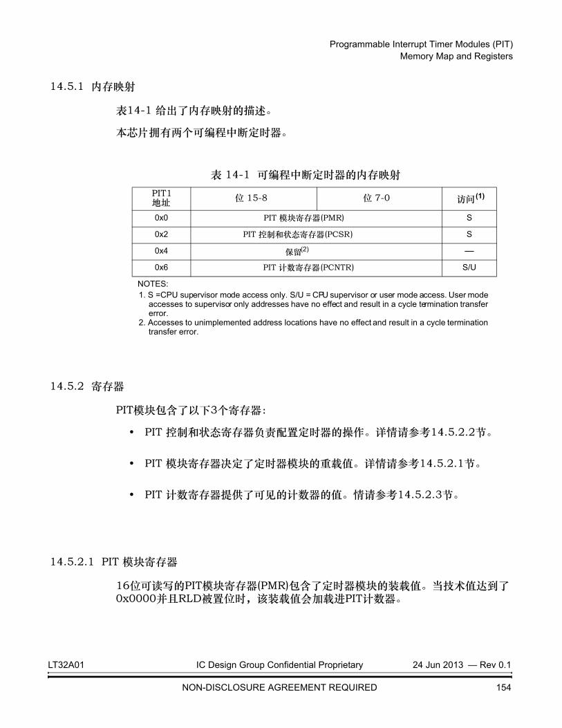
Programmable Interrupt Timer Modules (PIT) Memory Map and Registers
14.5.1 内存映射
表14-1 给出了内存映射的描述。
本芯片拥有两个可编程中断定时器。
14.5.2 寄存器
PIT模块包含了以下3个寄存器:
• PIT 控制和状态寄存器负责配置定时器的操作。详情请参考14.5.2.2节。
• PIT 模块寄存器决定了定时器模块的重载值。详情请参考14.5.2.1节。
• PIT 计数寄存器提供了可见的计数器的值。情请参考14.5.2.3节。
14.5.2.1 PIT 模块寄存器
16位可读写的PIT模块寄存器(PMR)包含了定时器模块的装载值。当技术值达到了0x0000并且RLD被置位时,该装载值会加载进PIT计数器。
表 14-1 可编程中断定时器的内存映射PIT1
地址 位 15-8 位 7-0 访问(1)
NOTES:1. S = CPU supervisor mode access only. S/U = CPU supervisor or user mode access. User mode
accesses to supervisor only addresses have no effect and result in a cycle termination transfer error.
0x0 PIT 模块寄存器 (PMR) S
0x2 PIT 控制和状态寄存器 (PCSR) S
0x4 保留(2)
2. Accesses to unimplemented address locations have no effect and result in a cycle termination transfer error.
—
0x6 PIT 计数寄存器 (PCNTR) S/U
LT32A01 IC Design Group Confidential Proprietary 24 Jun 2013 — Rev 0.1
NON-DISCLOSURE AGREEMENT REQUIRED 154

Programmable Interrupt Timer Modules (PIT) Memory Map and Registers
When the OVW bit is set, PMR is transparent, and the value written to PMR is immediately loaded into the PIT counter. The prescaler counter is reset anytime a new value is loaded into the PIT counter and also during reset. Reading the PMR returns the value written in the modulus latch. Reset initializes PMR to 0xFFFF.
图14-2 PIT 模块寄存器 (PMR)
14.5.2.2 PIT 控制和状态寄存器
图 14-3 PIT 控制和状态寄存器(PCSR)
PRE[3:0] — 预分频位该可读写PRE[3:0]位负责选择系统时钟的分频因子,以产生PIT时钟。详情请参考表14-2。为了准确预测下一个定时器计数值,只有在EN位被清零的时候才能改变PRE[3:0]位。PRE[3:0]的值被改变,预分频计数器会复位。系统复位以及装载新的计数值给计数器都会复位预分频计数器。置位EN位和往PRE[3:0]里写数据可以在同一个周期里完成。清除EN位可以调整预分频计数器的操作。
地址 : 0x000015 14 13 12 11 10 9 8
RPM15 PM14 PM13 PM12 PM11 PM10 PM9 PM8
WRESET: 1 1 1 1 1 1 1 1
7 6 5 4 3 2 1 0R
PM7 PM6 PM5 PM4 PM3 PM2 PM1 PM0W
RESET: 1 1 1 1 1 1 1 1
地址: 0x000215 14 13 12 11 10 9 8
R 0 0 0 0PRE3 PRE2 PRE1 PRE0
WRESET: 0 0 0 0 0 0 0 0
7 6 5 4 3 2 1 0R 0
PDOZE PDBG OVW PIE PIF RLD ENW
RESET: 0 0 0 0 0 0 0 0
= Writes have no effect and the access terminates without a transfer error exception.
LT32A01 IC Design Group Confidential Proprietary 24 Jun 2013 — Rev 0.1
NON-DISCLOSURE AGREEMENT REQUIRED 155
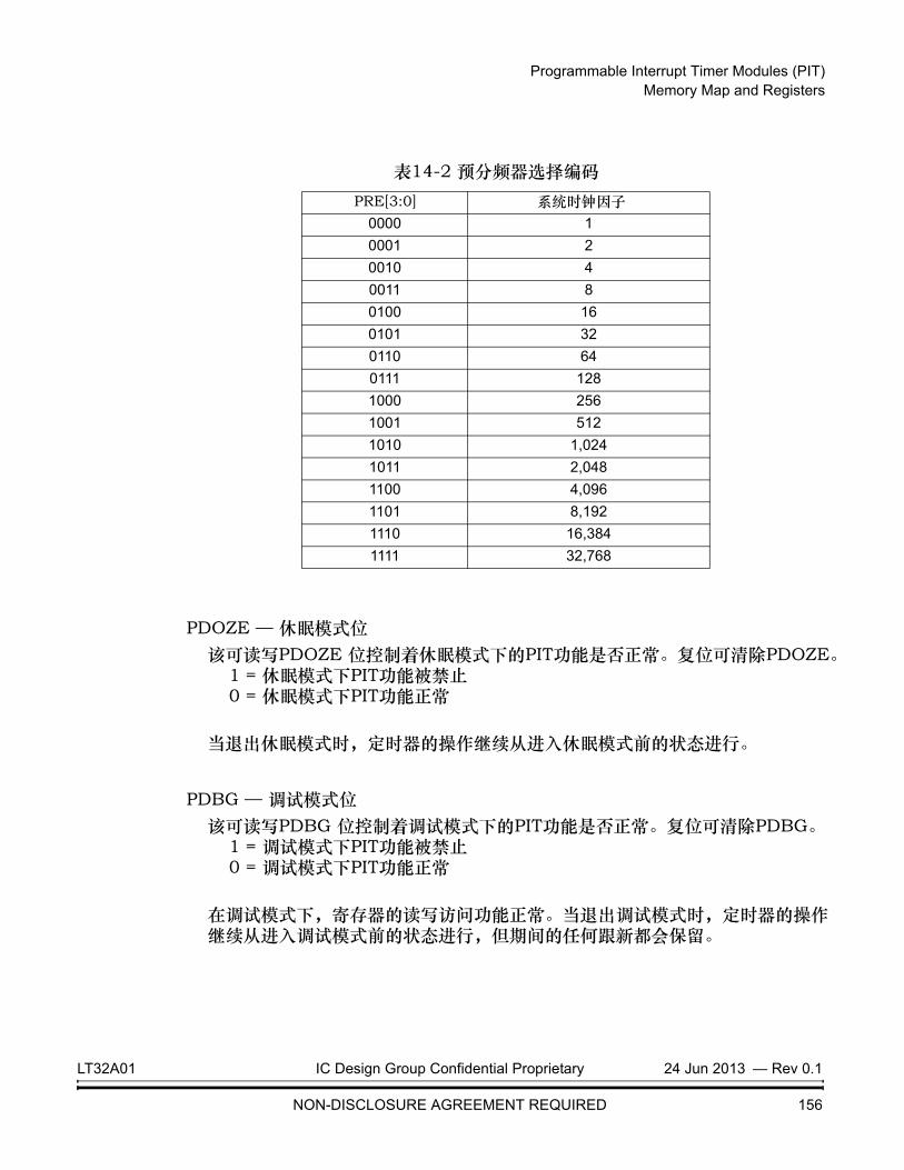
Programmable Interrupt Timer Modules (PIT) Memory Map and Registers
PDOZE — 休眠模式位该可读写PDOZE 位控制着休眠模式下的PIT功能是否正常。复位可清除PDOZE。
1 = 休眠模式下PIT功能被禁止0 = 休眠模式下PIT功能正常
当退出休眠模式时,定时器的操作继续从进入休眠模式前的状态进行。
PDBG — 调试模式位该可读写PDBG 位控制着调试模式下的PIT功能是否正常。复位可清除PDBG。
1 = 调试模式下PIT功能被禁止0 = 调试模式下PIT功能正常
在调试模式下,寄存器的读写访问功能正常。当退出调试模式时,定时器的操作继续从进入调试模式前的状态进行,但期间的任何跟新都会保留。
表14-2 预分频器选择编码PRE[3:0] 系统时钟因子
0000 10001 20010 40011 80100 160101 320110 640111 1281000 2561001 5121010 1,0241011 2,0481100 4,0961101 8,1921110 16,3841111 32,768
LT32A01 IC Design Group Confidential Proprietary 24 Jun 2013 — Rev 0.1
NON-DISCLOSURE AGREEMENT REQUIRED 156

Programmable Interrupt Timer Modules (PIT) Memory Map and Registers
说明: 在调试模式下,PDBG 位的值从1变化到0时,将启动PIT定时器。同样地,PDBG位的值从0变化到1时,将停止PIT定时器。
OVW — 覆盖位该可读写OVW 位允许写入PMR的值立刻覆盖PIT计数器的值。
1 = 写入PMR的值立刻替换PIT计数器的值0 = 当计数器的值达到0x0000,PMR的值替换PIT计数器的值
PIE — PIT 中断使能位该可读写PIE位使能PIF标志以产生中断请求。
1 = PIF 中断请求使能0 = PIF 中断请求禁止
PIF — PIT 中断标志当PIT计数器的计数值达到0x0000时,该可读写位被置位。通过写1或往PMR写入数据可以清除该位。写0没有影响。复位可以清除该位。
1 = PIT 计数值已达到 0x0000.0 = PIT 计数值还未达到0x0000.
RLD — 重装位当计数值达到0x0000时,该可读写位允许PMR的值装载进PIT计数器内。 1 = 计数值达到0x0000时,计数器重装PMR的值 0 = 计数值达到0x0000时,计数器重装0xFFFF
EN — PIT 使能位该位使能PT的操作。当PIT被禁止时,计数器和预分频器都处于停止状态。
1 = PIT 使能0 = PIT 禁止
14.5.2.3 PIT 计数寄存器
The 16-bit, read-only PIT Control Register (PCNTR) contains the counter value. Reading the 16-bit counter with two 8-bit reads is not guaranteed to be coherent. Writing to PCNTR has no effect, and write cycles are terminated normally.
LT32A01 IC Design Group Confidential Proprietary 24 Jun 2013 — Rev 0.1
NON-DISCLOSURE AGREEMENT REQUIRED 157

Programmable Interrupt Timer Modules (PIT) Functional Descripiton
图14-4 PIT 计数寄存器 (PCNTR)
14.6 功能描述
本小节介绍了PIT功能操作。
14.6.1 设置和遗忘定时器操作
当PCSR寄存器里的RLD位被置位了,该操作模式就会开启。
当PIT计数器的计数值达到0x0000时,PCSR寄存器的PIF标志位被置位。模块锁存器的值会加载进计数器内,并且计数器开始递减至0x0000。如果PCSR寄存器的PIE位被置位,PIF标志位会向CPU发出中断请求。
当PCSR寄存器的OVW位被置位了,通过往PMR里写入数据可以使计数器直接初始化,而不需要等到计数值达到0x0000。
地址 : 0x000615 14 13 12 11 10 9 8
R PC15 PC14 PC13 PC12 PC11 PC10 PC9 PC8W
RESET: 1 1 1 1 1 1 1 1
7 6 5 4 3 2 1 0R PC7 PC6 PC5 PC4 PC3 PC2 PC1 PC0W
RESET: 1 1 1 1 1 1 1 1
= Writes have no effect and the access terminates without a transfer error exception.
LT32A01 IC Design Group Confidential Proprietary 24 Jun 2013 — Rev 0.1
NON-DISCLOSURE AGREEMENT REQUIRED 158
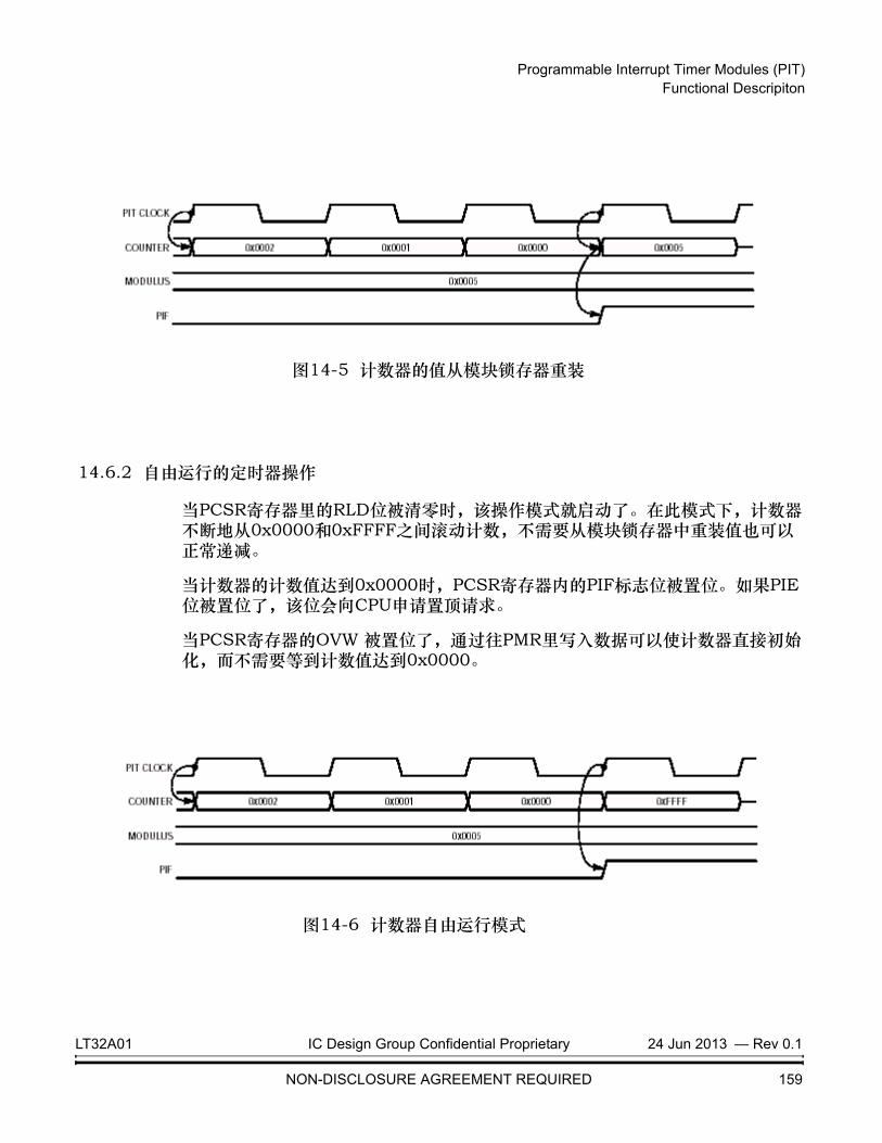
Programmable Interrupt Timer Modules (PIT) Functional Descripiton
图14-5 计数器的值从模块锁存器重装
14.6.2 自由运行的定时器操作
当PCSR寄存器里的RLD位被清零时,该操作模式就启动了。在此模式下,计数器不断地从0x0000和0xFFFF之间滚动计数,不需要从模块锁存器中重装值也可以正常递减。
当计数器的计数值达到0x0000时,PCSR寄存器内的PIF标志位被置位。如果PIE位被置位了,该位会向CPU申请置顶请求。
当PCSR寄存器的OVW 被置位了,通过往PMR里写入数据可以使计数器直接初始化,而不需要等到计数值达到0x0000。
图14-6 计数器自由运行模式
LT32A01 IC Design Group Confidential Proprietary 24 Jun 2013 — Rev 0.1
NON-DISCLOSURE AGREEMENT REQUIRED 159

Programmable Interrupt Timer Modules (PIT) Interrupt Operation
14.6.3 超时的规格
16位计数器和分频器支持不同的超时时间。通过设置PCSR寄存器内的PRE[3:0]使分频器分频系统时钟。PMR寄存器内的PM[15:0]可选择超时时间。
14.7 中断模式
表 14-3 列出了由PIT产生的中断请求。
当PIT计数器的计数值达到0x0000时,PIF标志位被置位。PIE位允许PIF标志位产生中断请求。通过写1或往PMR写入数据可以清除PIF标志位。
timeout period PRE 3:0[ ] PM 15:0[ ] 1+( ) clocks×=
表 14-3 PIT 中断请求s 中断请求 标志位 使能位
超时 PIF PIE
LT32A01 IC Design Group Confidential Proprietary 24 Jun 2013 — Rev 0.1
NON-DISCLOSURE AGREEMENT REQUIRED 160

Watchdog Timer Module Introduction
第十五节:看门狗定时器模块
15.1 介绍
看门狗定时器是一个16位的定时器,用于帮助软件从失控的代码中恢复,或者当操作的时间比预期的要长时,产生中断。看门狗定时器拥有一个自由运行计数器(看门狗计数器),可以产生一个复位或下溢中断。为了防止复位,软件必须周期性地通过服务看门狗重启倒数。
15.2 操作模式
本小节描述了在低功耗模式调试操作模式下的看门狗定时器的操作。
15.2.1 等待模式
看门狗控制寄存器(WCR)内的WAIT位被置位后即进入等待模式,看门狗定时器操作停止。 WAIT位被清零后,看门狗定时器继续正常运行。
15.2.2 休眠模式
看门狗控制寄存器(WCR)内的DOZE位被置位后即进入休眠模式,看门狗定时器操作停止。 DOZE位被清零后,看门狗定时器继续正常运行。
15.2.3 停止模式
看门狗控制寄存器(WCR)内的STOP位被置位后即进入停止模式,在停止模式下的看门狗操作停止。当退出停止模式时,看门狗操作继续从进入停止模式前的状态进行操作。 STOP位被清零后,看门狗定时器继续正常运行。
LT32A01 IC Design Group Confidential Proprietary 24 Jun 2013 — Rev 0.1
NON-DISCLOSURE AGREEMENT REQUIRED 161

Watchdog Timer Module Block Diagram
15.2.4 调试模式
WCR寄存器内的DBG位被置位后即进入调试模式,看门狗定时器模块停止操作。DBG位被清零后,看门狗定时器继续正常运作。 当退出调试模式时,门狗操作继续从进入调试模式前的状态进行操作,但其间的任何更新都会保留。
15.3 框图
图 15-1 看门狗定时器框图
IPBUS
16-BITS WCNTR 16-BITS WSR
16-BITS WATCHDOG COUNTER
IPBUS
16-BITS WMR
interruptresetDIVIDE
WDPEn
WaitDozestopDbg
32K CLK
LT32A01 IC Design Group Confidential Proprietary 24 Jun 2013 — Rev 0.1
NON-DISCLOSURE AGREEMENT REQUIRED 162

Watchdog Timer Module Signals
15.4 信号
The watchdog timer module has no off-chip signals.
15.5 内存映射与寄存器
本小节介绍了看门狗定时器的内存映射和寄存器。
15.5.1 内存映射
表15-1 给出了看门狗的内存映射描述。
15.5.2 寄存器
看门狗定时器的编程模型是包括以下寄存器:
• 看门狗控制寄存器(WCR)配置看门狗定时器的操作。详情请参考15.5.2.2看 门狗控制寄存器。• 看门狗模块寄存器(WMR)决定了定时器模块的重载值。详情请参考15.5.2.1 看门狗模块寄存器。.• 看门狗计数寄存器(WCNTR)提供了可视化的看门狗计数器的值。详情请
参考15.5.2.4看门狗计数寄存器。
表15-1 看门狗定时器模块内存映射
偏移地址 位15-8 位 7-0 访问权(1)
NOTES:
1. S = CPU supervisor mode access only. S/U = CPU supervisor or user mode access. User mode accesses to supervisor only addresses have no effect and result in a cycle termination transfer error.
0x0000 看门狗模块寄存器 (WMR) S
0x0002 看门狗控制寄存器 (WCR) S
0x0004 看门狗服务寄存器 (WSR) S/U
0x0006 看门狗计数寄存器(WCNTR) S/U
LT32A01 IC Design Group Confidential Proprietary 24 Jun 2013 — Rev 0.1
NON-DISCLOSURE AGREEMENT REQUIRED 163

Watchdog Timer Module Memory Map and Registers
• The Watchdog Service Register (WSR) requires a service sequence to prevent reset. See The read-only WC[15:0] field reflects the current value in the watchdog counter. Reading the 16-bit WCNTR with two 8-bit reads is not guaranteed to return a coherent value. Writing to WCNTR has no effect, and write cycles are terminated normally. This register is for watchdog work domain, so the read value maybe not stabilization, please read it time after time continuously..
LT32A01 IC Design Group Confidential Proprietary 24 Jun 2013 — Rev 0.1
NON-DISCLOSURE AGREEMENT REQUIRED 164
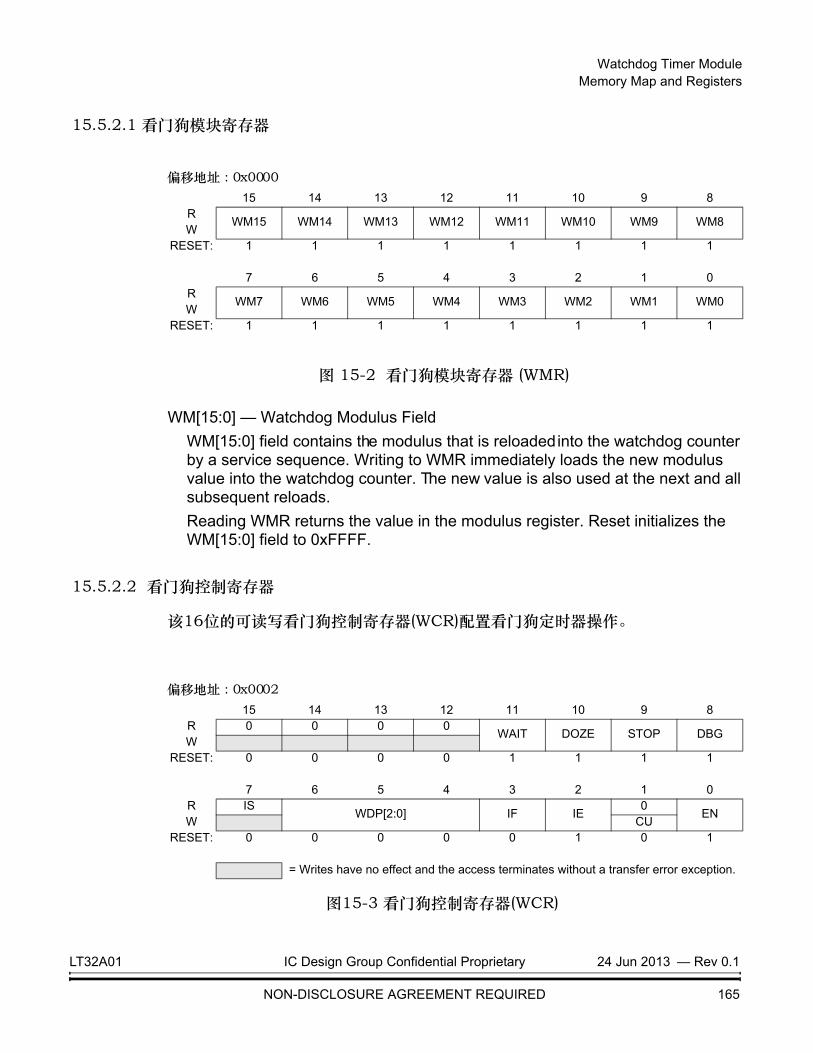
Watchdog Timer Module Memory Map and Registers
偏移地址 : 0x0002
偏移地址 : 0x0000
15.5.2.1 看门狗模块寄存器
图 15-2 看门狗模块寄存器 (WMR)
WM[15:0] — Watchdog Modulus FieldWM[15:0] field contains the modulus that is reloaded into the watchdog counter by a service sequence. Writing to WMR immediately loads the new modulus value into the watchdog counter. The new value is also used at the next and all subsequent reloads. Reading WMR returns the value in the modulus register. Reset initializes the WM[15:0] field to 0xFFFF.
15.5.2.2 看门狗控制寄存器
该16位的可读写看门狗控制寄存器(WCR)配置看门狗定时器操作。
图15-3 看门狗控制寄存器(WCR)
15 14 13 12 11 10 9 8R
WM15 WM14 WM13 WM12 WM11 WM10 WM9 WM8W
RESET: 1 1 1 1 1 1 1 1
7 6 5 4 3 2 1 0R
WM7 WM6 WM5 WM4 WM3 WM2 WM1 WM0W
RESET: 1 1 1 1 1 1 1 1
15 14 13 12 11 10 9 8R 0 0 0 0
WAIT DOZE STOP DBGW
RESET: 0 0 0 0 1 1 1 1
7 6 5 4 3 2 1 0R IS
WDP[2:0] IF IE0
ENW CU
RESET: 0 0 0 0 0 1 0 1
= Writes have no effect and the access terminates without a transfer error exception.
LT32A01 IC Design Group Confidential Proprietary 24 Jun 2013 — Rev 0.1
NON-DISCLOSURE AGREEMENT REQUIRED 165

Watchdog Timer Module Memory Map and Registers
WAIT — 等待模式位WAIT 位控制着等待模块下的看门狗定时器功能。
1 = 等待模式下,看门狗定时器停止0 = 等待模式下,看门狗定时器无影响
DOZE — 休眠模式位DOZE 位控制着休眠模式下的看门狗定时器功能。
1 = 休眠模式下,看门狗定时器停止0 = 休眠模式下,看门狗定时器无影响
STOP — 停止模式位STOP 位控制着停止模式下的看门狗定时器功能 。
1 = 休眠模式下,看门狗定时器停止0 = 休眠模式下,看门狗定时器无影响
DBG — 调试模式位DBG 控制着调试模式下的看门狗定时器功能。在调试模式期间,看门狗定时器寄存器可以正常地写入和读取正。当退出调试模式时,定时器继续从进入调试模式前的状态进行操作,但期间的任何更新都会保留。
1 = 调试模式下,看门狗定时器停止0 = 调试模式下,看门狗定时器无影响
说明: 在调试模式期间,DBG位从1变化到0即开启看门狗定时器。 在调试模式期间,DBG位从0变化到1即停止看门狗定时器。
EN — 看门狗使能位EN 位使能看门狗定时器。
1 = 看门狗定时器使能0 = 看门狗定时器禁止
CU — Watchdog Change Update BitWrite One to CU bit update the WDP[2:0] and WMR to the work latch.
IE — 看门狗中断使能位IE 位使能看门狗定时器中断模式。一旦中断产生,并且EN位是1,那么该位会被自动清零。
1 = 看门狗定时器中断模式使能0 = 看门狗定时器中断模式禁止
LT32A01 IC Design Group Confidential Proprietary 24 Jun 2013 — Rev 0.1
NON-DISCLOSURE AGREEMENT REQUIRED 166
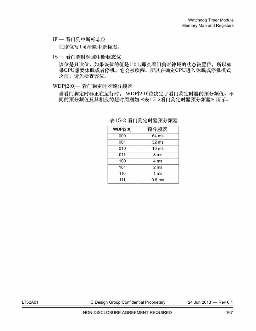
Watchdog Timer Module Memory Map and Registers
IF — 看门狗中断标志位往该位写1可清除中断标志。
IS — 看门狗时钟域中断状态位该位是只读位,如果该位的值是1'b1,那么看门狗时钟域的状态被置位,所以如果CPU想要休眠或者停机,它会被唤醒。所以在确定CPU进入休眠或停机模式之前,请先检查该位。
WDP[2:0] — 看门狗定时器预分频器当看门狗定时器正在运行时, WDP[2:0]位决定了看门狗定时器的预分频值。不同的预分频值及其相应的超时周期如《表15-2看门狗定时器预分频器》所示。
表15-2 看门狗定时器预分频器
WDP[2:0] 预分频器000 64 ms001 32 ms010 16 ms011 8 ms100 4 ms101 2 ms110 1 ms111 0.5 ms
LT32A01 IC Design Group Confidential Proprietary 24 Jun 2013 — Rev 0.1
NON-DISCLOSURE AGREEMENT REQUIRED 167

Watchdog Timer Module Memory Map and Registers
15.5.2.3 看门狗服务寄存器
当启动了看门狗定时器,要在看门狗计数器超时之前先看门狗服务寄存器(WSR)写0x5555,再写0xAAAA以防止复位。如果在超时之前WSR没有进行服务,那么看门狗定时器就会发生一个信号给复位控制器或者自动控制器,并且产生一个系统复位或中断。
Both writes must occur in the order listed before the timeout, but any number of instructions can be executed between the two writes. However, writing any value other than 0x5555 or 0xAAAA to WSR resets the servicing sequence, requiring both values to be written to keep the watchdog timer from causing a reset.
图15-4 看门狗复位寄存器
偏移地址: 0x000415 14 13 12 11 10 9 8
RWS15 WS14 WS13 WS12 WS11 WS10 WS9 WS8
WRESET: 0 0 0 0 0 0 0 0
7 6 5 4 3 2 1 0R
WS7 WS6 WS5 WS4 WS3 WS2 WS1 WS0W
RESET: 0 0 0 0 0 0 0 0
LT32A01 IC Design Group Confidential Proprietary 24 Jun 2013 — Rev 0.1
NON-DISCLOSURE AGREEMENT REQUIRED 168

Watchdog Timer Module Memory Map and Registers
15.5.2.4 看门狗计数寄存器
图 15-5 看门狗计数寄存器(WCNTR)
WC[15:0] — Watchdog Count FieldThe read-only WC[15:0] field reflects the current value in the watchdog counter. Reading the 16-bit WCNTR with two 8-bit reads is not guaranteed to return a coherent value. Writing to WCNTR has no effect, and write cycles are terminated normally. This register is for watchdog work domain, so the read value maybe not stabilization, please read it time after time continuously.
偏移地址 : 0x000615 14 13 12 11 10 9 8
R WC15 WC14 WC13 WC12 WC11 WC10 WC9 WC8W
RESET: 1 1 1 1 1 1 1 1
7 6 5 4 3 2 1 0R WC7 WC6 WC5 WC4 WC3 WC2 WC1 WC0W
RESET: 1 1 1 1 1 1 1 1
= Writes have no effect and the access terminates without a transfer error exception.
LT32A01 IC Design Group Confidential Proprietary 24 Jun 2013 — Rev 0.1
NON-DISCLOSURE AGREEMENT REQUIRED 169

Advance Information — EPORT
第十六节:边缘端口模块 (EPORT)
16.1 介绍
边缘端口模块(出口)有八个外部中断引脚。每个引脚可单独配置为低电平敏感的中断引脚,边沿检测中断引脚(上升沿,下降沿,或者两者都有),或一个通用输入/输出(I/O)引脚。详情见图16-1.
图 16-1 EPORT 框图
EPFC[n]
EPORT IC Design Group Confidential Proprietary Rev 0.4 — 27 Mar 2012
NON-DISCLOSURE AGREEMENT REQUIRED 170
Edge Port Module (EPORT) Low-Power Mode Operation
16.2 低功耗模式操作
本小节介绍了在低功耗模式下的EPORT模块的操作。
16.2.1 等待与休眠模式
在等待与休眠模式下。EPORT模块仍可以正常运行。可以通过配置外部引脚以产生边缘中断(上升沿或下降沿)请求或低电平中断请求来退出低功耗模式。
16.2.2 停止模式
在停止模式下,没有可用的时钟来执行边缘检测功能。只有电平检测逻辑是可用的,因此外部中断引脚上的任何低电平都可以产生一个中断,以此退出停止模式。
NOTE: The input pin synchronizer is bypassed for the level-detect logic since no clocks are available.
16.3 中断/通用I/O引脚说明
All pins default to general-purpose input pins at reset. The pin value is synchronized to the rising edge of CLKOUT when read from the EPORT Pin Data Register (EPPDR). The values used in the edge/level detect logic are also synchronized to the rising edge of CLKOUT. These pins use Schmitt triggered input buffers which have built in hysteresis designed to decrease the probability of generating false edge-triggered interrupts for slow rising and falling input signals.
16.4 内存映射与寄存器
本小节描述了内存映射和寄存器结构。
EPORT IC Design Group Confidential Proprietary 27 Mar 2012 — Rev 0.4
NON-DISCLOSURE AGREEMENT REQUIRED 171

Edge Port Module (EPORT) Memory Map and Registers
16.4.1 内存映射
表 16-1 列出了EPORT的内存映射。
16.4.2 寄存器
EPORT模块包含以下几个寄存器:
• EPORT 引脚分配寄存器 (EPPAR) 独立控制每个引脚的功能。
• EPORT 数据方向寄存器(EPDDR) 独立控制每个引脚的数据方向。
• EPORT 中断使能寄存器(EPIER) 独立地使能每个引脚中断请求。
• EPORT 数据寄存器(EPDR) 保持被驱动到引脚的数据。
• EPORT 引脚数据寄存器 (EPPDR) 反映引脚的当前状态。
• EPORT 标志寄存器(EPFR) 单独锁存EPORT边缘事件。
• EPORT 引脚上拉使能寄存器 (EPPUE) 单独控制每个引脚的上拉。
表 16-1 模块内存映射
地址偏移 位 15-8 位 7-0 访问权(1)
0x0000 EPORT 数据方向寄存器 (EPDDR) EPORT 中断使能寄存器 (EPIER) S
0x0002 EPORT 引脚分配寄存器(EPPAR) S
0x0004 EPORT 标志寄存器 (EPFR) EPORT 引脚上拉使能寄存器(EPPUE) S/U
0x0006 EPORT 数据寄存器 (EPDR) EPORT 引脚数据寄存器 (EPPDR) S/U
0x0008 EPORT 数字滤波控制寄存器(EPFC) EPORT 位设置寄存器 (EPBSR) S
0x000a EPORT 水平极性寄存器 (EPLPR) EPORT 开漏寄存器 (EPODE) S
0x000c 保留 S
0x000e EPORT 位清零寄存器 (EPBCR) S
NOTES:1. S = CPU supervisor mode access only. S/U = CPU supervisor or user mode access. User mode accesses to supervisor
only addresses have no effect and result in a cycle termination transfer error.
EPORT IC Design Group Confidential Proprietary 27 Mar 2012 — Rev 0.4
NON-DISCLOSURE AGREEMENT REQUIRED 172

Edge Port Module (EPORT) Memory Map and Registers
• EPORT 电平极性寄存器(EPLPR) 控制每个电平敏感引脚的电平极性。
• EPORT 开漏使能寄存器 (EPODE)单独控制每个引脚的输出开漏。
• EPORT 数字滤波控制寄存器(EPFC) 使能滤波器,并且控制被滤波的输入脉冲的宽度。
16.4.2.1 EPORT 中断使能寄存器
图 16-2 EPORT端口中断使能寄存器(EPIER)
EPIE[7:0] — EPORT中断使能位该可读写位使能 EPORT的中断请求。如果该位被置位了,当发生以下两种情况时,EPORT 将产生中断请求:
• The corresponding bit in the EPORT Flag Register (EPFR) is set or later becomes set, or
• 相应的引脚电平是低,并且引脚被配置为低电平敏感操作。
清除该位会否定来自相应EPORT引脚的任何中断请求。复位可清除EPIE[7:0]。1 = 相应EPORT引脚的中断请求使能0 = 想应EPORT引脚的中断请求禁止
地址偏移 : 0x00007 6 5 4 3 2 1 0
REPIE7 EPIE6 EPIE5 EPIE4 EPIE3 EPIE2 EPIE1 EPIE0
WRESET: 0 0 0 0 0 0 0 0
EPORT IC Design Group Confidential Proprietary 27 Mar 2012 — Rev 0.4
NON-DISCLOSURE AGREEMENT REQUIRED 173

Edge Port Module (EPORT) Memory Map and Registers
16.4.2.2 EPORT 数据方向寄存器
图 16-3 EPORT数据方向寄存器 (EPDDR)
EPDD[7:0] — EPORT 数据方向位置位EPDDR内的任何位都会配置相应位的管脚为输出。清除EPDDR内的任何位都会配置相应位的管脚为输入。 Pin direction is independent of the level/edge detection configuration.复位可清除EPDD[7:0].
To use an EPORT pin as an external interrupt request source, its corresponding bit in EPDDR must be clear. Software can generate interrupt requests by programming the EPORT Data Register when the EPDDR selects output.
1 = 相应的EPORT引脚配置为输出0 = 相应的EPORT引脚配置为输入
16.4.2.3 EPORT 引脚分配寄存器
图 16-4 EPORT引脚分配寄存器(EPPAR)
EPPA[7:0] — EPORT Pin Assignment Select FieldsThe read/write EPPAx fields configure EPORT pins for level detection and rising and/or falling edge detection as shows.
地址偏移 : 0x00017 6 5 4 3 2 1 0
REPDD7 EPDD6 EPDD5 EPDD4 EPDD3 EPDD2 EPDD1 EPDD0
WRESET: 0 0 0 0 0 0 0 0
地址偏移 : 0x0002 到 0x000315 14 13 12 11 10 9 8
REPPA7 EPPA6 EPPA5 EPPA4
WRESET: 0 0 0 0 0 0 0 0
7 6 5 4 3 2 1 0R
EPPA3 EPPA2 EPPA1 EPPA0W
RESET: 0 0 0 0 0 0 0 0
EPORT IC Design Group Confidential Proprietary 27 Mar 2012 — Rev 0.4
NON-DISCLOSURE AGREEMENT REQUIRED 174
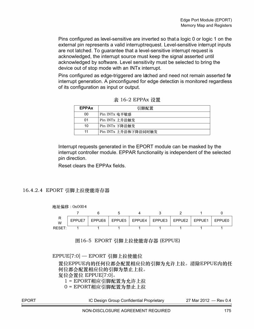
Edge Port Module (EPORT) Memory Map and Registers
Pins configured as level-sensitive are inverted so that a logic 0 or logic 1 on the external pin represents a valid interrupt request. Level-sensitive interrupt inputs are not latched. To guarantee that a level-sensitive interrupt request is acknowledged, the interrupt source must keep the signal asserted until acknowledged by software. Level sensitivity must be selected to bring the device out of stop mode with an INTx interrupt.Pins configured as edge-triggered are latched and need not remain asserted for interrupt generation. A pin configured for edge detection is monitored regardless of its configuration as input or output.
Interrupt requests generated in the EPORT module can be masked by the interrupt controller module. EPPAR functionality is independent of the selected pin direction.Reset clears the EPPAx fields.
16.4.2.4 EPORT 引脚上拉使能寄存器
图16-5 EPORT 引脚上拉使能寄存器 (EPPUE)
EPPUE[7:0] — EPORT 引脚上拉使能位置位EPPUE内的任何位都会配置相应位的引脚为允许上拉。清除EPPUE内的任何位都会配置相应位的引脚为禁止上拉。 复位会置位 EPPUE[7:0]。
1 = EPORT相应引脚配置为允许上拉0 = EPORT相应引脚配置为禁止上拉
表 16-2 EPPAx 设置EPPAx 引脚配置
00 Pin INTx 电平敏感01 Pin INTx 上升沿触发10 Pin INTx 下降沿触发11 Pin INTx 上升沿和下降沿同时触发
地址偏移 : 0x00047 6 5 4 3 2 1 0
REPPUE7 EPPUE6 EPPUE5 EPPUE4 EPPUE3 EPPUE2 EPPUE1 EPPUE0
WRESET: 1 1 1 1 1 1 1 1
EPORT IC Design Group Confidential Proprietary 27 Mar 2012 — Rev 0.4
NON-DISCLOSURE AGREEMENT REQUIRED 175
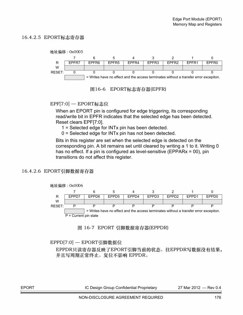
Edge Port Module (EPORT) Memory Map and Registers
16.4.2.5 EPORT标志寄存器
图16-6 EPORT标志寄存器(EPFR)
EPF[7:0] — EPORT标志位When an EPORT pin is configured for edge triggering, its corresponding read/write bit in EPFR indicates that the selected edge has been detected. Reset clears EPF[7:0].
1 = Selected edge for INTx pin has been detected.0 = Selected edge for INTx pin has not been detected.
Bits in this register are set when the selected edge is detected on the corresponding pin. A bit remains set until cleared by writing a 1 to it. Writing 0 has no effect. If a pin is configured as level-sensitive (EPPARx = 00), pin transitions do not affect this register.
16.4.2.6 EPORT引脚数据寄存器
图 16-7 EPORT 引脚数据寄存器(EPPDR)
EPPD[7:0] — EPORT引脚数据位EPPDR只读寄存器反映了EPORT引脚当前的状态。往EPPDR写数据没有结果,并且写周期正常终止。复位不影响 EPPDR。
地址偏移 : 0x00057 6 5 4 3 2 1 0
R EPFR7 EPFR6 EPFR5 EPFR4 EPFR3 EPFR2 EPFR1 EPFR0W
RESET: 0 0 0 0 0 0 0 0= Writes have no effect and the access terminates without a transfer error excepiton.
地址偏移 : 0x00067 6 5 4 3 2 1 0
R EPPD7 EPPD6 EPPD5 EPPD4 EPPD3 EPPD2 EPPD1 EPPD0W
RESET: P P P P P P P P= Writes have no effect and the access terminates without a transfer error excepiton.
P = Current pin state
EPORT IC Design Group Confidential Proprietary 27 Mar 2012 — Rev 0.4
NON-DISCLOSURE AGREEMENT REQUIRED 176

Edge Port Module (EPORT) Memory Map and Registers
16.4.2.7 EPORT数据寄存器
图 16-8 EPORT 数据寄存器 (EPDR)
EPD[7:0] — EPORT数据位写入EPDR的数据会存储在内部寄存器内;如果EPORT的任何引脚配置为输出,写入EPDR中的数据就会存储在内部寄存器中;如果任何引脚的端口被配置为输出,存储在引脚上的数据会被驱动到引脚上。读EDPR返回存储在寄存器中的数据。复位置位EPD[7:0]。
16.4.2.8 EPORT 位设置寄存器
图16-9 EPORT 位设置寄存器 (EPBSR)
EPBSR[7:0] — EPORT 位设置寄存器
1 = EPDR相应的位会被置位0 = EPDR相应的位没影响
地址偏移 : 0x00077 6 5 4 3 2 1 0
REPD7 EPD6 EPD5 EPD4 EPD3 EPD2 EPD1 EPD0
WRESET: 1 1 1 1 1 1 1 1
地址偏移 : 0x00087 6 5 4 3 2 1 0
R 0 0 0 0 0 0 0 0W EPBSR7 EPBSR6 EPBSR5 EPBSR4 EPBSR3 EPBSR2 EPBSR1 EPBSR0
RESET: 0 0 0 0 0 0 0 0
EPORT IC Design Group Confidential Proprietary 27 Mar 2012 — Rev 0.4
NON-DISCLOSURE AGREEMENT REQUIRED 177

Edge Port Module (EPORT) Memory Map and Registers
16.4.2.9 EPORT 数字滤波器控制寄存器
图 16-10 EPORT 数字滤波器控制寄存器(EPFC)
Filter_En — EPORT 数字滤波使能位
1 = EPORT 数字滤波使能0 = EPORT 数字滤波禁止
Filter_Width[6:0] — 数字滤波器的脉冲宽度选择位Filter_Width[6:0] 决定了被滤波的输入脉冲宽度。如果输入的脉冲宽度小于(Filter_Width[6:0]+2), 那么脉冲将被过滤掉。
16.4.2.10 EPORT 开漏使能寄存器
图 16-11 EPORT 开漏使能寄存器 (EPODE)
EPODE[7:0] — EPORT开漏使能位如果EPORT被配置为输出,置位EPODE的任何位都会配置相应引脚为开漏输出。清除EPODE的任何位都会配置相应引脚为CMOS输出。复位清除EPODE[7:0]。
1 = 相应的EPORT引脚配置为开漏输出0 = 相应的EPORT引脚配置为CMOS输出
地址偏移 : 0x00097 6 5 4 3 2 1 0
RFilter_Width[6:0] Filter_En
WRESET: 0 0 0 0 0 0 0 0
地址偏移 : 0x000a7 6 5 4 3 2 1 0
REPODE7 EPODE6 EPODE5 EPODE4 EPODE3 EPODE2 EPODE1 EPODE0
WRESET: 0 0 0 0 0 0 0 0
EPORT IC Design Group Confidential Proprietary 27 Mar 2012 — Rev 0.4
NON-DISCLOSURE AGREEMENT REQUIRED 178

Edge Port Module (EPORT) Memory Map and Registers
16.4.2.11 EPORT 电平极性寄存器
图16-12 EPORT电平极性寄存器 (EPLPR)
EPLPR[7:0] — EPORT电平极性位如果EPORT配置为电平触发, 置位 EPLPR的任何位都会配置相应引脚为高电平触发。清除 EPLPR的任何位都会配置相应引脚为低电平触发。 复位清除 EPLPR[7:0].
1 = 相应的EPORT引脚为高电平触发 0 = 相应的EPORT引脚为低电平触发
16.4.2.12 EPORT 位清零寄存器
图 16-13 EPORT 位清零寄存器 (EPBCR)
EPBCR[7:0] — EPORT 位清零寄存器
1 = EPDR相应位被清零0 = EPDR相应位无影响
地址偏移 : 0x000b7 6 5 4 3 2 1 0
REPLPR7 EPLPR6 EPLPR5 EPLPR4 EPLPR3 EPLPR2 EPLPR1 EPLPR0
WRESET: 0 0 0 0 0 0 0 0
地址偏移 : 0x000f7 6 5 4 3 2 1 0
R 0 0 0 0 0 0 0 0W EPBCR7 EPBCR6 EPBCR5 EPBCR4 EPBCR3 EPBCR2 EPBCR1 EPBCR0
RESET: 0 0 0 0 0 0 0 0
EPORT IC Design Group Confidential Proprietary 27 Mar 2012 — Rev 0.4
NON-DISCLOSURE AGREEMENT REQUIRED 179
Advance Information — SPI
第十七节: 串行外设接口模块 (SPI)
17.1 介绍
The serial peripheral interface (SPI) module allows full-duplex, synchronous, serial communication between the microcontroller unit(MCU) and peripheral devices. Software can poll the SPI status flags or SPI operation can be interrupt driven.
17.2 特性
主要特性包括:
• 支持主模式和从模式
• 支持线与模式
• 从模式选择输出
• Mode fault error flag with central processor unit (CPU) interrupt capability
• 在休眠模式下的SPI操作控制
• 为低功耗操作降低驱动控制
• 为飞思卡尔SPI或TI公司同步串行接口提供可编程接口操作
• Separate transmit and receive FIFOs, each 8 bits wide and 8 locations deep
• 4到16位可编程的数据帧大小
• 诊断/调试测试的内部回路测试模式
• 标准的基于FIFO的中断和传输结束中断
• 高效的DMA传输接口
• Visibility into TX and RX FIFOs for ease of debugging
• 传输定时调节的高速模式
SPI IC Design Group Confidential Proprietary Rev 0.4 — 27 Mar 2012
NON-DISCLOSURE AGREEMENT REQUIRED 180

Serial Peripheral Interface Module (SPI) Modes of Operation
17.3 操作模式
SPI模块包含以下三种模式:
1. 运行模式 — 运行模式是正常操作模式。
2. 休眠模式 — 休眠模式是一个可配置的低功耗模式。
3. 停止模式 — 停止模式下SPI是无效的。
SPI IC Design Group Confidential Proprietary 27 Mar 2012 — Rev 0.4
NON-DISCLOSURE AGREEMENT REQUIRED 181

Serial Peripheral Interface Module (SPI) Block Diagram
17.4 框图
图 17-1 SPI 框图
SPI IC Design Group Confidential Proprietary 27 Mar 2012 — Rev 0.4
NON-DISCLOSURE AGREEMENT REQUIRED 182

Serial Peripheral Interface Module (SPI) Signal Description
17.5 信号描述
信号的描述如表17-1所示。
17.5.1 MISO (主模式输入/从模式输出)
MISO 是两个SPI数据引脚中的一个。
• 主模式下,MISO 是数据输入口。
• In slave mode, MISO is the data output and is three-stated until a master drives the SS input pin low.
• In bidirectional mode, a slave MISO pin is the SISO pin (slave in/slave out).
• In a multiple-master system, all MISO pins are tied together.
17.5.2 MOSI (主模式输出/从模式输入)
MOSI 是两个SPI数据引脚中的一个。
• 在主模式下,MOSI是数据输出口。
• 在从模式下,MOSI是数据输入口。
• In bidirectional mode, a master MOSI pin is the MOMI pin (master out/master in).
• In a multiple-master system, all MOSI pins are tied together.
表 17-1 信号属性
名称 端口 功能1
说明:
1. 当SPI功能被禁止时(SPE=0),特定的SPI端口 (MISO,MOSI,SCK,SS) 为通用的GPIO口。
复位状态MISO SPIPORT[0] 主模式输入/从模式输出 0MOSI SPIPORT[1] 主模式输出/从模式输入 0SCK SPIPORT[2] 串行时钟 0SS SPIPORT[3] 从模式选择 0
SPI IC Design Group Confidential Proprietary 27 Mar 2012 — Rev 0.4
NON-DISCLOSURE AGREEMENT REQUIRED 183

Serial Peripheral Interface Module (SPI) Signal Description
17.5.3 SCK (S串行时钟)
SCK引脚是一个为了同步主从设备之间传输的时钟引脚。
• 主模式下,SCK 为输出。
• 从模式下,SCK 为输入。
• In a multiple-master system, all SCK pins are tied together.
17.5.4 SS (从模式选择)
在主模式下, SS引脚可以是:
• A mode-fault input
• 通用输入
• 通用输出
• 从选择输出
在从模式下, SS 引脚始终是从选择输入。
SPI IC Design Group Confidential Proprietary 27 Mar 2012 — Rev 0.4
NON-DISCLOSURE AGREEMENT REQUIRED 184
X84L
线条
X84L
线条

Serial Peripheral Interface Module (SPI) Memory Map and Registers
0x001e
SPI 波特率寄存器
SPI 控制寄存器 2(SPICR2)
(SPIBR)
0x001c
0x0017
0x0016
0x0010~11
0x000d~f
0x000c
0x0004
0x0003
0x0002
0x0001
17.6 内存映射与寄存器
表 17-2
表 17-2 SPI 内存映射
地址偏移 访问权
SPI 控制寄存器1(SPICR1)
S/U
0x0000
S/U
SPI 帧寄存器 (SPIFR)
0x0007
SPI RXFIFO 控制寄存器(SPIRXFCR) S/U
0x0006
SPI TXFIFO C控制寄存器(SPITXFCR) S/U0x0005
SPI RX FIFO 超时计数器寄存器(SPIRXFTOCTR) S/U
SPI TX FIFO 超时计数器寄存器(SPITXFTOCTR) S/U
0x000b
SPI 端口数据方向寄存器 (SPIDDR) S/U
0x000a
(SPIPURD) S/U0x0009
SPI After SCK Delay Register (SPIASCDR) S/U
0x0008
SPI Before SCK Delay Register (SPIBSCDR) S/U
SPI 发送计数器寄存器 (SPITCNT)
S/USPI 端口数据寄存器 (SPIPORT)
S/U
SPI 数据寄存器 (SPIDR) S/U
0x0014
SPI TX FIFO 状态寄存器(SPITXFSR)
S/U
SPI RX FIFO 状态寄存器 (SPIRXFSR) S/U
SPI 状态寄存器(SPISR)
S/U
0x0018
SPI 中断开心寄存器 (SPIICR)
S/U
0x0019
SPI FIFO D调试控制寄存器(SPIFDCR)
S/U
0x001a
SPI DMA阈值寄存器 (SPIDMATHR)
S/U
0x001b
SPI DMA 控制寄存器(SPIDMACR)
S/U
SPI TX FIFO 调试寄存器 (SPITXFDBGR)
S/USPI RX FIFO 调试寄存器 (SPIRXFDBGR)
S/U
SPI 上拉和降低驱动寄存器
S/U
S/U
SPI IC Design Group Confidential Proprietary 27 Mar 2012 — Rev 0.4
NON-DISCLOSURE AGREEMENT REQUIRED 185

Serial Peripheral Interface Module (SPI) Memory Map and Registers
17.6.1 SPI 控制寄存器1
图 17-2 SPI 控制寄存器1 (SPICR1)
读:任何时候
写:任何时候
SPIE — SPI 中断使能位SPIE 位使能EOTF 标志以产生中断请求。复位清除SPIE位。
1 = EOTF中断请求使能0 = EOTF中断请求禁止
SPE — SPI系统使能位The SPE bit enables the SPI and dedicates SPI port pins [3:0] to SPI functions. When SPE is clear, the SPI system is initialized but in a low-power disabled state. Reset clears SPE.
1 = 启用SPI 0 = 禁止SPI
SWOM — SPI线与模式位SWOM位配置SPI端口引脚[3:0]的输出缓冲器为开漏输出。SWOM控制 SPI端口引脚[3:0]是SPI输出还是通用输出。 复位清除SWOM。
1 = SPI端口引脚[3:0]的输出缓冲器为开漏。0 = SPI端口引脚[3:0]的输出缓冲器为CMOS驱动。
NOTE: The SWOM bit has no effect in this part.
MSTR — 主模式选择位MSTR位决定了SPI是主模式操作还是从模式操作。 复位清除 MSTR.
1 = 配置为主模式0 = 配置为从模式
地址偏移: 0x0000Bit 7 6 5 4 3 2 1 Bit 0
Read:SPIE SPE SWOM MSTR CPOL CPHA SSOE LSBFE
Write:RESET: 0 0 0 0 0 1 0 0
SPI IC Design Group Confidential Proprietary 27 Mar 2012 — Rev 0.4
NON-DISCLOSURE AGREEMENT REQUIRED 186
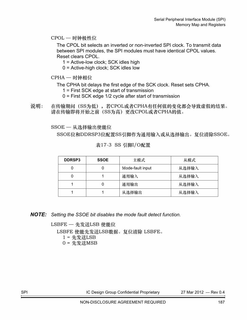
Serial Peripheral Interface Module (SPI) Memory Map and Registers
CPOL — 时钟极性位The CPOL bit selects an inverted or non-inverted SPI clock. To transmit data between SPI modules, the SPI modules must have identical CPOL values. Reset clears CPOL.
1 = Active-low clock; SCK idles high0 = Active-high clock; SCK idles low
CPHA — 时钟相位The CPHA bit delays the first edge of the SCK clock. Reset sets CPHA.
1 = First SCK edge at start of transmission0 = First SCK edge 1/2 cycle after start of transmission
说明: 在传输期间(SS为低),若CPOL或者CPHA有任何值的变化都会导致虚假的结果。请在传输即将开始之前(SS为高)更改CPOL或者CPHA的值。
SSOE — 从选择输出使能位SSOE位和DDRSP3位配置SS引脚作为通用输入或从选择输出。复位清除SSOE。
NOTE: Setting the SSOE bit disables the mode fault detect function.
LSBFE — 先发送LSB 使能位LSBFE 使能先发送LSB数据。复位清除 LSBFE。
1 = 先发送LSB0 = 先发送MSB
表17-3 SS 引脚I/O配置
DDRSP3 SSOE 主模式 从模式
0 0 Mode-fault input 从选择输入
0 1 通用输入 从选择输入
1 0 通用输出 从选择输入
1 1 从选择输出 从选择输入
SPI IC Design Group Confidential Proprietary 27 Mar 2012 — Rev 0.4
NON-DISCLOSURE AGREEMENT REQUIRED 187
X84L
线条
X84L
线条
X84L
线条

Serial Peripheral Interface Module (SPI) Memory Map and Registers
17.6.2 SPI 控制寄存器 2
图 17-3 SPI 控制寄存器 2 (SPICR2)
读: 任何时候
写: 任何时候
GT — Guard Time Bits
GT = (GT[5:3]+1)*2(GT[2:0]+1)
SPISDOZ — 休眠模式下SPI停止当CPU处于休眠模式下,SPIDOZ 位停止SPI时钟。
1 = 休眠模式下SPI无效0 = 休眠模式下SPI有效
SPC0 — 串行引脚控制位0The SPC0 bit enables the bidirectional pin configurations shown in Table 17-4.
地址偏移: 0x0001Bit7 6 5 4 3 2 1 Bit0
Read:GT[5:0] SPISDOZ SPC0
Write:RESET: 0 0 0 0 0 0 0 0
= Writes have no effect and the access terminates without a transfer error exception.
Table 17-4 Bidirectional Pin Configurations
Pin Mode SPC0 MSTR MISO Pin1 MOSI Pin2 SCK Pin3 SS Pin4
ANormal 0
0 Slave data output
Slave data input SCK input Slave-select input
B 1 Master data input
Master data output
SCK output
MODF/GP input (DDRSP3 = 0) or GP output (DDRSP3 = 1)
CBidirectional 1
0 Slave data I/O GP5 I/O SCK input Slave-select input
D 1 GP I/O Master data I/O
SCK output
MODF/GP input (DDRSP3 = 0) or GP output (DDRSP3 = 1)
NOTES:1. Slave output is enabled if SPIDDR bit 0 = 1, SS = 0, and MSTR = 0 (A, C).2. Master output is enabled if SPIDDR bit 1 = 1 and MSTR = 1 (B, D).3. SCK output is enabled if SPIDDR bit 2 = 1 and MSTR = 1 (B, D).4. SS output is enabled if SPIDDR bit 3 = 1, SPICR1 bit 1 (SSOE) = 1, and MSTR = 1 (B, D). MODF input is enabled if SPI DDR bit 3 = 0 and SSOE = 0. GP input is enabled if SPI DDR bit 3 = 0 and SSOE = 1.5. GP = General-purpose
SPI IC Design Group Confidential Proprietary 27 Mar 2012 — Rev 0.4
NON-DISCLOSURE AGREEMENT REQUIRED 188

Serial Peripheral Interface Module (SPI) Memory Map and Registers
17.6.3 SPI 波特率寄存器
图 17-4 SPI 波特率寄存器 (SPIBR)
读:任何时候
写:任何时候;往未定义的位写数据是无效的。
SPPR[6:4] — SPI 波特率预选位SPPR[6:4]和SPR[2:0]位共同选择SPI时钟因子,如表17-5所示。复位可清除SPPR[6:4]和 SPR[2:0],并且SPI的时钟因子为2。
SPR[2:0] — SPI 波特率位SPPR[6:4]和SPR[2:0]位共同选择SPI时钟因子,如表17-5所示。复位可清除SPPR[6:4]和 SPR[2:0],并且SPI的时钟因子为2。
注意: 在传输过程中,往SPIBR写入数据可能会导致错误的结果。
地址偏移: 0x0002Bit 7 6 5 4 3 2 1 Bit 0
Read: 0SPPR6 SPPR5 SPPR4
0SPR2 SPR1 SPR0
Write:RESET: 0 0 0 0 0 0 0 0
= Writes have no effect and the access terminates without a transfer error exception.
表17-5 SPI波特率选择 (10-MH z 模块时钟)
SPPR[6:4] SPR[2:0] SPI时钟因子 波特率 SPPR[6:4] SPR[2:0] SPI 时钟因子 波特率
000 000 2 5 MHz 100 000 10 1 MHz
000 001 4 2.5 MHz 100 001 20 0.5 MHz
000 010 8 1.25 MHz 100 010 40 0.25 MHz
000 011 16 0.625 MHz 100 011 80 125 kHz
000 100 32 0.31 MHz 100 100 160 62.5 kHz
000 101 64 156.25 kHz 100 101 320 31.25 kHz
000 110 128 78.125 kHz 100 110 640 15.625 kHz
000 111 256 39.06 kHz 100 111 1280 7.81 kHz
001 000 4 2.5 MHz 101 000 12 833.33 kHz
SPI IC Design Group Confidential Proprietary 27 Mar 2012 — Rev 0.4
NON-DISCLOSURE AGREEMENT REQUIRED 189

Serial Peripheral Interface Module (SPI) Memory Map and Registers
001 001 8 1.25 MHz 101 001 24 416.67 kHz
001 010 16 0.625 MHz 101 010 48 208.33 kHz
001 011 32 0.31 MHz 101 011 96 104.17 kHz
001 100 64 156.25 kHz 101 100 192 52.08 kHz
001 101 128 78.125 kHz 101 101 384 26.04 kHz
001 110 256 39.06 kHz 101 110 768 13.02 kHz
001 111 512 19.53 kHz 101 111 1536 6.51 kHz
010 000 6 1.67 MHz 110 000 14 714.29 kHz
010 001 12 0.83 MHz 110 001 28 357.14 kHz
010 010 24 0.42 MHz 110 010 56 178.57 kHz
010 011 48 208.33 kHz 110 011 112 89.29 kHz
010 100 96 104.17 kHz 110 100 224 44.64 kHz
010 101 192 52.08 kHz 110 101 448 22.32 kHz
010 110 384 26.04 kHz 110 110 896 11.16 kHz
010 111 768 13.02 kHz 110 111 1792 5.58 kHz
011 000 8 1.25 MHz 111 000 16 0.625 MHz
011 001 16 0.625 MHz 111 001 32 0.31 MHz
011 010 32 0.31 MHz 111 010 64 156.25 kHz
011 011 64 156.25 kHz 111 011 128 78.125 kHz
011 100 128 78.125 kHz 111 100 256 39.06 kHz
011 101 256 39.06 kHz 111 101 512 19.53 kHz
011 110 512 19.53 kHz 111 110 1024 9.77 kHz
011 111 1024 9.77 kHz 111 111 2048 4.88 kHz
表17-5 SPI波特率选择 (10-MH z 模块时钟)
SPPR[6:4] SPR[2:0] SPI 时钟因子 波特率 SPPR[6:4] SPR[2:0] SPI 时钟
因子 波特率
SPI IC Design Group Confidential Proprietary 27 Mar 2012 — Rev 0.4
NON-DISCLOSURE AGREEMENT REQUIRED 190

Serial Peripheral Interface Module (SPI) Memory Map and Registers
17.6.4 SPI 帧寄存器
图17-5 SPI 帧寄存器 (SPIFR)
读:任何时候
写:任何时候
CONT—Continuous peripheral chip select enable
1 = Keep peripheral chip select signal low between transfers until EOTF is set
0 = Return peripheral chip select signal to high between transfers
GTE—Guard Time Enable
1 = Guard Time is Enabled
0 = Guard Time is Disabled
LBM—Loop Back Mode
1 = Loop Back Mode
0 = Normal Mode
FFSEL— Frame Format Select
1 = TI frame format is selected
0 = FREESCALE frame format is selected
FMSZ[3:0] — Frame SizeThe FMSZ[3:0] bits control the frame data length from 4 to 16bits. 0x3 sets the frame length to 4bits and 0xf sets it to 16 bits. meanwhile case 0x0~0x2 will set the frame to 4 bit long automatically.
NOTE:
地址偏移: 0x0003Bit 7 6 5 4 3 2 1 Bit 0
Read:CONT GTE LBM FFSEL FMSZ3 FMSZ2 FMSZ1 FMSZ0
Write:RESET: 0 1 0 0 0 1 1 1
Pin function:
SPI IC Design Group Confidential Proprietary 27 Mar 2012 — Rev 0.4
NON-DISCLOSURE AGREEMENT REQUIRED 191

Serial Peripheral Interface Module (SPI) Memory Map and Registers
17.6.5 SPI RX FIFO 控制寄存器
Figure 17-6 SPI RX FIFO 控制寄存器 (SPIRXFCR)
读: 任何时候
写: 任何时候
RXFCLR — RX FIFO 清除往该位写1会复位RX FIFO。
RXFOVIE — RX FIFO 溢出中断使能1 = 允许RX FIFO 溢出中断0 = 禁止RX FIFO 溢出中断
RXFUDIE — RX FIFO 下溢中断使能1 = 允许RX FIFO 下溢中断0 = 允许RX FIFO 下溢中断
RXFSTHIE — RX FIFO 服务阈值中断使能1 = 允许RX FIFO 服务阈值中断0 = 禁止RX FIFO 服务阈值中断
RXFSTH[2:0] — RX FIFO 服务阈值
Once effective data number in RX FIFO is above or equal the threshold specified, RX FIFO Service Flag asserted.
data number=RXFSTH[2:0]+1
NOTE:
地址偏移: 0x0004Bit 7 6 5 4 3 2 1 Bit 0
Read:RXFCLR RXFOVIE RXFUDIE RXFSTHIE
0RXFSTH2 RXFSTH1 RXFSTH0
Write:RESET: 0 0 0 0 0 0 0 0
= Writes have no effect and the access terminates without a transfer error exception.
SPI IC Design Group Confidential Proprietary 27 Mar 2012 — Rev 0.4
NON-DISCLOSURE AGREEMENT REQUIRED 192

Serial Peripheral Interface Module (SPI) Memory Map and Registers
17.6.6 SPI TX FIFO 控制寄存器
图 17-7 SPI TX FIFO 控制寄存器 (SPITXFCR)
读: 任何时候
写: 任何时候
TXFCLR — TX FIFO 清零往该位写1会复位TXFIFO。
TXFOVIE — TX FIFO 溢出中断使能1 = 允许TX FIFO 溢出中断0 = 禁止TX FIFO 溢出中断
TXFUDIE — TX FIFO 下溢中断使能1 = 允许TX FIFO 下溢中断0 = 禁止TX FIFO 下溢中断
TXFSTHIE — TX FIFO 服务阈值中断使能1 = 允许TX FIFO 服务阈值中断0 = 禁止TX FIFO 服务阈值中断
TXFSTH[2:0] — TX FIFO Service Threshold
Once effective data number in TX FIFO is below or equal the threshold specified, TX FIFO Service Flag asserted.
data number=TXFSTH[2:0]
NOTE:
地址偏移: 0x0005Bit 7 6 5 4 3 2 1 Bit 0
Read:TXFCLR TXFOVIE TXFUDIE TXFSTHIE
0TXFSTH2 TXFSTH1 TXFSTH0
Write:RESET: 0 0 0 0 0 0 0 0
= Writes have no effect and the access terminates without a transfer error exception.
SPI IC Design Group Confidential Proprietary 27 Mar 2012 — Rev 0.4
NON-DISCLOSURE AGREEMENT REQUIRED 193

Serial Peripheral Interface Module (SPI) Memory Map and Registers
17.6.7 SPI RX FIFO 超时计数器寄存器
图 17-8 SPI RX FIFO 超时计数器寄存器(SPIRXFTOCTR)
读: 任何时候
写: 任何时候
SPIRXFTOCTR[5:0]设置SPI RX FIFO超时计数器的数值。一旦RX FIFO不为空,计数器就会工作。如果直到计数器计数下降到0,而RX FIFO又没有任何操作时, SPISR寄存器的 RXF_TIMEOUT标志位会被置位。
RXFTOIE — RX FIFO 超时中断使能1 = 允许RX FIFO 超时中断0 = 禁止RX FIFO 超时中断
RXFTOE — RX FIFO 超时功能使能1 = RX FIFO超时功能使能0 = RX FIFO超时功能禁止
地址偏移: 0x0006Bit 7 6 5 4 3 2 1 Bit 0
Read:RXFTOIE RXFTOE 5 4 3 2 1 0
Write:RESET: 0 0 1 0 0 0 0 0
SPI IC Design Group Confidential Proprietary 27 Mar 2012 — Rev 0.4
NON-DISCLOSURE AGREEMENT REQUIRED 194

Serial Peripheral Interface Module (SPI) Memory Map and Registers
17.6.8 SPI TX FIFO 超时计数器寄存器
图 17-9 SPI TX FIFO 超时计数器寄存器 (SPITXFTOCTR)
读: 任何时候
写: 任何时候
SPITXFTOCTR[5:0]设置SPI TX FIFO超时计数器的数值。一旦TX FIFO不为空,计数器就会工作。如果直到计数器计数下降到0,而TX FIFO又没有任何操作时, SPISR寄存器的 TXF_TIMEOUT标志位会被置位。
TXFTOIE — TX FIFO 超时中断使能1 = TX FIFO 超时中断使能0 = TX FIFO 超时中断禁止
TXFTOE — TX FIFO 超时功能使能1 = TX FIFO 超时功能使能0 = TX FIFO 超时功能禁止
地址偏移: 0x0007Bit 7 6 5 4 3 2 1 Bit 0
Read:TXFTOIE TXFTOE 5 4 3 2 1 0
Write:RESET: 0 0 1 0 0 0 0 0
SPI IC Design Group Confidential Proprietary 27 Mar 2012 — Rev 0.4
NON-DISCLOSURE AGREEMENT REQUIRED 195

Serial Peripheral Interface Module (SPI) Memory Map and Registers
17.6.9 SPI 端口数据方向寄存器
图 17-10 SPI 端口数据方向寄存器 (SPIDDR)
读: 任何时候
写: 任何时候
RSVD[7:4] — 保留
写这些可读写位可以更新它们的值,但对功能无影响。
DDRSP[3:0] — 数据方向位DDRSP[3:0]位控制着SPI引脚的数据方向。 复位清除 DDRSP[3:0]。
1 = 相应引脚配置为输出0 = 相应引脚配置为输入
在从模式下,DDRSP3没有任何意义和影响。在主模式下,DDRSP3和SSOE位决定了SPI端口的第3引脚是模式错误输入,通用输入,通用输出还是从模式选择输出。
NOTE: When the SPI is enabled (SPE = 1), the MISO, MOSI, and SCK pins:
• Are inputs if their SPI functions are input functions regardless of the state of their DDRSP bits.
• Are outputs if their SPI functions are output functions only if their DDRSP bits are set
地址偏移: 0x0008Bit 7 6 5 4 3 2 1 Bit 0
Read:RSVD7 RSVD6 RSVD5 RSVD4 DDRSP3 DDRSP2 DDRSP1 DDRSP0
Write:RESET: 0 0 0 0 0 0 0 0
Pin function: SS SCKMOSI/ MISO/MOMI SISO
SPI IC Design Group Confidential Proprietary 27 Mar 2012 — Rev 0.4
NON-DISCLOSURE AGREEMENT REQUIRED 196

Serial Peripheral Interface Module (SPI) Memory Map and Registers
17.6.10 SPI 上拉与降低驱动寄存器
图17-11 SPI 上拉与降低驱动寄存器 (SPIPURD)
读:任何时候;
写:任何时候;往未定义的位写入数据是无意义的。
HS— 高速模式使能位
主模式下置位HS 使得MSPD[1:0]生效。
1 = 允许高速模式 0 = 禁止高速模式
PSW— 引脚开关位
MOSI切换到MISO,MISO切换到MOSI。
1 = 允许开关 0 = 禁止开关
MSPD[1:0] — SPI Master Sample Point Delay Specify the number of system clock cycles delayed for SCK sample edge 0x0=no delay;0x1=1 cycle delay;0x2=2 cycle delay;0x3=2 cycle delay;
PDPSP — SPI 端口下拉使能位1 = Pulldown devices enabled for SPIPORT bits [3:0]0 = Pulldown devices disabled for SPIPORT bits [3:0]
PUPSP — SPI 端口上拉使能位1 = Pullup devices enabled for SPIPORT bits [3:0]0 = Pullup devices disabled for SPIPORT bits [3:0]
地址偏移: 0x0009Bit 7 6 5 4 3 2 1 Bit 0
Read:HS PSW RESERVED MSPD1 MSPD0 PDPSP PUPSP
Write:RESET: 0 0 0 0 0 0 0 1
SPI IC Design Group Confidential Proprietary 27 Mar 2012 — Rev 0.4
NON-DISCLOSURE AGREEMENT REQUIRED 197

Serial Peripheral Interface Module (SPI) Memory Map and Registers
17.6.11 SPI After SCK Delay Register
Figure 17-12 SPI After SCK Delay Register (SPIASCDR)
Read: Anytime
Write: Anytime
ASCDE—After SCK Delay Enable
1 = After SCK Delay is Enabled
0 = After SCK Delay is Disabled
PASCD[6:4] — SPI After SCK Delay Preselection BitsThe PASCD[6:4] and ASCD[2:0] bits select the SPI after SCK delay divisor.
ASCD[2:0] — SPI After SCK Delay Bits ASCD = (PASCD[6:4]+1)*2(ASCD[2:0]+1);and tT =0.5*SCK+ ASCD
NOTE:
Address Offset: 0x000aBit 7 6 5 4 3 2 1 Bit 0
Read:ASCDE PASCD6 PASCD5 PASCD4
0ASCD2 ASCD1 ASCD0
Write:RESET: 0 0 0 0 0 0 0 0
= Writes have no effect and the access terminates without a transfer error exception.
SPI IC Design Group Confidential Proprietary 27 Mar 2012 — Rev 0.4
NON-DISCLOSURE AGREEMENT REQUIRED 198

Serial Peripheral Interface Module (SPI) Memory Map and Registers
17.6.12 SPI Before SCK Delay Register
Figure 17-13 SPI Before SCK Delay Register (SPIBSCDR)
Read: Anytime
Write: Anytime
BSCDE—Before SCK Delay Enable
1 = Before SCK Delay is Enabled
0 = Before SCK Delay is Disabled
PBSCD[6:4] — SPI Before SCK Delay Preselection BitsThe PBSCD[6:4] and BSCD[2:0] bits select the SPI before SCK delay divisor.
BSCD[2:0] — SPI Before SCK Delay Bits BSCD = (PBSCD[6:4]+1)*2(BSCD[2:0]+1) ;and tL= 0.5*SCK+BSCD
NOTE:
Address Offset: 0x000bBit 7 6 5 4 3 2 1 Bit 0
Read:BSCDE PBSCD6 PBSCD5 PBSCD4
0BSCD2 BSCD1 BSCD0
Write:RESET: 0 0 0 0 0 0 0 0
= Writes have no effect and the access terminates without a transfer error exception.
SPI IC Design Group Confidential Proprietary 27 Mar 2012 — Rev 0.4
NON-DISCLOSURE AGREEMENT REQUIRED 199

Serial Peripheral Interface Module (SPI) Memory Map and Registers
17.6.13 SPI 端口数据寄存器
图 17-14 SPI 端口数据寄存器(SPIPORT)
读: 任何时候
写: 任何时候
RSVD[7:4]— 保留
写这些可读写位可以更新它们的值,但对功能无影响。
PORTSP[3:0] — SPI 端口数据位
Data written to SPIPORT drives pins only when they are configured as general-purpose outputs.
Reading an input (DDRSP bit clear) returns the pin level; reading an output (DDRSP bit set) returns the pin driver input level.
当引脚配置为SPI输出时,往 PORTSP[3:0]写数据不会不改变其引脚状态。
SPIPORT I/O 口的功能取决于SPICR1寄存器的SPE位的状态和SPIDDR寄存器的DDRSP位的状态。
地址偏移: 0x000cBit 7 6 5 4 3 2 1 Bit 0
Read:RSVD7 RSVD6 RSVD5 RSVD4 PORTSP3 PORTSP2 PORTSP1 PORTSP0
Write:RESET: 0 0 0 0 0 0 0 0
Pin function: SS SCKMOSI/ MISO/MOMI SISO
SPI IC Design Group Confidential Proprietary 27 Mar 2012 — Rev 0.4
NON-DISCLOSURE AGREEMENT REQUIRED 200
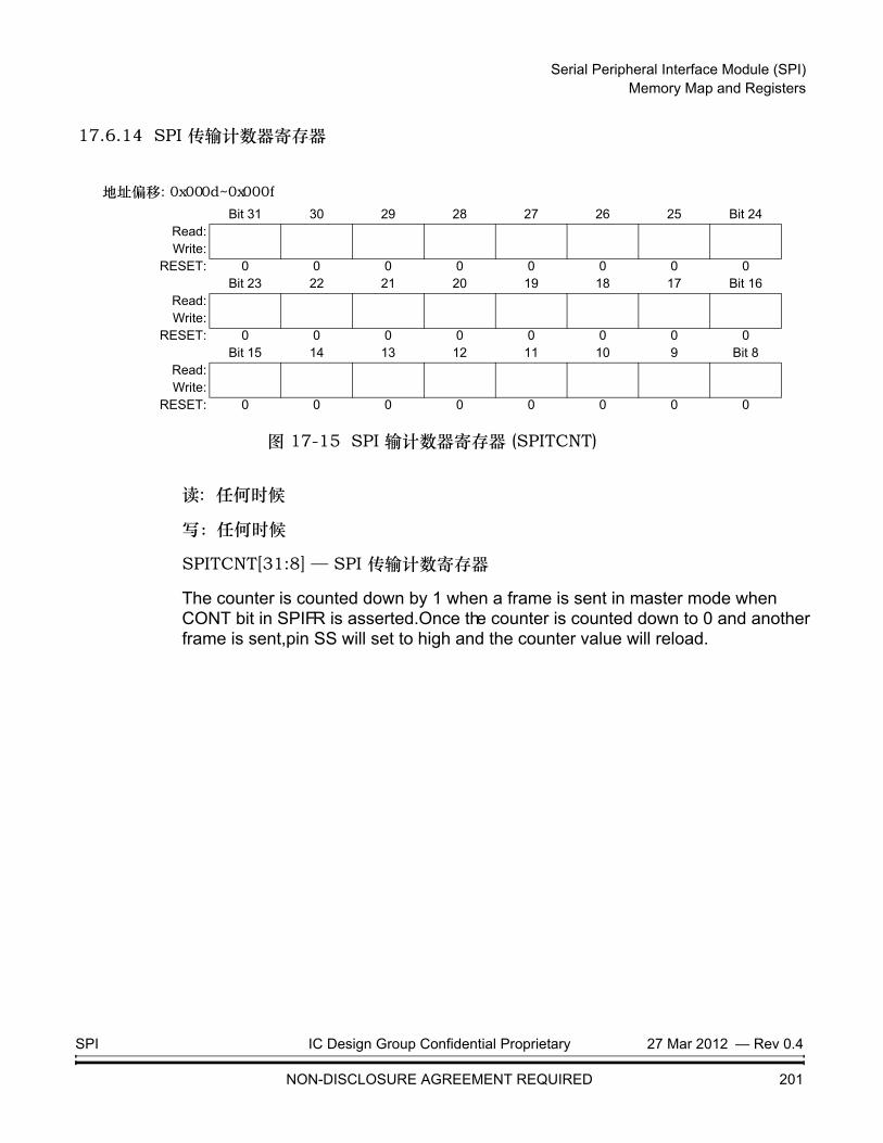
Serial Peripheral Interface Module (SPI) Memory Map and Registers
17.6.14 SPI 传输计数器寄存器
图 17-15 SPI 输计数器寄存器 (SPITCNT)
读: 任何时候
写:任何时候
SPITCNT[31:8] — SPI 传输计数寄存器
The counter is counted down by 1 when a frame is sent in master mode when CONT bit in SPIFR is asserted.Once the counter is counted down to 0 and another frame is sent,pin SS will set to high and the counter value will reload.
地址偏移: 0x000d~0x000fBit 31 30 29 28 27 26 25 Bit 24
Read:Write:
RESET: 0 0 0 0 0 0 0 0Bit 23 22 21 20 19 18 17 Bit 16
Read:Write:
RESET: 0 0 0 0 0 0 0 0Bit 15 14 13 12 11 10 9 Bit 8
Read:Write:
RESET: 0 0 0 0 0 0 0 0
SPI IC Design Group Confidential Proprietary 27 Mar 2012 — Rev 0.4
NON-DISCLOSURE AGREEMENT REQUIRED 201

Serial Peripheral Interface Module (SPI) Memory Map and Registers
17.6.15 SPI 数据寄存器
地址偏移: 0x0010
图17-16 SPI数据寄存器(SPIDR)
读: 任何时候
写: 任何时候
SPIDR is both the input and output register for SPI data. Writing to SPIDR will fill the TX FIFO while reading from SPIDR will drain the RX FIFO.
Bit 15 14 13 12 11 10 9 Bit 8Read:
15 14 13 12 11 10 9 8Write:
RESET: 0 0 0 0 0 0 0 0Bit 7 6 5 4 3 2 1 Bit 0
Read:7 6 5 4 3 2 1 0
Write:RESET: 0 0 0 0 0 0 0 0
SPI IC Design Group Confidential Proprietary 27 Mar 2012 — Rev 0.4
NON-DISCLOSURE AGREEMENT REQUIRED 202

Serial Peripheral Interface Module (SPI) Memory Map and Registers
17.6.16 SPI 状态寄存器
地址偏移: 0x0014
图 17-17 SPI 状态寄存器(SPISR)
读: 任何时候 写: w1c意味着写1将清除相应的标志
SPIF — SPI 结束标志The SPIF flag is set after each single transfer.Clear SPIF by read SPIF and then access to SPIDR.
1 = a single transfer has finished0 = a single transfer has not finished or no transfer
EOTF — 传输结束标志当TX FIFO中的所有数据传输完了,EOTF会被置位。
1 = 传输结束0 = 传输未结束或还没开始传输
往该位写1或往SPIDR写数据将清除这个标志。
FLOST — Frame Lost
When SPI is in slave mode and no valid data is in the TX FIFO,if the master start a transfer at this time,then SPI will return last received data to the master and FLOST is set. If the FLOSTIE bit is also set,FLOST generates an interrupt request.
1 = 出现帧丢失0 = 未出现帧丢失
往该位写1会清除该标志。
MODF — Mode Fault Flag
Bit 15 14 13 12 11 10 9 Bit 8Read: TXFTO TXFOVF TXFUDF TXFSER RXFTO RXFOVF RXFUDF RXFSERWrite: w1c w1c w1c w1c w1c w1c
RESET: 0 0 0 0 0 0 0 0
Bit 7 6 5 4 3 2 1 Bit 0Read: SPIF FLOST EOTF MODF TXFFULL TXFEMP RXFFULL RXFEMPWrite: w1c w1c
RESET: 0 0 0 0 0 1 0 1
= Writes have no effect and the access terminates without a transfer error exception.
SPI IC Design Group Confidential Proprietary 27 Mar 2012 — Rev 0.4
NON-DISCLOSURE AGREEMENT REQUIRED 203

Serial Peripheral Interface Module (SPI) Memory Map and Registers
The MODF flag is set when the SS pin of a master SPI is driven low and the SS pin is configured as a mode-fault input. If the SPIE bit is also set, MODF generates an interrupt request. A mode fault clears the SPE, MSTR, and DDRSP[2:0] bits. Clear MODF by reading SPISR with MODF set and then writing to SPICR1. Reset clears MODF.
1 = Mode fault0 = No mode fault
TXFFULL — TX FIFO 满标志
1 = TX FIFO 满0 = TX FIFO 未满
TXFEMP — TX FIFO 空标志
1 = TX FIFO 空0 = TX FIFO 未空
RXFFULL — RX FIFO 满标志
1 = TX FIFO 满0 = TX FIFO 未满
RXFEMP — RX FIFO 空标志
1 = RX FIFO 空0 = RX FIFO 未空
TXFTO — TX FIFO 超时
1 = TX FIFO 出现超时0 = TX FIFO 未出现超时
往该位写1或往SPIDR写数据将清除这个标志。
TXFOVF — TX FIFO 溢出标志
1 = TX FIFO 出现溢出0 = TX FIFO 未出现溢出
TXFUDF — TX FIFO 下溢标志
1 = TX FIFO 出现下溢0 = TX FIFO 未出现下溢
TXFSER — TX FIFO 服务标志
1 = TX FIFO 数据数量小于或等于TXFSTH
SPI IC Design Group Confidential Proprietary 27 Mar 2012 — Rev 0.4
NON-DISCLOSURE AGREEMENT REQUIRED 204

Serial Peripheral Interface Module (SPI) Memory Map and Registers
0 = TX FIFO 数据数量大于TXFSTH
RXFTO — RX FIFO 超时
1 = RX FIFO 出现超时0 = RX FIFO 未出现超时
write 1 to the bit or read from SPIDR will clear this flag
RXFOVF — RX FIFO 溢出标志
1 = RX FIFO 出现溢出0 = RX FIFO 未出现溢出
RXFUDF — RX FIFO 下溢标志
1 = RX FIFO 出现下溢0 = RX FIFO 未出现下溢
RXFSER — RX FIFO 服务标志
1 = RX FIFO 数据数量大于RXFSTH0 = RX FIFO 数据数量小于或等于RXFST
17.6.17 SPI RX FIFO 状态寄存器
图 17-18 SPI RX FIFO 状态寄存器 (SPIRXFSR)
读:任何时候 写:无意义,无影响
RXNXTP[2:0] — RX 下一指针表示将要被读出的数据的 RX FIFO 指针。
RXFCTR[3:0] — RX FIFO 计数器指明了RX FIFO 的数据寄存器
地址偏移: 0x0016Bit 7 6 5 4 3 2 1 Bit 0
Read: 0 RXNXTP2 RXNXTP1 RXNXTP0 RXFCTR3 RXFCTR2 RXFCTR1 RXFCTR0Write:
RESET: 0 0 0 0 0 0 0 0
= Writes have no effect and the access terminates without a transfer error exception.
SPI IC Design Group Confidential Proprietary 27 Mar 2012 — Rev 0.4
NON-DISCLOSURE AGREEMENT REQUIRED 205

Serial Peripheral Interface Module (SPI) Memory Map and Registers
17.6.18 SPI TX FIFO 状态寄存器
图 17-19 SPI TX FIFO 状态寄存器(SPITXFSR)
读:任何时候 写:无意义,无影响
TXNXTP[2:0] — TX 下一指针表示将要被读出的数据的 TX FIFO指针。
TXFCTR[3:0] — TX FIFO CounterIndicates the TX FIFO data counter.
17.6.19 SPI DMA 控制寄存器
地址偏移: 0x0018
图 17-20 SPI DMA 控制寄存器(SPIDMACR)
读: 任何时候
写: 任何时候
TXDMAE — TX FIFO DMA 请求使能1 = 允许TX DMA请求0 = 禁止TX DMA请求
RXDMAE — RX FIFO DMA 请求使能1 = 允许RX DMA请求0 = 禁止RX DMA请求
地址偏移: 0x0017Bit 7 6 5 4 3 2 1 Bit 0
Read: 0 TXNXTP2 TXNXTP1 TXNXTP0 TXFCTR3 TXFCTR2 TXFCTR1 TXFCTR0Write:
RESET: 0 0 0 0 0 0 0 0
= Writes have no effect and the access terminates without a transfer error exception.
Bit 7 6 5 4 3 2 1 Bit 0Read: 0 0 0 0 0 0
TXDMAE RXDMAEWrite:
RESET: 0 0 0 0 0 0 0 0
SPI IC Design Group Confidential Proprietary 27 Mar 2012 — Rev 0.4
NON-DISCLOSURE AGREEMENT REQUIRED 206

Serial Peripheral Interface Module (SPI) Memory Map and Registers
该位指定的RX FIFO数据数量阀值。一旦RX FIFO中的数据数量大于阀值
SPIDMACR寄存器中的RXDMAE位会被置位,SPI会向DMA发送RX DMA请求。
写:任何时候
读:任何时候
RXDMATH[2:0] — RX DMA 阈值
数据数量=TXFDMATH[2:0]
17.6.20 SPI DMA 阈值寄存器
地址偏移: 0x0019
图 17-21 SPI DMA 阈值寄存器 (SPIDMATHR)
SPIDMACR寄存器中的TXDMAE位会被置位,SPI会向DMA发送TX DMA请求。
TXDMATH[2:0] — TX DMA 阈值
该位指定的TX FIFO数据数量阈值。一旦TX FIFO中的数据数量小于阈值,
17.6.21 SPI FIFO 调试控制寄存器
地址偏移: 0x001a
图17-22 SPI FIFO 调试控制寄存器 (SPIFDCR)
读: 任何时候
写: 任何时候
Bit 7 6 5 4 3 2 1 Bit 0Read: 0 TXDMATH
2TXDMATH
1TXDMATH
00 RXDMATH
2RXDMATH
1RXDMATH
0Write:RESET: 0 0 0 0 0 0 0 0
Bit 7 6 5 4 3 2 1 Bit 0Read: 0
TXFIDX2 TXFIDX1 TXFIDX00
RXFIDX2 RXFIDX1 RXFIDX0Write:
RESET: 0 0 0 0 0 0 0 0
数据数量=RXFDMATH[2:0]+1
SPI IC Design Group Confidential Proprietary 27 Mar 2012 — Rev 0.4
NON-DISCLOSURE AGREEMENT REQUIRED 207

Serial Peripheral Interface Module (SPI) Memory Map and Registers
TXFIDX[2:0] — TX FIFO Index
Specify the data index to be read from TX FIFO to SPITXFDBGR.
RXFIDX[2:0] — RX FIFO Index
Specify the data index to be read from RX FIFO to SPIRXFDBGR.
17.6.22 SPI 中断控制寄存器
地址偏移: 0x001b
图 17-23 SPI 中断控制寄存器 (SPIICR)
读: 任何时候
写: 任何时候
MODFIE — MODF 中断使能1 = 允许MODF中断0 = 禁止MODF中断
FLOSTIE — FLOST 中断使能1 = 允许FLOST中断0 = 禁止FLOST中断
Bit 7 6 5 4 3 2 1 Bit 0Read: 0
FLOSTIE0
MODFIE0 0 0 0
Write:RESET: 0 0 0 0 0 0 0 0
SPI IC Design Group Confidential Proprietary 27 Mar 2012 — Rev 0.4
NON-DISCLOSURE AGREEMENT REQUIRED 208

Serial Peripheral Interface Module (SPI) Memory Map and Registers
17.6.23 SPI RX FIFO 调试寄存器
图17-24 SPI RX FIFO调试寄存器 (SPIRXFDBGR)
读:任何时候
写:无影响
SPIRXFDBGR provides visibility into the RX FIFO for debugging purposes. The register is read-only and cannot be modified. Reading the SPITXRDBGR does not alter the state of the RX FIFO.
17.6.24 SPI TX FIFO 调试寄存器
图 17-25 SPI TX FIFO调试寄存器 (SPITXFDBGR)
读: 任何时候
写: 无影响
SPITXFDBGR provides visibility into the TX FIFO for debugging purposes. The register is read-only and cannot be modified. Reading the SPITXFDBGR does not alter the state of the TX FIFO.
地址偏移: 0x001cBit 7 6 5 4 3 2 1 Bit 0
Read: 7 6 5 4 3 2 1 0Write:
RESET: 0 0 0 0 0 0 0 0
地址偏移: 0x001eBit 7 6 5 4 3 2 1 Bit 0
Read: 7 6 5 4 3 2 1 0Write:
RESET: 0 0 0 0 0 0 0 0
SPI IC Design Group Confidential Proprietary 27 Mar 2012 — Rev 0.4
NON-DISCLOSURE AGREEMENT REQUIRED 209

Serial Peripheral Interface Module (SPI) Functional Description.
17.7 功能描述
SPI模块允许MCU和外围设备之间的全双工、同步和串行通信工作。软件可以测试SPI状态标志或SPI操作可以驱动中断。
置位SPICR1寄存器中的SPE位可使能SPI,并且将SPI的4个引脚配置成如下所示的功能:
• 从选择 (SS)
• 串行时钟 (SCK)
• 主模式输出/从模式输入 (MOSI)
• 主模式输入/从模式输出 (MISO)
当SPI位被清零了,SS, SCK, MOSI和 MISO 引脚都会变成由SPIDDR控制的通用I/O口。
The shift register in a master SPI is linked by the MOSI and MISO pins to the shift register in the slave. The linked shift registers form a distributed register. In an SPI transmission, the SCK clock from the master shifts the data,and the master and slave exchange data. Data written to the master SPIDR register is the output data to the slave. After the exchange, data read from the master SPIDR is the input data from the slave.
图 17-26 全双工操作
SPI IC Design Group Confidential Proprietary 27 Mar 2012 — Rev 0.4
NON-DISCLOSURE AGREEMENT REQUIRED 210
X84L
线条

Serial Peripheral Interface Module (SPI) Functional Description.
17.7.1 主模式
置位SPICR1寄存器内的MSTR位会使SPI进入主模式。只有主机的SPI才能发起传输。往主机的SPIDR寄存器内写入数据即开始传输。如果移位寄存器是空的,字节就会传输到移位寄存器内,并且在主机SCK时钟的控制下,字节会从MOSI引脚移位出去。TThe SCK clock starts one-half SCK cycle after writing to SPIDR.
SPIBR寄存器内的SPR[2:0]和SPPR[6:4]位控制着波特率发生器,并且决定了移位寄存器的速度。SCK引脚是SPI时钟的输出脚。通过SCK引脚,主机的波特率发生器控制着从机的移位寄存器。
SPICR1寄存器中的MSTR位和SPICR2寄存器中的SPC0位控制着MOSI和MISO数据引脚的功能。
The SS pin is normally an input that remains in the inactive high state. Setting the DDRSP3 bit in SPIDDR configures SS as an output. The DDRSP3 bit and the SSOE bit in SPICR1 can configure SS for general-purpose I/O, mode fault detection, or slave selection. See Table 17-3
The SS output goes low during each transmission and is high when the SPI is in the idle state. Driving the master SS input low sets the MODF flag in SPISR, indicating a mode fault. More than one master may be trying to drive the MOSI and SCK lines simultaneously. A mode fault clears the data direction bits of the MISO, MOSI (or MOMI), and SCK pins to make them inputs. A mode fault also clears the SPE and MSTR bits in SPICR1. If the SPIE bit is also set, the MODF flag generates an interrupt request.
17.7.2 从模式
清除SPICR1寄存器内的MSTR位可使SPI进入从模式。SCK引脚是主机SPI时钟的输入脚,而SS引脚是从模式选择输入脚。如果发生了传输,SS引脚必须被拉低,并且保持低电平直到传输完成。
SPICR2寄存器内的SPC0位和MSTR位控制着数据引脚、MOSI和MISO的功能。SS的输入同样控制着MISO引脚。如果SS是低电平,移位寄存器内的MSB会通过MISO引脚移位出去。如果SS是高电平,MISO引脚处于高阻抗状态,并且从机会忽略SCK的输入。
NOTE: When using peripherals with full-duplex capability, do not simultaneously enable two receivers that drive the same MISO output line.
SPI IC Design Group Confidential Proprietary 27 Mar 2012 — Rev 0.4
NON-DISCLOSURE AGREEMENT REQUIRED 211
X84L
线条
X84L
线条

Serial Peripheral Interface Module (SPI) Functional Description.
只要一个从机驱动了主机的输入线,那么多个从机同时获得相同的传输是有可能的。
If the CPHA bit in SPICR1 is clear, odd-numbered edges on the SCK input latch the data on the MOSI pin. Even-numbered edges shift the data into the LSB position of the SPI shift register and shift the MSB out to the MISO pin.
If the CPHA bit is set, even-numbered edges on the SCK input latch the data on the MOSI pin. Odd-numbered edges shift the data into the LSB position of the SPI shift register and shift the MSB out to the MISO pin.
The transmission is complete after the eighth shift. The received data transfers to SPIDR, setting the SPIF flag in SPISR.
17.7.3 FIFO 操作
When a data size of less than 16 or 8bits is selected, the user must right-justify data written to the transmit FIFO. The transmit logic ignores the unused bits. Received data less than 16 or 8 bits is automatically right-justified in the receive buffer.
17.7.3.1 发送 FIFO
The common transmit FIFO is a 8-bit wide, 8-locations deep, first-in, first-out memory buffer. The CPU writes data to the FIFO by writing the SPI Data (SPIDR) register, and data is stored in the FIFO until it is read out by the transmission logic.
When configured as a master or a slave, parallel data is written into the transmit FIFO prior to serial conversion and transmission to the attached slave or master, respectively, through the SPI Tx pin.In slave mode, the SPI transmits data each time the master initiates a transaction. If the transmit FIFO is empty and the master initiates, the slave transmits received data in last transmit. Care should be taken to ensure that valid data is in the FIFO as needed. The SPI can be configured to generate an interrupt or a DMA request when the FIFO data number is less than the setting threshold .
17.7.3.2 接收 FIFO
The common receive FIFO is a 8-bit wide, 8-locations deep, first-in, first-out memory buffer.Received data from the serial interface is stored in the buffer until read out by the CPU, which accesses the read FIFO by reading the SPIDR register.
When configured as a master or slave, serial data received through the SPI Rx pin is registered prior to parallel loading into the attached slave or master receive FIFO, respectively.
SPI IC Design Group Confidential Proprietary 27 Mar 2012 — Rev 0.4
NON-DISCLOSURE AGREEMENT REQUIRED 212

Serial Peripheral Interface Module (SPI) Functional Description.
17.7.4 传输格式
SPICR1寄存器内的CPHA和CPOL位选择四种串行时钟相位和极性组合中的其中一种。时钟相位和极性必须与主机SPI设备以及从机通信设备相同。
17.7.4.1 当CPHA = 1时的传输格式
Some peripherals require the first SCK edge to occur before the slave MSB becomes available at its MISO pin. When the CPHA bit is set, the master SPI waits for a synchronization delay of one-half SCK clock cycle. Then it issues the first SCK edge at the beginning of the transmission. The first edge causes the slave to transmit its MSB to the MISO pin of the master. The second edge and the following even-numbered edges latch the data. The third edge and the following odd-numbered edges shift the latched slave data into the master shift register and shift master data out on the master MOSI pin.
After the 16th and final SCK edge:
• Data that was in the master SPIDR register is in the slave SPIDR. Data that was in the slave SPIDR register is in the master SPIDR.
• The SCK clock stops and the SPIF flag in SPISR is set, indicating that the transmission is complete. If the SPIE bit in SPCR1 is set, SPIF generates an interrupt request.
Figure 17-27shows the timing of a transmission with the CPHA bit set. The SS pin of the master must be either high or configured as a general-purpose output not affecting the SPI.
When CPHA = 1, the slave SS line can remain low between bytes. This format is good for systems with a single master and a single slave driving the MISO data line.
the SPIF interrupt request comes at the end of each single transfer.
SPI IC Design Group Confidential Proprietary 27 Mar 2012 — Rev 0.4
NON-DISCLOSURE AGREEMENT REQUIRED 213
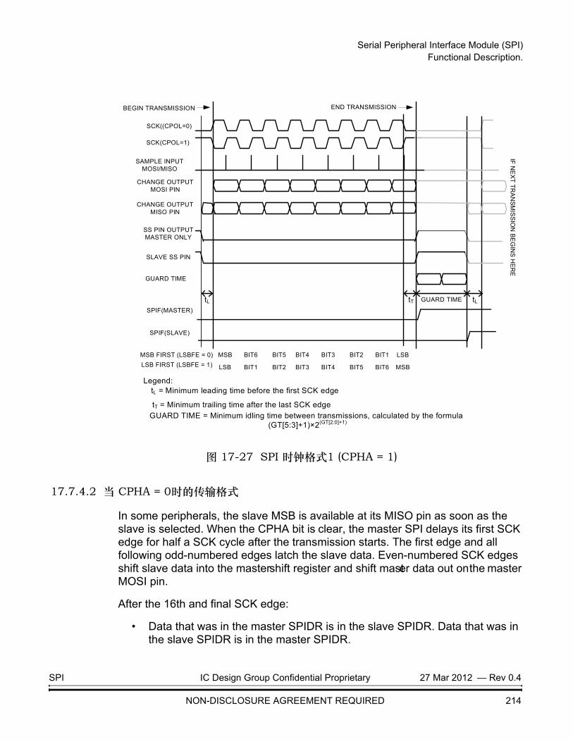
Serial Peripheral Interface Module (SPI) Functional Description.
图 17-27 SPI 时钟格式1 (CPHA = 1)
17.7.4.2 当 CPHA = 0时的传输格式
In some peripherals, the slave MSB is available at its MISO pin as soon as the slave is selected. When the CPHA bit is clear, the master SPI delays its first SCK edge for half a SCK cycle after the transmission starts. The first edge and all following odd-numbered edges latch the slave data. Even-numbered SCK edges shift slave data into the master shift register and shift master data out on the master MOSI pin.
After the 16th and final SCK edge:
• Data that was in the master SPIDR is in the slave SPIDR. Data that was in the slave SPIDR is in the master SPIDR.
SCK((CPOL=0)
SCK(CPOL=1)
BEGIN TRANSMISSION
SAMPLE INPUTMOSI/MISO
GUARD TIME
CHANGE OUTPUTMOSI PIN
CHANGE OUTPUT MISO PIN
SS PIN OUTPUTMASTER ONLY
SLAVE SS PIN
END TRANSMISSION
MSB FIRST (LSBFE = 0)LSB FIRST (LSBFE = 1)
MSB BIT6 BIT5 BIT4 BIT3 BIT2 BIT1 LSB
LSB BIT1 BIT2 BIT3 BIT4 BIT5 BIT6 MSB
tL tT GUARD TIME tL
Legend:tL = Minimum leading time before the first SCK edge
tT = Minimum trailing time after the last SCK edge GUARD TIME = Minimum idling time between transmissions, calculated by the formula
(GT[5:3]+1)×2(GT[2:0]+1)
IF NE
XT TRAN
SMISSIO
N BEG
INS H
ERE
SPIF(MASTER)
SPIF(SLAVE)
SPI IC Design Group Confidential Proprietary 27 Mar 2012 — Rev 0.4
NON-DISCLOSURE AGREEMENT REQUIRED 214

Serial Peripheral Interface Module (SPI) Functional Description.
• The SCK clock stops and the SPIF flag in SPISR is set, indicating that the transmission is complete. If the SPIE bit in SPCR1 is set, SPIF generates an interrupt request.
Figure 17-28 shows the timing of a transmission with the CPHA bit clear. The SS pin of the master must be either high or configured as a general-purpose output not affecting the SPI.
When CPHA = 0, the slave SS pin must be negated and reasserted between bytes.
图 17-28 SPI 时钟格式0 (CPHA = 0)
NOTE: Clock skew between the master and slave can cause data to be lost when:
• CPHA = 0, and,
• The baud rate is the SPI clock divided by two, and
SCK((CPOL=0)
SCK(CPOL=1)
BEGIN TRANSMISSION
SAMPLE INPUTMOSI/MISO
GUARD TIME
CHANGE OUTPUTMOSI PIN
CHANGE OUTPUT MISO PIN
SS PIN OUTPUTMASTER ONLY
SLAVE SS PIN
END TRANSMISSION
MSB FIRST (LSBFE = 0)LSB FIRST (LSBFE = 1)
MSB BIT6 BIT5 BIT4 BIT3 BIT2 BIT1 LSB
LSB BIT1 BIT2 BIT3 BIT4 BIT5 BIT6 MSB
tL tT GUARD TIME tL
Legend:tL = Minimum leading time before the first SCK edge
tT = Minimum trailing time after the last SCK edge GUARD TIME = Minimum idling time between transmissions, calculated by the formula
(GT[5:3]+1)×2(GT[2:0]+1)
IF NEX
T TRAN
SM
ISSIO
N BEG
INS H
ERE
SPIF(MASTER)
SPIF(SLAVE)
SPI IC Design Group Confidential Proprietary 27 Mar 2012 — Rev 0.4
NON-DISCLOSURE AGREEMENT REQUIRED 215

Serial Peripheral Interface Module (SPI) Functional Description.
• The master SCK frequency is half the slave SPI clock frequency, and
• Software writes to the slave SPIDR just before the synchronized SS signal goes low.
The synchronized SS signal is synchronized to the SPI clock. Figure 17-29 shows an example with the synchronized SS signal almost a full SPI clock cycle late. While the synchronized SS of the slave is high, writing is allowed even though the SS pin is already low. The write can change the MISO pin while the master is sampling the MISO line. The first bit of the transfer may not be stable when the master samples it, so the byte sent to the master may be corrupted.
图17-29 由主机/从机时钟偏差引起的传输错误
Also, if the slave generates a late write, its state machine may not have time to reset, causing it to incorrectly receive a byte from the master.
This error is most likely when the SCK frequency is half the slave SPI clock frequency. At other baud rates, the SCK skew is no more than one SPI clock, and there is more time between the synchronized SS signal and the first SCK edge. For
SPI IC Design Group Confidential Proprietary 27 Mar 2012 — Rev 0.4
NON-DISCLOSURE AGREEMENT REQUIRED 216

Serial Peripheral Interface Module (SPI) Functional Description.
example, with a SCK frequency one-fourth the slave SPI clock frequency, there are two SPI clocks between the fall of SS and the SCK edge.
As long as another late SPIDR write does not occur, the following bytes to and from the slave are correctly transmitted.
17.7.4.3 Texas Instruments Synchronous Serial Frame Format
In this mode, SCK and SS are forced Low, and the transmit data line SPI Tx is tristated whenever the SSI is idle. Once the bottom entry of the transmit FIFO contains data, SS is pulsed High for one SCK period. The value to be transmitted is also transferred from the transmit FIFO to the serial shift register of the transmit logic. On the next rising edge of SSIClk, the MSB of the 4 to 16-bit data frame is shifted out on the SSITx pin. Likewise, the MSB of the received data is shifted onto the SSIRx pin by the off-chip serial slave device.
Both the SPI and the off-chip serial slave device then clock each data bit into their serial shifter on each falling edge of SCK. The received data is transferred from the serial shifter to the receive FIFO on the first rising edge of SCK after the LSB has been latched.
Figure 17-30 TI single tranfser
Figure 17-31 TI continuous tranfser
SCK
SS
MOSI/MISO
SCK
SS
MOSI/MISO
SPI IC Design Group Confidential Proprietary 27 Mar 2012 — Rev 0.4
NON-DISCLOSURE AGREEMENT REQUIRED 217

Serial Peripheral Interface Module (SPI) Functional Description.
]
17.7.5 SPI 波特率产生
波特率发生器分割SPI时钟以产生不同的SPI波特时钟。SPIBR寄存器中的SPPR[6:4和SPR[2:0]位负责选择SPI时钟因子。
注:
SPPR = 写入SPPR[6:4]位的值
SPR = 写入 SPR[2:0]位的值
只有当SPI处于主模式下并且正在传输时,波特率发生器才是有效的。否则,为了降低IDD电流,该分频器是无效的。
17.7.6 从模式选择输出
The slave-select output feature automatically drives the SS pin low during transmission to select external devices and drives it high during idle to deselect external devices. When SS output is selected, the SS output pin is connected to the SS input pin of the external device.
In master mode only, setting the SSOE bit in SPICR1 and the DDRSP[3] bit in SPIDDR configures the SS pin as a slave-select output.
Setting the SSOE bit disables the mode fault feature.
NOTE: Be careful when using the slave-select output feature in a multimaster system. The mode fault feature is not available for detecting system errors between masters.
17.7.7 Bidirectional Mode
Setting the SPC0 bit in SPICR1 selects bidirectional mode (see Table 17-6). The SPI uses only one data pin for the interface with external device(s). The MSTR bit determines which pin to use. In master mode, the MOSI pin is the master out/master in pin, MOMI. In slave mode, the MISO pin is the slave out/slave in pin, SISO. The MISO pin in master mode and MOSI pin in slave mode are general-purpose I/O pins.
The direction of each data I/O pin depends on its data direction register bit. A pin configured as an output is the output from the shift register. A pin configured as an input is the input to the shift register, and data coming out of the shift register is discarded.
The SCK pin is an output in master mode and an input in slave mode.
SPI时钟因子 SPPR 1+( ) 2 SPR 1+( )×=
SPI IC Design Group Confidential Proprietary 27 Mar 2012 — Rev 0.4
NON-DISCLOSURE AGREEMENT REQUIRED 218
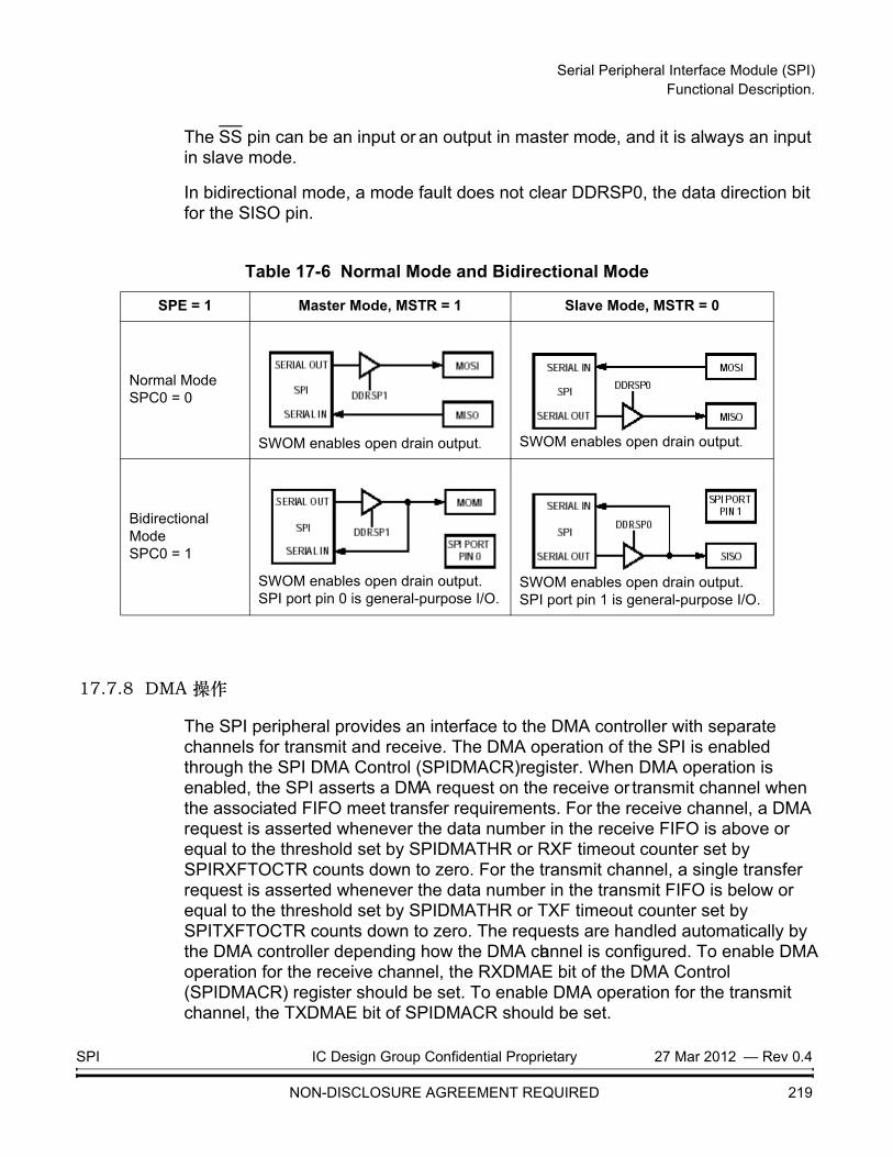
Serial Peripheral Interface Module (SPI) Functional Description.
The SS pin can be an input or an output in master mode, and it is always an input in slave mode.
In bidirectional mode, a mode fault does not clear DDRSP0, the data direction bit for the SISO pin.
17.7.8 DMA 操作
The SPI peripheral provides an interface to the DMA controller with separate channels for transmit and receive. The DMA operation of the SPI is enabled through the SPI DMA Control (SPIDMACR)register. When DMA operation is enabled, the SPI asserts a DMA request on the receive or transmit channel when the associated FIFO meet transfer requirements. For the receive channel, a DMA request is asserted whenever the data number in the receive FIFO is above or equal to the threshold set by SPIDMATHR or RXF timeout counter set by SPIRXFTOCTR counts down to zero. For the transmit channel, a single transfer request is asserted whenever the data number in the transmit FIFO is below or equal to the threshold set by SPIDMATHR or TXF timeout counter set by SPITXFTOCTR counts down to zero. The requests are handled automatically by the DMA controller depending how the DMA channel is configured. To enable DMA operation for the receive channel, the RXDMAE bit of the DMA Control (SPIDMACR) register should be set. To enable DMA operation for the transmit channel, the TXDMAE bit of SPIDMACR should be set.
Table 17-6 Normal Mode and Bidirectional Mode
SPE = 1 Master Mode, MSTR = 1 Slave Mode, MSTR = 0
Normal ModeSPC0 = 0
SWOM enables open drain output. SWOM enables open drain output.
Bidirectional ModeSPC0 = 1
SWOM enables open drain output.SPI port pin 0 is general-purpose I/O.
SWOM enables open drain output.SPI port pin 1 is general-purpose I/O.
SPI IC Design Group Confidential Proprietary 27 Mar 2012 — Rev 0.4
NON-DISCLOSURE AGREEMENT REQUIRED 219

Serial Peripheral Interface Module (SPI) Functional Description.
17.7.9 高速模式
In high speed mode, both the master sample later and the slave shift data out earlier in the SCK period than in normal SPI mode to allow for delays in device pads and board traces. These delays become a more significant fraction of the SCK period as the SCK period decreases with increasing baud rates.
For the master,the high speed mode is enabled by HS bit in SPIURD register when configed as a master and the sample point delay is set by the MSPD[1:0] in SPIPURD register.
For the slave,the high speed mode is enabled by HS bit in SPIURD register when configed as a slave. If HS is set, SPI slave will shift out data at shift-in data edge while the shift-in data timing is the same as normal mode.
For the high speed mode to operate correctly, you must thoroughly analyze the SPI link timing budget.
图 17-32 高速模式 (CPHA = 0)
SCK((CPOL=0)
SCK(CPOL=1)
BEGIN TRANSMISSION
MASTER SAMPLE MISO
GUARD TIME
MASTER OUTPUTMOSI PIN
SLAVE OUTPUT MISO PIN
SS PIN OUTPUTMASTER ONLY
SLAVE SS PIN
END TRANSMISSION
MSB FIRST (LSBFE = 0)LSB FIRST (LSBFE = 1)
MSB BIT6 BIT5 BIT4 BIT3 BIT2 BIT1 LSB
LSB BIT1 BIT2 BIT3 BIT4 BIT5 BIT6 MSB
tL tT GUARD TIME tL
IFN
EXT
TRA
NS
MISS
ION
BEG
INS
HE
RE
SLAVE SAMPLE MOSI
SPI IC Design Group Confidential Proprietary 27 Mar 2012 — Rev 0.4
NON-DISCLOSURE AGREEMENT REQUIRED 220

Serial Peripheral Interface Module (SPI) Reset
17.7.10 低功耗模式操作
本小节介绍低功耗模式的操作。
17.7.10.1 运行模式
清除SPICR1寄存器的SPE位会使SPI处于禁止的,低功耗状态。SPI寄存器是可访问的,但SPI时钟被禁用。
17.7.10.2 休眠模式
在休眠模式下的SPI操作取决于SPICR2寄存器SPISDOZ位的状态。
• 如果清除了SPISDOZ位,在休眠模式下的SPI操作正常。
• 如果SPISDOZ置位了,在休眠模式下SPI时钟停止,并且SPI进入低功耗模 式。
– Any master transmission in progress stops at doze mode entry and resumes at doze mode exit.
– Any slave transmission in progress continues if a master continues to drive the slave SCK pin. The slave stays synchronized to the master SCK clock.
NOTE: Although the slave shift register can receive MOSI data, it cannot transfer data to SPIDR or set the SPIF flag in doze or stop mode. If the slave enters doze mode in an idle state and exits doze mode in an idle state, SPIF remains clear and no transfer to SPIDR occurs.
17.7.10.3 停止模式
SPI进入停止模式与进入休眠模式的方法是一样的,置位SPISDOZ就行。
17.8 复位
Reset initializes the SPI registers to a known startup state as described in 17.6 Memory Map and Registers. A transmission from a slave after reset and before writing to the SPIDR register is either indeterminate or the byte last received from the master before the reset. Reading the SPIDR after reset returns 0s.
SPI IC Design Group Confidential Proprietary 27 Mar 2012 — Rev 0.4
NON-DISCLOSURE AGREEMENT REQUIRED 221

Serial Peripheral Interface Module (SPI) Interrupts
17.9 中断
17.9.1 模式错误(MODF)标志
当主机SPI的SS引脚被拉低,并且SS引脚配置为模式错误输入,那么MODF就被置位。如果MODFIE位也被置位了,MODF就会产生一个中断请求。模式错误可以清除SPE, MSTR和DDRSP[2:0]位。Clear MODF by reading SPISR with MODF set and then writing to SPICR1.
17.9.2 EOT 中断标志 (EOTF)
当所有TX FIFO里的数据都传输完了,EOTF就会被置位。如果SPIE位也被置位了,那么EOTF会产生一个中断请求。通过往该位写1或者由CPU和DMA填充TX FIFO都会清除EOTF。复位清除EOTF。
17.9.3 帧丢失中断标志(FLOST)
当SPI处于从模式,并且TX FIFO内无有效值,而恰好在这个时候主机要开启一次传输,那么SPI就将最后收到的数据返回给主机,同时FLOST置位。如果FLOSTIE也置位了,FLOST就会产生一个中断请求。往该位写1会清除FLOST。复位清除FLOST。
表 17-7 SPI中断请求源
中断请求 标志 使能位
模式错误 MODF MODFIE
传输完成 EOTF SPIE
帧丢失 FLOST FLOSTIE
TXFIFO 超时 TXFTO TXFTOIE
TXFIFO 溢出 TXFOVF TXFOVIE
TXFIFO 下溢 TXFUDF TXFUDIE
TXFIFO 服务 TXFSER TXFSTHIE
RXFIFO 超时 RXFTO RXFTOIE
RXFIFO 溢出 RXFOVF RXFOVIE
RXFIFO 下溢 RXFUDF RXFUDIE
RXFIFO 复位 RXFSER RXFSTHIE
SPI IC Design Group Confidential Proprietary 27 Mar 2012 — Rev 0.4
NON-DISCLOSURE AGREEMENT REQUIRED 222

Serial Peripheral Interface Module (SPI) Interrupts
17.9.4 TXFIFO超时中断标志 (TXFTO)
一旦TX FIFO不为空,计数器就会启动。如果直到计数器计数到0了,而TX FIFO还没有其他操作,那么TXFTO被置位。 计数器是根据SCK的周期来计数的。往该位写1会清除TXFTO。
17.9.5 TXFIFO溢出中断标志 (TXFOVF)
当数据的写操作试图使TX FIFO的数据个数大于8,那么TXFOVF被置位。往该位写1会清除TXFOVF位。
17.9.6 TXFIFO 下溢中断标志 (TXFUDF)
当数据写操作试图使TX FIFO的数据个数小于0时,TXFUDF会被置位。往该位写1会清除TXFUDF。
17.9.7 TXFIFO 服务中断标志 (TXFSER)
当TX FIFO中的数据数小于或等于SPITXFCR寄存器指定的阈值时,TXFSER会被置位。
17.9.8 RXFIFO 超时中断标志 (RXFTO)
一旦RX FIFO不为空,计数器就会启动。如果直到计数器计数到0了,而RX FIFO还没有其他操作,那么RXFTO被置位。 计数器是根据SCK的周期来计数的。往该位写1会清除RXFTO。
17.9.9 RXFIFO 溢出中断标志 (RXFOVF)
当数据写操作试图使RX FIFO的数据个数大于8时,RXFOVF会被置位。往该位写1会清除RXFOVF。
17.9.10 RXFIFO 下溢中断标志(RXFUDF)
当数据写操作试图使RX FIFO的数据个数小于0时,RXFUDF会置位。往该位写1会清除RXFUDF。
17.9.11 RXFIFO 服务中断标志(RXFSER)
当RX FIFO中的数据数量大于或等于SPIRXFCR寄存器指定的阈值时,RXFSER会被置位。
SPI IC Design Group Confidential Proprietary 27 Mar 2012 — Rev 0.4
NON-DISCLOSURE AGREEMENT REQUIRED 223

Advance Information — SCI
第十八节 串行通信接口模块(SCI)
18.1 介绍
串行通信接口(SCI)允许与外围设备和其他微控制器单元(MCU)进行异步串行通信。
18.2 特性
SCI模块的特性包括:
• 标准标记/空间非归零(NRZ)格式
• 波特率因子是22位数字组成的,包括16位整数和6位小数
• 可编程的7位,8位和9位数据格式
• 可单独启用发射器和接收器
• 接收器和发射器可独立地向中央处理单元发出中断请求
• 可编程的发射器输出极性
• 两个接收器唤醒方法:
– 空闲线路唤醒
– 地址标记唤醒
• 驱动中断操作的8个标志:
– 发射器空
– 传输完成
– 接收器满
– 空闲接收器输入
– 接收器溢出
– 噪声错误
– 帧错误
– 极性错误
• 接收器帧错误检测
• 硬件极性检测
SCI IC Design Group Confidential Proprietary Rev 0.1 — 15 Jan 2013
NON-DISCLOSURE AGREEMENT REQUIRED 224

Serial Communications Interface Module (SCI) Modes of Operation
• 1 / 16位时间噪声检测
• 兼容通用I/O口
• 支持红外接口,兼容IrDA协议,最高速度可以到115200bps
18.3 操作模式
• 串行RS-232 NRZ 格式
• IrDA
SCI IC Design Group Confidential Proprietary 15 Jan 2013 — Rev 0.1
NON-DISCLOSURE AGREEMENT REQUIRED 225

Serial Communications Interface Module (SCI) Block Diagram
18.4 框图
图18-1 SCI结构框图
SBRDI[15:0]/SBRDF[5:0]
IRDR
IR Decoder
IR Encoder
SCI IC Design Group Confidential Proprietary 15 Jan 2013 — Rev 0.1
NON-DISCLOSURE AGREEMENT REQUIRED 226

Serial Communications Interface Module (SCI) Modes of Operation
18.5 操作模式
在运行、特殊和调试模式下,SCI的操作是相同的。SCI有两个低功耗模式,分别是休眠模式和停止模式。
说明: 运行模式是正常的操作模式,并且WAIT指令影响SCI的操作。
18.5.1 休眠模式
当SCI上拉与降低驱动寄存器(SCIPURD)中的SCIDOZ位被置位时,DOZE指令会停止SCI时钟并且驱使SCI进入低功耗模式。DOZE指令不会影响SCI的寄存器状态。进入休眠模式时,任何的正在进行的发送和接收操作都会停止。当内部或者外部的中断请求使得CPU退出休眠模式后,发送和接收操作会恢复正常。复位终止任何正在进行的发送或接收和重置SCI, 将退出休眠模式。 详情请参考18.7.7 SCI 数据方向寄存器。
当SCIDOZ位被清除了,DOZE指令的执行对SCI没有任何影响。正常模块操作继续进行,允许任何的SCI中断使CPU退出休眠模式。
18.5.2 停止模式
STOP指令停止SCI时钟并且驱使SCI进入低功耗模式。STOP指令不影响SCI寄存器的状态。进入停止模式时,任何的发送和接收都会停止,当外部中断请求驱动CPU退出停止模式时发送和接收都恢复正常。 复位终止任何正在进行的发送或接收和重置SCI, 将退出休眠模式。
SCI IC Design Group Confidential Proprietary 15 Jan 2013 — Rev 0.1
NON-DISCLOSURE AGREEMENT REQUIRED 227

Serial Communications Interface Module (SCI) Signal Description
18.6 信号描述
表18-1给出了这里的信号的概述
18.6.1 RXD
RXD 是SCI接收引脚。当RXD没有配置成接收器操作时,该引脚为通用I/O口。
18.6.2 TXD
TXD 是SCI发送引脚。当TXD没有配置成发生器操作时,该引脚为通用I/O口。
表18-1 信号属性
名称 功能 端口 复位状态默认上拉 状态
RXD 接收数据引脚 SCIPORT0 0 禁止
TXD 发送数据引脚 SCIPORT1 0 禁止
SCI IC Design Group Confidential Proprietary 15 Jan 2013 — Rev 0.1
NON-DISCLOSURE AGREEMENT REQUIRED 228

Serial Communications Interface Module (SCI) Memory Map and Registers
0x0005
18.7 内存映射与寄存器
SCI的内存映射如表 18-2所示。
说明: 读未定义的地址(0x0000_000f)返回0。写未定义的地址没有意义。访问的未定义的地址不生成错误的响应。
表 18-2 串行通信接口模块内存映射1
SCI1 位 7–0 Access2
0x0003
SCI 控制寄存器2 (SCICR2) S/U
0x0002
SCI 控制寄存器1 (SCICR1) S/U0x0001
SCI 整数波特率因子寄存器低位 (SCIBRDIL) S/U
0x0000
SCI 整数波特率因子寄存器高位(SCIBRDIH) S/U
0x0007
SCI 数据寄存器低位 (SCIDRL) S/U
0x0006
SCI 数据寄存器高位(SCIDRH) S/U
SCI 状态寄存器2 (SCISR2) S/U
0x0004
SCI 状态寄存器1 (SCISR1) S/U
0x000b
SCI 小数波特率因子寄存器(SCIBRDF) S/U
0x000a
SCI 数据方向寄存器 (SCIDDR) S/U0x0009
SCI 端口数据寄存器 (SCIPORT) S/U
0x0008
SCI 上拉与降低驱动寄存器(SCIPURD) S/U
0x000f
保留3 S/U
0x000e
SCI 红外因子寄存器 (SCIIRDR) S/U0x000d
SCI 红外控制寄存器 (SCIIRCR) S/U
0x000c
SCI 测试寄存器(SCITR) S/U
NOTES:
1. Each module is assigned 64 Kbytes of address space, all of which may not be decoded. Accesses outside of the specified module memory map generate a bus error exception.
2. S/U = CPU supervisor or user mode access. User mode accesses to supervisor only addresses have no effect and result in a cycle termination transfer error.
SCI IC Design Group Confidential Proprietary 15 Jan 2013 — Rev 0.1
NON-DISCLOSURE AGREEMENT REQUIRED 229

Serial Communications Interface Module (SCI) Memory Map and Registers
3. Within the specified module memory map, accessing reserved addresses does not generate a bus error exception. Reads of reserved addresses return 0s and writes have no effect.
SCI IC Design Group Confidential Proprietary 15 Jan 2013 — Rev 0.1
NON-DISCLOSURE AGREEMENT REQUIRED 230

Serial Communications Interface Module (SCI) Memory Map and Registers
18.7.1 SCI 控制寄存器 2
图 18-2 SCI 控制寄存器 2 (SCICR2)
读:任何时候
写:任何时候
TIE — 发送中断使能位该可读写位允许TDRE标志产生中断请求。 复位可清除TIE。
1 = TDRE 中断请求使能0 = TDRE 中断请求禁止
TCIE — 传输完成中断使能位该可读写位允许TC标志产生中断请求。复位清除TCIE。
1 = TC 中断请求使能0 = TC 中断请求禁止
RIE — 接收器中断使能位该可读写位允许RDRF 和 OR标志产生中断请求。 复位可清除RIE。
1 = RDRF 和OR中断请求使能0 = RDRF 和OR中断请求禁止
ILIE — 空闲线中断使能位该可读写位允许IDLE标志产生中断请求。 复位可清除ILIE。
1 = IDLE 中断请求使能0 = IDLE 中断请求禁止
TE — 发射器使能位该可读写位使能发射器,并且配置TXD引脚为发射器的输出脚。Toggling TEqueues an idle frame.复位可清除TE。
地址:SCI1 : 0x0000_0000;
Bit7 6 5 4 3 2 1 Bit0Read:
TIE TCIE RIE ILIE TE RE RWU SBKWrite:
RESET: 0 0 0 0 0 0 0 0
SCI IC Design Group Confidential Proprietary 15 Jan 2013 — Rev 0.1
NON-DISCLOSURE AGREEMENT REQUIRED 231

Serial Communications Interface Module (SCI) Memory Map and Registers
1 = 发射器使能0 = 发射器禁止
RE — 接收器使能位该可读写位使能接收器。复位可清除RE。
1 = 接收器使能0 = 接收器禁止
说明: 当LOOPS = 0并且TE = RE = 1时,不管DDRSC1(TXD)和DDRSC0(RXD)的状态是什么, RXD引脚为输入而TXD 引脚为输出。
RWU — 接收器唤醒位该读/写位把接收器处于待机状态,以抑制中断请求接收器。该位决定了是否空闲输入或一个地址标记唤醒接收器和清除RWU。复位可清除RWU。
1 = 当RE=1时,接收器处于睡眠状态0 = 当RE=1时,接收器处于唤醒状态
SBK — Send Break BitSetting this read/write bit causes the SCI to send break frames of 10 (M = 0) or 11 (M =1) logic 0s. To send one break frame, set SBK and then clear it before the break frame is finished transmitting. As long as SBK is set, the transmitter continues to send break frames.
1 = Transmitter sends break frames.0 = Transmitter does not send break frames.
SCI IC Design Group Confidential Proprietary 15 Jan 2013 — Rev 0.1
NON-DISCLOSURE AGREEMENT REQUIRED 232
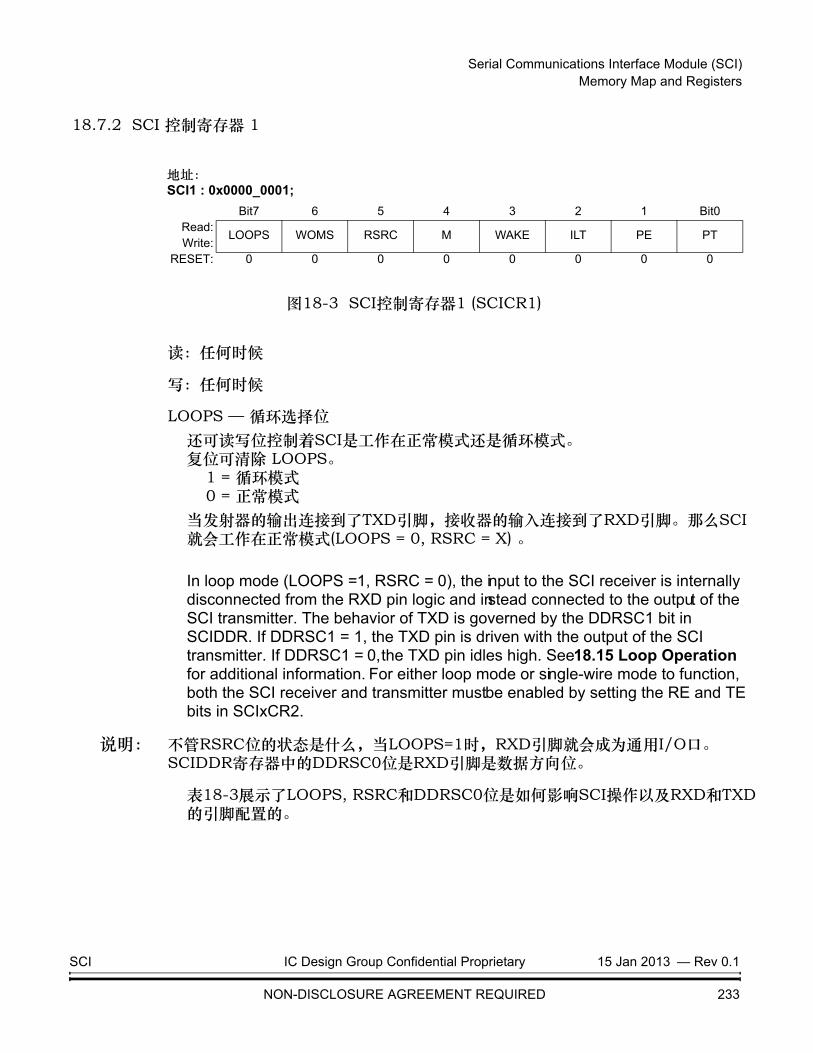
Serial Communications Interface Module (SCI) Memory Map and Registers
18.7.2 SCI 控制寄存器 1
图18-3 SCI控制寄存器1 (SCICR1)
读:任何时候
写:任何时候
LOOPS — 循环选择位还可读写位控制着SCI是工作在正常模式还是循环模式。复位可清除 LOOPS。
1 = 循环模式0 = 正常模式
当发射器的输出连接到了TXD引脚,接收器的输入连接到了RXD引脚。那么SCI就会工作在正常模式(LOOPS = 0, RSRC = X) 。
In loop mode (LOOPS =1, RSRC = 0), the input to the SCI receiver is internally disconnected from the RXD pin logic and instead connected to the output of the SCI transmitter. The behavior of TXD is governed by the DDRSC1 bit in SCIDDR. If DDRSC1 = 1, the TXD pin is driven with the output of the SCI transmitter. If DDRSC1 = 0, the TXD pin idles high. See 18.15 Loop Operation for additional information. For either loop mode or single-wire mode to function, both the SCI receiver and transmitter must be enabled by setting the RE and TE bits in SCIxCR2.
说明: 不管RSRC位的状态是什么,当LOOPS=1时,RXD引脚就会成为通用I/O口。SCIDDR寄存器中的DDRSC0位是RXD引脚是数据方向位。
表18-3展示了LOOPS, RSRC和DDRSC0位是如何影响SCI操作以及RXD和TXD的引脚配置的。
地址: SCI1 : 0x0000_0001;
Bit7 6 5 4 3 2 1 Bit0Read:
LOOPS WOMS RSRC M WAKE ILT PE PTWrite:
RESET: 0 0 0 0 0 0 0 0
SCI IC Design Group Confidential Proprietary 15 Jan 2013 — Rev 0.1
NON-DISCLOSURE AGREEMENT REQUIRED 233

Serial Communications Interface Module (SCI) Memory Map and Registers
WOMS — 线与模式选择位This read/write bit configures the TXD and RXD pins for open-drain operation. This allows all of the TXD pins to be tied together in a multiple-transmitter system. WOMS also affects the TXD and RXD pins when they are general-purpose outputs. External pullup resistors are necessary on open-drain outputs. Reset clears WOMS.
1 = TXD and RXD pins open-drain when outputs0 = TXD and RXD pins CMOS drive when outputs
NOTE: This bit has no effect in this part. Thus wired-or mode is not supported.
RSRC — Receiver Source BitThis read/write bit selects the internal feedback path to the receiver input.Reset clears RSRC. when LOOPS = 1.
1 = Receiver input tied to TXD pin when LOOPS = 10 = Receiver input tied to transmitter output when LOOPS = 1
M — 数据格式位该可读写位选择11位的数据格式还是10位的数据格式。
1 = 1位开始位,9位数据位,1位停止位0 = 1位开始位,8位数据位,1位停止位
WAKE — 唤醒位
表18-3 SCI正常,循环,和单线模式的引脚配置
LOOPS
RSRC
SCI模式 接收器输入RXD引脚
功能
DDRSC0
发射器输出 TXD引脚
功能
0 X 正常 Tied to RXD input buffer 接收引脚 X Tied to TXD output driver 发送引脚
1
0 循环 Tied to transmitter output通用I/O口
0 Tied to receiver input only None (idles high)
1 Tied to receiver input and TXD output driver 发送引脚
1 单线 Tied to TXD0 No connection 接收引脚
1 Tied to TXD output driver 发送引脚
SCI IC Design Group Confidential Proprietary 15 Jan 2013 — Rev 0.1
NON-DISCLOSURE AGREEMENT REQUIRED 234

Serial Communications Interface Module (SCI) Memory Map and Registers
This read/write bit selects the condition that wakes up the SCI receiver when it has been placed in a standby state by setting the RWU bit in SCICR2. When WAKE is set, a logic 1 (address mark) in the most significant bit position of a received data character wakes the receiver. An idle condition on the RXD pin does so when WAKE = 0. Reset clears WAKE.
1 = Address mark receiver wakeup0 = Idle line receiver wakeup
ILT — Idle Line Type BitThis read/write bit determines when the receiver starts counting logic 1s as idle character bits. The counting begins either after the start bit or after the stop bit. If the count begins after the start bit, then a string of logic 1s preceding the stop bit may cause false recognition of an idle character. Beginning the count after the stop bit avoids false idle character recognition, but requires properly synchronized transmissions. Reset clears ILT.
1 = Idle frame bit count begins after stop bit.0 = Idle frame bit count begins after start bit.
PE — Parity Enable BitThis read/write bit enables the parity function. When enabled, the parity function inserts a parity bit in the most significant bit position of an SCI data word. Reset clears PE.
1 = Parity function enabled0 = Parity function disabled
PT — Parity Type BitThis read/write bit selects even parity or odd parity. With even parity, an even number of 1s clears the parity bit and an odd number of 1s sets the parity bit. With odd parity, an odd number of 1s clears the parity bit and an even number of 1s sets the parity bit. Reset clears PT.
1 = Odd parity when PE = 10 = Even parity when PE = 1
SCI IC Design Group Confidential Proprietary 15 Jan 2013 — Rev 0.1
NON-DISCLOSURE AGREEMENT REQUIRED 235

Serial Communications Interface Module (SCI) Memory Map and Registers
18.7.3 SCI 波特率因子寄存器
图18-4 SCI整数波特率因子寄存器高位(SCIBRDIH)
图18-5 SCI整数波特率因子寄存器低位(SCIBRDIL)
图 18-6 SCI小数波特率因子寄存器(SCIBRDF)
读:任何时候
写:任何时候
SBRDI[15:0]— SCI整数波特率因子位
SBRDF[5:0]— SCI小数波特率因子位
地址:SCI1 : 0x0000_0003;
Bit7 6 5 4 3 2 1 Bit0Read:
SBRDI15 SBRDI14 SBRDI13 SBRDI12 SBRDI11 SBRDI10 SBRDI9 SBRDI8Write:
RESET: 0 0 0 0 0 0 0 0
= Writes have no effect and the access terminates without a transfer error exception.
地址: SCI1 : 0x0000_0002;
Bit7 6 5 4 3 2 1 Bit0Read:
SBRDI7 SBRDI6 SBRDI5 SBRDI4 SBRDI3 SBRDI2 SBRDI1 SBRDI0Write:
RESET: 0 0 0 0 0 1 0 0
地址: SCI1 : 0x0000_0008;
Bit7 6 5 4 3 2 1 Bit0Read: 0 0
SBRDF5 SBRDF4 SBRDF3 SBRDF2 SBRDF1 SBRDF0Write:
RESET: 0 0 0 0 0 0 0 0
SCI IC Design Group Confidential Proprietary 15 Jan 2013 — Rev 0.1
NON-DISCLOSURE AGREEMENT REQUIRED 236

Serial Communications Interface Module (SCI) Memory Map and Registers
SBRDI=integer(BRD)=BRDI;
SBRDF=integer(BRDF*64+0.5);
这些课读写位控制着SCI的波特率。
where:
说明: 波特率发生器是禁止的,直到复位后第一时间置位SCICR2寄存器中的TE位和RE位。当SBRDI[15:0]= 0 以及 SBRDF[5:0]=0时,波特率发生器是禁止的。
如果没有同时写SCIBRDL寄存器,写SCIBRDH和SCIBRDF寄存器是没有作用的。写 SCIBRDH和SCIBRDF寄存器会将数据存放在一个临时的位置,直到有数据写入SCIBRDL寄存器中。
BRD BRDI BRDF+ fsys16∗SCIbaudrate-----------------------------------------------= =
SCIbaudrate fsys16∗SBRD---------------------------=
SBRD SBRDI SBRDF64
---------------------+=
1 SBRDI 65536≤ ≤
1 SBRDF 64≤ ≤
SCI IC Design Group Confidential Proprietary 15 Jan 2013 — Rev 0.1
NON-DISCLOSURE AGREEMENT REQUIRED 237
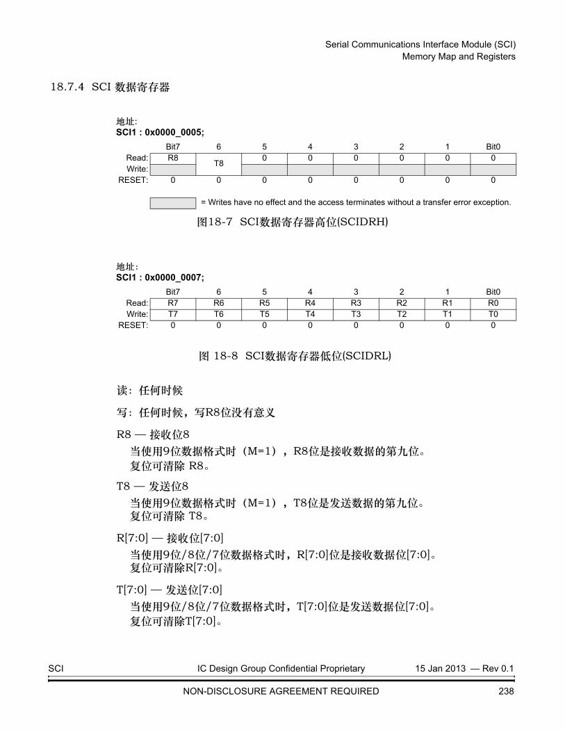
Serial Communications Interface Module (SCI) Memory Map and Registers
18.7.4 SCI 数据寄存器
图18-7 SCI数据寄存器高位(SCIDRH)
图 18-8 SCI数据寄存器低位(SCIDRL)
读:任何时候
写:任何时候,写R8位没有意义
R8 — 接收位8当使用9位数据格式时(M=1),R8位是接收数据的第九位。 复位可清除 R8。
T8 — 发送位8当使用9位数据格式时(M=1),T8位是发送数据的第九位。复位可清除 T8。
R[7:0] — 接收位[7:0]当使用9位/8位/7位数据格式时,R[7:0]位是接收数据位[7:0]。 复位可清除R[7:0]。
T[7:0] — 发送位[7:0]当使用9位/8位/7位数据格式时,T[7:0]位是发送数据位[7:0]。 复位可清除T[7:0]。
地址: SCI1 : 0x0000_0005;
Bit7 6 5 4 3 2 1 Bit0Read: R8
T80 0 0 0 0 0
Write:RESET: 0 0 0 0 0 0 0 0
= Writes have no effect and the access terminates without a transfer error exception.
地址: SCI1 : 0x0000_0007;
Bit7 6 5 4 3 2 1 Bit0Read: R7 R6 R5 R4 R3 R2 R1 R0Write: T7 T6 T5 T4 T3 T2 T1 T0
RESET: 0 0 0 0 0 0 0 0
SCI IC Design Group Confidential Proprietary 15 Jan 2013 — Rev 0.1
NON-DISCLOSURE AGREEMENT REQUIRED 238

Serial Communications Interface Module (SCI) Memory Map and Registers
NOTE: If the value of T8 is the same as in the previous transmission, T8 does not have to be rewritten. The same value is transmitted until T8 is rewritten.
When using the 8-bit data format, only SCIDRL needs to be accessed. When using 8-bit write instructions to transmit 9-bit data, write first to SCIDRH, then to SCIDRL.
18.7.5 SCI 状态寄存器2
图 18-9 SCI 状态寄存器2 (SCISR2)
读:任何时候
写: 任何时候
RAF — 接收器激活标志The RAF flag is set when the receiver detects a logic 0 during the RT1 time period of the start bit search. When the receiver detects an idle character, it clears RAF.Reset clears RAF.
1 = Reception in progress0 = No reception in progress
地址: SCI1 : 0x0000_0006;
Bit7 6 5 4 3 2 1 Bit0Read: 0 0 0 0 0 0 0 RAFWrite:
RESET: 0 0 0 0 0 0 0 0
= Writes have no effect and the access terminates without a transfer error exception.
SCI IC Design Group Confidential Proprietary 15 Jan 2013 — Rev 0.1
NON-DISCLOSURE AGREEMENT REQUIRED 239
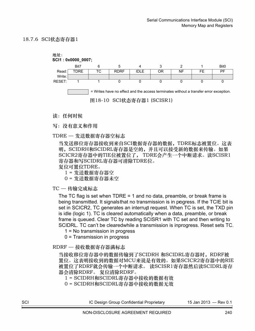
Serial Communications Interface Module (SCI) Memory Map and Registers
18.7.6 SCI状态寄存器1
图18-10 SCI状态寄存器1 (SCISR1)
读:任何时候
写:没有意义和作用
TDRE — 发送数据寄存器空标志当发送移位寄存器接收到来自SCI数据寄存器的数据,TDRE标志被置位。这表明,SCIDRH和SCIDRL寄存器是空的,并且可以接受新的数据来传输。如果SCICR2寄存器中的TIE位被置位了, TDRE会产生一个中断请求。读SCISR1寄存器和写SCIDRL寄存器可清除TDRE位。复位可置位TDRE。
1 = 发送数据寄存器空0 = 发送数据寄存器未空
TC — 传输完成标志The TC flag is set when TDRE = 1 and no data, preamble, or break frame is being transmitted. It signals that no transmission is in progress. If the TCIE bit is set in SCICR2, TC generates an interrupt request. When TC is set, the TXD pin is idle (logic 1). TC is cleared automatically when a data, preamble, or break frame is queued. Clear TC by reading SCISR1 with TC set and then writing to SCIDRL. TC can’t be cleared while a transmission is in progress. Reset sets TC.
1 = No transmission in progress0 = Transmission in progress
RDRF — 接收数据寄存器满标志当接收移位寄存器中的数据传输到了SCIDRH 和SCIDRL寄存器时,RDRF被置位。这表明接收到的数据对MCU来说是有效的。如果SCICR2寄存器中的RIE 被置位了RDRF 就会传输一个中断请求。 读SCISR1寄存器然后读SCIDRL寄存器会清除RDRF。 复位清除RDRF。
1 = SCIDRH和SCIDRL寄存器中接收的数据有效0 = SCIDRH和SCIDRL寄存器中接收的数据无效
地址: SCI1 : 0x0000_0007;
Bit7 6 5 4 3 2 1 Bit0Read: TDRE TC RDRF IDLE OR NF FE PFWrite:
RESET: 1 1 0 0 0 0 0 0
= Writes have no effect and the access terminates without a transfer error exception.
SCI IC Design Group Confidential Proprietary 15 Jan 2013 — Rev 0.1
NON-DISCLOSURE AGREEMENT REQUIRED 240

Serial Communications Interface Module (SCI) Memory Map and Registers
IDLE — Idle Line FlagThe IDLE flag is set when 10 (if M = 0) or 11 (if M = 1) consecutive logic 1s appear on the receiver input. If the ILIE bit in SCICR2 is set, IDLE generates an interrupt request. Once IDLE is cleared, a valid frame must again set the RDRF flag before an idle condition can set the IDLE flag. Clear IDLE by reading SCISR1 and then reading SCIDRL. Reset clears IDLE.
1 = Receiver idle0 = Receiver active or idle since reset or idle since IDLE flag last cleared
NOTE: When RWU of SCICR2 =1, an idle line condition does not set the IDLE flag.
OR — 溢出标志The OR flag is set if data is not read from SCIDRL before the receive shift register receives the stop bit of the next frame. This is a receiver overrun condition. If the RIE bit in SCICR2 is set, OR generates an interrupt request. The data in the shift register is lost, but the data already in the SCIDRH and SCIDRL is not affected. Clear OR by reading SCISR1 and then reading SCIDRL. Reset clears OR.
1 = 溢出0 = 不溢出
NF —噪声标志The NF flag is set when the SCI detects noise on the receiver input. NF is set during the same cycle as the RDRF flag but does not get set in the case of an overrun. Clear NF by reading SCISR1 and then reading SCIDRL. Reset clears NF.
1 =有噪声0 =无噪声
FE — 帧错误标志The FE flag is set when a logic 0 is accepted as the stop bit. FE is set during the same cycle as the RDRF flag but does not get set in the case of an overrun. FE inhibits further data reception until it is cleared. Clear FE by reading SCISR1 and then reading SCIDRL. Reset clears FE.
1 = 出现帧错误0 = 没有帧错误
PF — 奇偶校验错误标志当PE=1,并且接收数据的奇偶校验位与其不匹配时,PF会被置位。读SCISR1寄存器然后读SCIDRL寄存器会清除PF。 复位清除PF。
1 = 出现奇偶检验错误0 = 未出现奇偶检验错误
SCI IC Design Group Confidential Proprietary 15 Jan 2013 — Rev 0.1
NON-DISCLOSURE AGREEMENT REQUIRED 241

Serial Communications Interface Module (SCI) Memory Map and Registers
18.7.7 SCI 数据方向寄存器
图18-11 SCI数据方向寄存器(SCIDDR)
读:任何时候
写:任何时候
RSVD[7:2]— 保留往这些可读写的位写数据会更新它们的值,但在功能上没有任何作用。
DDRSC[1:0] — SCIPORT 数据方向位这些位控制着SCIPORT引脚的数据方向。 复位可清除DDRSC[1:0]。
1 = 相应位配置为输出0 = 相应位配置为输入
说明: 当LOOPS = 0 并且TE = RE = 1时,不管DDRSC1(TXD)和DDRSC0(RXD)位的状态是什么,RXD引脚为输入,TXD引脚为输出。
地址: SCI1 : 0x0000_0009;
Bit7 6 5 4 3 2 1 Bit0Read:
RSVD7 RSVD6 RSVD5 RSVD4 RSVD3 RSVD2 DDRSC1 DDRSC0Write:
RESET: 0 0 0 0 0 0 0 0
SCI IC Design Group Confidential Proprietary 15 Jan 2013 — Rev 0.1
NON-DISCLOSURE AGREEMENT REQUIRED 242

Serial Communications Interface Module (SCI) Memory Map and Registers
18.7.8 SCI 端口数据寄存器
图18-12 SCI端口数据寄存器 (SCIPORT)
读:任何时候;当DDRSCx = 0时,引脚被配置为输入,并且读PORTSCx会返回引脚电平。当 DDRSCx = 1时,引脚被配置为输出,并且读PORTSCx返回的是引脚驱动器输出电平。
写:任何时候;只有当DDRSC位为1,数据储存在内部锁存驱动引脚上。
RSVD[7:2] — 保留这些可读写的位写数据会更新它们的值,但在功能上没有任何作用。
PORTSC[1:0] — SCIPORT 数据位这些是SCI端口的可读写位。
NOTE: 当引脚配置为SCI输入时,写SCIPORT寄存器是不会改变引脚状态的。
To ensure correct reading of the SCI pin values from SCIPORT, always wait at least one cycle after writing to SCIDDR before reading SCIPORT.
地址: SCI1 : 0x0000_000a;
Bit 7 6 5 4 3 2 1 Bit 0Read:
RSVD7 RSVD6 RSVD5 RSVD4 RSVD3 RSVD2 PORTSC1 PORTSC0Write:
RESET: 0 0 0 0 0 0 0 0Pin function: TXD RXD
SCI IC Design Group Confidential Proprietary 15 Jan 2013 — Rev 0.1
NON-DISCLOSURE AGREEMENT REQUIRED 243

Serial Communications Interface Module (SCI) Memory Map and Registers
18.7.9 SCI 上拉与降低驱动寄存器
图18-13 SCI 上拉与降低驱动寄存器(SCIPURD)
写:任何时候
SCISDOZ — 休眠模式下SCI停止(SCI Stop in Doze Mode Bit)SCISDOZ位禁止休眠模式下的SCI。
1 = 休眠模式下SCI禁止0 = 休眠模式下SCI使能
RSVD[5,4,1] — 保留这些可读写的位写数据会更新它们的值,但在功能上没有任何作用。
PUPSCI —上拉使能位该可读写位使能TXD和RXD引脚的上拉。如果引脚被配置为输出,那么上拉会被禁止。
1 = TXD和RXD上拉使能0 = TXD和RXD上拉禁止
NOTE: The PUPSCI bit has no effect in ths part. Pullups are always enabled.
地址: SCI1 : 0x0000_000b;
Bit7 6 5 4 3 2 1 Bit0Read:
SCISDOZ0
RSVD5 RSVD40 0
RSVD1 PUPSCIWrite:
RESET: 0 0 0 0 0 0 0 1
= Writes have no effect and the access terminates without a transfer error exception.
SCI IC Design Group Confidential Proprietary 15 Jan 2013 — Rev 0.1
NON-DISCLOSURE AGREEMENT REQUIRED 244
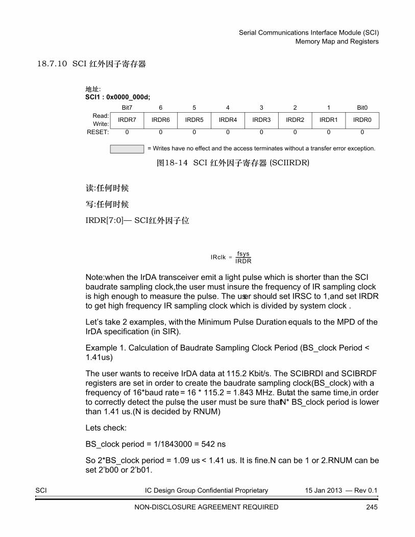
Serial Communications Interface Module (SCI) Memory Map and Registers
18.7.10 SCI 红外因子寄存器
图18-14 SCI 红外因子寄存器 (SCIIRDR)
读:任何时候
写:任何时候
IRDR[7:0]— SCI红外因子位
Note:when the IrDA transceiver emit a light pulse which is shorter than the SCI baudrate sampling clock,the user must insure the frequency of IR sampling clock is high enough to measure the pulse. The user should set IRSC to 1,and set IRDR to get high frequency IR sampling clock which is divided by system clock .
Let’s take 2 examples, with the Minimum Pulse Duration equals to the MPD of the IrDA specification (in SIR).
Example 1. Calculation of Baudrate Sampling Clock Period (BS_clock Period < 1.41us)
The user wants to receive IrDA data at 115.2 Kbit/s. The SCIBRDI and SCIBRDF registers are set in order to create the baudrate sampling clock(BS_clock) with a frequency of 16*baud rate = 16 * 115.2 = 1.843 MHz. But at the same time,in order to correctly detect the pulse, the user must be sure that N* BS_clock period is lower than 1.41 us.(N is decided by RNUM)
Lets check:
BS_clock period = 1/1843000 = 542 ns
So 2*BS_clock period = 1.09 us < 1.41 us. It is fine.N can be 1 or 2.RNUM can be set 2’b00 or 2’b01.
地址: SCI1 : 0x0000_000d;
Bit7 6 5 4 3 2 1 Bit0Read:
IRDR7 IRDR6 IRDR5 IRDR4 IRDR3 IRDR2 IRDR1 IRDR0Write:
RESET: 0 0 0 0 0 0 0 0
= Writes have no effect and the access terminates without a transfer error exception.
IRclk fsysIRDR---------------=
SCI IC Design Group Confidential Proprietary 15 Jan 2013 — Rev 0.1
NON-DISCLOSURE AGREEMENT REQUIRED 245

Serial Communications Interface Module (SCI) Memory Map and Registers
Example 2. Calculation of Baudrate Sampling Clock Period (BS_clock Period > 1.41 us)
This time the user wants to receive at 19.2 Kbit/s. So, the BS_clock is set to 16*19200 = 307.2 kHz.
Let’s check if N* BS_clock period < 1.41 us:
BS_clock period =1/307200 = 3.25 us,
So N*BS_clock period >> 1.41 us. It doesn’t work.
So, in this case, the BS_clock can’t be used to measure the pulse duration and the user must select the IR sampling clock by setting IRSC =1.
When system clock frequency is 32MHz,
SYS_clock period = 1/32000000=0.03125us=IR_clock period/IRDR;
So when N*IR_clock period<1.41us(N<=4),only when IRDR<1.41/(0.03125*N)
when N=1,IRDR set to 8’h2d;IR_clock period=1.406us<1.41us;(N can only be 1)
when N=2,IRDR set to 8’h16;2*IR_clock period=1.375us<1.41us;(N can be 1 or 2)
when N=3,IRDR set to 8’h0f;3*IR_clock period=1.406us<1.41us;(N can be 1 or 2 or 3)
when N=4,IRDR set to 8’h0b;4*IR_clock period=1.375us<1.41us;(N can be 1 or 2 or 3 or 4)
Usually we set RNUM=2’b01(N=2) to sampling pulse.
SCI IC Design Group Confidential Proprietary 15 Jan 2013 — Rev 0.1
NON-DISCLOSURE AGREEMENT REQUIRED 246
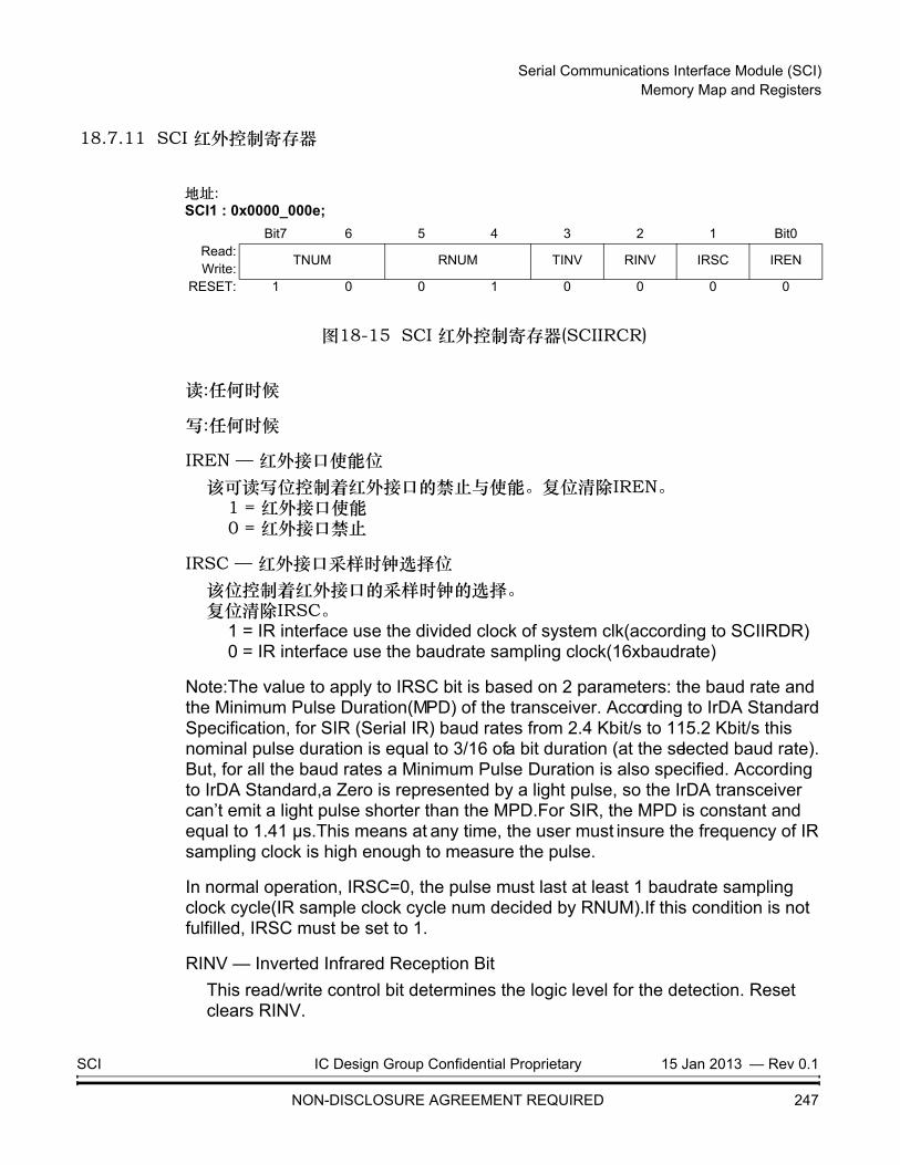
Serial Communications Interface Module (SCI) Memory Map and Registers
18.7.11 SCI 红外控制寄存器
图18-15 SCI 红外控制寄存器(SCIIRCR)
读:任何时候
写:任何时候
IREN — 红外接口使能位该可读写位控制着红外接口的禁止与使能。复位清除IREN。
1 = 红外接口使能0 = 红外接口禁止
IRSC — 红外接口采样时钟选择位该位控制着红外接口的采样时钟的选择。 复位清除IRSC。
1 = IR interface use the divided clock of system clk(according to SCIIRDR)0 = IR interface use the baudrate sampling clock(16xbaudrate)
Note:The value to apply to IRSC bit is based on 2 parameters: the baud rate and the Minimum Pulse Duration(MPD) of the transceiver. According to IrDA Standard Specification, for SIR (Serial IR) baud rates from 2.4 Kbit/s to 115.2 Kbit/s this nominal pulse duration is equal to 3/16 of a bit duration (at the selected baud rate). But, for all the baud rates a Minimum Pulse Duration is also specified. According to IrDA Standard,a Zero is represented by a light pulse, so the IrDA transceiver can’t emit a light pulse shorter than the MPD.For SIR, the MPD is constant and equal to 1.41 µs.This means at any time, the user must insure the frequency of IR sampling clock is high enough to measure the pulse.
In normal operation, IRSC=0, the pulse must last at least 1 baudrate sampling clock cycle(IR sample clock cycle num decided by RNUM).If this condition is not fulfilled, IRSC must be set to 1.
RINV — Inverted Infrared Reception BitThis read/write control bit determines the logic level for the detection. Reset clears RINV.
地址: SCI1 : 0x0000_000e;
Bit7 6 5 4 3 2 1 Bit0Read:
TNUM RNUM TINV RINV IRSC IRENWrite:
RESET: 1 0 0 1 0 0 0 0
SCI IC Design Group Confidential Proprietary 15 Jan 2013 — Rev 0.1
NON-DISCLOSURE AGREEMENT REQUIRED 247

Serial Communications Interface Module (SCI) Memory Map and Registers
1 = Active high detection.The infrared logic block expects an active high or positive IR 3/16 pulse for 0’s and active low are expected for 1’s.
0 = Active low detection.The infrared logic block expects an active low or negative IR 3/16 pulse for 0’s and active high are expected for 1’s.
TINV — Inverted Infrared Transmission BitThis read/write control bit sets the active level for the transmission. Reset clears TINV.
1 = Active low transmission.The infrared logic block transmits an active low or negative IR 3/16 pulse for all 0’s and active high are transmitted for 1’s.
0 = Active high transmission.The infrared logic block transmits an active high or positive IR 3/16 pulse for all 0’s and active low are transmitted for 1’s.
RNUM[1:0] — Reception Number BitThese read/write control bits determines the reception sample numbers for vote logic. Reset value is 2’b01.
Note:The IR sampling clock is determined by IRSC. When set RNUM[1:0]=11,users should set IRSC=1,because according to IrDA spec, 1.41us<MPD<3/16 of a bit duration.If IRSC=0,select BS_CLOCK to sample pulse for 4 times,it’s impossible.
TNUM[1:0] — Transmission Number Bit
This read/write control bit determines the transmission clock cycle numbers for generate pulse. Reset value is 2’b10.
Table 18-4 RNUM[1:0] Sample NUM
00 1 times01 2 times10 3 times11 4 times
Table 18-5 TNUM[1:0] Trans Time
00 1/16 baudrate01 2/16 baudrate10 3/16 baudrate11 reserved
SCI IC Design Group Confidential Proprietary 15 Jan 2013 — Rev 0.1
NON-DISCLOSURE AGREEMENT REQUIRED 248

Serial Communications Interface Module (SCI) Memory Map and Registers
18.7.12 SCI测试寄存器
图18-16 SCI测试寄存器(SCITR)
该寄存器为出厂测试保留。
地址: SCI1 : 0x0000_000f;
Bit7 6 5 4 3 2 1 Bit0Read: 0 0 0 0 0 0 0 0Write:
RESET: 0 0 0 0 0 0 0 0
SCI IC Design Group Confidential Proprietary 15 Jan 2013 — Rev 0.1
NON-DISCLOSURE AGREEMENT REQUIRED 249

Serial Communications Interface Module (SCI) Functional Description
18.8 功能描述
SCI允许MCU与遥控设备(包括其他MCU)之间进行全双工、异步、非归零(NRZ)的串行通信。SCI的发射器和接收器是独立操作的,尽管它们共用一个波特率发生器。CPU监控着SCI的状态,处理将要发生的数据以及接受到的数据。
The SCI module also includes a serial IR (SIR) encoder/decoder block that can be connected to an infrared transceiver to implement an IrDA SIR physical layer.
18.9 数据格式化
SCI使用的是标准NRZ标记/空间数据格式,如图18-17所示。
每一帧都有1位起始位,7/8/9位数据位,以及1位或2位的停止位。清除SCICR1寄存器中的M位会将SCI的数据帧格式配置为10位。置位M位会将SCI的数据帧格式配置为11位。
当SCI被配置为9位数据位时,第9位数据位就是SCI数据寄存器高位(SCIDRH)中的T8位。T8位保持不变,直到传输可被重复使用而无需重写。一个拥有9位数据位的帧的长度是11位。
图18-17 SCI数据格式
18.10 串行红外 (SIR)
The SCI includes an IrDA serial-IR (SIR) encoder/decoder block. The IrDA SIR block provides functionality that converts between an asynchronous data stream and a half-duplex serial SIR interface. No analog processing is performed on-chip. The role of the SIR block is to provide a digital encoded output and decoded input to the SCI. When enabled(IREN=1), the SIR block uses the Tx and Rx pins for the
SCI IC Design Group Confidential Proprietary 15 Jan 2013 — Rev 0.1
NON-DISCLOSURE AGREEMENT REQUIRED 250
Serial Communications Interface Module (SCI) Serial IR (SIR)
SIR protocol. These signals should be connected to an infrared transceiver to implement an IrDA SIR physical layer link. The SIR block can receive and transmit, but it is only half-duplex so it cannot do both at the same time. Transmission must be stopped before data can be received. (The IrDA SIR physical layer specifies a minimum 10-ms delay between transmission and reception.)The Infrared Interface is compatible with IrDA Serial Infrared Physical Layer Specification. In this specification, a “zero” is represented by a positive pulse, and a “one” is represented by no pulse (line remains low).
In the SCI:
In TX: For each “zero” to be transmitted, a narrow positive pulse which is 1/16~3/16 of a bit time is generated(due to TNUM).For each “one” to be transmitted no pulse is generated (output is low). External circuitry has to be provided to drive an Infrared LED.
In RX: When receiving, a narrow negative pulse is expected for each “zero” received while no pulse is expected for each “one” received (input is high).
The values of TINV and RINV depend of the IrDA transceiver connected on the TXD and RXD pins of the SCI.If this transceiver is not inverting on both paths Tx and Rx, a Zero is represented by a positive pulse and a One is represented by no pulse (line remains low).In this case, the bit TINV must be set to 0 and the bit RINV must be set to 1 (because Rx IR block expects an inverted signal).
On the contrary user must set TINV=1 and RINV=0 if both paths of the transceiver are inverting, that is,a Zero is represented as a negative pulse and a One is represented by no pulse (line remains high). The transceiver can also be inverting on only one path (Tx or Rx), in this case TINV and RINV must be together equal to 1 or to 0, depending on which path is inverted.
In Figure 18-18,TINV=0,RINV=0.
While if RINV=1,When receiving, a narrow positive pulse is expected for each “zero” transmitted while no pulse is expected for each “one” transmitted (input is low).
SCI IC Design Group Confidential Proprietary 15 Jan 2013 — Rev 0.1
NON-DISCLOSURE AGREEMENT REQUIRED 251
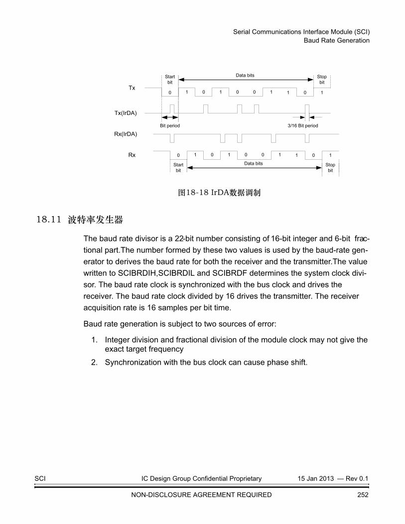
Serial Communications Interface Module (SCI) Baud Rate Generation
图18-18 IrDA数据调制
18.11 波特率发生器
The baud rate divisor is a 22-bit number consisting of 16-bit integer and 6-bit frac-tional part.The number formed by these two values is used by the baud-rate gen-erator to derives the baud rate for both the receiver and the transmitter.The value written to SCIBRDIH,SCIBRDIL and SCIBRDF determines the system clock divi-sor. The baud rate clock is synchronized with the bus clock and drives the receiver. The baud rate clock divided by 16 drives the transmitter. The receiver acquisition rate is 16 samples per bit time.
Baud rate generation is subject to two sources of error:
1. Integer division and fractional division of the module clock may not give the exact target frequency
2. Synchronization with the bus clock can cause phase shift.
Startbit
0 1 0 1 0 0 1 1 0 1
Stopbit
Data bits
Bit period 3/16 Bit period
0 1 0 1 0 0 1 1 0 1
Startbit
Stopbit
Data bits
Tx
Tx(IrDA)
Rx
Rx(IrDA)
SCI IC Design Group Confidential Proprietary 15 Jan 2013 — Rev 0.1
NON-DISCLOSURE AGREEMENT REQUIRED 252

Serial Communications Interface Module (SCI) Baud Rate Generation
Table 18-6 Example Baud Rates (System Clock = 31 MHz)
SBRDI[15:0] SBRDF[5:0] 接收器时钟 (Hz)
发射器时钟(Hz) 目标波特率 错误百分比
0x44cd 0x29 1,760.00 110 110 0.00002%
0x193a 0x15 4,800.00 300.0002 300 0.00008%
0x0c9d 0x0b 9,599.98 599.999 600 0.00016%
0x064e 0x25 19,200.06 1,200.004 1200 0.00032%
0x0327 0x13 38,399.75 2,399.985 2400 0.00065%
0x0193 0x29 76,800.99 4,800.062 4800 0.00129%
0x00c9 0x35 153,596.04 9,599.752 9,600 0.00258%
0x0086 0x23 230,402.97 14,400.19 14,400 0.00129%
0x0064 0x3a 307,215.86 19,200.99 19,200 0.00516%
0x0032 0x1d 614,431.71 38,401.98 38,400 0.00516%
0x0022 0x26 896,115.63 56,007.23 56,000 0.01290%
0x0021 0x29 921,504.88 57,594.05 57,600 0.01032%
0x0010 0x34 1,843,866.17 115,241.6 115,200 0.03614%
0x000f 0x09 2,047,471.62 127,967 128,000 0.02580%
0x0008 0x1a 3,687,732.34 230,483.3 230,400 0.03614%
0x0004 0x000d 7,375,464.68 460,966.5 460,800 0.03614%
0x0001 0x3c 16,000,000.00 1,000,000 1,000,000 0.00000%
0x0000 0x3e 32,000,000.00 2,000,000 2,000,000 0.00000%
SCI IC Design Group Confidential Proprietary 15 Jan 2013 — Rev 0.1
NON-DISCLOSURE AGREEMENT REQUIRED 253
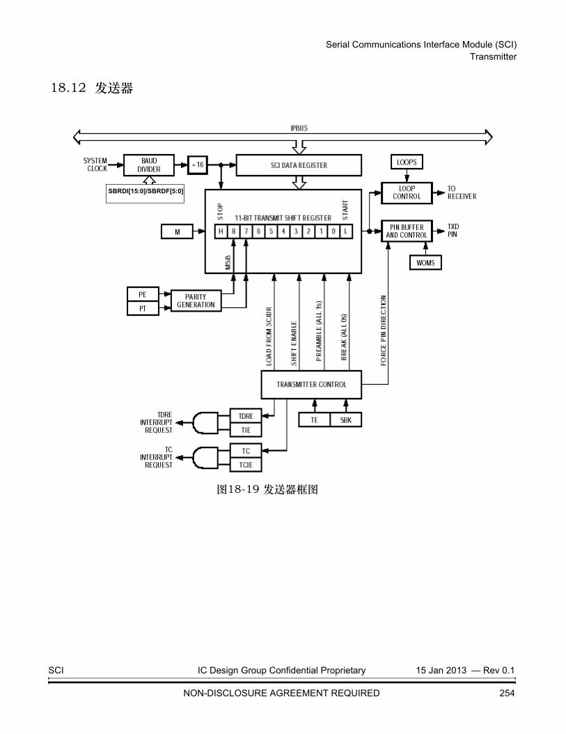
Serial Communications Interface Module (SCI) Transmitter
18.12 发送器
图18-19 发送器框图
SBRDI[15:0]/SBRDF[5:0]
SCI IC Design Group Confidential Proprietary 15 Jan 2013 — Rev 0.1
NON-DISCLOSURE AGREEMENT REQUIRED 254

Serial Communications Interface Module (SCI) Transmitter
18.12.1 帧长度
发生器可以产生10位或者11位长度的帧。在SCICR1寄存器内,M位决定了帧的长度,而PE位使能奇偶校验的功能。 一个数据位可能是一个地址标记或者一个停止位。所有的帧都是从起始位开始,从一位或两位的停止位结束。当传输9位数据时,SCI数据寄存器高位(SCIDRH)中的T8位是第9位(bit 8)。
表18-7 10位和11位帧
M位 帧长 起始位 数据位 奇偶检验位
地址标记
NOTES:
1. When implementing a multidrop network using the SCI, the address mark bit is used to designate subsequent data frames as a network address and not device data.
停止位
0 10位
1 8 No No 1
1 7 No No 2
1 7 No Yes 1
1 7 Yes No 1
1 11位
1 9 No No 1
1 8 No No 2
1 8 No Yes 1
1 8 Yes No 1
1 7 No Yes 2
1 7 Yes No 2
SCI IC Design Group Confidential Proprietary 15 Jan 2013 — Rev 0.1
NON-DISCLOSURE AGREEMENT REQUIRED 255

Serial Communications Interface Module (SCI) Transmitter
18.12.2 发送帧
开始SCI传输的步骤:
1. 配置SCI:
a. 往SCIBDH和SCIBDL寄存器内写入波特率数值。
b. 写 SCICR1寄存器:
i. 启用或禁用循环模式,以及选择接收器的反馈路径
ii. 选择SCI的输出方式:开漏还是线与
iii.选择10位还是11位的帧长
iv. 选择接收器的唤醒条件:地址标记还是空闲线
v. 选择空闲线类型
vi.启用或者禁止奇偶校验功能,以及选择奇校验还是偶校验
c. 写 SCICR2寄存器:
i. 启用或者禁止TDRE, TC, RDRF和IDLE 中断请求
ii. Enable the transmitter and queue a break frame
iii.启用或者禁止接收器
iv. 如果需要,让接收器进入待机
2. 发送一个字节:
a. 读SCISR1寄存器可清除TDRE标志。如果发送的是9位数据,设置SCDRH寄存器的第9位数据位。
b. 将要发送的字节(或者是9位数据的低8位)写入SCIDRL寄存器中。
3. 若多次发送请重复步骤2。
Writing the TE bit from 0 to 1 loads the transmit shift register with a preamble of 10 (if M = 0) or 11 (if M = 1) logic 1s. When the preamble shifts out, the SCI transfers the data from SCIDRH and SCIDRL to the transmit shift register. The transmit shift register prefaces the data with a 0 start bit and appends the data with a 1 stop bit and begins shifting out the frame.
每次从SCIDRH和SCIDRL寄存器中传输数据到发送移位寄存器时,SCI会置位TDRE。TDRE表示SCIDRH和SCIDRL寄存器可以接收新数据。如果TIE位被置位了, TDRE会产生一个中断请求。
NOTE: SCIDRH and SCIDRL transfer data to the transmit shift register and sets TDRE 9/16ths of a bit time after the previous frame’s stop bit starts to shift out.
SCI IC Design Group Confidential Proprietary 15 Jan 2013 — Rev 0.1
NON-DISCLOSURE AGREEMENT REQUIRED 256

Serial Communications Interface Module (SCI) Transmitter
硬件支持奇校验和偶校验。当使能了奇偶校验功能,最重要的数据位就是奇偶校验位。
When the transmit shift register is not transmitting a frame, the TXD pin goes to the idle condition, logic 1. Clearing the TE bit while the transmitter is idle will return control of the TXD pin to the SCI data direction (SCIDDR) and SCI port (SCIPORT) registers.
If the TE bit is cleared while a transmission is in progress (while TC = 0), the frame in the transmit shift register continues to shift out. Then the TXD pin reverts to being a general-purpose I/O pin even if there is data pending in the SCI Data Register. To avoid accidentally cutting off a message, always wait until TDRE is set after the last frame before clearing TE.
To separate messages with preambles with minimum idle line time, use this sequence between messages:
1. Write the last byte of the first message to SCIDRH and SCIDRL.
2. Wait until the TDRE flag is set, indicating the transfer of the last frame to the transmit shift register.
3. Queue a preamble by clearing and then setting the TE bit.
4. Write the first byte of the second message to SCIDRH and SCIDRL.
When the SCI relinquishes the TXD pin, the SCIPORT and SCIDDR registers control the TXD pin.
To force TXD high when turning off the transmitter, set bit 1 of the SCI Port Register (SCIPORT) and bit 1 of the SCI Data Direction Register (SCIDDR). The TXD pin goes high as soon as the SCI relinquishes control of it. See 18.7.7 SCI Data Direction Register and 18.7.7 SCI Data Direction Register
SCI IC Design Group Confidential Proprietary 15 Jan 2013 — Rev 0.1
NON-DISCLOSURE AGREEMENT REQUIRED 257

Serial Communications Interface Module (SCI) Transmitter
18.12.3 Break Frames
Setting the SBK bit in SCICR2 loads the transmit shift register with a break frame. A break frame contains all logic 0s and has no start, stop, or parity bit. Break frame length depends on the M bit in the SCICR1 register. As long as SBK is set, the SCI continuously loads break frames into the transmit shift register. After SBK is clear, the transmit shift register finishes transmitting the last break frame and then transmits at least one logic 1. The automatic logic 1 at the end of a break frame guarantees the recognition of the next start bit.
The SCI recognizes a break frame when a start bit is followed by eight or nine 0 data bits and a 0 where the stop bit should be. Receiving a break frame has these effects on SCI registers:
• Sets the FE flag
• Sets the RDRF flag
• Clears the SCIDRH and SCIDRL
• May set the OR flag, NF flag, PE flag, or the RAF flag
18.12.4 空闲帧
An idle frame contains all logic 1s and has no start, stop, or parity bit. Idle frame length depends on the M bit in the SCICR1 register. The preamble is a synchronizing idle frame that begins the first transmission after writing the TE bit from 0 to 1.
If the TE bit is cleared during a transmission, the TXD pin becomes idle after completion of the transmission in progress. Clearing and then setting the TE bit during a transmission queues an idle frame to be sent after the frame currently being transmitted.
NOTE: When queueing an idle frame, return the TE bit to logic 1 before the stop bit of the current frame shifts out to the TXD pin. Setting TE after the stop bit appears on TXD causesdata previously written to SCIDRH and SCIDRL to be lost. Toggle TE to queue an idle frame, while the TDREflag is set, immediately before writing new data to SCIDRH and SCIDRL.
SCI IC Design Group Confidential Proprietary 15 Jan 2013 — Rev 0.1
NON-DISCLOSURE AGREEMENT REQUIRED 258

Serial Communications Interface Module (SCI) Receiver
18.13 接收器
图18-20 SCI接收器框图
18.13.1 帧长度
接收器可以处理7位、8位或9位数据。SCICR1寄存器内的M位决定了帧的长度。当接收的数据是9位的时候,SCIDRH寄存器中的R8位就是第九位(bit 8)。
18.13.2 接收帧
当SCI接收到数据帧时,该帧就会从RXD引脚转移到接收移位寄存器中。
整个帧都转移进接收移位寄存器中之后,该帧的数据部分会转移到SCIDRH和 SCIDRL寄存器中。RDRF标志置位了,意味着接收到的数据可以被读出。如果
SBRDI[15:0]/SBRDF[5:0]
SCI IC Design Group Confidential Proprietary 15 Jan 2013 — Rev 0.1
NON-DISCLOSURE AGREEMENT REQUIRED 259

Serial Communications Interface Module (SCI) Receiver
RIE位也置位了,RDRF会产生一个中断请求。
18.13.3 数据采样
The receiver samples the RXD pin at the RT clock rate. The RT clock is an internal signal with a frequency 16 times the baud rate. To adjust for baud rate mismatch, the RT clock resynchronizes:
• After every start bit
• After the receiver detects a data bit change from logic 1 to logic 0 (after the majority of data bit samples at RT8, RT9, and RT10 returns a valid logic 1 and the majority of the next RT8, RT9, and RT10 samples returns a valid logic 0)
To locate the start bit, data recovery logic does an asynchronous search for a 0 preceded by three 1s. When the falling edge of a possible start bit occurs, the RT clock begins to count to 16.
图18-21 接收器数据采样
To verify the start bit and to detect noise, data recovery logic takes samples at RT3, RT5, and RT7.
SCI IC Design Group Confidential Proprietary 15 Jan 2013 — Rev 0.1
NON-DISCLOSURE AGREEMENT REQUIRED 260

Serial Communications Interface Module (SCI) Receiver
If start bit verification is not successful, the RT clock is reset and a new search for a start bit begins.
To determine the value of a data bit and to detect noise, recovery logic takes samples at RT8, RT9, and RT10.
NOTE: The RT8, RT9, and RT10 data samples do not affect start bit verification. If any or all of the RT8, RT9, and RT10 samples are logic 1s following a successful start bit verification, the NF flag is set and the receiver interprets the bit as a start bit (logic 0).
The RT8, RT9, and RT10 samples also verify stop bits.
Table 18-8 Start Bit Verification
RT3, RT5, and RT7 Samples Start Bit Verification Noise Flag
000 Yes 0
001 Yes 1
010 Yes 1
011 No 0
100 Yes 1
101 No 0
110 No 0
111 No 0
Table 18-9 Data Bit Recovery
RT8, RT9, and RT10 Samples Data Bit Determination Noise Flag
000 0 0
001 0 1
010 0 1
011 1 1
100 0 1
101 1 1
110 1 1
111 1 0
SCI IC Design Group Confidential Proprietary 15 Jan 2013 — Rev 0.1
NON-DISCLOSURE AGREEMENT REQUIRED 261

Serial Communications Interface Module (SCI) Receiver
In Figure 18-22 the verification samples RT3 and RT5 determine that the first low detected was noise and not the beginning of a start bit. The RT clock is reset and the start bit search begins again. The NF flag is not set because the noise occurred before the start bit was verified.
Figure 18-22 Start Bit Search Example 1
Table 18-10 Stop Bit Recovery
RT8, RT9, and RT10 Samples Framing Error Flag Noise Flag
000 1 0
001 1 1
010 1 1
011 0 1
100 1 1
101 0 1
110 0 1
111 0 0
SCI IC Design Group Confidential Proprietary 15 Jan 2013 — Rev 0.1
NON-DISCLOSURE AGREEMENT REQUIRED 262

Serial Communications Interface Module (SCI) Receiver
In Figure 18-23 noise is perceived as the beginning of a start bit although the RT3 sample is high. The RT3 sample sets the noise flag. Although the perceived bit time is misaligned, the RT8, RT9, and RT10 data samples are within the bit time, and data recovery is successful.
Figure 18-23 Start Bit Search Example 2
In Figure 18-24 a large burst of noise is perceived as the beginning of a start bit, although the RT5 sample is high. The RT5 sample sets the noise flag. Although this is a worst-case misalignment of perceived bit time, the data samples RT8, RT9, and RT10 are within the bit time and data recovery is successful.
Figure 18-24 Start Bit Search Example 3
SCI IC Design Group Confidential Proprietary 15 Jan 2013 — Rev 0.1
NON-DISCLOSURE AGREEMENT REQUIRED 263

Serial Communications Interface Module (SCI) Receiver
Figure 18-25 shows the effect of noise early in the start bit time. Although this noise does not affect proper synchronization with the start bit time, it does set the noise flag.
Figure 18-25 Start Bit Search Example 4
Figure 18-26 shows a burst of noise near the beginning of the start bit that resets the RT clock. The sample after the reset is low but is not preceded by three high samples that would qualify as a falling edge. Depending on the timing of the start bit search and on the data, the frame may be missed entirely or it may set the framing error flag.
Figure 18-26 Start Bit Search Example 5
SCI IC Design Group Confidential Proprietary 15 Jan 2013 — Rev 0.1
NON-DISCLOSURE AGREEMENT REQUIRED 264

Serial Communications Interface Module (SCI) Receiver
In Figure 18-27 a noise burst makes the majority of data samples RT8, RT9, and RT10 high. This sets the noise flag but does not reset the RT clock. In start bits only, the RT8, RT9, and RT10 data samples are ignored.
Figure 18-27 Start Bit Search Example 6
18.13.4 帧错误
If the data recovery logic does not detect a 1 where the stop bit should be in an incoming frame, it sets the FE flag in SCISR1. A break frame also sets the FE flag because a break frame has no stop bit. The FE flag is set at the same time that the RDRF flag is set.
18.13.5 Baud Rate Tolerance
A transmitting device may be operating at a baud rate below or above the receiver baud rate. Accumulated bit time misalignment can cause one of the RT8, RT9, and RT10 stop bit data samples to fall outside the stop bit. A noise error occurs if the samples are not all the same value. If more than one of the samples is outside the stop bit, a framing error occurs. In most applications, the baud rate tolerance is much more than the degree of misalignment that is likely to occur.
As the receiver samples an incoming frame, it resynchronizes the RT clock on any valid falling edge within the frame. Resynchronization within frames corrects misalignments between transmitter bit times and receiver bit times.
SCI IC Design Group Confidential Proprietary 15 Jan 2013 — Rev 0.1
NON-DISCLOSURE AGREEMENT REQUIRED 265

Serial Communications Interface Module (SCI) Receiver
18.13.5.1 Slow Data Tolerance
Figure 18-28 shows how much a slow received frame can be misaligned without causing a noise error or a framing error. The slow stop bit begins at RT8 instead of RT1 but arrives in time for the stop bit data samples at RT8, RT9, and RT10.
Figure 18-28 Slow Data
For 8-bit data, sampling of the stop bit takes the receiver:
With the misaligned data shown in Figure 18-28 ,the receiver counts 154 RT cycles at the point when the count of the transmitting device is:
The maximum percent difference between the receiver count and the transmitter count for slow 8-bit data with no errors is:
For 9-bit data, sampling of the stop bit takes the receiver:
With the misaligned data shown in Figure 18-28, the receiver counts 170 RT cycles at the point when the count of the transmitting device is :
The maximum percent difference between the receiver count and the transmitter count for slow 9-bit data with no errors is:
9 bit times 16 RT cycles× 10 RT cycles 154 RT cycles=+
9 bit times 16 RT cycles× 3 RT cycles 147 RT cycles=+
154 147–154
-------------------------- 100 4.54=× %
10 bit times 16 RT cycles× 10 RT cycles 170 RT cycles=+
10 bit time 16 RT cycles× 3 RT cycles 163 RT cycles=+
170 163–170
-------------------------- 100 4.12=× %
SCI IC Design Group Confidential Proprietary 15 Jan 2013 — Rev 0.1
NON-DISCLOSURE AGREEMENT REQUIRED 266

Serial Communications Interface Module (SCI) Receiver
18.13.5.2 Fast Data Tolerance
Figure 18-29 shows how much a fast received frame can be misaligned without causing a noise error or a framing error. The fast stop bit ends at RT10 instead of RT16 but is still sampled at RT8, RT9, and RT10.
Figure 18-29 Fast Data
For 8-bit data, sampling of the stop bit takes the receiver:
With the misaligned data shown in Figure 18-29 , the receiver counts 154 RT cycles at the point when the count of the transmitting device is:
The maximum percent difference between the receiver count and the transmitter count for fast 8-bit data with no errors is:
For 9-bit data, sampling of the stop bit takes the receiver:
With the misaligned data shown in Figure 18-29, the receiver counts 170 RT cycles at the point when the count of the transmitting device is:
The maximum percent difference between the receiver count and the transmitter count for fast 9-bit data with no errors is:
9 bit times 16 RT cycles× 10 RT cycles 154 RT cycles=+
10 bit times 16RTcycles× 160 RT cycles=
154 160–154
-------------------------- 100 3.90=× %
10 bit times 16 RT cycles× 10 RT cycles 170 RT cycles=+
11 bit times 16RTcycles× 176 RT cycles=
170 176–170
-------------------------- 100 3.53=× %
SCI IC Design Group Confidential Proprietary 15 Jan 2013 — Rev 0.1
NON-DISCLOSURE AGREEMENT REQUIRED 267
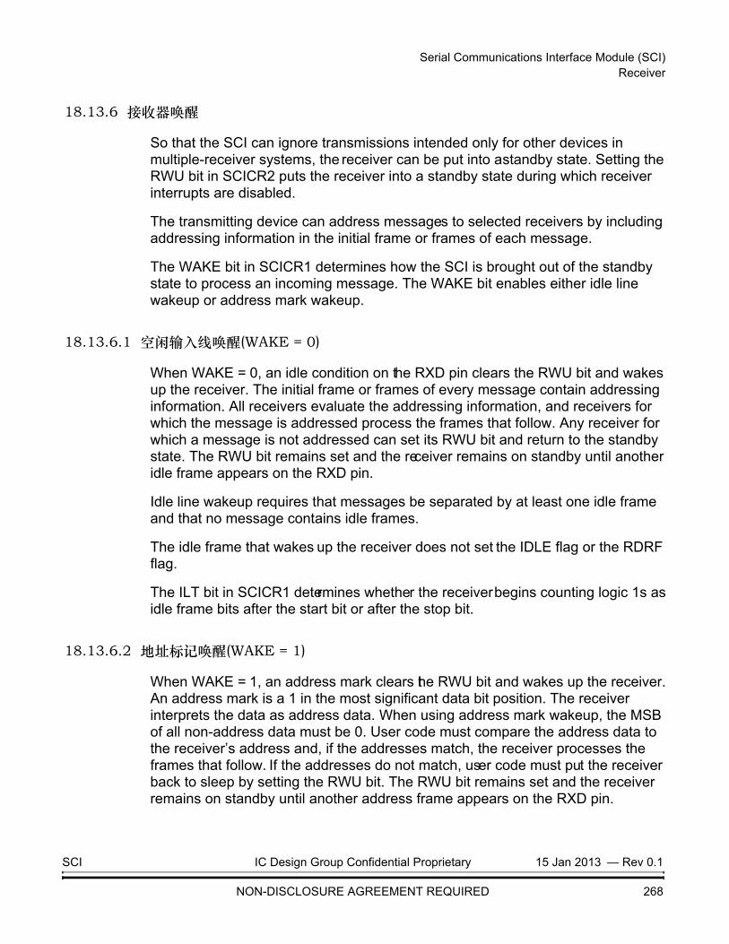
Serial Communications Interface Module (SCI) Receiver
18.13.6 接收器唤醒
So that the SCI can ignore transmissions intended only for other devices in multiple-receiver systems, the receiver can be put into a standby state. Setting the RWU bit in SCICR2 puts the receiver into a standby state during which receiver interrupts are disabled.
The transmitting device can address messages to selected receivers by including addressing information in the initial frame or frames of each message.
The WAKE bit in SCICR1 determines how the SCI is brought out of the standby state to process an incoming message. The WAKE bit enables either idle line wakeup or address mark wakeup.
18.13.6.1 空闲输入线唤醒(WAKE = 0)
When WAKE = 0, an idle condition on the RXD pin clears the RWU bit and wakes up the receiver. The initial frame or frames of every message contain addressing information. All receivers evaluate the addressing information, and receivers for which the message is addressed process the frames that follow. Any receiver for which a message is not addressed can set its RWU bit and return to the standby state. The RWU bit remains set and the receiver remains on standby until another idle frame appears on the RXD pin.
Idle line wakeup requires that messages be separated by at least one idle frame and that no message contains idle frames.
The idle frame that wakes up the receiver does not set the IDLE flag or the RDRF flag.
The ILT bit in SCICR1 determines whether the receiver begins counting logic 1s as idle frame bits after the start bit or after the stop bit.
18.13.6.2 地址标记唤醒(WAKE = 1)
When WAKE = 1, an address mark clears the RWU bit and wakes up the receiver. An address mark is a 1 in the most significant data bit position. The receiver interprets the data as address data. When using address mark wakeup, the MSB of all non-address data must be 0. User code must compare the address data to the receiver’s address and, if the addresses match, the receiver processes the frames that follow. If the addresses do not match, user code must put the receiver back to sleep by setting the RWU bit. The RWU bit remains set and the receiver remains on standby until another address frame appears on the RXD pin.
SCI IC Design Group Confidential Proprietary 15 Jan 2013 — Rev 0.1
NON-DISCLOSURE AGREEMENT REQUIRED 268

Serial Communications Interface Module (SCI) Single-Wire Operation
S
The address mark clears the RWU bit before the stop bit is received and sets the RDRF flag.
Address mark wakeup allows messages to contain idle frames but requires that the most significant byte (MSB) be reserved for address data.
NOTE: With the WAKE bit clear, setting the RWU bit after the RXD pin has been idle can cause the receiver to wake up immediately.
18.14 单线操作
通常,SCI使用TXD引脚用于发送,RXD引脚用于接收(LOOPS = 0, RSRC = X)。但在单线模式下,RXD引脚并没有连接到SCI,而是作为通用I/O口使用。SCI只采用TXD引脚用于发送和接收。
在单线模式下 (LOOPS = 1, RSRC = 1),置位TXD引脚的数据方向位会将TXD引脚配置为发送数据的输出脚。清除TXD引脚的数据方向位会将TXD引脚配置为接收数据的输入脚。
图18-30 单线操作模式(LOOPS = 1, RSRC = 1)
通过置位SCICR1寄存器中的LOOPS位和RSRC位来使能单线操作模式。置位LOOP位意味着切断了RXD引脚到接收器之间的线路。置位RSRC位意味着连接了接收器的输入与TXD引脚驱动器的输出。发射器与接收器必须同时使能 (TE = 1 , RE = 1)。
The WOMS bit in the SCICR1 register configures the TXD pin for full CMOS drive or for open-drain drive. WOMS controls the TXD pin in both normal operation and
SCI IC Design Group Confidential Proprietary 15 Jan 2013 — Rev 0.1
NON-DISCLOSURE AGREEMENT REQUIRED 269

Serial Communications Interface Module (SCI) Loop Operation
)。
in single-wire operation. When WOMS is set, the DDR bit for the TXD pin does not have to be cleared for transmitter to receive data.
18.15 循环模式
在循环模式下(LOOPS = 1, RSRC = 0), 发射器的输出与接收器的输入连接在一起。RXD引脚与SCI断开连接,可作为一个通用I/O引脚。
Setting the DDR bit for the TXD pin connects the transmitter output to the TXD pin. Clearing the data direction bit disconnects the transmitter output from the TXD pin.
图18-31 循环模式(LOOPS = 1, RSRC = 0)
通过置位SCICR1寄存器中的LOOPS位,以及清除RSRC位来使能循环操作模式。 置位LOOPS位意味着切断了RXD引脚到接收器之间的线路。清除RSRC位意味着连接了发射器的输出与接收器的输入。射器与接收器必须同时使能 (TE = 1 , RE = 1
The WOMS bit in SCICR1 configures the TXD pin for full CMOS drive or for open-drain drive. WOMS controls the TXD pin during both normal operation and loop operation.
SCI IC Design Group Confidential Proprietary 15 Jan 2013 — Rev 0.1
NON-DISCLOSURE AGREEMENT REQUIRED 270

Serial Communications Interface Module (SCI) I/O Ports
18.16 I/O 端口
SCIPORT寄存器与两个引脚有关:
• TXD引脚连接到SCIPORT1寄存器。
• RXD引脚连接到SCIPORT0寄存器。
SCI数据方向寄存器(SCIDDR)可将引脚配置为输出或者输入。(详情请参考18.7.7 数据方向寄存器)
18.17 复位
复位初始化SCI 的寄存器为起始状态。详情请参考18.7 内存映射与寄存器。
18.18 中断
下表列出了5个与SCI有关的中断请求。
18.18.1 发送数据寄存器空
当发送移位寄存器接收到来自SCI的数据寄存器的字节时,TDRE会被置位。它表明SCIDRH寄存器和SCIDRL寄存器时空的,并且可以接收新的可以发送的数据。如果SCICR2寄存器中的TIE位也置位了, TDRE会产生一个中断请求。读SCISR1寄存器然后写SCIDRL寄存器可以清除TDRE位。复位可置位TDRE。
表18-11 SCI中断请求源
中断源 标志位 使能位
发射器TDRE TIE
TC TCIE
接收器
RDRF RIE
OR RIE
IDLE ILIE
SCI IC Design Group Confidential Proprietary 15 Jan 2013 — Rev 0.1
NON-DISCLOSURE AGREEMENT REQUIRED 271

Serial Communications Interface Module (SCI) Interrupts
18.18.2 传输完成
The TC flag is set when TDRE = 1 and no data, preamble, or break frame is being transmitted. It signals that no transmission is in progress. If the TCIE bit is set in SCICR2, TC generates an interrupt request. When TC is set, the TXD pin is idle (logic 1). TC is cleared automatically when a data, preamble, or break frame is queued. Clear TC by reading SCISR1 with TC set and then writing to the SCIDRL register. TC cannot be cleared while a transmission is in progress.
18.18.3 接收数据寄存器满
当接收移位寄存器中的数据传输到了SCIDRH寄存器和SCIDRL寄存器中,RDRF会被置位。这意味着接收到的数据可以被读出。如果SCICR2寄存器中的RIE位被置位了,RDRF会产生一个中断请求。读SCISR1寄存器然后读SCIDRL寄存器可以清除RDRF。
18.18.4 空闲接收器输入
The IDLE flag is set when 10 (if M = 0) or 11 (if M = 1) consecutive logic 1s appear on the receiver input. This signals an idle condition on the receiver input. If the ILIE bit in SCICR2 is set, IDLE generates an interrupt request. Once IDLE is cleared, a valid frame must again set the RDRF flag before an idle condition can set the IDLE flag. Clear IDLE by reading SCISR1 with IDLE set and then reading SCIDRL.
18.18.5 溢出
如果在接收移位寄存器接收到下一帧的停止位之前,当前接收的数据都没有从SCIDRL寄存器中读出来,那么OR标志会被置位。这说明接收器溢出了。如果SCICR2寄存器中的RIE位被置位了,那么OR会产生一个中断请求。移位寄存器中的数据会丢失,但已经存在SCIDRH寄存器和SCIDRL寄存器中的数据没有影响。读SCISR1然后读SCIDRL寄存器可以清除OR。
SCI IC Design Group Confidential Proprietary 15 Jan 2013 — Rev 0.1
NON-DISCLOSURE AGREEMENT REQUIRED 272

I2C Introduction
第十九节: I2C
19.1 介绍
I2C是一个双线双向串行总线,它提供了一个数据交换的简单有效的方法,可以最大限度地减少设备之间的互连。该总线适合多台设备间短距离的需要特殊场合通信的应用。灵活的I2C接口允许其他的设备连接到总线以扩展和开发系统。
该总线提供了标准模式下高达100Kbits/s的数据传输速率,快速模式下400Kbits/s的数据传输速率,高速模式下高达3.4Mbits/s的数据传输速率。
The I2C system is a true multiple-master bus including arbitration and collision detection that prevents data corruption if multiple devices attempt to control the bus simultaneously. This feature supports complex applications with multiprocessor control and can be used for rapid testing and alignment of end products through external connections to an assembly-line computer.
19.2 特性
• 支持7位寻址
• 支持标准模式,快速模式和高速模式
• 软件选择高速模式和标准/快速模式
• 与标准和快速I2C总线版本2.1标准兼容.
• 支持多机操作
• 软件可编程的64个不同的串行时钟频率
• 软件可选择的应答位
• Interrupt-driven, byte-by-byte data transfer.
• Arbitration-lost interrupt with automatic mode switching from master to slave.
• 支持传输完成和读配置中断
• 起始和停止信号生成/检测
• Repeated START signal generation.
I2C IC Design Group Confidential Proprietary 27 Mar 2013 — Rev 0.0
NON-DISCLOSURE AGREEMENT REQUIRED 273

I2C
• 应答位生成/检测
• 总线繁忙检测
• Option slave address receiving enable when system clock stop mode
• SCL和SDA可配置为通用I/O口
19.3 系统框图
图 19-1 I2C 框图
19.4 地址映射与寄存器
I2C有5个寄存器,如表19-1所示。
I2C Registers
AddressDecoder
AddrIRQ Data_in Data_out
ClockControl
RX/TXControl&ArbitrationControl
InputSync
sysclk
SDA SCL
In/OutDataShifter
AddressCompare
27 Mar 2013 — Rev 0.0 IC Design Group Confidential Proprietary I2C
274 NON-DISCLOSURE AGREEMENT REQUIRED

I2C Memory Map and Registers
19.4.1 I2C 状态寄存器(I2CS)
I2CS寄存器反映了I2C模块的状态。
TF - 传输完成标志Indicates there is data transmitted or received. For receiver, It is set by the falling edge of the ninth clock of a data(not address) byte received regardless of acknowledge bit detected or not. For master transmitter, It is set by the falling edge of the ninth clock of a data or address byte send regardless of acknowledge bit detected or not. For slave transmitter, it is set by the falling edge of the ninth clock of address or data byte transfered and acknowledge bit must be detected. If the IEN bit in I2CC is also set, an interrupt will be generated. Clear TF by reading I2CS with TF set and then accessing I2CD or master-transmit mode writing I2CC.
表19-1 I2C内存映射地址偏移 位 7- 0
0x0000 I2C状态寄存器 (I2CS)0x0001 I2C时钟预分频器寄存器(I2CP)0x0002 I2C控制寄存器(I2CC)0x0003 I2C从地址寄存器(I2CSA)0x0004 I2C端口控制寄存器(I2CPCR)0x0005 I2C从高速指示寄存器0x0006 I2C从SDA保持时间寄存器0x0007 I2C数据寄存器(I2CD)0x0008 保留0x0009 保留0x000a I2C端口方向寄存器(I2CDDR)0x000b I2C端口数据寄存器(I2CPDR)
地址偏移: 0x0000Bit7 6 5 4 3 2 1 Bit0
Read: AACK DACK RXTX ARBL BBUSY AASLV RC TFWrite:
RESET: 0 0 0 0 0 0 0 0
= Writes have no effect and the access terminates without a transfer error exception.
I2C IC Design Group Confidential Proprietary 27 Mar 2013 — Rev 0.0
NON-DISCLOSURE AGREEMENT REQUIRED 275
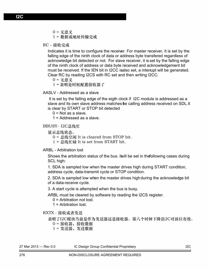
I2C
0 = 无意义1 = 数据或地址传输完成
RC - 接收完成Indicates it is time to configure the receiver. For master receiver, It is set by the falling edge of the ninth clock of data or address byte transfered regardless of acknowledge bit detected or not. For slave receiver, it is set by the falling edge of the ninth clock of address or data byte received and acknowledgement bit must be received. If the IEN bit in I2CC is also set, a interrupt will be generated. Clear RC by reading I2CS with RC set and then writing I2CC.
0 = 无意义1 = 表明是时候配置接收器了
AASLV - Addressed as a slave It is set by the falling edge of the eigth clock if I2C module is addressed as a slave and its own slave address matches the calling address received on SDL.It is clear by START or STOP bit detected
0 = Not as a slave.1 = Addressed as a slave.
BBUSY - I2C总线忙显示总线状态。
0 = 总线空闲 It is cleared from STOP bit.1 = 总线忙碌 It is set from START bit.
ARBL - Arbitration lostShows the arbitration status of the bus. It will be set in the following cases during SCL high: 1. SDA is sampled low when the master drives high during START condition, address cycle, data-transmit cycle or STOP condition. 2. SDA is sampled low when the master drives high during the acknowledge bit of a data-receive cycle.3. A start cycle is attempted when the bus is busy. ARBL must be cleared by software by reading the I2CS register.
0 = Arbitration not lost.1 = Arbitration lost.
RXTX - 接收或者发送表明了I2C模块当前是作为发送器还是接收器。第八个时钟下降沿2C对该位有效。
0 = 接收器,接收数据1 = 发送器,发送数据
27 Mar 2013 — Rev 0.0 IC Design Group Confidential Proprietary I2C
276 NON-DISCLOSURE AGREEMENT REQUIRED

I2C Memory Map and Registers
DACK - 收到数据应答表明在寻址或数据传输过程中是否检测到应答位。 第九个时钟上升沿对该位有效。
0 = 没有收到应答位1 = 收到了应答位
AACK - 地址应答错误Indicates whether the acknowldege bit was detected or not by master during address phase. It is set by the rising edge of ninth clock of the address phase and clear by changing MSMOD from 1 to 0 or repeat start condition.
0 = 未出现地址应答错误1 = 出现了地址应答错误
19.4.2 I2C 时钟分频器寄存器(I2CP)
I2CP is a prescaler to generate a bit-rate clock for the data transceiver. Due to potentially slow SCL and SDA rise and fall times, bus signals are sampled at the prescaler frequency. The serial bit clock frequency is equal to the OPB clock divided by the divider.
PRE[5:0] - 预分频器值
TEST - 时钟测试使能该位使能I2C时钟的测试模式。正常模式下,频率为:fopb/(396x(PRE[5:0]+1)+1);在测试模式下,频率为: fopb/(8x(PRE[5:0]+1)+1).
1 = 时钟测试模式0 = 正常模式
地址偏移: 0x0001Bit7 6 5 4 3 2 1 Bit0
Read: 0TEST PRE5 PRE4 PRE3 PRE2 PRE1 PRE0
Write:RESET: 0 0 0 0 0 0 0 0
= Writes have no effect and the access terminates without a transfer error exception.
I2C IC Design Group Confidential Proprietary 27 Mar 2013 — Rev 0.0
NON-DISCLOSURE AGREEMENT REQUIRED 277

I2C
19.4.3 I2C控制寄存器(I2CC)
I2CC寄存器控制着I2C模块的工作。
EN - I2C允许/禁止被控制1 = 模块使能 0 = 模块禁止
It enables/disables the module. Also controls the software reset of the entire I2C module. Setting the bit generates an internal reset to the module which gets asserted after 2 clock of setting the bit and remain asserted for 3 clocks. Thus reset gets negated after 5 clocks of setting EN bit.If the module is enabled in the middle of a byte transfer, slave mode ignores the current I2C bus transfer and starts operating when the next start condition is detected. Master mode is not aware that the bus is busy; so initiating a start cycle may corrupt the current bus cycle, ultimately causing either the current master or the I2C module to lose arbitration, after which bus operation returns to normal.
IEN - I2C 中断使能控制该位被置位后,I2C的中断会被使能。
1 = I2C 中断使能0 = I2C 中断禁止
MSMOD - I2C 主模式/从模式选择MSMOD从1变化到0时会在总线上产生一个STOP信号,并且选择了从模式。MSMOD从0变化到1时会在总线上产生一个START信号,并且选择了主模式。
1 = 主模式0 = 从模式
ACKEN - 应答使能控制
地址偏移 : 0x0002Bit7 6 5 4 3 2 1 Bit0
Read:SLV_HSIE HMS_EN AMIE REPSTA ACKEN MSMOD IEN EN
Write:RESET: 0 0 0 0 1 0 0 0
= Writes have no effect and the access terminates without a transfer error exception.
27 Mar 2013 — Rev 0.0 IC Design Group Confidential Proprietary I2C
278 NON-DISCLOSURE AGREEMENT REQUIRED

I2C Memory Map and Registers
Specifies the value driven onto SDA during acknowledge cycles for both master and slave receivers. Note that ACKEN bit applies only when the I2C bus receives data byte. During receiving address, if the received address is matched with the slave address, the Acknowledge bit will be sent regardless of the ACKEN bit.
1 = An acknowledge signal is sent to the SDA at the ninth clock bit after receiving one byte of data.
0 = No acknowledge signal is sent to the SDA at the ninth clock bit after receiving one byte of data.
REPSTA - Repeat StartIn these case: 1) The master receiver wasn’t acknowledged after sending slave address or data byte, 2) the master transmitter has send a address or data byte regardless of acknowledged or not , the master can repeat the START signal, followed by a new slave address. The repeat start bit will be send when configure slave address(by writing I2CD) after REPSTA bit set.
1 = Generate repeat start.0 = No repeat start.
AMIE - Address Match Interrupt EnableSelects whether Slave address match will generate interrupt request if I2C interrupt enable control is set to 1. AMIE should be set before entering stop mode to wakeup the system when slave address matched and must be clear when normal work mode.
1 = Enable address match interrupt request.0 = Disable address match interrupt request.
HSM_EN - 高速模式使能
Selects the High Speed mode or Fast/Standard mode operation for the module in master mode. The HSM_EN bit should be set to select the High Speed mode operation. After the transmission of the master code in F/S mode and the HS_I2C does not loose the arbitration, HSM_EN should be set by software, and if you prepare to clear MSMOD to transfer STOP, HSM_EN should be clear by software before after MSMOD.
0 = 快速/标准操作模式(默认)1 = 高速操作模式
SLV_HSIE - 从高速模式中断使能Selects whether Slave High-Speed Mode status will generate interrupt request if 2C interrupt enable control is set to 1.
1 = 允许从高速模式中断0 = 禁止从高速模式中断
I2C IC Design Group Confidential Proprietary 27 Mar 2013 — Rev 0.0
NON-DISCLOSURE AGREEMENT REQUIRED 279

I2C
19.4.4 I2C 从地址寄存器(I2CSA)
当I2C工作在从模式下,并且相应来自主机的地址,I2CSA寄存器就会存储这些地址。
ADDR[7:1] - 模块从地址当I2C模块处于从模式时,该位是从地址。(I2C默认为从模式)
19.4.5 I2C端口控制寄存器(I2CPCR)
SDAPA - SDA端口分配位 该可读写位控制着SDA的功能。
1 = 引脚配置为GPIO0 = 引脚配置为基本功能
SCLPA - SCL端口分配位 该可读写位控制着SCL的功能。
1 = 引脚配置为GPIO0 = 引脚配置为基本功能
WOMI2C[1:0] — 线与模式位该可读写位设置相应的I2C引脚为开漏驱动模式。 WOMI2C[1]控制SDA引脚,WOMI2C[0]控制SCL引脚。这些位只有GPIO模式下是可用的。
1 = 开漏输出0 = CMOS输出
地址偏移 : 0x0003Bit7 6 5 4 3 2 1 Bit0
Read:ADDR7 ADDR6 ADDR5 ADDR4 ADDR3 ADDR2 ADDR1
0Write:
RESET: 0 1 0 0 0 0 0 0
= Writes have no effect and the access terminates without a transfer error exception.
地址偏移: 0x0004Bit7 6 5 4 3 2 1 Bit0
Read:SDAPA SCLPA WOMI2C[1:0] PDI2C[1:0] PUI2C[1:0]
Write:RESET: 0 0 0 0 0 0 1 1
= Writes have no effect and the access terminates without a transfer error exception.
27 Mar 2013 — Rev 0.0 IC Design Group Confidential Proprietary I2C
280 NON-DISCLOSURE AGREEMENT REQUIRED
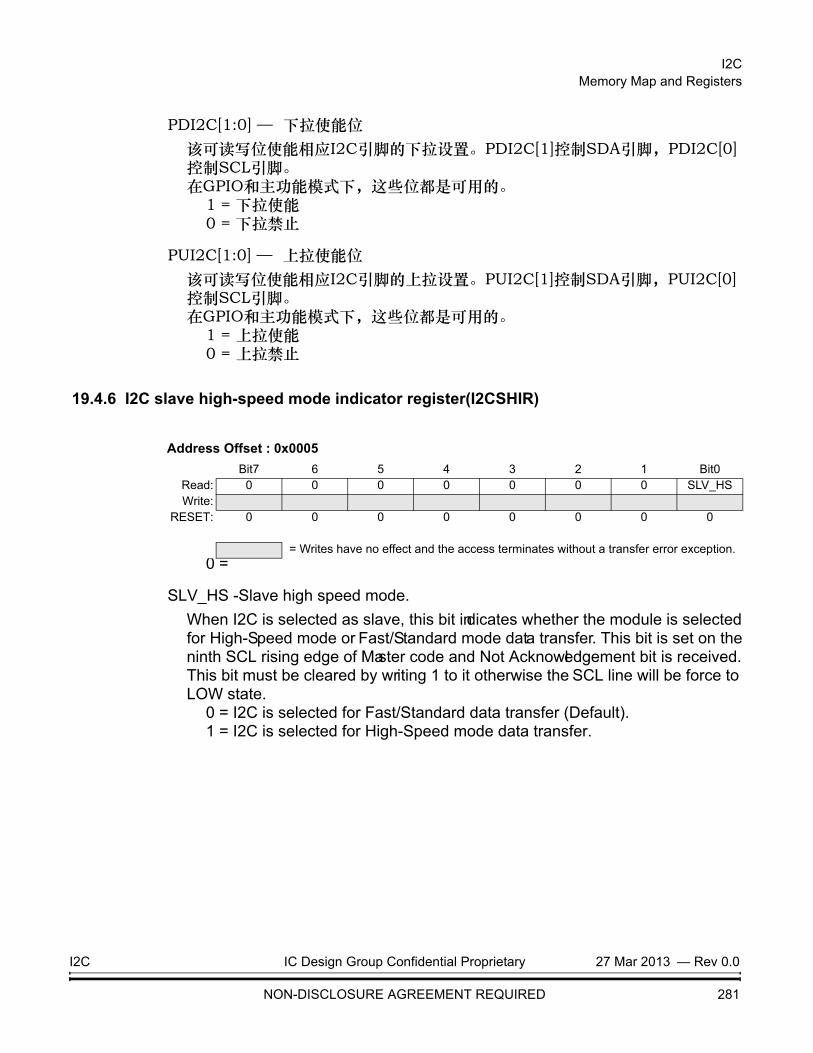
I2C Memory Map and Registers
PDI2C[1:0] — 下拉使能位该可读写位使能相应I2C引脚的下拉设置。PDI2C[1]控制SDA引脚,PDI2C[0]控制SCL引脚。在GPIO和主功能模式下,这些位都是可用的。
1 = 下拉使能0 = 下拉禁止
PUI2C[1:0] — 上拉使能位该可读写位使能相应I2C引脚的上拉设置。PUI2C[1]控制SDA引脚,PUI2C[0]控制SCL引脚。在GPIO和主功能模式下,这些位都是可用的。
1 = 上拉使能0 = 上拉禁止
19.4.6 I2C slave high-speed mode indicator register(I2CSHIR)
0 =
SLV_HS -Slave high speed mode. When I2C is selected as slave, this bit indicates whether the module is selected for High-Speed mode or Fast/Standard mode data transfer. This bit is set on the ninth SCL rising edge of Master code and Not Acknowledgement bit is received. This bit must be cleared by writing 1 to it otherwise the SCL line will be force to LOW state.
0 = I2C is selected for Fast/Standard data transfer (Default).1 = I2C is selected for High-Speed mode data transfer.
Address Offset : 0x0005Bit7 6 5 4 3 2 1 Bit0
Read: 0 0 0 0 0 0 0 SLV_HSWrite:
RESET: 0 0 0 0 0 0 0 0
= Writes have no effect and the access terminates without a transfer error exception.
I2C IC Design Group Confidential Proprietary 27 Mar 2013 — Rev 0.0
NON-DISCLOSURE AGREEMENT REQUIRED 281

I2C
19.4.7 I2C slave SDA hold time register(I2CSHT)
SCL_FILTER_EN - SCL Filter enable.If SCL filter is enabled, when the HS mode transfer is ongoing, the 10ns pulse occured on SCL line will be filter out. If the F/S mode transfer is ongoing, the 50ns pulse occured on SCL line will be filter on.
SDA_FILTER_EN - SDA Filter enable.If SDA filter is enabled, when the HS mode transfer is ongoing, the 10ns pulse occured on SDA line will be filter out. If the F/S mode transfer is ongoing, the 50ns pulse occured on SDA line will be filter on.
SLVHT - slave SDA line hold time configuration.when I2C work as slave output mode, the data will be changed after SCL falling edge and the value of internal SDA hold register equal to SLVHT. Writing value of 0 is not allowed.
19.4.8 I2C 数据寄存器(I2CD)
The I2CD register holds the data to be transmitted (next byte) or data received. In master mode it also holds the slave address and transfer direction to be transmitted. Bits [7:1] form the slave address and bit [0] is the transfer direction (R/W). In master-receiver mode, reading I2CD allows a read to occur and initiates next byte data receiving. In master-transmit mode, writing I2CD will store the byte
Address Offset : 0x0006Bit7 6 5 4 3 2 1 Bit0
Read: SCL_FILTER_EN
SDA_FILTER_EN SLVHT
Write:RESET: 0 0 0 0 1 0 0 1
= Writes have no effect and the access terminates without a transfer error exception.
A地址偏移 : 0x0007Bit7 6 5 4 3 2 1 Bit0
Read: R7 R6 R5 R4 R3 R2 R1 R0Write: T7 T6 T5 T4 T3 T2 T1 T0
RESET: 0 0 0 0 0 0 0 0
= Writes have no effect and the access terminates without a transfer error exception.
27 Mar 2013 — Rev 0.0 IC Design Group Confidential Proprietary I2C
282 NON-DISCLOSURE AGREEMENT REQUIRED

I2C Memory Map and Registers
of the next transmit. In slave mode, the same function is available after it is addressed.
R[7:0] - 接收位[7:0]
T[7:0] - 发送位[7:0]
19.4.9 I2C端口方向寄存器(I2CDDR)
读:任何时候
写:任何时候
DDRI2C[1:0] — I2C数据方向位该可读写位控制着I2C引脚的数据方向。只有在GPIO模式下,这些位才有效。1 = 相应位配置为输出0 = 相应位配置为输入
19.4.10 I2C端口数据寄存器(I2CPDR)
读:任何时候
写:任何时候
PORTI2C[1:0] — I2C 端口数据位
这些位设置已经配置为GPIO口的I2C相应引脚的输出数据。读这些位会返回I2C引脚的电平。
地址偏移: 0x000aBit7 6 5 4 3 2 1 Bit0
Read:Write:
0 0 0 0 0DDRI2C[1:0]
RESET: 0 0 0 0 0 0 0
地址偏移 : 0x000bBit7 6 5 4 3 2 1 Bit0
Read:Write:
0 0 0 0 0 0PORTI2C[1:0]
RESET: 0 0 0 0 0 0 0 0
I2C IC Design Group Confidential Proprietary 27 Mar 2013 — Rev 0.0
NON-DISCLOSURE AGREEMENT REQUIRED 283

I2C
19.5 功能描述
I2C是一个双线双向串行总线,它提供了一个数据交换的简单有效的方法,可以最大限度地减少设备之间的互连。软件可以置位I2C状态标志,或者I2C操作可以中断驱动。当接收或发送一个字节时,I2CS寄存器中的TF位会被置位,,如果I2CC寄存器中的IEN位也被置位了,那么中断就会产生。
If arbitration is lost during it’s transfer, the ARBL will be set and if the IEN bit in I2CC is also set, an interrupt will be generated. An interrupt can also be generated if there is no address acknowledge from the slave (AACK set).
如果模块不希望接收下一字节时,可以清除ACKEN位。
19.5.1 主模式
当I2C是主机时,如果总线是空闲的,那么I2C模块会初始化传输。MSMOD位由0变化到1时,I2C会在总线上产生一个开始信号,并且选择工作模式为主模式。主机控制着传输的方向,即控制着R/W位。主机发送的死一个字节是从机的地址接下来的字节才是数据。MSMOD位由1变化到0时,如果每个时钟的第九位位后仍未收到应答信号,I2C会产生在总线上产生一个停止信号。I2CP寄存器中的PRE[5:0]位控制着I2C总线的时钟比特率。
By configuring slave address after setting the REPSTA bit, the master can repeat the START signal instead of signalling a STOP.
19.5.2 从模式
If the MSMOD bit is cleared the module is a slave and can be addressed by other masters. When a winning master is trying to address it, it will release the SDA line and switch over immediately to its slave mode.
注意: I2C不可以同时工作在主模式和从模式下。
19.5.3 协议
I2C通信协议由7个部分组成:开始位,数据源/宿主位,数据方向位,从机应答位,数据位,数据应答位和停止位。这些位如图19-2所示。
27 Mar 2013 — Rev 0.0 IC Design Group Confidential Proprietary I2C
284 NON-DISCLOSURE AGREEMENT REQUIRED

I2C Functional Description
图 19-2 I2C通信协议
1. START signal—When no other device is bus master (both SCL and SDA lines are at logic high), a device can initiate communication by sending a START signal (see A in Figure 19-2). A START signal is defined as a high-to-low transition of SDA while SCL is high. This signal denotes the beginning of a data transfer (each data transfer can be several bytes long) and awakens all slaves.
2. 从机地址发送—开始信号(B)之后,主机发送的第一个字节就是从机的地址。 7位从机地址发送完毕之后,接着就是一个可读写位R/W(C),该位告知从机数据的传输方向。 每个从机必须拥有一个唯一的地址。I2C主机不允许发送与其从机地址相同的地址。I2C不可以同时为主机和从机。与之机发送的地址匹配的从机会在第九个时钟拉低SDA引脚,以此返回一个应答位。
3. 数据传输—当从机寻址成功完成后, 数据的传输就会根据主机发来的R/W位,以确定的传输方向和逐字传输的方式进行。
只有当SCL是低电平时数据才可以改变,并且在SCL为高电平时要保持稳定。如图 19-2 所示。每来一个SCL脉冲就发送一位数据,并且是先发送MSB位。接收的设备必须在第九个时钟脉冲拉低SDA,以此应答每个字节。因此,一个字节的数据需要九个时钟脉冲。
I2C IC Design Group Confidential Proprietary 27 Mar 2013 — Rev 0.0
NON-DISCLOSURE AGREEMENT REQUIRED 285
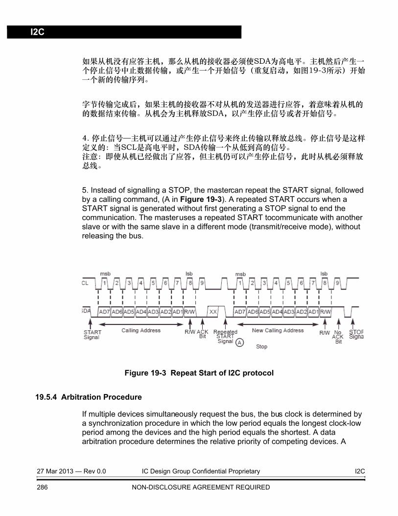
I2C
如果从机没有应答主机,那么从机的接收器必须使SDA为高电平。主机然后产生一个停止信号中止数据传输,或产生一个开始信号(重复启动,如图19-3所示)开始一个新的传输序列。
字节传输完成后,如果主机的接收器不对从机的发送器进行应答,着意味着从机的的数据结束传输。从机会为主机释放SDA,以产生停止信号或者开始信号。
4. 停止信号—主机可以通过产生停止信号来终止传输以释放总线。停止信号是这样定义的:当SCL是高电平时,SDA传输一个从低到高的信号。 注意:即使从机已经做出了应答,但主机仍可以产生停止信号,此时从机必须释放总线。
5. Instead of signalling a STOP, the master can repeat the START signal, followed by a calling command, (A in Figure 19-3). A repeated START occurs when a START signal is generated without first generating a STOP signal to end the communication. The master uses a repeated START to communicate with another slave or with the same slave in a different mode (transmit/receive mode), without releasing the bus.
Figure 19-3 Repeat Start of I2C protocol
19.5.4 Arbitration Procedure
If multiple devices simultaneously request the bus, the bus clock is determined by a synchronization procedure in which the low period equals the longest clock-low period among the devices and the high period equals the shortest. A data arbitration procedure determines the relative priority of competing devices. A
27 Mar 2013 — Rev 0.0 IC Design Group Confidential Proprietary I2C
286 NON-DISCLOSURE AGREEMENT REQUIRED

I2C Functional Description
device loses arbitration if it sends logic high while another sends logic low; it immediately switches to slave-receive mode and stops driving SDA.
A master that loses the arbitration can generate clock pulses until the end of the byte in which it loses the arbitration. It’s possible that the winning master is trying to address it. The losing master must therefore switch over immediately to its slave mode.
In this case, the transition from master to slave mode does not generate a STOP condition. Meanwhile, hardware sets the ARBL bit of I2CSR to indicate loss of arbitration.
19.5.5 时钟同步
Because wired-AND logic is used, a high-to-low transition on SCL affects all devices connected to the bus. Devices start counting their low period when the master drives SCL low. When a device clock goes low, it holds SCL low until the clock high state is reached. However, the low-to-high change in this device clock may not change the state of SCL if another device clock is still in its low period.
Therefore, the device with the longest low period holds the synchronized clock SCL low. Devices with shorter low periods enter a high wait state during this time (See Figure 19-4). When all devices involved have counted off their low period, the synchronized clock SCL is released and pulled high.
There is then no difference between device clocks and the state of SCL, so all of the devices start counting their high periods. The first device to complete its high period pulls SCL low again.
19.5.6 握手
时钟同步机制可以被用作在数据传输中的一次握手。在成功传输一个字节(9位)后,从设备可以保持SCL为低电平。 在这种情况下,时钟机制会停止总线时钟,以及驱使主机时钟进入等待状态,直到从机释放SCL。
19.5.7 Clock Stretching
Slaves can use the clock synchronization mechanism to slow down the transfer bit rate. After the master has driven SCL low, the slave can drive SCL low for the required period and then release it. If the slave SCL low period is longer than the master SCL low period, the resulting SCL bus signal low period is stretched.
I2C IC Design Group Confidential Proprietary 27 Mar 2013 — Rev 0.0
NON-DISCLOSURE AGREEMENT REQUIRED 287

I2C
Figure 19-4 SCL Synchronization
19.5.8 高速模式操作
I2C模块可以在比特率高达3.4Mbits/s的高速模式(HS模式)下传输数据,但它仍然是可以向下兼容具有混合高速总线系统的双向通信设备的快速或标准模式(F/S模式)。With the exception that arbitration and clock synchronization is not performed during the HS-mode transfer, the same serial bus protocol and data format is maintained as with the F/S-mode system.
HS模式下串行数据传送格式符合标准模式的I2C总线规格。HS模式只能在符合下列条件的开始(所有这一切都发生在F / S模式下):
1. START condition (S)
2. 8-bit master code (00001XXX)
3. not-acknowledge bit (A)
更多的细节信息请参考“图19-5 HS模式下的数据传输格式”以及“图19-6 速模式下一个完整的传输”。HS 主机代码有两个主要功能:
1. It allows arbitration and synchronization between competing masters at F/S-mode speeds, resulting in one winning master.
2. It indicates the beginning of an HS-mode transfer.
27 Mar 2013 — Rev 0.0 IC Design Group Confidential Proprietary I2C
288 NON-DISCLOSURE AGREEMENT REQUIRED

I2C Functional Description
HS-mode master codes are reserved 8-bit codes, which are not used for slave addressing or other purposes. Furthermore, as each master has its own unique master code, up to eight HS-mode masters can be present on the one I2C-bus system (although master code 0000 1000 should be reserved for test and diagnostic purposes). The master code for an I2C module is software programmable. Arbitration and clock synchronization only take place during the transmission of the master code and not-acknowledge bit (A), after which one winning master remains active. The master code indicates to other devices that an HS-mode transfer is to begin and the connected devices must meet the HS-mode specification. As no device is allowed to acknowledge the master code, the master code is followed by a not-acknowledge (A). After the not-acknowledge bit (A), and the SCL line has been pulled-up to a HIGH level, the active master switches to HS-mode and enables (at time tH, refer to (see Figure 19-6 A Complet HS mode transfer)) the current-source pull-up circuit for the SCL signal. As other devices can delay the serial transfer before tH by stretching the LOW period of the SCL signal, the active master will enable its current-source pull-up circuit when all devices have released the SCL line and the SCLsignal has reached a HIGH level, thus speeding up the last part of the rise time of the SCL signal. The active master then sends a repeated START condition (Sr)
followed by a 7-bit slave address with a R/W bit address, and receives an acknowledge bit (A) from the selected slave.
After a repeated START condition and after each acknowledge bit (A) or not-acknowledge bit (A), the active master disables its current-source pull-up cir-cuit. This enables other devices to delay the serial transfer by stretching the LOW period of the SCL signal. The active master re-enables its current-sourcepull-up circuit again when all devices have released and the SCL signal reaches a HIGH level, and so speeds up the last part of the SCL signal s rise time.
Data transfer continues in Hs-mode after the next repeated START (Sr), and only switches back to F/S-mode after a STOP condition (P). To reduce the overhead of the master code, it s possible that a master links a number of HS-mode transfers, separated by repeated START conditions (Sr).
I2C IC Design Group Confidential Proprietary 27 Mar 2013 — Rev 0.0
NON-DISCLOSURE AGREEMENT REQUIRED 289

I2C
图19-5 HS模式下的数据传输格式
图19-6 高速模式下一个完整的传输
27 Mar 2013 — Rev 0.0 IC Design Group Confidential Proprietary I2C
290 NON-DISCLOSURE AGREEMENT REQUIRED

I2C Functional Description
19.5.9 软件业务流程图
1. 初始化
置位EN,5个系统时 配置I2CSA钟后,置位IEN, AMIE,ACKEN 和 SLV_HSIE
和 I2CSHT
I2C IC Design Group Confidential Proprietary 27 Mar 2013 — Rev 0.0
NON-DISCLOSURE AGREEMENT REQUIRED 291

I2C
图19-7 从模式初始化
图19-8 主模式初始化
2. 中断处理
置位EN,5个系统时钟 配置I2CSA 和 I2CP
写I2CD寄存器以 配置从机地址 和 R/W
I2C总线 忙?
Yes
No
置位MSMOD以 开始传输
后,置位 IEN 和ACKEN
27 Mar 2013 — Rev 0.0 IC Design Group Confidential Proprietary I2C
292 NON-DISCLOSURE AGREEMENT REQUIRED

I2C Functional Description
图19-9 中断处理
中断 检查 I2CS
AASLV
TF
读I2CD 写I2CC
ARBL
AACK
RC
DACK
重启或 停止
写I2CD寄存器 或停止
重启或 停止
读 I2CD
1
1
1
重启 或停止
清除MSMOD
0
1
0
1
0
1 0
0
1
0
1
0
读 I2CD寄存器
或重启
写I2CD寄存器
DACK
DACK
10
SLV_HS
RC
写 I2CC
0
1
或 HS
AMIE=0
AMIE=0
写I2CSHT寄存器0
1
清除 SLV_HS
TF
AMIE=0
0
I2C IC Design Group Confidential Proprietary 27 Mar 2013 — Rev 0.0
NON-DISCLOSURE AGREEMENT REQUIRED 293

I2C
如果I2C产生了一个中断,首先检查I2CS寄存器,确定I2C是工作在主模式下还是从模式下。
首先检查SLV_HS的状态,如果SLV_HS被置位了,那么就写I2CSHT 寄存器,以 配置高速时序,并且往I2CSHIR寄存器中写1,清除SLV_HS,否则:
在从模式下,如果RC已经被置位了,意味着I2C处于从机接收器模式下,然后检查 TF位,如果TF位同样也已经被置位了,意味着数据(不是地址)已经被接收到了, 然后读I2CD寄存器和写I2CC寄存器以清除RC位和TF位,用来接收下一数据字节。 如果TF还没有被置位,意味着只有从机地址被收到了,然后写I2CC寄存器以清除RC和AMIE,然后接收下一数据字节。在从模式下,如果RC还没有被置位,那么就检查TF位,如果TF位被置位了,那么就检查DACK,如果DACK被置位了,意味着I2C处于从机发送模式,然后写I2CD寄存器清除TF位,写I2CC寄存器清除AMIE,并且发送下一数据字节。如果DACK还没有被置位,那么向I2CD寄存器读出最后接收到的数据,以清除TF。
在从模式下,如果TF和RC都没有被置位,那么写I2CC寄存器以清除AMIE。
In the master mode,if ARBL has been setted,means arbitration lost has been occurred, then write I2CC to clear MSMOD.if ARBL has not been setted then check AACK,if AACK has been setted,means address acknowledge error,then write I2CC to repeat start or stop. 在主模式下,如果ARBL和AACK还没有被置位,那么检查RC,如果RC被置位了, 意味着 I2C处于主机接收器模式下,然后检查DACK,如果DACK也被置位了,那么读I2CD寄存器以清除RC,以及写I2CC寄存器以选择是否应答数据,如果DACK还没被置位,写I2CC寄存器以充分启动或者停止。在主模式下,如果ARBL和AACK还没有被置位,那么检查RC,如果RC没有被置位,意味着I2C处于主机发送器模式下,然后检查DACK,如果DACK已经被置位,写I2CD寄存器以清除TF,并且发送下一数据字节,或者写I2CC寄存器以重复启动或者停止。如果DACK还没被置位,那么写I2CC寄存器以重复启动或停止。
27 Mar 2013 — Rev 0.0 IC Design Group Confidential Proprietary I2C
294 NON-DISCLOSURE AGREEMENT REQUIRED

I2C Functional Description
I2C IC Design Group Confidential Proprietary 27 Mar 2013 — Rev 0.0
NON-DISCLOSURE AGREEMENT REQUIRED 295

I2C
27 Mar 2013 — Rev 0.0 IC Design Group Confidential Proprietary I2C
296 NON-DISCLOSURE AGREEMENT REQUIRED

Advance Information — PWM
第二十节:脉冲宽度调制器 (PWM)
20.1 介绍
There are 4 PWM-Timers enclosed. The 4 PWM-Timers has 2 Pre-scale, 2 clock divider, 4 clock selectors, 4 16-bit counters, 4 16-bit comparators, 2 Dead-Zone generators.Each can be used as a timer and issues interrupt independently.
Each two PWM-Timers share the same pre-scale. Clock divider provides each timer with 5 clock sources (1, 1/2, 1/4, 1/8, 1/16). The 16-bit counter in each timer receive clock signal from clock selector and can be used to handle one PWM period. The 16-bit comparator compares number in counter with threshold number in register loaded previously to generate PWM duty cycle. The clock signal from clock divider is called PWM clock. Dead-Zone generator utilize PWM clock as clock source. Once Dead-Zone generator is enabled, output of two PWM-Timers are blocked. Two output pin are all used as Dead-Zone generator output signal to control off-chip power device. The value of comparator is used for pulse width modulation. The counter control logic changes the output level when down-counter value matches the value of compare register.
Each PWM-Timer includes a capture channel. The Capture 0 and PWM 0 share a timer that included in PWM 0; and the Capture 1 and PWM 1 share another timer, and etc.Therefore user must setup the PWM-Timer before turn on Capture feature. After enabling capture feature, the capture always latched PWM-counter to CRLR when input channel has a rising transition and latched PWM-counter to CFLR when input channel has a falling transition. Capture channel 0 interrupt is programmable by setting CCR0[1] (Rising latch Interrupt enable) and CCR0[2] (Falling latch Interrupt enable) to decide the condition of interrupt occur. Capture channel1&2&3 has the same feature.Whenever Capture issues Interrupt 0/1/2/3, the PWM counter 0/1/2/3 will be reload at this moment. The maximal capture frequency should be decided by interrupt process time.If interrupt precess time is T0,then the capture channel input signal should not change in T0,the maximal capture frequency is 1/T0.
There are only four interrupts from PWM to interrupt controller (INTC). PWM 0 and Capture 0 share the same interrupt; PWM1 and Capture 1 share the same interrupt and so on. Therefore, PWM function and Capture function in the same channel cannot be used at the same time.
PWM IC Design Group Confidential Proprietary Rev 0.1 — 15 Jan 2013
NON-DISCLOSURE AGREEMENT REQUIRED 297

Pulse Width Modulator (PWM)
20.2 特性
脉冲宽度调制器包括这些鲜明的特点:
• 可编程周期
• 可编程占空比
• 两个死区发生器
• 支持捕获功能
• 引脚可配置为通用IO口
15 Jan 2013 — Rev 0.1 IC Design Group Confidential Proprietary PWM
298 NON-DISCLOSURE AGREEMENT REQUIRED
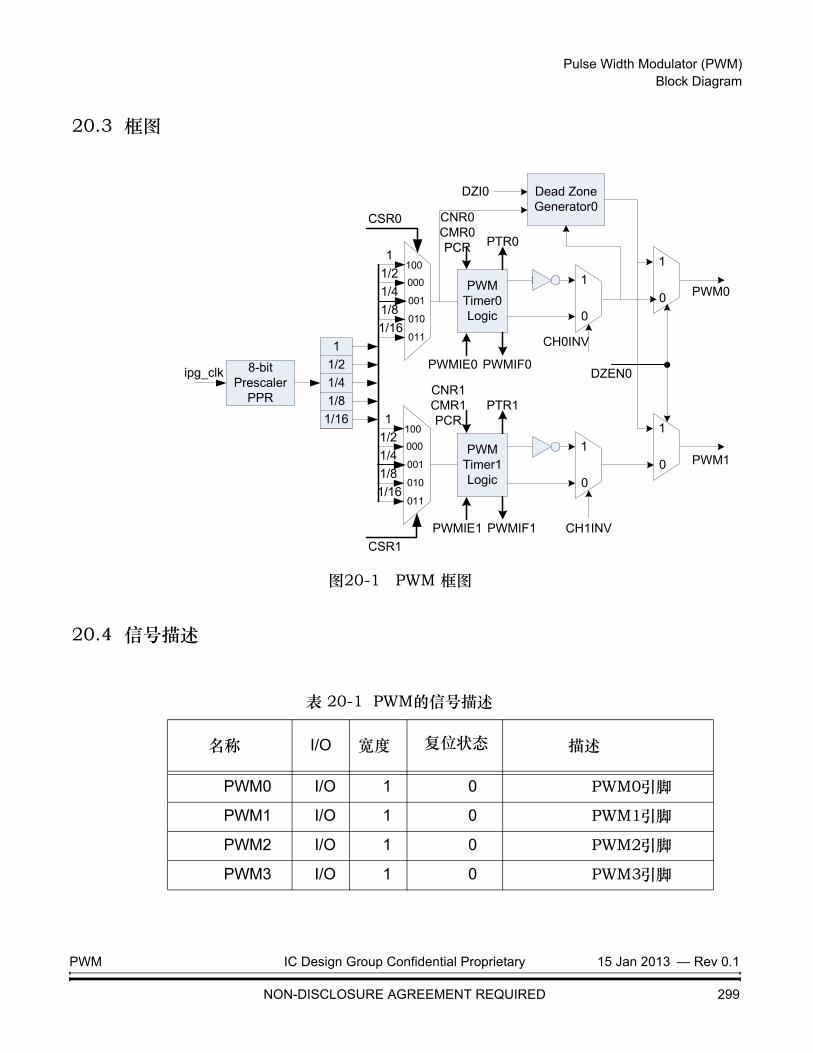
Pulse Width Modulator (PWM) Block Diagram
20.3 框图
图20-1 PWM 框图
20.4 信号描述
11/21/41/8
1/16
100
000
001
010
011
11/21/41/81/16
100
000
001
010
011
11/21/41/81/16
8-bit Prescaler
PPR
ipg_clk
CSR0
CSR1
PWM Timer0 Logic
PWM Timer1 Logic
1
0
1
0
1
0
1
0
Dead ZoneGenerator0
CNR0CMR0PCR PTR0
PWMIE0 PWMIF0
CH0INV
DZEN0
PWM0
PWM1
CH1INV
CNR1CMR1PCR
PTR1
PWMIE1 PWMIF1
DZI0
表 20-1 PWM的信号描述
名称 I/O 宽度 复位状态 描述
PWM0 I/O 1 0 PWM0 引脚
PWM1 I/O 1 0 PWM1 引脚
PWM2 I/O 1 0 PWM2 引脚
PWM3 I/O 1 0 PWM3 引脚
PWM IC Design Group Confidential Proprietary 15 Jan 2013 — Rev 0.1
NON-DISCLOSURE AGREEMENT REQUIRED 299

Pulse Width Modulator (PWM)
PWMx可用作通用的输入/输出引脚,同时可以用作PWM的发送输出或者捕获输入。默认状态下,PWMx用作通用输入口。
15 Jan 2013 — Rev 0.1 IC Design Group Confidential Proprietary PWM
300 NON-DISCLOSURE AGREEMENT REQUIRED

Pulse Width Modulator (PWM) Memory Map and Registers
位 [31:16] 位[15:0]
20.5 内存映射与寄存器
本小节描述了内存映射和寄存器结构。
20.5.1 内存映射
表20-2 模块的内存映射
地址 Access(1)
NOTES:1. S/U = CPU supervisor or user mode access.
0x0000 PWM Pre-scale Register (PPR) S/U0x0004 PWM时钟选择控制器(PCSR) S/U0x0008 PWM控制寄存器(PCR) S/U0x000C PWM计数器寄存器0(PCNR0) S/U0x0010 PWM比较器寄存器0 (PCMR0) S/U0x0014 PWM定时器寄存器0 (PTR0) S/U0x0018 PWM计数器寄存器1(PCNR1) S/U0x001C PWM比较器寄存器1 (PCMR1) S/U0x0020 PWM定时器寄存器1 (PTR1) S/U0x0024 PWM计数器寄存器2 (PCNR2) S/U0x0028 PWM比较器寄存器2 (PCMR2) S/U0x002C PWM定时器寄存器2 (PTR2) S/U0x0030 PWM计数器定时器3 (PCNR3) S/U0x0034 PWM比较器定时器3 (PCMR3) S/U0x0038 PWM定时器寄存器3 (PTR3) S/U0x003C PWM中断使能寄存器(PIER) S/U0x0040 PWM中断标志寄存器 (PIFR) S/U0x0044 PWM捕获控制寄存器0 (PCCR0) S/U0x0048 PWM捕获控制寄存器1 (PCCR1) S/U0x004C PWM捕获上升锁存寄存器0 (PCRLR0) S/U0x0050 PWM捕获下降锁存寄存器0 (PCFLR0) S/U0x0054 PWM捕获上升锁存寄存器1 (PCRLR1) S/U0x0058 PWM捕获下降锁存寄存器1 (PCFLR1) S/U0x005C PWM捕获上升锁存寄存器2 (PCRLR2) S/U0x0060 PWM捕获下降锁存寄存器2 (PCFLR2) S/U0x0064 PWM捕获上升锁存寄存器3 (PCRLR3) S/U0x0068 PWM捕获下降锁存寄存器3 (PCFLR3) S/U0x006C PWM端口控制寄存器(PCR) S/U
PWM IC Design Group Confidential Proprietary 15 Jan 2013 — Rev 0.1
NON-DISCLOSURE AGREEMENT REQUIRED 301

Pulse Width Modulator (PWM)
20.5.2 寄存器
20.5.2.1 PWM预分频寄存器(PPR)
该寄存器(PPR)是用来设置预分频值和死区长度的。
图20-2 PWM预分频寄存器(PPR)
DZI1[7:0] — Dead zone interval register 1 for PWM2 and PWM3 These 8-bit determine dead zone length. The 1 unit time of dead zone length is received from clock selector 1.
DZI0[7:0] — Dead zone interval register 0 for PWM0 and PWM1 These 8-bit determine dead zone length. The 1 unit time of dead zone length is received from clock selector 0.
CP1[7:0] — Clock pre-scale 1 for PWM Timer 2 & 3 Clock input is divided by (CP1 + 1) before it is fed to the counter of PWM Timer 2 & 3.If CP1=0, then the pre-scale 1 output clock will be stopped.
CP0[7:0] — Clock pre-scale 0 for PWM Timer 0 & 1 Clock input is divided by (CP0 + 1) before it is fed to the counter of PWM Timer 0 & 1.If CP0=0, then the pre-scale 0 output clock will be stopped.
地址 : 0x0000和 0x000331 30 29 28 27 26 25 24
RDZI1
WRESET: 0 0 0 0 0 0 0 0
23 22 21 20 19 18 17 16R
DZI0W
RESET: 0 0 0 0 0 0 0 0
15 14 13 12 11 10 9 8R
CP1W
RESET: 0 0 0 0 0 0 0 0
7 6 5 4 3 2 1 0R
CP0W
RESET: 0 0 0 0 0 0 0 0
= Writes have no effect and the access terminates without a transfer error exception.
15 Jan 2013 — Rev 0.1 IC Design Group Confidential Proprietary PWM
302 NON-DISCLOSURE AGREEMENT REQUIRED

Pulse Width Modulator (PWM) Memory Map and Registers
20.5.2.2 PWM时钟选择寄存器(PCSR)
Clock divider provides each timer with 5 clock sources (1, 1/2, 1/4, 1/8, 1/16). Each timer receives its own clock signal from clock divider which receives clock from 8-bit pre-scale.
图20-3 PWM时钟选择寄存器
CSR3[2:0] — 定时器3时钟源选择为定时器3选择时钟输入。
CSR2[2:0] — 定时器2时钟源选择
定时器2的时钟源选择与CSR3相同。
CSR1[2:0] — 定时器1时钟源选择
Address : 0x0004 and 0x000731 30 29 28 27 26 25 24
R 0W
RESET: 0 0 0 0 0 0 0 0
23 22 21 20 19 18 17 16R 0W
RESET: 0 0 0 0 0 0 0 0
15 14 13 12 11 10 9 8R 0
CSR30
CSR2W
RESET: 0 0 0 0 0 0 0 0
7 6 5 4 3 2 1 0R 0
CSR10
CSR0W
RESET: 0 0 0 0 0 0 0 0
= Writes have no effect and the access terminates without a transfer error exception.
表 20-3
CSR3[2:0] 输入时钟分频
100~111 1011 16010 8001 4000 2
PWM IC Design Group Confidential Proprietary 15 Jan 2013 — Rev 0.1
NON-DISCLOSURE AGREEMENT REQUIRED 303

Pulse Width Modulator (PWM)
定时器1的时钟源选择与CSR3相同。
CSR0[2:0] — 定时器0时钟源选择
定时器0的时钟源选择与CSR3相同。
15 Jan 2013 — Rev 0.1 IC Design Group Confidential Proprietary PWM
304 NON-DISCLOSURE AGREEMENT REQUIRED

Pulse Width Modulator (PWM) Memory Map and Registers
20.5.2.3 PWM控制寄存器(PCR)
该寄存器是PWM控制寄存器。
图 20-4 PWM控制寄存器(PCR)
CH3MOD — 定时器3自动重装/单次触发模式1 = 自动重装模式0 = 单次触发模式
注意:如果有一个上升沿或下降沿在该位上转变,那么就会造成CNR3和CMR3被清除。
CH3INV — 定时器3输出反转开关1 = 反转开0 = 反转关
CH3EN — 定时器3使能/禁止1 = 使能0 = 禁止
CH2MOD — 定时器2自动重装/单次触发模式1 = 自动重装模式0 = 单次触发模式
注意:如果有一个上升沿或下降沿在该位上转变,那么就会造成CNR2和CMR2被清除。
Address : 0x0008 and 0x000b31 30 29 28 27 26 25 24
R 0CH3MOD CH3INV
0CH3EN
WRESET: 0 0 0 0 0 0 0 0
23 22 21 20 19 18 17 16R 0
CH2MOD CH2INV0
CH2ENW
RESET: 0 0 0 0 0 0 0 0
15 14 13 12 11 10 9 8R 0
CH1MOD CH1INV0
CH1ENW
RESET: 0 0 0 0 0 0 0 0
7 6 5 4 3 2 1 0R 0
DZEN1 DZEN0 CH0MOD CH0INV0
CH0ENW
RESET: 0 0 0 0 0 0 0 0
= Writes have no effect and the access terminates without a transfer error exception.
PWM IC Design Group Confidential Proprietary 15 Jan 2013 — Rev 0.1
NON-DISCLOSURE AGREEMENT REQUIRED 305
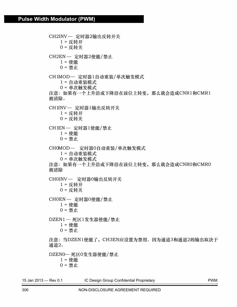
Pulse Width Modulator (PWM)
CH2INV — 定时器2输出反转开关1 = 反转开0 = 反转关
CH2EN — 定时器2使能/禁止1 = 使能0 = 禁止
CH1MOD — 定时器1自动重装/单次触发模式1 = 自动重装模式0 = 单次触发模式
注意:如果有一个上升沿或下降沿在该位上转变,那么就会造成CNR1和CMR1被清除。
CH1INV — 定时器1输出反转开关1 = 反转开0 = 反转关
CH1EN — 定时器1使能/禁止1 = 使能0 = 禁止
CH0MOD — 定时器0自动重装/单次触发模式1 = 自动重装模式0 = 单次触发模式
注意:如果有一个上升沿或下降沿在该位上转变,那么就会造成CNR0和CMR0被清除
CH0INV — 定时器0输出反转开关1 = 反转开0 = 反转关
CH0EN — 定时器0使能/禁止1 = 使能0 = 禁止
DZEN1 — 死区1发生器使能/禁止1 = 使能0 = 禁止
注意:当DZEN1使能了,CH3EN应设置为禁用。因为通道3和通道2的输出取决于通道2。
DZEN0— 死区0发生器使能/禁止1 = 使能0 = 禁止
15 Jan 2013 — Rev 0.1 IC Design Group Confidential Proprietary PWM
306 NON-DISCLOSURE AGREEMENT REQUIRED

Pulse Width Modulator (PWM) Memory Map and Registers
注意:当DZEN0使能了,CH1EN应设置为禁用。因为通道1和通道0的输出取决于通道0。
PWM IC Design Group Confidential Proprietary 15 Jan 2013 — Rev 0.1
NON-DISCLOSURE AGREEMENT REQUIRED 307

Pulse Width Modulator (PWM)
20.5.2.4 PWM计数器寄存器(PCNR0/1/2/3)
该寄存器通过设置周期里的脉冲的个数来控制PWM的周期。
地址 : 0x000c 和0x000f31 30 29 28 27 26 25 24
R 0W
RESET: 0 0 0 0 0 0 0 0
23 22 21 20 19 18 17 16R 0W
RESET: 0 0 0 0 0 0 0 0
15 14 13 12 11 10 9 8R
CNR0[15:8]W
RESET: 0 0 0 0 0 0 0 0
7 6 5 4 3 2 1 0R
CNR0[7:0]W
RESET: 0 0 0 0 0 0 0 0
= Writes have no effect and the access terminates without a transfer error exception.
地址 : 0x0018 和 0x001b31 30 29 28 27 26 25 24
R 0W
RESET: 0 0 0 0 0 0 0 0
23 22 21 20 19 18 17 16R 0W
RESET: 0 0 0 0 0 0 0 0
15 14 13 12 11 10 9 8R
CNR1[15:8]W
RESET: 0 0 0 0 0 0 0 0
7 6 5 4 3 2 1 0R
CNR1[7:0]W
RESET: 0 0 0 0 0 0 0 0
= Writes have no effect and the access terminates without a transfer error exception.
15 Jan 2013 — Rev 0.1 IC Design Group Confidential Proprietary PWM
308 NON-DISCLOSURE AGREEMENT REQUIRED

Pulse Width Modulator (PWM) Memory Map and Registers
图 20-5 PWM计数器寄存器 (PCNR)
地址: 0x0024和0x002731 30 29 28 27 26 25 24
R 0W
RESET: 0 0 0 0 0 0 0 0
23 22 21 20 19 18 17 16R 0W
RESET: 0 0 0 0 0 0 0 0
15 14 13 12 11 10 9 8R
CNR2[15:8]W
RESET: 0 0 0 0 0 0 0 0
7 6 5 4 3 2 1 0R
CNR2[7:0]W
RESET: 0 0 0 0 0 0 0 0
= Writes have no effect and the access terminates without a transfer error exception.
地址: 0x0030 and 0x003331 30 29 28 27 26 25 24
R 0W
RESET: 0 0 0 0 0 0 0 0
23 22 21 20 19 18 17 16R 0W
RESET: 0 0 0 0 0 0 0 0
15 14 13 12 11 10 9 8R
CNR3[15:8]W
RESET: 0 0 0 0 0 0 0 0
7 6 5 4 3 2 1 0R
CNR3[7:0]W
RESET: 0 0 0 0 0 0 0 0
= Writes have no effect and the access terminates without a transfer error exception.
PWM IC Design Group Confidential Proprietary 15 Jan 2013 — Rev 0.1
NON-DISCLOSURE AGREEMENT REQUIRED 309

Pulse Width Modulator (PWM)
CNR[15:0] — PWM计数器/定时器载入值插入数据的范围:65535~0 (单位 : 1个PWM时钟周期)
注1:一个PWM周期宽度= CNR + 1。如果CNR等于零,PWM计数器/定时器将停止。
注2:程序员可以在任何时候往CNR写入任何数据,并且在下一个PWM计数器周期起作用
15 Jan 2013 — Rev 0.1 IC Design Group Confidential Proprietary PWM
310 NON-DISCLOSURE AGREEMENT REQUIRED

Pulse Width Modulator (PWM) Memory Map and Registers
20.5.2.5 PWM比较器寄存器(PCMR0/1/2/3)
该寄存器定义了脉冲宽度。当计数器的值与该寄存器内的值匹配时,the output is reset for the duration of the period..地址 : 0x0010和0x0013
31 30 29 28 27 26 25 24R 0W
RESET: 0 0 0 0 0 0 0 0
23 22 21 20 19 18 17 16R 0W
RESET: 0 0 0 0 0 0 0 0
15 14 13 12 11 10 9 8R
CMR0[15:8]W
RESET: 0 0 0 0 0 0 0 0
7 6 5 4 3 2 1 0R
CMR0[7:0]W
RESET: 0 0 0 0 0 0 0 0
= Writes have no effect and the access terminates without a transfer error exception.
地址: 0x001c和0x001f31 30 29 28 27 26 25 24
R 0W
RESET: 0 0 0 0 0 0 0 0
23 22 21 20 19 18 17 16R 0W
RESET: 0 0 0 0 0 0 0 0
15 14 13 12 11 10 9 8R
CMR1[15:8]W
RESET: 0 0 0 0 0 0 0 0
7 6 5 4 3 2 1 0R
CMR1[7:0]W
RESET: 0 0 0 0 0 0 0 0
= Writes have no effect and the access terminates without a transfer error exception.
PWM IC Design Group Confidential Proprietary 15 Jan 2013 — Rev 0.1
NON-DISCLOSURE AGREEMENT REQUIRED 311

Pulse Width Modulator (PWM)
图20-6 PWM比较器寄存器(PCMR)
地址: 0x0028和0x002b31 30 29 28 27 26 25 24
R 0W
RESET: 0 0 0 0 0 0 0 0
23 22 21 20 19 18 17 16R 0W
RESET: 0 0 0 0 0 0 0 0
15 14 13 12 11 10 9 8R
CMR2[15:8]W
RESET: 0 0 0 0 0 0 0 0
7 6 5 4 3 2 1 0R
CMR2[7:0]W
RESET: 0 0 0 0 0 0 0 0
= Writes have no effect and the access terminates without a transfer error exception.
地址: 0x0034和0x003731 30 29 28 27 26 25 24
R 0W
RESET: 0 0 0 0 0 0 0 0
23 22 21 20 19 18 17 16R 0W
RESET: 0 0 0 0 0 0 0 0
15 14 13 12 11 10 9 8R
CMR3[15:8]W
RESET: 0 0 0 0 0 0 0 0
7 6 5 4 3 2 1 0R
CMR3[7:0]W
RESET: 0 0 0 0 0 0 0 0
= Writes have no effect and the access terminates without a transfer error exception.
15 Jan 2013 — Rev 0.1 IC Design Group Confidential Proprietary PWM
312 NON-DISCLOSURE AGREEMENT REQUIRED

Pulse Width Modulator (PWM) Memory Map and Registers
CMR[15:0] — PWM比较寄存器插入的数据的范围:65535~0 (unit=1个PWM时钟周期)
CMR用来决定PWM的输出占空比。
Assumption : PWM output initial : high
CMR >= CNR : PWM输出一直是高
CMR < CNR : PWM输出高脉宽= (CMR +1) unit
CMR = 0 : PWM输出高脉宽= 1 unit
Note 1:PWM duty = CMR + 1. If CMR equal zero, PWM duty = 1
注2:程序员可以在任何时候往CMR写入任何数据,并且在下一个PWM计数器周期起作用。
3 234012
1
401
1
3
0
4
CMR
CNR
PWM output
CMR=1CNR=3
Auto reload=1CHxMOD=1
Set CHxEN=1
CMR=0CNR=4
Auto-load Auto-load
PWM IC Design Group Confidential Proprietary 15 Jan 2013 — Rev 0.1
NON-DISCLOSURE AGREEMENT REQUIRED 313

Pulse Width Modulator (PWM)
101 51 1
WriteCMR=100
WriteCMR=50 Write
CMR=0
PWM cycle=151 PWM cycle=151 PWM cycle=151
Modulate PWM Controller output duty ratio (CNR=150)
15 Jan 2013 — Rev 0.1 IC Design Group Confidential Proprietary PWM
314 NON-DISCLOSURE AGREEMENT REQUIRED

Pulse Width Modulator (PWM) Memory Map and Registers
20.5.2.6 PWM定时器寄存器(PTR0/1/2/3)
PWM定时器寄存器是一个只读寄存器,作用是保持当前的计数值。该寄存器中的数据可以随时被读出而不需要惊动计数器。
地址: 0x0014和 0x001731 30 29 28 27 26 25 24
R 0W
RESET: 0 0 0 0 0 0 0 0
23 22 21 20 19 18 17 16R 0W
RESET: 0 0 0 0 0 0 0 0
15 14 13 12 11 10 9 8R PTR0[15:8]W
RESET: 0 0 0 0 0 0 0 0
7 6 5 4 3 2 1 0R PTR0[7:0]W
RESET: 0 0 0 0 0 0 0 0
= Writes have no effect and the access terminates without a transfer error exception.
地址 : 0x0020和 0x002331 30 29 28 27 26 25 24
R 0W
RESET: 0 0 0 0 0 0 0 0
23 22 21 20 19 18 17 16R 0W
RESET: 0 0 0 0 0 0 0 0
15 14 13 12 11 10 9 8R PTR1[15:8]W
RESET: 0 0 0 0 0 0 0 0
7 6 5 4 3 2 1 0R PTR1[7:0]W
RESET: 0 0 0 0 0 0 0 0
= Writes have no effect and the access terminates without a transfer error exception.
PWM IC Design Group Confidential Proprietary 15 Jan 2013 — Rev 0.1
NON-DISCLOSURE AGREEMENT REQUIRED 315

Pulse Width Modulator (PWM)
Figure 20-7 PWM Timer Register (PTR)
地址: 0x002c和0x002f31 30 29 28 27 26 25 24
R 0W
RESET: 0 0 0 0 0 0 0 0
23 22 21 20 19 18 17 16R 0W
RESET: 0 0 0 0 0 0 0 0
15 14 13 12 11 10 9 8R PTR2[15:8]W
RESET: 0 0 0 0 0 0 0 0
7 6 5 4 3 2 1 0R PTR2[7:0]W
RESET: 0 0 0 0 0 0 0 0
= Writes have no effect and the access terminates without a transfer error exception.
地址: 0x0038和0x003b31 30 29 28 27 26 25 24
R 0W
RESET: 0 0 0 0 0 0 0 0
23 22 21 20 19 18 17 16R 0W
RESET: 0 0 0 0 0 0 0 0
15 14 13 12 11 10 9 8R PTR3[15:8]W
RESET: 0 0 0 0 0 0 0 0
7 6 5 4 3 2 1 0R PTR3[7:0]W
RESET: 0 0 0 0 0 0 0 0
= Writes have no effect and the access terminates without a transfer error exception.
15 Jan 2013 — Rev 0.1 IC Design Group Confidential Proprietary PWM
316 NON-DISCLOSURE AGREEMENT REQUIRED

Pulse Width Modulator (PWM) Memory Map and Registers
PTR[15:0] — PWM定时器数值该位是可读位,作用是保持当前的计数值。用户可以通过监控PTR来获取16位向下计数器的当前的数值。
PWM IC Design Group Confidential Proprietary 15 Jan 2013 — Rev 0.1
NON-DISCLOSURE AGREEMENT REQUIRED 317

Pulse Width Modulator (PWM)
20.5.2.7 PWM中断使能寄存器(PIER)
该寄存器是用来使能PWM定时器中断的。
图20-8 PWM中断使能寄存器(PIER)
PIER3 — PWM定时器3中断使能1 = 使能0 = 禁止
PIER2 — PWM定时器2中断使能1 = 使能0 = 禁止
PIER1 — PWM定时器1中断使能1 = 使能0 = 禁止
PIER0 — PWM定时器0中断使能1 = 使能0 = 禁止
地址: 0x003c和 0x003f31 30 29 28 27 26 25 24
R 0W
RESET: 0 0 0 0 0 0 0 0
23 22 21 20 19 18 17 16R 0W
RESET: 0 0 0 0 0 0 0 0
15 14 13 12 11 10 9 8R 0W
RESET: 0 0 0 0 0 0 0 0
7 6 5 4 3 2 1 0R 0
PIER3 PIER2 PIER1 PIER0W
RESET: 0 0 0 0 0 0 0 0
= Writes have no effect and the access terminates without a transfer error exception.
15 Jan 2013 — Rev 0.1 IC Design Group Confidential Proprietary PWM
318 NON-DISCLOSURE AGREEMENT REQUIRED
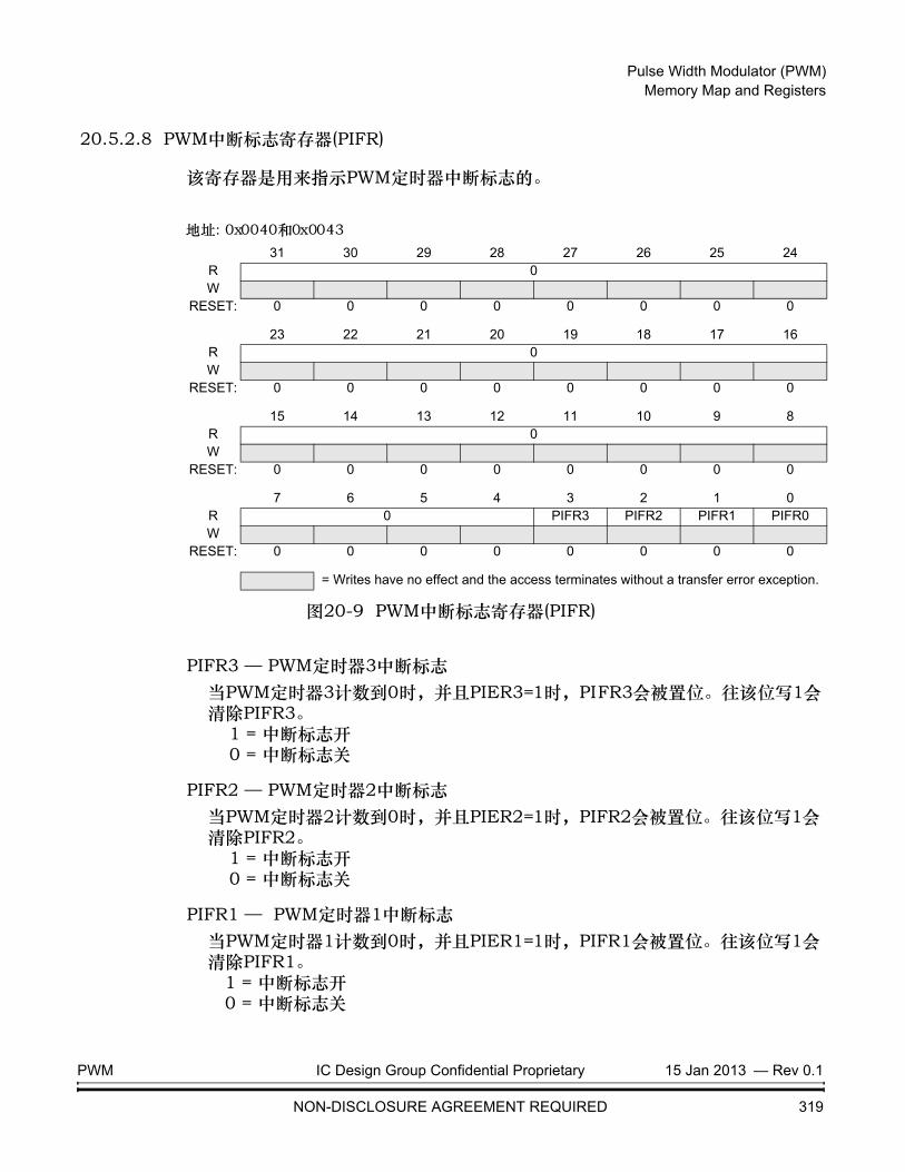
Pulse Width Modulator (PWM) Memory Map and Registers
20.5.2.8 PWM中断标志寄存器(PIFR)
该寄存器是用来指示PWM定时器中断标志的。
图20-9 PWM中断标志寄存器(PIFR)
PIFR3 — PWM定时器3中断标志当PWM定时器3计数到0时,并且PIER3=1时,PIFR3会被置位。往该位写1会清除PIFR3。
1 = 中断标志开0 = 中断标志关
PIFR2 — PWM定时器2中断标志当PWM定时器2计数到0时,并且PIER2=1时,PIFR2会被置位。往该位写1会清除PIFR2。
1 = 中断标志开0 = 中断标志关
PIFR1 — PWM定时器1中断标志当PWM定时器1计数到0时,并且PIER1=1时,PIFR1会被置位。往该位写1会清除PIFR1。 1 = 中断标志开 0 = 中断标志关
地址: 0x0040和0x004331 30 29 28 27 26 25 24
R 0W
RESET: 0 0 0 0 0 0 0 0
23 22 21 20 19 18 17 16R 0W
RESET: 0 0 0 0 0 0 0 0
15 14 13 12 11 10 9 8R 0W
RESET: 0 0 0 0 0 0 0 0
7 6 5 4 3 2 1 0R 0 PIFR3 PIFR2 PIFR1 PIFR0W
RESET: 0 0 0 0 0 0 0 0
= Writes have no effect and the access terminates without a transfer error exception.
PWM IC Design Group Confidential Proprietary 15 Jan 2013 — Rev 0.1
NON-DISCLOSURE AGREEMENT REQUIRED 319

Pulse Width Modulator (PWM)
PIFR0 — PWM定时器0中断标志当PWM定时器0计数到0时,并且PIER0=1时,PIFR0会被置位。往该位写1会清除PIFR0。
1 = 中断标志开0 = 中断标志关
15 Jan 2013 — Rev 0.1 IC Design Group Confidential Proprietary PWM
320 NON-DISCLOSURE AGREEMENT REQUIRED

Pulse Width Modulator (PWM) Memory Map and Registers
20.5.2.9 PWM捕获控制寄存器 (PCCR0/1)
该寄存器是用来控制捕获功能的。
图20-10 PWM捕获控制寄存器(PCCR0/1)
地址: 0x0044和 0x004731 30 29 28 27 26 25 24
R 0W
RESET: 0 0 0 0 0 0 0 0
23 22 21 20 19 18 17 16R CFLRD1 CRLRD1 0 CAPIF1 CAPCH1
ENFL_IE1 RL_IE1 INV1
WRESET: 0 0 0 0 0 0 0 0
15 14 13 12 11 10 9 8R 0W
RESET: 0 0 0 0 0 0 0 0
7 6 5 4 3 2 1 0R CFLRD0 CRLRD0 0 CAPIF0 CAPCH0
ENFL_IE0 RL_IE0 INV0
WRESET: 0 0 0 0 0 0 0 0
= Writes have no effect and the access terminates without a transfer error exception.
地址: 0x0048和 0x004b31 30 29 28 27 26 25 24
R 0W
RESET: 0 0 0 0 0 0 0 0
23 22 21 20 19 18 17 16R CFLRD3 CRLRD3 0 CAPIF3 CAPCH3
ENFL_IE3 RL_IE3 INV3
WRESET: 0 0 0 0 0 0 0 0
15 14 13 12 11 10 9 8R 0W
RESET: 0 0 0 0 0 0 0 0
7 6 5 4 3 2 1 0R CFLRD2 CRLRD2 0 CAPIF2 CAPCH2
ENFL_IE2 RL_IE2 INV2
WRESET: 0 0 0 0 0 0 0 0
= Writes have no effect and the access terminates without a transfer error exception.
PWM IC Design Group Confidential Proprietary 15 Jan 2013 — Rev 0.1
NON-DISCLOSURE AGREEMENT REQUIRED 321

Pulse Width Modulator (PWM)
CFLRDx — 捕获下降锁存寄存器装载标志1 = 当输入通道x有一个下降跳变时,CFLRx会被更新,并且该位被置1。
0 = 当输入通道x没有下降跳变时。 写1可清除该位。
CRLRDx— 捕获上升锁存寄存器装载标志1 = 当输入通道x有一个上升跳变时,CRLRx会被更新,并且该位被置1。0 = 输入通道x没有上升跳变时。
写1可清除该位。
CAPIFx— 捕获通道x中断标志1 = 当输入通道x有一个下降跳变,并且FL&IEx位使能时,该中断标志会被 置位。当输入通道x有一个上升跳变,并且RL&IEx位使能时,该中断标
志同样被置位。 0 = 捕获通道x中断标志没有被置位。 写1可清除该位。
CAPCHxEN— 捕获通道x使能/禁止1 = 使能0 = 禁止
当该位使能时,捕获会锁存PMW计数器,并且保存CRLR (上升锁存)和CFLR (下降锁存)。当该位禁止时,捕获不会更新CRLR和CFLR,并且禁止通道x的中断。
FL_IEx — 通道x下降中断使能开关1 = 使能0 = 禁止
当该位使能时,如果不会检测到通道x有一个下降跳变,那么捕获会产生一个中断。 RL_IEx — 通道x上升中断使能开关
1 = 使能0 = 禁止
当该位使能时,如果不会检测到通道x有一个上升跳变,那么捕获会产生一个中断。
INVx — 通道x反转开关1 = 反转开
15 Jan 2013 — Rev 0.1 IC Design Group Confidential Proprietary PWM
322 NON-DISCLOSURE AGREEMENT REQUIRED

Pulse Width Modulator (PWM) Memory Map and Registers
0 = 反转关
PWM IC Design Group Confidential Proprietary 15 Jan 2013 — Rev 0.1
NON-DISCLOSURE AGREEMENT REQUIRED 323

Pulse Width Modulator (PWM)
20.5.2.10 PWM捕获上升锁存寄存器(PCRLR0/1/2/3)
当捕获到上升跳变时,该位是用来锁存PWM计数器的。
地址 : 0x004c和0x004f31 30 29 28 27 26 25 24
R 0W
RESET: 0 0 0 0 0 0 0 0
23 22 21 20 19 18 17 16R 0W
RESET: 0 0 0 0 0 0 0 0
15 14 13 12 11 10 9 8R CRLR0[15:8]W
RESET: 0 0 0 0 0 0 0 0
7 6 5 4 3 2 1 0R CRLR0[7:0]W
RESET: 0 0 0 0 0 0 0 0
= Writes have no effect and the access terminates without a transfer error exception.
地址 : 0x0054和 0x005731 30 29 28 27 26 25 24
R 0W
RESET: 0 0 0 0 0 0 0 0
23 22 21 20 19 18 17 16R 0W
RESET: 0 0 0 0 0 0 0 0
15 14 13 12 11 10 9 8R CRLR1[15:8]W
RESET: 0 0 0 0 0 0 0 0
7 6 5 4 3 2 1 0R CRLR1[7:0]W
RESET: 0 0 0 0 0 0 0 0
= Writes have no effect and the access terminates without a transfer error exception.
15 Jan 2013 — Rev 0.1 IC Design Group Confidential Proprietary PWM
324 NON-DISCLOSURE AGREEMENT REQUIRED

Pulse Width Modulator (PWM) Memory Map and Registers
图 20-11 PWM捕获上升锁存寄存器(PCRLR0/1/2/3)
CRLRx[15:0] — 捕获上升锁存寄存器x
当捕获到上升跳变时,该位是用来锁存PWM计数器的。
地址: 0x005c和0x005f31 30 29 28 27 26 25 24
R 0W
RESET: 0 0 0 0 0 0 0 0
23 22 21 20 19 18 17 16R 0W
RESET: 0 0 0 0 0 0 0 0
15 14 13 12 11 10 9 8R CRLR2[15:8]W
RESET: 0 0 0 0 0 0 0 0
7 6 5 4 3 2 1 0R CRLR2[7:0]W
RESET: 0 0 0 0 0 0 0 0
= Writes have no effect and the access terminates without a transfer error exception.
地址: 0x0064和 0x006731 30 29 28 27 26 25 24
R 0W
RESET: 0 0 0 0 0 0 0 0
23 22 21 20 19 18 17 16R 0W
RESET: 0 0 0 0 0 0 0 0
15 14 13 12 11 10 9 8R CRLR3[15:8]W
RESET: 0 0 0 0 0 0 0 0
7 6 5 4 3 2 1 0R CRLR3[7:0]W
RESET: 0 0 0 0 0 0 0 0
= Writes have no effect and the access terminates without a transfer error exception.
PWM IC Design Group Confidential Proprietary 15 Jan 2013 — Rev 0.1
NON-DISCLOSURE AGREEMENT REQUIRED 325

Pulse Width Modulator (PWM)
20.5.2.11 PWM捕获下降锁存寄存器(PCFLR0/1/2/3)
当捕获到下降跳变时,该位是用来锁存PWM计数器的。
地址: 0x0050和0x005331 30 29 28 27 26 25 24
R 0W
RESET: 0 0 0 0 0 0 0 0
23 22 21 20 19 18 17 16R 0W
RESET: 0 0 0 0 0 0 0 0
15 14 13 12 11 10 9 8R CFLR0[15:8]W
RESET: 0 0 0 0 0 0 0 0
7 6 5 4 3 2 1 0R CFLR0[7:0]W
RESET: 0 0 0 0 0 0 0 0
= Writes have no effect and the access terminates without a transfer error exception.
地址: 0x0058和 0x005b31 30 29 28 27 26 25 24
R 0W
RESET: 0 0 0 0 0 0 0 0
23 22 21 20 19 18 17 16R 0W
RESET: 0 0 0 0 0 0 0 0
15 14 13 12 11 10 9 8R CFLR1[15:8]W
RESET: 0 0 0 0 0 0 0 0
7 6 5 4 3 2 1 0R CFLR1[7:0]W
RESET: 0 0 0 0 0 0 0 0
= Writes have no effect and the access terminates without a transfer error exception.
15 Jan 2013 — Rev 0.1 IC Design Group Confidential Proprietary PWM
326 NON-DISCLOSURE AGREEMENT REQUIRED

Pulse Width Modulator (PWM) Memory Map and Registers
图20-12 PWM捕获下降锁存寄存器(PCFLR0/1/2/3)
CFLRx[15:0] — 捕获下降锁存寄存器x
当捕获到下降跳变时,该位是用来锁存PWM计数器的。
地址: 0x0060和 0x006331 30 29 28 27 26 25 24
R 0W
RESET: 0 0 0 0 0 0 0 0
23 22 21 20 19 18 17 16R 0W
RESET: 0 0 0 0 0 0 0 0
15 14 13 12 11 10 9 8R CFLR2[15:8]W
RESET: 0 0 0 0 0 0 0 0
7 6 5 4 3 2 1 0R CFLR2[7:0]W
RESET: 0 0 0 0 0 0 0 0
= Writes have no effect and the access terminates without a transfer error exception.
地址: 0x0068和0x006b31 30 29 28 27 26 25 24
R 0W
RESET: 0 0 0 0 0 0 0 0
23 22 21 20 19 18 17 16R 0W
RESET: 0 0 0 0 0 0 0 0
15 14 13 12 11 10 9 8R CFLR3[15:8]W
RESET: 0 0 0 0 0 0 0 0
7 6 5 4 3 2 1 0R CFLR3[7:0]W
RESET: 0 0 0 0 0 0 0 0
= Writes have no effect and the access terminates without a transfer error exception.
PWM IC Design Group Confidential Proprietary 15 Jan 2013 — Rev 0.1
NON-DISCLOSURE AGREEMENT REQUIRED 327

Pulse Width Modulator (PWM)
20.5.2.12 PWM端口控制寄存器 (PPCR)
该寄存器(PPCR)是用来控制PWMx的引脚方向和引脚状态的。
图20-13 PWM端口控制寄存器(PPCR)
PDDR[3:0] — 端口数据方向寄存器 PDDR[3:0]位控制着PWM引脚的方向。复位清除PDDR[3:0]。
1 = 相应引脚配置为输出0 = 相应引脚配置为输入
PULLUP_EN[3:0] —端口上拉使能
PULLUP_EN[3:0]位控制着PWM的上拉。
1 = 使能上拉0 = 禁止上拉
PDR[3:0] — 端口数据寄存器只有当引脚配置为通用输出时,数据写入PDR[3:0]才能驱动引脚。读输入引脚(PDDR为0)会返回引脚的电平。
地址: 0x006c和0x006f31 30 29 28 27 26 25 24
R 0W
RESET: 0 0 0 0 0 0 0 0
23 22 21 20 19 18 17 16R 0
PDDR[3:0]W
RESET: 0 0 0 0 0 0 0 0
15 14 13 12 11 10 9 8R 0
PULLUP_EN[3:0]W
RESET: 0 0 0 0 1 1 1 1
7 6 5 4 3 2 1 0R 0
PDR[3:0]W
RESET: 0 0 0 0 0 0 0 0
= Writes have no effect and the access terminates without a transfer error exception.
15 Jan 2013 — Rev 0.1 IC Design Group Confidential Proprietary PWM
328 NON-DISCLOSURE AGREEMENT REQUIRED

Pulse Width Modulator (PWM) Functional Descriptions
20.6 功能描述
本小节描述了PWM的功能操作。
20.6.1 PWM双缓冲和自动重装
PWM定时器具有双缓冲的功能,允许重装值在下一定时器操作时生效而不需要停止当前的定时器操作。虽然新的定时器值已经设置了,但是当前定时器的操作仍会继续,直到操作完成。计数器的值可以写进CNR0~3中,并且当前计数器的值可以从PTR0~3中读出。当向下计数器计数到0时,自动重载操作将从CNR0 ~ 3复制到向下计数器中。如果CNR0~3中的值为0,当计数器计数到0时,计数器会停止。如果自动重装位被设为0,计数器会立刻停止。
图20-14 PWM双缓冲图解
20.6.2 调节占空比
双缓冲操作允许CMR在当前周期的任意时刻被写入数据。装载的值将从下一周期开始生效。
Reg_CNR=150Reg_CMR=50
Start
Reg_CNR=199Reg_CMR=49
Reg_CNR=99Reg_CMR=0
Reg_CNR=0Reg_CMR=xx
Stop
15051
151 200 100
PWM_out
Write a nonzero number to prescaler & setup clock divider
PWM IC Design Group Confidential Proprietary 15 Jan 2013 — Rev 0.1
NON-DISCLOSURE AGREEMENT REQUIRED 329

Pulse Width Modulator (PWM)
图20-15 PWM控制器输出占空比
20.6.3 死区发生器
PWM is implemented with Dead Zone generator. They are built for power device protection. This function enables generation of a programmable time gap at the rising of PWM output waveform. User can program PPR [31:24] and PPR [23:16] to determine the two Dead Zone interval respectively.
图 20-16 死区发生器操作
101 51 1
WriteCMR=100
WriteCMR=50 Write
CMR=0
PWM cycle=151 PWM cycle=151 PWM cycle=151
PWM_out1
PWM_out1_n
PWM_out1_DZ
PWM_out1_n_DZ
Dead zone interval
15 Jan 2013 — Rev 0.1 IC Design Group Confidential Proprietary PWM
330 NON-DISCLOSURE AGREEMENT REQUIRED

Pulse Width Modulator (PWM) Functional Descriptions
20.6.4 PWM定时器启动流程
1. 设置时钟选择器(CSR)
2. 设置预分频和死区时间间隔 (PPR)
3. 设置反转开关,死区发生器开关,触发模式,one-shot模式,和 PWM定时器 开关 (PCR)
4. 设置比较器定时器(CMR)
5. 设置计数器寄存器(CNR)
6. 设置中断使能寄存器(PIER)
7. 设置PWMx为输出引脚(PPCR)
8. 使能PWM定时器(PCR)
20.6.5 PWM定时器停止流程
方法1:
设置16位向下计数器(CNR)为0,并且监控PTR。当PTR为0时,禁止PWM定时器 (PCR)。 (推荐)
方法2:
设置16位向下计数器(CNR)为0,当有中断请求发生时,禁止PWM定时器(PCR)。 (推荐)
方法3:
直接禁止PWM定时器(PCR)。 (不推荐)
20.6.6 捕获启动流程
1. 设置时钟选择器(CSR)
2. 设置预分频(PPR)
3. 设置反转开关, 死区发生器开关,自动重装模式/单次触发模式,和PWM定时器 开关(PCR)
4. 设置计数器寄存器(CNR)
5. 设置捕获寄存器(CCR)
PWM IC Design Group Confidential Proprietary 15 Jan 2013 — Rev 0.1
NON-DISCLOSURE AGREEMENT REQUIRED 331

Pulse Width Modulator (PWM)
6. 设置PWMx位输出引脚(PPCR)
7. 使能PWM定时器(PCR)
20.6.7 捕获基本计数器操作
图 20-17 捕获基本计数器操作
在这种情况下,CNR是8:
1. 当CAPIFx设为1时,PWM计数器CNRx会被装载。
2. 通道的低脉冲宽度为(CNR +1 – CRLR)。
7
3 2 1 8 7 6 5 8 7 6 5 4
1
5
PWM count
Capture input
CAPCHxEN
CFLR
CRLR
CFL_IE
CRL_IE
CAPIF
CFLRI
CRLR
ReloadReload
15 Jan 2013 — Rev 0.1 IC Design Group Confidential Proprietary PWM
332 NON-DISCLOSURE AGREEMENT REQUIRED

Pulse Width Modulator (PWM) Functional Descriptions
3. 通道的高脉冲宽度为(CNR +1 - CFLR)。
PWM IC Design Group Confidential Proprietary 15 Jan 2013 — Rev 0.1
NON-DISCLOSURE AGREEMENT REQUIRED 333

Pulse Width Modulator (PWM)
15 Jan 2013 — Rev 0.1 IC Design Group Confidential Proprietary PWM
334 NON-DISCLOSURE AGREEMENT REQUIRED

Advance Information — QADC
第二十一节:模数转换器(ADC)
21.1 介绍
The 12-bit ADC is a successive approximation analog-to-digital converter. It has up to 9 channels allowing it to measure signals from 8 external and 2 internal sources. A/D conversion of the various channels can be performed in single, continuous, scan or discontinuous mode. The results of the ADC are stored in a 12bit x 8depth FIFO, and the data format can be left-aligned or right-aligned.
The analog watchdog feature allows the application to detect if the input voltage goes outside the user-defined higher or lower thresholds.
An efficient low power mode is implemented to allow very low consumption at low frequency.
21.2 ADC主要特性
• 高性能
– 12位,10位,8位,6位可配置的分辨率
– ADC转换时间:12位分辨率(1MHz)的转换时间为1us,10位分辨率的 转换时间为0.88us。降低分辨率可以得到更快的转换速度。
– 可编程的采样时间
– 带内嵌数据一致性的数据对齐
– 支持DMA
• 低功耗
– 应用程序可以为低功耗操作降低PLCK频率,但仍然保持卓越的ADC性能。举个例子,不管PLCK的频率是多少,ADC仍保持1us的转换时间。
– 等待模式:防止ADC在频率较低的PLCK应用中溢出。
– Auto off mode: ADC is automatically powered off except during the active conversion phase. This dramatically reduces the power consumption of the ADC.
• 模拟输入通道
– 8个外部模拟输入口
QADC IC Design Group Confidential Proprietary Rev 0.4 — 27 Mar 2012
NON-DISCLOSURE AGREEMENT REQUIRED 335
Analog-to-digital converter (ADC) ADC main features
– 1个内部参考电压通道
– 1个内部温度传感器通道
• Start-of-conversion can be initiated:
– By software
– By hardware triggers with configurable polarity
• Conversion modes
– Can convert a single channel or can scan a sequence of channels.
– Single mode converts selected inputs once per trigger
– Continuous mode converts selected inputs continuously
– Discontinuous mode
• Interrupt generation at the end of sampling, end of conversion, end of sequence conversion, and in case of analog watchdog or overrun events.
• 模拟看门狗
• Single-ended and differential-input configurations
• Converter uses an internal reference or an external reference
QADC IC Design Group Confidential Proprietary 27 Mar 2012 — Rev 0.4
NON-DISCLOSURE AGREEMENT REQUIRED 336
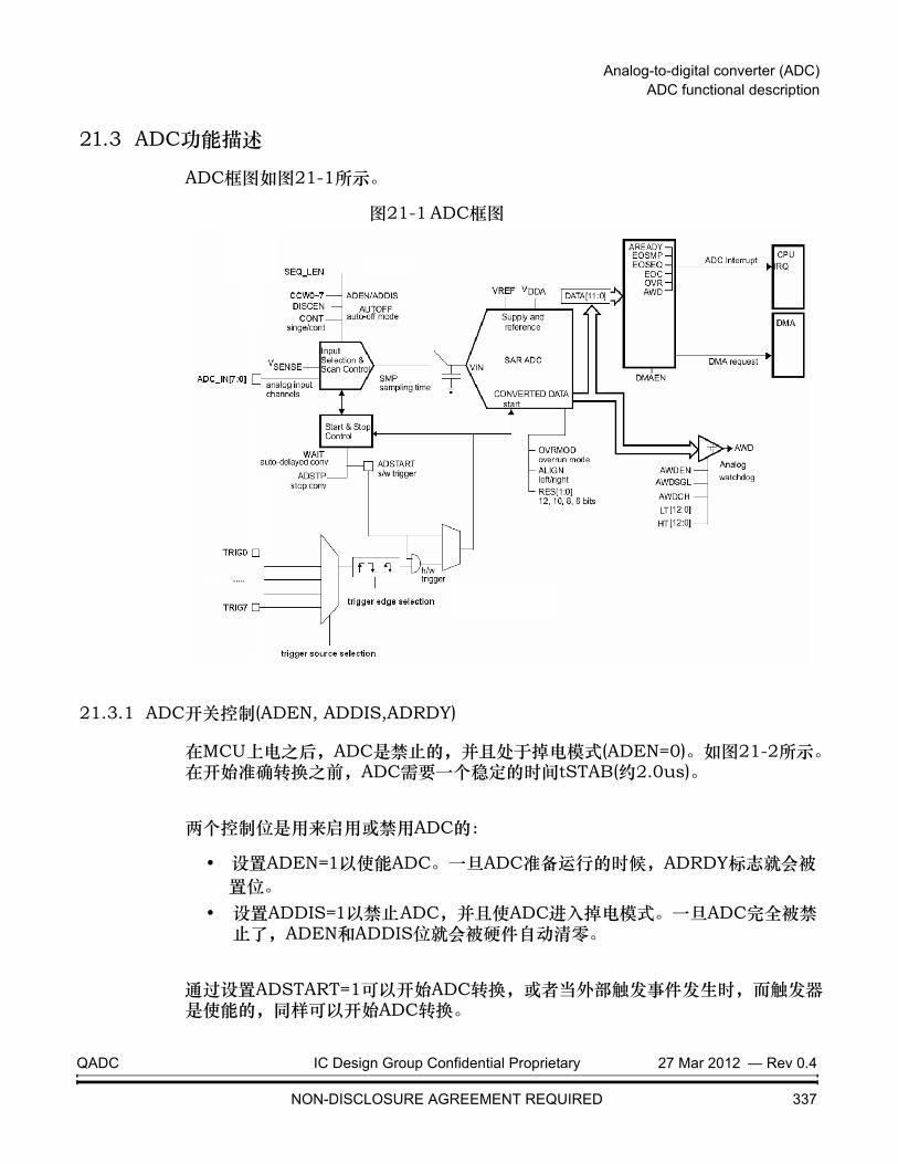
Analog-to-digital converter (ADC) ADC functional description
21.3 ADC功能描述
ADC框图如图21-1所示。
图21-1 ADC框图
21.3.1 ADC开关控制(ADEN, ADDIS,ADRDY)
在MCU上电之后,ADC是禁止的,并且处于掉电模式(ADEN=0)。如图21-2所示。 在开始准确转换之前,ADC需要一个稳定的时间tSTAB(约2.0us)。
两个控制位是用来启用或禁用ADC的:
• 设置ADEN=1以使能ADC。一旦ADC准备运行的时候,ADRDY标志就会被 置位。• 设置ADDIS=1以禁止ADC,并且使ADC进入掉电模式。一旦ADC完全被禁
止了,ADEN和ADDIS位就会被硬件自动清零。
通过设置ADSTART=1可以开始ADC转换,或者当外部触发事件发生时,而触发器是使能的,同样可以开始ADC转换。
QADC IC Design Group Confidential Proprietary 27 Mar 2012 — Rev 0.4
NON-DISCLOSURE AGREEMENT REQUIRED 337
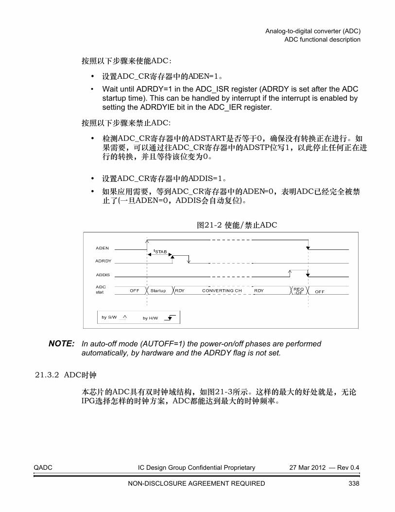
Analog-to-digital converter (ADC) ADC functional description
按照以下步骤来使能ADC:
• 设置ADC_CR寄存器中的ADEN=1。
• Wait until ADRDY=1 in the ADC_ISR register (ADRDY is set after the ADC startup time). This can be handled by interrupt if the interrupt is enabled by setting the ADRDYIE bit in the ADC_IER register.
按照以下步骤来禁止ADC:
• 检测ADC_CR寄存器中的ADSTART是否等于0,确保没有转换正在进行。如果需要,可以通过往ADC_CR寄存器中的ADSTP位写1,以此停止任何正在进行的转换,并且等待该位变为0。
• 设置ADC_CR寄存器中的ADDIS=1。
• 如果应用需要,等到ADC_CR寄存器中的ADEN=0,表明ADC已经完全被禁止了(一旦ADEN=0,ADDIS会自动复位)。
图21-2 使能/禁止ADC
NOTE: In auto-off mode (AUTOFF=1) the power-on/off phases are performed automatically, by hardware and the ADRDY flag is not set.
21.3.2 ADC时钟
本芯片的ADC具有双时钟域结构,如图21-3所示。这样的最大的好处就是,无论IPG选择怎样的时钟方案,ADC都能达到最大的时钟频率。
QADC IC Design Group Confidential Proprietary 27 Mar 2012 — Rev 0.4
NON-DISCLOSURE AGREEMENT REQUIRED 338
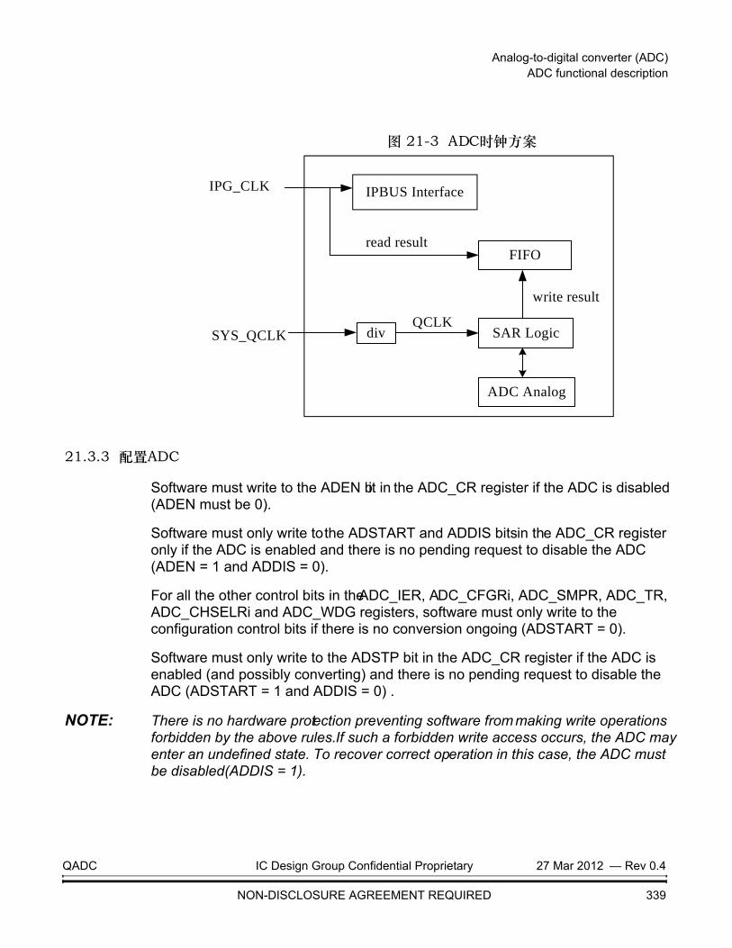
Analog-to-digital converter (ADC) ADC functional description
图 21-3 ADC时钟方案
21.3.3 配置ADC
Software must write to the ADEN bit in the ADC_CR register if the ADC is disabled (ADEN must be 0).
Software must only write to the ADSTART and ADDIS bits in the ADC_CR register only if the ADC is enabled and there is no pending request to disable the ADC (ADEN = 1 and ADDIS = 0).
For all the other control bits in the ADC_IER, ADC_CFGRi, ADC_SMPR, ADC_TR, ADC_CHSELRi and ADC_WDG registers, software must only write to the configuration control bits if there is no conversion ongoing (ADSTART = 0).
Software must only write to the ADSTP bit in the ADC_CR register if the ADC is enabled (and possibly converting) and there is no pending request to disable the ADC (ADSTART = 1 and ADDIS = 0) .
NOTE: There is no hardware protection preventing software from making write operations forbidden by the above rules. If such a forbidden write access occurs, the ADC may enter an undefined state. To recover correct operation in this case, the ADC must be disabled(ADDIS = 1).
IPBUS InterfaceIPG_CLK
SYS_QCLK div
ADC Analog
FIFO
write result
SAR Logic
read result
QCLK
QADC IC Design Group Confidential Proprietary 27 Mar 2012 — Rev 0.4
NON-DISCLOSURE AGREEMENT REQUIRED 339

Analog-to-digital converter (ADC) ADC functional description
21.3.4 通道选择(CCWi)
总共有10个多路复用通道:
• 8个模拟输入通道(ADC_IN0...ADC_IN7)
• 2个内部模拟输入通道 (VREFINT和温度传感器)
可以进行单通道转换,或者执行自动扫描通道序列转换。
要被转换的通道序列是以这种方式排列的:先是CCW[0],然后是CCW[1],... ,然后是CCW[7]。CCWi在寄存器ADC_CHSELRi中设置。序列的长度在寄存器 ADC_CFGR2中的SEQ_LEN[2:0]位配置。举个例子,如果序列长度是3,那么序列的排列方式就是CCW[0],然后是CCW[1],然后是CCW[2]。
通道解码如表21-1所示。
表 21-1 通道解码
21.3.5 可编程采样时间(SMP)
Before starting a conversion, the ADC needs to establish a direct connection between the voltage source to be measured and the embedded sampling capacitor of the ADC. This sampling time must be enough for the input voltage source to charge the sample and hold capacitor to the input voltage level.
Having a programmable sampling time allows to trim the conversion speed according to the input resistance of the input voltage source. The ADC samples the input voltage for a number of ADC clock cycles that can be modified using the
CCWi[3:0] 通道选择4’b0000 ADC_IN04’b0001 ADC_IN14’b0010 ADC_IN24’b0011 ADC_IN34’b0100 ADC_IN44’b0101 ADC_IN54’b0110 ADC_IN64’b0111 ADC_IN74’b1110 VREFINT4’b1111 温度传感器
QADC IC Design Group Confidential Proprietary 27 Mar 2012 — Rev 0.4
NON-DISCLOSURE AGREEMENT REQUIRED 340

Analog-to-digital converter (ADC) ADC functional description
SMP[3:0] bits in the ADC_SMPR register. This programmable sampling time is common to all channels.
The ADC indicates the end of the sampling phase by setting the EOSMP flag.
21.3.6 单次转换模式(CONT=0)
在单次转换模式下, ADC只执行一次转换。当ADC_CFGR1寄存器中的CONT=0时,该模式就启动了。转换也可以通过以下事件开始:
• 置位ADC_CR寄存器中的ADSTART位
• 出现硬件触发事件
Inside the sequence, after each conversion is complete:
• 转换的数据会存入FIFO中
• EOC (End Of Conversion)标志被置位
• 如果EOCIE位被置位了,中断会产生
序列转换完成之后:
• EOSEQ (End Of Sequence)标志被置位
• 如果EOSEQIE位被置位了,中断会产生
然后ADC会停止,直到下一个外部触发器事件发生,或者ADSTART被再次置位。
注意: 为了只进行一次单通道转换,转换序列的长度配置为1
21.3.7 连续转换模式 (CONT=1)
在连续转换模式下,当软件或者硬件触发事件发生时,ADC会进行序列的转换,当完成一次序列转换之后,ADC会自动重新开始,并且连续地进行相同序列的转换。当ADC_CFGR1寄存器中的CONT=1时,该模式就会启动。 转换也可以通过以下事件开始:
• 置位ADC_CR寄存器中的ADSTART位
• 硬件触发事件
Inside the sequence, after each conversion is complete:
QADC IC Design Group Confidential Proprietary 27 Mar 2012 — Rev 0.4
NON-DISCLOSURE AGREEMENT REQUIRED 341

Analog-to-digital converter (ADC) ADC functional description
• 转换的数据存储在FIFO中
• EOC (End Of Conversion)标志置位
• 如果EOCIE位置位了,中断会产生
序列转换完成之后:
• EOSEQ (End Of Sequence)标志被置位
• 如果EOSEQIE位被置位了,中断会产生
然后,新的序列又会重新开始,并且ADC会继续重复转换新序列。
注意: ADC不能同时工作在间断模式和连续模式下; 禁止同时设置DISCEN=1和CONT=1。
21.3.8 启动转换(ADSTART)
软件可通过设置ADSTART=1来启动ADC转换。
当ADSTART置位时:
• 如果TRIGMODE= 0x0 (软件触发),转换立刻开始
• At the next active edge of the selected hardware trigger if TRIGMODE ≠ 0x0
ADSTART位同样可以用来指示ADC操作是否正在进行。当ADSTART=0时,ADC可以被重新配置,表明ADC是空闲的。
ADSTART位可被硬件清除:
• 软件触发器的单次转换模式
– 在任一转换序列结束之后(EOSEQ=1)
• 软件触发器的间断转换模式
– 在任一转换结束之后
• 所有情况下
– 软件调用ADSTP程序执行之后
注意: • 在连续转换模式下(CONT=1), 当EOSEQ标志置位了,ADSTRT 位是不会硬件清除,因为序列会自动重新启动。
QADC IC Design Group Confidential Proprietary 27 Mar 2012 — Rev 0.4
NON-DISCLOSURE AGREEMENT REQUIRED 342

Analog-to-digital converter (ADC) ADC functional description
• 当单次触发模式里的硬件触发器被选择了,当EOSEQ置位时,ADSTART是 不会被硬件清零的。这就避免了软件不得不重新置位ADSTART位的情况,并 且确保下一触发事件不会丢失。
21.3.9 时序
The elapsed time between the start of a conversion and the end of conversion is the sum of the configured sampling time plus the successive approximation time depending on data resolution:
tADC = tSMPL + tSAR = [ 4|min + 12|12bit ] x tQCLK = 1μs |min (for fQCLK = 16 MHz)
图 21-4 模数转换时序
21.3.10 停止正在进行的转换(ADSTP)
软件可以通过设置ADC_CR寄存器中的ADSTP=1来停止任何正在进行的转换。
这会复位ADC操作,ADC空闲,为新的操作作准备。
当ADSTP位被软件置位时,任何正在进行的转换都会停止,同时转换的结果被丢弃。(FIFO不会更新当前的转换结果)。扫描序列同样停止和复位(这意味着启动ADC将重新开始一个新的序列)。
QADC IC Design Group Confidential Proprietary 27 Mar 2012 — Rev 0.4
NON-DISCLOSURE AGREEMENT REQUIRED 343

Analog-to-digital converter (ADC) Conversion on external trigger and trigger polarity (TRIGMODE, TRIGSCR)
一旦这个流程完成了,ADSTP和ADSTART位会被硬件清零,并且软件要在开始新的转换之前等到ADSTART=0。
注意: QADC_ISR中的标志位不会被STOP命令清除,并且FIFO中的数据不会丢失。
图21-5 停止正在进行的转换
21.4 外部触发和触发极性转换(TRIGMODE,TRIGSCR)
转换或者转换序列可以被软件或者一个外部事件触发。如果TRIGMODE的控制位不等于“0”,那么外部事件就可以触发一个选择极性的转换。一旦软件设置了ADSTART=1,那么触发器的选择就是有效的。
转换正在进行时,任何的硬件触发都会被忽略。
如果ADSTART=0,任何的硬件触发都会被忽略。
表 21-2 提供了TRIGMODE的值和触发器极性之间的对应联系。
表21-2 配置触发器极性TRIGMODE[2:0] 源
3’b000 Trigger detection disabled, software trigger 3’b001 Detection on rising edge 3’b010 Detection on falling edge3’b011 Detection on both rising and falling edges3’b100 Detection on high level voltage
QADC IC Design Group Confidential Proprietary 27 Mar 2012 — Rev 0.4
NON-DISCLOSURE AGREEMENT REQUIRED 344

Analog-to-digital converter (ADC) Conversion on external trigger and trigger polarity (TRIGMODE, TRIGSCR)
说明: 只有当ADC没有进行转换的时候 (ADSTART= 0),外部触发器的极性才能改变。
TRIGSCR控制位是用于选择8个可能触发转换的事件的,如表21-3所示。软件软触发事件可以通过置位ADC_CR寄存器中的ADSTART位来产生。
表21-3 外部触发器
说明: 只有当ADC没有进行转换的时候(ADSTART=0),触发器的选择才能改变。
21.4.1 间断模式(DISCEN)
置位ADC_CFGR1寄存器中的DISCEN位来开启间断模式。
在这个模式下(DISCEN=1),硬件或软件触发事件是需要启动每一个在序列中定义的转换 ,相反地,如果DISCEN=0,单一的硬件或软件触发事件会先后启动所有在序列中定义的转换。
例子:
• DISCEN=1,转换通道 = 0, 3, 7, 10
– 第一触发事件:通道0转换完成,EOC事件发生
– 第二触发事件:通道3转换完成,EOC事件发生
3’b101 Detection on low level votage3’b110 Detection on PIT 0 3’b111 Detection on PWM 0
TRIGSCR[2:0] 名称 源
3’b000 TRG03’b001 TRG13’b010 TRG23’b011 TRG33’b100 TRG43’b101 TRG53’b110 TRG63’b111 TRG7
QADC IC Design Group Confidential Proprietary 27 Mar 2012 — Rev 0.4
NON-DISCLOSURE AGREEMENT REQUIRED 345

Analog-to-digital converter (ADC) Conversion on external trigger and trigger polarity (TRIGMODE, TRIGSCR)
– 第三触发事件:通道7转换完成,EOC事件发生
– 第四触发事件:通道10转换完成,EOC和EOSEQ事件发生
– 第五触发事件:通道0转换完成,EOC事件发生
– 第六触发事件:通道3转换完成,EOC事件发生
– ...
• DISCEN=0,转换通道 = 0, 3, 7, 10
– 第一触发事件:完整的序列已经转换完成:先是通道0,然后是通道3、7 和10。每一次的转换都会产生一个EOC事件,并且最后一次转换会产生 EOSEQ事件。
– Any subsequent trigger events will restart the complete sequence.
21.4.2 可编程的分辨率 (RES) - 快速转换模式
通过降低ADC的精度可以有更快的转换时间(tSAR)。分辨率可以在ADC_CFGR1寄存器中的RES[1:0]位中设置,可设置为12位、10位、8位或者6位。低分辨率可以带来更快的转换时间,如果需要高精度的转换结果就不需要降低分辨率。
注意: 只有当ADEN位被复位了,RES[1:0]位中的值才能改变。
转换的结果一直都是13位宽的,并且任何没有使用的LSB位都是0。
低分辨率可以降低逐次逼近法所需的转换时间。
21.4.3 转换结束,采用相位结束(EOC, EOSMP标志)
ADC可以指示每一次ADC转换结束(EOC)事件。
只要新的转换结果是可用的,ADC就会置位ADC_ISR寄存器中的EOC标志位。如果ADC_IER寄存器中的EODIE位被置位了,那么中断就会产生。软件可以清除EOC标志位,同样可以通过往该位写1,或读FIFO来清除EOC标志。
ADC通过置位ADC_ISR寄存器里的EOSMP标志来指示采用相位的结束。软件可通过往该位写1来清除EOSMP标志。如果ADC_ISR寄存器里的EOSMPIE位被置位了,那么中断就会产生。
QADC IC Design Group Confidential Proprietary 27 Mar 2012 — Rev 0.4
NON-DISCLOSURE AGREEMENT REQUIRED 346

Analog-to-digital converter (ADC) Conversion on external trigger and trigger polarity (TRIGMODE, TRIGSCR)
21.4.4 转换序列结束 (EOSEQ flag)
The ADC notifies the application of each end of sequence (EOSEQ) event.
一旦最后一次序列转换的数据结果在FIFO中是可用的,ADC就会ADC_ISR寄存器中的EOSEQ标志。并且如果ADC_ISR寄存器中的EOSEQIE位被置位了,中断就会产生。软件可通过往该位写1来清除EOSEQ标志。
QADC IC Design Group Confidential Proprietary 27 Mar 2012 — Rev 0.4
NON-DISCLOSURE AGREEMENT REQUIRED 347

Analog-to-digital converter (ADC) Conversion on external trigger and trigger polarity (TRIGMODE, TRIGSCR)
21.4.5 实例的时序图(单次/连续模式 硬件/软件触发)
图21-6 序列单次转换,软件触发
图21-7 序列连续转换,软件触发
图21-8 序列单次转换,硬件触发
QADC IC Design Group Confidential Proprietary 27 Mar 2012 — Rev 0.4
NON-DISCLOSURE AGREEMENT REQUIRED 348

Analog-to-digital converter (ADC) Data management
图21-9 序列连续转换,硬件触发
21.5 数据管理
21.5.1 数据FIFO和数据对齐(ADC_FIFO, ALIGN )
在每个转换结束后(EOC事件发生时),转换后的数据结果储存在ADC_FIFO中。which is 13-bit wide x 8 depth.
读取的数据的格式取决于配置的数据对齐方式和分辨率。
ADC_CFGR1寄存器中的ALIGN位控制着转换结束后的数据储存的对齐方式。数据可以是右对齐(ALIGN=0)或者是左对齐(ALIGN=1)。具体如表21-10所示。
图21-10 数据对齐方式和分辨率
FIFO的支持字节,半字和字,但偏移地址应该总是0x4c。
ALIGN RES[1:0] 31 30 15 14 13 12 11 10 9 8 7 6 5 4 3 2 1 00x00x10x20x3
0x00x10x20x3
0
1
data[11:0]
data[11:0]data[9:0]
data[9:0]data[7:0]
data[5:0]
data[5:0]data[7:0]
…………
…
…
………
QADC IC Design Group Confidential Proprietary 27 Mar 2012 — Rev 0.4
NON-DISCLOSURE AGREEMENT REQUIRED 349

Analog-to-digital converter (ADC) Data management
对于不同的对齐方式和分辨率,用户应该注意:
• 如果以字的方式读出,那么数据格式是data[31:0],如图21-10所示。
• 如果以半字的方式读出,那么数据格式是data[15:0],如图21-10所示。
• 当数据长度大于8位,但是以字节的方式读出时,那么高字节的先被读出,低字节的后读出。
• 当数据长度不大于8位,但是以字节的方式读出时,那么数据格式为data[7:0]。 如图21-10所示。
21.5.2 ADC溢出(OVR, OVRMOD)
在FIFO满之前,当转换的数据没有及时地被CPU或DMA读取,那么溢出标志(OVR)就指示了一个数据溢出事件。
如果FULL标志仍然是“1”而同时新的转换已经完成,那么ADC_ISR寄存器中的OVR标志会被置位。如果ADC_IER寄存器中的OVRIE位被置位了,那么中断就会产生。
当溢出事件发生时,ADC会保持现有的操作并继续转换,除非软件决定通过置位ADC_ISR寄存器中的ADSTP位来停止和复位序列。
软件可通过往该位写1来清除OVR标志。
It is possible to configure if the data is preserved or overwritten when an overrun event occurs by programming the OVRMOD bit in the ADC_CFGR1 register:
• OVRMOD=0
– An overrun event preserves the data register from being overwritten: the old data is maintained and the new conversion is discarded. If OVR remains at 1, further conversions can be performed but the resulting data is discarded.
• OVRMOD=1
– The data register is overwritten with the last conversion result. If OVR remains at 1, further conversions can be performed and the FIFO always contains the data from the latest conversion.
21.5.3 不使用DMA来管理一个数据序列转换
如果转换足够慢,转换序列可以由软件处理。在这种情况下,软件可以使用EOC标志及其相关的中断来处理每个数据结果。每次转换完成后,ADC_ISR寄存器中的
QADC IC Design Group Confidential Proprietary 27 Mar 2012 — Rev 0.4
NON-DISCLOSURE AGREEMENT REQUIRED 350

Analog-to-digital converter (ADC) Low power features
EOC位会被置位,并且FIFO寄存器可被读出。
软件同样可以用FIFO EMPTY标志来处理每个数据结果。如果EMPTY不是“0”, 意味着FIFO接收到了新数据。
ADC_CFGR1寄存器中的OVRMOD位应被配置为0,以管理溢出事件为一个错误事件。
21.5.4 不使用DMA来管理转换的数据而不溢出
让ADC转换一个或多个通道,并且每次转换结束后都不读取结果,这是非常有用的。在这种情况下,OVRMOD位必须配置为1,并且OVR应该被软件忽略 。当OVRMOD=1时,溢出事件不会阻止ADC继续转换,并且FIFO总是包含最新的转换数据。
21.5.5 使用DMA来管理转换数据
Once the data number in the FIFO is not empty and bit DMAEN is set, QADC will send request to the DMA. This allows the transfer of the converted data from the FIFO to the destination location selected by the software.
Despite this, if an overrun occurs (OVR=1) because the DMA could not serve the DMA transfer request in time, the ADC stops generating DMA requests and the data corresponding to the new conversion is not transferred by the DMA. Which means that all the data transferred to the RAM can be considered as valid.
Depending on the configuration of OVRMOD bit, the data is either preserved or overwritten.
The DMA transfer requests are blocked until the software clears the OVR bit.
21.6 低功耗特性
21.6.1 等待模式转换
等待模式转换可以用来简化软件以及优化应用程序在低频率下的性能,低频率下会有ADC溢出的风险。当ADC_CFGR1寄存器中的WAIT位被置为1时,只有FIFO不为空时,新的转换才能开始。
QADC IC Design Group Confidential Proprietary 27 Mar 2012 — Rev 0.4
NON-DISCLOSURE AGREEMENT REQUIRED 351

Analog-to-digital converter (ADC) Analog window watchdog (AWDEN, AWDSGL, AWDCH,AWD_HTR/LTR, AWD)
This is a way to automatically adapt the speed of the ADC to the speed of the system that reads the data.
NOTE: Any hardware triggers which occur while a conversion is ongoing or during the wait time preceding the read access are ignored.
21.6.2 自动关机模式(AUTOFF)
ADC具有自动电源管理功能称为自动关机模式,通过设置ADC_CFGR1寄存器中的 AUTOFF=1来启动。
When AUTOFF=1, the ADC is always powered off when not converting and automatically wakes-up when a conversion is started (by software or hardware trigger). A startup-time is automatically inserted between the trigger event which starts the conversion and the sampling time of the ADC. The ADC is then automatically disabled once the sequence of conversions is complete.
Auto-off mode can cause a dramatic reduction in the power consumption of applications which need relatively few conversions or when conversion requests are timed far enough apart (for example with a low frequency hardware trigger) to justify the extra power and extra time used for switching the ADC on and off.
Auto-off mode can be combined with the wait mode conversion (WAIT=1) for applications clocked at low frequency. This combination can provide significant power savings if the ADC is automatically powered-off during the wait phase and restarted as soon as the FIFO is read by the application
21.7 模拟窗口看门狗(AWDEN, AWDSGL, AWDCH,AWD_HTR/LTR,AWD)
通过设置ADC_CFGR1寄存器中的AWDEN位来启动AWD模拟看门狗功能。它是用来监控一个选定通道或所有启动的,仍在配置电压范围内的通道,如图21-11所示。
如果模拟电压经ADC转换后低于或者高于模拟阈值,那么AWD模拟看门狗状态位会被置位。阈值是在ADC_TR寄存器中配置的。通过置位ADC_IER寄存器中的AWDIE位以产生一个中断。
软件可往该位写1来清除AWD标志。
当转换的数据低于12位分辨率(根据位RES [1:0]决定)时,阈值的LSB逆序保持
QADC IC Design Group Confidential Proprietary 27 Mar 2012 — Rev 0.4
NON-DISCLOSURE AGREEMENT REQUIRED 352

Analog-to-digital converter (ADC) Temperature sensor
清楚,因为内部比较总是在全12位数据转换后进行(左对齐)。
表21-4展示了怎样配置ADC_CFGR1寄存器中的AWDSGL和AWDEN位,以使能一个或多个通道上的模拟看门狗。
图21-11模拟看门狗保护区
表21-4 模拟看门狗通道选择
21.8 温度传感器
温度传感器连接到内部ADC1_IN15输入通道,用于将传感器的输出电压转换成数字值。
21.9 ADC中断
中断可由下列任何事件的产生:
• ADC上电,当ADC准备好了(ADRDY标志)
• 任意转换结束(EOC标志)
• 任意序列转换结束(EOSEQ标志)
• 当模拟看门狗检测发生 (AWD标志)
• 当采样相位结束事件发生时(EOSMP标志)
• when a data overrun occurs (OVR flag) Separate interrupt enable bits are available for flexibility.
QADC IC Design Group Confidential Proprietary 27 Mar 2012 — Rev 0.4
NON-DISCLOSURE AGREEMENT REQUIRED 353
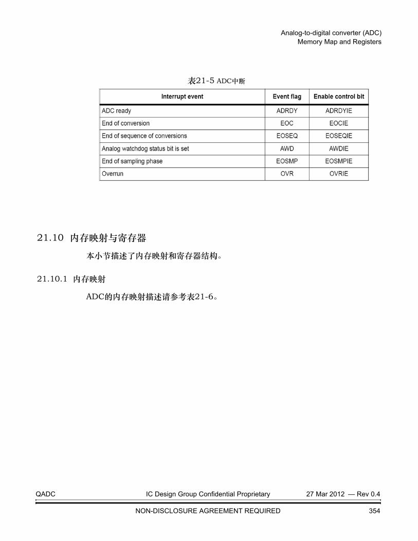
Analog-to-digital converter (ADC) Memory Map and Registers
表21-5 ADC中断
21.10 内存映射与寄存器
本小节描述了内存映射和寄存器结构。
21.10.1 内存映射
ADC的内存映射描述请参考表21-6。
QADC IC Design Group Confidential Proprietary 27 Mar 2012 — Rev 0.4
NON-DISCLOSURE AGREEMENT REQUIRED 354

Analog-to-digital converter (ADC) Memory Map and Registers
表21-6 ADC内存映射
NOTE: 1. All the registers are CPU supervisor or user mode accessable.
2. The darked bits are reserved, and must be kept at reset value.
21.10.2 寄存器
Offset Register 31
30
29
28
27
26
25
24
23
22
21
20
19
18
17
16
15
14
13
12
11
10 9 8 7 6 5 4 3 2 1 0
0x00 ADC_ISR AWD
Empty
FULL
OVR
EOSEQ
EOC
EOSMP
ADRDY
0x04 ADC_IER
AWDIE
OVRIE
EOSEQIE
EOCIE
EOSMPIE
ADRDYIE
0x08 ADC_CR
ADSTP
ADSTART
ADDIS
ADEN
0x0c ADC_CFGR1
DIFF
OVRMOD
DISCEN
AUTOFF
WAIT
CONT
ALIGN
DMAEN
0x10 ADC_CFGR2
0x14 ADC_SMPR
0x18 ADC_WDG
AWDEN
AWDSGL
0x1c ADC_TR
0x2c ADC_CHSELR1
0x30 ADC_CHSELR2
0x4c ADC_FIFO
HT[11:0]
LT[11:0]
SMP
[7:0]
STCNT
[7:0]
DATA
[15:0]
CCW4
[3:0]
AWDCH
[3:0]
CCW0
[3:0]
CCW1
[3:0]
CCW5
[3:0]
TRIGSCR
[2:0]
SEQ_LEN
[2:0]
QPR
[3:0]
RES
[1:0]
TRIGMODE
[2:0]
CCW3
[3:0]
CCW2
[3:0]
CCW7
[3:0]
CCW6
[3:0]
QADC IC Design Group Confidential Proprietary 27 Mar 2012 — Rev 0.4
NON-DISCLOSURE AGREEMENT REQUIRED 355
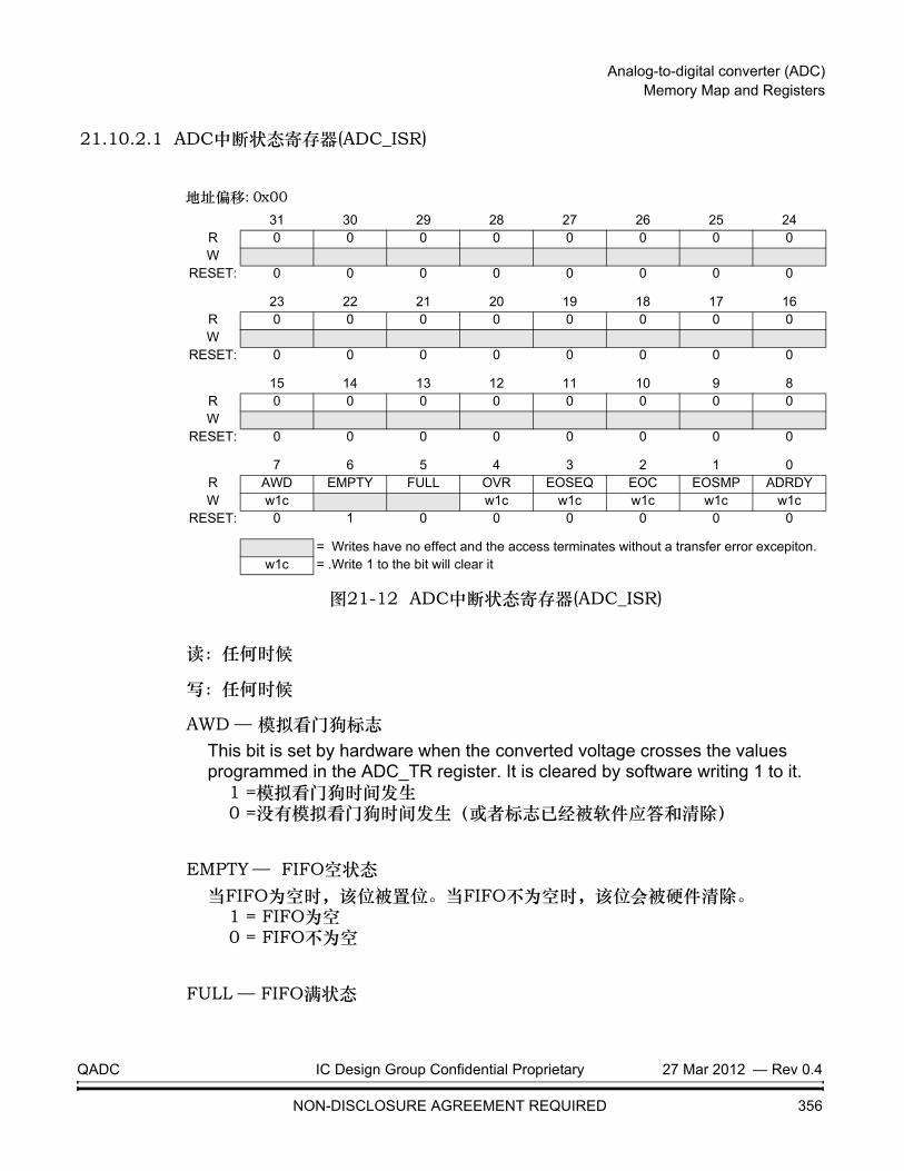
Analog-to-digital converter (ADC) Memory Map and Registers
21.10.2.1 ADC中断状态寄存器(ADC_ISR)
图21-12 ADC中断状态寄存器(ADC_ISR)
读:任何时候
写:任何时候
AWD — 模拟看门狗标志This bit is set by hardware when the converted voltage crosses the values programmed in the ADC_TR register. It is cleared by software writing 1 to it.
1 =模拟看门狗时间发生 0 =没有模拟看门狗时间发生(或者标志已经被软件应答和清除)
EMPTY — FIFO空状态当FIFO为空时,该位被置位。当FIFO不为空时,该位会被硬件清除。
1 = FIFO为空0 = FIFO不为空
FULL — FIFO满状态
地址偏移: 0x0031 30 29 28 27 26 25 24
R 0 0 0 0 0 0 0 0W
RESET: 0 0 0 0 0 0 0 0
23 22 21 20 19 18 17 16R 0 0 0 0 0 0 0 0W
RESET: 0 0 0 0 0 0 0 0
15 14 13 12 11 10 9 8R 0 0 0 0 0 0 0 0W
RESET: 0 0 0 0 0 0 0 0
7 6 5 4 3 2 1 0R AWD EMPTY FULL OVR EOSEQ EOC EOSMP ADRDYW w1c w1c w1c w1c w1c w1c
RESET: 0 1 0 0 0 0 0 0
= Writes have no effect and the access terminates without a transfer error excepiton.w1c = .Write 1 to the bit will clear it
QADC IC Design Group Confidential Proprietary 27 Mar 2012 — Rev 0.4
NON-DISCLOSURE AGREEMENT REQUIRED 356

Analog-to-digital converter (ADC) Memory Map and Registers
当FIFO为满时,该位被硬件置位。当FIFO不为满时,该位被硬件清零。1 = FIFO为满0 = FIFO不为满
OVR — ADC溢出当溢出事件发生时,该位会被硬件置位,意味着新的转换已经完成,同时FULL已经被置位。软件可通过往该位写1来清除该位。
1 = 溢出事件已经发送 0 = 没有溢出事件发生(或者标志已经被软件应答和清除)
EOSEQ — 序列结束标志 在序列转换结束之后,该位会被硬件置位。软件可往该位写1来清除该位。
1 = 序列转换完成0 = 序列转换未完成(或者标志已经被软件应答和清除)
EOC — 转换完成标志在通道转换结束之后,并且新的转换结果在ADC_FIFO寄存器中是可用的时候,该位会被硬件置位。软件可往该位写1来清除该位,或者清除ADC_FIFO寄存器 来清除该位。
1 = 通道转换完成 0 = 通道转换未完成(或者标志已经被软件应答和清除)
EOSMP — 采样结束标志采样相位结束后,在转换过程中该位会被硬件置位。
1 = 采样相位结束0 = 采样相位未结束(或者标志已经被软件应答和清除)
ADRDY — ADC ready 当ADC已经使能(ADEN=1)以后,并且ADC已经准备好接受新的请求时,该位会被硬件置位。软件可往该位写1来清除该位。
1 = ADC已经准备好开始转换0 = ADC还未准备好转换(或者标志已经被软件应答和清除)
QADC IC Design Group Confidential Proprietary 27 Mar 2012 — Rev 0.4
NON-DISCLOSURE AGREEMENT REQUIRED 357

Analog-to-digital converter (ADC) Memory Map and Registers
21.10.2.2 ADC中断使能寄存器 (ADC_IER)
图21-13 ADC 中断使能寄存器 (ADC_IER)
读:任何时候
写: 在ADC开始之前
AWDIE — 模拟看门狗中断使能 该位可被软件清零或置位以禁止或允许模拟看门狗中断。
1 = 模拟看门狗中断使能 0 = 模拟看门狗中断禁止
OVRIE — 溢出中断使能该位可被软件清零或置位以禁止或允许溢出中断。
1 = 溢出中断使能。当OVR位被置位时,中断会产生。 0 = 溢出中断禁止
EOSEQIE — 序列转换结束中断使能 该位可被软件清零或置位以禁止或允许序列转换中断。
地址偏移 : 0x0431 30 29 28 27 26 25 24
R 0 0 0 0 0 0 0 0W
RESET: 0 0 0 0 0 0 0 0
23 22 21 20 19 18 17 16R 0 0 0 0 0 0 0 0W
RESET: 0 0 0 0 0 0 0 0
15 14 13 12 11 10 9 8R 0 0 0 0 0 0 0 0W
RESET: 0 0 0 0 0 0 0 0
7 6 5 4 3 2 1 0R
AWDIE0 0
OVRIE EOSEQIE EOCIE EOSMPIE ADRDYIEW
RESET: 0 0 0 0 0 0 0 0
= Writes have no effect and the access terminates without a transfer error excepiton.
QADC IC Design Group Confidential Proprietary 27 Mar 2012 — Rev 0.4
NON-DISCLOSURE AGREEMENT REQUIRED 358

Analog-to-digital converter (ADC) Memory Map and Registers
1 = EOSEQ中断使能。当EOSEQ位被置位时,中断会产生。 0 = EOSEQ中断禁止
EOCIE — 转换结束中断使能 该位可被软件清零或置位以禁止或允许转换结束中断。
1 = EOC中断使能。当EOC位被置位时, 中断会产生 0 = EOC中断禁止
EOSMPIE — 采样结束标志中断使能 该位可被软件清零或置位以禁止或允许采样相位结束中断。
1 = EOSMP中断使能。当EOSMP位被置位时,中断会产生 0 = EOSMP中断禁止
ADRDYIE — ADC ready interrupt enable This bit is set and cleared by software to enable/disable the ADC Ready interrupt.
1 = ADRDY中断使能。当ADRDY位被置位时,中断会产生 0 = ADRDY 中断禁止
QADC IC Design Group Confidential Proprietary 27 Mar 2012 — Rev 0.4
NON-DISCLOSURE AGREEMENT REQUIRED 359

Analog-to-digital converter (ADC) Memory Map and Registers
21.10.2.3 ADC控制寄存器(ADC_CR)
图21-14 ADC控制寄存器(ADC_CR)
读:任何时候
写:参考每位的描述
ADSTP — ADC停止转换命令软件可置位该位以停止和丢弃正在进行的转换(ADSTP命令)。当转换已经有效地被丢弃了,并且ADC准备好接受新的开始转换命令后,该位会被硬件清零。
1 = Write 1 to stop the ADC. Read 1 means that an ADSTP command is in progress.
0 = No ADC stop conversion command ongoing
NOTE: Software is allowed to set ADSTP only when ADSTART=1 and ADDIS=0 (ADC is enabled and may be converting and there is no pending request to disable the ADC)
ADSTART — ADC开始转换命令
地址偏移: 0x0831 30 29 28 27 26 25 24
R 0 0 0 0 0 0 0 0W
RESET: 0 0 0 0 0 0 0 0
23 22 21 20 19 18 17 16R 0 0 0 0 0 0 0 0W
RESET: 0 0 0 0 0 0 0 0
15 14 13 12 11 10 9 8R 0 0 0 0 0 0 0 0W
RESET: 0 0 0 0 0 0 0 0
7 6 5 4 3 2 1 0R 0 0 0 0 ADSTP ADSTART ADDIS ADENW rs rs rs rs
RESET: 0 0 0 0 0 0 0 0
= Writes have no effect and the access terminates without a transfer error excepiton.rs = Software can read and set, write 0 has no effect
QADC IC Design Group Confidential Proprietary 27 Mar 2012 — Rev 0.4
NON-DISCLOSURE AGREEMENT REQUIRED 360

Analog-to-digital converter (ADC) Memory Map and Registers
This bit is set by software to start ADC conversion. Depending on the TRIGMODE configuration bits, a conversion either starts immediately (software trigger configuration) or once a hardware trigger event occurs (hardware trigger configuration). It is cleared by hardware:
– In single conversion mode when software trigger is selected : at the assertion of the End of Conversion Sequence (EOSEQ) flag.
– In discontinued conversion mode when software trigger is selected: at the assertion of the End of Conversion (EOC) flag.
– In all cases: after the execution of the ADSTP command, at the same time as the ADSTP bit is cleared by hardware.
1 = Write 1 to start the ADC. Read 1 means that the ADC is operating and may be converting.
0 = No ADC conversion is ongoing.
NOTE: Software is allowed to set ADSTART only when ADEN=1 and ADDIS=0 (ADC is enabled and there is no pending request to disable the ADC)
ADDIS — ADC禁止命令 软件可置位该位以禁止ADC (ADDIS命令) 并且驱使ADC进入掉电状态(关机状态)。一旦ADC已经有效地被禁止了,该位会被硬件清零(与此同时,ADEN
同样可以被硬件清零)。1 = Write 1 to disable the ADC. Read 1 means that an ADDIS command is in
progress. 0 = No ADDIS command ongoing
NOTE: Software is allowed to set ADDIS only when ADEN=1 and ADSTART=0 (which ensures that no conversion is ongoing)
ADEN — ADC使能命令 This bit is set by software to enable the ADC. The ADC will be effectively ready to operate once the ADRDY flag has been set. It is cleared by hardware when the ADC is disabled, after the execution of the ADDIS command.
1 = 使能ADC0 = 禁止ADC
NOTE: Software is allowed to set ADEN only when all bits of ADC_CR registers are 0 (ADSTP=0, ADSTART=0, ADDIS=0 and ADEN=0)
QADC IC Design Group Confidential Proprietary 27 Mar 2012 — Rev 0.4
NON-DISCLOSURE AGREEMENT REQUIRED 361
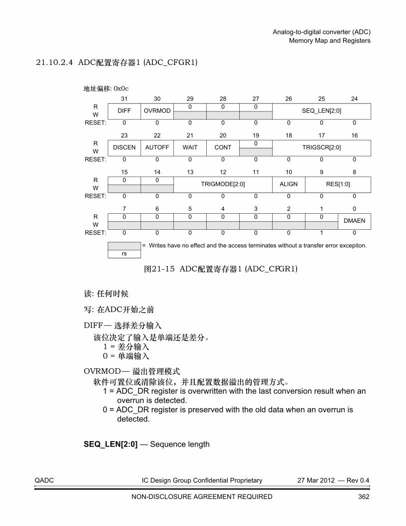
Analog-to-digital converter (ADC) Memory Map and Registers
21.10.2.4 ADC配置寄存器1 (ADC_CFGR1)
图21-15 ADC配置寄存器1 (ADC_CFGR1)
读: 任何时候
写: 在ADC开始之前
DIFF — 选择差分输入该位决定了输入是单端还是差分。
1 = 差分输入0 = 单端输入
OVRMOD — 溢出管理模式软件可置位或清除该位,并且配置数据溢出的管理方式。
1 = ADC_DR register is overwritten with the last conversion result when an overrun is detected.
0 = ADC_DR register is preserved with the old data when an overrun is detected.
SEQ_LEN[2:0] — Sequence length
地址偏移: 0x0c31 30 29 28 27 26 25 24
RDIFF OVRMOD
0 0 0SEQ_LEN[2:0]
WRESET: 0 0 0 0 0 0 0 0
23 22 21 20 19 18 17 16R
DISCEN AUTOFF WAIT CONT0
TRIGSCR[2:0]W
RESET: 0 0 0 0 0 0 0 0
15 14 13 12 11 10 9 8R 0 0
TRIGMODE[2:0] ALIGN RES[1:0]W
RESET: 0 0 0 0 0 0 0 0
7 6 5 4 3 2 1 0R 0 0 0 0 0 0 0
DMAENW
RESET: 0 0 0 0 0 0 1 0
= Writes have no effect and the access terminates without a transfer error excepiton.rs
QADC IC Design Group Confidential Proprietary 27 Mar 2012 — Rev 0.4
NON-DISCLOSURE AGREEMENT REQUIRED 362

Analog-to-digital converter (ADC) Memory Map and Registers
These bits define the length of sequence. The sequence length=SEQ_LEN+1. For example, SEQ_LEN=7 means sequence length is 8; SEQ_LEN=0 means sequence length is 1.
DISCEN — 间断模式软件可置位或清除该位以使能或禁止间断模式。
1 = 间断模式使能0 = 间断模式禁止
AUTOFF — 自动关机模式软件可置位或清除该位以使能或禁止自动关机模式。
1 = 自动关机模式使能0 = 自动关机模式禁止
WAIT — 等待转换模式软件可置位或清除该位以使能或禁止等待转换模式。
1 = 等待转换模式开0 = 等待转换模式关
CONT — 单次/连续转换模式 软件可置位和清除该位。如果置位了,那么转换就会连续不断进行,指导该位被清除。
1 = 连续转换模式0 = 单次转换模式
TRIGSCR[2:0] — 外部触发源这些位用来选择可能触发转换的8个事件。详情请参考表21-3。
TRIGMOD[2:0] — 触发模式选择这些位用于选择软件触发方式或外部触发极性,详情请参考表21-2。
ALIGN — 数据对齐方式 软件可置位和清除该位以选择右对齐还是左对齐。详情请参考图21-10。
1 = 右对齐0 = 左对齐
RES[1:0] — 数据分辨率软件可配置该位,以选择转换的分辨率。详情请参考图21-10。
DMAEN — DMA使能
QADC IC Design Group Confidential Proprietary 27 Mar 2012 — Rev 0.4
NON-DISCLOSURE AGREEMENT REQUIRED 363

Analog-to-digital converter (ADC) Memory Map and Registers
软件可置位该位以使能DMA请求。这允许使用DMA控制器控制自动转换数据。 1 = DMA使能 0 = DMA禁止
21.10.2.5 ADC配置寄存器2 (ADC_CFGR2)
图21-16 ADC配置寄存器2 (ADC_CFGR2)
读: 任何时候
写: 在ADC启动之前
QPR[3:0] — 预分频时钟位这些位选择系统时钟除数生成ADC时钟如下:
FQCLK = Fsys_QCLK / (QPR[3:0] + 1)其中:
地址偏移: 0x1031 30 29 28 27 26 25 24
R 0 0 0 0 0 0 0 0W
RESET: 0 0 0 0 0 0 0 0
23 22 21 20 19 18 17 16R 0 0 0 0 0 0 0 0W
RESET: 0 0 0 0 0 0 0 0
15 14 13 12 11 10 9 8R 0 0 0 0
QPR[3:0]W
RESET: 0 0 0 0 0 0 1 0
7 6 5 4 3 2 1 0R
STCNT[7:0]W
RESET: 0 0 1 0 0 0 0 0
= Writes have no effect and the access terminates without a transfer error excepiton.rs
QADC IC Design Group Confidential Proprietary 27 Mar 2012 — Rev 0.4
NON-DISCLOSURE AGREEMENT REQUIRED 364

Analog-to-digital converter (ADC) Memory Map and Registers
0 <= QPR[3:0] <= 15.
STCNT[7:0] — ADC启动计数器位The ADC needs a stabilization time of tSTAB(~2us) before it starts converting accurately. This time is calculated by counting QCLK cycles until the internal counter reachs the STCNT[7:0]. So user should set these bits before ADC enable. For example, if the QCLK = 16MHz, then should set the STCNT[7:0] = 2000/(1000/16)=32.
21.10.2.6 ADC采样时间寄存器(ADC_SMPR)
图21-17 ADC采样时间寄存器(ADC_SMPR)
读:任何时候
写: 在ADC启动之前
SMP[7:0] — 采样时间选择
该位由软件配置,以选择应用与所有通道的采样时间。采样时间的计算方式为: (SMP[7:0]+2) QCLKs比如 : SMP[7:0] = 0x2 意味着采样时间为4 QCLKs
地址偏移: 0x1431 30 29 28 27 26 25 24
R 0 0 0 0 0 0 0 0W
RESET: 0 0 0 0 0 0 0 0
23 22 21 20 19 18 17 16R 0 0 0 0 0 0 0 0W
RESET: 0 0 0 0 0 0 0 0
15 14 13 12 11 10 9 8R 0 0 0 0 0 0 0 0W
RESET: 0 0 0 0 0 0 1 0
7 6 5 4 3 2 1 0R
SMP[7:0]W
RESET: 0 0 0 0 0 0 1 0
= Writes have no effect and the access terminates without a transfer error excepiton.
QADC IC Design Group Confidential Proprietary 27 Mar 2012 — Rev 0.4
NON-DISCLOSURE AGREEMENT REQUIRED 365

Analog-to-digital converter (ADC) Memory Map and Registers
21.10.2.7 ADC看门狗寄存器(ADC_WDG)
图21-18 ADC看门狗寄存器(ADC_WDG)
读: 任何时候
写: 在ADC启动之前
AWDEN — 模拟看门狗使能 软件可置位和复位该位。
1 = 模拟看门狗使能 0 = 模拟看门狗禁止
AWDSGL — 在单个通道或所有通道上启动看门狗 该位由软件置位和清除。该位使能看门狗在单一通道上(由AWDCH[4:0])运行还是在所有通道上运行。
1 = 模拟看门狗在单通道上使能 0 = 模拟看门狗在所有通道上使能
AWDCH[3:0] — 模拟看门狗通道选择 这些位由软件置位和复位。该位选择由看门狗保护的输入通道。
地址偏移: 0x1831 30 29 28 27 26 25 24
R 0 0 0 0 0 0 0 0W
RESET: 0 0 0 0 0 0 0 0
23 22 21 20 19 18 17 16R 0 0 0 0 0 0 0 0W
RESET: 0 0 0 0 0 0 0 0
15 14 13 12 11 10 9 8R 0 0 0 0 0 0 0 0W
RESET: 0 0 0 0 0 0 1 0
7 6 5 4 3 2 1 0R
AWDEN AWDSGL0 0
AWDCH[3:0]W
RESET: 0 0 0 0 0 0 0 0
= Writes have no effect and the access terminates without a transfer error excepiton.
QADC IC Design Group Confidential Proprietary 27 Mar 2012 — Rev 0.4
NON-DISCLOSURE AGREEMENT REQUIRED 366

Analog-to-digital converter (ADC) Memory Map and Registers
• 0000: 由AWD监控的模拟输入通道0
• 0001: 由AWD监控的模拟输入通道1
• .....
• 0111: 由AWD监控的模拟输入通道7
• 1111: 由AWD监控的温度传感器
• 其他值:保留,禁止被使用
21.10.2.8 ADC看门狗阈值寄存器(ADC_TR)
图21-19 ADC 看门狗阈值寄存器(ADC_TR)
读: 任何时候
写: 在ADC启动之前
HT[11:0] — 模拟看门狗高阈值 这些位由软件配置,定义模拟看门狗的高阈值。
LT[11:0] — 模拟看门狗低阈值
地址偏移: 0x1c31 30 29 28 27 26 25 24
R 0 0 0 0HT[11:8]
WRESET: 0 0 0 0 0 0 0 0
23 22 21 20 19 18 17 16R
HT[7:0]W
RESET: 0 0 0 0 0 0 0 0
15 14 13 12 11 10 9 8R 0 0 0 0
LT[11:8]W
RESET: 0 0 0 0 0 0 1 0
7 6 5 4 3 2 1 0R
LT[7:0]W
RESET: 0 0 0 0 0 0 0 0
= Writes have no effect and the access terminates without a transfer error excepiton.
QADC IC Design Group Confidential Proprietary 27 Mar 2012 — Rev 0.4
NON-DISCLOSURE AGREEMENT REQUIRED 367

Analog-to-digital converter (ADC) Memory Map and Registers
这些位由软件配置,定义模拟看门狗的高阈值。
21.10.2.9 ADC通道选择寄存器(ADC_CHSELR1,ADC_CHSELR2)
图21-20 ADC通道选择寄存器1(ADC_CHSELR1)
地址偏移 : 0x2c31 30 29 28 27 26 25 24
R 0 0 0 0CCW3[3:0]
WRESET: 0 0 0 0 0 0 0 0
23 22 21 20 19 18 17 16R 0 0 0 0
CCW2[3:0]W
RESET: 0 0 0 0 0 0 0 0
15 14 13 12 11 10 9 8R 0 0 0 0
CCW1[3:0]W
RESET: 0 0 0 0 0 0 1 0
7 6 5 4 3 2 1 0R 0 0 0 0
CCW0[3:0]W
RESET: 0 0 0 0 0 0 0 0
= Writes have no effect and the access terminates without a transfer error excepiton.
QADC IC Design Group Confidential Proprietary 27 Mar 2012 — Rev 0.4
NON-DISCLOSURE AGREEMENT REQUIRED 368

Analog-to-digital converter (ADC) Memory Map and Registers
图21-21 ADC通道选择寄存器2(ADC_CHSELR2)
读: 任何时候
写: 在ADC启动之前
CCWi[3:0] — 字符 i 是选择的转换通道,详情请参考表21-1。
21.10.2.10 ADC FIFO访问寄存器(ADC_FIFO)
地址偏移 : 0x3031 30 29 28 27 26 25 24
R 0 0 0 0CCW7[3:0]
WRESET: 0 0 0 0 0 0 0 0
23 22 21 20 19 18 17 16R 0 0 0 0
CCW6[3:0]W
RESET: 0 0 0 0 0 0 0 0
15 14 13 12 11 10 9 8R 0 0 0 0
CCW5[3:0]W
RESET: 0 0 0 0 0 0 1 0
7 6 5 4 3 2 1 0R 0 0 0 0
CCW4[3:0]W
RESET: 0 0 0 0 0 0 0 0
= Writes have no effect and the access terminates without a transfer error excepiton.
QADC IC Design Group Confidential Proprietary 27 Mar 2012 — Rev 0.4
NON-DISCLOSURE AGREEMENT REQUIRED 369

Analog-to-digital converter (ADC) Memory Map and Registers
图21-22 ADC FIFO访问寄存器(ADC_FIFO)
读: 任何时候
写: 从不
DATA[15:0]: 转换的数据 参考图21-10.
地址偏移: 0x4c31 30 29 28 27 26 25 24
R 0 0 0 0 0 0 0 0W
RESET: 0 0 0 0 0 0 0 0
23 22 21 20 19 18 17 16R 0 0 0 0 0 0 0 0W
RESET: 0 0 0 0 0 0 0 0
15 14 13 12 11 10 9 8R DATA[15:8]W
RESET: 0 0 0 0 0 0 0 0
7 6 5 4 3 2 1 0R DATA[7:0]W
RESET: 0 0 0 0 0 0 0 0
= Writes have no effect and the access terminates without a transfer error excepiton.
QADC IC Design Group Confidential Proprietary 27 Mar 2012 — Rev 0.4
NON-DISCLOSURE AGREEMENT REQUIRED 370

Datasheet — LT32A01
附录A:初步的电气特性
A.1 说明
本节为LT32A01单片机提供电气参数和电气等级说明。
这些电气指标是初步的,是根据以前的设计或设计模拟得来的。在这个早期阶段的产品生命周期内,这些指标可能没有完全被测试和保证;然而生产硅芯片时将会遇到这些参数。定型的规格将会在完整的特性分析后发布,此外设备的资格已经完成。
371
LT32A01 IC Design Group Confidential Proprietary Rev 0.1 — Nov 2014
NON-DISCLOSURE AGREEMENT REQUIRED

-0.5 to +5.5
A.2 绝对最大额定参数
最大额定值是极端的限制,单片机可以在最大额定值之内正常工作而没有永久性的伤害。见表A-1。
单片机包含了保护信号输入、防止高静态电压损害的电路。不要提供比表中所示电压指标高的电压。将未使用的输入连接到适当的电压电平,或者Vssh和Vddh。此芯片是不能保证正常工作在最大额定值。参考《A.4 直流电气指标》以保证正常工作条件。
表A-1 绝对最大额定参数
序号 指标 符号 值 单位
1 电源电压 VDD -0.5 to +5.5 V
2 输入电压1 VIN V
3 瞬时最大电流限制(适用于所有管脚)
ID 12 mA
4 工作稳定范围e TOPT -40 to +85 OC
注意:
1. 输入电流必须限制在指定的值。确定所需的限流电阻的值,计算出的电阻值对于正和负钳位电压,然后使用这两个值中的较大者。
Nov 2014 — Rev 0.1 IC Design Group Confidential Proprietary LT32A01
372 NON-DISCLOSURE AGREEMENT REQUIRED

4000
A.3 静电放电(ESD)保护
表A-2 ESD保护特性参数 符号 值 单位
人体带电模型目标 HBM V
LT32A01 IC Design Group Confidential Proprietary Nov 2014 — Rev 0.1
NON-DISCLOSURE AGREEMENT REQUIRED 373

DD
5.5
5.5
A.4 直流电气指标
表A-3 直流电气指标
参数 符号 最小值 典型值 最大值 单位
电源电压 V 2.5 3.3 V
输入电压最大值 VIH 2.4 3.3 V
输入电压最小值 VIL -0.3 0 1.25 V
输出电压最大值 VOH 2.9 — — V
输出电压最小值 VOL — — 0.5 V
上拉电阻 RPU 20 100 kΩ
下拉电阻 RPU 20 100 kΩ
低电平输出电压@VOL=0.5V IOL 12 mA
高电平输出电压@VOL=2.9V IOH 12 mA
Nov 2014 — Rev 0.1 IC Design Group Confidential Proprietary LT32A01
374 NON-DISCLOSURE AGREEMENT REQUIRED

LT32A01 IC Design Group Confidential Proprietary Nov 2014 — Rev 0.1
NON-DISCLOSURE AGREEMENT REQUIRED 375

Datasheet — LT32A01
B.2 QFNWBLT32A01单片机提供以下3种封装:
附录B:机械规格B.1 介绍
7x7-48L
LT32A01 Confidential Proprietary Rev 0.1 — Nov 2014
NON-DISCLOSURE AGREEMENT REQUIRED 376

Mechanical Specifications
B.3 QFNWB5X5-32L
Nov 2014 — Rev 0.1 Confidential Proprietary LT32A01
377 NON-DISCLOSURE AGREEMENT REQUIRED China-Core

Mechanical Specifications
B.4 TSSOP24
LT32A01 Confidential Proprietary Nov 2014 — Rev 0.1
NON-DISCLOSURE AGREEMENT REQUIRED 378