Introduction to the 80386
194
-
Upload
khangminh22 -
Category
Documents
-
view
1 -
download
0
Transcript of Introduction to the 80386

inter
Introduction to the 80386 ~ncluding
the 80386 Data Sheet
April 1986

Intel Corporation makes no warranty for the use of its products and assumes no responsibility for any errors which may appear in this document nor does it make a commitment to update the information contained herein.
Intel retains the right to make changes to these specifications at any time, without notice.
Contact your local sales office to obtain the latest specifications before placing your order.
The following are trademarks of Intel Corporation and may only be used to identify Intel Products:
Above, BITBUS, COMMputer, CREDIT, Data Pipeline, FASTPATH, GENIUS, i,~, ICE, iCEL, iCS, iDBp, iDIS, 121CE, iLBX, im, iMDDX, iMMX, Insite, Intel, intel, intelBOS, Intelevision, inteligent Identifier, inteligent Programming, Intellec, Intellink, iOSP, iPDS, iPSC, iRMX, iSBC, iSBX, iSDM, iSXM, KEPROM, Library Manager, MAP-NET, MeS, Megachassis, MICROMAINFRAME, MULTIBUS, MULTICHANNEL, MULTI MODULE, ONCE, OpenNET, OTp, PC-BUBBLE, Plug-A-Bubble, PROMPT, Promware, QUEST, QueX, Quick-Pulse Programming, Ripplemode, RMX/80, RUPI, Seamless, SLD, UPI, and VLSiCEL, and the combination of ICE, iCS, iRMX, iSBC, iSBX, MCS, or UPI and a numerical suffix, 4-SITE.
MDS is an ordering code only and is not used as a product name or trademark. MDS® is a registered trademark of Mohawk Data Sciences Corporation.
'MULTI BUS is a patented Intel bus.
Additional copies of this manual or other Intel literature may be obtained from:
Intel Corporation Literature Distribution Mail Stop SC6-59 3065 Bowers Avenue Santa Clara, CA 95051
©INTEL CORPORATION 1986 3/86

TABLE OF CONTENTS BOOK I CHAPTER 1 HIGHLIGHTS
1.1 32-bit Architectu re .............................................................. 1-1 1.2 High-performance Implementation ............................................... 1-1 1.3 Virtual Memory Support ........................................................ 1~3 1.4 Configurable Protection ........................................................ 1-3 1.5 Extended Debugging Support ................................................... 1-3 1.6 Object Code Compatibility ...................................................... 1-4 1.7 Summary ..................................................................... 1-4
CHAPTER 2 APPLICATION ARCHITECTURIE
2.1 Registers ...................................................................... 2-1 2.1.1 General Registers ........................................................... 2-1 2.1.2 Flags and Instruction Pointer ................................................. 2-1 2.1.3 Numeric Coprocessor Registers .............................................. 2-2
2.2 Memory and Logical Addressing ................................................. 2-3 2.2.1 Segments .................................................................. 2-3 2.2.2 Logical Addresses .......................................................... 2-3 2.2.3 Segment and Descriptor Registers ............................................ 2-4 2.2.4 Addressing Modes .......................................................... 2-5
2.3 Data Types and Instructions ..................................................... 2-6 2.3.1 Principal Data Types ........................................................ 2-6 2.3.2 Numeric Coprocessor Data Types ............................................ 2-7 2.3.3 Other Instructions .......................................................... 2-7
2.3.3.1 Stack Instructions ....................................................... 2-7 2.3.3.2 Control Transfer Instructions ............................................. 2-8 2.3.3.3 Miscellaneous Instructions ............................................... 2-10
CHAPTER 3 SYSTEM ARCHITECTURE
3.1 System Registers ............................................................... 3-1 3.2 Multitasking ................................................................... 3-1
3.2.1 Task State Segment ......................................................... 3-2 3.2.2 Task Switching ............................................................. 3-2
3.3 Addressing .................................................................... 3-3 3.3.1 Address Translation Overview ................................................ 3-3 3.3.2 Segments ................................................................. 3-4 3.3.3 Pages ..................................................................... 3-7 3.3.4 Virtual Memory ............................................................. 3-8
iii

3.4 Protection ................................................................. 3-10 3.4.1 Privilege ................................................................ 3-10 3.4.2 Privileged Instructions .................................................... 3-12 3.4.3 Segment Protection ...................................................... 3-12 3.4.4 Page Protection ......................................................... 3-13
3.5 System Calls ............................................................... 3-13 3.6 Interrupts and Exceptions .................................................... 3-14
3.6.1 Interrupt Descriptor Table ................................................. 3-15 3.6.2 Debug Exceptions and Registers ........................................... 3-16
3.7 Input/Output ............................................................... 3-17
CHAPTER 4 ARCHITECTURAL COMPATIBILITY
4.1 80286 Compatibility ......................................................... 4-1 4.2 Real and Virtual 86 Modes .................................................... 4-1
CHAPTER 5 HARDWARE IMPLEMENTATION
5.1 Internal Design ............................................................. 5-1 5.2 External Interface ........................................................... 5-3
5.2.1 Clock .................................................................. 5-3 5.2.2 Data and Address Buses .................................................. 5-3 5.2.3 Bus Cycle Definition ..................................................... 5-4 5.2.4 Bus Cycle Control ....................................................... 5-4 5.2.5 Dynamic Bus Sizing ...................................................... 5-7 5.2.6 Processor Status and Control .............................................. 5-7 5.2.7 Coprocessor Control ..................................................... 5-7
BOOK II
80386 High Performance Microprocessor with Integrated Memory Management .............. 1
iv

Chapter 1 Highlights
1


CHAPTER 1 HIGHLIGHTS
The 80386 is a high performance 32-bit microprocessor designed to drive the most advanced computer-based applications of today and tomorrow. CAE( CAD workstations, high resolution graphics, publishing, and office and factory automation are representative of today's applications that are well-served by the 80386. Tomorrow's applications may be more constrained by the imagination of system designers than by the power and versatility of the 80386.
The 80386 offers the system designer many new and powerful capabilities, including unprecedented performance of3 to 4 million instructions per second, a complete 32-bit architecture, a 4-gigabyte (232 bytes) physical address space, and on-chip support for paged virtual memory. While embodying the latest in microprocessor technology, the 80386 retains object code compatibility with the wealth of software written for its predecessors, the 8086 and 80286. Of special interest is the 80386's virtual machine capability, which enables the 80386 to switch between programs running under different operating systems, such as Unix* and MS-DOS*. This facility enables OEMs to incorporate standard 16-bit application software directly into new 32-bit designs.
Combining the power and performance of a superminicomputer with the low cost and design versatility of a microprocessor, the 80386 can open new markets to microprocessor-based systems. Applications that have not been feasible with slower microprocessors or cost-effective with superminicomputers are now practical with the 80386. Emerging applications such as machine vision, speech recognition, advanced robots, and expert systems, which have been largely experimental, can now be brought to market.
To effectively tackle the application challenges of tomorrow requires more than 32-bit registers, instructions, and buses. These fundamental facilities are only the starting point for the 80386. The
1-1
following sections summarize the 80386's 32-bit architecture along with its more innovative features:
o High-performance Implementation
o Virtual Memory Support
e Configurable Protection
o Extended Debugging Support
o Object Code Compatibility
1.1 32-bit Architecture
The 80386's 32-bit architecture provides the programming resources required to directly support "large" applications-those characterized by large integers, large data structures, large programs (or large numbers of programs), and so on. The 80386's physical address space is 232
bytes, or 4 gigabytes; its logical address space is 246 bytes, or 64 terabytes. The 80386's eight 32-bit general registers can be used interchangeably both as instruction operands and addressing mode variables. Data types include 8-, 16-, and 32-bit integers and ordinals, packed and unpacked decimals, pointers, and strings of bits, bytes, words and doublewords. The 80386 has a complete set of instructions for manipulating these types, as well as for controlling execution. The 80386 addressing modes support efficient access to the elements of the standard data structures: arrays, records, arrays of records, and records containing arrays.
1.2 High-performance Implementation
A 32-bit architecture does not guarantee high performance. To deliver the potential of the architecture requires leading-edge semiconductor technology, careful partitioning of functions, and attention to off-chip operations, particularly the interaction of processor and memory. Incor-

HIGHLIGHTS
porating all of these, the 80386 delivers the highest perfonnance of any currently available microprocessor.
The 80386 is implemented in Intel's CHMOS III, a semiconductor process that combines the high frequency of HMOS with the modest power requirements of CMOS. Using 1.5 microngeometries and two metal layers, the 80386 packs over 275,000 transistors into a single chip. Both 12 and 16 MHz versions of the 80386 are initially available; running without wait states, the 16 MHz part can achieve sustained execution rates of 34 million instructions per second.
Internally, the 80386 is partitioned into six units that operate autonomously and in parallel with each other, synchronizing as necessary. All the internal buses that connect these units are 32 bits wide. By pipelining its functional units, the 80386 can overlap the execution of different stages of one instruction and can process multiple instructions simultaneously. Thus, while one instruction is executed, another is decoded, and a third is fetched from memory.
In addition to pipelining all instructions, the 80386 applies dedicated hardware to important operations. The 80386's multiplyj divide unit can perform 32-bit multiplication in 941 clocks, depending on the number of significant digits; it can divide 32-bit operands in 38 clocks (unsigned) or 43 clocks (signed). The 80386's barrel shifter can shift 1-64 bits in a single clock.
Many 32-bit applications, such as reprogrammabIe multiuser computers, need the logical-tophysical address translation and protection provided by a memory management unit, or MMU. Other applications, for example, embedded realtime control systems, do not. Most 32-bit microprocessor architectures respond to this dichotomy by implementing the memory management unit in an optional chip. The 80386 MMU, by contrast, is incorporated on the processor chip as two of the processor's pipelined functional units. The operating system controls the operation of the MMU, allowing a real-time system, for
1-2
example, to forgo page translation. Implementing memory management on-chip produces better perfonnance for applications that use the MMU and no performance penalty for those that do not. This achievement is made possible by shorter signal propagation delays, use of the half-clock cyles that are available on-chip, and parallel operation.
Another facility that is crucial to some applications and irrelevant to others is "number crunching," particularly single- and doubleprecision floating point arithmetic. Floating point operands are large, and the useful set of operations on them is quite complex; many thousands of transistors are required to implement a standard set of floating point operations such as those defined by IEEE standard 754. Consequently, the 80386 provides hardware support for numerics in a separate numeric coprocessor chip. In fact, either of two chips, the 80287 Numeric Coprocessor or the higher-perf onnance 80387, can be connected to the 80386. The numeric coprocessors are invisible to application software; they effectively extend the 80386 architecture with IEEE 754-compatible registers, data types, and instructions. The combination of an 80386 and an 80387 can execute 1.8 million Whetstones per second.
A 32-bit processor running at 16 Mhz can outrun all but the fastest memories, making memory access time a potential performance bottleneck. The 80386 bus has been designed to make the best use of both very fast static RAMs and less expensive dynamic RAMs. For accesses to fast memory, such as caches, the 80386 provides a two-clock address-to-data bus cycle. (80386 caches can be any size from a minimum useful capacity of 4 kilobytes to the entire physical address space.) Accesses to slower memories (or Ij 0 devices) can utilize the 80386's address pipelining facility to extend the effective addressto-data time to three clocks, while maintaining two-clock throughput to the processor. Because of its internal pipelining of address translation with instruction execution, the 80386 generally
HIGHLIGHTS
computes the address and definition of the next bus cycle during the current bus cycle. Address pipelining exposes this advance information to the memory subsystem, allowing one memory bank to decode the next bus cycle while another bank is responding to the current cycle.
1.3 Virtual Memory Support
Virtual memory enables the maximum size of a program, or a mix of programs, to be governed by available disk space rather than the size of physical (RAM) memory, which is presently on the order of 400 times more expensive. The resulting flexibility benefits manufacturers (who can supply multiple performance levels of a product that differ only in memory configurations), programmers (who can leave storage management to the operating system, rather than writing overlays), and end-users (who can run more and larger applications without worrying about running out of memory).
Virtual memory is implemented by an operating system with support from the hardware. The 80386 supports virtual memory systems based on segments or pages. Segment-based virtual memory is appropriate for smaller 16-bit systems whose segments are at most 64 kilobytes in length. The 80386, however, supports segments as large as 4 gigabytes; therefore most large-scale 80386-based systems will base their virtual memory systems on the 80386's demand paging facilities. For each page, the 80386 supplies the Present, Dirty, and Accessed bits required to efficiently implement demand-paged virtual memory. The 80386 automatically traps to the operating system when an instruction refers to a notpresent page; when the operating system has swapped the missing page in from disk, the 80386 automatically re-executes the instruction. To insure high virtual memory performance, the 80386 provides an associative on-<:hip cache for paging information. The cache (called a translation lookaside buffer, or TLB) contains the mapping information for the 32 most recently
1-3
used pages. 80386 pages are 4 kilobytes long; by mapping 128 kilobytes of memory at once, the TLB enables the80386 to translate most addresses on-chip without consulting a memory-based page table. In typical systems, 98-99% of address references will "hit" a TLB entry.
1.4 Configurable Protection
Executing 3-4 million instructions per second, the 80386 has the "horsepower" to support extremely sophisticated applications consisting of hundreds or thousands of program modules. Insuch applications, the question is not whether there will be bugs, but how they can be found and eliminated as quickly as possible, and how their damage can be tightly confined. These applications can be debugged faster and made more robust in production if the processor verifies each instruction for conformance to protection criteria. The degree and style of protection that should be applied, however, is inherently application-specific. Indeed, simple embedded real-time applications may work best with no protection. A range of protection needs is best satisfied with a range of protection facilities that can be employed selectively as can those provided by the 80386:
o Separation of task address spaces;
o From zero to four privilege levels;
'" Privileged instructions (for example, Halt);
o Typed segments (for example, code or data);
'" Access rights for segments and pages (for example, read-only or execute-only);
'" Segment limit checking.
All 80386 protection checks are performed in the on-chip pipeline to maximize performance.
1.5 Extended Debugging Support
The 80386's four on-chip debug registers can also significantly reduce program debugging time. These registers operate independently of the
HIGHTLIGTHS
protection system and can therefore be used by all applications, including those that will run in production without protection. More importantly, they provide the ability to set data breakpoints in addition to the more familiar instruction breakpoints. The 80386 monitors all four current break point addresses simultaneously without slowing execution.
Instruction breakpoints trap (typically to a debugger) when an instruction is executed; most processors provide this capability with a special instruction that the debugger writes over the instruction of interest. By specifying instruction breakpoint addresses in registers, the 80386 eliminates the contortions required to write breakpoint instructions into protected or shared code. Data breakpoints, which are an exceptional capability for a microprocessor, are a particularly useful debugging tool. A data breakpoint can trap the instant that an address is read, or is either read or written. Using data breakpoints, a programmer can, for example, immediately locate the instruction responsible for erroneously overwriting a data structure.
In addition to the breakpoint registers, the 80386 provides the more conventional debugging facilities of a breakpoint instruction and single stepping.
1.6 Object Code Compatibility
Two generations of 86 family processors have preceded the 80386, the 80286 and the 8086, and the 80386 is compatible at the binary level with both of them. This compatibility preserves software investments, allows rapid market entry, and can provide access to the vast library of software written for computers based on the 86 family.
Of course the 80386 can run 8086 programs; it can also run 80286 and 80386 programs concurrently. But the 80386's most innovative compatibility feature is Virtual 86 capability, which establishes a protected 8086 environment within the 80386 multitasking framework. Comple-
1-4
menting the Virtual 86 facility, 80386 paging can be used to give each Virtual 86 task a onemegabyte address space anywhere in the 80386 physical address space. Moreover, if the 80386 operating system supports virtual memory, Virtual 86 tasks can be swapped like other tasks without special attention. In short, the 80386's Virtual 86 facility permits three generations of86 family software to run at the same time.
1.7 Summary
The 80386 provides the raw performance required to implement high-end microprocessor-based systems. The 80386 architecture is flexible: rather than being bound to one view of the machine, system designers can choose the options that best match the needs of the application. Complete memory management facilities, including support for segmentation, paging, and virtual memory, are available on-chip. Up to four levels of protection can be used to build "firewalls" between software components, or protection can be forgone altogether. Virtual 86 tasks can enrich 32-bit systems with the extraordinary array of standard software already developed for business and other 86 family machines.
The power and versatility of the 80386 can be augmented by other Intel chips that can help maximize system performance. These include local area network controllers, advanced DMA controllers, disk controllers, and graphics coprocessors.
Design time and cost can be reduced with the aid. of I ntel development tools and boards. Development tools include compilers, linking and loading utilities, operating systems, and an in-circuit emulator (ICPM 386). Hundreds of industry standard MULTIBUS® I boards are available to perform standard functions without incurring design and test costs; -the array of highperformance MULTIBUS II boards is growing rapidly. Finally, Intel's experienced staff of application engineers and specialists can provide design assistance worldwide.
Chapter 2 2 Application Architecture

CHAPTER 2 APPLICATION ARCHITECTURE
The 80386 provides the assembly language application programmer or compiler writer with an extensive set of 32-bit resources. The chapter describes these resources in three sections: I) registers, 2) memory and logical addressing, and 3) data types and instructions.
2.1 Registers
Computers, including the 80386, provide registers that programmers can use for very fast local storage. Register-resident data can be accessed without running bus cycles, thereby improving instruction execution time and leaving more bus bandwidth for other processors, such as direct memory access controllers. The 80386 provides programmers and compilers with eight general registers; another eight registers can be supplied by an optional 80287 or 80387 Numeric Coprocessor. Two other 80386 registers, which are oriented toward processor control and status, rather than data storage, are also important to programmers; these are the Flags register and the Instruction Pointer.
2.1.1 General Registers
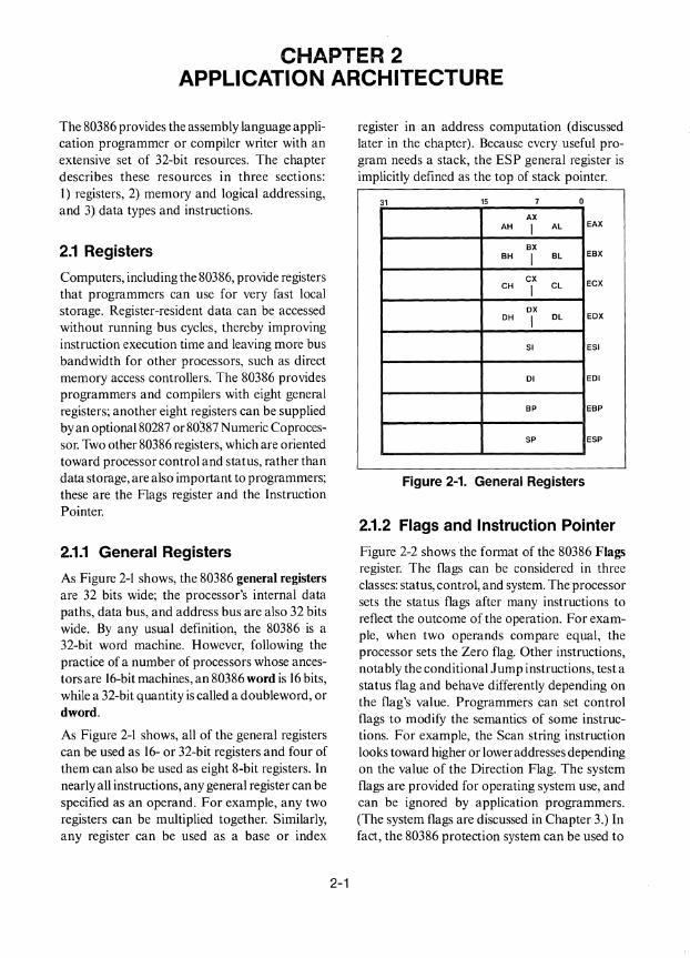
As Figure 2-1 shows, the 80386 general registers are 32 bits wide; the processor's internal data paths, data bus, and address bus are also 32 bits wide. By any usual definition, the 80386 is a 32-bit word machine. However, following the practice of a number of processors whose ancestors are 16-bit machines, an 80386 word is 16 bits, while a 32-bit quantity is called a doubleword, or dword.
As Figure 2-1 shows, all of the general registers can be used as 16- or 32-bit registers and four of them can also be used as eight 8-bit registers. In nearly all instructions, any general register can be specified as an operand. For example, any two registers can be multiplied together. Similarly, any register can be used as a base or index
2-1
register in an address computation (discussed later in the chapter). Because every useful program needs a stack, the ESP general register is implicitly defined as the top of stack pointer.
31 15
AX AH I AL EAX
BX BH I BL EBX
CX CH I CL ECX
OX OH I OL EOX
SI ESI
01 EOI
BP EBP
SP ESP
Figure 2-1. General Registers
2.1.2 Flags and Instruction Pointer
Figure 2-2 shows the format of the 80386 Flags register. The flags can be considered in three classes: status, control, and system. The processor sets the status flags after many instructions to reflect the outcome of the operation. For example, when two operands compare equal, the processor sets the Zero flag. Other instructions, notably the conditional Jump instructions, testa status flag and behave differently depending on the flag's value. Programmers can set control flags to modify the semantics of some instructions. For example, the Scan string instruction looks toward higher or lower addresses depending on the value of the Direction Flag. The system flags are provided for operating system use, and can be ignored by application programmers. (The system flags are discussed in Chapter 3.) In fact, the 80386 protection system can be used to

APPLICATION ARCHITECTURE
prevent application programs from inadvertently altering the system flags.
The 80386 Instruction Pointer, called EIP, is 32 bits wide. The Instruction Pointer controls instruction fetching (including prefetching) and the processor automatically increments it after executing an instruction. Interrupts, exceptions, and control transfer instructions, such as jumps and calls, alter the Instruction Pointer.
2.1.3 Numeric Coprocessor Registers
The numeric coprocessor registers shown in Figure 2-3 improve the performance of numeric applications. Connecting an 80287 or 80387 Numeric Coprocessor to an 80386 effectively
STATUS FLAGS
CARRY
PARITY
AUXILIARY CARRY
ZERO
SIGN
OVERFLOW
I
adds these registers to the 80386. While a numeric coprocessor recognizes integers, packed decimal, and floating point formats of various lengths, internally it holds all values in an eightdeep 80-bit-wide floating point register stack. Numeric instructions may implicitly refer to the top element(s) of the stack, or explicitly to other registers. The Status Register maintains the top of stack pointer, flags that identify exceptions (for example, overflow), and condition codes that reflect the result of the last instruction. The Control Register contains option and mask bits that the programmer can set to select the rounding algorithm, how infinity is to be modeled, and whether exceptions are to be handled by the coprocessor or by software.
I ~ 17 16 15 14 13 12 11 10 9 8 7 6 5 4 3 2 1 0
_ VM I RF ~ NT I 10PL I OF I OF IIF I TF I SF I ZF ~ AF ~ PF ~ CF I
lJ SYSTEM FL AGS
VIRTUAL 86 M ODE
RESUME
NESTED TAS K
1/0 PRIVILEG E LEVEL
INTERRUPTS ENABLED
FLAGS
I CONTROL
DIRECTION
TRAP
Figure 2-2. Flags Register
2-2

APPLICATION ARCHITECTURE
REGISTER STACK
79 78 64 63
± EXPONENT SIGNIFICAND
CONTROL REGISTER
STATUS REGISTER
Figure 2-3. Numeric Coprocessor Registers
2.2 Memory and logical Addressing
80386 application programs use logical addresses to specify the locations of operands in a 4-gigabyte physical address space. The processor automatically translates these logical addresses to the physical addresses that it emits on the system bus. As discussed more fully in Chapter 3, an 80386 operating system can tailor an application program's view of its logical address space. For example, an operating system can define the logical address space as it is defined by many architectures, as a simple array of 232 bytes. Alternatively, an 80386 operating system can organize the logical address space as a collection of variable-length segments. An operating system can define many segments or just a few, as appropriate to its view of logical memory; the 80386 does not dictate the use of segments, but rather allows them to be used as they support application needs. When reading the following sections, bear in mind that the extent to which an
2-3
application program actively uses segments depends on the framework established by the operating system.
2.2.1 Segments
As just mentioned, an operating system can define the 80386 logical address space as one or more segments. Segments are logical units that map well to programming structures, which are inherently variable in length. For example, a l5l6-byte procedure fits exactly into a 1516-byte segment, as an 8-megabyte array (for example, a 1028x1028x8 display buffer) fits exactly into a segment of the same size. By providing architectural support for segments (for example, segments can be individually protected, and can be shared selectively between tasks), the 80386 improves the performance of systems that choose segments as a structuring mechanism. (Pages, which are described in Chapter 3, are fixed-size; they do not map well to programming constructs, but, on the other hand, are better-suited to operating system functions such as swapping.)
An 80386 segment can be any size from 1 byte to 4 gigabytes. For every segment, the operating system maintains an architecture-defined descriptor that specifies the attributes of the segment. Segment attributes include a 32-bit base address and limit (length), and protection information that can guard a segment against incorrect use. Because descriptors are maintained by operating systems, fuller coverage of them is deferred to Chapter 3. Application programs deal only indirectly with descriptors, referring to segments by means of logical addresses.
2.2.2 Logical Addresses
Because a program may potentially refer to multiple segments, an 80386 logical address must identify a segment. Therefore, an 80386 logical address consists of two parts, a 16-bit segment selector and a 32-bit offset into the selected segment (see Figure 2-4). The selector part of a
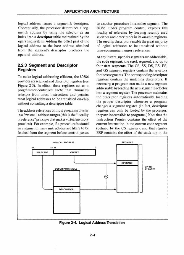
APPLICATION ARCHITECTURE
logical address names a segment's descriptor. Conceptually, the processor determines a segment's address by using the selector as an index into a descriptor table maintained by the operating system. Adding the offset part of the logical address to the base address obtained from the segment's descriptor produces the operand address.
2.2.3 Segment and Descriptor Registers
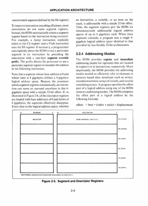
To make logical addressing efficient, the 80386 provides six segment and descriptor registers (see Figure 2-5). In effect, these registers act as a programmer-controlled cache that eliminates selectors from most instructions and permits most logical addresses to be translated on-chip without consulting a descriptor table.
The address references of most programs cluster in a few small address ranges (this is the "locality ofreference"principle that makes virtual memory practical). For example, if a procedure is stored in a segment, many instructions are likely to be fetched from the segment before control passes
LOGICAL ADDRESS
47 32 31
I SELECTOR OFFSET
l DESCRIPTOR TABLE
'--- DESCRIPTOR
0
I
to another procedure in another segment. The 80386, under program control, exploits this locality of reference by keeping recently used selectors and descriptors in its on-chip registers. The on-chip descriptors enable the great majority of logical addresses to be translated without time-consuming memory references.
At any instant, up to six segments are addressable, the code segment, the stack segment, and up to four data segments. The CS, SS, DS, ES, FS, and GS segment registers contain the selectors for these segments. The corresponding descriptor registers contain the matching descriptors. If necessary, a program can make a new segment addressable by loading the new segment's selector into a segment register. The processor maintains the descriptor registers automatically, loading the proper descriptor whenever a program changes a segment register. (In fact, descriptor registers can only be loaded by the processor; they are inaccessible to programs.) Note that the Instruction Pointer contains the offset of the current instruction in the current code segment (defined by the CS register), and that register ESP contains the offset of the stack top in the
SEGMENT -
OPERAND
UP TO 232 BYTES
+
-
Figure 2-4. Logical Address Translation
2-4
APPLICATION ARCHITECTURE
current stack segment (defined by the SS register).
To improve instruction encoding efficiency, most instructions do not name segment registers. Instead, the 80386 automatically selects a segment register based on the instruction being executed. For example, a Jump instruction implicitly refers to the CS register and a Push instruction uses the SS register. If necessary, a programmer can explicitly direct the 80386 to use a particular segment in an instruction by preceding the instruction with a one-byte segment override prefix. The prefix directs the processor to use a particular segment register to translate the address in the following instruction.
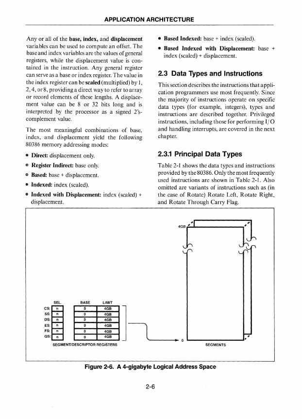
Note that a segment whose base address is 0 and whose limit is 4 gigabytes defines a 4-gigabyte logical address space. Because the processor selects segment registers automatically, an instruction can name an operand anywhere in this 4-gigabyte space with a simple 32-bit offset. If, as illustrated in Figure 2-6, all the descriptor registers are loaded with base addresses of 0 and limits of 4 gigabytes, the segments effectively disappear. Every byte in the logical address space, whether
15 SEGMENT 63
SELECTOR
-ADDITIONAL DESCRIPTOR FIELDS ARE DESCRIBED IN CHAPTER 3.
an instruction, a variable, or an item on the stack, is addressable with a simple 32-bit offset. Thus, the segment registers give the 80386 six instantancously addressable logical address spaces of up to 4 gigabytes each. When these segments coincide, a program sees a single 4-gigabyte logical address space identical to that provided by less-flexible 32-bit architectures.
2.2.4 Addressing Modes
The 80386 provides register and immediate addressing modes for operands that are located in registers or in instructions, respectively. More importantly, the 80386 provides the addressing modes needed to efficiently refer to elements in memory-based data structures such as arrays, records (structures), arrays of records, and records containing arrays. A program spccifies the offset part of a logical address using one of the 80386 memory addressing modes. The 80386 computes the offset part of a logical address by the following formula:
offset: = base + (index * scale) + displacement
DESCRIPTOR
BASE ADDRESS. LIMIT ETC.· CS (CODE)
55 (STACK)
os (DATA)
ES (DATA)
FS (DATAl
GS (DATA)
Figure 2-5. Segment and Descriptor Registers
2-5
APPLICATION ARCHITECTURE
Any or all of the base, index, and displacement variables can be used to compute an offset. The base and index variables are the values of general registers, while the displacement value is contained in the instruction. Any general register can serve as a base or index register. The value in the index register can be scaled (mUltiplied) by I, 2,4, or 8, providing a direct way to refer to array or record elements of these lengths. A displacement value can be 8 or 32 bits long and is interpreted by the processor as a signed 2'scomplement value.
The most meaningful combinations of base, index, and displacement yield the following 80386 memory addressing modes:
• Direct: displacement only.
o Register Indirect: base only.
o Based: base + displacement.
• Indexed: index (scaled).
• Indexed with Displacement: index (scaled) + displacement.
SEL. BASE LIMIT
• Based Indexed: base + index (scaled).
• Based Indexed with Displacement: base + index (scaled) + displacement.
2.3 Data Types and Instructions
This section describes the instructions that application programmers use most frequently. Since the majority of instructions operate on specific data types (for example, integers), types and instructions are described together. Privileged instructions, including those for performing 1/0 and handling interrupts, are covered in the next chapter.
2.3.1 Principal Data Types
Table 2-1 shows the data types and instructions provided by the 80386. Only the most frequently used instructions are shown in Table 2-1. Also omitted are variants of instructions such as (in the case of Rotate) Rotate Left,"Rotate Right, and Rotate Through Carry Flag.
4GB # #1
b
"I 0 4GB
l~. SS: n 4GB
OS: n 4GB
ES: n 0 4GB
FS: n 4GB GS: n 0 4GB 1-7
#
SEGMENT/DESCRIPTOR REGISTERS SEGMENTS
Figure 2-6. A 4-gigabyte Logical Address Space
2-6
APPLICATION ARCHITECTURE
Table 2-1. Principal Data Types and Instructions
Type
Integer, Ordinal
Size
8, 16,32 bits
Unpacked I digit Decimal
Packed 2 digits Decimal
Instructions
Move, Exchange, Translate, Test, Compare, Convert, Shift, Double Shift, Rotate, Not, Negate, And, Or, Exclusive Or, Add, Subtract, Multiply, Divide, Increment, Decrement, Convert (M Dve with sign/ zero extension)
Adjust for: Add, Subtract, Multiply, Divide
Adjust for: Add, Subtract
String (hyte, 0-4G bytes, M ave, Load, Store, word, dword) words, dwords Compare, Scan, Repeat
Bit String
Near Pointer!
1-4G bits
32 bits
Test, Test and Set, Test and Reset, Test and Complement, Scan, Inscrt, Extract
(Samc as Ordinal)
Far Pointer 48 bits Load
I. A near pointer is a 32-bit offset into a segment defined by one of the segment/descriptor register pairs. A far pointer is a full logical addess, that is, a selector and an offset.
Figure 2-7 shows how exam pies of the basic data types are stored in memory, Multibyte items can be located at any byte address. Depending on the bus design, additional bus cycles may be required to access an operand located at an address that is not a multiple of its size. Therefore, for best performance independent of bus design, most programs align word operands on word boundaries, dword operands on doubleword boundaries, and so on.
2.3.2 Numeric Coprocessor Data Types
An 80287 or 80387 Numeric Coprocessor supplements the 80386 with the data types and instructions shown in Table 2-2. Most numeric applications store input values and output results in the integer, real, or packed decimal types and reserve
2-7
the temporary real type for intermediate values, where its extended range and precision minimize rounding, underflow, and overflow problems in complex computations. In accordance with this model, a numeric coprocessor performs most computations on temporary real values stored in its registers. Loading any type into the register stack automatically converts the type to temporary real. A temporary real value in a register can be converted to any other type by a Store instruction.
Table 2-2. Principal Numeric Coprocessor Data Types and Instructions
Type
Integer
Packed Decimal
Real
Temporary Real
Size
16,32, 64 bits
18 digits
32,64 bits
80 bits
Instructions
Load, Store, Compare, Add, Subtract, Multiply, Divide
Load, Store
Load, Store, Compare, Add, Subtract, Multiply, Divide
Add, Subtract, Multiply, Divide, Square Root, Scale Remainder, Integer Part, Change, Sign, Absolute Value, Extract Exponent and Significand, Compare, Examine, Test, Exchange Tangent, Arctangent, 2'-1, y* Log2 (X + 1), y* Log2 (X), Load Constant (0.0, pi, etc.) (80387 adds Sine, Cosine, Sine and Cosine, Unordered Compare)
Figure 2-8 shows how numeric data types are stored in memory.
2.3.3 Other Instructions
Not all 80386 instructions are associated with data types. The following paragraphs survey the untyped instructions.
2.3.3.1 Stack Instructions
An 80386 stack is a stack of dwords whose base and top are defined by the SS and ESP
APPLICATION ARCHITECTURE
registers, respectively. The Push instruction pushes a dword onto the stack and the Pop instruction pops the top d word from the stack into a register or to memory. Push All pushes the general registers onto the stack and Pop All does the reverse.
The Enter and Leave instructions are provided for block-structured high-level languages. The Enter instruction builds the stack frame and display that compilers use to link procedure calls. The Leave instruction removes the display and stack frame from the stack in preparation for returning to the calling procedure.
" INCREASING SIGNIFICANCE
2.3.3.2 Control Transfer Instructions
The Jump instruction transfers control to another instruction by changing the value of the Instruction Pointer. The target instruction may be in the same code segment (up to 232
bytes a way) or in a different one. The operand of an intrasegment Jump is a near pointer, that is, the offset of the target instruction in the current code segment; thus, a Jump can be directed to any location in the largest possible segment. The operand of an intersegment Jump is a far pointer. allowing control to be
I RELATIVE ADDRESSES
7 0 o BYTE ORDINAL
MAGNITUDE ___ -It
47
~ 0
... IIL-__________ ..... I DWORD INTEGER
t,--I ----MAGNITUDE------'
'-------SIGN
7 0 o UNPACKED DECIMAL
7 3 0 OJ PACKED DECIMAL
d~.,...I ____ -------.-1 BYTE STRING
LEFTMOST BYTE------'t
~ 0
1L-__________ -.l1 NEAR POINTER
31 I FAR POINTER L-______ ~ ____________ ~
L SELECTOR ~~I---- OFFSET - ___ ~
Figure 2-7. Data Type Storage
2-8
APPLICATION ARCHITECTURE
transfered to any point in a segment. (The selector part of the far pointer replaces the value in the CS register while the offset part replaces the value in EIP) A full set of conditional Jump instructions, which branch based on the value of a status flag, is also available; these instructions can also transfer to locations up to 232 bytes away.
Procedures and functions (subroutines) can be invoked with the Call instruction and a called routine can return with the Return instruction. As with Jumps, Calls within a code segment have near pointer operands which specify a new value for the Instruction Pointer, while Calls to a different code segment have far pointer operands that change the CS register in addition to EIP. Call instructions push the address of the following instruction
onto the stack and then load the Instruction Pointer (and the CS register, if the transfer is to a different segment). The Return instruction pops the saved value(s) from the stack into Erp, and CS, if applicable. Calls can be indefinitely nested and recursive, subject only to the size of the stack.
For controlling loops, the 80386 provides the Loop and conditional Loop instructions in addition to conditional Jumps. The loop instructions use the ECX register as a repetition counter; they decrement ECX and terminate the loop when the register's value becomes zero. The conditional Loop instructions terminate a loop prematurely when a flag takes a specified value. While the Loop instructions are designed for "bottom of loop" testing, adding a Jump If ECX Zero instruction
I RELATIVE ADDRESSES
... "'f----- INCREASING SIGNIFICANCE
79 71 3 0
(G::::J I I I I I PACKED DECIMAL
Q ... 'S-IG-N--------MAGNITUDE-----------'
31 23 0
... 11--. ............ ________ 1 SHORT REAL l' • II MAGNITUDE----....J
BIASED EXPONENT
SIGN
63 51 0
LJIIL-_-LI ____________ ---JILONG REAL
~II MAGNITUDE
t BIASED EXPONENT
SIGN
79 62 0
.. I &..1 ___ --11 ... 11 _________________ ---11 TEMPORARY REAL
tL.1 _--,-_---ll L.I -------MAGNITUDE l t ____ BIASED EXPONENT
L-.-----SIGN
Figure 2-8. Numeric Coprocessor Data Type Storage Examples
2-9

APPLICATION ARCHITECTURE
implements a "top of loop" test that allows the loop to be executed zero times.
2.3.3.3 Miscellaneous Instructions
The 80386 Bound instruction can be used to verify that an array subscript is within the bounds of the array. There are instructions for setting and clearing flags, and for loading and storing the status byte of the Flags register. The 80287 and 80387 supply the instructions that an operating system needs to initialize the coprocessor, handle coprocessor exceptions, and save and restore the coprocessor's state. Finally, of course, the 80386 has a No Operation instruction.
2-10

Chapter 3 System Architecture
3

CHAPTER 3 SYSTEM ARCHITECTURE
The purpose of a system architecture is to support operating systems, but operating systems are quite diverse in their needs. In response, the 80386 provides an array of resources that operating system designers and implementors can selectively employ. In effect, the 80386 system architecture can be configured to fit the needs of the operating system under development.
3.1 System Registers
In addition to the registers described in the preceding chapter, an operating system sometimes uses the 80386 registers shown in Figure 3-1. (Later sections of this chapter sometimes refer to these registers, so they are shown here for reference.) In the main, it is the 80386 that uses the system registers; the operating system initializes the system registers and then ignores them during normal operation. The operating system may, however, use a system register to handle an exception. For example, when a page fault occurs, the processor loads the faulting address into CR2; the operating system's page fault handler uses the address to find the associated page table entry. The system registers are normally inaccessible to application programs,
47
BASE ADDRESS
63
I SELECTOR
I SYSTEM ADDRESS REGISTERS
31
15
since only privileged instructions can operate on them. (Exceptions, page faults, and privileged instructions are explained later in this chapter.)
3.2 Multitasking
Many of the 80386's system architecture facilities directly support multitasking operating systems, though, of course, the 80386 can be used in demanding single-task applications. Multitasking is a technique for managing a computer system's work when that work consists of multiple activities; three such activities might be editing one file, compiling another, and transmitting a third to another computer. In a multitasking system, each activity that can proceed in parallel with other activities is represented by a task. (In this introduction, the term "task" is considered equivalent to the term "process.") Each task executes a program consisting of instructions and initial data values. More than one task can execute the same program; for example, in a timesharing multitasking system several tasks (each corresponding to a user) commonly execute the same compiler or editor. Programs and tasks are related in somewhat the same way that sheet music and musical performances are related: a
LIMIT GDTR: GLOBAL DESCRIPTOR TABLE
IDTR: INTERRUPT DESCRIPTOR TABLE
LDTR: LOCAL DESCRIPTOR TABLE
TR: RUNNING TASK'S TSS
CRO: OPTIONS (FOR EXAMPLE, PAGING)
~--------------~ CR1: (RESERVED BY INTEL)
CR2: PAGE FAULT LINEAR ADDRESS
CR3: PAGE DIRECTORY BASE ADDRESS
SYSTEM CONTROL REGISTERS
Figure 3-1. System Registers
3-1
SYSTEM ARCHITECTURE
program is a text that describes an algorithm, and a task is one execution (performance) ofthat algorithm.
The programs that tasks execute are designed as though they were to run on dedicated processors sharing a common memory; that is, except ror occasional pauses to communicate or synchronize with other tasks, a task theoretically runs continuously in parallel with all other tasks. In fact, however, the tasks run one at a time in short bursts on a single processor.
The multitasking operating system simulates mUltiple processors by providing each task with a "virtual processor." At any instant, the operating system assigns the real processor to one of the virtual processors, thereby running the associated task. To maintain the illusion of one processor per task, the operating system frequently switches the real processor to a different virtual processor. The 80386 system architecture supports this critical task switch operation with Task State Segments and instructions that switch tasks.
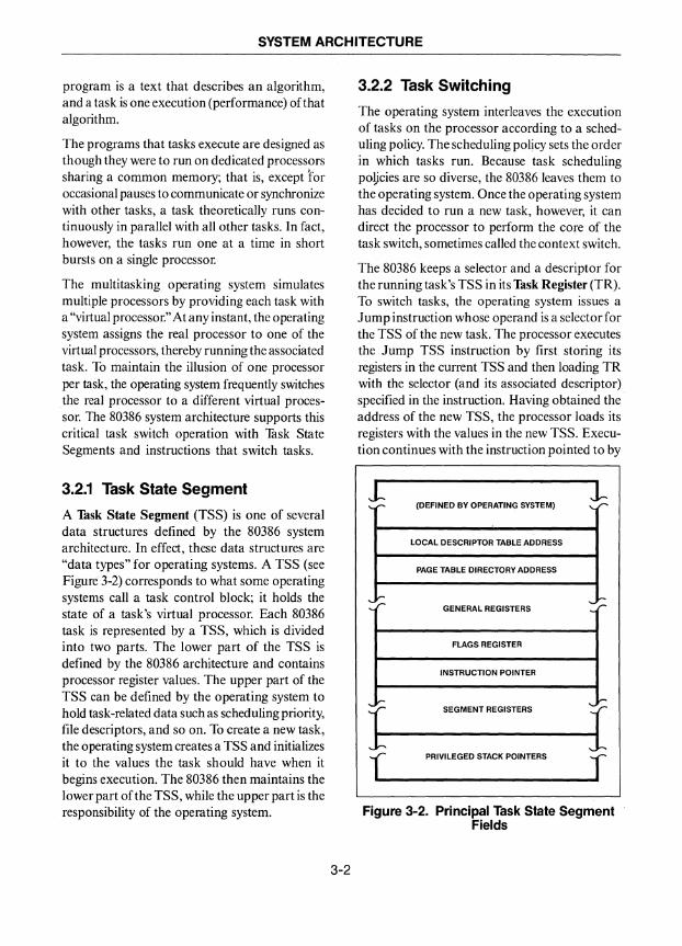
3.2.1 Task State Segment
A Task State Segment (TSS) is one of several data structures defined by the 80386 system architecture. In effect, these data structures are "data types" for operating systems. A TSS (see Figure 3-2) corresponds to what some operating systems call a task control block; it holds the state of a task's virtual processor. Each 80386 task is represented by a TSS, which is divided into two parts. The lower part of the TSS is defined by the 80386 architecture and contains processor register values. The upper part of the TSS can be defined by the operating system to hold task-related data such as scheduling priority, file descriptors, and so on. To create a new task, the operating system creates a TSS and initializes it to the values the task should have when it begins execution. The 80386 then maintains the lower part of the TSS, while the upper part is the responsibility of the operating system.
3-2
3.2.2 Task Switching
The operating system interleaves the execution of tasks on the processor according to a scheduling policy. The scheduling policy sets the order in which tasks run. Because task scheduling poljcies are so diverse, the 80386 leaves them to the operating system. Once the operating system has decided to run a new task, however, it can direct the processor to perform the core of the task switch, sometimes called the context switch.
The 80386 keeps a selector and a descriptor for the running task's TSS in its Task Register (TR). To switch tasks, the operating system issues a Jump instruction whose operand is a selector for the TSS of the new task. The processor executes the Jump TSS instruction by first storing its registers in the current TSS and then loading TR with the selector (and its associated descriptor) specified in the instruction. Having obtained the address of the new TSS, the processor loads its registers with the values in the new TSS. Execution continues with the instruction pointed to by
1 l-.. -- (DEFINED BY OPERATING SYSTEM) ,roo
LOCAL DESCRIPTOR TABLE ADDRESS
PAGE TABLE DIRECTORY ADDRESS
.. ~ GENERAL REGISTERS
~ ~
FLAGS REGISTER
INSTRUCTION POINTER
.. '" .... --SEGMENT REGISTERS
I PRIVILEGED STACK POINTERS r
Figure 3-2. Principal Task State Segment Fields

SYSTEM ARCHITECTURE
the new task's Instruction Pointer. To later resume execution of the old task, the operating system issues a Jump TSS to the old task's TSS; execution of the old task then continues with the instruction following the Jump TSS that suspended the task. The task switch described here takes 17 microseconds (16 M Hz., no wait states).
3.3 Addressing
The physical address space of most computers is organized as a simple array of bytes. With the development of memory management units (M MUs), computer architectures began to distinguish between the physical address space implemented by the memory hardware and the logical address space seen by a programmer. The M M U translates the logical addresses presented by programs into the physical addresses that go out on the bus. Most architectures view a task's logical address space as consisting of a collection of one of the following:
Bytes
Segments
Pages
The logical address space consists of an array of bytes with no other structure (this is sometimes called a "flat" or "linear" address space). NoM M U translation is required because a logical address is exactly equivalent to a physical address.
The logical address space consists of a few or many segments, each of which is composed of a variable number of bytes. A logical address is given in two parts, a segment number and an offset into the segment. The MMU translates a logical address into a physical address.
The logical address space consists of many pages, each of which is composed of a fixed number of bytes. A logical address is a page number plus
3-3
an offset within the page. The MMU translates a logical address into a physical address.
Paged Segments The logical address space consists of segments which themselves consist of pages. A logical address is a segment number and an offset. The MMU translates the logical address into a page number and an offset and then translates these into a physical address.
Each of these views matches some classes of system well and others less well. For example, the "flat" view is appropriate for simple embedded systems, while systems that separately manage and protect individual program structures fit better with the segmented view of memory. Technically, the 80386 views memory as a collection of segments that are optionally paged. In practice, the 80386 architecture supports operating systems that use any of the four views of memory described above.
3.3.1 Address Translation Overview
Figure 3-3 shows the fundamentals of 80386 logical-to-physical address translation. The sequence of operations shown in Figure 3-3 is central to both addressing and protection. It is described here in skeleton form to clearly establish its overall outline before considering such features as virtual memory and protection. Subsequent sections elaborate on the translation stages and show how they can be tailored to fit the needs of a particular system.
As described in the previous chapter, the 80386 memory addressing modes yield the 32-bit offset ofthe target operand. Combined with a segment selector, this offset forms a two-part logical address: the selector identifies the target segment and the offset locates the operand in the segment. In the vast majority of instructions, the selector is specified implicitly as the content of a segment register.
SYSTEM ARCHITECTURE
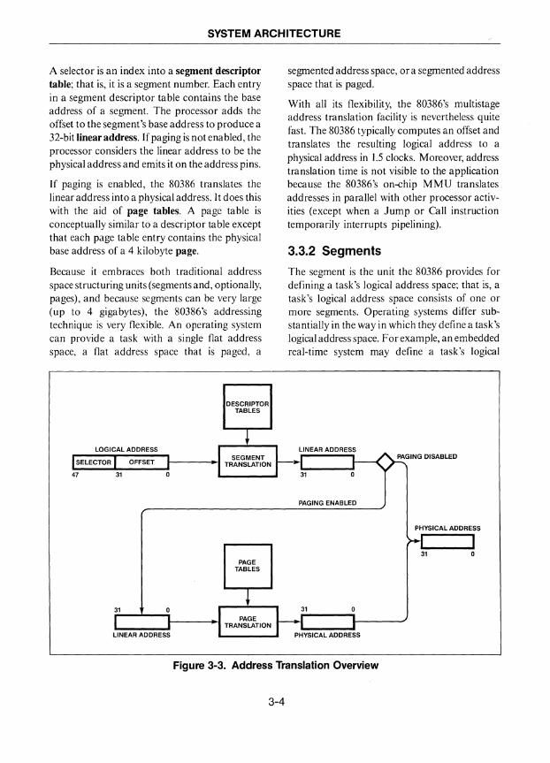
A selector is an index into a segment descriptor table; that is, it is a segment number. Each entry in a segment descriptor table contains the base address of a segment. The processor adds the offset to the segment's base address to produce a 32-bit linear address. If paging is not enabled, the processor considers the linear address to be the physical address and emits it on the address pins.
If paging is enabled, the 80386 translates the linear address into a physical address. It does this with the aid of page tables. A page table is conceptually similar to a descriptor table except that each page table entry contains the physical base address of a 4 kilobyte page.
Because it embraces both traditional address space structuring units (segments and, optionally, pages), and because segments can be very large (up to 4 gigabytes), the 80386's addressing technique is very flexible. An operating system can provide a task with a single flat address space, a flat address space that is paged, a
LOGICAL ADDRESS
OFFSET
31
LINEAR ADDRESS
DESCRIPTOR TABLES
PAGE TABLES
segmented address space, or a segmented address space that is paged.
With all its flexibility, the 80386's multistage address translation facility is nevertheless quite fast. The 80386 typically computes an offset and translates the resulting logical address to a physical address in 1.5 clocks. Moreover, address translation time is not visible to the application because the 80386's on-chip MMU translates addresses in parallel with other processor activities (except when a Jump or Call instruction temporarily interrupts pipelining).
3.3.2 Segments
The segment is the unit the 80386 provides for defining a task's logical address space; that is, a task's logical address space consists of one or more segments. Operating systems differ substantially in the way in which they define a task's logical address space. For example, an embedded real-time system may define a task's logical
PAGING ENABLED
PHYSICAL ADDRESS
Figure 3-3. Address Translation Overview
3-4
SYSTEM ARCHITECTURE
address space to be a single entity shared by all tasks and the operating system itself; in other words, a single segment is shared system-wide. At the other extreme, a system might map every data structure and procedure into a different segment, making a task's logical address space consist of dozens or hundreds of address spaces, each corresponding to a procedure or a data structure. Between these extremes might fall a general-purpose timesharing system in which tasks run in separate logical address spaces, and in which a task's code is separated from its data, and application code and data are separated from operating system code and data. The 80386 segmentation facility is versatile enough to support each ofthese examples, and others as well.
As described in Chapter 2, an instruction refers to a memory operand by a two-part logical address consisting of a segment selector and an offset into the segment. In principle, the 80386 translates the logical address to a linear address by using the selector to look up the segment's descriptor in a segment descriptor table. The descriptor contains the segment's base address in the linear address space; adding the offset produces the operand's linear address. In practice, the logical-to-linear address translation is optimized by implicit selectors and register-based descriptors. As a result, the descriptor table lookup only occurs for instructions that load
ATTRIBUTES ACCESSED
RIGHTS
TYPE
PRIVILEGE
PRESENT
I ~
LIMIT
new selectors into segment registers (for example, a Call to a procedure in a different segment changes the selector in the CS register).
I
Although it rarely occurs in practice, it is nevertheless convenient to think of the processor translating logical addresses by looking up descriptors in segment descriptor tables because it follows that the descriptors in a task's segment descriptor tables define the task's logical address space. Without a descriptor a task has no way to generate a linear address.
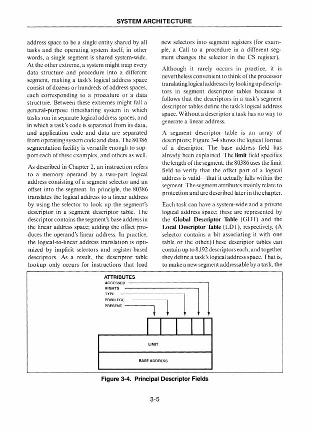
A segment descriptor table is an array of descriptors; Figure 3-4 shows the logical format of a descriptor. The base address field has already been explained. The limit field specifies the length ofthe segment; the 80386 uses the limit field to verify that the offset part of a logical address is valid-that it actually falls within the segment. The segment attributes mainly relate to protection and are described later in the chapter.
Each task can have a system-wide and a private logical address space; these are represented by the Global Descriptor Table (GOT) and the Local Descriptor Table (LOT), respectively. (A selector contains a bit associating it with 'one table or the other.)These descriptor tables can contain up to 8,192 descriptors each, and together they define a task's logical address space. That is, to make a new segment addressable by a task, the
1 I I I I I I
BASE ADDRESS
Figure 3-4. Principal Descriptor Fields
3-5
SYSTEM ARCHITECTURE
operating system must insert a descriptor for the segment into the G DT or into the task's LDT. In protected systems, the G DT and LDT can be made privileged structures so that only the operating system can modify them.
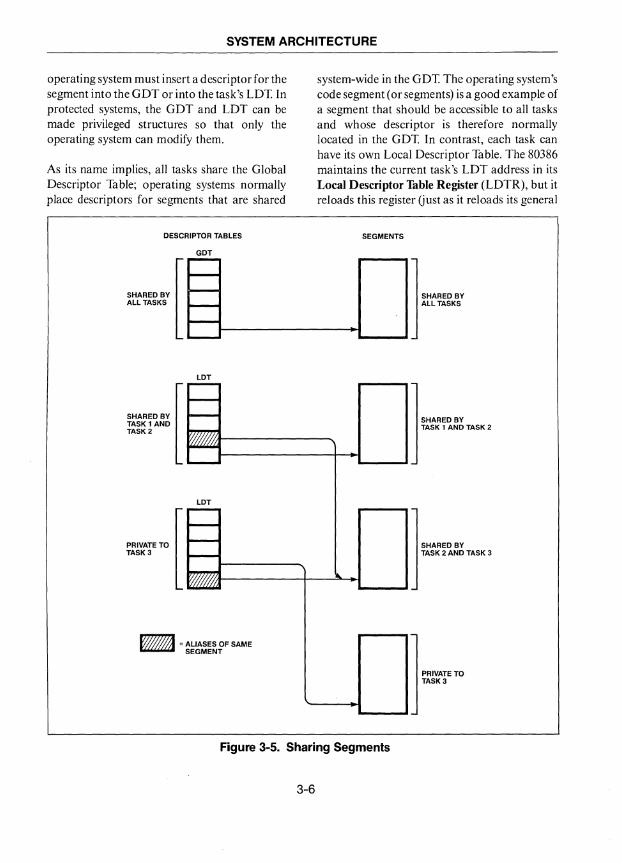
As its name implies, all tasks share the Global Descriptor Table; operating systems normally place descriptors for segments that are shared
DESCRIPTOR TABLES
GOT
system-wide in the GDT. The operating system's code segment (or segments) is a good example of a segment that should be accessible to all tasks and whose descriptor is therefore normally located in the GDT. In contrast, each task can have its own Local Descriptor Table. The 80386 maintains the current task's LDT address in its Local Descriptor Table Register (LDTR), but it reloads this register (just as it reloads its general
SEGMENTS
:~~~' [~~.I I}~:~~' LOT
,~'"'' [ TASK 1 AND TASK 2
I----------+-.... L-__ ...... ] ~t:~:: ,~., LOT
PRIVATE TO [ TASK 3
Ii;'7ii77JiI = ALIASES OF SAME ~ SEGMENT
'----... L-__ ...... ] I:l'tl'ro
Figure 3-5. Sharing Segments
3-6
SYSTEM ARCHITECTURE
and segment registers) from the new task's TSS on task switches.
Tasks may share a segment in three ways (see Figure 3-5):
1. A segment whose descriptor is in the GDT is shared by all tasks.
2. Tasks that share an LOT share the segments described in the LOT; this approach is appropriate for closely cooperating tasks.
3. Descriptors in different LOTs may point to the same segment; such descriptors are called aliases. Aliases allow the unit of intertask sharing to be an individual segment, rather than all segments in a descriptor table.
3.3.3 Pages
Whether a task's logical address space consists of one segment or many, an operating system can subdivide the linear address space into pages. To an operating system, pages are convenient units for allocation and relocation because they are all the same size. Pages also provide a way to protect portions of large segments and, importantly, provide a convenient unit for implementing virtual memory. These applications of paging are discussed in subsequent sections.
An 80386 page is 4K bytes long. This size is consistent with the industry trend toward larger pages and it helps performance in two ways. First, it provides a high page cache hit ratio given the cache size that can reasonably be implemented on-chip with current technology. (The 80386's on-chip page cache is described shortly). Second, 4K bytes is an efficient unit for disk transfer; most operating systems running on machines with smaller page sizes must group pages into "clusters" to keep the number of disk transfers acceptably low.
An 80386 operating system enables paging by setting the PG (Paging Enabled) bit in Control Register 0 with a privileged instruction. When paging is enabled, the processor translates a
3-7
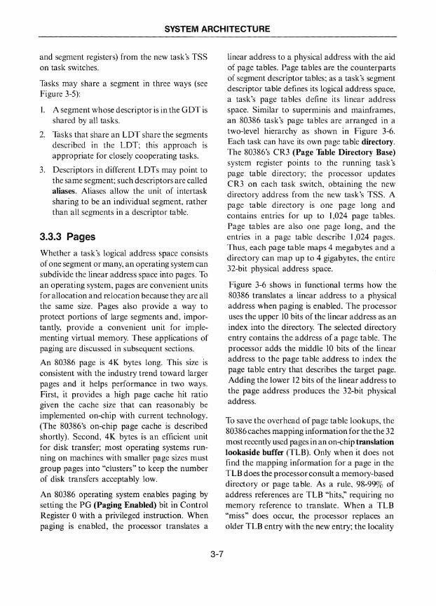
linear address to a physical address with the aid of page tables. Page tables are the counterparts of segment descriptor tables; as a task's segment descriptor table defines its logical address space, a task's page tables define its linear address space. Similar to superminis and mainframes, an 80386 task's page tables are arranged in a two-level hierarchy as shown in Figure 3-6. Each task can have its own page table directory. The 80386's CR3 (Page Table Directory Base) system register points to the running task's page table directory; the processor updates CR3 on each task switch, obtaining the new directory address from the new task's TSS. A page table directory is one page long and contains entries for up to 1,024 page tables. Page tables are also one page long, and the entries in a page table describe 1,024 pages. Thus, each page table maps 4 megabytes and a directory can map up to 4 gigabytes, the entire 32-bit physical address space.
Figure 3-6· shows in functional terms how the 80386 translates a linear address to a physical address when paging is enabled. The processor uses the upper 10 bits of the linear address as an index into the directory. The selected directory entry contains the address of a page table. The processor adds the middle 10 bits of the linear address to the page table address to index the page table entry that describes the target page. Adding the lower 12 bits of the linear address to the page address produces the 32-bit physical address.
To save the overhead of page ta ble lookups, the 80386 caches mapping information for the the 32 most recently used pages in an on-chip translation lookaside buffer (TLB). Only when it does not find the mapping information for a page in the TLB does the processor consult a memory-based directory or page table. As a rule, 98-99% of address references are TLB "hits," requiring no memory reference to translate. When a TLB "miss" does occur, the processor replaces an older TLB entry with the new entry; the locality
SYSTEM ARCHITECTURE
of reference principle suggests that the new entry is likely to be used again in the near future.
While enabling paging does not increase address translation time, it does make instruction execution time vary slightly, due to the occasional TLB misses. By disabling paging, real-time systems can eliminate this potential response time variable.
Figure 3-7 shows the basic content of a page table entry (PTE). Directory entries are identical, except that the page address field is interpreted as the physical address of a page table, rather than a page.
Tasks can share individual pages or entire page tables. Entries in different page tables that point to the same page are aliases of one another just as descriptors with the same base address are aliases of one another. The 80386's two-level page table structure makes it easier to share pages between tasks by sharing entire page tables. Since the
liNEAR ADDRESS
31 21
DIRECTORY PAGE
J
11
.Jl
address of a page shared in this way exists in a single page table, the operating system has one page table entry to update when it moves the page.
3.3.4 Virtual Memory
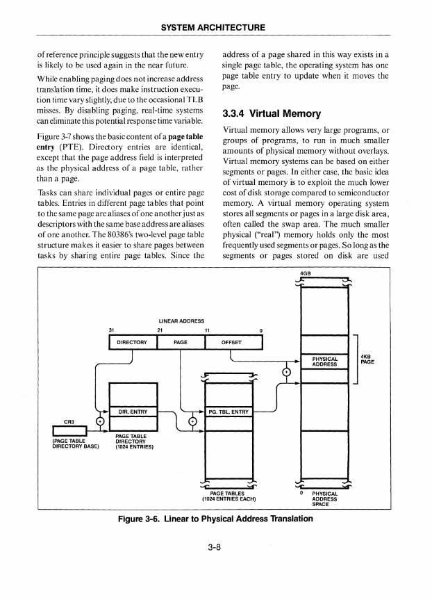
Virtual memory allows very large programs, or groups of programs, to run in much smaller amounts of physical memory without overlays. Virtual memory systems can be based on either segments or pages. In either case, the basic idea of virtual memory is to exploit the much lower cost of disk storage compared to semiconductor memory. A virtual memory operating system stores all segments or pages in a large disk area, often called the swap area. The much smaller physical ("real') memory holds only the most frequently used segments or pages. So long as the segments or pages stored on disk are used
4GB
0
OFFSET J l PHYSICAL
~ ADDRESS
:J:: ]
4KB PAGE
~ DIR. ENTRY n'-f PG. TBl. ENTRY ~
CR3
I (PAGE TABLE DIRECTORY BASE)
PAGE TABLE DIRECTORY (1024 ENTRIES)
~ ~
""'1: :....f'"
PAGE TABLES (1024 ENTRIES EACH)
.... .... ... '-'C >r
o PHYSICAL ADDRESS SPACE
Figure 3-6. Linear to Physical Address Translation
3-8

SYSTEM ARCHITECTURE
infrequently, a virtual memory system will perform nearly as well as one with far more memory at a fraction of the cost. The key architectural features needed to efficiently support virtual memory are:
o A bit for each segment or page that tells the processor (or memory management unit) if the segment or page is "present" in memory or needs to be swapped in from disk.
o A trap or exception mechanism by which the processor can notify the operating system to swap in a not-present segment or page.
o Restartable instructions that enable the processor to retry an instruction after the operating system has loaded the formerly not-present page into memory and marked it present.
The 80386 has all of these necessary facilities, plus others that improve the efficiency of virtual memory management. Both descriptors and page table entries have a Present bit, and therefore can be used as the basis of a virtual memory design. Swapping segments between memory and disk is a reasonable approach when
ATTRIBUTES
the segments are relatively small as they are in l6-bit architectures. When segments can be very large, as they can on the 80386, swapping pages is usually a more effective approach, due to the fixed size of pages. In a page-based system, the operating system allocates and frees memory in page-sized units called page frames; a page swapped in from disk will fit into any available frame. Because most 32-bit virtual memory systems are page-based, the remainder of this section describes the 80386's page-based virtual memory support.
In general, a page-based virtual memory operating system transfers not-present pages from disk to page frames on demand, that is, when notified by the processor that an instruction refers to a not-present page. When the number offree page frames runs low, the operating system also transfers pages from page frames to disk, attempting to remove the pages that are least likely to be referenced in the near future. By transparently swapping pages between page frames and disk, the operating system gives application software the illusion of a physical memory that is as large as the swap area on the disk. The details of these operations are described below.
PRESENT ----------------------,
RIGHTS--------------------,
PRIVILEGE------------------,
ACCESSED--------------, I :::.-D-EF-IN-E-D-)--------l--~l I
PAGE ADDRESS I I I I I I Figure 3-7. Principal Page Table Entry Fields
3-9
SYSTEM ARCHITECTURE
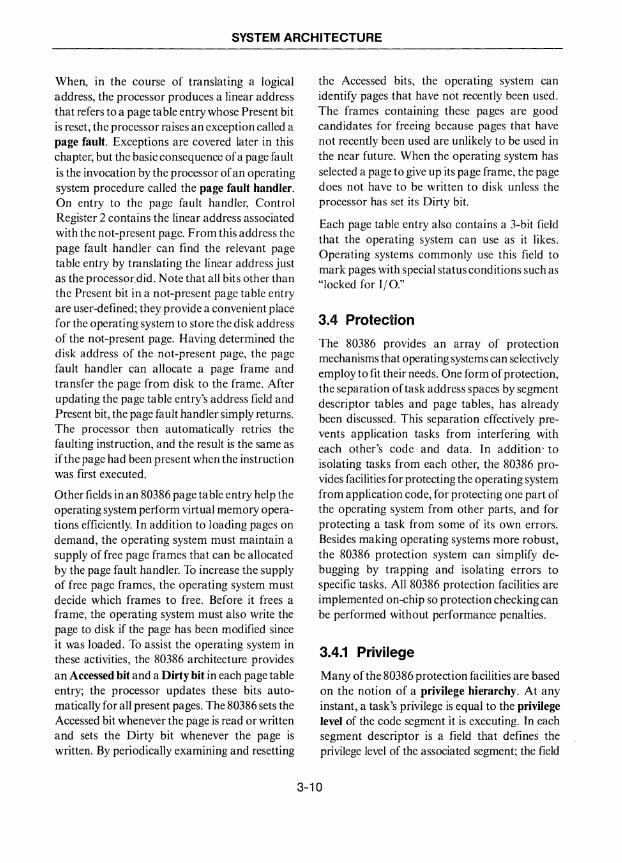
When, in the course of translating a logical address, the processor produces a linear address that refers to a page table entry whose Present bit is reset, the processor raises an exception called a page fault. Exceptions are covered later in this chapter, but the basic consequence of a page fault is the invocation by the processor of an operating system procedure called the page fault handler. On entry to the page fault handler, Control Register 2 contains the linear address associated with the not-present page. From this address the page fault handler can find the relevant page table entry by translating the linear address just as the processor.did. Note that all bits other than the Present bit in a not-present page table entry are user-defined; they provide a convenient place for the operating system to store the disk address of the not-present page. Having determined the disk address of the not-present page, the page fault handler can allocate a page frame and transfer the page from disk to the frame. After updating the page table entry's address field and Present bit, the page fault handler simply returns. The processor then automatically retrics the faulting instruction, and the result is the same as if the page had been present when the instruction was first executed.
Other fields in an 80386 page ta ble entry hel p the operating system perform virtual memory operations efficiently. In addition to loading pages on demand, the operating system must maintain a supply offree page frames that can be allocated by the page fault handler. To increase the supply of free page frames, the operating system must decide which frames to free. Before it frees a frame, the operating system must also write the page to disk if the page has been modified since it was loaded. To assist the operating system in these activities, the 80386 architecture provides an Accessed bit and a Dirty bit in each page table entry; the processor updates these bits automatically for all present pages. The 80386 sets the Accessed bit whenever the page is read or written and sets the Dirty bit whenever the page is written. By periodically examining and resetting
the Accessed bits, the operating system can identify pages that have not recently been used. The frames containing these pages are good candidates for freeing because pages that have not recently been used are unlikely to be used in the near future. When the operating system has selected a page to give up its page frame, the page does not have to be written to disk unless the processor has set its Dirty bit.
Each page table entry also contains a 3-bit field that the operating system can use as it likes. Operating systems commonly use this field to mark pages with special status conditions such as "locked for 1/0."
3.4 Protection
The 80386 provides an array of protection mechanisms that operating systems can selectively employ to fit their needs. One form of protection, the separation of task address spaces by segment descriptor tables and page tables, has already been discussed. This separation effectively prevents application tasks from interfering with each other's code and data. In addition' to isolating tasks from each other, the 80386 provides facilities for protecting the operating system from application code, for protecting one part of the operating system from other parts, and for protecting a task from some of its own errors. Besides making operating systems more robust, the 80386 protection system can simplify debugging by trapping and isolating errors to specific tasks. All 80386 protection facilities are implemented on-chip so protection checking can be performed without performance penalties.
3.4.1 Privilege
Many of the 80386 protection facilities are based on the notion of a privilege hierarchy. At any instant, a task's privilege is equal to the privilege level of the code segment it is executing. In each segment descriptor is a field that defines the privilege level of the associated segment; the field
3-10
SYSTEM ARCHITECTURE
may take one of four values. Privilege level 0 is the most-privileged level and privilege level 3 is the least-privileged level.
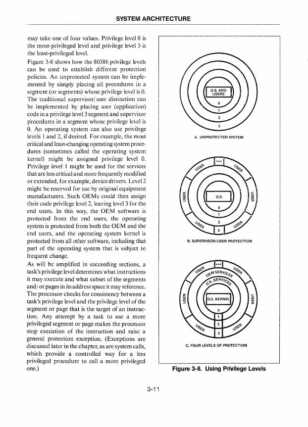
Figure 3-8 shows how the 80386 privilege levels can be used to establish different protection policies. An unprotected system can be implemented by simply placing all procedures in a segment (or segments) whose privilege level is o. The traditional supervisor/ user distinction can be implemented by placing user (application) code in a privilege level 3 segment and supervisor procedures in a segment whose privilege level is O. An operating system can also use privilege levels I and 2, if desired. For example, the most critical and least-changing operating system procedures (sometimes called the operating system kernel) might be assigned privilege level o. Privilege level I might be used for the services that are less critical and more frequently modified or extended, for example, device drivers. Level 2 might be reserved for use by original equipment manufacturers. Such OEMs could then assign their code privilege level 2, leaving level 3 for the end users. In this way, the OEM software is protected from the end users, the operating system is protected from both the OEM and the end users, and the operating system kernel is protected from all other software, including that part of the operating system that is subject to frequent change.
As will be amplified in succeeding sections, a task's privilege level determines what instructions it may execute and what subset of the segments and/ or pages in its address space it may reference. The processor checks for consistency between a task's privilege level and the privilege level of the segment or page that is the target of an instruction. Any attempt by a task to use a more privileged segment or page makes the processor stop execution of the instruction and raise a general protection exception. (Exceptions are discussed later in the chapter, as are system calls, which provide a controlled way for a less privileged procedure to call a more privileged one.)
3-11
A. UNPROTECTED SYSTEM
B. SUPERVISOR/USER PROTECTION
C. FOUR LEVELS OF PROTECTION
Figure 3-8. USing Privilege Levels
SYSTEM ARCHITECTURE
3.4.2 Privileged Instructions
In addition to defining which segments and pages it can use, a task's privilege level defines the instructions it can execute. The 80386 has a number of instructions whose execution must be tightly controlled to prevent serious system disruption. All of the instructions that load new values into the system registers are examples of privileged instructions. Only a task running at privilege level 0 can execute privileged instructions,
3.4.3 Segment Protection
The descriptors in a task's LDTand GDT define the task's logical address space. The segments defined in these tables are theoretically addressable, because the descriptor tables provide the information necessary to compute a segment's address. However, an addressable segment may not be accessible to a particular operation because of the additional protection checks made by the 80386. The 80386 checks every segment reference (whether generated by the execution of an instruction or an instruction fetch) to verify that the reference is consistent with the protection attributes of the segment as described below.
Privilege To access a segment, a program must be at least as privileged as the segment. For example, a program running at level 3 can only reference segments whose privilege level is also 3, while a program running at level 0 can access all segments in its logical address space.
Limit A reference to a segment must fall within the segment's limit. Segment limits enable the processor to trap common programming errors such as stack overflow, bad pointers and array subscripts, and bad call and jump addresses. In cases where the operating system can determine that
3-12
Type
Rights
a reference outside the bounds of a segment is not an error (stack overflow is an example in some systems), the operating system can extend the segment (for example, by adding a page to it) and restart the instruction.
Each descriptor contains a type field that the processor checks for consistency with the instruction it is exccuting. Ordinary segments have a type of code or data, ena bling the processor to catch an attempt to overwrite code, for example, the segment types manipulated directly by applications are code and data. System descriptors are also typed so the processor can verify when it is switching tasks, for example, that the segmcnt named in Jump TSS instruction is in fact a Task State Segment.
A segment descriptor can be marked with rights that restrict the operations permitted on the associated segment. Code segments can be marked executable or executable-and-readable. Data segments can be marked readonly or readable-and-writable.
All ofthe checks described above depend on the integrity of descriptors. If a task executing its application code could change a descriptor, the checks would guarantee nothing. For this reason, an operating system can restrict access to descriptor tables to privilege level 0 code.
Note that for sharing, different descriptors for the same segment (that is, aliases) may have different protection attributes, allowing, for example, one task to read and write a segment while another can only read it. Aliases also permit the operating system to override the protection system when necessary, for example, to move a code segment.

SYSTEM ARCHITECTURE
3.4.4 Page Protection
Systems that do not make extensive use of segments can instead protect pages. (Page protection can also be applied to sections of large segments.) Like a descriptor, a page table entry has a set of protection attributes; the 80386 checks every reference to the page for conformance to these attributes.
A page table entry can be marked with one of two privilege levels, user or supervisor. User level corresponds to privilege level 3 but supervisor pages can only be accessed by tasks running at privilege levels 0, I, or 2. A user page can also be marked read-only or readable-and-writable.
The 80386 checks a page's protection attributes after verifying that an access is consistent with the segment attributes. Thus, page protection is a convenient way for an operating system to apply additional protection to portions of a segment. For example, an operating system can safely store task-related operating system data, such as page tables and file descriptors, in a task's data segment by making the containing pages superVISor pages.
3.5 System Calls
Most operating systems organize their services as a collection of procedures that tasks can call. An unprotected 80386 operating system can place its procedures and application code in a level 0 code segment (or more than one such segment); an application task can then invoke an operating system service with an ordinary Call instruction. Such an approach is fast but relies on the application tasks to be error-free and wellbehaved (as they are in embedded systems, for example). Nothing prevents a task running at level 0 from calling an address that is not an operating system entry point; nor is such a task prevented from corrupting operating system data. To protect the operating system, application code and data can be placed in less-privileged privileged segments. Just as a task running at a
3-13
given privilege level cannot read or write a more privileged data segment or page, neither can a task directly call a more privileged code segment.
To allow a task executing a less-privileged code segment to make a protected system call, the operating system must define one or more entry points. In the 80386, these entry points are called gates (see Figure 3-9). There are two types of gates that can be used to implement operating system entry points, trap gates and call gates. The two gates are generally similar, but the call gate allows the operating system interface to be identical to that of an ordinary procedure. Using call gates, compilers and assembly language programmers can use a single set of conventions to call any procedure, letting the 80386 take care of the extra processing required to change privilege levels.
ATTRIBUTES
DWORD COUNP n TYPE~ PRIVILEGE 1 PRESENT 1
11 I I ENTRY POINT SELECTOR
ENTRY POINT OFFSET
'DWORD COUNT APPLIES ONLY TO CALL GATES.
Figure 3-9. Principal Gate Fields
As shown in Figure 3-9, a gate contains the logical address of an entry point and a set of attributes. The most important attribute is the gate's privilege level. A gate's privilege level defines the privilege levels that can use the gate; in order to use a gate, a calling procedure must be at least as privileged as the gate. Figure 3-10 shows an example. In this hypothetical system user code is assigned privilege level 3 while the operating system is divided into two levels. The operating system kernel runs at privilege level 0 and the less-critical operating system service procedures run at privilege level 1. (Privilege level 2 is not used.) In this system user code is
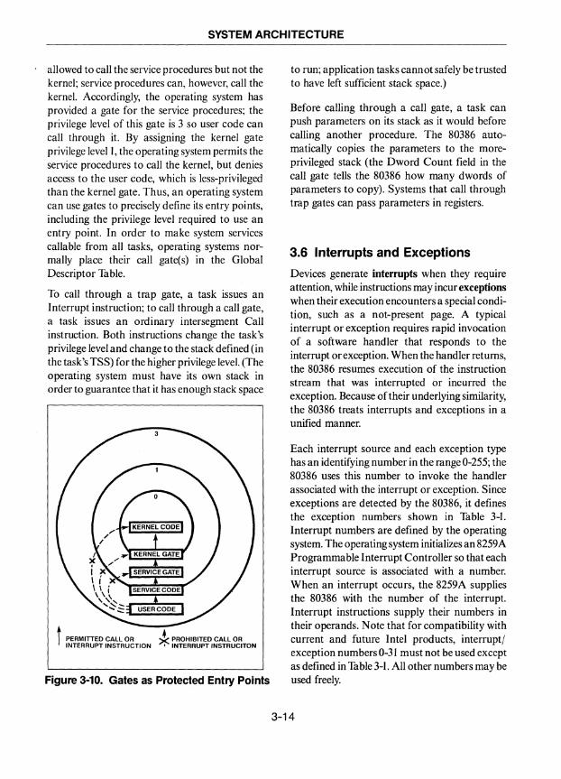
SYSTEM ARCHITECTURE
allowed to call the service procedures but not the kernel; service procedures can, however, call the kernel. Accordingly, the operating system has provided a gate for the service procedures; the privilege level of this gate is 3 so user code can call through it. By assigning the kernel gate privilege level I , the operating system permits the service procedures to call the kernel, but denies access to the user code, which is less-privileged than the kernel gate. Thus, an operating system can use gates to precisely define its entry points, including the privilege level required to use an entry point. In order to make system services callable from all tasks, operating systems normally place their call gate(s) in the Global Descriptor Table.
To call through a trap gate, a task issues an Interrupt instruction; to call through a call gate, a task issues an ordinary intersegment Call instruction. Both instructions change the task's privilege level and change to the stack defined (in the task's TSS) for the higher privilege level. (The operating system must have its own stack in order to guarantee that it has enough stack space
t PERMITIEO CALL DR ~ PROHIBITED CALL DR INTERRUPT INSTRUCTION 0 INTERRUPT INSTRUCITDN
Figure 3-10. Gates as Protected Entry Points
to run; application tasks cannot safely be trusted to have left sufficient stack space.)
Before calling through a call gate, a task can push parameters on its stack as it would before calling another procedure. The 80386 automatically copies the parameters to the moreprivileged stack (the Dword Count field in the call gate tells the 80386 how many dwords of parameters to copy). Systems that call through trap gates can pass parameters in registers.
3.6 Interrupts and Exceptions
Devices generate interrupts when they require attention, while instructions may incur exceptions when their execution encounters a special condition, such as a not-present page. A typical interrupt or exception requires rapid invocation of a software handler that responds to the interrupt or exception. When the handler returns, the 80386 resumes execution of the instruction stream that was interrupted or incurred the exception. Because of their underlying similarity, the 80386 treats interrupts and exceptions in a unified manner.
Each interrupt source and each exception type has an identifying number in the range 0-255; the 80386 uses this number to invoke the handler associated with the interrupt or exception. Since exceptions are detected by the 80386, it defines the exception numbers shown in Table 3-1. Interrupt numbers are defined by the operating system. The operating system initializes an 8259A Programmable Interrupt Controller so that each interrupt source is associated with a number. When an interrupt occurs, the 8259A supplies the 80386 with the number of the interrupt. Interrupt instructions supply their numbers in their operands. Note that for compatibility with current and future Intel products, interrupti exception numbers 0-31 must not be used except as defined in Table 3-1. All other numbers may be used freely.
3-14
SYSTEM ARCHITECTURE
Thble 3-1., Exceptions
ID Description
0 Divide Error
Debug Exception
3 Software Breakpoint
4 Overflow
5 Array Bound Check
6 Invalid Opcode
7 Coprocessor Not Present
8 Double Fault
10 Invalid TSS
11 Segment Fault
12 Stack Under/ Overflow
13 General Protection Violation
14 Page Fault
16 Coprocessor Error
3.6.1. Interrupt Descriptor Table
Having generated or obtained an interrupt or exception number, the 80386 uses the number as an index into the Interrupt Descriptor Table, or IDT. The IDT may be located anywhere in memory; the operating system initializes the IDT and loads its address into the processor's Interrupt Descriptor Table Register (IDTR). Like the GDT or an LDT, the IDT is a vector of descriptors, although gates are the only type of descriptors allowed in the IDT. There is one gate in the IDT for each interrupt and exception handler. (The IDT is functionally similar to the "interrupt vector table" provided by a number of architectures.)
An 80386 interrupt or exception handler can be implemented as a procedure or a task; the merits of these two alternatives are discussed shortly. The 80386 invokes a procedure-based handler much as it performs a gated system
call. To invoke a task-based handler, the 80386 performs a task switch. A handler's IDT gate type tells the processor how to invoke the handler (see Table 3-2). As mentioned, interrupt and trap gates are functionally similar to call gates, except that they have no provision for copying parameters, and they also cause the 80386 to save the Flags register on the handler's stack. They differ from one another only in the state of the Interrupt Enable Flag (IF) at entry to the handler; an interrupt handler is entered with interrupts disabled, while a trap handler, which is typically used to handle exceptions, is entered with interrupts unchanged. As part of switching to a task-based handler, the 80386 loads the Flags register with the value saved in the task's TSS, allowing the handler to run with interrupts enabled or disabled.
Table 3-2. Interrupt and Exception Gate Characteristics
Gate Type Handler Interrupts
Interrupt Procedure Disabled
Trap Procedure Enabled
Task Task (Handler's IF Flag)
Procedure-based handlers are appropriate for routines that should run in the context (that is, use the address space and register values) of the task that is interrupted or incurs the exception. At 16 MHz, the invocation sequence takes 3.6 microseconds. Like any other procedure, an interrupt or exception procedure has access to all of the running task's resources-its data and code, its registers, and its stack. This is as it should be for most exceptions, because a task causes an exception and ready access to task data may be required to resolve it. For example, a page fault handler needs the running task's page tables to find the not-present page's disk address.
3-15
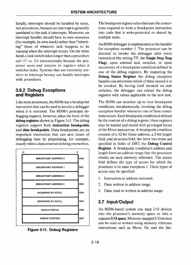
SYSTEM ARCHITECTURE
Ideally, interrupts should be handled by tasks, not procedures, because an interrupt is generally unrelated to the task it interrupts. Moreover, an interrupt handler should have its own resources (for example, its own stack) rather than "inheriting" those of whatever task happens to be running when the interrupt occurs. On the other hand, a task switch takes longer than a procedure call (17 VS. 3.6 microseconds) because the processor saves and restores its registers when it switches tasks. Systems that are extremely sensitive to interrupt latency can handle interrupts with procedures.
3.6.2 Debug E){ceptions and Registers
Like most processors, the 80386 has a breakpoint instruction that can be used to invoke a debugger when it is executed. The 80386's principal debugging support, however, takes the form of the debug registers shown in Figure 3-11. The debug registers support both instruction breakpoints and data breakpoints. Data breakpoints are an important innovation that can save hours of debugging time by pinpointing, for example, exactly when a data structure is being overwritten.
31 o
BREAKPOINT ADDRESS 0 ORO
BREAKPOINT ADDRESS 1 DR1
BREAKPOINT ADDRESS 2 DR2
BREAKPOINT ADDRESS 3 DR3
(RESERVED BY INTEL) DR4
(RESERVED BY INTEL) DR5
DEBUG STATUS DR6
DEBUG CONTROL DR7
Figure 3-11. Debug Registers
The breakpoint registers also eliminate the contortions required to write a breakpoint instruction into code that is write-protected or shared by multiple tasks.
An 80386 debugger is implemented as the handler for exception number 1. The processor can be directed to invoke the debugger after every instruction (by setting TF, the Single Step Trap Flag), upon selected task switches, or upon occurrence of a breakpoint condition defined in one of the debug registers. By inspecting the Debug Status Register the debug exception handler can determine which of these caused it to be invoked. By having itself invoked on task switches, the debugger can reload the debug registers with values applicable to the new task.
The 80386 can monitor up to four breakpoint conditions simultaneously, invoking the debug exception handler whenever one of these conditions occurs. Each breakpoint condition is defined by the content of a debug register; these registers may be loaded and stored with privileged forms ofthe Move instruction. A breakpoint condition consists of a 32-bit linear address, a 2-bit length field, and an access field; the latter two items are specified in fields of DR7, the Debug Control Register. A breakpoint condition's address and length form an address range that the processor checks on each memory reference. The access field defines the type of access for which the processor is to raise exception 1. Three types of access may be specified:
1. Instruction at address executed.
2. Data written in address range.
3. Data read or written in address range.
3.7 InpuVOutput
An 80386-based system can map I/O devices into the processor's memory space or into a separate I/O space. Memory-mapped I/O devices can be read or written using memory reference instructions such as Move, Or, and the like.
3-16
SYSTEM ARCHITECTURE
Memory-mapped devices can be protected by the standard 80386 segment and page protection mechanisms.
In addition to its memory address space, the 80386 has a 64 kilobyte I/O address space. Devices mapped into this space are manipulated with the Input, Output, Input String, and Output String instructions. The first two instructions transfer a byte, word, or dword to or from the EAX register. The latter two instructions transfer a string of bytes, words, or dwords to or from memory.
The 80386 I/O instructions are privilege level sensitive. In the Flags register is a field called I/O Privilege Level (lOPL), which defines the minimum privilege level at which the running task can execute I/O instructions. (IOPL is loaded from the TSS so tasks can have different IOPLs). For example, if a task's 10PL is I, then the task cannot issue I/O instructions except
when it is running at privilege level I or O. The . 10PL mechanism supports multilevel protected operating systems in which, for example, critical and stable kernel procedures run at privilege level 0, and more volatile I/O procedures run at privilege level I; in this case the operating system has only to set IOPL to I when it creates a task. Because IOPL is task-specific, trusted tasks can be allowed execute I/O instructions while running application code, allowing them, for example, to directly manipulate special devices, for which no operating system driver is available.
3-17
To perform direct memory access (DMA) I/O, an 80386 operating system passes a physical address to the DMA controller and must guarantee that the target segment(s) and/ or page(s) do not move during the transfer. One way to mark pages "locked for I/O" is to use one of the three user-defined page table bits.

Chapter 4 4 Architectural Compatibility


CHAPTER 4 ARCHITECTURAL COMPATIBILITY
The 80386 is compatible at the object code level with both the 80286 and the 8086. While it is possible to use the 80386 simply as a fast 80286 or a very fast 8086, its compatibility facilities are substantially more versatile. The 80386 can execute 80286 and 80386 programs concurrently, and, using the 80386's Virtual 86 Mode, existing 8086 programs can also be run concurrently. With the 80386, then, it is possible to build systems that can concurrently execute software written for three generations of Intel 86 family microprocessors.
4.1 80286 Compatibility
The 80286 architecture is a proper subset of the 80386 architecture. Because the 80386 recognizes all 80286 instructions, registers, descriptors, and so on, an 80286 operating system and application programs can be ported to comparable 80386-based hardware without changing a bit.
Direct porting, as described above, is the quickest way to get existing 80286 software running on an 80386-based system. Alternatively, an 80386 operating system can be designed to support existing 80286 applications, while at the same time allowing new applications to use the full facilities of the 80386 architecture (for example, 32-bit parameters and large segments). In such a hybrid design, new applications call the operating system directly, passing 32-bit parameters. The calls of old applications, which are in the 80286's 16-bit format, are intercepted and converted to 32-bit format and then passed to the operating system.
4.2 Real and Virtual 86 Modes
The 80386 can execute 8086 object code in either of two modes, Real Mode or Virtual 86 Mode. The 80386 enters Real Mode when it is reset. In Real Mode, the processor provides fast execution in an unprotected environment like that of an
4-1
8086. Most operating systems will switch from Real Mode to Protected Mode after initialization, but it is also possible to run 8086 software in Real Mode. The principal difference between 80386 Real Mode and an actual 8086 is speed: 8086 programs that are speed-dependent (for example, those that use timing loops) may need minor modifications to run properly on the much faster Real Mode 80386. The great majority of 8086 programs, however, will run without difficulty, just as they do on a Real Mode 80286.
Virtual 86 Mode establishes an 8086 execution environment within the protected multi task environment of the 80386. Where Real Mode governs everything the processor does, Virtual 86 Mode can be applied to selected 80386 tasks. When executing a Virtual 86 Mode task, the processor behaves like an 8086, but upon a switch to a normal task, the processor operates as an 80386 (which, of course, can interpret both 80286 and 80386 programs). Thus, Virtual 86 Mode enables an operating system to support the execution of 8086, 80286, and 80386 programs concurrently.
Chapter 3 described how a task's Task State Segment represents the state of its virtual processor. The VM86 flag in the Flags register, which is loaded from the TSS, defines the running task's virtual processor as an 8086 or an 80386. When the 80386 loads its registers from a TSS whose VM86 flag is set, the processor enters Virtual 86 Mode. When, on a subsequent task switch, the processor loads register values from a TSS whose VM86 flag is clear, it leaves Virtual 86 Mode. Thus, on a task by task basis, the processor emulates an 80386 or an 8086 according to the value of the VM86 flag. The 80386 also leaves Virtual 86 Mode when it raises an exception or is interrupted, making the full resources of the architecture available to interrupt and exception handlers. On return from a handler invoked in Virtual 86 Mode, the 80386 automatically re-enters Virtual 86 Mode.
ARCHITECTURAL COMPATIBILITY
Because the address space of an 8086 is one megabyte, the logical addresses generated by a Virtual 86 Mode task fall into the first megabyte of the 80386 linear address space. Multiple Virtual 86 Mode tasks could interfere with each other, since they would all share the low megabyte of the linear address space. An operating system can use 80386 paging to relocate the linear address spaces of Virtual 86 Mode tasks to different areas of the physical address space. Using paging in this way not only prevents interference among Virtual 86 Mode tasks, but enables a virtual memory operating system to swap the pages of Virtual 86 Mode tasks just as if they were 80386 tasks.
A Virtual 86 Mode task may execute a program that was written for execution on a single-task personal computer. Such a program can contain instructions that are potentially disruptive if executed in a multitasking environment. For example, allowing a Virtual 86 Mode task to execute .the Clear Interrupt Flag instruction, thereby disabling interrupts, could bring the entire system to a halt. To prevent such disruptions, the 80386 raises an exception when a Virtual 86 Mode task attempts to execute an I/O or interrupt-related instruction.
Preventing the execution of such instructions protects the rest of the system from a Virtual 86 Mode task, but does not satisfy the Virtual 86 Mode task's need to execute the instructions. The solution is to simulate the sensitive instructions in an operating system procedure called a virtual machine monitor. When an exception handler is invoked, it can inspect the VM86 flag in the Flags image on the stack to see if the source of the exception is a Virtual 86 Mode task; if so, the exception handler can call the virtual machine monitor which can simulate the instruction and return to the Virtual 86 Mode task. Note that a virtual machine monitor simulates only a few 8086 instructions and that both the simulated instructions and those the 80386 executes directly benefit from the much higher performance of the
4-2
80386 compared to the 8086.
Working together, the 80386 and a virtual machine monitor implement the full 8086 instruction set, and paging can provide each Virtual 86 M ode task with its own protected address space. However, most 8086 programs need additional resources provided by an operating system and peripheral hardware. An example ofthe former type of resource is a file system; an example of the latter is a bit-mapped display controller manipulated directly by an application program. These resources may not exist in the same form in the 80386-based system as they did in the system for which the 8086 program was designed. To simplify the job of providing these resources in a different environment, the 80386 can trap operating system and peripheral references made by Virtual 86 Mode tasks.
For example, most 8086 operating systems use the Interrupt instruction to implement operating system calls. The 80386 raises an exception when a Virtual 86 Mode task attempts to execute an Interrupt instruction. The virtual machine monitor can then translate the 8086 operating system call into a call on the 80386 operating system as shown in Figure 4-I.-If a Virtual 86 Mode task's 10PL is set to less than 3, the 80386 will likewise trap any I/O instruction the 8086 program executes. The 80386 paging facility can be used to redirect references to memory-mapped peripherals to other addresses, if necessary. Such references can also be trapped by marking the corresponding pages read-only (to trap writes), or not-present (to trap both reads and writes).

ARCHITECTURAL COMPATIBILITY
(:::\ V
Figure 4-1. Trapping Virtual 861\11ode System Calls
4-3


Chapter 5 5 Hardware Implementation


CHAPTER 5 HARDWARE IMPLEMENTATION
The 80386 architecture described in the previous chapters is implemented in over 275,000 transistors using Intel's CHMOS III process. This chapter looks briefly inside the 80386 chip, and in more detail at the signals by which the 80386 and other components communicate.
5.1 Internal Design
Figure 5-1 is an abstract view of the functional units that make up the 80386. These six units are arranged in a pipeline that enables them to operate in parallel on different instructions or on different parts of the same instruction. The bus unit performs bus transactions for the other units. When no other unit needs the bus, the prefetch unit reads the next dword of the instruction stream from memory into the prefetch
-
EXECUTION UNIT
REGISTERS
BARREL SHIFTER
MULTIPLY! DIVIDE
ALU
t
SEGMENT UNIT
SEGMENT REGISTERS
SEGMENT
r-- TRANSLATOR
t I
DECODER -INSTRUCTION
QUEUE
queue. In this way, most code fetches are performed in parallel with execution using unneeded bus cycles. The decode unit "cracks" each opcode, converting it into a pointer to the microcode that implements the instruction. The execution unit executes the microinstructions. The execution unit can add two 32-bit registers in 2 clocks. Multiply/ divide hardware performs 32-bit multiplications in 9-41 clocks, depending on the number of significant digits, and 32-bit division in 38 or42 clocks, depending on whether the operands are unsigned or signed. Shift, Rotate, and bit field instructions are aided by a barrel shifter that can shift up to 64 bits in a single clock. In typical instruction mixes that include jumps and calls, the 80386 executes instructions at an average speed of 4.4 clocks each.
PAGE UNIT
TRANSLATION LOOKASIDE
BUFFER
PAGE BUS UNIT
r- TRANSLATOR
t BUS INTERFACE
•
PREFETCH QUEUE
PREFETCHER
DECODE UNIT PREFETCH UNIT
Figure 5-1. Functional Units
5-1

HARDWARE IMPLEMENTATION
Pipelining instruction fetch, decode, and execution units on a single chip is not unusual in modern microprocessors. On the other hand, placing the memory management unit (MMU) in the on-chip pipeline is quite unusual. Incorporating the MMU on the processor chip improves the speed of addresss translation by reducing signal propagation delays (most offchip MMUs introduce at least one wait state), and exploiting the half-clock boundaries that are accessible within the chip (the 80386 clock input is twice the frequency of the chip). The 80386
80287 OR
80387 NUMERIC
COPROCESSOR
82384 CLOCK
GENERATOR
80386 CPU
INTR
MMU consists of the segment and page units shown in Figure 5-1.
The segment unit translates logical addresses to linear addresses, and checks each access for consistency with segment protection attributes. For the majority of instructions, the segment unit obtains the translation and protection data from the 80386's on-chip segment and descriptor registers. The page unit is enabled or disabled by operating system software. When disabled, the linear addresses produced by the segment unit
OPTIONAL
CACHE CONTROL
DRAM CONTROL
MULTIBUS 1/11 INTERFACE
82258 ADVANCED
DMA
DRAM
K:====:> MULTIBUS® 1/11
LOCAL BUS
CONTROL
EPROM
Figure 5-2. Representative System Block Diagram
5-2
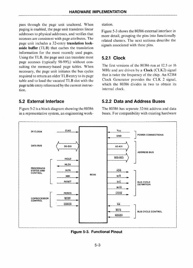
HARDWARE IMPLEMENTATION
pass through the page unit unaltered. When paging is enabled, the page unit translates linear addresses to physical addresses, and verifies that accesses are consistent with page attributes. The page unit includes a 32-entry translation lookaside buffer (TLB) that caches the translation information for the most recently used pages. Using the TLB, the page unit can translate most page accesses (typically 98-99%) without consulting the memory-based page tables. When necessary, the page unit initiates the bus cycles required to return an older TLB entry to its page table and to load the vacated TLB slot with the page table entry referenced by the current instruction.
5.2 External Interface
Figure 5-2 is a block diagram showing the 80386 in a representative system, an engineering work-
2X CLOCK
DATA BUS
PROCESSOR STATUS AND CONTROL [ COPROCESSOB [ CONTROL
A
~
CLK2 •
l\, 00-031
v' HOLD • HLDA
INTR .. NMI .. 80386
RESET •
PEREa • BUSY ..
ERROR ..
station.
Figure 5-3 shows the 80386 external interface in more detail, grouping the pins into functionally related clusters. The next sections describe the signals associated with these pins.
5.2.1 Clock
The first versions of the 80386 run at 12.5 or 16 MHz and are driven by a Clock (CLK2) signal that is twice the frequency of the chip. An 82384 Clock Generator provides the CLK 2 signal, which the 80386 divides in two to obtain its internal clock.
5.2.2 Data and Address Buses
The 80386 has separate 32-bit address and data buses. For compatibility with existing hardware
4 Vee
GND
A2-A31
BEO-BE3
ADS
W/R
DIG
Milo
LOCK
-NA
4
BS16 .. READY
4
~
~
V
] POWER CONNECTIONS
BUS CYCLE DEFINITION
Figure 5-3. Functional Pinout
5-3
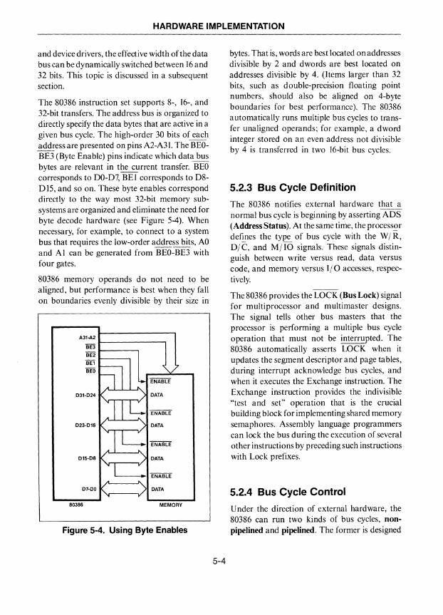
HARDWARE IMPLEMENTATION
and device drivers, the effective width of the data bus can be dynamically switched between 16 and 32 bits. This topic is discussed in a subsequent section.
The 80386 instruction set supports 8-, 16-, and 32-bit transfers. The address bus is organized to directly specify the data bytes that are active in a given bus cycle. The high-order 30 bits of each address are presented on pins A2-A31. The BEOBE3 (Byte Enable) pins indicate which data bus bytes are relevant in the current transfer. BEO corresponds to DO-D7, BEl corresponds to D8-DIS, and so on. These byte enables correspond directly to the way most 32-bit memory subsystems are organized and eliminate the need for byte decode hardware (see Figure 5-4). When necessary, for example, to connect to a system bus that requires the low-order address bits, AO and AI can be generated from BEO-BE3 with four gates.
80386 memory operands do not need to be aligned, but performance is best when they fall on boundaries evenly divisible by their size in
A31-A2 BE3 t----------. BE2 BEl t-------. BED
031-024
023-016
015-08
07-00
80386 MEMORY
Figure 5-4. Using Byte Enables
5-4
bytes. That is, words are best located on addresses divisible by 2 and dwords are best located on addresses divisible by 4. (Items larger than 32 bits, such as double-precision floating point numbers, should also be aligned on 4-byte boundaries for best performance). The 80386 automatically runs mUltiple bus cycles to transfer unaligned operands; for example, a dword integer stored on an even address not divisible by 4 is transferred in two 16-bit bus cycles.
5.2.3 Bus Cycle Definition
The 80386 notifies external hardware that a normal bus cycle is beginning by asserting ADS (Address Status). At the same time, the process~r defines the type of bus cycle with the WI R, DI C, and MI 10 signals. These signals distinguish between write versus read, data versus code, and memory versus 110 accesses, respectively.
The 80386 provides the LOCK (Bus Lock) signal for multiprocessor and multimaster designs. The signal tells other bus masters that the processor is performing a multiple bus cycle operation that must not be interrupted. The 80386 automatically asserts LOCK when it updates the segment descriptor and page tables, during interrupt acknowledge bus cycles, and when it executes the Exchange instruction. The Exchange instruction provides the indivisible "test and set" operation that is the crucial building block for implementing shared memory semaphores. Assembly language programmers can lock the bus during the execution of several other instructions by preceding such instructions with Lock prefixes.
5.2.4 Bus Cycle Control
Under the direction of external hardware, the 80386 can run two kinds of bus cycles, 000-
pipelioed and pipelioed. The former is designed

HARDWARE IMPLEMENTATION
to provide two-clock access to high-speed cache and local memories of any size. (The effectiveness of a memory cache depends on its size relative to the reference patterns of the application.) The latter gives lower-speed memory systems more time to respond to a bus cycle while still keeping the 80386 running at maximum speed. External hardware can dynamically enable pipelining by asserting the N A (N ext Address) pin as described below. By presenting a dynamically selectable choice of bus cycle timings, the 80386 allows hardware engineers to use the mix of memory components that meets price, space, and per-
CLK2 [ (INPUT)
ADDRESS AND [ DEFINITION (OUTPUTS)
ADS [ (OUTPUT)
NA [ (INPUT)
READY [ (INPUT)
DIl-D3l [ (INPUT
FOR READ)
CYCLE 1 (READ)
formance goals, and to adapt a design to exploit advances in memory technology.
Figure 5-5 shows the timing of a non-pipelined bus cycle. The 80386 outputs the bus cycle definition as described above and external hardware signals that it has responded to the bus cycle by asserting READY. If, as often is the case, another bus request is pending in the 80386 when READY is asserted, the processor outputs the next bus cycle definition. With pipelining disabled, the minimum time between address and data is two clocks. External hardware that
CYCLE 2 (READ)
CYCLE 3 (READ)
Figure 5-5. Non-pipelined Bus Cycle Timing
5-5
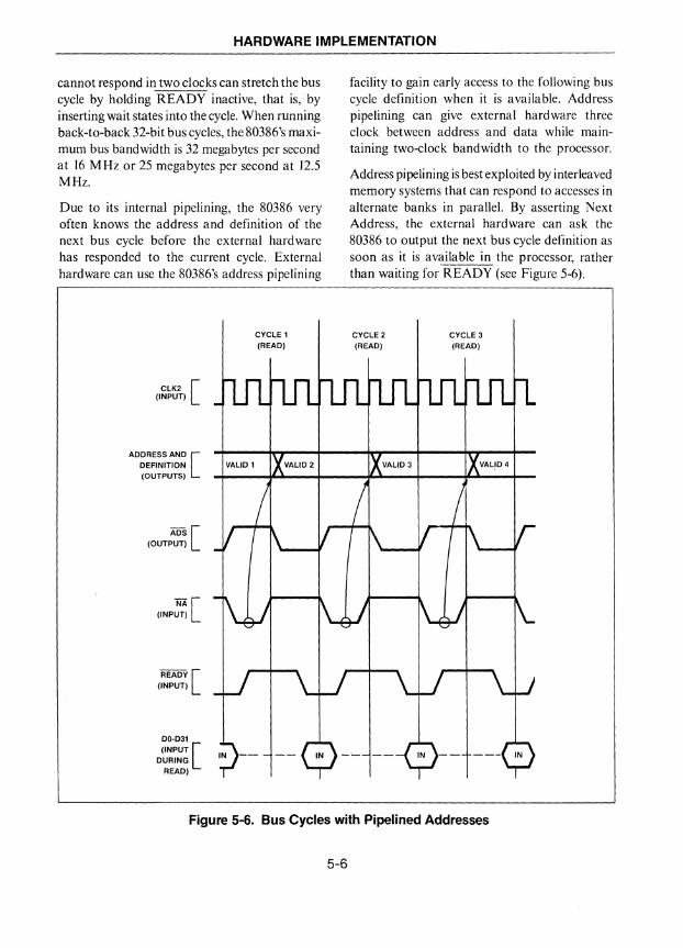
HARDWARE IMPLEMENTATION
cannot respond in two clocks can stretch the bus cycle by holding READY inactive, that is, by inserting wait states into the cycle. When running back-to-back 32-bit bus cycles, the 80386's maximum bus bandwidth is 32 megabytes per second at 16 MHz or 25 megabytes per second at 12.5 MHz.
Due to its internal pipelining, the 80386 very often knows the address and definition of the next bus cycle before the external hardware has responded to the current cycle. External hardware can use the 80386's address pipelining
CLK2 [ (INPUT)
ADDRESS AND [ DEFINITION (OUTPUTS)
ADS [ (OUTPUT)
NA[ (INPUT)
READY [ (INPUT)
00-031
(INPUT [ DURING
READ)
CYCLE 1 (READ)
facility to gain early access to the following bus cycle definition when it is available. Address pipelining can give external hardware three clock between address and data while maintaining two-clock bandwidth to the processor.
Address pipelining is best exploited by interleaved memory systems that can respond to accesses in alternate banks in parallel. By asserting Next Address, the external hardware can ask the 80386 to output the next bus cycle definition as soon as it is available in the processor, rather than waiting for READY (see Figure 5-6).
CYCLE 2 (READ)
CYCLE 3 (READ)
Figure 5-6. Bus Cycles with Pipelined Addresses
5-6
HARDWARE IMPLEMENTATION
5.2.5 Dynamic Bus Sizing
In addition to controlling the timing of bus cycle definitions, the memory (and 1/0) subsystem can also dynamically control the effective size of the data bus. Dynamic bus sizing permits:
I. Arbitrary combinations of 16- and 32-bit memory subsystems; software can make 32-bit transfers without regard to whether it is accessing 16- or 32-bit memory.
2. Simple connection to 16-bit buses, such as the MULTIBUS I bus.
3. Compatibility with 16-bit peripherals (and their drivers) whose registers are usually located on 16- rather than 32-bit boundaries.
By asserting the Bus Size 16 (BSI6) signal, external hardware can instruct the processor to perform the current transfer on only the low 16 bits of the data bus. If BS 16 is asserted, and the access is 32 bits, the processor automatically runs two bus cycles (see Figure 5-7). The 80386 samples BS16 late in the bus cycle, permitting external hardware to assert it only for relevant memory and 110 addresses.
5.2.6 Processor Status and Control
Another bus master (a processor or an intelligent peripheral, such as a DMA controller), can request to use the 80386 local bus by asserting the 80386's HOLD signal. The processor grants the bus by asserting HLDA (Hold Acknowledge) at the end of the current bus cycle (if any); it will then suspend its next bus cycle until HOLD is deasserted. When the 80386 relinquishes the bus to another master, it drives HLDA active and three-states all other pins, electrically isolating itself from the system.
80386 interrupts are classified as maskable or non-maskable; the former arrive on the processor's INTR (Interrupt Request) pin and the latter on its NMI (Non-maskabIe Interrupt
5-7
Request) pin. Operating system software can make the 80386 ignore the INTR pin by clearing the Interrupt Enable flag. The processor always samples the NMI pin; many systems use this pin to inform the processor of an impending power failure or a major system error.
Maskable interrupt requests are usually connected to INTR through one or more 8259A Programmable Interrupt Controllers (PICs). Each 8259A can handle up to eight interrupt sources; multiple 8259As can be cascaded to provide up to 64 different interrupt sources. The operating system initializes each 8259A with an identifying number (vector) to supply for each interrupt source the PIC monitors. The 8259A supplies this number to the 80386 in response to the processor's interrupt acknowledge bus cycle. The 80386 uses the number to invoke the handler designated to respond to the interrupt.
Asserting RESET places the processor in a predefined initial state (in Real Mode with interrupts disabled), and makes it fetch an instruction from physical address FFFFFFFOH.
5.2.7 Coprocessor Control
The 80386 passes instructions and operands to an 80287 or 80387 Numeric Coprocessor by running 110 bus cycles to reserved addresses above the normal 64 kilobyte 110 space. A numeric coprocessor can be selected by A31 high and MilO low. The 80386 uses different communication protocols for each coprocessor, passing 16-bit quantities to the 80287 and 32-bit quantities to the 80387. The 80386 can tell when it is RESET if an 80387 is present; system initialization software can check for the presence of an 80287.
The coprocessor asserts BUSY while it is executing an instruction. The 80386 does not pass the next numeric instruction to the coprocessor until BUSY is negated. Software can synchronize the 80386 with a coprocessor by issuing the

HARDWARE IMPLEMENTATION
WAIT instruction, which suspends the 80386 until BUSY goes inactive. The coprocessor asserts ERROR when it encounters an exception that should be handled by operating system software; the 80386 in turn invokes the numeric
CLK2 [
BEO, BEl [
ADDRESS AND [ DEFINITION
ADS [
BS16 [
READY [
00-015 [
016-031 [
exception handler by raising exception 7. The PEREQ pin is used to implement the 80386-coprocessor protocol.
32-BIT
BUS SIZE
00-015
~-IGNORED
9-Figure 5-7. Mixed 16- and 32-bit Accesses
5-8

Chapter 6 80386 Data Sheet
6


80386 HIGH PERFORMANCE 32-BIT MICROPROCESSOR
WITH ~NTEGRATED MEMORY MANAGEMENT l!II Flexible 32-Bit Microprocessor
- 8, 16, 32-Bit Data Types - 8 General Purpose 32-Bit Registers
[;'] Very Large Address Space - 4 Gigabyte Physical - 64 Terabyte Virtual - 4 Gigabyte Maximum Segment Size
o Integrated Memory Management Unit - Virtual Memory Support - Optional On-Chip Paging - 4 Levels of Protection - Fully Compatible with 80286
o Object Code Compatible with All 8086 Family Microprocessors
o Virtual 8086 Mode Allows Running of 8086 Software in a Protected and Paged System
III Hardware Debugging Support
III Optimized for System Performance - Pipelined Instruction Execution - On-Chip Address Translation Caches -12.5 and 16 MHz Clock - 32 Megabytes/Sec Bus Bandwidth
o High Speed Numerics Support via 80287 and 80387 Coprocessors
o Complete System Development Support - Software: C, PLlM, Assembler
System Generation Tools - Debuggers: PSCOPE, ICETM-386
o High Speed CHMOS III Technology
o 132 Pin Grid Array Package (See Packaging Specification, Order #231369)
The 80386 is an advanced 32-bit microprocessor designed for applications needing very high performance and optimized for multitasking operating systems. The 32-bit registers and data paths support 32-bit addresses and data types. The processor addresses up to four gigabytes of physical memory and 64 terabytes (2**46) of virtual memory. The integrated memory management and protection architecture includes address translation registers, advanced multitasking hardware and a protection mechanism to support operating systems. In addition, the 80386 allows the simultaneous running of multiple operating systems. Instruction pipelining, on-chip address translation, and high bus bandwidth ensure short average instruction execution times and high system throughput. The 80386 processor is capable of execution at sustained rates of between 3 and 4 million instructions per second. The 80386 offers new testability and debugging features. Testability features include a self-test and direct access to the page translation cache. Four new breakpoint registers provide breakpoint traps on code execution or data accesses, for powerful debugging of even ROM-based systems. Object-code compatibility with all iAPX 86 family members (8086, 8088, 80186, 80188, 80286) means the 80386 offers immediate access to the world's largest microprocessor software base.
INSTRUCTION PREDECOOE
DEDICATED ALU BUS
INSTRUCTION PREFETCH
Figure 1-1.80386 Pipelined 32-Bit Microarchitecture
Unix™ is a Trademark of AT&T Bell Labs. MS-DOS is a Trademark of MicroSoft Corporation.
HOLD.INTR,N~I
ERROR,ElOS'i' RESET.HLDA
t.!/IOg,D/CII. W/RN.LOCK~, ADSN.NAH. BSI6/1.READYII
231630-49
Intel Corporation assumes no responsibility for the use of any circuitry other than circuitry embodied in an Intel product. No other circuit patent licenses are implied. Information contained herein supersedes previously published specifications on these devices from Intel. April 1986 © Intel Corporation, 1986
UPDATE NOTICE
This 80386 databook, version -002, contains updates and improvements to the first version. A revision summary is listed here for your convenience.
The sections that are new or significantly revised are:
2.9.6 Interrupt Priorities
2.9.7
2.9.8
2.11.2
2.12
3.1
4.4.3.3
Fig.4-15a
Fig.4-15b
4.6.4
4.6.6
5.6
5.7
5.8
5.8.1
Table 6-3
7.4
7.5
7.6
Fig. 7-8
Fig. 7-9
Fig. 7-10
8.2.3.4
Instruction Restart
Double Faults
TLB Testing
Debugging Support
Real Mode Introduction
liD Privilege Level and liD Permission Bitmap
386TSS
Sample 110 Permission Bitmap
Protection and 110 Permission Bitmap
Entering and Leaving Virtual 8086 Mode
Self-Test Signature
Component and Revision Identifiers
Coprocessor Interfacing
Software Testing for Coprocessor Presence
80386 PGA Package Thermal Characteristics
DC Specifications
AC Specifications
Designing for ICE-386 Use
ICE-386 Processor Module Clearance Requirements
ICE-386 Optional Interface Module Clearance Requirements
Recommended Orientation of Lever-Actuated Socket for ICE-386 Use
Encoding of Address Mode
2
Revised
Revised
Revised
Revised
Revised
Revised
Revised
Revised
New
Revised
Revised
Revised
Revised
New
New
New
Revised
Revised
Revised
New
New
New
Typo fixes for previous pages 122 and 123.
1. TABLE OF CONTENTS ........................................................ 3-5
2. BASE ARCHITECTURE .. . . . . . . . . . . . . . . . . . . . . . . . . . . . . . . . . . . . . . . . . . . . . . . . . . . . . . 7 2.1 Introduction. . . . . . . . . . . . . . . . . . . . . . . . . . . . . . . . . . . . . . . . . . . . . . . . . . . . . . . . . . . . . 7 2.2 Register Overview ....................................................... 7 2.3 Register Descriptions .................................................... 8
2.3.1 General Purpose Registers. . . . . . . . . . . . . . . . . . . . . . . . . . . . . . . . . . . . . . . . . . . . 8 2.3.2 Instruction Pointer .................... . . . . . . . . . . . . . . . . . . . . . . . . . . . . . . . 8 2.3.3 Flags Register. . . . . . . . . . . . . . . . . . . . . . . . . . . . . . . . . . . . . . . . . . . . . . . . . . . . . . . 8 2.3.4 Segment Registers. . . . . . . . . . . . . . . . . . . . . . . . . . . . . . . . . . . . . . . . . . . . . . . . . .. 10 2.3.5 Segment Descriptor Registers. . . . . . . . . . . . . . . . . . . . . . . . . . . . . . . . . . . . . . . .. 11 2.3.6 Control Registers . . . . . . . . . . . . . . . . . . . . . . . . . . . . . . . . . . . . . . . . . . . . . . . . . . .. 11 2.3.7 System Address Registers................. ......... .............. . ... 12 2.3.8 Debug and Test Registers ............................................ 13 2.3.9 Register Accessibility. . . . . . . . . . . . . . . . . . . . . . . . . . . . . . . . . . . . . . . . . . . . . . . .. 13 2.3.10 Compatibility. . . . . . . . . . . . . . . . . . . . . . . . . . . . . . . . . . . . . . . . . . . . . . . . . . . . . . .. 13
2.4 I nstruction Set. . . . . . . . . . . . . . . . . . . . . . . . . . . . . . . . . . . . . . . . . . . . . . . . . . . . . . . . . .. 14 2.4.1 Instruction Set Overview. . . . . . . . . . . . . . . . . . . . . . . . . . . . . . . . . . . . . . . . . . . . .. 14 2.4.2 80386 Instructions. . . . . . . . . . . . . . . . . . . . . . . . . . . . . . . . . . . . . . . . . . . . . . . . . .. 15
2.5 Addressing Modes . . . . . . . . . . . . . . . . . . . . . . . . . . . . . . . . . . . . . . . . . . . . . . . . . . . . . .. 17 2.5.1 Addressing Modes Overview . . . . . . . . . . . . . . . . . . . . . . . . . . . . . . . . . . . . . . . . .. 17 2.5.2 Register and Immediate Modes. . . . . . . . . . . . . . . . . . . . . . . . . . . . . . . . . . . . . . .. 17 2.5.3 32-Bit Memory Addressing Modes ..................................... 17 2.5.4 Differences between 16- and 32- Bit Addresses. . . . . . . . . . . . . . . . . . . . . . . . .. 18
2.6 Data Types ............................................................. 19 2.7 Memory Organization. . . . . . . . . . . . . . . . . . . . . . . . . . . . . . . . . . . . . . . . . . . . . . . . . . . .. 21
2.7.1 Introduction. . . . . . . . . . . . . . . . . . . . . . . . . . . . . . . . . . . . . . . . . . . . . . . . . . . . . . . .. 21 2.7.2 Address Spaces. . . . . . . . . . . . . . . . . . . . . . . . . . . . . . . . . . . . . . . . . . . . . . . . . . . .. 21 2.7.3 Segment Register Usage. . . . . . . . . . . . . . . . . . . . . . . . . . . . . . . . . . . . . . . . . . . .. 22
2.8 1/0 Space ....... . . . . . . . . . . . . . . . . . . . . . . . . . . . . . . . . . . . . . . . . . . . . . . . . . . . . . .. 22 2.9 Interrupts. . . . . . . . . . . . . . . . . . . . . . . . . . . . . . . . . . . . . . . . . . . . . . . . . . . . . . . . . . . . . .. 23
2.9.1 Interrupts and Exceptions. . . . . . . . . . . . . . . . . . . . . . . . . . . . . . . . . . . . . . . . . . . .. 23 2.9.2 Interrupt Processing. . . . . . . . . . . . . . . . . . . . . . . . . . . . . . . . . . . . . . . . . . . . . . . . .. 23 2.9.3 Maskable Interrupt. . . . . . . . . . . . . . . . . . . . . . . . . . . . . . . . . . . . . . . . . . . . . . . . . .. 23 2.9.4 Non-Maskable Interrupt. . . . . . . . . . . . . . . . . . . . . . . . . . . . . . . . . . . . . . . . . . . . . .. 24 2.9.5 Software Interrupts. . . . . . . . . . . . . . . . . . . . . . . . . . . . . . . . . . . . . . . . . . . . . . . . . .. 24 2.9.6 Interrupt and Exception Priorities. . . . . . . . . . . . . . . . . . . . . . . . . . . . . . . . . . . . . .. 25 2.9.7 Instruction Restart. . . . . . . . . . . . . . . . . . . . . . . . . . . . . . . . . . . . . . . . .. . . . . . . . .. 26 2.9.8 Double Faults ..................... . . . . . . . . . . . . . . . . . . . . . . . . . . . . . . . . .. 26
2.10 Reset and Initialization................. ............ ............... ....... 26 2.11 Testability. . . . . . . . . . . . . . . . . . . . . . . . . . . . . . . . . . . . . . . . . . . . . . . . . . . . . . . . . . . . .. 27
2.11.1 Self-Test ........................................................... 27 2.11.2 TLB Testing. . . . . . . . . . . . . . . . . . . . . . . . . . . . . . . . . . . . . . . . . . . . . . . . . . . . . . . .. 27
2.12 Debugging Support ...................................................... 27 2.12.1 Breakpoint Instruction . . . . . . . . . . . . . . . . . . . . . . . . . . . . . . . . . . . . . . . . . . . . . . .. 28 2.12.2 Single-Step Trap. . . . . . . . . . . . . . . . . . . . . . . . . . . . . . . . . . . . . . . . . . . . . . . . . . . .. 28 2.12.3 Debug Registers ....................................... , . . . . . . . . . . . .. 28
2.12.3.1 Linear Address Breakpoint Registers (DRO-DR3) . . . . . . . . . . . . . . . . . . . .. 28 2.12.3.2 Debug Control Register (DR7) . . . . . . . . . . . . . . . . . . . . . . . . . . . . . . . . . . . .. 28 2.12.3.3 Debug Status Register (DR6).... .................................. 31 2.12.3.4 Use of Resume Flag (RF) in Flag Register. . . . . . . . . . . . . . . . . . . . . . . . . .. 31
3
3. REAL MODE ARCHITECTURE. . . . . . . . . . . . . . . . . . . . . . . . . . . . . . . . . . . . . . . . . . . . . . . .. 31 3.1 Real Mode Introduction. . . . . . . . . . . . . . . . . . . . . . . . . . . . . . . . . . . . . . . . . . . . . . . . . .. 31 3.2 Memory Addressing. . . . . . . . . . . . . . . . . . . . . . . . . . . . . . . . . . . . . . . . . . . . . . . . . . . . .. 32 3.3 Reserved Locations. . . . . . . . . . . . . . . . . . . . . . . . . . . . . . . . . . . . . . . . . . . . . . . . . . . . .. 33 3.4 Interrupts. . . . . . . . . . . . . . . . . . . . . . . . . . . . . . . . . . . . . . . . . . . . . . . . . . . . . . . . . . . . . .. 33 3.5 Shutdown and Halt. . . . . . . . . . . . . . . . . . . . . . . . . . . . . . . . . . . . . . . . . . . . . . . . . . . . . .. 33
4. PROTECTED MODE ARCHITECTURE. . . . . . . . . . . . . . . . . . . . . . . . . . . . . . . . . . . . . . . . .. 33 4.1 Introduction.... ......................................................... 33 4.2 Addressing Mechanism. . . . . . . . . . . . . . . . . . . . . . . . . . . . . . . . . . . . . . . . . . . . . . . . . .. 34 4.3 Segmentation . . . . . . . . . . . . . . . . . . . . . . . . . . . . . . . . . . . . . . . . . . . . . . . . . . . . . . . . . .. 35
4.3.1 Segmentation Introduction. . . . . . . . . . . . . . . . . . . . . . . . . . . . . . . . . . . . . . . . . . .. 35 4.3.2 Terminology. . . . . . . . . . . . . . . . . . . . . . . . . . . . . . . . . . . . . . . . . . . . . . . . . . . . . . . .. 35 4.3.3 Descriptor Tables. . . . . . . . . . . . . . . . . . . . . . . . . . . . . . . . . . . . . . . . . . . . . . . . . . .. 35
4.3.3.1 Descriptor Tables Introduction. . . . . . . . . . . . . . . . . . . . . . . . . . . . . . . . . . . .. 35 4.3.3.2 Global Descriptor Table .......................................... 36 4.3.3.3 Local Descriptor Table ........................................... 36 4.3.3.4 Interrupt Descriptor Table. . . . . . . . . . . . . . . . . . . . . . . . . . . . . . . . . . . . . . . .. 36
4.3.4 Descriptors. . . . . . . . . . . . . . . . . . . . . . . . . . . . . . . . . . . . . . . . . . . . . . . . . . . . . . . .. 36 4.3.4.1 Descriptor Attribute Bits .......................................... 36 4.3.4.2 386 Code, Data Descriptors (S = 1)............................. . .. 37 4.3.4.3 System Descriptor Formats ....................................... 38 4.3.4.4 LDT Descriptors (S = 0, TYPE = 2) ............................... 39 4.3.4.5 TSS Descriptors (S = 0, TYPE = 1, 3, 9, B) . . . . . . . . . . . . . . . . . . . . . . . .. 39 4.3.4.6 Gate Descriptors (S = 0 TYPE = 4-7, C, F) .... . . . . . . . . . . . . . . . . . . .. 39 4.3.4.7 Differences Between 386 and 286 Descriptors. . . . . . . . . . . . . . . . . . . . . .. 40 4.3.4.8 Selector Fields ................. . . . . . . . . . . . . . . . . . . . . . . . . . . . . . . . .. 40 4.3.4.9 Segment Descriptor Cache. . . . . . . . . . . . . . . . . . . . . . . . . . . . . . . . . . . . . . .. 40 4.3.4.10 Segment Descriptor Register Settings. . . . . . . . . . . . . . . . . . . . . . . . . . . . .. 41
4.4 Protection. . . . . . . . . . . . . . . . . . . . . . . . . . . . . . . . . . . . . . . . . . . . . . . . . . . . . . . . . . . . .. 45 4.4.1 Protection Concepts ................................................. 45 4.4.2 Rules of Privilege . . . . . . . . . . . . . . . . . . . . . . . . . . . . . . . . . . . . . . . . . . . . . . . . . . .. 45 4.4.3 Privilege Levels. . . . . . . . . . . . . . . . . . . . . . . . . . . . . . . . . . . . . . . . . . . . . . . . . . . . .. 45
4.4.3.1 Task Privilege................ ................................... 45 4.4.3.2 Selector Privilege (RPL) .......................................... 45 4.4.3.3 I/O Privilege Level and I/O Permission Bitmap. . . . . . . . . . . . . . . . . . . . . .. 45 4.4.3.4 Privilege Validation. . . . . . . . . . . . . . . . . . . . . . . . . . . . . . . . . . . . . . . . . . . . . .. 46 4.4.3.5 Descriptor Access ............................... . . . . . . . . . . . . . . .. 46
4.4.4 Privilege Level Transfers. . . . . . . . . . . . . . . . . . . . . . . . . . . . . . . . . . . . . . . . . . . . .. 46 4.4.5 Call Gates .......................................................... 49 4.4.6 Task Switching. . . . . . . . . . . . . . . . . . . . . . . . . . . . . . . . . . . . . . . . . . . . . . . . . . . . .. 49 4.4.7 Initialization and Transition to Protected Mode. . . . . . . . . . . . . . . . . . . . . . . . . .. 50 4.4.8 Tools for Building Protected Systems. . . . . . . . . . . . . . . . . . . . . . . . . . . . . . . . . .. 51
4.5 Paging. . . . . . . . . . . . . . . . . . . . . . . . . . . . . . . . . . . . . . . . . . . . . . . . . . . . . . . . . . . . . . . .. 51 4.5.1 Paging Concepts.. .... .............................................. 51 4.5.2 Paging Organization. . . . . . . . . . . . . . . . . . . . . . . . . . . . . . . . . . . . . . . . . . . . . . . . .. 52
4.5.2.1 Page Mechanism .. . . . . . . . . . . . . . . . . . . . . . . . . . . . . . . . . . . . . . . . . . . . . .. 52 4.5.2.2 Page Descriptor Base Register . . . . . . . . . . . . . . . . . . . . . . . . . . . . . . . . . . .. 52 4.5.2.3 Page Directory .................................................. 52 4.5.2.4 Page Tables .................................................... 53 4.5.2.5 Page Directory/Table Entries. . . . . . . . . . . . . . . . . . . . . . . . . . . . . . . . . . . . .. 53
4.5.3 Page Level Protection (R/W, U/S Bits) ................................. 53 4.5.4 Translation Lookaside Buffer. . . . . . . . . . . . . . . . . . . . . . . . . . . . . . . . . . . . . . . . .. 54 4.5.5 Paging Operation . . . . . . . . . . . . . . . . . . . . . . . . . . . . . . . . . . . . . . . . . . . . . . . . . . .. 54 4.5.6 Operating System Responsibilities .. . . . . . . . . . . . . . . . . . . . . . . . . . . . . . . . . . .. 55
4

4. PROTECTED MODE ARCHITECTURE (Continued) 4.6 Virtual 8086 Environment . . . . . . . . . . . . . . . . . . . . . . . . . . . . . . . . . . . . . . . . . . . . . . . .. 55 4.6.1 Executing 8086 Programs. . . . . . . . . . . . . . . . . . . . . . . . . . . . . . . . . . . . . . . . . . . .. 55 4.6.2 Virtual 8086 Mode Addressing Mechanism . . . . . . . . . . . . . . . . . . . . . . . . . . . . .. 55 4.6.3 Paging In Virtual Mode. . . . . . . . . . . . . . . . . . . . . . . . . . . . . . . . . . . . . . . . . . . . . . .. 55 4.6.4 Protection and Virtual 8086 Mode to 1/0 Permission Bit Map. . . . . . . . . . . . . .. 56 4.6.5 Interrupt Handling. . . . . . . . . . . . . . . . . . . . . . . . . . . . . . . . . . . . . . . . . . . . . . . . . . .. 57 4.6.6 Entering and Leaving Virtual 8086 Mode . . . . . . . . . . . . . . . . . . . . . . . . . . . . . . .. 57
4.6.6.1 Task Switches tolfrom Virtual 8086 Mode. . . . . . . . . . . . . . . . . . . . . . . . . .. 58 4.6.6.2 Transitions Through Trap and Interrupt Gates, and IRET . . . . . . . . . . . . .. 58
5. FUNCTIONAL DATA. . . . . . . . . . . . . . . . . . . . . . . . . . . . . . . . . . . . . . . . . . . . . . . . . . . . . . . . .. 60 5.1 Introduction. . . . . . . . . . . . . . . . . . . . . . . . . . . . . . . . . . . . . . . . . . . . . . . . . . . . . . . . . . . .. 60 5.2 Signal Description ....................................................... 60
5.2.1 Introduction. . . . . . . . . . . . . . . . . . . . . . . . . . . . . . . . . . . . . . . . . . . . . . . . . . . . . . . .. 60 5.2.2 Clock (CLK2) . . . . . . . . . . . . . . . . . . . . . . . . . . . . . . . . . . . . . . . . . . . . . . . . . . . . . . .. 60 5.2.3 Data Bus (DO through 031). . . . . . . . . . . . . . . . . . . . . . . . . . . . . . . . . .. . . . . . . . .. 61 5.2.4 Address Bus (BEO# through BE3#, A2 through A31) .................... 61 5.2.5 Bus Cycle Definition Signals (W/R#, D/C#, MilO, LOCK#) .............. 62 5.2.6 Bus Control Signals. . . . . . . . . . . . . . . . . . . . . . . . . . . . . . . . . . . . . . . . . . . . . . . . .. 63
5.2.6.1 Introduction. . . . . . . . . . . . . . . . . . . . . . . . . . . . . . . . . . . . . . . . . . . . . . . . . . . .. 63 5.2.6.2 Address Status (ADS #) .......................................... 63 5.2.6.3 Transfer Acknowledge (READY#) ................................. 63 5.2.6.4 Next Address Request (NA #) ..................................... 63 5.2.6.5 Bus Size 16 (BS16#)............................................. 63
5.2.7 Bus Arbitration Signals ............................................... 64 5.2.7.1 Introduction . . . . . . . . . . . . . . . . . . . . . . . . . . . . . . . . . . . . . . . . . . . . . . . . . . . .. 64 5.2.7.2 Bus Hold Request (HOLD) ........................................ 64 5.2.7.3 Bus Hold Acknowledge (HLDA) .................................... 64
5.2.8 Coprocessor Interface Signals. . . . . . . . . . . . . . . . . . . . . . . . . . . . . . . . . . . . . . . .. 64 5.2.8.1 Introduction. . . . . . . . . . . . . . . . . . . . . . . . . . . . . . . . . . . . . . . . . . . . . . . . . . . .. 64 5.2.8.2 Coprocessor Request (PEREa). . . . . . . . . . . . . . . . . . . . . . . . . . . . . . . . . . .. 64 5.2.8.3 Coprocessor Busy (BUSY#) ...................................... 64 5.2.8.4 Coprocessor Error (ERROR#) .................................... 65
5.2.9 Interrupt Signals. . . . . . . . . . . . . . . . . . . . . . . . . . . . . . . . . . . . . . . . . . . . . . . . . . . .. 65 5.2.9.1 Introduction..................................................... 65 5.2.9.2 Maskable Interrupt Request (INTR) ................................ 65 5.2.9.3 Non-Maskable Interrupt Request (NMI) ... . . . . . . . . . . . . . . . . . . . . . . . . .. 65 5.2.9.4 Reset (RESET) . . . . . . . . . . . . . . . . . . . . . . . . . . . . . . . . . . . . . . . . . . . . . . . . .. 65
5.2.10 Signal Summary . . . . . . . . . . . . . . . . . . . . . . . . . . . . . . . . . . . . . . . . . . . . . . . . . . . .. 66 5.3. Bus Transfer Mechanism ................................................. 66
5.3.1 Introduction. . . . . . . . . . . . . . . . . . . . . . . . . . . . . . . . . . . . . . . . . . . . . . . . . . . . . . . .. 66 5.3.2 Memory and 1/0 Spaces. . . . . . . . . . . . . . . . . . . . . . . . . . . . . . . . . . . . . . . . . . . . .. 67 5.3.3 Memory and 1/0 Organization. . . . . . . . . . . . . . . . . . . . . . . . . . . . . . . . . . . . . . . .. 68 5.3.4 Dynamic Data Bus Sizing ............................................. 68 5.3.5 Interfacing with 32- and 16-bit Memories. . . . . . . . . . . . . . . . . . . . . . . . . . . . . . .. 69 5.3.6 Operand Alignment .................................................. 70
5.4 Bus Functional Description. . . . . . . . . . . . . . . . . . . . . . . . . . . . . . . . . . . . . . . . . . . . . . .. 70 5.4.1 Introduction. . . . . . . . . . . . . . . . . . . . . . . . . . . . . . . . . . . . . . . . . . . . . . . . . . . . . . . .. 70 5.4.2 Address Pipelining . . . . . . . . . . . . . . . . . . . . . . . . . . . . . . . . . . . . . . . . . . . . . . . . . .. 73 5.4.3 Read and Write Cycles ............................................... 75
5.4.3.1 Introduction. . . . . . . . . . . . . . . . . . . . . . . . . . . . . . . . . . . . . . . . . . . . . . . . . . . .. 75 5.4.3.2 Non-pipelined Address ........................................... 76 5.4.3.3 Non-pipelined Address with Dynamic Data Bus Sizing. . . . . . . . . . . . . . . .. 78
5

5. FUNCTIONAL DATA (Continued) 5.4.3.4 Pipe lined Address ............................................... 80
5.4.3.5 Initiating and Maintaining Pipelined Address. . . . . . . . . . . . . . . . . . . . . . . .. 82 5.4.3.6 Pipelined Address with Dynamic Data Bus Sizing. . . . . . . . . . . . . . . . . . . .. 84
5.4.4 Interrupt Acknowledge (INTA) Cycles....... ..... ... ...... ..... .. ..... .. 86 5.4.5 Halt Indication Cycle ................................................. 87 5.4.6 Shutdown Indication Cycle. . . . . . . . . . . . . . . . . . . . . . . . . . . . . . . . . . . . . . . . . . .. 88
5.5 Other Functional Descriptions . . . . . . . . . . . . . . . . . . . . . . . . . . . . . . . . . . . . . . . . . . . .. 89 5.5.1 Entering and Exiting Hold Acknowledge. . . . . . . . . . . . . . . . . . . . . . . . . . . . . . . .. 89 5.5.2 Reset during Hold Acknowledge. . . . . . . . . . . . . . . . . . . . . . . . . . . . . . . . . . . . . .. 89 5.5.3 Bus Activity During and Following Reset .... . . . . . . . . . . . . . . . . . . . . . . . . . . .. 89
5.6 Self-test Signature. . . . . . . . . . . . . . . . . . . . . . . . . . . . . . . . . . . . . . . . . . . . . . . . . . . . . .. 91 5.7 Component and Revision Identifiers. . . . . . . . . . . . . . . . . . . . . . . . . . . . . . . . . . . . . . .. 91 5.8 Coprocessor Interface. . . . . . . . . . . . . . . . . . . . . . . . . . . . . . . . . . . . . . . . . . . . . . . . . . .. 93
5.8.1 Software Testing for Coprocessor Presence. . . . . . . . . . . . . . . . . . . . . . . . . . . .. 93
6. MECHANICAL DATA ......................................................... 94 6.1 Introduction... ...... ........................ ........... . . . .. ..... .. ..... 94 6.2 Pin Assignment. . . . . . . . . . . . . . . . . . . . . . . . . . . . . . . . . . . . . . . . . . . . . . . . . . . . . . . . .. 94 6.3 Package Dimensions and Mounting .................. . . . . . . . . . . . . . . . . . . . . .. 97 6.4 Package Thermal Specification . . . . . . . . . . . . . . . . . . . . . . . . . . . . . . . . . . . . . . . . . . .. 98
7. ELECTRICAL DATA .......................................................... 100 7.1 Introduction ............................................................. 100 7.2 Power and Grounding .................................................... 100
7.2.1 Power Connections .................................................. 100' 7.2.2 Power Decoupling Recommendations .................................. 100 7.2.3 Resistor Recommendations ........................................... 100 7.2.4 Other Connection Recommendations .................................. 100
7.3 Maximum Ratings ........................................................ 101 7.4 D.C. Specifications ....................................................... 101 7.5 A.C. Specifications ....................................................... 102
7.5.1 A.C. Spec Definitions ................................................. 102 7.5.2 A.C. Specification Tables ............................................. 103 7.5.3 A.C. Test Loads ..................................................... 105 7.5.4 A.C. Timing Waveforms ............................................... 105
7.6 Designing for ICE-386 Use ................................................ 108
8. INSTRUCTION SET ........................................................... 110 8.1 Instruction Encoding and Clock Count Summary ............................. 110 8.2 Instruction Encoding Details ............................................... 125
8.2.1 Overview ........................................................... 125 8.2.2 32-Bit Extensions of the Instruction Set ................................. 126 8.2.3 Encoding of Instruction Fields ......................................... 126
8.2.3.1 Encoding of the Operand Length (w) Field ........................... 126 8.2.3.2 Encoding of the General Register (reg) Field ........................ 126 8.2.3.3 Encoding of the Segment Register (sreg) Field ....................... 127 8.2.3.4 Encoding of Address Mode ....................................... 127 8.2.3.5 Encoding of Operation Direction (d) Field ........................... 131 8.2.3.6 Encoding of Sign-extend (s) Field .................................. 131 8.2.3.7 Encoding of Conditional Test (tUn) Field ............................ 131 8.2.3.8 Encoding of Control or Debug or Test Register (eee) Field ............. 131
NOTE This is revision 002; This supercedes all previous revisions.
6
80386
2. BASE ARCHITECTURE
2.1 INTRODUCTION
The B03B6 consists of a central processing unit, a memory management unit and a bus interface.
The central processing unit consists of the execution unit and instruction unit. The execution unit contains the eight 32-bit general purpose registers which are used for both address calculation, data operations and a 64-bit barrel shifter used to speed shift, rotate, multiply, and divide operations. The multiply and divide logic uses a 1-bit per cycle algorithm. The multiply algorithm stops the iteration when the most significant bits of the multiplier are all zero. This allows typical 32-bit multiplies to be executed in under one microsecond. The instruction unit decodes the instruction opcodes and stores them in the decoded instruction queue for immediate use by the execution unit.
The memory management unit (MMU) consists of a segmentation unit and a paging unit. Segmentation allows the managing of the logical address space by providing an extra addressing component, one that allows easy code and data relocatability, and efficient sharing. The paging mechanism operates beneath and is transparent to the segmentation process, to allow management of the physical address space. Each segment is divided into one or more 4K byte pages. To implement a virtual memory system, the B03B6 supports full restartability for all page and segment faults.
Memory is organized into one or more variable length segments, each up to four gigabytes in size. A given region of the linear address space, a segment, can have attributes associated with it. These attributes include its location, size, type (Le. stack, code or data), and protection characteristics. Each task on an B03B6 can have a maximum of 16,3B1 segments of up to four gigabytes each, thus providing 64 terabytes (trillion bytes) of virtual memory to each task.
The segmentation unit provides four-levels of protection for isolating and protecting applications and the operating system from each other. The hardware enforced protection allows the design of systems with a high degree of integrity.
The 80386 has two modes of operation: Real Address Mode (Real Mode), and Protected Virtual Address Mode (Protected Mode). In Real Mode the B0386 operates as a very fast 80B6, but with 32-bit extensions if desired. Real Mode is required primari-
7
Iy to setup the processor for Protected Mode operation. Protected Mode provides access to the sophisticated memory management, paging and privilege capabilities of the processor.
Within Protected Mode, software can perform a task switch to enter into tasks designated as Virtual B086 Mode tasks. Each such task behaves with BOB6 semantics, thus allowing BOB6 software (an application program, or an entire operating system) to execute. The Virtual 80B6 tasks can be isolated and protected from one another and the host B0386 operating system, by the use of paging, and the 110 Permission Bitmap.
Finally, to facilitate high performance system hardware designs, the 80386 bus interface offers address pipelining, dynamic data bus sizing, and direct Byte Enable signals for each byte of the data bus. These hardware features are described fully beginning in Section 5.
2.2 REGISTER OVERVIEW
The B0386 has 32 register resources in the following categories:
o General Purpose Registers
o Segment Registers
o Instruction Pointer and Flags
o Control Registers
o System Address Registers
o Debug Registers
o Test Registers.
The registers are a superset of the 8086, 80186 and B0286 registers, so all 16-bit 8086, B0186 and 802B6 registers are contained within the 32-bit 803B6.
Figure 2-1 shows all of B0386 base architecture registers, which include the general address and data registers, the instruction pointer, and the flags register. The contents of these registers are task-specific, so these registers are automatically loaded with a new context upon a task switch operation.
The base architecture also includes six directly accessible segments, each up to 4 Gbytes in size. The segments are indicated by the selector values placed in 80386 segment registers of Figure 2-1. Various selector values can be loaded as a program executes, if desired.
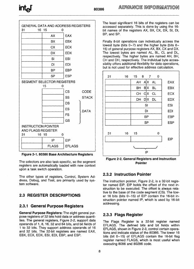
inter 80386
GENERAL DATA AND ADDRESS REGISTERS 31 16 15 0
AX EAX
BX EBX
CX ECX
DX EDX
SI ESI
DI EDI
BP EBP
SP ESP
SEGMENT SELECTOR REGISTERS 15 0
CS CODE
SS STACK
DS
} DATA ES
FS
GS
INSTRUCTION POINTER AND FLAGS REGISTER 31 16 15 0
I I IP I EIP
FLAGS : EFLAGS
Figure 2-1. 80386 Base Architecture Registers
The selectors are also task-specific, so the segment registers are automatically loaded with new context upon a task switch operation.
The other types of registers, Control, System Address, Debug, and Test, are primarily used by system software.
2.3 REGISTER DESCRIPTIONS
2.3.1 General Purpose Registers
General Purpose Registers: The eight general purpose registers of 32 bits hold data or address quantities. The general registers, Figure 2-2, support data operands of 1, 8, 16, 32 and 64 bits, and bit fields of 1 to 32 bits. They support address operands of 16 and 32 bits. The 32-bit registers are named EAX, EBX, ECX, EDX, ESI, EDI, EBP, and ESP.
8
The least significant 16 bits of the registers can be accessed separately. This is done by using the 16-bit names of the registers AX, BX, CX, DX, SI, DI, BP, and SP.
Finally 8-bit operations can individually access the lowest byte (bits 0-7) and the higher byte (bits 8-15) of general purpose registers AX, BX, CX and DX. The lowest bytes are named AL, BL, CL and DL, respectively. The higher bytes are named AH, BH, CH and DH, respectively. The individual byte accessibility offers additional flexibility for data operations, but is not used for effective address calculation.
31 16 15 8 7 0
AH AX AL EAX
BH BX BL EBX
CH CX CL ECX
DH DX DL EDX
SI ESI
DI EDI
BP EBP
SP ESP
31 16 15 0
I I I EIP
\. • }
IP
Figure 2-2. General Registers and Instruction Pointer
2.3.2 Instruction Pointer
The instruction pointer, Figure 2-2, is a 32-bit register named EIP. EIP holds the offset of the next instruction to be executed. The offset is always relative to the base of the code segment (CS). The lower 16 bits (bits 0-15) of EIP contain the 16-bit instruction pointer named IP, which is used by 16-bit addressing.
2.3.3 Flags Register
The Flags Register is a 32-bit register named EFLAGS. The defined bits and bit fields within EFLAGS, shown in Figure 2-3, control certain operations and indicate status of the 80386. The lower 16 bits (bit 0 -15) of EFLAGS contain the 16-bit flag register named FLAGS, which is most useful when executing 8086 and 80286 code.

inter 80386
FLAGS
3 3 2 2 2 2 2 2 2 222 1 1 1 1 1 1 1 1 1 1 0 9 8 7 6 5 432 1 0 9 8 7 6 5 4 3 2 0 9 8 7 6 5 432 1 0
EFLAGS RESERVED FOR INTEL
VIRTUAL MODE---------'
RESUME FLAG -:;:;.:======::::'-.J NESTED TASK FLAG I/O PRIVILEGE LEVEL----------' OVERFLOW--------------'
DIRECTION FLAG"7===========:::::::~ INTERRUPT ENABLE
231630-50
Figure 2-3. Flags Register
VM (Virtual 8086 Mode, bit 17)
The VM bit provides Virtual 8086 Mode within Protected Mode. If set while the 80386 is in Protected Mode, the 80386 will switch to Virtual 8086 operation, handling segment loads as the 8086 does, but generating exception 13 faults on privileged opcodes. The VM bit can be set only in Protected Mode, by the IRET instruction (if current privilege level = 0) and by task switches at any privilege level. The VM bit is unaffected by POPF. PUSHF always pushes a a in this bit, even if executing in virtual 8086 Mode. The EFLAGS image pushed during interrupt processing or saved during task switches will contain a 1 in this bit if the interrupted code was executing as a Virtual 8086 Task.
RF (Resume Flag, bit 16)
The RF flag is used in conjunction with the debug register breakpoints. It is checked at instruction boundaries before breakpoint processing. When RF is set, it causes any debug fault to be ignored on the next instruction. RF is then automatically reset at the successful completion of every instruction (no faults are signalled) except the IRET instruction, the POPF instruction, (and JMP, CALL, and INT instructions causing a task switch). These instructions set RF to the value specified by the memory image. For example, at the end of the breakpoint service routine,
9
the IRET instruction can pop an EFLAG image having the RF bit set and resume the program's execution at the breakpoint address without generating another breakpoint fault on the same location.
NT (Nested Task, bit 14)
This flag applies to Protected Mode. NT is set to indicate that the execution of this task is nested within another task. If set, it indicates that the current nested task's Task State Segment (TSS) has a valid back link to the previous task's TSS. This bit is set or reset by control transfers to other tasks. The value of NT in EFLAGS is tested by the IRET instruction to determine whether to do an inter-task return or an intra-task return. A POPF or an IRET instruction will affect the setting of this bit according to the image popped, at any privilege level.
10PL (Input/Output Privilege Level, bits 12-13)
This two-bit field applies to Protected Mode. 10PL indicates the numerically maximum CPL (current privilege level) value permitted to execute 1/0 instructions without generating an exception 13 fault or consulting the 1/0 Permission Bitmap. It also indicates the maximum CPL value allowing alteration of the IF (INTR Enable Flag) bit when new values are popped into the EFLAG register. POPF and IRET instruction can alter the 10PL field when executed at CPL = O. Task switches can always alter the 10PL field, when the new flag image is loaded from the incoming task's TSS.
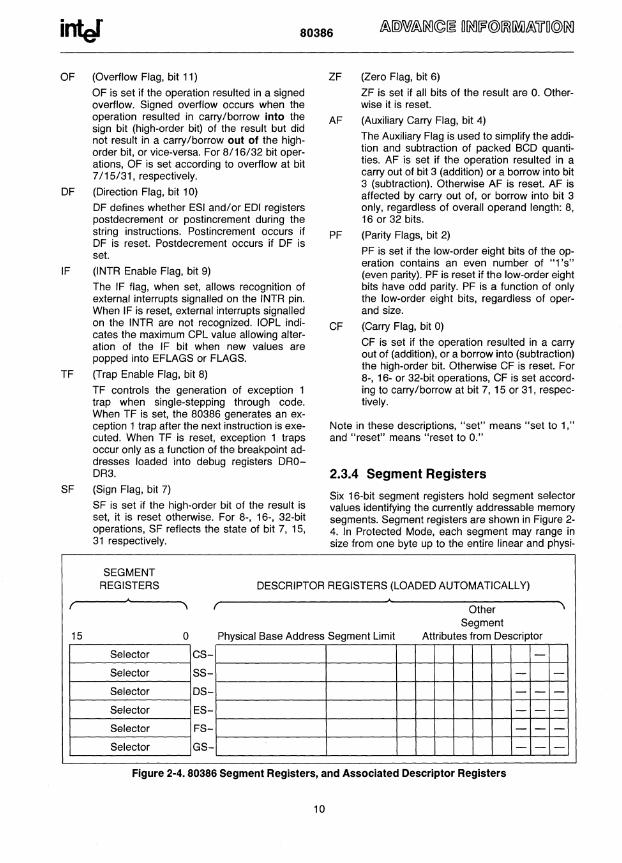
inter 80386
OF (Overflow Flag, bit 11)
OF is set if the operation resulted in a signed overflow. Signed overflow occurs when the operation resulted in carry/borrow into the sign bit (high-order bit) of the result but did not result in a carry/borrow out of the highorder bit, or vice-versa. For 8/16/32 bit operations, OF is set according to overflow at bit 7/15/31, respectively.
DF (Direction Flag, bit 10)
DF defines whether ESI and/or EDI registers postdecrement or postincrement during the string instructions. Postincrement occurs if DF is reset. Postdecrement occurs if DF is set.
IF (INTR Enable Flag, bit 9)
The IF flag, when set, allows recognition of external interrupts signalled on the INTR pin. When IF is reset, external interrupts signalled on the INTR are not recognized. IOPL indicates the maximum CPL value allowing alteration of the IF bit when new values are popped into EFLAGS or FLAGS.
TF (Trap Enable Flag, bit 8)
TF controls the generation of exception 1 trap when single-stepping through code. When TF is set, the 80386 generates an exception 1 trap after the next instruction is executed. When TF is reset, exception 1 traps occur only as a function of the breakpoint addresses loaded into debug registers DRODR3.
SF (Sign Flag, bit 7)
SF is set if the high-order bit of the result is set, it is reset otherwise. For 8-, 16-, 32-bit operations, SF reflects the state of bit 7, 15, 31 respectively.
SEGMENT
ZF (Zero Flag, bit 6)
ZF is set if all bits of the result are O. Otherwise it is reset.
AF (Auxiliary Carry Flag, bit 4)
The Auxiliary Flag is used to simplify the addition and subtraction of packed BCD quantities. AF is set if the operation resulted in a carry out of bit 3 (addition) or a borrow into bit 3 (subtraction). Otherwise AF is reset. AF is affected by carry out of, or borrow into bit 3 only, regardless of overall operand length: 8, 16 or 32 bits.
PF (Parity Flags, bit 2)
PF is set if the low-order eight bits of the operation contains an even number of "1 's" (even parity). PF is reset if the low-order eight bits have odd parity. PF is a function of only the low-order eight bits, regardless of operand size.
CF (Carry Flag, bit 0)
CF is set if the operation resulted in a carry out of (addition), or a borrow into (subtraction) the high-order bit. Otherwise CF is reset. For 8-, 16- or 32-bit operations, CF is set according to carry/borrow at bit 7, 15 or 31, respectively.
Note in these descriptions, "set" means "set to 1," and "reset" means "reset to 0."
2.3.4 Segment Registers
Six 16-bit segment registers hold segment selector values identifying the currently addressable memory segments. Segment registers are shown in Figure 2-4. In Protected Mode, each segment may range in size from one byte up to the entire linear and physi-
REGISTERS DESCRIPTOR REGISTERS (LOADED AUTOMATICALLY) A A
( \ ( Other \
Segment 15 0 Physical Base Address Segment Limit Attributes from Descriptor
Selector CS- -Selector SS- - -Selector DS- - - -Selector ES- - - -Selector FS- - - -Selector GS- - - -
Figure 2-4. 80386 Segment Registers, and Associated Descriptor Registers
10
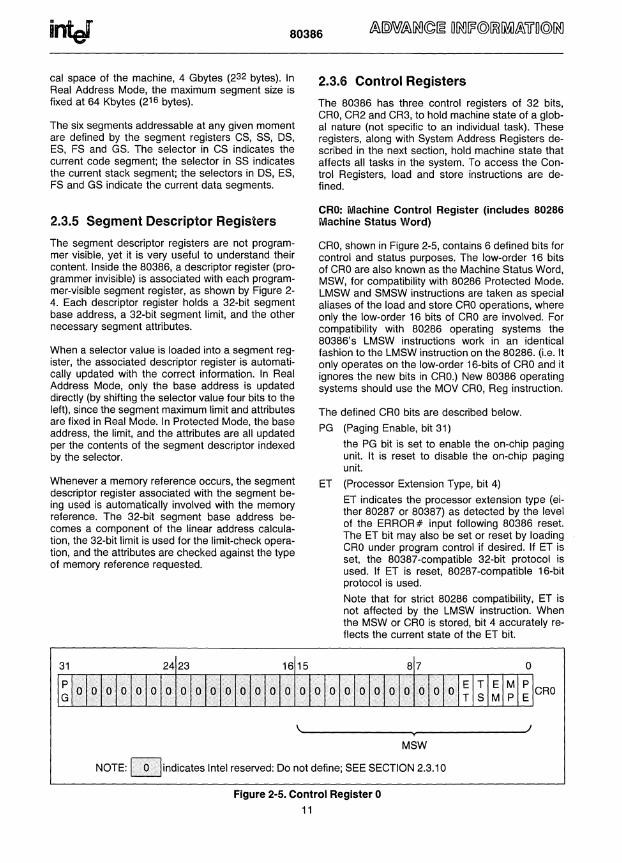
80386
cal space of the machine, 4 Gbytes (232 bytes). In Real Address Mode, the maximum segment size is fixed at 64 Kbytes (216 bytes).
The six segments addressable at any given moment are defined by the segment registers CS, SS, OS, ES, FS and GS. The selector in CS indicates the current code segment; the selector in SS indicates the current stack segment; the selectors in OS, ES, FS and GS indicate the current data segments.
2.3.5 Segment Descriptor Registers
The segment descriptor registers are not programmer visible, yet it is very useful to understand their content. Inside the 80386, a descriptor register (programmer invisible) is associated with each programmer-visible segment register, as shown by Figure 2-4. Each descriptor register holds a 32-bit segment base address, a 32-bit segment limit, and the other necessary segment attributes.
When a selector value is loaded into a segment register, the associated descriptor register is automatically updated with the correct information. In Real Address Mode, only the base address is updated directly (by shifting the selector value four bits to the left), since the segment maximum limit and attributes are fixed in Real Mode. In Protected Mode, the base address, the limit, and the attributes are all updated per the contents of the segment descriptor indexed by the selector.
Whenever a memory reference occurs, the segment descriptor register associated with the segment being used is automatically involved with the memory reference. The 32-bit segment base address becomes a component of the linear address calculation, the 32-bit limit is used for the limit-check operation, and the attributes are checked against the type of memory reference requested.
2.3.6 Control Registers
The 80386 has three control registers of 32 bits, CRO, CR2 and CR3, to hold machine state of a global nature (not specific to an individual task). These registers, along with System Address Registers described in the next section, hold machine state that affects all tasks in the system. To access the Control Registers, load and store instructions are defined.
CRO: Machine Control Register (includes 80286 Machine Status Word)
CRO, shown in Figure 2-5, contains 6 defined bits for control and status purposes. The low-order 16 bits of CRO are also known as the Machine Status Word, MSW, for compatibility with 80286 Protected Mode. LMSW and SMSW instructions are taken as special aliases of the load and store CRO operations, where only the low-order 16 bits of CRO are involved. For compatibility with 80286 operating systems the 80386's LMSW instructions work in an identical fashion to the LMSW instruction on the 80286. (Le. It only operates on the low-order l6-bits of CRO and it ignores the new bits in CRO.) New 80386 operating systems should use the MOV CRO, Reg instruction.
The defined CRO bits are described below.
PG (Paging Enable, bit 31)
the PG bit is set to enable the on-chip paging unit. It is reset to disable the on-chip paging unit.
ET (Processor Extension Type, bit 4)
ET indicates the processor extension type (either 80287 or 80387) as detected by the level of the ERROR# input following 80386 reset. The ET bit may also be set or reset by loading CRO under program control if desired. If ET is set, the 80387-compatible 32-bit protocol is used. If ET is reset, 80287-compatible 16-bit protocol is used.
Note that for strict 80286 compatibility, ET is not affected by the LMSW instruction. When the MSW or CRO is stored, bit 4 accurately reflects the current state of the ET bit.
~~---------------y--------------~} MSW
NOTE: f' :;~~\I indicates I ntel reserved: Do not define; SEE SECTION 2.3.10
Figure 2-5. Control Register 0
11
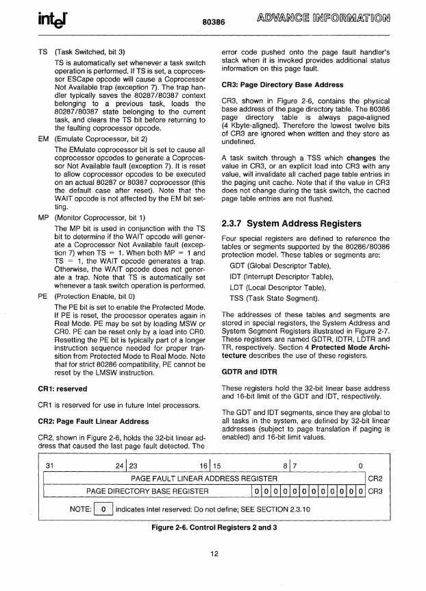
inter 80386
TS (Task Switched, bit 3)
TS is automatically set whenever a task switch operation is performed. If TS is set, a coprocessor ESCape opcode will cause a Coprocessor Not Available trap (exception 7). The trap handier typically saves the 80287/80387 context belonging to a previous task, loads the 80287/80387 state belonging to the current task, and clears the TS bit before returning to the faulting coprocessor opcode.
EM (Emulate Coprocessor, bit 2)
The EMulate coprocessor bit is set to cause all coprocessor opcodes to generate a Coprocessor Not Available fault (exception 7). It is reset to allow coprocessor opcodes to be executed on an actual 80287 or 80387 coprocessor (this the default case after reset). Note that the WAIT opcode is not affected by the EM bit setting.
MP (Monitor Coprocessor, bit 1)
The MP bit is used in conjunction with the TS bit to determine if the WAIT opcode will generate a Coprocessor Not Available fault (exception 7) when TS = 1. When both MP = 1 and TS = 1, the WAIT opcode generates a trap. Otherwise, the WAIT opcode does not generate a trap. Note that TS is automatically set whenever a task switch operation is performed.
PE (Protection Enable, bit 0)
The PE bit is set to enable the Protected Mode. If PE is reset, the processor operates again in Real Mode. PE may be set by loading MSW or CRO. PE can be reset only by a load into CRO. Resetting the PE bit is typically part of a longer instruction sequence needed for proper transition from Protected Mode to Real Mode. Note that for strict 80286 compatibility, PE cannot be reset by the LMSW instruction.
CR1: reserved
CR1 is reserved for use in future Intel processors.
CR2: Page Fault Linear Address
CR2, shown in Figure 2-6, holds the 32-bit linear address that caused the last page fault detected. The
error code pushed onto the page. fault handler's stack when it is invoked provides additional status information on this page fault.
CR3: Page Directory Base Address
CR3, shown in Figure 2-6, contains the physical base address of the page directory table. The 80386 page directory table is always page-aligned (4 Kbyte-aligned). Therefore the lowest twelve bits of CR3 are ignored when written and they store as undefined.
A task switch through a TSS which changes the value in CR3, or an explicit load into CR3 with any value, will invalidate all cached page table entries in the paging unit cache. Note that if the value in CR3 does not change during the task switch, the cached page table entries are not flushed.
2.3.7 System Address Registers
Four special registers are defined to reference the tables or segments supported by the 80286/80386 protection model. These tables or segments are:
GDT (Global Descriptor Table),
IDT (Interrupt Descriptor Table),
LDT (Local Descriptor Table),
TSS (Task State Segment).
The addresses of these tables and segments are stored in special registers, the System Address and System Segment Registers illustrated in Figure 2-7. These registers are named GDTR, IDTR, LDTR and TR, respectively. Section 4 Protected Mode Architecture describes the use of these registers.
GDTR and IDTR
These registers hold the 32-bit linear base address and 16-bit limit of the GDT and IDT, respectively.
The GDT and IDT segments, since they are global to all tasks in the system, are defined by 32-bit linear addresses (subject to page translation if paging is enabled) and 16-bit limit values.
31 24 23 16 15 8 7 o PAGE FAULT LINEAR ADDRESS REGISTER CR2
r--------------------------------------.~~_r_r~~~r_~_._4
PAGE DIRECTORY BASE REGISTER 00 0 CR3
NOTE: I· .0:1 indicates Intel reserved: Do not define; SEE SECTION 2.3.10
Figure 2-6. Control Registers 2 and 3
12
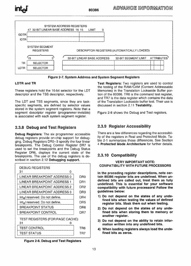
80386
SYSTEM ADDRESS REGISTERS 47 32-BITLINEARBASEADDRESS 1615 LIMIT 0
~~~:I I I SYSTEM SEGMENT
REGISTERS DESCRIPTOR REGISTERS (AUTOMATICALLY LOADED)
~5 ( 32-BIT LINEAR BASE ADDRESS 32-BIT SEGMENT LIMIT ATTRIBUTES\
I " II TR SELECTOR
LDTR SELECTOR
Figure 2-7. System Address and System Segment Registers
LDTR and TR
These registers hold the 16-bit selector for the LOT descriptor and the TSS descriptor, respectively.
The LOT and TSS segments, since they are taskspecific segments, are defined by selector values stored in the system segment registers. Note that a segment descriptor register (programmer-invisible) is associated with each system segment register.
2.3.8 Debug and Test Registers
Debug Registers: The six programmer accessible debug registers provide on-chip support for debugging. Debug Registers DRO-3 specify the four linear breakpoints. The Debug Control Register DR? is used to set the breakpoints and the Debug Status Register DR6, displays the current state of the breakpoints. The use of the debug registers is described in section 2.12 Debugging support.
DEBUG REGISTERS 31 0
LINEAR BREAKPOINT ADDRESS 0 ORO
LINEAR BREAKPOINT ADDRESS 1 DR1
LINEAR BREAKPOINT ADDRESS 2 DR2
LINEAR BREAKPOINT ADDRESS 3 DR3
Intel reserved. Do not define. DR4
Intel reserved. Do not define. DR5
BREAKPOINT STATUS DR6
BREAKPOINT CONTROL DR?
TEST REGISTERS (FOR PAGE CACHE) 31 0
I TEST CONTROL
I TR6
TR? TEST STATUS
Figure 2-8. Debug and Test Registers
13
Test Registers: Two registers are used to control the testing of the RAM/CAM (Content Addressable Memories) in the Translation Lookaside Buffer portion of the 80386. TR6 is the command test register, and TR? is the data register which contains the data of the Translation Lookaside buffer test. Their use is discussed in section 2.11 Testability.
Figure 2-8 shows the Debug and Test registers.
2.3.9 Register Accessibility
There are a few differences regarding the accessibility of the registers in Real and Protected Mode. Table 2-1 summarizes these differences. See Section 4 Protected Mode Architecture for further details.
2.3.10 Compatibility
VERY IMPORTANT NOTE: COMPATIBILITY WITH FUTURE PROCESSORS
In the preceding register descriptions, note certain 80386 register bits are undefined. When undefined bits are called out, treat them as fully undefined. This is essential for your software compatibility with future processorsl Follow the guidelines below: 1) Do not depend on the states of any unde
fined bits when testing the values of defined register bits. Mask them out when testing.
2) Do not depend on the states of any undefined bits when storing them to memory or another register.
3) Do not depend on the ability to retain information written into any undefined bits.
4) When loading registers always load the undefined bits as zeros.
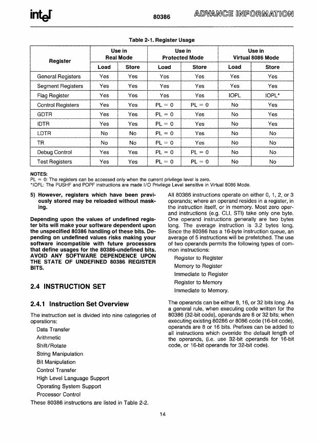
inter 80386
Table 2-1. Register Usage
Use in Use in Use in
Register Real Mode Protected Mode Virtual 8086 Mode
Load Store Load Store Load Store
General Registers Yes Yes Yes Yes Yes Yes
Segment Registers Yes Yes Yes Yes Yes Yes
Flag Register Yes Yes Yes Yes IOPL IOPL'
Control Registers Yes Yes PL = 0 PL = 0 No Yes
GDTR Yes Yes PL = 0 Yes No Yes
IDTR Yes Yes PL = 0 Yes No Yes
LDTR No No PL = 0 Yes No No
TR No No PL = 0 Yes No No
Debug Control Yes Yes PL = 0 PL = 0 No No
Test Registers Yes Yes PL = 0 PL = 0 No No
NOTES: PL = 0: The registers can be accessed only when the current privilege level is zero. 'IOPL: The PUSHF and POPF instructions are made I/O Privilege Level sensitive in Virtual 8086 Mode.
5) However, registers which have been previously stored may be reloaded without masking.
Depending upon the values of undefined register bits will make your software dependent upon the unspecified 80386 handling of these bits. Depending on undefined values risks making your software incompatible with future processors that define usages for the 80386-undefined bits. AVOID ANY SOFTWARE DEPENDENCE UPON THE STATE OF UNDEFINED 80386 REGISTER BITS.
2.4 INSTRUCTION SET
2.4.1 Instruction Set Overview
The instruction set is divided into nine categories of operations:
Data Transfer
Arithmetic
Shift/Rotate
String Manipulation
Bit Manipulation
Control Transfer
High Level Language Support
Operating System Support
Processor Control
These 80386 instructions are listed in Table 2·2.
14
All 80386 instructions operate on either 0, 1, 2, or 3 operands; where an operand resides in a register, in the instruction itself, or in memory. Most zero oper· and instructions (e.g. CLI, STI) take only one byte. One operand instructions generally are two bytes long. The average instruction is 3.2 bytes long. Since the 80386 has a 16·byte instruction queue, an average of 5 instructions will be prefetched. The use of two operands permits the following types of common instructions:
Register to Register
Memory to Register
Immediate to Register
Register to Memory
Immediate to Memory.
The operands can be either 8, 16, or 32 bits long. As a general rule, when executing code written for the 80386 (32-bit code), operands are 8 or 32 bits; when executing existing 80286 or 8086 code (16-bit code), operands are 8 or 16 bits. Prefixes can be added to all instructions which override the default length of the operands, (Le. use 32-bit operands for 16-bit code, or 16-bit operands for 32-bit code).

80386
2.4.2 80386 Instructions Table 2-2b Arithmetic Instructions
Table 2-2a Data Transfer ADDITION
GENERAL PURPOSE ADD Add operands
MOV Move operand ADC Add with carry
PUSH Push operand onto stack INC Increment operand by 1
POP Pop operand off stack AAA ASCII adjust for addition
PUSHA Push all registers on stack DAA Decimal adjust for addition
POPA Pop all registers off stack SUBTRACTION
XCHG Exchange Operand, Register SUB Subtract operands
XLAT Translate SBB Subtract with borrow
CONVERSION DEC Decrement operand by 1
MOVZX Move byte or Word, Dword, with zero NEG Negate operand extension CMP Compare operands
MOVSX Move byte or Word, Dword, sign DAS Decimal adjust for subtraction extended
CBW Convert byte to Word, or Word to Dword AAS ASCII Adjust for subtraction
MULTIPLICATION CWO Convert Word to DWORD
CWDE Convert Word to DWORD extended
COO Convert DWORD to aWORD
MUL Multiply Double/Single Precision
IMUL Integer multiply
AAM ASCII adjust after multiply INPUT !OUTPUT DIVISION
IN Input operand from I/O space
OUT Output operand to I/O space DIV Divide unsigned
IDIV Integer Divide ADDRESS OBJECT AAD ASCII adjust before division
LEA Load effective address
LOS Load pointer into 0 segment register Table 2-2c String Instructions
LES Load pointer into E segment register MOVS Move byte or Word, Dword string
LFS Load pointer into F segment register INS Input string from I/O space
LGS Load pOinter into G segment register OUTS Output string to I/O space
LSS Load pointer into S (Stack) segment CMPS Compare byte or Word, Dword string
register SCAS Scan Byte or Word, Dword string
FLAG MANIPULATION LODS Load byte or Word, Dword string
LAHF Load A register from Flags STOS Store byte or Word, Dword string
SAHF Store A register in Flags REP Repeat
PUSHF Push flags onto stack REPE/
POPF Pop flags off stack REPZ Repeat while equal/zero
PUSHFD Push EFlags onto stack
POPFD Pop EFlags off stack
CLC Clear Carry Flag
CLD Clear Direction Flag
CMC Complement Carry Flag
STC Set Carry Flag
STD Set Direction Flag
RENE! REPNZ Repeat while not equal/not zero
Table 2-2d Logical Instructions
LOGICALS
NOT "NOT" operands
AND "AND" operands
OR "Inclusive OR" operands
XOR "Exclusive OR" operands
TEST "Test" operands
15
infef 80386
Table 2-2d Logical Instructions (Continued) Table 2-2f. Program Control Instructions
SHIFTS (Continued)
SHL/SHR Shift logical left or right UNCONDITIONAL TRANSFERS
SAL/SAR Shift arithmetic left or right CALL Call procedure/task
SHLD/ RET Return from procedure
SHRD Double shift left or right JMP Jump
ROTATES ITERATION CONTROLS ROL/ROR Rotate left/right LOOP Loop RCLIRCR Rotate through carry left/right LOOPE/
Table 2-2e Bit Manipulation Instructions LOOPZ Loop if equal/zero
SINGLE BIT INSTRUCTIONS
BT Bit Test
BTS Bit Test and Set
BTR Bit Test and Reset
BTC Bit Test and Complement
BSF Bit Scan Forward
BSR Bit Scan Reverse
BIT STRING INSTRUCTIONS
IBTS Insert Bit String
XBTS Exact Bit String
Table 2-2f Program Control Instructions
CONDITIONAL TRANSFERS
LOOPNE/ LOOPNZ Loop if not equal/not zero
JCXZ JUMP if register CX = 0
INTERRUPTS
INT Interrupt
"INTO Interrupt if overflow
IRET Return from Interrupt/Task
CLI Clear interrupt Enable
SLI Set Interrupt Enable
Table 2 2g High Level Language Instructions -BOUND Check Array Bounds
ENTER Setup Parameter Block for Entering Procedure
SETCC Set byte equal to condition code LEAVE Leave Procedure JA/JNBE Jump if above/not below nor equal Table 2-2h Protection Model JAE/JNB Jump if above or equal/not below
JB/JNAE Jump if below/not above nor equal
JBE/JNA Jump if below or equal/not above
JC Jump if carry
JE/JZ Jump if equal/zero
JG/JNLE Jump if greater/not less nor equal
JGE/JNL Jump if greater or equal/not less
JL/JNGE Jump if less/not greater nor equal
JLE/JNG Jump if less or equal/not greater
JNC Jump if not carry
JNE/JNZ Jump if not equal/not zero
JNO Jump if not overflow
SGDT Store Global Descriptor Table
SIDT Store Interrupt Descriptor Table
STR Store Task Register
SLDT Store Local Descriptor Table
LGDT Load Global Descriptor Table
LlDT Load Interrupt Descriptor Table
LTR Load Task Register
LLDT Load Local Descriptor Table
ARPL Adjust Requested Privilege Level
LAR Load Access Rights
LSL Load Segment Limit
VERR/ JNP/JPO Jump if not parity/parity odd VERW Verify Segment for Reading or Writing JNS Jump if not sign LMSW Load Machine Status Word (lower JO Jump if overflow 16 bits of CRO)
JP/JPE Jump if parity/parity even SMSW Store Machine Status Word
JS Jump if Sign Table 2-2i Processor Control Instructions
HLT Halt
WAIT Wait until BUSY # negated
ESC Escape
LOCK Lock Bus
16
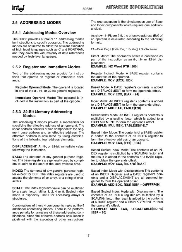
80386
2.5 ADDRESSING MODES
2.5.1 Addressing Modes Overview
The 80386 provides a total of 11 addressing modes for instructions to specify operands. The addressing modes are optimized to allow the efficient execution of high level languages such as C and FORTRAN, and they cover the vast majority of data references needed by high-level languages.
2.5.2 Register and Immediate Modes
Two of the addressing modes provide for instructions that operate on register or immediate operands:
Register Operand Mode: The operand is located in one of the 8-, 16- or 32-bit general registers.
Immediate Operand Mode: The operand is included in the instruction as part of the opcode.
2.5.3 32-Bit Memory Addressing Modes
The remaining 9 modes provide a mechanism for specifying the effective address of an operand. The linear address consists of two components: the segment base address and an effective address. The effective address is calculated by using combinations of the following four address elements:
DISPLACEMENT: An 8-, or 32-bit immediate value, following the instruction.
BASE: The contents of any general purpose register. The base registers are generally used by compilers to point to the start of the local variable area.
INDEX: The contents of any general purpose register except for ESP. The index registers are used to access the elements of an array, or a string of characters.
SCALE: The index register's value can be multiplied by a scale factor, either 1, 2, 4 or 8. Scaled index mode is especially useful for accessing arrays or structures.
Combinations of these 4 components make up the 9 additional addressing modes. There is no performance penalty for using any of these addressing combinations, since the effective address calculation is pipelined with the execution of other instructions.
17
The one exception is the simultaneous use of Base and Index components which requires one additional clock.
As shown in Figure 2-9, the effective address (EA) of an operand is calculated according to the following formula.
EA = Base Reg + (Index Reg' Scaling) + Displacement
Direct Mode: The operand's offset is contained as part of the instruction as an 8-, 16- or 32-bit displacement. EXAMPLE: INC Word PTR [500]
Register Indirect Mode: A BASE register contains the address of the operand. EXAMPLE: MOV [ECX], EDX
Based Mode: A BASE register's contents is added to a DISPLACEMENT to form the operands offset. EXAMPLE: MOV ECX, [EAX + 24]
Index Mode: An INDEX register's contents is added to a DISPLACEMENT to form the operands offset. EXAMPLE: ADD EAX, TABLE[ESIl
Scaled Index Mode: An INDEX register's contents is multiplied by a scaling factor which is added to a DISPLACEMENT to form the operands offset. EXAMPLE: IMUL EBX, TABLE[ESI*4],7
Based Index Mode: The contents of a BASE register is added to the contents of an INDEX register to form the effective address of an operand. EXAMPLE: MOV EAX, [ESI] [EBX]
Based Scaled Index Mode: The contents of an INDEX register is multiplied by a SCALING factor and the result is added to the contents of a BASE register to obtain the operands offset. EXAMPLE: MOV ECX, [EDX*S] [EAX]
Based Index Mode with Displacement: The contents of an INDEX Register and a BASE register's contents and a DISPLACEMENT are all summed together to form the operand offset. EXAMPLE: ADD EDX, [ESIl [EBP+OOFFFFFOH]
Based Scaled Index Mode with Displacement: The contents of an INDEX register are multiplied by a SCALING factor, the result is added to the contents of a BASE register and a DISPLACEMENT to form the operand's offset. EXAMPLE: MOV EAX, LOCALTABLE[EDI*4] [EBP+SO]
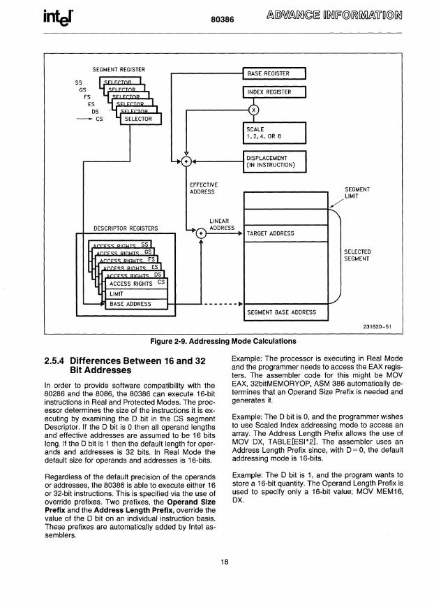
inter 80386
SEGMENT REGISTER .--------~ BASE REGISTER
SS GS
FS ES
DS
+ !+-____ -I DISPLACEMENT (IN INSTRUCTION)
EFFECTIVE ADDR ESS
LINEAR
/ SEGMENT LIMIT
DESCRIPTOR REGISTERS ADDRESS
ACCESS RIGHTS CS
LIMIT
• TARGET ADDRESS
SELECTED SEGMENT
BASE ADDRESS ------~ SEGMENT BASE ADDRESS
231630-51
Figure 2-9. Addressing Mode Calculations
2.5.4 Differences Between 16 and 32 Bit Addresses
In order to provide software compatibility with the 80286 and the 8086, the 80386 can execute 16-bit instructions in Real and Protected Modes. The processor determines the size of the instructions it is executing by examining the D bit in the CS segment Descriptor. If the D bit is ° then all operand lengths and effective addresses are assumed to be 16 bits long. If the D bit is 1 then the default length for operands and addresses is 32 bits. In Real Mode the default size for operands and addresses is 16-bits.
Regardless of the default precision of the operands or addresses, the 80386 is able to execute either 16 or 32-bit instructions. This is specified via the use of override prefixes. Two prefixes, the Operand Size Prefix and the Address Length Prefix, override the value of the D bit on an individual instruction basis. These prefixes are automatically added by Intel assemblers.
18
Example: The processor is executing in Real Mode and the programmer needs to access the EAX registers. The assembler code for this might be MOV EAX, 32bitMEMORYOP, ASM 386 automatically determines that an Operand Size Prefix is needed and generates it.
Example: The D bit is 0, and the programmer wishes to use Scaled Index addressing mode to access an array. The Address Length Prefix allows the use of MOV DX, TABLE[ESI*2]. The assembler uses an Address Length Prefix since, with D = 0, the default addressing mode is 16-bits.
Example: The D bit is 1, and the program wants to store a 16-bit quantity. The Operand Length Prefix is used to specify only a 16-bit value; MOV MEM16, DX.
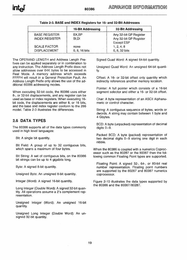
80386
Table 2-3. BASE and INDEX Registers for 16- and 32-Bit Addresses
16·Bit Addressing 32-Bit Addressing
BASE REGISTER BX,BP INDEX REGISTER SI,DI
SCALE FACTOR none DISPLACEMENT 0,8, 16 bits
The OPERAND LENGTH and Address Length Prefixes can be applied separately or in combination to any instruction. The Address Length Prefix does not allow addresses over 64K bytes to be accessed in Real Mode. A memory address which exceeds FFFFH will result in a General Protection Fault. An Address Length Prefix only allows the use of the additional 80386 addressing modes.
When executing 32-bit code, the 80386 uses either 8-, or 32-bit displacements, and any register can be used as base or index registers. When executing 16-bit code, the displacements are either 8, or 16 bits, and the base and index register conform to the 286 model. Table 2-3 illustrates the differences.
2.6 DATA TYPES
The 80386 supports all of the data types commonly used in high level languages:
Bit: A single bit quantity.
Bit Field: A group of up to 32 contiguous bits, which spans a maximum of four bytes.
Bit String: A set of contiguous bits, on the 80386 bit strings can be up to 4 gigabits long.
Byte: A signed 8-bit quantity.
Unsigned Byte: An unsigned 8-bit quantity.
Integer (Word): A signed 16-bit quantity.
Long Integer (Double Word): A signed 32-bit quantity. All operations assume a 2's complement representation.
Unsigned Integer (Word): An unsigned 16-bit quantity.
Unsigned Long Integer (Double Word): An unsigned 32-bit quantity.
19
Any 32-bit GP Register Any 32-bit GP Register Except ESP 1,2,4,8 0,8,32 bits
Signed Quad Word: A signed 64-bit quantity.
Unsigned Quad Word: An unsigned 64-bit quantity.
Offset: A 16- or 32-bit offset only quantity which indirectly references another memory location.
Pointer: A full pointer which consists of a 16-bit segment selector and either a 16- or 32-bit offset.
Char: A byte representation of an ASCII Alphanumeric or control character.
String: A contiguous sequence of bytes, words or dwords. A string may contain between 1 byte and 4 Gbytes.
BCD: A byte (unpacked) representation of decimal digits 0-9.
Packed BCD: A byte (packed) representation of two decimal digits 0-9 storing one digit in each nibble.
When the 80386 is coupled with a numerics Coprocessor such as the 80287 or the 80387 then the following common Floating Point types are supported.
Floating Point: A signed 32-, 64-, or 80-bit real number representation. Floating point numbers are supported by the 80287 and 80387 numerics coprocessor.
Figure 2-10 illustrates the data types supported by the 80386 and the 80387/80287.
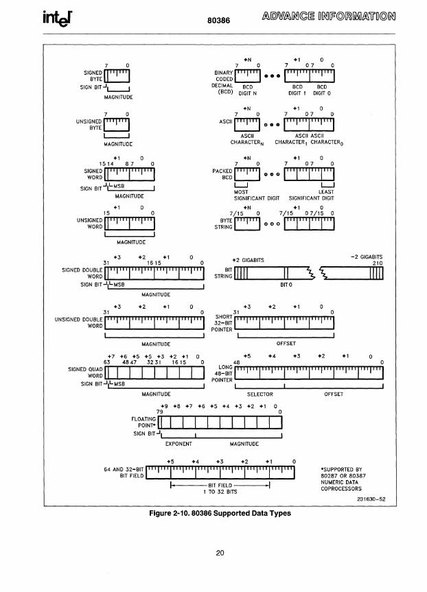
infef
7 0 SIGN ED rrrrrrrrl BYTE~
SIGN BIT.JL--)
MAGNITUDE
7 0 U NSIGN ED fT"1T""'1
BYTE L....:.-....J L--...J MAGNITUDE
+1 0 1514 87 0
s~~~g 11II Iii iii i i II iii SIGN BIT.J ... IL_M_S_B ___ ...1
MAGNITUDE
+1 0 15 0
UNS~~~g II iii iii Iii iii iii i I
MAGNITUDE
+3 +2 +1 0 31 1615 0
80386
+N 7 0
BINARY fT"1T""'1 ••• CODED L....:.-....J
DECIMAL BCD (BCD) DIGIT N
+N
+1 o 7 07 o l'ill'iililil'lIl
BCD BCD DIGIT 1 DIGIT 0
+1 o 7 0 7 07 0
ASCII ~ G • 0 I II i I II i I II i I II i I ASCII ASCII ASCII
CHARACTERN CHARACTER 1 CHARACTERO
+N 7 0
PACKED fT"1T""'1 • 0 • BCDL....:.-....J
L.J MOST SIGNIFICANT DIGIT
+1 0 7 07 0 I' iii iii I i Ii Iii i I
L.J LEAST
SIGNIFICANT DIGIT
+N +1 0 7/15 0 7 /15 0 7/15 0
ST:itJ~~ 000 IIi'rlll'"l'ill
+2 GIGABITS -2 GIGABITS 210
SIGNED DO~g~~ III i II iii iii Iii iii iii iii Iii iii iii STRI~I~ ILLlII.u.II __ ..&.I.II_~\ \~ __ ---i.I.111.I.I11I SIGN BIT .J ... IL....;M....;S....;B'--________ ....I BITO
MAGNITUDE
+3 +2 +1 o +3 +2 +1 o 31 0
UNSIGNED DO~g~~ I iii Iii II iii II i II iii Iii iii III iii I 31 0 i~.?B~i Iii i II iii iii Iii i III i II i III i I I i III
POINTER .... --....... --....... --_ ...... - ....... I ,
MAGNITUDE OFFSET
+7 +6 +5 +5 +3 +2 + 1 o +5 +4 +3 +2 +1 o 63 4847 3231 1615 o ~ 0
SIGNED ~~~gll:ll~I..I-........... - ........... -"' ............... 4i~~I~ Ii i 'I iii II' iii iii iii Iii i II iii iii I i I III i I1III1I i II
POINTER SIGN BIT.JLIL....;M;;,;S;.:B _________ ...I I' , MAGNITUDE SELECTOR OFFSET
+9 +8 +7 +6 +5 +4 +3 +2 +1 0 79 0
FL~~i~~~ 11;1-1--1..1--1_1...... ...... -'-....1...--1..--1_.1...-1 SIGN BIT.JL, ___ ....L _________ ---'
EXPONENT MAGNITUDE
+5 +4 +3 +2 + 1 0
64 AN~li~~E~~ I iii Iii II i i II iii I i III iii Iii iii iii iii Iii iii i i II iii ,. BIT FIELD .1
1 TO 32 BITS
Figure 2-10. 80386 Supported Data Types
20
'SUPPORTED BY 80287 OR 80387 NUMERIC DATA COPROCESSORS
231630-52

80386
2.7 MEMORY ORGANIZATION
2.7.1 Introduction ~emory on the 80386 is divided up into 8-bit quantities (bytes), 16-bit quantities (words), and 32-bit quantities (dwords). Words are stored in two consecutive bytes in memory with the low-order byte at the lowest address, the high order byte at the high address. Dwords are stored in four consecutive bytes in memory with the low-order byte at the lowest address, the high-order byte at the highest address. The address of a word or dword is the byte address of the low-order byte.
In addition to these basic data types the 386 supports two larger units of memory: pages and segments. Memory can be divided up into one or more variable length segments, which can be swapped to disk or shared between programs. Memory can also be organized into one or more 4K byte pages. Finally, both segmentation and paging can be combined, gaining the advantages of both systems. The 80386 supports both pages and segments in order to provide maximum flexibility to the system designer. Segmentation and paging are complementary. Segmentation is useful for organizing memory in logical modules, and as such is a tool for the application programmer, while pages are useful for the system programmer for managing the physical memory of a system.
2.7.2 Address Spaces The 80386 has three distinct address spaces: logical, linear, and physical. A logical address
EFFECTIVE ADDRESS CALCULATION
(also known as a virtual address) consists of a selector and an offset. A selector is the contents of a segment register. An offset is formed by summing all of the addressing components (BASE, INDEX, DISPLACEMENT) discussed in section 2.5.3 Memory Addressing Modes into an effective address. Since each task on 80386 has a maximum of 16K (214 -1) selectors, and offsets can be 4 gigabytes, (232
bits) this gives a total of 246 bits or 64 terabytes of logical address space per task. The programmer sees this virtual address space.
The segmentation unit translates the logical address space into a 32-bit linear address space. If the paging unit is not enabled then the 32-bit linear address corresponds to the physical address. The paging unit translates the linear address space into the physical address space. The physical address is what appears on the address pins.
The primary difference between Real Mode and Protected Mode is how the segmentation unit performs the translation of the logical address into the linear address. In Real Mode, the segmentation unit shifts the selector left four bits and adds the result to the offset to form the linear address. While in Protected Mode every selector has a linear base address associated with it. The linear base address is stored in one of two operating system tables (Le. the Local Descriptor Table or Global Descriptor Table). The selector's linear base address is added to the offset to form the final linear address.
Figure 2-11 shows the relationship between the various address spaces.
BE3- BEQ A31 - A2
32 0
PHYSICAL MEMORY
ADDRESS LOGICAL OR SEGMENTATION 1----'3~2;C+1 PAGING UNIT
14 VIRTUAL ADDRESS UNIT LINEAR (OPTIONAL USE) 15 32
SEGMENT REGISTER
t-"1'-;D;':ES;;C:;;'RI;;;PT;;:;O::-R --+L ____ ...J ADDRESS
INDEX
Figure 2-11. Address Translation
21
PHYSICAL ADDRESS L-.._......I
231630-53
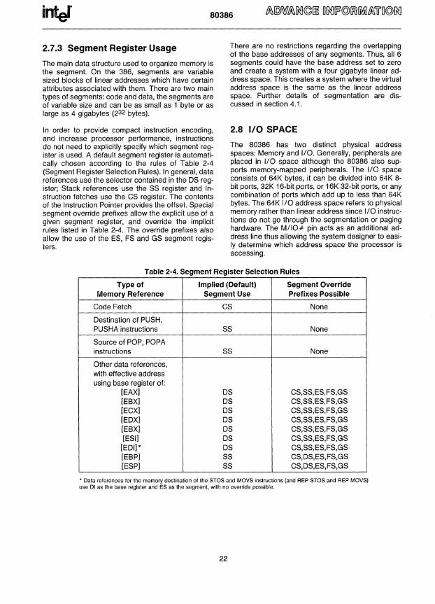
80386
2.7.3 Segment Register Usage
The main data structure used to organize memory is the segment. On the 386, segments are variable sized blocks of linear addresses which have certain attributes associated with them. There are two main types of segments: code and data, the segments are of variable size and can be as small as 1 byte or as large as 4 gigabytes (232 bytes).
In order to provide compact instruction encoding, and increase processor performance, instructions do not need to explicitly specify which segment register is used. A default segment register is automatically chosen according to the rules of Table 2-4 (Segment Register Selection Rules). In general, data references use the selector contained in the OS register; Stack references use the SS register and Instruction fetches use the CS register. The contents of the Instruction Pointer provides the offset. Special segment override prefixes allow the explicit use of a given segment register, and override the implicit rules listed in Table 2-4. The override prefixes also allow the use of the ES, FS and GS segment registers.
There are no restrictions regarding the overlapping of the base addresses of any segments. Thus, all 6 segments could have the base address set to zero and create a system with a four gigabyte linear address space. This creates a system where the virtual address space is the same as the linear address space. Further details of segmentation are discussed in section 4.1.
2.8 I/O SPACE
The 80386 has two distinct physical address spaces: Memory and 1/0. Generally, peripherals are placed in 1/0 space although the 80386 also supports memory-mapped peripherals. The 1/0 space consists of 64K bytes, it can be divided into 64K 8-bit ports, 32K 16-bit ports, or 16K 32-bit ports, or any combination of ports which add up to less than 64K bytes. The 64K 1/0 address space refers to physical memory rather than linear address since 1/0 instructions do not go through the segmentation or paging hardware. The M/IO# pin acts as an additional address line thus allowing the system designer to easily determine which address space the processor is accessing.
Table 2-4. Segment Register Selection Rules
Type of Implied (Default) Segment Override Memory Reference Segment Use Prefixes Possible
Code Fetch CS None
Destination of PUSH, PUSHA instructions SS None
Source of POP, POPA instructions SS None
Other data references, with effective address using base register of:
[EAX] OS CS,SS,ES,FS,GS [ESX] OS CS,SS,ES,FS,GS [ECX] OS CS,SS,ES,FS,GS [EOX] OS CS,SS,ES,FS,GS [ESX] OS CS,SS,ES,FS,GS [ESI] OS CS,SS,ES,FS,GS
[EOI]· DS CS,SS,ES,FS,GS [ESP] SS CS,DS,ES,FS,GS [ESP] SS CS,DS,ES,FS,GS
• Data references for the memory destination of the STaS and MaVS instructions (and REP STaS and REP MaVS) use 01 as the base register and ES as the segment, with no override possible.
22

80386
The 1/0 ports are accessed via the IN and OUT 1/0 instructions, with the port address supplied as an immediate 8-bit constant in the instruction or in the OX register. All 8- and 16-bit port addresses are zero extended on the upper address lines. The 1/0 instructions cause the M/IO# pin to be driven low.
1/0 port addresses 00F8H through OOFFH are reserved for use by Intel.
2.9 INTERRUPTS
2.9. i Interrupts and E}(cep~ions
Interrupts and exceptions alter the normal program flow, in order to handle external events, to report errors or exceptional conditions. The difference between interrupts and exceptions is that interrupts are used to handle asynchronous external events while exceptions handle instruction faults. Although a program can generate a software interrupt via an INT N instruction, the processor treats software interrupts as exceptions.
Hardware interrupts occur as the result of an external event and are classified into two types: maskable or non-maskable. Interrupts are serviced after the execution of the current instruction. After the interrupt handler is finished servicing the interrupt, execution proceeds with the instruction immediately after the interrupted instruction. Sections 2.9.3 and 2.9.4 discuss the differences between Maskable and Non-Maskable interrupts.
Exceptions are classified as faults, traps, or aborts depending on the way they are reported, and whether or not restart of the instruction causing the exception is supported. Faults are exceptions that are detected and serviced before the execution of the faulting instruction. A fault would occur in a virtual memory system, when the processor referenced a page or a segment which was not present. The operating system would fetch the page or segment from disk, and then the 80386 would restart the instruction. Traps are exceptions that are reported immediately after the execution of the instruction which caused the problem. User defined interrupts are examples of traps. Aborts are exceptions which do not permit the precise location of the instruction causing the exception to be determined. Aborts are used to report severe errors, such as a hardware error, or illegal values in system tables.
23
Thus, when an interrupt service routine has been completed, execution proceeds from the instruction immediately following the interrupted instruction. On the other hand, the return address from an exception fault routine will always point at the instruction causing the exception and include any leading instruction prefixes. Table 2-5 summarizes the possible interrupts for the 80386 and shows where the return address points.
The 80386 has the ability to handle up to 256 different interruptsl exceptions. In order to service the interrupts, a table with up to 256 interrupt vectors must be defined. The interrupt vectors are simply pointers to the appropriate interrupt service routine. In Real Mode (see section 3.1), the vectors are 4 byte quantities, a Code Segment plus a 16-bit offset; in Protected Mode, the interrupt vectors are 8 byte quantities, which are put in an Interrupt Descriptor Table (see section 4.1). Of the 256 possible interrupts, 32 are reserved for use by Intel, the remaining 224 are free to be used by the system designer.
2.9.2 Interrupt Processing
When an interrupt occurs the following actions happen. First, the current program address and the Flags are saved on the stack to allow resumption of the interrupted program. Next, an 8-bit vector is supplied to the 80386 which identifies the appropriate entry in the interrupt table. The table contains the starting address of the interrupt service routine. Then, the user supplied interrupt service routine is executed. Finally, when an IRET instruction is executed the old processor state is restored and program execution resumes at the appropriate instruction.
The 8-bit interrupt vector is supplied to the 80386 in several different ways: exceptions supply the interrupt vector internally; software INT instructions contain or imply the vector; maskable hardware interrupts supply the 8-bit vector via the interrupt acknowledge bus sequence. Non-Maskable hardware interrupts are assigned to interrupt vector 2.
2.9.3 Maskable Interrupt
Maskable interrupts are the most common way used by the 80386 to respond to asynchronous external hardware events. A hardware interrupt occurs when the INTR is pulled high and the Interrupt Flag bit (IF) is enabled. The processor only responds to interrupts between instructions, (REPeat String instruc-
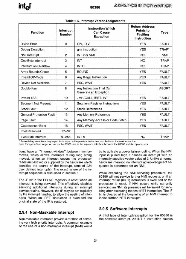
infef 80386
Table 2-5. Interrupt Vector Assignments
Instruction Which Return Address
Interrupt Points to Function Can Cause Type
Number Faulting Exception
Instruction
Divide Error 0 DIV,IDIV YES FAULT
Debug Exception 1 any instruction YES TRAP'
NMllnterrupt 2 INT 2 orNMI NO NMI
One Byte Interrupt 3 INT NO TRAP
Interrupt on Overflow 4 INTO NO TRAP
Array Bounds Check 5 BOUND YES FAULT
Invalid OP-Code 6 Any Illegal Instruction YES FAULT
Device Not Available 7 ESC, WAIT YES FAULT
Double Fault 8 Any Instruction That Can ABORT Generate an Exception
Invalid TSS 10 JMP, CALL, IRET, INT YES FAULT
Segment Not Present 11 Segment Register Instructions YES FAULT
Stack Fault 12 Stack References YES FAULT
General Protection Fault 13 Any Memory Reference YES FAULT
Page Fault 14 Any Memory Access or Code Fetch YES FAULT
Coprocessor Error 16 ESC, WAIT YES FAULT
Intel Reserved 17-32
Two Byte Interrupt 0-255 INTn NO TRAP • Some debug exceptIOns may report both traps on the prevIOUS Instruclion, and faults on the next Instruction. Note: Exception 9 no longer occurs on the 80386 due to the improved interface between the 80386 and its coprocessors.
tions, have an "interrupt window", between memory moves, which allows interrupts during long string moves). When an interrupt occurs the processor reads an 8-bit vector supplied by the hardware which identifies the source of the interrupt, (one of 224 user defined interrupts). The exact nature of the interrupt sequence is discussed in section 5.
The IF bit in the EFLAG registers is reset when an interrupt is being serviced. This effectively disables servicing additional interrupts during an interrupt service routine. However, the IF may be set explicitly by the interrupt handler, to allow the nesting of interrupts. When an IRET instruction is executed the original state of the IF is restored.
2.9.4 Non-Maskable Interrupt
Non-maskable interrupts provide a method of servicing very high priority interrupts. A common example of the use of a non-maskable interrupt (NMI) would
24
be to activate a power failure routine. When the NMI input is pulled high it causes an interrupt with an internally supplied vector value of 2. Unlike a normal hardware interrupt, no interrupt acknowledgment sequence is performed for an NMI.
While executing the NMI servicing procedure, the 80386 will not service further NMI requests, until an interrupt return (IRET) instruction is executed or the processor is reset. If NMI occurs while currently servicing an NMI, its presence will be saved f9r servicing after executing the first IRET instruction. The IF bit is cleared at the beginning of an NMI interrupt to inhibit further INTR interrupts.
2.9.5 Software Interrupts
A third type of interrupti exception for the 80386 is the software interrupt. An INT n instruction causes
80386
the processor to execute the interrupt service routine pointed to by the nth vector in the interrupt table.
A special case of the two byte software interrupt INT n is the one byte INT 3, or breakpoint interrupt. By inserting this one byte instruction in a program, the user can set breakpoints in his program as a debugging tool.
A final type of software interrupt, is the single step interrupt. It is discussed in section 2.12.
2.9.6 Interrupt and Exception Priorities
Interrupts are externally-generated events. Maskable Interrupts (on the INTR input) and Non-Maskable Interrupts (on the NMI input) are recognized at instruction boundaries. When NMI and maskable INTR are both recognized at the same instruction boundary, the 80386 invokes the NMI service routine first. If, after the NMI service routine has been invoked, maskable interrupts are still enabled, then the 80386 will invoke the appropriate interrupt service routine.
Table 2·6a. 80386 Priority for Invoking Service Routines in Case of
Simultaneous El(ternal Interrupts
1. NMI
2.INTR
Exceptions are internally-generated events. Exceptions are detected by the 80386 if, in the course of executing an instruction, the 80386 detects a problematic condition. The 80386 then immediately invokes the appropriate exception service routine. The state of the 80386 is such that the instruction causing the exception can be restarted. If the exception service routine has taken care of the problematic condition, the instruction will execute without causing the same exception.
It is possible for a single instruction to generate several exceptions (for example, transferring a single operand could generate two page faults if the operand location spans two "not present" pages). However, only one exception is generated upon each attempt to execute the instruction. Each exception service routine should correct its corresponding exception, and restart the instruction. In this manner, exceptions are serviced until the instruction executes successfully.
As the 80386 executes instructions, it follows a consistent cycle in checking for exceptions, as shown in Table 2-6b. This cycle is repeated as each instruc-
25
tion is executed, and occurs in parallel with instruction decoding and execution.
Table 2-6b. Sequence of Exception Checking
Consider the case of the 80386 having just completed an instruction. It then performs the following checks before reaching the point where the next instruction is completed:
1. Check for Exception 1 Traps from the instruction just completed (single-step via Trap Flag, or Data Breakpoints set in the Debug Registers).
2. Check for external NMI and INTR.
3. Check for Exception 1 Faults in the next instruction (Instruction Execution Breakpoint set in the Debug Registers for the next instruction).
4. Check for Segmentation Faults that prevented fetching the entire next instruction (exceptions 11 or 13).
5. Check for Page Faults that prevented fetching the entire next instruction (exception 14).
6. Check for Faults decoding the next instruction (exception 6 if illegal opcode; exception 6 if in Real Mode or in Virtual 8086 Mode and attempting to execute an instruction for Protected Mode only (see 4.6.4); or exception 13 if instruction is longer than 15 bytes, or privilege violation in Protected Mode (Le. not at IOPL or at CPL=O).
7. If WAIT opcode, check if TS=1 and MP=1 (exception 7 if both are 1).
B. If ESCAPE opcode for numeric coprocessor, check if EM = 1 or TS = 1 (exception 7 if either are 1).
9. If WAIT opcode or ESCAPE opcode for numeric coprocessor, check ERROR # input signal (exception 16 if ERROR # input is asserted).
10. Check in the following order for each memory reference required by the instruction:
a. Check for Segmentation Faults that prevent transferring the entire memory quantity (exceptions 11, 12, 13).
b. Check for Page Faults that prevent transferring the entire memory quantity (exception 14).
Note that the order stated supports the concept of the paging mechanism being "underneath" under segmentation mechanism. Therefore, for any given code or data reference in memory, segmentation exceptions are generated before paging exceptions are generated.

80386
2.9.7 Instruction Restart
The 80386 fully supports restarting all instructions after faults. If an exception is detected in the instruction to be executed (exception categories 4 through 10 in Table 2-6c), the 80386 invokes the appropriate exception service routine. The 80386 is in a state that permits restart of the instruction, for all cases but those in Table 2-6c. Note that all such cases are easily avoided by proper design of the operating system.
Table 2-6c. Conditions Preventing Instruction Restart
A. An instruction causes a task switch to a task whose Task State Segment is partially "not present". (An entirely "not present" TSS is restartable.) Partially present TSS's can be avoided either by keeping the TSS's of such tasks present in memory, or by aligning TSS segments to reside entirely within a single 4K page (for TSS segments of 4K bytes or less).
B. A coprocessor operand wraps around the top of a 64K-byte segment or a 4G-byte segment, and spans three pages, and the page holding the middle portion of the operand is "not present." This condition can be avoided by starting at a page boundary any segments containing coprocessor operands if the segments are approximately 64K-200 bytes or larger (i.e. large enough for wraparound of the coprocessor operand to possibly occur).
Note that these conditions are avoided by using the operating system designs mentioned in this table.
2.9.8 Double Fault
A Double Fault (exception 8) results when the processor attempts to invoke an exception service routine for the segment exceptions (10, 11, 12 or 13), but in the process of doing so, detects an exception other than a Page Fault (exception 14).
One other cause of generating a Double Fault (exception 8) is the 80386 detecting any other exception when it is attempting to invoke the Page Fault (exception 14) service routine (for example, if a Page Fault is detected when the 80386 attempts to invoke the Page Fault service routine). Of course in any functional system, not only in 80386-based systems, the entire page fault service routine must remain "present" in memory.
When a Double Fault occurs, the 80386 invokes the exception service routine for exception 8.
26
2.10 RESET AND INITIALIZATION
When the processor is initialized or Reset the registers have the values shown in Table 2-7. The 80386 will then start executing instructions near the top of physical memory, at location FFFFFFFOH. When the first InterSegment Jump or Call is executed, address lines A20-31 will drop low for CS-relative memory cycles, and the 80386 will only execute instructions in the lower one megabyte of physical memory. This allows the system designer to use a ROM at the top of physical memory to initialize the system and take care of Resets.
RESET forces the 80386 to terminate all execution and local bus activity. No instruction execution or bus activity will occur as long as Reset is active. Between 350 and 450 CLK2 periods after Reset becomes inactive the 80386 will start executing instructions at the top of physical memory.
Table 2·7. Register Values after Reset
Flag Word Machine Status Word (CRO) Instruction Pointer Code Segment Data Segment Stack Segment Extra Segment (ES) Extra Segment (FS) Extra Segment (GS) DX register
All other registers
NOTES:
UUUU0002H Note 1 UUUUUUUOH Note 2
OOOOFFFOH FOOOH Note 3 OOOOH OOOOH OOOOH OOOOH OOOOH
component and stepping ID Note 5
undefined Note 4
1. EFLAG Register. The upper 14 bits of the EFLAGS register are undefined, VM (Bit 17) and RF (BIT) 16 are a as are all other defined flag bits. 2. CRO: (Machine Status Word). All of the defined fields in the CRO are a (PG Bit 31, TS Bit 3, EM Bit 2, MP Bit 1, and PE Bit 0) except for ET Bit 4 (processor ex1ension type). The ET Bit is set during Reset according to the type of Coprocessor in the system. If the coprocessor is an 80387 then ET will be 1, if the coprocessor is an 80287 or no coprocessor is present then ET will be O. All other bits are undefined. 3. The Code Segment Register (CS) will have its Base Address set to FFFFOOOOH and Limit set to OFFFFH. 4. All undefined bits are Intel Reserved and should not be used. 5. OX register always holds component and stepping identifier (see 5.7). EAX register holds self-test signature if selftest was requested (see 5.6).
80386
2.11 TESTABILITY
2.11.1 Self-Test
The 80386 has the capability to perform a self-test. The self-test checks the function of all of the Control ROM and most of the non-random logic of the part. Approximately one-half of the 80386 can be tested during self-test.
Self-Test is initiated on the 80386 when the RESET pin transitions from HIGH to LOW, and the BUSY # pin is low. The self-test takes about 2'*19 clocks, or approximately 33 milliseconds with a 16 MHz 80386. At the completion of self-test the processor performs reset and begins normal operation. The part has successfully passed self-test if the contents of the EAX register are zero (0). If the results of EAX are not zero then the self-test has detected a flaw in the part.
2.11.2 TLB Testing
The 80386 provides a mechanism for testing the Translation Lookaside Buffer (TLB) if desired. This particular mechanism is unique to the 80386 and may not be continued in the same way in future processors. When testing the TLB it is recommended that paging be turned off (PG = 0 in CRO) to avoid interference with the test data being written to the TLB.
There are two TLB testing operations: 1) write entries into the TLB, and, 2) perform TLB lookups. Two Test Registers, shown in Figure 2-12, are provided for the purpose of testing. TR6 is the "test command register", and TR7 is the "test data register". The fields within these registers are defined below.
c: This is the command bit. For a write into TR6 to cause an immediate write into the TLB entry, write a o to this bit. For a write into TR6 to cause an immediate TLB lookup, write a 1 to this bit.
Linear Address: This is the tag field of the TLB. On a TLB write, a TLB entry is allocated to this linear address and the rest of that TLB entry is set per the value of TR7 and the value just written into TR6. On a TLB lookup, the TLB is interrogated per this value and if one and only one TLB entry matches, the rest of the fields of TR6 and TR7 are set from the matching TLB entry.
Physical Address: This is the data field of the TLB. On a write to the TLB, the TLB entry allocated to the linear address in TR6 is set to this value. On a TLB lookup, the data field (physical address) from the TLB is read out to here.
27
PL: On a TLB write, PL= 1 causes the REP field of TR7 to select which of four associative blocks of the TLB is to be written, but PL= 0 allows the internal pointer in the paging unit to select which TLB block is written. On a TLB lookup, the PL bit indicates whether the lookup was a hit (PL gets set to 1) or a miss (PL gets reset to 0).
V: The valid bit for this TLB entry. All valid bits can also be cleared by writing to CR3.
D, D#: The dirty bit for/from the TLB entry.
u, U #: The user bit for/from the TLB entry.
W, W#: The writable bit for/from the TLB entry.
For 0, U and W, both the attribute and its complement are provided as tag bits, to permit the option of a "don't care" on TLB lookups. The meaning of these pairs of bits is given in the following table:
)( )(# Effect During Value of Bit TLB Loolcup )( after TLB Write
0 0 Miss All Bit X Becomes Undefined 0 1 Match if X = 0 Bit X Becomes 0 1 0 Match if X = 1 Bit X Becomes 1 1 1 Match all Bit X Becomes Undefined
For writing a TLB entry:
1. Write TR7 for the desired physical address, PL and REP values.
2. Write TR6 with the appropriate linear address, etc. (be sure to write C = 0 for "write" command).
For looking up (reading) a TLB entry:
1. Write TR6 with the appropriate linear address (be sure to write C= 1 for "lookup" command).
2. Read TR7 and TR6. If the PL bit in TR7 indicates a hit, then the other values reveal the TLB contents. If PL indicates a miss, then the other values in TR7 and TR6 are indeterminate.
2.12 DEBUGGING SUPPORT
The 80386 provides several features which simplify the debugging process. The three categories of onchip debugging aids are:
1) the code execution breakpoint opcode (OCCH),
2) the single-step capability provided by the TF bit in the flag register, and
3) the code and data breakpoint capability provided by the Debug Registers DRO-3, DR6, and DR7.
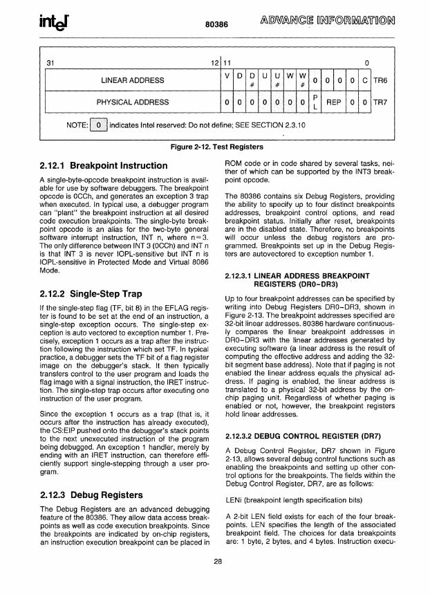
80386
31 12 11 0
LINEAR ADDRESS V 0 0 u u w w
0 01 0 0 C # # #
TR6
PHYSICAL ADDRESS 0 0 0 0 0 0 0 P
REP 0 0 L
TR?
NOTE: [£] indicates Intel reserved: Do not define; SEE SECTION 2.3.10
Figure 2-12. Test Registers
2.12.1 Breakpoint Instruction
A single·byte-opcode breakpoint instruction is available for use by software debuggers. The breakpoint opcode is OCCh, and generates an exception 3 trap when executed. In typical use, a debugger program can "plant" the breakpoint instruction at all desired code execution breakpoints. The single-byte breakpoint opcode is an alias for the two-byte general software interrupt instruction, INT n, where n = 3. The only difference between INT 3 (OCCh) and INT n is that INT 3 is never IOPL-sensitive but INT n is IOPL-sensitive in Protected Mode and Virtual 8086 Mode.
2.12.2 Single-Step Trap
If the single-step flag (TF, bit 8) in the EFLAG regis· ter is found to be set at the end of an instruction, a single-step exception occurs. The single-step exception is auto vectored to exception number 1. Precisely, exception 1 occurs as a trap after the instruction following the instruction which set TF. In typical practice, a debugger sets the TF bit of a flag register image on the debugger's stack. It then typically transfers control to the user program and loads the flag image with a signal instruction, the IRET instruction. The single-step trap occurs after executing one instruction of the user program.
Since the exception 1 occurs as a trap (that is, it occurs after the instruction has already executed), the CS:EIP pushed onto the debugger's stack points to the next unexecuted instruction of the program being debugged. An exception 1 handler, merely by ending with an IRET instruction, can therefore efficiently support single-stepping through a user program.
2.12.3 Debug Registers
The Debug Registers are an advanced debugging feature of the 80386. They allow data access breakpoints as well as code execution breakpoints. Since the breakpoints are indicated by on-chip registers, an instruction execution breakpoint can be placed in
28
ROM code or in code shared by several tasks, neither of which can be supported by the INT3 breakpoint opcode.
The 80386 contains six Debug Registers, providing the ability to specify up to four distinct breakpoints addresses, breakpoint control options, and read breakpoint status. Initially after reset, breakpoints are in the disabled state. Therefore, no breakpoints will occur unless the debug registers are programmed. Breakpoints set up in the Debug Registers are autovectored to exception number 1.
2.12.3.1 LINEAR ADDRESS BREAKPOINT REGISTERS (DRO-DR3)
Up to four breakpoint addresses can be specified by writing into Debug Registers DRO-DR3, shown in Figure 2-13. The breakpoint addresses specified are 32-bit linear addresses. 80386 hardware continuously compares the linear breakpoint addresses in DRO-DR3 with the linear addresses generated by executing software (a linear address is the result of computing the effective address and adding the 32-bit segment base address). Note that if paging is not enabled the linear address equals the physical address. If paging is enabled, the linear address is translated to a physical 32-bit address by the onchip paging unit. Regardless of whether paging is enabled or not, however, the breakpoint registers hold linear addresses.
2.12.3.2 DEBUG CONTROL REGISTER (DR?)
A Debug Control Register, DR? shown in Figure 2-13, allows several debug control functions such as enabling the breakpoints and setting up other control options for the breakpoints. The fields within the Debug Control Register, DR?, are as follows:
LENi (breakpoint length specification bits)
A 2-bit LEN field exists for each of the four breakpoints. LEN specifies the length of the associated breakpoint field. The choices for data breakpoints are: 1 byte, 2 bytes, and 4 bytes. Instruction execu-
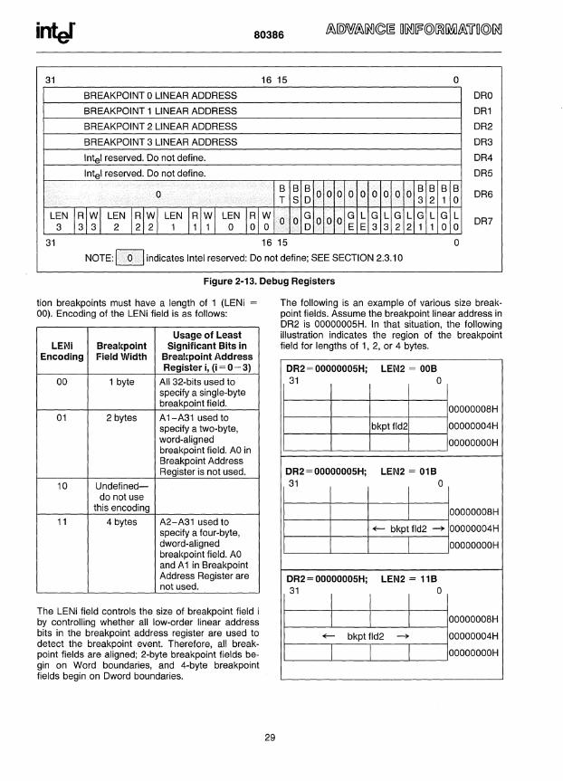
80386
31 16 15 0
BREAKPOINT 0 LINEAR ADDRESS ORO
BREAKPOINT 1 LINEAR ADDRESS DR1
BREAKPOINT 2 LINEAR ADDRESS DR2
BREAKPOINT 3 LINEAR ADDRESS DR3
Intel reserved. Do not define. DR4
Intel reserved. Do not define. DR5
0 B B B o 0 o 0 o 0 o 0 o B B B B DR6 T S 0 3 210
LEN I ~ I W I LEN I R I w I LEN I R I w I LEN I R I w 0 o G o 0 OG L G L G L G L G L DR? 333222111000 0 E E 3 322 1 100
31 16 15 0
NOTE: ~ indicates Intel reserved: Do not define; SEE SECTION 2.3.10
Figure 2-13. Debug Registers
tion breakpoints must have a length of 1 (LENi 00). Encoding of the LENi field is as follows:
Usage of Least LENi Brealcpoint Significant Bits in
Encoding Field Width Brea!cpoint Address Register i, (i = 0 - 3)
00 1 byte All 32-bits used to specify a single·byte breakpoint field.
01 2 bytes A1-A31 used to specify a two· byte, word·aligned breakpoint field. AD in Breakpoint Address Register is not used.
10 Undefined-do not use
this encoding
11 4 bytes A2-A31 used to specify a four·byte, dword-aligned breakpoint field. AD and A 1 in Breakpoint Address Register are not used.
The LENi field controls the size of breakpoint field i by controlling whether all low·order linear address bits in the breakpoint address register are used to detect the breakpoint event. Therefore, all break· point fields are aligned; 2·byte breakpoint fields begin on Word boundaries, and 4-byte breakpoint fields begin on Dword boundaries.
29
The following is an example of various size breakpoint fields. Assume the breakpoint linear address in DR2 is 00000005H. In that situation, the following illustration indicates the region of the breakpoint field for lengths of 1, 2, or 4 bytes.
DR2 = 00000005H; LEN2 = OOB
!= 31===! ==!b=kPt=fld2:! =:0 !:::::::;:
DR2 = 00000005H; 31
LEN2 = 01B
I o
I 00000008H
- bkpt fld2 ~ 00000004H
I OOOOOOOOH L-____ ~ ____ L-____ L_ __ ~
DR2 = 00000005H; LEN2 = 11B 31
I I I 0
I I 00000008H - bkpt fld2 --l> 00000004H
I I OOOOOOOOH

80386
RWi (memory access qualifier bits)
A 2-bit RW field exists for each of the four breakpoints. The 2-bit RW field specifies the type of usage which must occur in order to activate the associated breakpoint.
RW Usage Encoding Causing Breakpoint
00 Instruction execution only 01 Data writes only 10 Undefined-do not use this encoding 11 Data reads and writes only
RW encoding 00 is used to set up an instruction execution breakpoint. RW encodings 01 or 11 are used to set up write-only or read/write data breakpoints.
Note that instruction execution breakpoints are taken as faults (i.e. before the instruction executes), but data breakpoints are taken as traps (i.e. after the data transfer takes place).
Using LENi and RWi to Set Data Breakpoint i
A data breakpoint can be set up by writing the linear address into DRi (i = 0-3). For data breakpoints, RWi can = 01 (write-only) or 11 (write/read). LEN can = 00,01, or 11.
If a data access entirely or partly falls within the data breakpoint field, the data breakpoint condition has occurred, and if the breakpoint is enabled, an exception 1 trap will occur.
Using LENi and RWi to Set Instruction Execution Breakpoint i
An instruction execution breakpoint can be set up by writing address of the beginning of the instruction (including prefixes if any) into DRi (i = 0-3). RWi must = 00 and LEN must = 00 for instruction execution breakpoints.
If the instruction beginning at the breakpoint address is about to be executed, the instruction execution breakpoint condition has occurred, and if the breakpoint is enabled, an exception 1 fault will occur before the instruction is executed.
Note that an instruction execution breakpoint address must be equal to the beginning byte address of an instruction (including prefixes) in order for the instruction execution breakpoint to occur.
GD (Global Debug Register access detect)
The Debug Registers can only be accessed in Real Mode or at privilege level 0 in Protected Mode. The
30
GD bit, when set, provides extra protection against any Debug Register access even in Real Mode or at privilege level 0 in Protected Mode. This additional protection feature is provided to guarantee that a software debugger (or ICE-386) can have full control over the Debug Register resources when required. The GD bit, when set, causes an exception 1 fault if an instruction attempts to read or write any Debug Register. The GD bit is then automatically cleared when the exception 1 handler is invoked, allowing the exception 1 handler free access to the debug registers.
GE and LE (Exact data breakpoint match, global and local)
If either GE or LE is set, any data breakpoint trap will be reported exactly after completion of the instruction that caused the operand transfer. Exact reporting is provided by forcing the 80386 execution unit to wait for completion of data operand transfers before beginning execution of the next instruction.
If exact data breakpoint match is not selected, data breakpoints may not be reported until several instructions later or may not be reported at all. When enabling a data breakpoint, it is therefore recommended to enable the exact data breakpoint match.
When the 80386 performs a task switch, the LE bit is cleared. Thus, the LE bit supports fast task switching out of tasks, that have enabled the exact data breakpoint match for their task-local breakpoints. The LE bit is cleared by the processor during a task switch, to avoid having exact data breakpoint match enabled in the new task. Note that exact data breakpoint match must be re-enabled under software control.
The 80386 GE bit is unaffected during a task switch. The GE bit supports exact data breakpoint match that is to remain enabled during all tasks executing in the system.
Note that instruction execution breakpoints are always reported exactly, whether or not exact data breakpoint match is selected.
Gi and Li (breakpoint enable, global and local)
If either Gi or Li is set then the associated breakpoint (as defined by the linear address in DRi, the length in LENi and the usage criteria in RWi) is enabled. If either Gi or Li is set, and the 80386 detects the ith breakpoint condition, then the exception 1 handler is invoked.
When the 80386 performs a task switch to a new TSS, all Li bits are cleared. Thus, the Li bits support fast task switching out of tasks that use some tasklocal breakpoint registers. The Li bits are cleared by
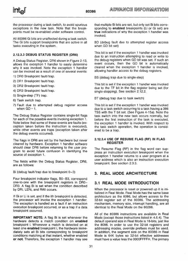
80386
the processor during a task switch, to avoid spurious exceptions in the new task. Note that the breakpoints must be re-enabled under software control.
All 80386 Gi bits are unaffected during a task switch. The Gi bits support breakpoints that are active in all tasks executing in the system.
2.12.3.3 DEBUG STATUS REGISTER (DR6)
A Debug Status Register, DR6 shown in Figure 2-13, allows the exception 1 handler to easily determine why it was invoked. Note the exception 1 handler can be invoked as a result of one of several events:
1) DRO Breakpoint fault/trap.
2) DR1 Breakpoint fault/trap.
3) DR2 Breakpoint fault/trap.
4) DR3 Breakpoint fault/trap.
5) Single-step (TF) trap.
6) Task switch trap.
7) Fault due to attempted debug register access when GD= 1.
The Debug Status Register contains single-bit flags for each of the possible events invoking exception 1. Note below that some of these events are faults (exception taken before the instruction is executed), while other events are traps (exception taken after the debug events occurred).
The flags in DR6 are set by the hardware but never cleared by hardware. Exception 1 handler software should clear DR6 before returning to the user program to avoid future confusion in identifying the source of exception 1.
The fields within the Debug Status Register, DR6, are as follows:
Bi (debug fault/trap due to breakpoint 0-3)
Four breakpoint indicator flags, BO-B3, correspond one-to-one with the breakpoint registers in DRODR3. A flag Bi is set when the condition described by DRi, LENi, and RWi occurs.
If Gi or Li is set, and if the ith breakpoint is detected, the processor will invoke the exception 1 handler. The exception is handled as a fault if an instruction execution breakpoint occurred, or as a trap if a data breakpoint occurred.
IMPORTANT NOTE: A flag Bi is set whenever the hardware detects a match condition on enabled breakpoint i. Whenever a match is detected on at least one enabled breakpoint i, the hardware immediately sets all Bi bits corresponding to breakpoint conditions matching at that instant, whether enabled or not. Therefore, the exception 1 handler may see
31
that multiple Bi bits are set, but only set Bi bits corresponding to enabled breakpoints (Li or Gi set) are true indications of why the exception 1 handler was invoked.
BD (debug fault due to attempted register access when GD bit set)
This bit is set if the exception 1 handler was invoked due to an instruction attempting to read or write to the debug registers when GD bit was set. If such an event occurs, then the GD bit is automatically cleared when the exception 1 handler is invoked, allowing handler access to the debug registers.
BS (debug trap due to single-step)
This bit is set if the exception 1 handler was invoked due to the TF bit in the flag register being set (for single-stepping). See section 2.12.2.
BT (debug trap due to task switch)
This bit is set if the exception 1 handler was invoked due to a task switch occurring to a task having a 386 TSS with the T bit set. (See Figure 4-15a). Note the task switch into the new task occurs normally, but before the first instruction of the task is executed, the exception 1 handler is invoked. With respect to the task switch operation, the operation is considered to be a trap.
2.12.3.4 USE OF RESUME FLAG (RF) IN FLAG REGISTER
The Resume Flag (RF) in the flag word can suppress an instruction execution breakpoint when the exception 1 handler returns to a user program at a user address which is also an instruction execution breakpoint. See section 2.3.3.
3. REAL MODE ARCHITECTURE
3.1 REAL MODE INTRODUCTION
When the processor is reset or powered up it is initialized in Real Mode. Real Mode has the same base architecture as the 8086, but allows access to the 32-bit register set of the 80386. The addressing mechanism, memory size, interrupt handling, are all identical to the Real Mode on the 80286.
All of the 80386 instructions are available in Real Mode (except those instructions listed in 4.6.4). The default operand size in Real Mode is 16-bits, just like the 8086. In order to use the 32-bit registers and addressing modes, override prefixes must be used. In addition, the segment size on the 80386 in Real Mode is 64K bytes so 32-bit effective addresses must have a value less the OOOOFFFFH. The primary
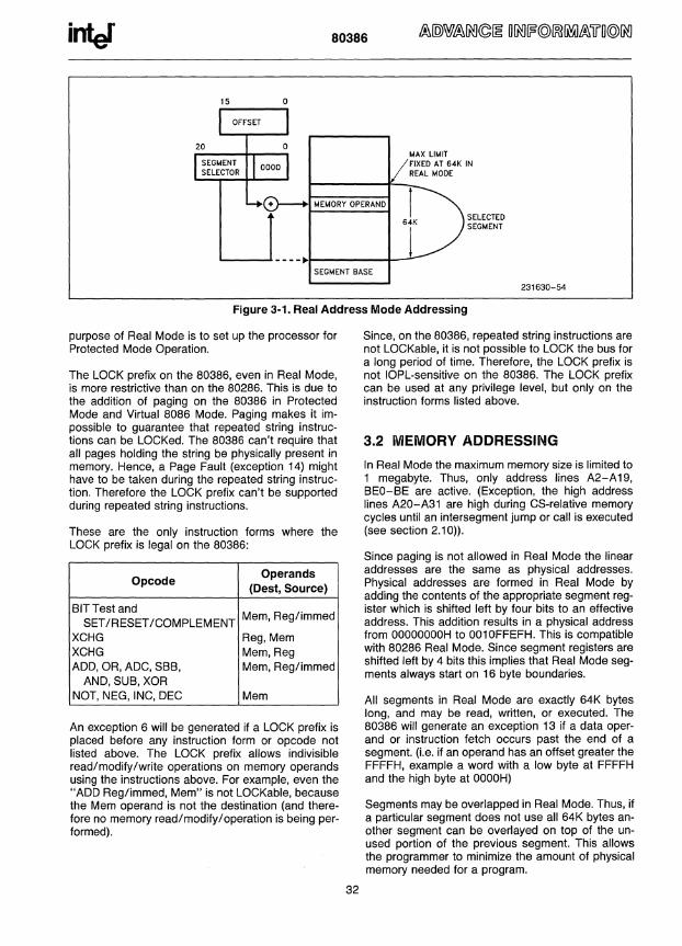
inter 80386
20 o MAX LIMIT FIXED AT 64K IN REAL MODE
1 64K
L-_---1 - - - - ~J_----+_--'-j ~ SELECTED SEGMENT
SEGMENT BASE
231630-54
Figure 3-1. Real Address Mode Addressing
purpose of Real Mode is to set up the processor for Protected Mode Operation.
The LOCK prefix on the 80386, even in Real Mode, is more restrictive than on the 80286. This is due to the addition of paging on the 80386 in Protected Mode and Virtual 8086 Mode. Paging makes it impossible to guarantee that repeated string instructions can be LOCKed. The 80386 can't require that all pages holding the string be physically present in memory. Hence, a Page Fault (exception 14) might have to be taken during the repeated string instruction. Therefore the LOCK prefix can't be supported during repeated string instructions.
These are the only instruction forms where the LOCK prefix is legal on the 80386:
Opcode Operands
(Dest, Source)
BIT Test and Mem, Reg/immed
SET/RESET/COMPLEMENT XCHG Reg, Mem XCHG Mem, Reg ADD, OR, ADC, SBB, Mem, Reg/immed
AND, SUB, XOR NOT, NEG, INC, DEC Mem
An exception 6 will be generated if a LOCK prefix is placed before any instruction form or opcode not listed above. The LOCK prefix allows indivisible read/modify/write operations on memory operands using the instructions above. For example, even the "ADD Reg/immed, Mem" is not LOCKable, because the Mem operand is not the destination (and therefore no memory read/modify/operation is being performed).
32
Since, on the 80386, repeated string instructions are not LOCKable, it is not possible to LOCK the bus for a long period of time. Therefore, the LOCK prefix is not IOPL-sensitive on the 80386. The LOCK prefix can be used at any privilege level, but only on the instruction forms listed above.
3.2 MEMORY ADDRESSING
In Real Mode the maximum memory size is limited to 1 megabyte. Thus, only address lines A2-A 19, BEO-BE are active. (Exception, the high address lines A20-A31 are high during CS-relative memory cycles until an intersegment jump or call is executed (see section 2.10)).
Since paging is not allowed in Real Mode the linear addresses are the same as physical addresses. Physical addresses are formed in Real Mode by adding the contents of the appropriate segment register which is shifted left by four bits to an effective address. This addition results in a physical address from OOOOOOOOH to 0010FFEFH. This is compatible with 80286 Real Mode. Since segment registers are shifted left by 4 bits this implies that Real Mode segments always start on 16 byte boundaries.
All segments in Real Mode are exactly 64K bytes long, and may be read, written, or executed. The 80386 will generate an exception 13 if a data operand or instruction fetch occurs past the end of a segment. (i.e. if an operand has an offset greater the FFFFH, example a word with a low byte at FFFFH and the high byte at OOOOH)
Segments may be overlapped in Real Mode. Thus, if a particular segment does not use all 64K bytes another segment can be overlayed on top of the unused portion of the previous segment. This allows the programmer to minimize the amount of physical memory needed for a program.

80386
3.3 RESERVED LOCATIONS
There are two fixed areas in memory which are reserved in Real address mode: system initialization area and the interrupt table area. Locations OOOOOH through 003FFH are reserved for interrupt vectors. Each one of the 256 possible interrupts has a 4-byte jump vector reserved for it. Locations FFFFFFFOH through FFFFFFFFH are reserved for system initialization.
3.4 INTIERRUPTS
Many of the exceptions shown in Table 2-5 and discussed in section 2.9 are not applicable to Real Mode operation, in particular exceptions 10, 11, 14, will not happen in Real Mode. Other exceptions have slightly different meanings in Real Mode; Table 3-1 identifies these exceptions.
3.5 SHUTDOWN AND HALT
The HL T instruction stops program execution and prevents the processor from using the local bus until restarted. Either NMI, INTR with interrupts enabled (IF = 1), or RESET will force the 80386 out of halt. If interrupted, the saved CS:IP will point to the next instruction after the HL T.
Shutdown will occur when a severe error is detected that prevents further processing. In Real Mode, shutdown can occur under two conditions:
An interrupt or an exception occur (Exceptions 8 or 13) and the interrupt vector is larger than the Interrupt Descriptor Table (i.e. There is not an interrupt handler for the interrupt).
A CALL, INT or PUSH instruction attempts to wrap around the stack segment when SP is not even. (e.g. pushing a value on the stack when SP = 0001 resulting in a stack segment greater than FFFFH)
An NMI input can bring the processor out of shutdown if the Interrupt Descriptor Table limit is large enough to contain the NMI interrupt vector (at least 0017H) and the stack has enough room to contain the vector and flag information (i.e. SP is greater than 0005H). Otherwise shutdown can only be exited via the RESET input.
4. PROTIECTIED MODIE ARCHITIECTURE
4.1 INTRODUCTION
The complete capabilities of the 80386 are unlocked when the processor operates in Protected Virtual Address Mode (Protected Mode). Protected Mode vastly increases the linear address space to four gigabytes (232 bytes) and allows the running of virtual memory programs of almost unlimited size (64 terabytes or 246 bytes). In addition Protected Mode allows the 80386 to run all of the existing 8086 and 80286 software, while providing a sophisticated memory management and a hardware-assisted protection mechanism. Protected Mode allows the use of additional instructions especially optimized for supporting multitasking operating systems. The base architecture of the 80386 remains the same, the registers, instructions, and addressing modes described in the previous sections are retained. The main difference between Protected Mode, and Real Mode from a programmer's view is the increased address space, and a different addressing mechanism.
Table 3·1
Function Interrupt Related Return Number Instructions Address Location
Interrupt table limit too small 8 INT Vector is not Before within table limit Instruction
CS, OS, ES, FF, GS 13 Word memory reference Before Segment overrun exception beyond offset = FFFFH. Instruction
An attempt to execute past the end of CS segment.
SS Segment overrun exception 12 Stack Reference Before beyond offset = FFFFH Instruction
33
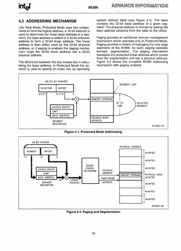
80386
4.2 ADDRESSING MECHANISM
Like Real Mode, Protected Mode uses two components to form the logical address, a 16-bit selector is used to determine the linear base address of a segment, the base address is added to a 32-bit effective address to form a 32-bit linear address. The linear address is then either used as the 32-bit physical address, or if paging is enabled the paging mechanism maps the 32-bit linear address into a 32-bit physical address.
The difference between the two modes lies in calculating the base address. In Protected Mode the selector is used to specify an index into an operating
48/32 BIT POINTER
system defined table (see Figure 4-1). The table contains the 32-bit base address of a given segment. The physical address is formed by adding the base address obtained from the table to the offset.
Paging provides an additional memory management mechanism which operates only in Protected Mode. Paging provides a means of managing the very large segments of the 80386. As such, paging operates beneath segmentation. The paging mechanism translates the protected linear address which comes from the segmentation unit into a physical address. Figure 4-2 shows the complete 80386 addressing mechanism with paging enabled.
SEGMENT LIMIT
~ MEMORY OPERAND r ACCESS RIGHTS
LIMIT
BASE ADDRESS
UP TO 4GB
1
SELECTED SEGMENT
SEGMENT DESCRIPTOR
SEGMENT BASE ADDRESS
Figure 4-1. Protected Mode Addressing
48 BIT POINTER , , PHYSICAL ADDRESS
I SEGMENT I OFFSET
15 31 I 0
80386
ACCESS RIGHTS PAGING MECHANISM PHYSICAL
LIMIT ,. ADDRESS
~ ~ LlNEAR~ MEMORY OPERAND
BASE ADDRESS PAGE FRAME
SEGMENT ADDRESS ADDRESS DESCRIPTOR
Figure 4-2. Paging and Segmentation
34
231630-55
! 4K BYTES
! 4K BYTES
! 4K BYTES
! PHYSICAL PAGE: 4K BYTES
! 4K BYTES
! 4K BYTES
! 4K BYTES
231630-56
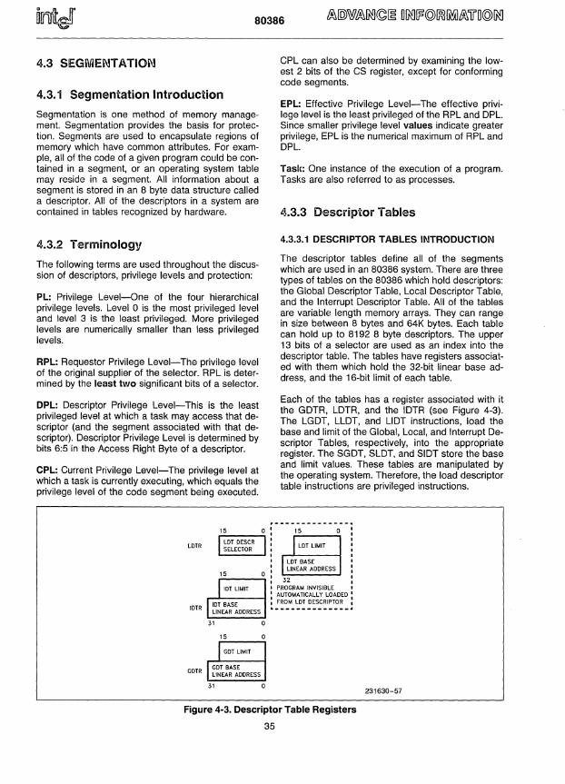
80386
4.3 SEGMENTATION
4.3.1 Segmentation Introduction
Segmentation is one method of memory management. Segmentation provides the basis for protection. Segments are used to encapsulate regions of memory which have common attributes. For example, all of the code of a given program could be contained in a segment, or an operating system table may reside in a segment. All information about a segment is stored in an 8 byte data structure called a descriptor. All of the descriptors in a system are contained in tables recognized by hardware.
4.3.2 Terminology
The following terms are used throughout the discussion of descriptors, privilege levels and protection:
PL: Privilege Level-One of the four hierarchical privilege levels. Level 0 is the most privileged level and level 3 is the least privileged. More privileged levels are numerically smaller than less privileged levels.
RPL: Requestor Privilege Level-The privilege level of the original supplier of the selector. RPL is determined by the least two significant bits of a selector.
DPL: Descriptor Privilege Level-This is the least privileged level at which a task may access that descriptor (and the segment associated with that descriptor). Descriptor Privilege Level is determined by bits 6:5 in the Access Right Byte of a descriptor.
CPL: Current Privilege Level-The privilege level at which a task is currently executing, which equals the privilege level of the code segment being executed.
15
LDTR I LOT DESCR SELECTOR
15
I lOT LIMIT
I lOT BASE IDTR LINEAR ADDRESS
31
15
I GOT LIMIT
I GOT BASE GDTR LINEAR ADDRESS
31
0
0
0
0
0
CPL can also be determined by examining the lowest 2 bits of the CS register, except for conforming code segments.
EPL: Effective Privilege Level-The effective privilege level is the least privileged of the RPL and DPL. Since smaller privilege level values indicate greater privilege, EPL is the numerical maximum of RPL and DPL.
Task: One instance of the execution of a program. Tasks are also referred to as processes.
4.3.3 Descriptor Tables
4.3.3.1 DESCRIPTOR TABLES INTRODUCTION
The descriptor tables define all of the segments which are used in an 80386 system. There are three types of tables on the 80386 which hold descriptors: the Global Descriptor Table, Local Descriptor Table, and the Interrupt Descriptor Table. All of the tables are variable length memory arrays. They can range in size between 8 bytes and 64K bytes. Each table can hold up to 8192 8 byte descriptors. The upper 13 bits of a selector are used as an index into the descriptor table. The tables have registers associated with them which hold the 32-bit linear base address, and the 16-bit limit of each table.
Each of the tables has a register associated with it the GDTR, LDTR, and the IDTR (see Figure 4-3). The LGDT, LLDT, and LlDT instructions, load the base and limit of the Global, Local, and Interrupt Descriptor Tables, respectively, into the appropriate register. The SGDT, SLOT, and SlOT store the base and limit values. These tables are manipulated by the operating system. Therefore, the load descriptor table instructions are privileged instructions.
--------------15 0
I LOT LIMIT
l LOT BASE LINEAR ADDRESS
32 PROGRAM INVISIBLE AUTOMATICALLY LOADED FROM LOT DESCRIPTOR
--------------
231630-57
Figure 4·3. Descriptor Table Registers
35
inter 80386
4.3.3.2 GLOBAL DESCRIPTOR TABLE
The Global Descriptor Table (GDT) contains descriptors which are possibly available to all of the tasks in a system. The GDT can contain any type of segment descriptor except for descriptors which are used for servicing interrupts (Le. interrupt and trap descriptors). Every 3B6 system contains a GDT. Generally the GDT contains code and data segments used by the operating systems and task state segments, and descriptors for the LDTs in a system.
The first slot of the Global Descriptor Table corresponds to the null selector and is not used. The null selector defines a null pointer value.
4.3.3.3 LOCAL DESCRIPTOR TABLE
LDTs contain descriptors which are associated with a given task. Generally, operating systems are designed so that each task has a separate LDT. The LDT may contain only code, data, stack, task gate, and call gate descriptors. LDTs provide a mechanism for isolating a given task's code and data segments from the rest of the operating system, while the GDT contains descriptors for segments which are common to all tasks. A segment cannot be accessed by a task if its segment descriptor does not exist in either the current LDT or the GDT. This provides both isolation and protection for a task's segments, while still allowing global data to be shared among tasks.
Unlike the 6 byte GDT or IDT registers which contain a base address and limit, the visible portion of the LDT register contains only a 16-bit selector. This selector refers to a Local Descriptor Table descriptor in the GDT.
31
4.3.3.4 INTERRUPT DESCRIPTOR TABLE
The third table needed for B03B6 systems is the Interrupt Descriptor Table. (See Figure 4-4.) The IDT contains the descriptors which point to the location of up to 256 interrupt service routines. The IDT may contain only task gates, interrupt gates, and trap gates. The IDT should be at least 256 bytes in size in order to hold the descriptors for the 32 Intel Reserved Interrupts. Every interrupt used by a system must have an entry in the IDT. The IDT entries are referenced via INT instructions, external interrupt vectors, and exceptions. (See 2.9 Interrupts).
I 32
CPU S " 0
~ lOT BASE
0
"\, MEMORY "\.,., r ~
GATE FOR INTERRUPT #n
GATE FOR INTERRUPT #n·1
· · · GATE FOR INTERRUPT #1
GATE FOR INTERRUPT #0
-C ~
INTERRUPT DESCRIPTOR TABLE (IDT)
231630-58
Figure 4-4. Interrupt Descriptor Table Register Use
4.3.4 Descriptors
4.3.4.1 DESCRIPTOR ATTRIBUTE BITS
The object to which the segment selector points to is called a descriptor. Descriptors are eight byte quantities which contain attributes about a given region of linear address space (Le. a segment). These
o BYTE ADDRESS
SEGMENT BASE 15 ... 0 SEGMENT LIMIT 15 ... 0 o
BASE 31 ... 24 G D 0 0 LIMIT
P DPL S TYPE A BASE
19 ... 16 I I I
23 ... 16 +4
BASE Base Address of the segment LIMIT The length of the segment P Present Bit 1 = Present 0 = Not Present DPL Descriptor Privilege Level 0-3 S Segment Descriptor 0 = System Descriptor 1 = Code or Data Segment Descriptor TYPE Type of Segment A Accessed Bit G Granularity Bit t = Segment length is page granular 0 = Segment length is byte granular D Default Operation Size (recognized in code segment descriptors only) 1 = 32·bit segment 0 = 16·bit segment o Bit must be zero (0) for compatibility with future processors
Figure 4·5. Segment Descriptors
36
80386
attributes include the 32-bit base linear address of the segment, the 20-bit length and granularity of the segment, the protection level, read, write or execute privileges, the default size of the operands (16-bit or 32-bit), and the type of segment. All of the attribute information about a segment is contained in 12 bits in the segment descriptor. Figure 4-5 shows the general format of a descriptor. All segments on the 80386 have three attribute fields in common: the P bit, the DPL bit, and the S bit. The Present P bit is 1 if the segment is loaded in physical memory, if P = 0 then any attempt to access this segment causes a not present exception (exception 11). The Descriptor Privilege Level DPL is a two-bit field which specifies the protection level 0-3 associated with a segment.
The 80386 has two main categories of segments system segments and non-system segments (for code and data). The segment S bit in the segment descriptor determines if a given segment is a system segment or a code or data segment. If the S bit is 1 then the segment is either a code or data segment, if it is 0 then the segment is a system segment.
4.3.4.2386 CODE, DATA DESCRIPTORS (S= 1)
Figure 4-6 shows the general format of a code and data descriptor and Table 4-1 illustrates how the bits in the Access Rights Byte are interpreted.
31 o SEGMENT BASE 15 ... 0 SEGMENT LIMIT 15 ... 0 o
LIMIT ACCESS BASE
BASE 31 ... 24 G 0 0 0 19 ... 16
RIGHTS 23 ... 16
BYTE +4
DIB 1 ~ Default Instructions Attnbutes are 32·81ts o ~ Default Instruction Attributes are 16·8its
G Granulanty Bit 1 - Segment length IS page granular o ~ Segment length is byte granular
Type Field Definition
Bit must be zero (0) for compatibility with future processors
Figure 4-6. Segment Descriptors
Table 4-1. Access Rights Byte Definition for Code and Data Descriptions
Bit Name Function
Position
7 Present (P) P = 1 Segment is mapped into physical memory. P = 0 No mapping to physical memory exits, base and limit are
not used. 6-5 Descriptor Privilege Segment privilege attribute used in privilege tests.
Level (DPL) 4 Segment Descrip- S = 1 Code or Data (includes stacks) segment descriptor
tor (S) S=O System Segment Descriptor or Gate Descriptor
3 Executable (E) E ~ 0 D'''';ptm typ' ;, data "gm,nt r 2 Expansion Direc- ED = 0 Expand up segment, offsets must be ,,; limit. Data
tion (ED) ED = 1 Expand down segment, offsets must be > limit. Segment 1 Writeable (W) W = 0 Data segment may not be written into. (S = 1,
W = 1 Data segment may be written into. E = 0)
3 Executable (E) E = 1 Descriptor type is code segment:
r 2 Conforming (C) C = 1 Code segment may only be executed Code when CPL :2: DPL and CPL Segment remains unchanged. (S = 1,
1 Readable (R) R=O Code segment may not be read. E = 1) R = 1 Code segment may be read.
0 Accessed (A) A=O Segment has not been accessed. A=1 Segment selector has been loaded into segment register
or used by selector test instructions.
37

80386
Code and data segments have several descriptor fields in common. The accessed A bit is set whenever the processor accesses a descriptor. The A bit is used by operating systems to keep usage statistics on a given segment. The G bit, or granularity bit, specifies if a segment length is byte-granular or page-granular. 80386 segments can be one megabyte long with byte granularity (G = 0) or four gigabytes with page granularity (G = 1), (i.e., 220 pages each page is 4K bytes in length). The granularity is totally unrelated to paging. A 80386 system can consist of segments with byte granularity, and page granularity, whether or not paging is enabled.
The executable E bit tells if a segment is a code or data segment. A code segment (E = 1 , S = 1) may be execute-only or execute/read as determined by the Read R bit. Code segments are execute only if R = 0, and execute/read if R = 1. Code segments may never be written into.
NOTE: Code segments may be modified via aliases. Aliases are writeable data segments which occupy the same range of linear address space as the code segment.
The D bit indicates the default length for operands and effective addresses. If D = 1 then 32-bit operands and 32-bit addressing modes are assumed. If D = 0 then 16-bit operands and 16-bit addressing modes are assumed. Therefore all existing 286 code segments will execute on the 80386 assuming the D bit is set o.
Another attribute of code segments is determined by the conforming C bit. Conforming segments, C = 1, can be executed and shared by programs at different privilege levels. (See section 4.4 Protection.)
31
SEGMENT BASE 15 ... 0
BASE 31 ... 24
Type
o 1 2 3 4 5 6 7
Defines
Invalid Available 286 TSS LDT Busy 286 TSS 286 Call Gate Task Gate (for 286 or 386 Task) 286 Interrupt Gate 286 Trap Gate
16
LIMIT 19 ... 16
Segments identified as data segments (E = 0, S = 1) are used for two types of 80386 segments: stack and data segments. The expansion direction (ED) bit specifies if a segment expands downward (stack) or upward (data). If a segment is a stack segment all offsets must be greater than the segment limit. On a data segment all offsets must be less than or equal to the limit. In other words, stack segments start at the base linear address plus the maximum segment limit and grow down to the base linear address plus the limit. On the other hand, data segments start at the base linear address and expand to the base linear address plus limit.
The write W bit controls the ability to write into a segment. Data segments are read-only if W = O. The stack segment must have W = 1.
The B bit controls the size of the stack pointer register. If B = 1, then PUSHes, POPs, and CALLs all use the 32-bit ESP register for stack references and assume an upper limit of FFFFFFFFH. If B = 0, stack instructions all use the 16-bit SP register and assume an upper limit of FFFFH.
4.3.4.3 SYSTEM DESCRIPTOR FORMATS
System segments describe information about operating system tables, tasks, and gates. Figure 4-7 shows the general format of system segment descriptors, and the various types of system segments. 80386 system descriptors contain a 32-bit base linear address and a 20-bit segment limit. 80286 system descriptors have a 24-bit base address and a 16-bit segment limit. 80286 system descriptors are identified by the upper 16 bits being all zero.
o SEGMENT LIMIT 15 ... 0 o
P
Type
8 9 A B C D E F
Defines
Invalid
TYPE
Available 386 TSS Undefined (Intel Reserved) Busy 386 TSS 386 Call Gate Undefined (Intel Reserved) 386 Interrupt Gate 386 Trap Gate
BASE 23 ... 16
+4
Figure 4·7. System Segments Descriptors
38
80386
4.3.4.4 LDT DESCRIPTORS (S = 0, TYPE = 2)
LDT descriptors (S = 0 TYPE = 2) contain information about Local Descriptor Tables. LDTs contain a table of segment descriptors, unique to a particular task. Since the instruction to load the LDTR is only available at privilege level 0, the DPL field is ignored. LDT descriptors are only allowed in the Global Descriptor Table (GDT).
4.3.4.5 TSS DESCRIPTORS (5=0, TVPE= 1, 3, 9, B)
A Task State Segment (TSS) descriptor contains information about the location, size, and privilege level of a Task State Segment (TSS). A TSS in turn is a special fixed format segment which contains all the state information for a task and a linkage field to permit nesting tasks. The TYPE field is used to indicate whether the task is currently BUSY (Le. on a chain of active tasks) or the TSS is available. The TYPE field also indicates if the segment contains a 286 or a 386 TSS. The Task Register (TR) contains the selector which points to the current Task State Segment.
4.3.4.6 GATE DESCRIPTORS (S=O, TYPE=4-7, C, F)
Gates are used to control access to entry points within the target code segment. The various types of
31 24 16
gate descriptors are call gates, task gates, interrupt gates, and trap gates. Gates provide a level of indirection between the source and destination of the control transfer. This indirection allows the processor to automatically perform protection checks. It also allows system designers to control entry points to the operating system. Call gates are used to change privilege levels (see section 4.4 Protection), task gates are used to perform a task switch, and interrupt and trap gates are used to specify interrupt service routines.
Figure 4-8 shows the format of the four types of gate descriptors. Call gates are primarily used to transfer program control to a more privileged level. The call gate descriptor consists of three fields: the access byte, a long pointer (selector and offset) which points to the start of a routine and a word count which specifies how many parameters are to be copied from the caller's stack to the stack of the called routine. The word count field is only used by call gates when there is a change in the privilege level, other types of gates ignore the word count field.
I nterrupt and trap gates use the destination selector and destination offset fields of the gate descriptor as a pointer to the start of the interrupt or trap handler routines. The difference between interrupt gates and trap gates is that the interrupt gate disables interrupts (resets the IF bit) while the trap gate does not.
8 5 o SELECTOR OFFSET 15 ... 0 o
OFFSET 31 ... 16
Name Type
P
Value 4 5 6 7 C E F o
P DPL
Gate Descriptor Fields Description
286 call gate Task gate (for 286 or 386 task) 286 interrupt gate 286 trap gate 386 call gate 386 interrupt gate 386 trap gate Descriptor contents are not valid Descriptor contents are valid
WORD 0 TYPE 0 0 0 COUNT +4
4 ... 0
DPL-Ieast privileged level at which a task may access the gate. WORD COUNT 0-31-the number of parameters to copy from caller's stack to the called procedure's stack. The parameters are 32-bit quantities for 386 gates, and 16-bit quantities for 286 gates.
DESTINATION 16-bit Selector to the target code segment SELECTOR selector or
DESTINATION OFFSET
offset 16-bit 286 32-bit 386
Selector to the target task state segment for task gate
Entry point within the target code segment
Figure 4·8. Gate Descriptor Formats
39

intJ 80386
Task gates are used to switch tasks. Task gates may only refer to a task state segment (see section 4.4.6 Task Switching) therefore only the destination selector portion of a task gate descriptor is used, and the destination offset is ignored.
Exception 13 is generated when a destination selector does not refer to a correct descriptor type, i.e., a code segment for an interrupt, trap or call gate, a TSS for a task gate.
The access byte format is the same for all gate descriptors. P = 1 indicates that the gate contents are valid. P = 0 indicates the contents are not valid and causes exception 11 if referenced. DPL is the descriptor privilege level and specifies when this descriptor may be used by a task (see section 4.4 Protection). The S field, bit 4 of the access rights byte, must be 0 to indicate a system control descriptor. The type field specifies the descriptor type as indicated in Figure 4-8.
4.3.4.7 DIFFERENCES BETWEEN 386 AND 286 DESCRIPTORS
In order to provide operating system compatibility between the 80286 and 80386, the 386 supports all of the 80286 segment descriptors. Figure 4-9 shows the general format of an 80286 system segment descriptor. The only differences between 286 and 386 descriptor formats are that the values of the type fields, and the limit and base address fields have been expanded for the 386. The 80286 system segment descriptors contained a 24-bit base address and 16-bit limit, while the 386 system segment descriptors have a 32-bit base address, a 20-bit limit field, and a granularity bit.
By supporting 80286 system segments the 80386 is able to execute 286 application programs on a 80386 operating system. This is possible because the processor automatically understands which de-
31
SEGMENT BASE 15 ... 0
Intel Reserved Set to 0
BASE LIMIT P
Base Address of the segment The length of the segment Present Bit 1 = Present 0 = Not Present
scriptors are 286-style descriptors and which descriptors are 386-style descriptors. In particular, if the upper word of a descriptor is zero, then that descriptor is a 286-style descriptor.
The only other differences between 286-style descriptors and 386 descriptors is the interpretation of the word count field of call gates and the B bit. The word count field specifies the number of 16-bit quantities to copy for 286 call gates and 32-bit quantities for 386 call gates. The B bit controls the size of PUSHes when using a call gate; if B = 0 PUSHes are 16 bits, if B = 1 PUSHes are 32 bits.
4.3.4.8 SELECTOR FIELDS
A selector in Protected Mode has three fields: Local or Global Descriptor Table Indicator (TI), Descriptor Entry Index (Index), and Requestor (the selector's) Privilege Level (RPL) as shown in Figure 4-10. The TI bits select one of two memory-based tables of descriptors (the Global Descriptor Table or the Local Descriptor Table). The Index selects one of 8K descriptors in the appropriate descriptor table. The RPL bits allow high speed testing of the selector's privilege attributes.
4.3.4.9 SEGMENT DESCRIPTOR CACHE
In addition to the selector value, every segment register has a segment descriptor cache register associated with it. Whenever a segment register's contents are changed, the 8-byte descriptor associated with that selector is automatically loaded (cached) on the chip. Once loaded, all references to that segment use the cached descriptor information instead of reaccessing the descriptor. The contents of the descriptor cache are not visible to the programmer. Since descriptor caches only change when a segment register is changed, programs which modify the descriptor tables must reload the appropriate segment registers after changing a descriptor's value.
SEGMENT LIMIT 15 ... 0
P \ DPL lsi TYPE \ BASE 23 ... 16
DPL S TYPE
.. DeSCriptor PnVllege Level 0-3 System Descriptor 0 = System 1 = User Type of Segment
o o
+4
Figure 4-9. 286 Code and Data Segment Descriptors
40

SEGMENT REGISTER
80386
SELECTOR
15 4 3 2 1 a
I 0 I 0 ---- a I a 11 11 nil R~L I . INDEX
N
6
5
4
~
2
1
a
. TABLE INDICATOR
TI-1
A
DESC~IPTOR
LOCAL DESCRIPTOR
TABLE
N
DESCRIPTOR NUMBER
6
5
4
3
2
1
0
TI-a!
NULL
GLOBAL DESCRIPTOR
TABLE
Figure 4·10. El(smple Descriptor Selection
41
231630-59

inter 80386
4.3.4.10 SEGMENT DESCRIPTOR REGISTER SETTINGS
The contents of the segment descriptor cache vary depending on the mode the 80386 is operating in. When operating in Real Address Mode, the segment base, limit, and other attributes within the segment cache registers are defined as shown in Figure 4-11 .
For compatiblity with the 8086 architecture, the base is set to sixteen times the current selector value, the limit is fixed at OOOOFFFFH, and the attributes are fixed so as to indicate the segment is present and fully usable. In Real Address Mode, the internal "privilege level" is always fixed to the highest level, level 0, so I/O and other privileged opcodes may be executed.
SEGMENT DESCRIPTOR CACHE REGISTER CONTENTS
32 - BIT BASE
(UPDATED DURING SELECTOR LOAD INTO SEGMENT REGISTER)
32 - BIT LIMIT
(FIXED)
OTHER ATIRIBUTES
(FIXED)
CONFORMING PRIVILEGE -----------------------, STACKSIZE----------------------------, EXECUTABLE------------------------, WRITEABLE-----------------------, R~DABLE-----------------------,
EXPANSION DIRECTION
GRANULARITY 1 ACCESSED 1 ~~~~~~~E _L~~E~ ___ ~A~~ ___________ ~I~I! ___ ttl _ __ CS 16X CURRENT CS SELECTOR" OOOOFFFFH Y 0 Y B U Y Y Y - N
SS 16X CURRENT SS SELECTOR OOOOFFFFH Y 0 Y B U Y Y N W -DS 16X CURRENT DS SELECTOR OOOOFFFFH Y 0 Y B U Y Y N - -ES 16X CURRENT ES SELECTOR OOOOFFFFH Y 0 Y B U Y Y N - -FS 16X CURRENT FS SELECTOR OOOOFFFFH Y 0 Y B U Y Y N - -GS 16X CURRENT GS SELECTOR OOOOFFFFH Y 0 Y B U Y Y N - -
231630-60
'Except the 32-bit CS base is initialized to FFFFFOOOH after reset until first intersegment control transfer (e.g. intersegment CALL. or intersegment JMP, or INT). (See Figure 4-13 Example.)
Key: Y = yes N = no o = privilege level 0 1 = privilege level 1 2 = privilege level 2 3 = privilege level 3 U = expand up
D = expand down B = byte granularity P = page granularity W = push/pop 16-bit words F = push/pop 32·bit dwords - = does not apply to that segment cache register
Figure 4-11. Segment Descriptor Caches for Real Address Mode (Segment Limit and Attributes are Fixed)
42
80386
When operating in Protected Mode, the segment base, limit, and other attributes within the segment cache registers are defined as shown in Figure 4-12. In Protected Mode, each of these fields are defined
according to the contents of the segment descriptor indexed by the selector value loaded into the segment register.
SEGMENT DESCRIPTOR CACHE REGISTER CONTENTS
32 - BIT BASE
(UPDATED DURING SELECTOR LOAD INTO
SEGMENT REGISTER)
32 - BIT LIMIT
(UPDATED DURING SELECTOR LOAD INTO
SEGMENT REGISTER)
OTHER ATTRIBUTES
(UPDATED DURING SELECTOR LOAD INTO
SEGMENT REGISTER)
CONFORMING PRIVILEGE -----------------------., STACK SIZE-----------------------, EXECUTABLE-----------------------,
WRITEABLE --------------------~ READABLE--------------------,
EXPANSION DIRECTION 1 GRANULARITY
ACCESSED 1 ~:!~~~~E _ L~~E~ ~~s~ ___________ :I~I! ______ ~ J 1 ___ _ CS BASE PER SEG DESCR LIMIT PER SEG DESCR P d d d d d N
SS BASE PER SEG DESCR LIMIT PER SEG DESCR P d d d d r w
OS
ES
FS
GS
Key: Y = fixed yes N = fixed no
BASE PER SEG DESCR
BASE PER SEG DESCR
BASE PER SEG DESCR
BASE PER SEG DESCR
d = per segment descriptor
LIMIT PER SEG DESCR p d d
LIMIT PER SEG DESCR p d d
LIMIT PER SEG DESCR P d d
LIMIT PER SEG DESCR p d d
p = per segment descriptor; descriptor must indicate "present" to avoid exception 11 (exception 12 in case of SS)
d
d
d
d
r = per segment descriptor, but descriptor must indicate "readable" to avoid exception 13 (special case for SS)
w = per segment descriptor, but descriptor must indicate "writable" to avoid exception 13 (special case for SS)
- = does not apply to that segment cache register
d d d
d d d
d d d
d d d
Y - d
N d -N - -N - -N - -N - -
231630-61
Figure 4-12. Segment Descriptor Caches for Protected Mode (Loaded per Descriptor)
43

inter 80386
When operating in a Virtual 8086 Mode within the Protected Mode, the segment base, limit, and other attributes within the segment cache registers are defined as shown in Figure 4-13. For compatibility with the 8086 architecture, the base is set to sixteen times the current selector value, the limit is fixed at
OOOOFFFFH, and the attributes are fixed so as to indicate the segment is present and fully usable. The virtual program executes at lowest privilege level, level 3, to allow trapping of all IOPL-sensitive instructions and level-a-only instructions.
SEGMENT DESCRIPTOR CACHE REGISTER CONTENTS
32- BIT BASE
(UPDATED DURING SELECTOR LOAD INTO SEGMENT REGISTER)
32 - BIT LIMIT
(FIXED)
OTHER ATIRIBUTES
(FIXED)
CONFORMING PRIVILEGE ----------------------, STACK SIZE-----------------------. EXECUTABLE----------------------, WRITEABLE---------------------, READABLE--------------------, EXPANSION DIRECTION
GRANULARITY 1 ACCESSED 1 ~~?~~~~E _ L~~E~ ___ B~~E ____________ ~I~I~ ___ t J 1 _ __ CS 16X CURRENT CS SELECTOR OOOOFFFFH Y 3 Y B U Y Y Y - N
SS 16X CURRENT SS SELECTOR OOOOFFFFH Y 3 Y B U Y Y N W -
Key: Y = yes N = no
OS
ES
FS
GS
16X CURRENT OS SELECTOR
16X CURRENT ES SELECTOR
16X CURRENT FS SELECTOR
16X CURRENT GS SELECTOR
OOOOFFFFH Y 3 Y B U Y Y N
OOOOFFFFH Y 3 Y B
OOOOFFFFH Y 3 Y R
OOOOFFFFH Y 3 Y B
D = expand down B = byte granularity P = page granularity
U
U
U
W = push/ pop 16·bit words F = push/pop 32·bit dwords
Y Y N
Y Y N
Y Y N
- -- -- -- -
231630-62
o = privilege level 0 1 = privilege level 1 2 = privilege level 2 3 = privilege level 3 U = expand up
- = does not apply to that segment cache register
Figure 4-13. Segment Descriptor Caches for Virtual 8086 Mode within Protected Mode (Segment Limit and Attributes are Fixed)
44
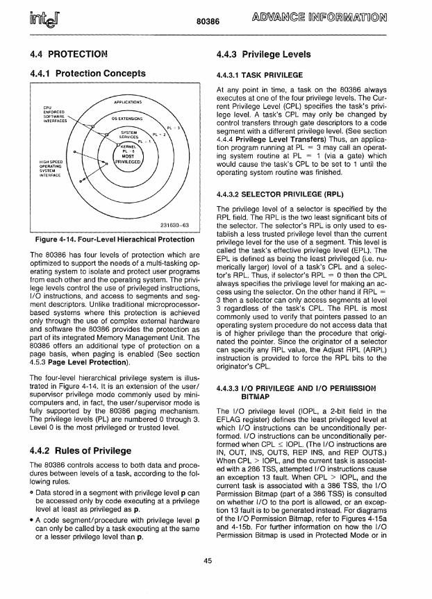
80386
4.4 PROTECTION
4.4.1 Protection Concepts
CPU ENFORCED SOFTWARE INTERFACES
HIGH SPEED OPERATING SYSTEM INTERFACE
APPLICATIONS
231630-63
Figure 4-14. Four-Level Hierachical Protection
The 80386 has four levels of protection which are optimized to support the needs of a mUlti-tasking operating system to isolate and protect user programs from each other and the operating system. The privilege levels control the use of privileged instructions, I/O instructions, and access to segments and segment descriptors. Unlike traditional microprocessorbased systems where this protection is achieved only through the use of complex external hardware and software the 80386 provides the protection as part of its integrated Memory Management Unit. The 80386 offers an additional type of protection on a page basis, when paging is enabled (See section 4.5.3 Page Level Protection).
The four-level hierarchical privilege system is illustrated in Figure 4-14. It is an extension of the user / supervisor privilege mode commonly used by minicomputers and, in fact, the user/supervisor mode is fully supported by the 80386 paging mechanism. The privilege levels (PL) are numbered 0 through 3. Level 0 is the most privileged or trusted level.
4.4.2 Rules of Privilege
The 80386 controls access to both data and procedures between levels of a task, according to the following rules.
o Data stored in a segment with privilege level p can be accessed only by code executing at a privilege level at least as privileged as p.
• A code segment/procedure with privilege level p can only be called by a task executing at the same or a lesser privilege level than p.
45
4.4.3 Privilege Levels
4.4_3.1 TASK PRIVILEGE
At any point in time, a task on the 80386 always executes at one of the four privilege levels. The Current Privilege Level (CPL) specifies the task's privilege level. A task's CPL may only be changed by control transfers through gate descriptors to a code segment with a different privilege level. (See section 4.4.4 Privilege Level Transfers) Thus, an application program running at PL = 3 may call an operating system routine at PL = 1 (via a gate) which would cause the task's CPL to be set to 1 until the operating system routine was finished.
4.4.3.2 SELECTOR PRIVILEGE (RPL)
The privilege level of a selector is specified by the RPL field. The RPL is the two least significant bits of the selector. The selector's RPL is only used to establish a less trusted privilege level than the current privilege level for the use of a segment. This level is called the task's effective privilege level (EPL). The EPL is defined as being the least privileged (i.e. numerically larger) level of a task's CPL and a selector's RPL. Thus, if selector's RPL = 0 then the CPL always specifies the privilege level for making an access using the selector. On the other hand if RPL = 3 then a selector can only access segments at level 3 regardless of the task's CPL. The RPL is most commonly used to verify that pointers passed to an operating system procedure do not access data that is of higher privilege than the procedure that originated the pointer. Since the originator of a selector can specify any RPL value, the Adjust RPL (ARPL) instruction is provided to force the RPL bits to the originator's CPL.
4.4.3_3 I/O PRIVILEGE AND 1/0 PERMISSION BITMAP
The 110 privilege level (IOPL, a 2-bit field in the EFLAG register) defines the least privileged level at which I/O instructions can be unconditionally performed. 110 instructions can be unconditionally performed when CPL s: 10PL. (The I/O instructions are IN, OUT, INS, OUTS, REP INS, and REP OUTS.) When CPL > 10PL, and the current task is associated with a 286 TSS, attempted 1/0 instructions cause an exception 13 fault. When CPL > 10PL, and the current task is associated with a 386 TSS, the I/O Permission Bitmap (part of a 386 TSS) is consulted on whether I/O to the port is allowed, or an exception 13 fault is to be generated instead. For diagrams of the 1/0 Permission Bitmap, refer to Figures 4-15a and 4-15b. For further information on how the 110 Permission Bitmap is used in Protected Mode or in
inter 80386
Virtual 8086 Mode, refer to section 4.6.4 Protection and 110 Permission Bitmap.
The 110 privilege level (IOPL) also affects whether several other instructions can be executed or cause an exception 13 fault instead. These instructions are called "IOPL·sensitive" instructions and they are CLI and STI. (Note that the LOCK prefix is not 10PL· sensitive on the 80386.)
The 10PL also affects whether the IF (interrupts en· able flag) bit can be changed by loading a value into the EFLAGS register. When CPL os: 10PL, then the IF bit can be changed by loading a new value into the EFLAGS register. When CPL > 10PL, the IF bit cannot be changed by a new value POP'ed into (or otherwise loaded into) the EFLAGS register; the IF bit merely remains unchanged and no exception is generated.
Table 4-2. Pointer Test Instructions
Instruction Operands Function
ARPL Selector, Adjust Requested Privi-Register lege Level: adjusts the
RPL of the selector to the numeric maximum of current selector RPL value and the RPL value in the register. Set zero flag if selector RPL was changed.
VERR Selector VERify for Read: sets the zero flag if the segment referred to by the selector can be read.
VERW Selector VERify for Write: sets the zero flag if the segment referred to by the selector can be written.
LSL Register, Load Segment Limit: reads Selector the segment limit into the
register if privilege rules and descriptor type allow. Set zero flag if successful.
LAR Register, Load Access Rights: reads Selector the descriptor access
rights byte into the register if privilege rules allow. Set zero flag if successful.
46
4.4.3.4 PRIVILEGE VALIDATION
The 80386 provides several instructions to speed pointer testing and help maintain system integrity by verifying that the selector value refers to an appro· priate segment. Table 4-2 summarizes the selector validation procedures available for the 80386.
This pointer verification prevents the common problem of an application at PL = 3 calling a operating systems routine at PL = 0 and passing the operating system routine a "bad" pointer which corrupts a data structure belonging to the operating system. If the operating system routine uses the ARPL instruction to ensure that the RPL of the selector has no greater privilege than that of the caller, then this problem can be avoided.
4.4.3.5 DESCRIPTOR ACCESS
There are basically two types of segment accesses: those involving code segments such as control transfers, and those involving data accesses. Deter· mining the ability of a task to access a segment involves the type of segment to be accessed, the instruction used, the type of descriptor used and CPL, RPL, and DPL as described above.
Any time an instruction loads data segment registers (DS, ES, FS, GS) the 80386 makes protection validation checks. Selectors loaded in the DS, ES, FS, GS registers must refer only to data segments or readable code segments. The data access rules are specified in section 4.2.2 Rules of Privilege. The only exception to those rules is readable conforming code segments which can be accessed at any privilege level.
Finally the privilege validation checks are performed. The CPL is compared to the EPL and if the EPL is more privileged than the CPL an exception 13 (general protection fault) is generated.
The rules regarding the stack segment are slightly different than those involving data segments. Instructions that load selectors into SS must refer to data segment descriptors for writeable data segments. The DPL and RPL must equal the CPL. All other descriptor types or a privilege level violation will cause exception 13. A stack not present fault causes exception 12. Note that an exception 11 is used for a not-present code or data segment.
4.4.4 Privilege Level Transfers
Inter-segment control transfers occur when a selector is loaded in the CS register. For a typical system most of these transfers are simply the result of a call
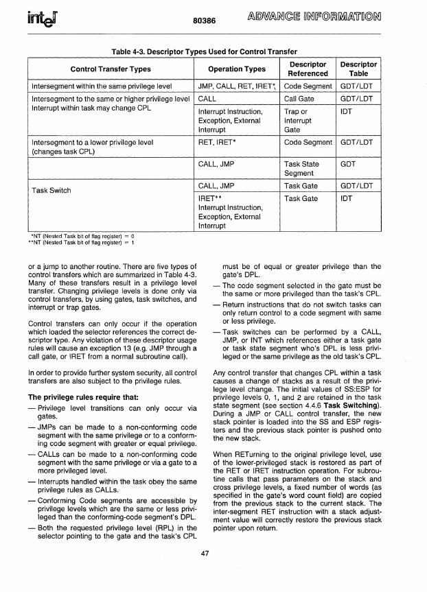
80386
Table 4-3. Descriptor Types Used for Control Transfer
Control Transfer Types
Intersegment within the same privilege level
Intersegment to the same or higher privilege level Interrupt within task may change CPL
Intersegment to a lower privilege level (changes task CPL)
Task Switch
'NT (Nested Task bit of flag register) ~ 0 "NT (Nested Task bit of flag register) ~ 1
or a jump to another routine. There are five types of control transfers which are summarized in Table 4-3. Many of these transfers result in a privilege level transfer. Changing privilege levels is done only via control transfers, by using gates, task switches, and interrupt or trap gates.
Control transfers can only occur if the operation which loaded the selector references the correct descriptor type. Any violation of these descriptor usage rules will cause an exception 13 (e.g. JMP through a call gate, or IRET from a normal subroutine call).
In order to provide further system security, all control transfers are also subject to the privilege rules.
The privilege rules require that:
- Privilege level transitions can only occur via gates.
- JMPs can be made to a non-conforming code segment with the same privilege or to a conforming code segment with greater or equal privilege.
- CALLs can be made to a non-conforming code segment with the same privilege or via a gate to a more privileged level.
- Interrupts handled within the task obey the same privilege rules as CALLs.
- Conforming Code segments are accessible by privilege levels which are the same or less privileged than the conforming-code segment's OPL.
- Both the requested privilege level (RPL) in the selector pOinting to the gate and the task's CPL
Operation Types Descriptor Descriptor
Referenced Table
JMP, CALL, RET, IRET', Code Segment GOT/LOT
CALL Call Gate GOT/LOT
Interrupt Instruction, Trap or lOT Exception, External Interrupt Interrupt Gate
RET,IRET' Code Segment GOT/LOT
CALL, JMP Task State GOT Segment
CALL, JMP Task Gate GOT/LOT
IRET" Task Gate lOT Interrupt Instruction, Exception, External Interrupt
47
must be of equal or greater privilege than the gate's OPL.
- The code segment selected in the gate must be the same or more privileged than the task's CPL.
- Return instructions that do not switch tasks can only return control to a code segment with same or less privilege.
- Task switches can be performed by a CALL, JMP, or INT which references either a task gate or task state segment who's OPL is less privileged or the same privilege as the old task's CPL.
Any control transfer that changes CPL within a task causes a change of stacks as a result of the privilege level change. The initial values of SS:ESP for privilege levels 0, 1, and 2 are retained in the task state segment (see section 4.4.6 Task Switching). During a JMP or CALL control transfer, the new stack pointer is loaded into the SS and ESP registers and the previous stack pointer is pushed onto the new stack.
When RETurning to the original privilege level, use of the lower-privileged stack is restored as part of the RET or IRET instruction operation. For subroutine calls that pass parameters on the stack and cross privilege levels, a fixed number of words (as specified in the gate's word count field) are copied from the previous stack to the current stack. The inter-segment RET instruction with a stack adjustment value will correctly restore the previous stack pointer upon return.

p-------------. , ACCESS I TSS
, , f+ -, RIGHTS LIMIT , , , , , ,
BASE f+ , , , , : 31 PROGRAM 0' , , INVISIBLE , 10 ______ ------_.
TASK REGISTER
TR SELECTOR ~ 15 0
Type ~ 9: Available 386 TSS, Type ~ B. Busy 386 TSS
31
80386
31 16
0000000000000000 I ESPO
0000000000000000 I ESPI
15
BACK LINK
SSO
\~ 4
8
C
10
TSS BASE
STACKS FOR
0000000000000000 I SSI CPL 0,1,2
ESP2
0000000000000000 I CR3
EIP
EFLAGS
EAX
ECX
EDX
EBX
ESP
EBP
ESI
EDI
0000000000000000
0000000000000000
0000000000000000
0000000000000000
0000000000000000
0000000000000000
0000000000000000
SS2
ES
CS
SS
OS
FS
GS
LOT
14
18
lC
20
24
28
2C
30
34
38
3C
40
44
48
4C
50
54
58
5C
60
CURRENT TASK STATE
BILMAP _OFFSET(15:0} 0000000000000000
I'~ AVAILABLE ----h SYSTEM STATUS, ETC. r- IN 386 TSS
31 24 23 16 15 8
63 56 55 48 47 40
95 88 87 80 79 72
h
r- I/o PERMISSION BITMAP
65407 (ONE BIT PER BYTE I/O PORT. BITMAP MAY BE 65439
TRUNCATED USING TSS LIMIT.) 65471 I 65503 I 65535 I
7
39
71
0
OEBUG TRAP BIT
32 1'a'LM
64
96
h
65472
65504
"FFH"
OFFSE T + C
T + 10 OFFSE
OFFSE T + lFEC
T + lFFO
T + 1 FF4
ET+ lFF8
T + lFFC
OFFSE
OFFSE
OFFS
OFFSE
OFFSE T + 2000
t TSS LlMIT=OF FSET + 2000H
386 TSS DESCRIPTOR (IN GOT) 0
SEGMENT BASE 15 ••• 0 SEGMENT LIMIT 15 •. 0
BASE 31..24 H 1 101 0 11L~~~~ P I D~L 10 1 I TYjE I I BASE
23 .• 16 231630-64
Figure 4-15a. 386 TSS and TSS Registers
48
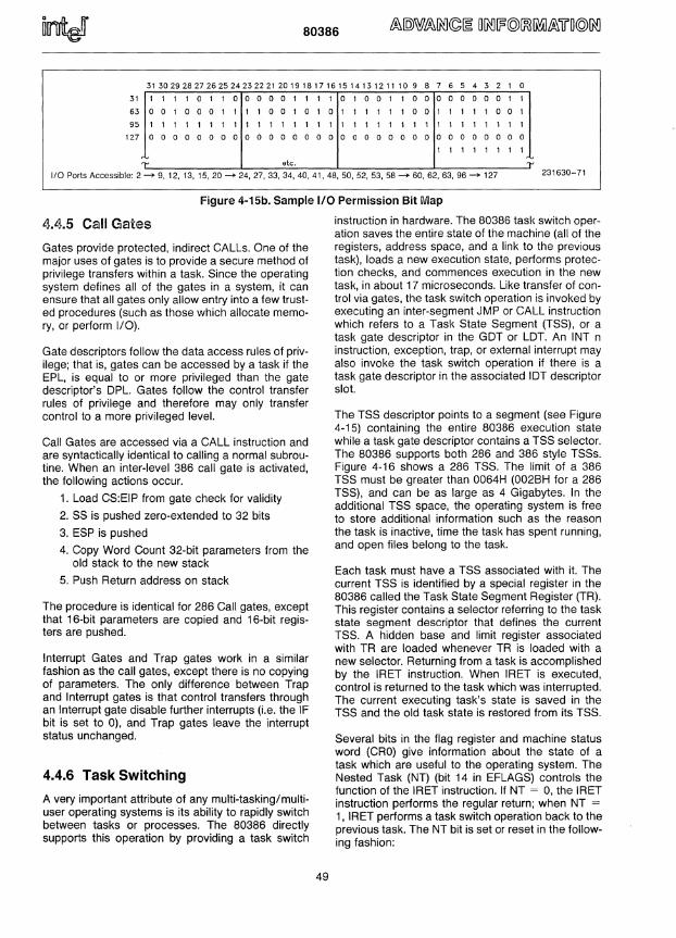
80386
31
63
95
127
31302928272625242322212019181716151413121110987654321 0
1 1 1 1 0 1 1 0 o 0 0 0 1 1 1 1 0 1 0 0 1 1 0 0 o 0 0 0 0 0 1 1
0 0 1 0 0 0 1 1 1 1 0 0 1 0 1 0 1 1 1 1 1 1 0 0 1 1 1 1 1 o 0 1
1 1 1 1 1 1 1 1 1 1 1 1 1 1 1 1 1 1 1 1 1 1 1 1 1 1 1 1 1 1 1 1
0 0 0 0 0 0 0 000 o 0 0 0 0 o 0 0 0 0 0 0 0 0 0 0 0 0 0 o 0 0
1 1 1 1 1 1 1 1
'l' etc. 'l'
1/0 Ports Accessible: 2 ---> 9, 12, 13, 15, 20 ---> 24, 27, 33, 34, 40, 41, 48, 50, 52, 53, 58 ---> 60, 62, 63, 96 ---> 127 231630-71
Figure 4-15b. Sample I/O Permission Bit Map
4.4.5 Call Ga~es
Gates provide protected, indirect CALLs. One of the major uses of gates is to provide a secure method of privilege transfers within a task. Since the operating system defines all of the gates in a system, it can ensure that all gates only allow entry into a few trusted procedures (such as those which allocate memory, or perform I/O).
Gate descriptors follow the data access rules of privilege; that is, gates can be accessed by a task if the EPL, is equal to or more privileged than the gate descriptor's OPL. Gates follow the control transfer rules of privilege and therefore may only transfer control to a more privileged level.
Call Gates are accessed via a CALL instruction and are syntactically identical to calling a normal subroutine. When an inter-level 386 call gate is activated, the following actions occur.
1. Load CS:EIP from gate check for validity
2. SS is pushed zero-extended to 32 bits
3. ESP is pushed
4. Copy Word Count 32-bit parameters from the old stack to the new stack
5. Push Return address on stack
The procedure is identical for 286 Call gates, except that 16-bit parameters are copied and 16-bit registers are pushed.
Interrupt Gates and Trap gates work in a similar fashion as the call gates, except there is no copying of parameters. The only difference between Trap and Interrupt gates is that control transfers through an Interrupt gate disable further interrupts (i.e. the IF bit is set to 0), and Trap gates leave the interrupt status unchanged.
4.4.6 Task Switching
A very important attribute of any multi-tasking/multiuser operating systems is its ability to rapidly switch between tasks or processes. The 80386 directly supports this operation by providing a task switch
49
instruction in hardware. The 80386 task switch operation saves the entire state of the machine (all of the registers, address space, and a link to the previous task), loads a new execution state, performs protection checks, and commences execution in the new task, in about 17 microseconds. Like transfer of control via gates, the task switch operation is invoked by executing an inter-segment JMP or CALL instruction which refers to a Task State Segment (TSS), or a task gate descriptor in the GOT or LOT. An INT n instruction, exception, trap, or external interrupt may also invoke the task switch operation if there is a task gate descriptor in the associated lOT descriptor slot.
The TSS descriptor points to a segment (see Figure 4-1 5) containing the entire 80386 execution state while a task gate descriptor contains a TSS selector. The 80386 supports both 286 and 386 style TSSs. Figure 4-16 shows a 286 TSS. The limit of a 386 TSS must be greater than 0064H (002BH for a 286 TSS), and can be as large as 4 Gigabytes. In the additional TSS space, the operating system is free to store additional information such as the reason the task is inactive, time the task has spent running, and open files belong to the task.
Each task must have a TSS associated with it. The current TSS is identified by a special register in the 80386 called the Task State Segment Register (TR). This register contains a selector referring to the task state segment descriptor that defines the current TSS. A hidden base and limit register associated with TR are loaded whenever TR is loaded with a new selector. Returning from a task is accomplished by the IRET instruction. When IRET is executed, control is returned to the task which was interrupted. The current executing task's state is saved in the TSS and the old task state is restored from its TSS.
Several bits in the flag register and machine status word (CRO) give information about the state of a task which are useful to the operating system. The Nested Task (NT) (bit 14 in EFLAGS) controls the function of the IRET instruction. If NT = 0, the IRET instruction performs the regular return; when NT =
1, IRET performs a task switch operation back to the previous task. The NT bit is set or reset in the following fashion:

infef 80386
15 0
BACK LINK SELECTOR TO TSS
SP FOR CPL 0
SS FOR CPL 0
SP FOR CPL 1
SS FOR CPL 1
SP FOR CPL 2
SS FOR CPL 2
IP (ENTRY POINT)
FLAGS
AX
CX
OX
BX
SP
BP
SI
01
ES SELECTOR
CS SELECTOR
SS SELECTOR
OS SELECTOR
TASK'S LOT SELECTOR
AVAILABLE ,
o 2
4
6 INITIAL STACKS
8 FOR CPL 0,1,2
A
C
E
10
12
14
16
18 CURRENT
1A TASK
IC STATE
IE
20
22
24
26
28
2A
231630-65
Figure 4·16. 286 TSS
When a GALL or INT instruction initiates a task switch, the new TSS will be marked busy and the back link field of the new TSS set to the old TSS selector. The NT bit of the new task is set by GALL or INT initiated task switches. An interrupt that does not cause a task switch will clear NT. (The NT bit will be restored after execution of the interrupt handler) NT may also be set or cleared by POPF or IRET instructions.
The 386 task state segment is marked busy by changing the descriptor type field from TYPE 9H to TYPE BH. A 286 TSS is marked busy by changing the descriptor type field from TYPE 1 to TYPE 3. Use of a selector that references a busy task state segment causes an exception 13.
The Virtual Mode (VM) bit 17 is used to indicate if a task, is a virtual 8086 task. If VM = 1, then the tasks will use the Real Mode addressing mechanism. The virtual 8086 environment is only entered and exited via a task switch (see section 4.6 Virtual Mode).
The coprocessor's state is not automatically saved when a task switch occurs, because the incoming
50
task may not use the coprocessor. The Task Switched (TS) Bit (bit 3 in the GRO) helps deal with the coprocessor's state in a multi-tasking environment. Whenever the 80386 switches tasks, it sets the TS bit. The 80386 detects the first use of a processor extension instruction after a task switch and causes the processor extension not available exception 7. The exception handler for exception 7 may then decide whether to save the state of the coprocessor. A processor extension not present exception (7) will occur when attempting to execute an ESG or WAIT instruction if the Task Switched and Monitor coprocessor extension bits are both set (i.e. TS = 1 and MP = 1).
The T bit in the 386 TSS indicates that the processor should generate a debug exception when switching to a task. If T = 1 then upon entry to a new task a debug exception 1 will be generated.
4.4.7 Initialization and Transition to Protected Mode
Since the 80386 begins executing in Real Mode immediately after RESET it is necessary to initialize the system tables and registers with the appropriate values.
The GOT and lOT registers must refer to a valid GOT and lOT. The lOT should be at least 256 bytes long, and GOT must contain descriptors for the initial code, and data segments. Figure 4-17 shows the tables and Figure 4-18 the descriptors needed for a simple Protected Mode 80386 system. It has a single code and single data/stack segment each four gigabytes long and a single privilege level PL = O.
The actual method of enabling Protected Mode is to load GRO with the PE bit set, via the MOV GRO, R/M instruction. This puts the 80386 in Protected Mode.
After enabling Protected Mode, the next instruction should execute an intersegment JMP to load the GS register and flush the instruction decode queue. The final step is to load all of the data segment registers with the initial selector values.
An alternate approach to entering Protected Mode which is especially appropriate for multi-tasking operating systems, is to use the built in task-switch to load all of the registers. In this case the GOT would contain two TSS descriptors in addition to the code and data descriptors needed for the first task. The first JMP instruction in Protected Mode would jump to the TSS causing a task switch and loading all of the registers with the values stored in the TSS. The Task State Segment Register should be initialized to point to a valid TSS descriptor since a task switch saves the state of the current task in a task state segment.
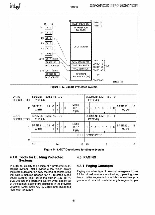
80386
31 a FFFFFFFF 15 a RESET ROUTINES
SS §ITI tFtFtFto INITIALIZATION
GS §ITI ROUTINES
FS §ITI ES §ITI
USER MEMORY
CS
GDTR
"""'" 1 DATA DESCRIPTOR 00000110
CODE DESCRIPTOR 00000 108 GDT
NULL SELECTOR 00000100
INTERRUPT t DESCRIPTORS (32)
IDT t
00000000 231630-66
Figure 4-17. Simple Protected System
DATA DESCRIPTOR
2
CODE DESCRIPTOR
o
SEGMENT BASE 15 ... 0 0118 (H)
BASE 31 ... 24 G o 0 00 (H) 1
0 1
SEGMENT BASE 15 ... 0 0118 (H)
BASE 31 ... 24 G 0 00 (H) 1 1
o 0
31 24
SEGMENT LIMIT 15 ... 0 FFFF (H)
LIMIT o BASE 23 ... 16 19.16 1 001 o 0 1 F(H)
00 (H)
SEGMENT LIMIT 15 ... 0 FFFF (H)
LIMIT BASE 23 ... 16
19.16 1 001 1 o 1 0 00 (H)
F(H)
NULL DESCRIPTOR
16 15 8 o
Figure 4-18. GOT Descriptors for Simple System
4.4.8 Tools for Building Protected Systems
In order to simplify the design of a protected multi· tasking system, Intel provides a tool which allows the system designer an easy method of constructing the data structures needed for a Protected Mode 80386 system. This tool is the builder BLD·386TM. BLD·386 lets the operating system writer specify all of the segment descriptors discussed in the previous sections (LOTs, lOTs, GDTs, Gates, and TSSs) in a high·level language.
51
4.5 PAGING
4.5.1 Paging Concepts
Paging is another type of memory management use· ful for virtual memory multitasking operating systems. Unlike segmentation which modularizes programs and data into variable length segments, pa-
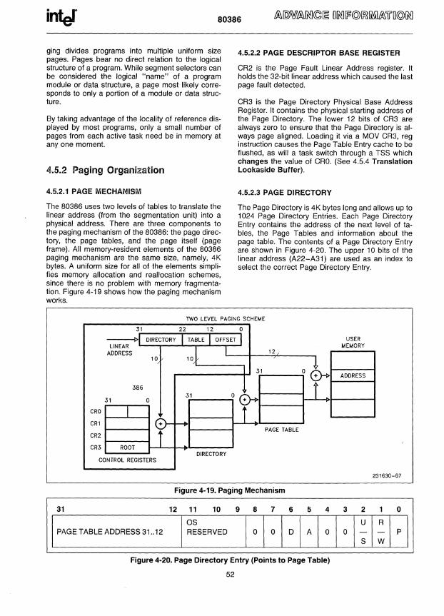
inter 80386
ging divides programs into multiple uniform size pages. Pages bear no direct relation to the logical structure of a program. While segment selectors can be considered the logical "name" of a program module or data structure, a page most likely corresponds to only a portion of a module or data structure.
By taking advantage of the locality of reference displayed by most programs, only a small number of pages from each active task need be in memory at anyone moment.
4.5.2 Paging Organization
4.5.2.1 PAGE MECHANISM
The 80386 uses two levels of tables to translate the linear address (from the segmentation unit) into a physical address. There are three components to the paging mechanism of the 80386: the page directory, the page tables, and the page itself (page frame). All memory-resident elements of the 80386 paging mechanism are the same size, namely, 4K bytes. A uniform size for all of the elements simplifies memory allocation and reallocation schemes, since there is no problem with memory fragmentation. Figure 4-19 shows how the paging mechanism works.
4.5.2.2 PAGE DESCRIPTOR BASE REGISTER
CR2 is the Page Fault Linear Address register. It holds the 32-bit linear address which caused the last page fault detected.
CR3 is the Page Directory Physical Base Address Register. It contains the physical starting address of the Page Directory. The lower 12 bits of CR3 are always zero to ensure that the Page Directory is always page aligned. Loading it via a MOV CR3, reg instruction causes the Page Table Entry cache to be flushed, as will a task switch through a TSS which changes the value of CRO. (See 4.5.4 Translation Lool<aside Buffer).
4.5.2.3 PAGE DIRECTORY
The Page Directory is 4K bytes long and allows up to 1024 Page Directory Entries. Each Page Directory Entry contains the address of the next level of tables, the Page Tables and information about the page table. The contents of a Page Directory Entry are shown in Figure 4-20. The upper 10 bits of the linear address (A22-A31) are used as an index to select the correct Page Directory Entry.
TWO LEVEL PAGING SCHEME
31 22 12 0
~ DIRECTORY I TABLE I OFFSET I LINEAR
ADDRESS 10}
l 12 10
'1: 31
386 31 'r 31 0
CRO I
f ~ CR1 PAGE TABLE
CR2
CR3 ROOT DIRECTORY
CONTROL REGISTERS
Figure 4-19. Paging Mechanism
31 12 11 10 9 8 7 6 5 4
OS PAGE TABLE ADDRESS 31 .. 12 RESERVED 0 0 D A 0
Figure 4-20. Page Directory Entry (POints to Page Table)
52
USER MEMORY
ADDRESS
231630-67
3 2 1 0
U R 0 - - P
S W

80386
31 12 11 10 9 8 7 6 5 4 3 2 1 0
OS U R PAGE FRAME ADDRESS 31 .. 12 RESERVED 0 0 D A 0 0 - - P
S W
Figure 4-21. Page Table Entry (Points to Page)
4.5.2.4 PAGE TABLES
Each Page Table is 4K bytes and holds up to 1024 Page Table Entries. Page Table Entries contain the starting address of the page frame and statistical information about the page (see Figure 4-21). Address bits A12-A21 are used as an index to select one of the 1024 Page Table Entries. The 20 upperbit page frame address is concatenated with the lower 12 bits of the linear address to form the physical address. Page tables can be shared between tasks and swapped to disks.
4.5.2.5 PAGE DIRECTORY/TABLE ENTRIES
The lower 12 bits of the Page Table Entries and Page Directory Entries contain statistical information about pages and page tables respectively. The P (Present) bit 0 indicates if a Page Directory or Page Table entry can be used in address translation. If P = 1 the entry can be used for address translation if P= 0 the entry can not be used for translation, and all of the other bits are available for use by the software. For example the remaining 31 bits could be used to indicate where on the disk the page is stored.
The A (Accessed) bit 5, is set by the 80386 for both types of entries before a read or write access occurs to an address covered by the entry. The D (Dirty) bit 6 is set to 1 before a write to an address covered by that page table entry occurs. The D bit is undefined for Page Directory Entries. When the P, A and D bits are updated by the 80386, the processor generates a Read-Modify-Write cycle which locks the bus and prevents conflicts with other processors or perpherials. Software which modifies these bits should use the LOCK prefix to ensure the integrity of the page tables in multi-master systems.
The 3 bits marked OS Reserved in Figure 4-20 and Figure 4-21 (bits 9-11) are software definable. OSs are free to use these bits for whatever purpose they wish. An example use of the OS Reserved bits would be to store information about page aging. By keeping track of how long a page has been in memory since being accessed, an operating system can implement a page replacement algorithm like Least Recently Used.
The (User/Supervisor) U/S bit 2 and the (Read/ Write) R/W bit 1 are used to provide protection attributes for individual pages.
53
4.5.3 Page Level Protection (R/W, U/S Bits)
The 80386 provides a set of protection attributes for paging systems. The paging mechanism distinguishes between two levels of protection: User which corresponds to level 3 of the segmentation based protection, and supervisor which encompasses all of the other protection levels (0, 1, 2). Programs executing at Level 0, 1 or 2 bypass the page protection, although segmentation based protection is still enforced by the hardware.
The U/S and R/W bits are used to provide User/Supervisor and Read/Write protection for individual pages or for all pages covered by a Page Table Directory Entry. The U/S and R/W bits in the first level Page Directory Table apply to all pages described by the page table pointed to by that directory entry. The U/S and R/W bits in the second level Page Table Entry apply only to the page described by that entry. The U/S and R/W bits for a given page are obtained by taking the most restrictive of the U/S and R/W from the Page Directory Table Entries and the Page Table Entries and using these bits to address the page.
Example: If the U/S and R/W bits for the Page Directory entry were 10 and the U/S and R/W bits for the Page Table Entry were 01, the access rights for the page would be 01, the numerically smaller of the two. Table 4-4 shows the affect of the U/S and R/W bits on accessing memory.
Table 4-4. Protection Provided by R/W and U/S
U/S R/W Permitted Permitted Access
Level 3 Levels 0, 1, or 2
0 0 None Read/Write 0 1 None Read/Write 1 0 Read-Only Read/Write 1 1 Read/Write Read/Write
However a given segment can be easily made readonly for level 0, 1, or 2 via the use of segmented protection mechanisms. (Section 4.4 Protection).
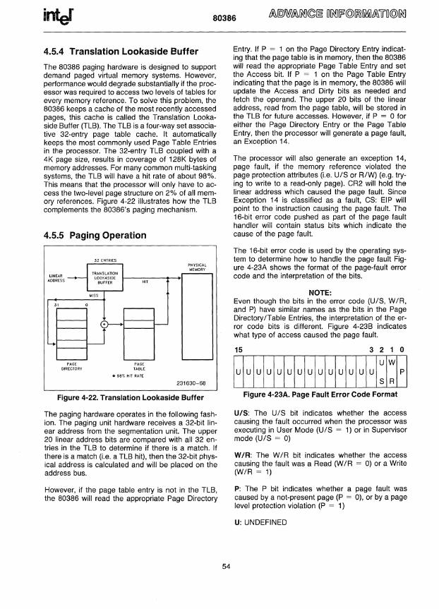
80386
4.5.4 Translation Lookaside Buffer
The 80386 paging hardware is designed to support demand paged virtual memory systems. However, performance would degrade substantially if the processor was required to access two levels of tables for every memory reference. To solve this problem, the 80386 keeps a cache of the most recently accessed pages, this cache is called the Translation Lookaside Buffer (TLB). The TLB is a four-way set associative 32-entry page table cache. It automatically keeps the most commonly used Page Table Entries in the processor. The 32-entry TLB coupled with a 4K page size, results in coverage of 128K bytes of memory addresses. For many common multi-tasking systems, the TLB will have a hit rate of about 98%. This means that the processor will only have to access the two-level page structure on 2% of all memory references. Figure 4-22 illustrates how the TLB complements the 80386's paging mechanism.
4.5.5 Paging Operation
32 ENTRIES PHYSICAL ~EMORY
TRANSLATION
A~~~~~S --+- LODKASIOE BUFFER HIT
MISS
31 0
U t--
4
PAGE PAGE DIRECTORY TABLE
098% HIT RATE
231630-68
Figure 4-22. Translation Lookaside Buffer
The paging hardware operates in the following fash· ion. The paging unit hardware receives a 32-bit linear address from the segmentation unit. The upper 20 linear address bits are compared with all 32 entries in the TLB to determine if there is a match. If there is a match (Le. a TLB hit), then the 32-bit phys· ical address is calculated and will be placed on the address bus.
However, if the page table entry is not in the TLB, the 80386 will read the appropriate Page Directory
54
Entry. If P = 1 on the Page Directory Entry indicating that the page table is in memory, then the 80386 will read the appropriate Page Table Entry and set the Access bit. If P = 1 on the Page Table Entry indicating that the page is in memory, the 80386 will update the Access and Dirty bits as needed and fetch the operand. The upper 20 bits of the linear address, read from the page table, will be stored in the TLB for future accesses. However, if P = 0 for either the Page Directory Entry or the Page Table Entry, then the processor will generate a page fault, an Exception 14.
The processor will also generate an exception 14, page fault, if the memory reference violated the page protection attributes (Le. U/S or R/W) (e.g. trying to write to a read-only page). CR2 will hold the linear address which caused the page fault. Since Exception 14 is classified as a fault, CS: EIP will point to the instruction causing the page fault. The 16-bit error code pushed as part of the page fault handler will contain status bits which indicate the cause of the page fault.
The 16-bit error code is used by the operating system to determine how to handle the page fault Figure 4-23A shows the format of the page-fault error code and the interpretation of the bits.
NOTE: Even though the bits in the error code (U/S, W/R, and P) have similar names as the bits in the Page Directory/Table Entries, the interpretation of the error code bits is different. Figure 4-23B indicates what type of access caused the page fault.
15 3 2 1 0
lulululululululululululululul~I:lpl Figure 4-23A. Page Fault Error Code Format
U/S: The UlS bit indicates whether the access causing the fault occurred when the processor was executing in User Mode (U/S = 1) or in Supervisor mode (U/S = 0)
W/R: The W/R bit indicates whether the access causing the fault was a Read (W/R = 0) or a Write (W/R = 1)
P: The P bit indicates whether a page fault was caused by a not-present page (P = 0), or by a page level protection violation (P = 1)
U: UNDEFINED
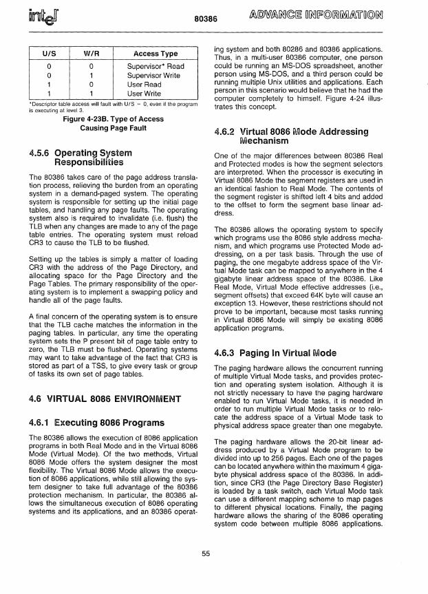
80386
U/S W/R Access Type
0 0 Supervisor' Read 0 1 Supervisor Write 1 0 User Read 1 1 User Write
'Descriptor table access will fault with u/s 0, even lithe program is executing at level 3.
Figure 4-238. Type of Access Causing Page Fault
4.5.6 Operating System Responsibilities
The 80386 takes care of the page address translation process, relieving the burden from an operating system in a demand-paged system. The operating system is responsible for setting up the initial page tables, and handling any page faults. The operating system also is required to invalidate (i.e. flush) the TLB when any changes are made tD any of the page table entries. The operating system must reload CR3 to cause the TLB to be flushed.
Setting up the tables is simply a matter of loading CR3 with the address of the Page Directory, and allocating space for the Page Directory and the Page Tables. The primary responsibility of th~ operating system is to implement a swapping policy and handle all of the page faults.
A final concern of the operating system is to ensure that the TLB cache matches the information in the paging tables. In particular, any time the operating system sets the P present bit of page table entry to zero, the TLB must be flushed. Operating systems may want to take advantage of the fact that CR3 is stored as part of a TSS, to give every task or group of tasks its own set of page tables.
4.6 VIRTUAL 8086 ENVIRONMENT
4.6.1 Executing 8086 Programs
The 80386 allows the execution of 8086 application programs in both Real Mode and in the Virtual 8086 Mode (Virtual Mode). Of the two methods, Virtual 8086 Mode offers the system designer the most flexibility. The Virtual 8086 Mode allows the execution of 8086 applications, while still allowing the system designer to take full advantage of the 80386 protection mechanism. In particular, the 80386 allows the simultaneous execution of 8086 operating systems and its applications, and an 80386 ope rat-
55
ing system and both 80286 and 80386 applications. Thus, in a multi-user 80386 computer, one person could be running an MS-DOS spreadsheet, another person using MS-DOS, and a third person could be running multiple Unix utilities and applications. Each person in this scenario would believe that he had the computer completely to himself. Figure 4-24 Illustrates this concept.
4.6.2 Virtual 8086 Mode Addressing Mechanism
One of the major differences between 80386 Real and Protected modes is how the segment selectors are interpreted. When the processor is executing in Virtual 8086 Mode the segment registers are used in an identical fashion to Real Mode. The contents of the segment register is shifted left 4 bits and added to the offset to form the segment base linear address.
The 80386 allows the operating system to specify which programs use the 8086 style address mechanism, and which programs use Protected Mode addressing, on a per task basis. Through the use of paging, the one megabyte address space of the Virtual Mode task can be mapped to anywhere in the 4 gigabyte linear address space ?f the 80386. Like Real Mode, Virtual Mode effeclive addresses (I.e., segment offsets) that exceed 64K byte will cause an exception 13. However, these restrictions should ~ot prove to be important, because most tasks running in Virtual 8086 Mode will simply be existing 8086 application programs.
4.6.3 Paging In Virtual Mode
The paging hardware allows the concurrent running of multiple Virtual Mode tasks, and provides protection and operating system isolation. Although it is not strictly necessary to have the paging hardware enabled to run Virtual Mode tasks, it is needed In order to run multiple Virtual Mode tasks or to relocate the address space of a Virtual Mode task to physical address space greater than one megabyte.
The paging hardware allows the 20-bit linear address produced by a Virtual Mode program to be divided into up to 256 pages. Each one of the pages can be located anywhere within the maximum 4 gigabyte physical address space of the 80386. In ~ddition, since CR3 (the Page Directory Base Register) is loaded by a task switch, each Virtual Mode task can use a different mapping scheme to map pages to different physical locations. Finally, the paging hardware allows the sharing of the 8086 operating system code between multiple 8086 applications.
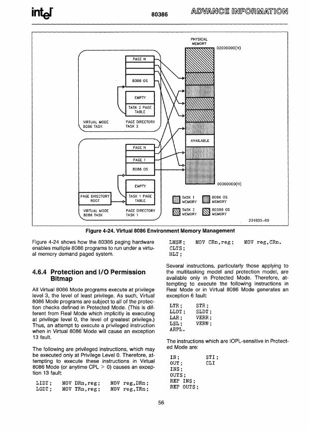
inter 80386
VIRTUAL MODE 8086 TASK
PAGE DIRECTORY ROOT
VIRTUAL MODE 8086 TASK
8086 OS
EMPTY
TASK 1 PAGE TABLE
PAGE DIRECTORY TASK 1
PHYSICAL MEMORY
........... ~~~ 02000000(H)
~I TASK 1 WI!! MEMORY
I777l TASK 2 rtfLA MEMORY
OOOOOOOO(H)
111 8086 OS MEMORY
~ 80386 OS ~ MEMORY
231630-69
Figure 4-24. Virtual 8086 Environment Memory Management
Figure 4·24 shows how the 80386 paging hardware enables multiple 8086 programs to run under a virtu· al memory demand paged system.
4.6.4 Protection and 1/0 Permission Bitmap
All Virtual 8086 Mode programs execute at privilege level 3, the level of least privilege. As such, Virtual 8086 Mode programs are subject to all of the protection checks defined in Protected Mode. (This is different from Real Mode which implicitly is executing at privilege level 0, the level of greatest privilege.) Thus, an attempt to execute a privileged instruction when in Virtual 8086 Mode will cause an exception 13 fault.
The following are privileged instructions, which may be executed only at Privilege Level o. Therefore, attempting to execute these instructions in Virtual 8086 Mode (or anytime CPL > 0) causes an exception 13 fault:
LIDT: MOV DRn,reg: MOV reg,DRn: LGDT: MOV TRn,reg: MOV reg,TRn:
56
LMSW: CLTS; HLT:
MOV CRn,reg: MOV reg,CRn.
Several instructions, particularly those applying to the multitasking model and protection model, are available only in Protected Mode. Therefore, attempting to execute the following instructions in Real Mode or in Virtual 8086 Mode generates an exception 6 fault:
LTR; LLDT; LAR: LSL; ARPL.
STR; SLDT; VERR: VERW;
The instructions which are IOPL-sensitive in Protected Mode are:
IN; STI: OUT; CLI INS: OUTS; REP INS; REP OUTS;
80386
In Virtual 8086 Mode, a slightly different set of instructions are made 10PL-sensitive. The following instructions are 10PL-sensitive in Virtual 8086 Mode:
INT n; STI; PUSHF; eLI; POPF; IRET
The PUSHF, POPF, and IRET instructions are 10PLsensitive in Virtual 8086 Mode only. This provision allows the IF flag (interrupt enable flag) to be virtualized to the Virtual 8086 Mode program. The INT n software interrupt instruction is also 10PL-sensitive in Virtual 8086 Mode. Note, however, that the INT 3 (opcode OCCH), INTO, and BOUND instructions are not 10PL-sensitive in Virtual 8086 mode (they aren't 10PL sensitive in Protected Mode either).
Note that the I/O instructions (IN, OUT, INS, OUTS, REP INS, and REP OUTS) are not 10PL-sensitive in Virtual 8086 mode. Rather, the I/O instructions become automatically sensitive to the I/O Permission Bitmap contained in the 386 Task State Segment. The I/O Permission Bitmap, automatically used by the 80386 in Virtual 8086 Mode, is illustrated by Figures 4.15a and 4-15b.
The I/O Permission Bitmap can be viewed as a 0-64 Kbit bit string, which begins in memory at offset BiLMap_Offset in the current TSS. the 16-bit pointer BiLMap_Offset (15:0) is found in the word beginning at offset 66H (102 decimal) from the TSS base, as shown in Figure 4-15a.
Each bit in the I/O Permission Bitmap corresponds to a single byte-wide I/O port, as illustrated in Figure 4-15a. If a bit is 0, I/O to the corresponding bytewide port can occur without generating an exception. Otherwise the I/O instruction causes an exception 13 fault. Since every byte-wide I/O port must be protectable, all bits corresponding to a word-wide or dword-wide port must be a for the word-wide or dword-wide I/O to.be permitted. If all the referenced bits are 0, the I/O will be allowed. If any referenced bits are 1, the attempted I/O will cause an exception 13 fault.
Due to the use of a pointer to the base of the I/O Permission Bitmap, the bitmap may be located anywhere within the TSS, or may be ignored completely by pointing the BiLMap_Offset (15:0) beyond the limit of the TSS segment. In the same manner, only a small portion of the 64K I/O space need have an associated map bit, by adjusting the TSS limit to truncate the bitmap. This eliminates the commitment of 8K of memory when a complete bitmap is not required, while allowing the fully general case if desired.
57
EXAMPLE OF BITMAP FOR I/O PORTS 0-255: Setting the TSS limit to {biLMap_Offset + 31 + 1"l [0' see note below] will allow a 32-byte bitmap for the I/O ports #0-255, plus a terminator byte of all 1 's [" see note below]. This allows the I/O bitmap to control I/O Permission to I/O port 0-255 while causing an exception 13 fault on attempted I/O to any I/O port 256 through 65,565.
"IMPORTANT IMPLEMENTATION NOTE: Beyond the last byte of I/O mapping information in the I/O Permission Bitmap must be a byte containing all 1 'so The byte of all 1 's must be within the limit of the 386 TSS segment (see Figure 4-15a).
4.6.5 Interrupt Handling
In order to fully support the emulation of an 8086 machine, interrupts in Virtual 8086 Mode are handled in a unique fashion. When running in Virtual Mode all interrupts and exceptions involve a privilege change back to the host 80386 operating system. The 80386 operating system determines if the interrupt comes from a Protected Mode application or from a Virtual Mode program by examining the VM bit in the EFLAGS image stored on the stack.
When a Virtual Mode program is interrupted and execution passes to the interrupt routine at level 0, the VM bit is cleared. However, the VM bit is still set in the EFLAG image on the stack.
The 80386 operating system in turn handles the exception or interrupt and then returns control to the 8086 program. The 80386 operating system may choose to let the 8086 operating system handle the interrupt or it may emulate the function of the interrupt handler. For example, many 8086 operating system calls are accessed by PUSHing parameters on the stack, and then executing an INT n instruction. If the 10PL is set to a then all INT n instructions will be intercepted by the 80386 operating system. The 80386 operating system could emulate the 8086 operating system's call. Figure 4-25 shows how the 80386 operating system could intercept an 8086 operating system's call to "Open a File".
An 80386 operating system can provide a Virtual 8086 Environment which is totally transparent to the application software via intercepting and then emulating 8086 operating system's calls, and intercepting IN and OUT instructions.
4.6.6 Entering and Leaving Virtual 8086 Mode
Virtual 8086 mode is entered by executing an IRET instruction (at CPL=O), or Task Switch (at any CPL) to a 386 task whose 386 TSS has a FLAGS image containing a 1 in the VM bit position while the proc-

intJ 80386
essor is executing in Protected Mode. That is, one way to enter Virtual 8086 mode is to switch to a task with a 386 TSS that has a 1 in the VM bit in the EFLAGS image. The other way is to execute a 32-bit IRET instruction at privilege level 0, where the stack has a 1 in the VM bit in the EFLAGS image. POPF does not affect the VM bit, even if the processor is in Protected Mode or level 0, and so cannot be used to enter Virtual 8086 Mode. PUSHF always pushes a 0 in the VM bit, even if the processor is in Virtual 8086 Mode, so that a program cannot tell if it is executing in REAL mode, or in Virtual 8086 mode.
The VM bit can be set by executing an IRET instruction only at privilege level 0, or by any instruction or Interrupt which causes a task switch in Protected Mode (with VM = 1 in the new FLAGS image), and can be cleared only by an interrupt or exception in Virtual 8086 Mode. IRET and POPF instructions executed in REAL mode or Virtual 8086 mode will not change the value in the VM bit.
The transition out of virtual 8086 mode to 386 protected mode occurs only on receipt of an interrupt or exception (such as due to a sensitive instruction). In Virtual 8086 mode, all interrupts and exceptions vector through the protected mode lOT, and enter an interrupt handler in protected 386 mode. That is, as part of interrupt processing, the VM bit is cleared.
Because the matching IRET must occur from level 0, if an Interrupt or Trap Gate is used to field an interrupt or exception out of Virtual 8086 mode, the Gate must perform an inter-level interrupt only to level O. Interrupt or Trap Gates through conforming segments, or through segments with OPL> 0, will raise a GP fault with the CS selector as the error code.
4.6.6.1 TASK SWITCHES TO/FROM VIRTUAL 8086 MODE
Tasks which can execute in virtual 8086 mode must be described by a TSS with the new 386 format (TYPE 9 or 11 descriptor).
A task switch out of virtual 8086 mode will operate exactly the same as any other task switch out of a task with a 386 TSS. All of the programmer visible state, including the FLAGS register with the VM bit set to 1, is stored in the TSS. The segment registers in the TSS will contain 8086 segment base values rather than selectors.
A task switch into a task described by a 386 TSS will have an additional check to determine if the incoming task should be resumed in virtual 8086 mode. Tasks described by 286 format TSSs cannot be resumed in virtual 8086 mode, so no check is required there (the FLAGS image in 286 format TSS has only the low order 16 FLAGS bits). Before loading the segment register images from a 386 TSS, the FLAGS image is loaded, so that the segment
58
registers are loaded from the TSS image as 8086 segment base values. The task is now ready to resume in virtual 8086 execution mode.
4.6.6.2 TRANSITIONS THROUGH TRAP AND INTERRUPT GATES, AND IRET
A task switch is one way to enter or exit virtual 8086 mode. The other method is to exit through a Trap or Interrupt gate, as part of handling an interrupt, and to enter as part of executing an IRET instruction. The transition out must use a 386 Trap Gate (Type 14), or 386 Interrupt Gate (Type 15), which must point to a non-conforming level 0 segment (OPL = 0) in order to permit the trap handler to IRET back to the Virtual 8086 program. The Gate must point to a non-conforming level 0 segment to perform a level switch to level 0 so that the matching IRET can change the VM bit. 386 gates must be used, since 286 gates save only the low 16 bits of the FLAGS register, so that the VM bit will not be saved on transitions through the 286 gates. Also, the 16-bit IRET (presumably) used to terminate the 286 interrupt handler will pop only the lower 16 bits from FLAGS, and will not affect the VM bit. The action taken for a 386 Trap or Interrupt gate if an interrupt occurs while the task is executing in virtual 8086 mode is given by the following sequence. (1) Save the FLAGS register in a temp to push later.
Turn off the VM and TF bits, and if the interrupt is serviced by an Interrupt Gate, turn off IF also.
(2) Interrupt and Trap gates must perform a level switch from 3 (where the VM86 program executes) to level 0 (so IRET can return). This process involves a stack switch to the stack given in the TSS for privilege level O. Save the Virtual 8086 Mode SS and ESP registers to push in a later step. The segment register load of SS will be done as a Protected Mode segment load, since the VM bit was turned off above.
(3) Push the 8086 segment register values onto the new stack, in the order: GS, FS, OS, ES. These are pushed as 32-bit quantities, with undefined values in the upper 16 bits. Then load these 4 registers with null selectors (0).
(4) Push the old 8086 stack pointer onto the new stack by pushing the SS register (as 32-bits, high bits undefined), then pushing the 32-bit ESP reg· ister saved above.
(5) Push the 32-bit FLAGS register saved in step 1. (6) Push the old 8086 instruction pointer onto the
new stack by pushing the CS register (as 32-bits, high bits undefined), then pushing the 32-bit EIP register.
(7) Load up the new CS:EIP value from the interrupt gate, and begin execution of the interrupt routine in protected 386 mode.
The transition out of virtual 8086 mode performs a level change and stack switch, in addition to chang-
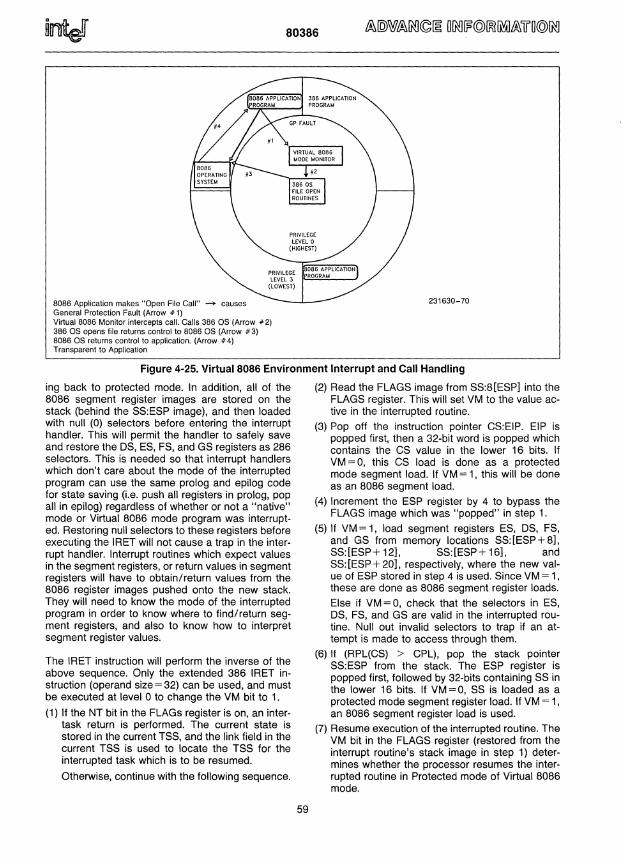
80386
PRIVILEGE LEVEL 0
(HIGHEST)
PRIVILEGE LEVEL 3 F=--.J
8086 Application makes ··Open File Call" -> causes General Protection Fault (Arrow #1)
(LOWEST)
Virtual 8086 Monitor intercepts call. Calls 386 as (Arrow # 2) 386 as opens file returns control to 8086 as (Arrow # 3) 8086 as returns control to application. (Arrow #4) Transparent to Application
231630-70
Figure 4·25. Virtual 8086 Environment Interrupt and Call Handling
ing back to protected mode. In addition, all of the (2) Read the FLAGS image from SS:8[ESP] into the 8086 segment register images are stored on the FLAGS register. This will set VM to the value ac-stack (behind the SS:ESP image), and then loaded tive in the interrupted routine. with null (0) selectors before entering the interrupt (3) Pop off the instruction pointer CS:EIP. EIP is handler. This will permit the handler to safely save popped first, then a 32-bit word is popped which and restore the OS, ES, FS, and GS registers as 286 contains the CS value in the lower 16 bits. If selectors. This is needed so that interrupt handlers VM = 0, this CS load is done as a protected which don't care about the mode of the interrupted mode segment load. If VM = 1, this will be done program can use the same prolog and epilog code as an 8086 segment load. for state saving (i.e. push all registers in prolog, pop (4) Increment the ESP register by 4 to bypass the all in epilog) regardless of whether or not a "native" FLAGS image which was "popped" in step 1. mode or Virtual 8086 mode program was interrupt-ed. Restoring null selectors to these registers before (5) If VM = 1, load segment registers ES, OS, FS, executing the IRET will not cause a trap in the inter- and GS from memory locations SS:[ESP+ 8], rupt handler. Interrupt routines which expect values SS: [ESP + 12], SS: [ESP + 16], and in the segment registers, or return values in segment SS: [ESP + 20], respectively, where the new val-registers will have to obtain/return values from the ue of ESP stored in step 4 is used. Since VM = 1, 8086 register images pushed onto the new stack. these are done as 8086 segment register loads. They will need to know the mode of the interrupted Else if VM = 0, check that the selectors in ES, program in order to know where to find/return seg- OS, FS, and GS are valid in the interrupted rou-ment registers, and also to know how to interpret tine. Null out invalid selectors to trap if an at-segment register values. tempt is made to access through them.
The IRET instruction will perform the inverse of the above sequence. Only the extended 386 IRET instruction (operand size=32) can be used, and must be executed at level 0 to change the VM bit to 1.
(1) If the NT bit in the FLAGs register is on, an intertask return is performed. The current state is stored in the current TSS, and the link field in the current TSS is used to locate the TSS for the interrupted task which is to be resumed.
Otherwise, continue with the following sequence.
59
(6) If (RPL(CS) > CPL), pop the stack pointer SS:ESP from the stack. The ESP register is popped first, followed by 32-bits containing SS in the lower 16 bits. If VM = 0, SS is loaded as a protected mode segment register load. If VM = 1, an 8086 segment register load is used.
(7) Resume execution of the interrupted routine. The VM bit in the FLAGS register (restored from the interrupt routine's stack image in step 1) determines whether the processor resumes the interrupted routine in Protected mode of Virtual 8086 mode.

intJ 80386
5. FUNCTIONAL DATA
5.1 INTRODUCTION
The 80386 features a straightforward functional interface to the external hardware. The 80386 has separate, parallel buses for data and address. The data bus is 32-bits in width, and bidirectional. The address bus outputs 32-bit address values in the most directly usable form for the high-speed local bus: 4 individual byte enable signals, and the 30 upper-order bits as a binary value. The data and address buses are interpreted and controlled with their associated control signals.
A dynamic data bus sizing feature allows the processor to handle a mix of 32- and 16-bit external buses on a cycle-by-cycle basis (see 5.3.4 Data Bus Sizing). If 16-bit bus size is selected, the 80386 automatically makes any adjustment needed, even performing another 16-bit bus cycle to complete the transfer if that is necessary. 8-bit peripheral devices may be connected to 32-bit or 16-bit buses with no loss of performance. A new address pipelining op· tion is provided and applies to 32-bit and 16-bit buses for substantially improved memory utilization, especially for the most heavily used memory resources.
The address pipelining option, when selected, typically allows a given memory interface to operate with one less wait state than would otherwise be required (see 5.4.2 Address Pipelining). The pipelined bus is also well suited to interleaved memory designs. For 16 MHz interleaved memory designs with 100 ns access time DRAMs, zero wait states can be achieved when pipe lined addressing is selected. When address pipelining is requested by the external hardware, the 80386 will output the address and bus cycle definition of the next bus cycle (if it is internally available) even while waiting for the current cycle to be acknowledged.
Non-pipelined address timing, however, is ideal for external cache designs, since the cache memory will typically be fast enough to allow non-pipelined cycles. For maximum design flexibility, the address pipelining option is selectable on a cycle-by-cycle basis.
The processor's bus cycle is the basic mechanism for information transfer, either from system to processor, or from processor to system. 80386 bus cycles perform data transfer in a minimum of only two clock periods. On a 32-bit data bus, the maximum 80386 transfer bandwidth at 16 MHz is therefore 32 Mbytes/sec. Any bus cycle will be extended for more than two clock periods, however, if external hardware withholds acknowledgement of the cycle.
60
At the appropriate time, acknowledgement is signalled by asserting the 80386 READY # input.
The 80386 can relinquish control of its local buses to allow mastership by other devices, such as direct memory access channels. When relinquished, HLDA is the only output pin driven by the 80386, providing near-complete isolation of the processor from its system. The near-complete isolation characteristic is ideal when driving the system from test equipment, and in fault-tolerant applications.
Functional data covered in this chapter describes the processor's hardware interface. First, the set of signals available at the processor pins is described (see 5.2 Signal Description). Following that are the signal waveforms occurring during bus cycles (see 5.3 Bus Transfer Mechanism, 5.4 Bus Functional Description and 5.5 Other Functional Descriptions).
5.2 SIGNAL DESCRIPTION
5.2.1 Introduction
Ahead is a brief description of the 80386 input and output signals arranged by functional groups. Note the # symbol at the end of a signal name indicates the active, or asserted, state occurs when the signal is at a low Voltage. When no # is present after the signal name, the signal is asserted when at the high voltage level.
Example signal: M/IO# - High voltage indicates Memory selected
- Low voltage indicates 1/0 selected
The signal descriptions sometimes refer to AC timing parameters, such as "t25 Reset Setup Time" and "t26 Reset Hold Time." The values of these parameters can be found in Tables 7-4 and 7-5.
5.2.2 Clock (CLK2)
CLK2 provides the fundamental timing for the 80386. It is divided by two internally to generate the internal processor clock used for instruction execution. The internal clock is comprised of two phases, "phase one" and "phase two." Each CLK2 period is a phase of the internal clock. Figure 5-2 illustrates the relationship. If desired, the phase of the internal processor clock can be synchronized to a known phase by ensuring the RESET signal falling edge meets its applicable setup and hold times, t25 and t26·

80386
2X CLOCK [
32-BIT[DO_D31 DATA
BUS [ CONTROL
BUS{ ARBITRATION
INTERRUPTS {
CLK2 ~
< DATA BUS ~ v
ADS#
R~~~: ~ 80386
PROCESSOR
HOLD ~ HLDA
INTR t> NMI t>
RESET t>
ADDRESS BUS BE3#
BE2#
BE1#
BEO#
W/R#
D/C#
M/IO#
LOCK#
PEREQ
I~ BUSY#
~ ERROR#
Vee <l
GND <l
t\
v A2-A31
1 BYTE ENABLES
32-BIT ADDRESS
} COPROCESSOR SIGNALLING
} POWER CONNECTIONS
231630-1
Figure 5-1. Functional Signal Groups
PROCESSOR CLOCK PERIOD
PROCESSOR CLOCK PERIOD
CLK2 PERIOD CLK2 PERIOD CLK2 PERIOD CLK2 PERIOD ~1 ~2 ~1 ~2
CLK2 [
INTERNAL 80386 PROCESSOR CLOCK [
(SAME FREQUENCY AS 82384 CLK SIGNAL)
62 ns MIN} (16 MHz MAX) 80386-16
83 ns MIN} (12.5 MHz MAX) 80386-12
231630-2
Figure 5-2. CLK2 Signal and Internal Processor Clock
5.2.3 Data Bus (DO through 031)
These three-state bidirectional signals provide the general purpose data path between the 80386 and other devices. Data bus inputs and outputs indicate "1" when HIGH. The data bus can transfer data on 32- and 16-bit buses using a data bus sizing feature controlled by the 8S16# input. See section 5.2.6 Bus Conto!. Data bus reads require that read data setup and hold times t21 and t22 be met for correct operation. During any write operation (and during halt cycles and shutdown cycles), the 80386 always drives all 32 signals of the data bus even if the current bus size is 16-bits.
61
5.2.4 Address Bus (BEO# through BE3#, A2 through A31)
These three-state outputs provide physical memory addresses or I/O port addresses. The address bus is capable of addressing 4 gigabytes of physical memory space (OOOOOOOOH through FFFFFFFFH), and 64 kilobytes of I/O address space (OOOOOOOOH through OOOOFFFFH) for programmed I/O. I/O transfers automatically generated for 80386-to-coprocessor communication use I/O addresses 800000F8H through 800000FFH, so A31 HIGH in conjunction with M/IO# LOW allows simple generation of the coprocessor select signal.
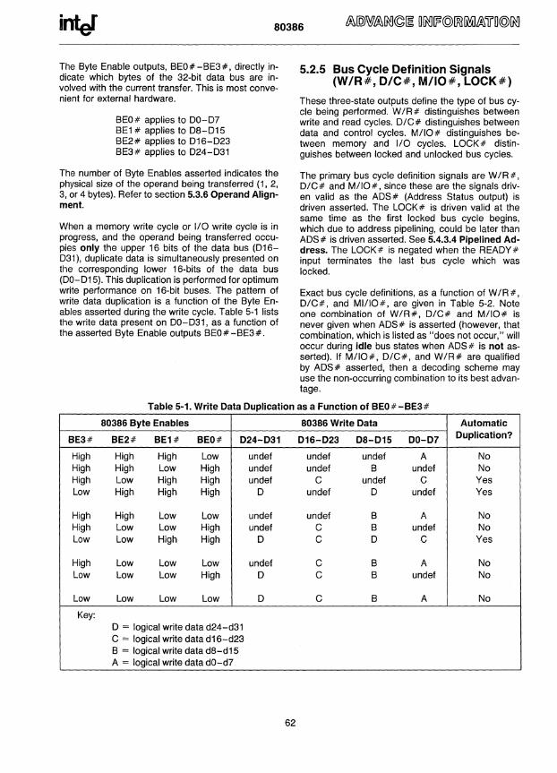
80386
The Byte Enable outputs, BEO#-BE3#, directly indicate which bytes of the 32-bit data bus are involved with the current transfer. This is most convenient for external hardware.
BEO# applies to 00-07 BEl # applies to 08-015 BE2# applies to 016-023 BE3# applies to 024-031
The number of Byte Enables asserted indicates the physical size of the operand being transferred (1, 2, 3, or 4 bytes). Refer to section 5.3.6 Operand Alignment.
When a memory write cycle or 1/0 write cycle is in progress, and the operand being transferred occupies only the upper 16 bits of the data bus (016-031), duplicate data is simultaneously presented on the corresponding lower 16-bits of the data bus (00-D15). This duplication is performed for optimum write performance on 16-bit buses. The pattern of write data duplication is a function of the Byte Enables asserted during the write cycle. Table 5-1 lists the write data present on 00-031, as a function of the asserted Byte Enable outputs BEO#-BE3#.
5.2.5 Bus Cycle Definition Signals (W/R#, D/C#, MIIO#, LOCK#)
These three-state outputs define the type of bus cycle being performed. W /R # distinguishes between write and read cycles. D/C# distinguishes between data and control cycles. M/IO# distinguishes between memory and 1/0 cycles. LOCK# distinguishes between locked and unlocked bus cycles.
The primary bus cycle definition signals are W/R#, O/C# and M/IO#, since these are the signals driven valid as the ADS # (Address Status output) is driven asserted. The LOCK # is driven valid at the same time as the first locked bus cycle begins, which due to address pipelining, could be later than AOS# is driven asserted. See 5.4.3.4 Pipelined Address. The LOCK # is negated when the READY # input terminates the last bus cycle which was locked. .
Exact bus cycle definitions, as a function of W/R#, D/C#, and MI/IO#, are given in Table 5-2. Note one combination of W/R#, D/C# and M/IO# is never given when ADS# is asserted (however, that combination, which is listed as "does not occur," will occur during idle bus states when ADS# is not as-serted). If MIIO#, D/C#, and W/R# are qualified by ADS# asserted, then a decoding scheme may use the non-occurring combination to its best advantage.
Table 5-1 Write Oata Ouplication as a Function of BEO#-BE3#
80386 Byte Enables 80386 Write Oata Automatic
BE3# BE2# BE1# BEO# 024-031 016-023 08-015 00-07 Ouplication?
High High High Low undef undef undef A No High High Low High undef undef B undef No High Low High High undef C undef C Yes Low High High High 0 undef 0 undef Yes
High High Low Low undef undef B A No High Low Low High undef C B undef No Low Low High High D C D C Yes
High Low Low Low undef C B A No Low Low Low High D C B undef No
Low Low Low Low D C B A No
Key: D = logical write data d24-d31 C = logical write data d16-d23 B = logical write data d8-d15 A = logical write data dO-d7
62

80386
Table 5-2 Bus Cycle Definition
MIIO# D/C# W/R# Bus Cycle Type Locked?
Low Low Low INTERRUPT ACKNOWLEDGE Yes
Low Low High does not occur
Low High Low 1/0 DATA READ No
Low High High I/O DATA WRITE No
High Low Low MEMORY CODE READ No
High Low High HALT: SHUTDOWN: No Address = 2 Address = 0
(BEO# High (BEO# Low BE1 # High BE1 # High BE2# Low BE2# High BE3# High BE3# High A2-A31 Low) A2-A31 Low)
High High Low MEMORY DATA READ Some Cycles
High High High MEMORY DATA WRITE Some Cycles
5.2.6 Bus Control Signals
5.2.6.1 INTRODUCTION
The following signals allow the processor to indicate when a bus cycle has begun, and allow other system hardware to control address pipelining, data bus width and bus cycle termination.
5.2.6.2 ADDRESS STATUS (ADS#)
This three-state output indicates that a valid bus cycle definition, and address (W/R#, D/C#, M/IO#, BEO#-BE3#, and A2-A31) is being driven at the 80386 pins. It is asserted during T1 and T2P bus states (see 5.4.3.2 Non-pipelined Address and 5.4.3.4 Pipelined Address for additional information on bus states).
5.2.6.3 TRANSFER ACKNOWLEDGE (READY#)
This input indicates the current bus cycle is complete, and the active bytes indicated by BEO #BE3# and BS16# are accepted or provided. When READY # is sampled asserted during a read cycle or interrupt acknowledge cycle, the 80386 latches the input data and terminates the cycle. When READY # is sampled asserted during a write cycle, the processor terminates the bus cycle.
READY # is ignored on the first bus state of all bus cycles, and sampled each bus state thereafter until asserted. READY # must eventually be asserted to acknowledge every bus cycle, including Halt Indication and Shutdown Indication bus cycles. When be-
63
ing sampled, READY must always meet setup and hold times t19 and t20 for correct operation. See all sections of 5.4 Bus Functional Description.
5.2.6.4 NEKT ADDRESS REQUEST (NA#)
This is used to request address pipelining. This input indicates the system is prepared to accept new values of BEO#-BE3#, A2-A31, W/R#, D/C# and M/IO# from the 80386 even if the end of the current cycle is not being acknowledged on READY #. If th!s input is asserted when sampled, the next address IS
driven onto the bus, provided the next bus request IS
already pending internally. See 5.4.2 Address Pipelining and 5.4.3 Read and Write Cycles.
5.2.6.5 BUS SIZE 16 (BS16#)
The BS16# feature allows the 80386 to directly connect to 32-bit and 16-bit data buses. Asserting this input constrains the current bus cycle to use only the lower-order half (00-015) of the data bus, corresponding to BEO# and BE1 #. Asserting BS16# has no additional effect if only BEO# and/or BE1 # are asserted in the current cycle. However, during bus cycles asserting BE2# or BE3#, asserting BS~6# will automatically cause the 80386. to make adJustments for correct transfer of the upper bytes(s) using only physical data signals DO-D15.
If the operand spans both halves of the data bus and BS 16 # is asserted, the 80386 will automatically perform another 16-bit bus cycle. BS 16 # must always meet setup and hold times t17 and t18 for correct operation.
intJ 80386
80386 I/O cycles automatically generated for coprocessor communication do not require BS16# be asserted. The coprocessor type, 80287 or 80387, is sensed on the ERROR# input shortly after the faIling edge of RESET. The 80386 transfers only 16-bit quantities between itself and the 80287, but must transfer 32-bit quantities between itself and the 80387. Therefore, BS16# is a don't care during 80287 cycles and must not be asserted during 80387 communication cycles.
5.2.7 Bus Arbitration Signals
5.2.7.1 INTRODUCTION
This section describes the mechanism by which the processor relinquishes control of its local buses when requested by another bus master device. See 5.5.1 Entering and Exiting Hold Acknowledge for additional information.
5.2.7.2 BUS HOLD REQUEST (HOLD)
This input indicates some device other than the 80386 requires bus mastership.
HOLD must remain asserted as long as any other device is a local bus master. HOLD is not recognized while RESET is asserted. If RESET is asserted while HOLD is asserted, RESET has priority and places the bus into an idle state, rather than the hold acknowledge (high impedance) state.
HOLD is level-sensitive and is a synchronous input. HOLD signals must always meet setup and hold times t23 and t24 for correct operation.
5.2.7.3 BUS HOLD ACKNOWLEDGE (HLDA)
Assertion of this output indicates the 80386 has relinquished control of its local bus in response to HOLD asserted, and is in the bus Hold Acknowledge state.
The Hold Acknowledge state offers near-complete signal isolation. In the Hold Acknowledge state, HLDA is the only signal being driven by the 80386. The other output signals or bidirectional signals (00-031, BEO#-BE3#, A2-A31, W/R#, D/C#, M/IO#, LOCK# and ADS#) are in a high-impedance state so the requesting bus master may control them. Pull up resistors may be desired on several signals to avoid spurious activity when no bus master is driving them. See 7.2.3 Resistor Recommendations. Also, one rising edge occuring on the NMI input during Hold Ac!mowledge is remembered, for processing after the HOLD input is negated.
64
In addition to the normal usage of Hold Acknowledge with DMA controllers or master peripherals, the near-complete isolation has particular attractiveness during system test when test equipment drives the system, and in hardware-fault-tolerant applications.
5.2.8 Coprocessor Interface Signals
5.2.8.1 INTRODUCTION
In the following sections are descriptions of signals dedicated to the numeric coprocessor interface. In addition to the data bus, address bus, and bus cycle definition signals, these following signals control communication between the 80386 and its 80287 or 80387 processor extension.
5.2.8.2 COPROCESSOR REQUEST (PEREQ)
When asserted, this input signal indicates a coprocessor request for a data operand to be transferred to/from memory by the 80386. In response, the 80386 transfers information between the coprocessor and memory. Because the 80386 has internally stored the coprocessor opcode being executed, it performs the requested data transfer with the correct direction and memory address.
PEREQ is level-sensitive and is allowed to be asynchronous to the CLK2 signal.
5.2.8.3 COPROCESSOR BUSY (BUSY#)
When asserted, this input indicates the coprocessor is still executing an instruction, and is not yet able to accept another. When the 80386 encounters any coprocessor instruction which operates on the numeric stack (e.g. load, pop, or arithmetic operation), or the WAIT instruction, this input is first automatically sampled until it is seen to be negated. This sampling of the BUSY# input prevents overrunning the execution of a previous coprocessor instruction.
The FNINIT and FNCLEX coprocessor instructions are allowed to execute even if BUSY # is asserted; since these instructions are used for coprocessor initialization and exception-clearing.
BUSY # is level-sensitive and is allowed to be asynchronous to the CLK2 signal.
BUSY # serves an additional function. If BUSY # is sampled LOW at the falling edge of RESET, the 80386 performs an internal self-test (see 5.5.3 Bus Activity During and Following Reset). If BUSY # is sampled HIGH, no self-test is performed.

80386
5.2.8.4 COPROCESSOR ERROR (ERROR#)
This input signal indicates that the previous coprocessor instruction generated a coprocessor error of a type not masked by the coprocessor's control register. This input is automatically sampled by the 80386 when a coprocessor instruction is encountered, and if asserted, the 80386 generates exception 16 to access the error-handling software.
Several coprocessor instructions, generally those which clear the numeric error flags in the coprocessor or save coprocessor state, do execute without the 80386 generating exception 16 even if ERROR # is asserted. These instructions are FNINIT, FNCLEX, FSTSW, FSTSWAX, FSTCW, FSTENV, FSAVE, FESTENV and FESAVE.
ERROR # is level-sensitive and is allowed to be asynchronous to the CLK2 signal.
ERROR# serves an additional function. If ERROR# is LOW no later than 20 CLK2 periods after the failing edge of RESET and remains LOW at least until the 80386 begins its first bus cycle, an 80387 is assumed to be present (ET bit in CRO automatically gets set to 1). Otherwise, an 80287 (or no coprocessor) is assumed to be present (ET bit in CRO automatically is reset to 0). See 5.5.3 Bus Activity During and After Reset. Only the ET bit is set by this ERROR# pin test. Software must set the EM and MP bits in CRO as needed. Therefore, distinguishing 80287 presence from no coprocessor requires a software test and appropriately resetting or setting the EM bit of CRO (set EM = 1 when no coprocessor is present). If ERROR# is sampled LOW after reset (indicating 80387) but software later sets EM = 1, the 80386 will behave as if no coprocessor is present.
5.2.9 Interrupt Signals
5.2.9.1 INTRODUCTION
The following descriptions cover inputs that can interrupt or suspend execution of the processor's current instruction stream.
5.2.9.2 MASKABLE INTERRUPT REQUEST (INTR)
When asserted, this input indicates a request for interrupt service, which can be masked by the 80386 Flag Register IF bit. When the 80386 responds to the INTR input, it performs two interrupt acknowledge bus cycles, and at the end of the second, latches an 8-bit interrupt vector on 00-07 to identify the source of the interrupt.
INTR is level-sensitive and is allowed to be asynchronous to the CLK2 signal. To assure recognition
65
of an INTR request, INTR should remain asserted until the first interrupt acknowledge bus cycle begins.
5.2.9.3 NON-MASKABLE INTERRUPT REQUEST (NMI)
This input indicates a request for interrupt service, which cannot be masked by software. The nonmaskable interrupt request is always processed according to the pointer or gate in slot 2 of the interrupt table. Because of the fixed NMI slot assignment, no interrupt acknowledge cycles are perfomed when processing NMI.
NMI is rising edge-sensitive and is allowed to be asynchronous to the CLK2 signal. To assure recognition of NMI, it must be negated for at least eight CLK2 periods, and then be asserted for at least eight CLK2 periods.
Once NMI processing has begun, no additional NMI's are processed until after the next IRET instruction, which is typically the end of the NMI service routine. If NMI is re-asserted prior to that time, however, one rising edge on NMI will be remembered for processing after executing the next. IRET instruction.
5.2.9.4 RESET (RESET)
This input signal suspends any operation in progress and places the 80386 in a known reset state. The 80386 is reset by asserting RESET for 15 or more CLK2 periods (80 or more CLK2 periods before requesting self test). When RESET is asserted, all other input pins are ignored, and all other bus pins are driven to an idle bus state as shown in Table 5-3. If RESET and HOLD are both asserted at a point in time, RESET takes priority even if the 80386 was in a Hold Acknowledge state prior to RESET asserted.
RESET is level-sensitive and must be synchronous to the CLK2 signal. If desired, the phase of the internal processor clock, and the entire 80386 state can be completely synchronized to external circuitry by ensuring the RESET signal falling edge meets its applicable setup and hold times, t25 and t26'
Table 5-3. Pin State (Bus Idle) During Reset
Pin Name Signal Level During Reset
AOS# High 00-031 High Impedance BEO#-BE3# Low A2-A31 High W/R# Low O/C# High M/IO# Low LOCK# High HLOA Low
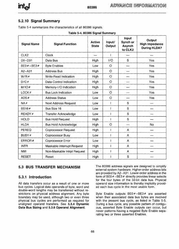
80386
5.2.10 Signal Summary
Table 5-4 summarizes the characteristics of all 80386 signals.
Table 5-4_ 80386 Signal Summary
Signal Name Signal Function
CLK2 Clock
00-031 Data Bus
BEO#-BE3# Byte Enables
A2-A31 Address Bus
W/R# Write-Read Indication
OfC# Data-Control Indication
M/IO# Memory-I/O Indication
LOCK# Bus Lock Indication
ADS# Address Status
NA# Next Address Request
BS16# Bus Size 16
REAOY# Transfer Acknowledge
HOLD Bus Hold Request
HLOA Bus Hold Acknowledge
PEREO Coprocessor Request
BUSY# Coprocessor Busy
ERROR# Coprocessor Error
INTR Maskable Interrupt Request
NMI Non-Maskable Intrpt Request
RESET Reset
5.3 BUS TRANSFER MECHANISM
5.3.1 Introduction
All data transfers occur as a result of one or more bus cycles. Logical data operands of byte, word and double-word lengths may be transferred without restrictions on physical address alignment. Any byte boundary may be used, although two or even three physical bus cycles are performed as required for unaligned operand transfers. See 5_3.4 Dynamic Data Bus Sizing and 5,3.6 Operand Alignment.
Input Output
Active Input! Synch or High Impedance
State Output Asynch During HLDA?
toCLK2
- I - -High 1/0 S Yes
Low 0 - Yes
High 0 - Yes
High 0 - Yes
High 0 - Yes
High 0 - Yes
Low 0 - Yes
Low a - Yes
Low I S -
Low I S -Low I S -High I S -
High a - No
High I A -Low I A -
Low I A -High I A -High I A -High I S -
The 80386 address signals are designed to simplify external system hardware. Higher-order address bits are provided by A2-A31. Lower-order address in the form of BEO# -BE3# directly provides linear selects for the four bytes of the 32-bit data bus. Physical operand size information is thereby implicitly provided each bus cycle in the most usable form.
66
Byte Enable outputs BEO#-BE3# are asserted when their associated data bus bytes are involved with the present bus cycle, as listed in Table 5-5. During a bus cycle, any possible pattern of contiguous, asserted Byte Enable outputs can occur, but never patterns having a negated Byte Enable separating two or three asserted Enables.
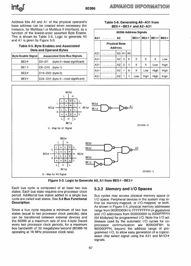
80386
Address bits AO and A1 of the physical operand's base address can be created when necessary (for instance, for Multibus I or Multibus II interface), as a function of the lowest-order asserted Byte Enable. This is shown by Table 5-6. Logic to generate AO and A 1 is given by Figure 5-3.
Table 5-5. Byte Enables and Associated Data and Operand Bytes
Byte Enable Signal Associated Data Bus Signals
BEO# 00-07 (byte O-Ieast significant)
BE1# 08-015 (byte 1)
BE2# 016-023 (byte 2)
BE3# 024-031 (byte 3-most significant)
BEO# L H
L x (HI L L L
A31
A31
A31
A31
A31
A31
Table 5-6. Generating AO-A31 from BEO#-BE3# and A2-A31
80386 Address Signals
......... A2 BE3# BE2# BE1#
Physical Base
Address
" ....... A2 A1 AO
......... A2 0 0 X X X
....... ,' A2 0 1 X X Low
......... A2 1 0 X Low High
......... A2 1 1 Low High High
L x BE2#
L L H
H L
x L H
BEO# ~~ BE3#~
x x H) x L
L H L
BE1# 231630-3
K - Map for A 1 Signal
BEO# L H
L x L H L L
L x L H H
L L x H BE2# BE3#
H x x H x L
L H L
BE1# 231630-4
K - Map for AO Signal
BEO#
Low
High
High
High
Figure 5-3. Logic to Generate AO, A1 from BEO#-BE3#
Each bus cycle is composed of at least two bus states. Each bus state requires one processor clock period. Additional bus states added to a single bus cycle are called wait states. See 5.4 Bus Functional Description.
Since a bus cycle requires a minimum of two bus states (equal to two processor clock periods), data can be transferred between external devices and the 80386 at a maximum rate of one 4-byte Dword every two processor clock periods, for a maximum bus bandwidth of 32 megabytes/second (80386-16 operating at 16 MHz processor clock rate).
67
5.3.2 Memory and 1/0 Spaces
Bus cycles may access physical memory space or I/O space. Peripheral devices in the system may either be memory-mapped, or I/O-mapped, or both. As shown in Figure 5-4, physical memory addresses range from OOOOOOOOH to FFFFFFFFH (4 gigabytes) and I/O addresses from OOOOOOOOH to OOOOFFFFH (64 kilobytes) for programmed I/O. Note the I/O addresses used by the automatic I/O cycles for coprocessor communication are 800000F8H to 800000FFH, beyond the address range of programmed I/O, to allow easy generation of a coprocessor chip select signal using the A31 and M/IO# Signals.
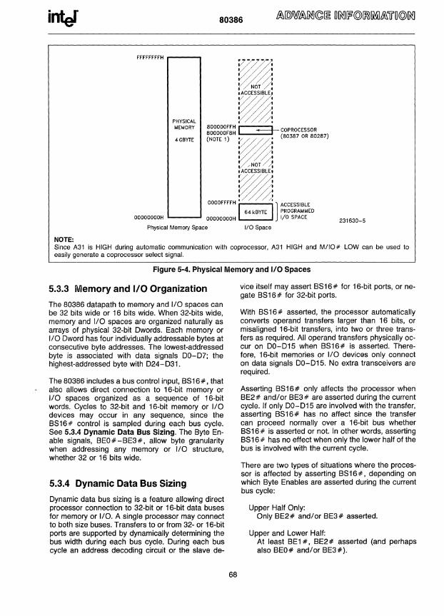
intJ 80386
rrrrrrrrH ...---..,
~1%. ~~ W/ ~ PHYSICAL
MEMORY ~ggggg~~~ I ------:+- COPROCESSOR (NOTE 1) W : (80387 OR 80287) 4GBYTE
V@ /NOT / ),
I ACCESSIBLE.
~ OOOOrrrrH EJ } ACCESSIBLE
64 kBYTE PROGRAMMED OOOOOOOOH I/O SPACE OOOOOOOOH 1..-__ ...1
231630-5 Physical Memory Space 1/0 Space
NOTE: Since A31 is HIGH during automatic communication with coprocessor, A31 HIGH and M/IO# LOW can be used to easily generate a coprocessor select signal.
Figure 5-4. Physical Memory and I/O Spaces
5.3.3 Memory and 110 Organization
The 80386 datapath to memory and I/O spaces can be 32 bits wide or 16 bits wide. When 32-bits wide, memory and I/O spaces are organized naturally as arrays of physical 32-bit Owords. Each memory or I/O Oword has four individually addressable bytes at consecutive byte addresses. The lowest-addressed byte is associated with data signals 00-07; the highest-addressed byte with 024-031.
The 80386 includes a bus control input, B816#, that also allows direct connection to 16-bit memory or 110 spaces organized as a sequence of 16-bit words. Cycles to 32-bit and 16-bit memory or I/O devices may occur in any sequence, since the B816# control is sampled during each bus cycle. 8ee 5.3.4 DynamiC Data Bus Sizing. The Byte Enable signals, BEO # - BE3 #, allow byte granularity when addressing any memory or I/O structure, whether 32 or 16 bits wide.
5.3.4 Dynamic Data Bus Sizing
Dynamic data bus sizing is a feature allowing direct processor connection to 32-bit or 16-bit data buses for memory or I/O. A single processor may connect to both size buses. Transfers to or from 32- or 16-bit ports are supported by dynamically determining the bus width during each bus cycle. During each bus cycle an address decoding circuit or the slave de-
68
vice itself may assert B816 # for 16-bit ports, or negate B816 # for 32-bit ports.
With B816 # asserted, the processor automatically converts operand transfers larger than 16 bits, or misaligned 16-bit transfers, into two or three transfers as required. All operand transfers physically occur on 00-015 when B816# is asserted. Therefore, 16-bit memories or I/O devices only connect on data signals 00-015. No extra transceivers are required.
Asserting B816# only affects the processor when BE2# and/or BE3# are asserted during the current cycle. If only 00-015 are involved with the transfer, asserting B8 16 # has no affect since the transfer can proceed normally over a 16-bit bus whether B816# is asserted or not. In other words, asserting B816# has no effect when only the lower half of the bus is involved with the current cycle.
There are two types of situations where the processor is affected by asserting B816#, depending on which Byte Enables are asserted during the current bus cycle:
Upper Half Only: Only BE2# and/or BE3# asserted.
Upper and Lower Half: At least BE1 #, BE2# asserted (and perhaps also BEO# and/or BE3#).
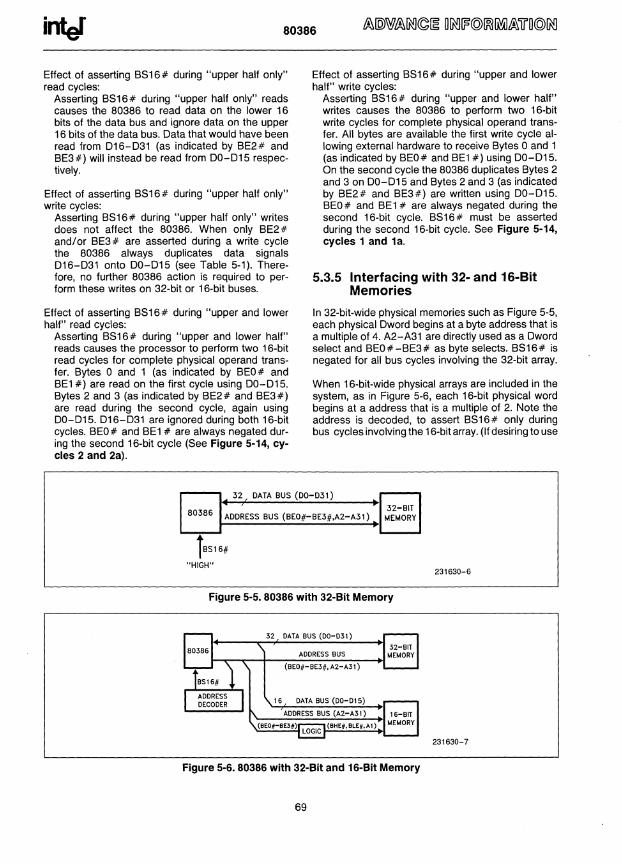
intef 80386
Effect of asserting B516# during "upper half only" read cycles:
Asserting B516# during "upper half only" reads causes the 80386 to read data on the lower 16 bits of the data bus and ignore data on the upper 16 bits of the data bus. Oata that would have been read from 016-031 (as indicated by BE2# and BE3 #) will instead be read from 00-015 respectively.
Effect of asserting B516# during "upper half only" write cycles:
Asserting B516# during "upper half only" writes does not affect the 80386. When only BE2 # and/or BE3# are asserted during a write cycle the 80386 always duplicates data signals 016-031 onto 00-015 (see Table 5-1). Therefore, no further 80386 action is required to perform these writes on 32-bit or 16-bit buses.
Effect of asserting B516# during "upper and lower half" read cycles:
Asserting B516# during "upper and lower half" reads causes the processor to perform two 16-bit read cycles for complete physical operand transfer. Bytes 0 and 1 (as indicated by BEO# and BE1 #) are read on the first cycle using 00-015. Bytes 2 and 3 (as indicated by BE2# and BE3#) are read during the second cycle, again using 00-015. 016-031 are ignored during both 16-bit cycles. BEO# and BE1 # are always negated during the second 16-bit cycle (5ee Figure 5-14, cycles 2 and 2a).
Effect of asserting B516# during "upper and lower half" write cycles:
Asserting B516# during "upper and lower half" writes causes the 80386 to perform two 16-bit write cycles for complete physical operand transfer. All bytes are available the first write cycle allowing external hardware to receive Bytes 0 and 1 (as indicated by BEO# and BE1 #) using 00-015. On the second cycle the 80386 duplicates Bytes 2 and 3 on 00-015 and Bytes 2 and 3 (as indicated by BE2# and BE3#) are written using 00-015. BEO# and BE1 # are always negated during the second 16-bit cycle. B516# must be asserted during the second 16-bit cycle. See Figure 5-14, cycles 1 and 1a.
5.3.5 Interfacing with 32- and 16-Bit Memories
In 32-bit-wide physical memories such as Figure 5-5, each physical Oword begins at a byte address that is a multiple of 4. A2-A31 are directly used as a Oword select and BEO#-BE3# as byte selects. B516# is negated for all bus cycles involving the 32-bit array.
When 16-bit-wide physical arrays are included in the system, as in Figure 5-6, each 16-bit physical word begins at a address that is a multiple of 2. Note the address is decoded, to assert B516# only during bus cycles involving the 16-bit array. (If desiring to use
32 DATA BUS (00-031)
80386 ADDRESS BUS (BEO#-BE3#,A2-A31)
iBS16 #
"HIGH"
32-BIT MEMORY
Figure 5-5. 80386 with 32-Bit Memory
DATA BUS (00-031)
ADDRESS BUS
(BEO#-BE3#, A2-A31)
16 DATA BUS (00-015)
Figure 5-6. 80386 with 32-Bit and 16-Bit Memory
69
231630-6
231630-7
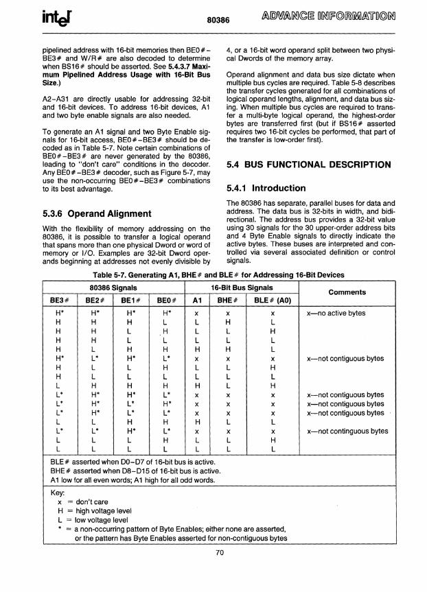
intJ 80386
pipelined address with 16-bit memories then BEO # -BE3 # and W IR # are also decoded to determine when BS16# should be asserted. See 5.4.3.7 Maximum Pipelined Address Usage with 16-Bit Bus Size.)
A2-A31 are directly usable for addressing 32-bit and 16-bit devices. To address 16-bit devices, A1 and two byte enable signals are also needed.
To generate an A1 signal and two Byte Enable signals for 16-bit access, BEO#-BE3# should be decoded as in Table 5-7. Note certain combinations of BEO#-BE3# are never generated by the 80386, leading to "don't care" conditions in the decoder. Any BEO#-BE3# decoder, such as Figure 5-7, may use the non-occurring BEO#-BE3# combinations to its best advantage.
5.3.6 Operand Alignment
With the flexibility of memory addressing on the 80386, it is possible to transfer a logical operand that spans more than one physical Oword or word of memory or 110. Examples are 32-bit Oword operands beginning at addresses not evenly divisible by
4, or a 16-bit word operand split between two physical Owords of the memory array.
Operand alignment and data bus size dictate when multiple bus cycles are required. Table 5-8 describes the transfer cycles generated for all combinations of logical operand lengths, alignment, and data bus sizing. When multiple bus cycles are required to transfer a multi-byte logical operand, the highest-order bytes are transferred first (but if BS16 # asserted requires two 16-bit cycles be performed, that part of the transfer is low-order first).
5.4 BUS FUNCTIONAL DESCRIPTION
5.4.1 Introduction
The 80386 has separate, parallel buses for data and address. The data bus is 32-bits in width, and bidirectional. The address bus provides a 32-bit value using 30 signals for the 30 upper-order address bits and 4 Byte Enable signals to directly indicate the active bytes. These buses are interpreted and controlled via several associated definition or control signals.
Table 5-7. Generating A1, BHE# and BLE# for Addressing 16-Bit Devices
80386 Signals 16-Bit Bus Signals Comments
BE3# BE2# BE1# BEO# A1 BHE# BLE# (AD)
H* H* H* H* x x x x-no active bytes H H H L L H L H H L H L L H H H L L L L L H L H H H H L H* L* H* L* x x x x-not contiguous bytes H L L H L L H H L L L L L L L H H H H L H L* H* H* L* x x x x-not contiguous bytes L* H* L* H* x x x x-not contiguous bytes L* H* L* L* x x x x-not contiguous bytes L L H H H L L L* L* H* L* x x x x-not continguous bytes L L L H L L H L L L L L L L
BLE # asserted when 00-07 of 16-bit bus is active. BHE# asserted when 08-015 of 16-bit bus is active. A 1 low for all even words; A 1 high for all odd words.
Key: x = don't care H = high voltage level L = low voltage level * = a non-occurring pattern of Byte Enables; either none are asserted,
or the pattern has Byte Enables asserted for non-contiguous bytes
70
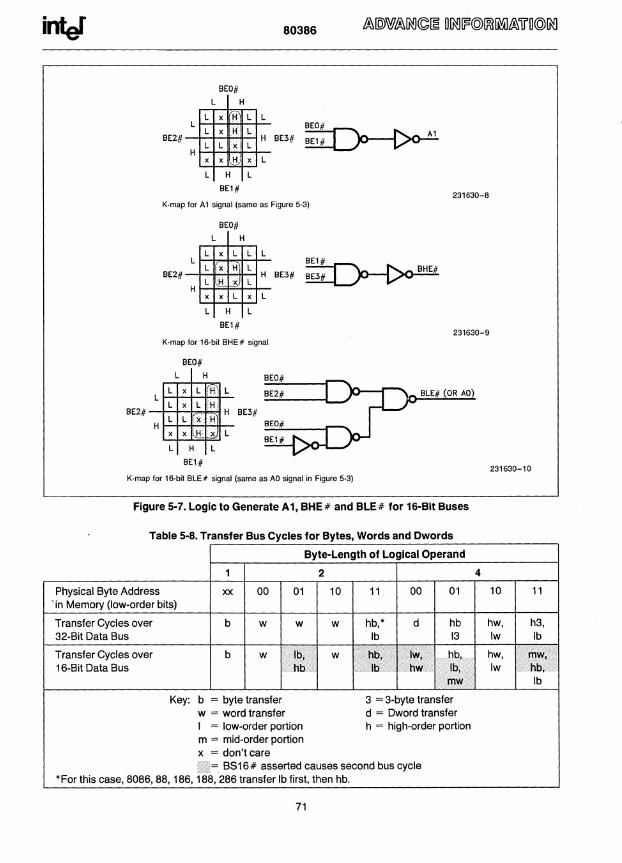
inter 80386
8EO# L H
L x Ii L L
8E2# L
L x H L H
L L ;( L H
H x x x L
[~A1 8E3# 8E1# ----
8EO#
L H L 8E1#
231630-8 K-map for A 1 signal (same as Figure 5-3)
8EO# L H
L x L L L
8E2# L
L x H L
H H
L ·x L H
[~8HE 8[3# 8E3#
--,,--~
8E1#
x x L x L
L H L 8E1#
231630-9 K-map for 16-bit SHE # signal
8EO# L H
L x L H L L
H L x L 8LE# (OR AO)
8E2# H L L X· H
8E3# H
x x H .x L
L H L
8E1# 231630-10
K-map for 16-bit SLE # signal (same as AO signal in Figure 5-3)
Figure 5-7. Logic to Generate A1, BHE# and BLE# for 16-Bit Buses
Table 5-8. Transfer Bus Cycles for Bytes, Words and Dwords
Byte-Length of Logical Operand
1 2 4
Physical Byte Address xx 00 01 10 11 00 01 10 11 -in Memory (low-order bits)
Transfer Cycles over b w w w hb,* d hb hw, h3, 32-Bit Data Bus Ib 13 Iw Ib
Transfer Cycles over b w Ib, w li,'\~~; .. ' Ivv, hb, hw, my", 16-Bit Data Bus hb· •. ... hw Ib, Iw hb;
. JllVi Ib
Key: b = byte transfer 3 = 3-byte transfer w = word transfer d = Dword transfer I = low-order portion h = high-order portion m = mid-order portion x = don't care
= B516# asserted causes second bus cycle 'For this case, 8086, 88, 186, 188, 286 transfer Ib first, then hb.
71
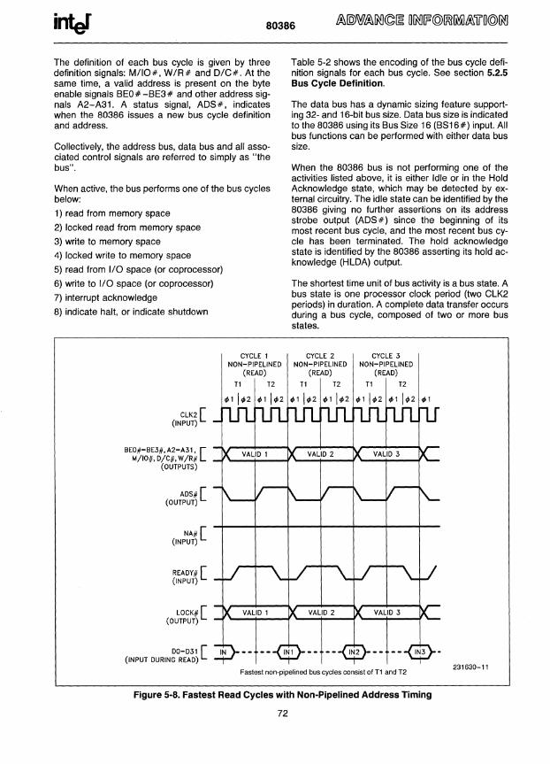
inter 80386
The definition of each bus cycle is given by three definition signals: M/IO#, W/R# and D/C#. At the same time, a valid address is present on the byte enable signals BEO # -BE3 # and other address signals A2-A31. A status signal, ADS#, indicates when the 80386 issues a new bus cycle definition and address.
Collectively, the address bus, data bus and all associated control signals are referred to simply as "the bus".
When active, the bus performs one of the bus cycles below:
1) read from memory space
2) locked read from memory space
3) write to memory space
4) locked write to memory space
5) read from 1/0 space (or coprocessor)
6) write to 1/0 space (or coprocessor)
7) interrupt acknowledge
8) indicate halt, or indicate shutdown
CYCLE 1 NON-PIPELINED
(READ)
Table 5-2 shows the encoding of the bus cycle definition signals for each bus cycle. See section 5.2.5 Bus Cycle Definition.
The data bus has a dynamic sizing feature supporting 32- and 16-bit bus size. Data bus size is indicated to the 80386 using its Bus Size 16 (BS16#) input. All bus functions can be performed with either data bus size.
When the 80386 bus is not performing one of the activities listed above, it is either Idle or in the Hold Acknowledge state, which may be detected by external circuitry. The idle state can be identified by the 80386 giving no further assertions on its address strobe output (ADS#) since the beginning of its most recent bus cycle, and the most recent bus cycle has been terminated. The hold acknowledge state is identified by the 80386 asserting its hold acknowledge (HLDA) output.
The shortest time unit of bus activity is a bus state. A bus state is one processor clock period (two CLK2 periods) in duration. A complete data transfer occurs during a bus cycle, composed of two or more bus states.
CYCLE 2 NON-PIPELINED
(READ)
CYCLE 3 NON-PIPELINED
(READ)
T1 T2 T1 T2 T1 T2
CLK2 [ (INPUT)
8EO#-8E3#, A2-A31, [ M/IO#, D/C#, WjR#
(OUTPUTS)
ADS# [ (OUTPUT)
NA# [ (INPUT)
READY# [ (INPUT)
LOCK# [ (OUTPUT)
00-031 [ (INPUT DURING READ)
.p1 1.p2 .p1 1.p2 .p1 1.p2 .p1 1.p2 .p1 1.p2 .p1 1.p2 .p1
Fastest non·pipelined bus cycles consist of T1 and T2
Figure 5·8. Fastest Read Cycles with Non·Pipelined Address Timing
72
231630-11

80386
The fastest 80386 bus cycle requires only two bus states. For example, three consecutive bus read cycles, each consisting of two bus states, are shown by Figure 5-8. The bus states in each cycle are named T1 and T2. Any memory or 1/0 address may be accessed by such a two-state bus cycle, if the external hardware is fast enough. The high-bandwidth, two-clock bus cycle realizes the full potential of fast main memory, or cache memory.
Every bus cycle continues until it is acknowledged by the external system hardware, using the 80386 READY # input. Acknowledging the bus cycle at the end of the first T2 results in the shortest bus cycle, requiring only T1 and T2. If READY # is not immediately asserted, however, T2 states are repeated indefinitely until the READY # input is sampled asserted.
5.4.2 Address Pipelining
The address pipelining option provides a choice of bus cycle timings. Pipelined or non-pipelined address timing is selectable on a cycle-by-cycle basis with the Next Address (NA#) input.
CLK2[ (INPUT)
BED#-BE3#.A2-A31. [ M/IO#. D/C#. W/R#
(OUTPUTS)
ADS#[ (OUTPUT)
NA# [ (INPUT)
READY# [ (INPUT)
LOCK# [ (OUTPUT)
00-031 [ (INPUT DURING READ)
CYCLE 1 PIPELINED
(READ)
T1P T2P
When address pipelining is not selected, the current address and bus cycle definition remain stable throughout the bus cycle.
When address pipelining is selected, the address (BEO#-BE3#, A2-A31) and definition (W/R#, D/C# and M/IO#) of the next cycle are available before the end of the current cycle. To signal their availability, the 80386 address status output (ADS#) is also asserted. Figure 5-9 illustrates the fastest read cycles with pipe lined address timing.
Note from Figure 5-9 the fastest bus cycles using pipelined address require only two bus states, named T1P and T2P. Therefore cycles with pipelined address timing allow the same data bandwidth as non-pipelined cycles, but address-to-data access time is increased compared to that of a non-pipelined cycle.
By increasing the address-to-data access time, pipelined address timing reduces wait state requirements. For example, if one wait state is required with non-pipelined address timing, no wait states would be required with pipelined address.
CYCLE 2 PIPELINED
(READ)
T1P T2P
CYCLE 3 PIPELINED
(READ)
T1P T2P
Fastest pipelined bus cycles consist of T1 P and T2P 231630-12
Figure 5·9. Fastest Read Cycles with Pipelined Address Timing
73
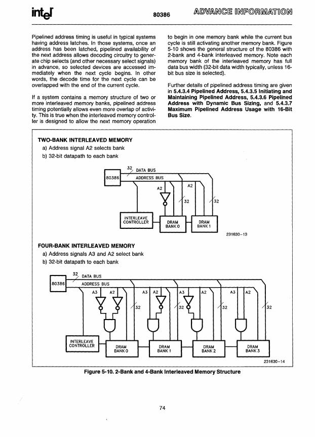
inter 80386
Pipelined address timing is useful in typical systems having address latches. In those systems, once an address has been latched, pipelined availability of the next address allows decoding circuitry to generate chip selects (and other necessary select signals) in advance, so selected devices are accessed immediately when the next cycle begins. In other words, the decode time for the next cycle can be overlapped with the end of the current cycle.
If a system contains a memory structure of two or more interleaved memory banks, pipelined address timing potentially allows even more overlap of activity. This is true when the interleaved memory controller is designed to allow the next memory operation
TWO-BANK INTERLEAVED MEMORY a) Address signal A2 selects bank
b) 32-bit datapath to each bank
FOUR-BANK INTERLEAVED MEMORY
a) Address signals A3 and A2 select bank
b) 32-bit datapath to each bank
to begin in one memory bank while the current bus cycle is still activating another memory bank. Figure 5-10 shows the general structure of the 80386 with 2-bank and 4-bank interleaved memory. Note each memory bank of the interleaved memory has full data bus width (32-bit data width typically, unless 16-bit bus size is selected).
Further details of pipelined address timing are given in 5.4.3.4 Pipelined Address, 5.4.3.5 Initiating and Maintaining Pipelined Address, 5.4.3.6 Pipelined Address with Dynamic Bus Sizing, and 5.4.3.7 Maximum Pipelined Address Usage with 16-Bit Bus Size.
231630-13
231630-14
Figure 5-10. 2-Bank and 4-Bank Interleaved Memory Structure
74

inter 80386
5.4.3 Read and Write Cycles
5.4.3.1 INTRODUCTION
Data transfers occur as a result of bus cycles, classified as read or write cycles. During read cycles, data is transferred from an external device to the processor. During write cycles data is transferred in the other direction, from the processor to an external device.
Two choices of address timing are dynamically selectable: non-pipe lined, or pipe lined. After a bus idle state, the processor always uses non-pipelined ~ddress timing. However, the NA# (Next Address) input may be asserted to select pipelined address timing for the next bus cycle. When pipelining is selected and the 80386 has a bus request pending internally, the address and definition of the next cycle !s made available even before the current bus cycle IS
acknowledged by READY#. Generally, the NA# input is sampled each bus cycle to select the desired address timing for the next bus cycle.
Two choices of physical data bus width are dynamically selectable: 32 bits, or 16 bits. Generally, the B816# (Bus 8ize 16) input is sampled near the end of the bus cycle to confirm the physical data bus size applicable to the current cycle. Negation of B816# indicates a 32-bit size, and assertion indicates a 16-bit bus size.
If 16-bit bus size is indicated, the 80386 automatically responds as required to complete the transfer on a 16-bit data bus. Depending on the size and alignment of the operand, another 16-bit bus cycle may be required. Table 5-7 provides all details. When necessary, the 80386 performs an additional 16-bit bus cycle, using 00-015 in place of 016-031.
Terminating a read cycle or write cycle, like any bus cycle, requires acknowledging the cycle by asserting the READY # input. Until acknowledged, the processor inserts wait states into the bus cycle, to allow adjustment for the speed of any external device. External hardware, which has decoded the address and bus cycle type asserts the READY # input at the appropriate time.
IDLE [
CYCLE 1 NON-PIPELINED
(WRITE)
CYCLE 2 [ NON-PIPELINED
(READ)
CYCLE 3 [IDLE [ CYCLE 4 [IDLE [ NON-PIPELINED NON-PIPELINED
(WRITE) (READ)
ClK2 [
(82384 ClK) [
BED #-BE3 # [ A2- A31,
M/IO#,O/C#
Ti
W/R# [ ~~9'
ADS# [
READY # [
00- 031 [
T1 T2 T1 T2 T1 T2 Ti T1 T2 Ti
231630-15 Idle states are shown here for diagram variety only. Write cycles are not always fallowed by an idle state. An active bus cycle can immediately follow the write cycle.
Figure 5-11. Various Bus Cycles and Idle States with Non-Pipelined Address (zero wait states)
75
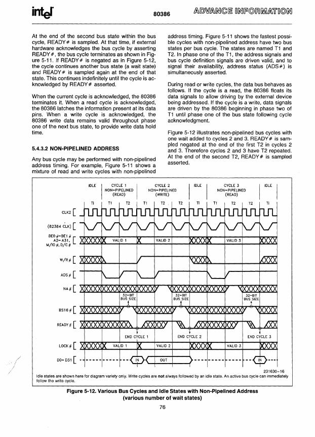
,/ /
/
80386
At the end of the second bus state within the bus cycle, READY # is sampled. At that time, if external hardware acknowledges the bus cycle by asserting READY #, the bus cycle terminates as shown in Figure 5-11. If READY # is negated as in Figure 5-12, the cycle continues another bus state (a wait state) and READY # is sampled again at the end of that state. This continues indefinitely until the cycle is acknowledged by READY # asserted.
When the current cycle is acknowledged, the 80386 terminates it. When a read cycle is acknowledged, the 80386 latches the information present at its data pins. When a write cycle is acknowledged, the 80386 write data remains valid throughout phase one of the next bus state, to provide write data hold time.
5.4.3.2 NON-PIPELINED ADDRESS
Any bus cycle may be performed with non-pipelined address timing. For example, Figure 5-11 shows a mixture of read and write cycles with non-pipe lined
address timing. Figure 5-11 shows the fastest possible cycles with non-pipelined address have two bus states per bus cycle. The states are named T1 and T2. In phase one of the T1, the address signals and bus cycle definition signals are driven valid, and to signal their availability, address status (ADS#) is simultaneously asserted.
During read or write cycles, the data bus behaves as follows. If the cycle is a read, the 80386 floats its data signals to allow driving by the external device being addressed. If the cycle is a write, data signals are driven by the 80386 beginning in phase two of T1 until phase one of the bus state following cycle acknowledgment.
Figure 5-12 illustrates non-pipelined bus cycles with one wait added to cycles 2 and 3. READY# is sampled negated at the end of the first T2 in cycles 2 and 3. Therefore cycles 2 and 3 have T2 repeated. At the end of the second T2, READY # is sampled asserted.
IDLE I CYCLE 1 I NON-PIPElINED
(READ)
CYCLE 2 NON-PIPELINED
(WRITE)
CYCLE 3 NON-PIPELINED
(READ)
n Tl T2 T1 T2 T2 n T1 T2 T2 Ti
ClK2 [ -rut rut rut rut il..fl ilJl.. nn. nn rut 1.fl rut (82384 elK) [
8EO#-8El # [ A2-A31.
M/IO N,D/CN
W/R# [
ADSN [
NA# [
8516 # [
READYN [
lOCK # [
00- 031 [
-V V V V \J \J \f V \J \J V X XX IX VALID 1 IX VALID 2 XXXXX VALID 3 IXXXX
XXXI), / ,,(XXXIX. ~
i'-r-"-.-1 ~/
IXXX IX XXX XXXX XXXXy "( XXX XX IXXX ~XXXX IXXXX 52-BIT 52-BIT 52-BIT
BuStZE BUStZE BUStZE
XIXXXX IXXXXY ~XXXX xXXX rY "(IXXXX IXXX)( XXXXrY '<~
XXXXX IXXXX XXA .(XX IXXY ~ .(XX IXXXX XXrY ~ n:x END CYCLE 1 END CYCLE 2 END CYCLE 3
XX VALID 1 IX VALID 2 IXXX VALID 3 IXXXX
. ----------~--¢< OUT }--------- ---- --¢---231630-16
Idle states are shown here for diagram variety only. Write cycles are not always followed by an idle state. An active bus cycle can immediately follow the write cycle.
Figure 5·12. Various Bus Cycles and Idle States with Non-Pipelined Address (various number of wait states)
76

intJ 80386
HOLD ASSERTED
REQUEST PENDING. HOLD NEGATED
Bus States:
ALWAYS
READY# ASSERTED' HOLD NEGATED'
REQUEST PENDING
READY# NEGATED' NA# NEGATED
Tl-first clock of a non-pipelined bus cycle (80386 drives new address and asserts ADS#) T2-subsequent clocks of a bus cycle when NA # has not been sampled asserted in the current bus cycle
231630-17
Ti- idle state Th-hold acknowledge state (80386 asserts HLDA) The fastest bus cycle consists of two states: Tl and T2. Four basic bus states describe bus operation when not using pipelined address. These states do include 8S16 # usage for 32-bit and 16-bit bus size. If asserting 8S16# requires a second 16-bit bus cycle to be performed, it is performed before HOLD asserted is acknowledged.
Figure 5-13_ 80386 Bus States (not usIng pipelined address)
When address pipelining is not used, the address and bus cycle definition remain valid during all wait states. When wait states are added and you desire to maintain non-pipelined address timing, it is necessary to negate NA# during each T2 state except the last one, as shown in Figure 5-12 cycles 2 and 3. If NA# is sampled asserted during a T2 other than the last one, the next state would be T21 (for pipe lined address) or T2P (for pipelined address) instead of another T2 (for non-pipelined address).
When address pipelining is not used, the bus states and transitions are completely illustrated by Figure 5-13. The bus transitions between four possible states: T1, T2, Ti, and Th. Bus cycles consist of T1 and T2, with T2 being repeated for wait states. Otherwise, the bus may be idle, in the Ti state, or in hold acknowledge, the Th state.
When address pipelining is not used, the bus state diagram is as shown in Figure 5-13. When the bus is
77
idle it is in state Ti. Bus cycles always begin with T1. T1 always leads to T2. If a bus cycle is not acknowledged during T2 and NA# is negated, T2 is repeated. When a cycle is acknowledged during T2, the following state will be T1 of the next bus cycle if a bus request is pending internally, or Ti if there is no bus request pending, or Th if the HOLD input is being asserted.
The bus state diagram in Figure 5-13 also applies to the use of B516#. If the B03B6 makes internal adjustments for 16-bit bus size, the adjustments do not affect the external bus states. If an additional 16-bit bus cycle is required to complete a transfer on a 16-bit bus, it also follows the state transitions shown in Figure 5-13.
Use of pipe lined address allows the 803B6 to enter three additional bus states not shown in Figure 5-13. Figure 5-20 in 5.4.3.4 Pipelined Address is the complete bus state diagram, including pipelined address cycles.
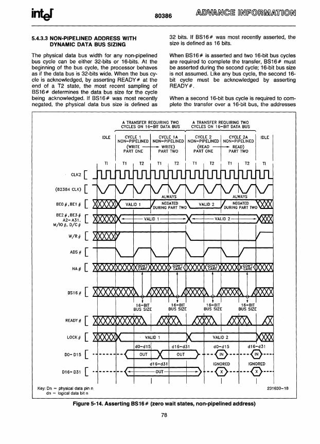
inter 80386
5.4.3.3 NON·PIPELINED ADDRESS WITH DYNAMIC DATA BUS SIZING
The physical data bus width for any non-pipelined bus cycle can be either 32-bits or 16-bits. At the beginning of the bus cycle, the processor behaves as if the data bus is 32-bits wide. When the bus cycle is acknowledged, by asserting READY # at the end of a T2 state, the most recent sampling of 8S16# determines the data bus size for the cycle being acknowledged. If 8S16# was most recently negated, the physical data bus size is defined as
32 bits. If 8S16# was most recently asserted, the size is defined as 16 bits.
When 8S 16 # is asserted and two 16-bit bus cycles are required to complete the transfer, 8S16# must be asserted during the second cycle; 16-bit bus size is not assumed. Like any bus cycle, the second 16-bit cycle must be acknowledged by asserting READY#.
When a second 16-bit bus cycle is required to complete the transfer over a 16-bit bus, the addresses
A TRANSFER REQUIRING TWO CYCLES ON 16-BIT DATA BUS
A TRANSFER REQUIRING TWO CYCLES ON 16-BIT DATA BUS
CLK2 [
(82384 CLK) [ BEO#,BEl # [ BE2 # ,BE3 # [ A2- A31.
M/IO#.D/C#
W/R# [
ADS # [
NA# [
BS16 # [
READY # [ LOCK# [
00- 015 [
IDLE
Ti
CYCLE 1 tCYCLE 1 A NON-PIPELINED NON-PIPELINED
(WRITE WRITE) PART ONE PART TWO
T1 T2 T1 T2
CYCLE 2 TCYCLE 2A NON-PIPELINED NON-PIPELINED
(READ READ) PART ONE PART TWO
T1 T2 T1 T2
IDLE
Ti
016-031 [ • -------<:t==~O~U~T~==t=) IGNORED IGNORED
--0-- ---0---Key: Dn ~ physical data pin n
dn ~ logical data bit n
I I
Figure 5·14; Asserting BS16# (zero wait states, non·pipelined address)
78
231630-18

inter
IDLE
Ti
CLK2 [ -M (82384 CLK) [
-V
80386
A TRANSFER REQUIRING TWO CYCLES ON 16-81T DATA BUS
CYCLE 1 CYCLE 1 A NON-PIPELINED NON-PIPELINED
(READ ----!---READ) PART ONE PART TWO
T1 T2 T 2 T I T2 T2
nIL M rm rtJl nIL nIL V V V V V V
CYCLE 2 NON-PIPELINED
(WRITE)
T1 T2 T2
nIL rtJl nIL V V V
8EO #. 8El # [
[
XIXXXXX VALID I I NEGATED DURING i\ VALID 2 PART TWO
8E2 #. 8E3 # A2- A31.
M/IO#. D/C#
W/R# [
ADS# [
J.lXX.X) X
~ ~
LV
I
VALID I VALID 2
/
"---I "---V N TE: NA# MUST BE NEGATED
HERE TO ALLOW RECOGNITION OF ASSERTED BSI6# IN FINAL T2
NA# [ XIXXXX ,XXXXY '< X~~~~ DOO()(¥ 'X ~~~~~{ XXXX rY '( XXX ~
BUS ~ZE
BSI6# [ )[XXX :XX'x XXX X ).. " IXXXX wOO< ~ J, XXX XXX '1/ '\ 16-BIT 16-81T
BUS SIZE BUS SIZE
READY # [ ) XXX) DOOC <XI ~ I IX) 'XY ~I IX 'XI ~ LOCK# [ )( Y.'J.'X'J. ~ VALID I VALID 2
dO-dl5 d16-d31 dO-dl5
DO- D15 [ - ---- ---- --- --0-- --- --0< OUT
IGNORED IGNORED d16-d31
D16- D31 [ - ---- ---- --_. --0-- --- --0 OUT
Key: On = physical data pin n dn = logical data bit n
I I I 231630-19
Figure 5-15. Asserting 8S16# (one wait state, non-pipelined address)
generated for the two 16-bit bus cycles are closely related to each other. The addresses are the same except 8EO# and 8E1 # are always negated for the second cycle. This is because data on DO-D15 was already transferred during the first 16-bit cycle.
Figures 5-14 and 5-15 show cases where assertion of 8816# requires a second 16-bit cycle for complete operand transfer. Figure 5-14 illustrates cycles
79
without wait states. Figure 5-15 illustrates cycles with one wait state. In Figure 5-15 cycle 1, the bus cycle during which 8816# is asserted, note that NA# must be negated in the T2 state(s) prior to the last T2 state. This is to allow the recognition of 8816# asserted in the final T2 state. The relation of NA# and 8816# is given fully in 5.4.3.4 Pipelined Address, but Figure 5-15 illustrates this only precaution you need to know when using 8816# with non-pipelined address.
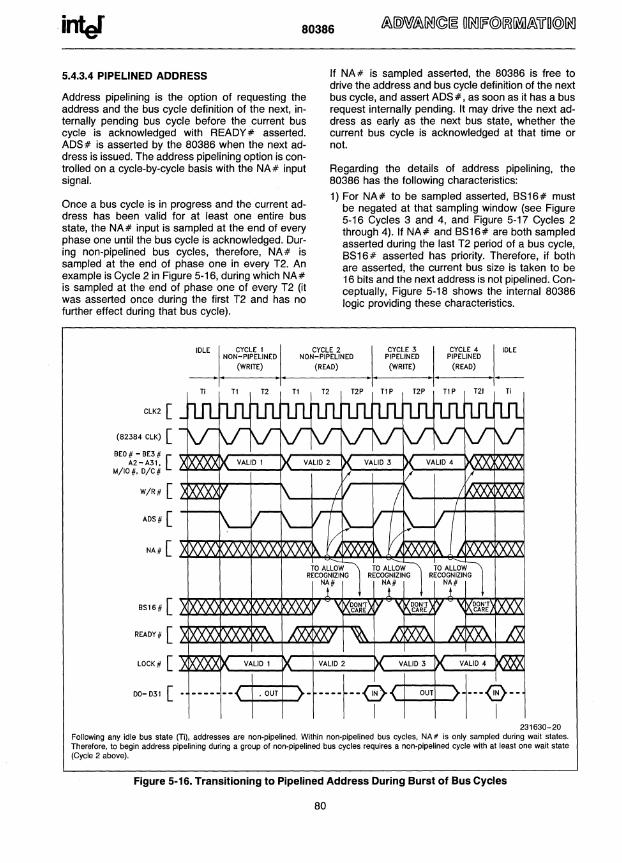
80386
5.4.3.4 PIPELINED ADDRESS
Address pipelining is the option of requesting the address and the bus cycle definition of the next, internally pending bus cycle before the current bus cycle is acknowledged with READY # asserted. AD5# is asserted by the 80386 when the next address is issued. The address pipelining option is controlled on a cycle-by-cycle basis with the NA # input signal.
Once a bus cycle is in progress and the current address has been valid for at least one entire bus state, the NA# input is sampled at the end of every phase one until the bus cycle is acknowledged. During non-pipelined bus cycles, therefore, NA# is sampled at the end of phase one in every T2. An example is Cycle 2 in Figure 5-16, during which NA # is sampled at the end of phase one of every T2 (it was asserted once during the first T2 and has no further effect during that bus cycle).
If NA # is sampled asserted, the 80386 is free to drive the address and bus cycle definition of the next bus cycle, and assert ADS #, as soon as it has a bus request internally pending. It may drive the next address as early as the next bus state, whether the current bus cycle is acknowledged at that time or not.
Regarding the details of address pipelining, the 80386 has the following characteristics:
1) For NA# to be sampled asserted, 8516# must be negated at that sampling window (see Figure 5-16 Cycles 3 and 4, and Figure 5-17 Cycles 2 through 4). If NA# and 8516# are both sampled asserted during the last T2 period of a bus cycle, 8516# asserted has priority. Therefore, if both are asserted, the current bus size is taken to be 16 bits and the next address is not pipelined. Conceptually, Figure 5-18 shows the internal 80386 logic providing these characteristics.
IDLE CYCLE 1 NON-PIPELINED
CYCLE 2 NON-PIPELINED
CYCLE 3 PIPELINED (WRITE)
CYCLE 4 PIPELINED
IDLE
CLK2 [
(82384 CLK) [
n
(WRITE)
TI T2 TI
(READ) (READ)
T2 T2P TIP T2P TI P T21 n
BEO # - BE3 # [ ~""""V'-::-::7.:"'7'""--1\ A2-A31,
MilO #. DIC # '------f )---:---f' >-...,;;,,;::.:....~r)'~~~
W/R# [
AD5# [
B516# [ ~~..t::J.~~~~~~~
READY # [ ~UI..~"!I'-~UI!oLlil~""'~,+;s.,,)I
00- 031 [
231630-20 Following any idle bus state (Ti). addresses are non·pipelined. Within non·pipelined bus cycles. NA" is only sampled during wait states. Therefore. to begin address pipelining during a group of non·pipelined bus cycles requires a non'pipelined cycle with at least one wait state (Cycle 2 above).
Figure 5-16. Transitioning to Pipelined Address During Burst of Bus Cycles
80

intJ 80386
IDLE CYCLE 1 NON-PIPELINED
(WRITE)
CYCLE 2 PIPELINED
(READ)
CYCLE 3 PIPELINED (WRITE)
CYCLE 4 PIPELINED
(READ)
IDLE
Ti n T2 T2P np T2P n P T2P T1P T21 T21 Ti
ClK2 [
(82384 ClK) [
BEO #- BD #' [ A2-A31,
M/IO#, D/C#
W /R # [ 44'..¥-l~.J(
ADS# [
BS16 # [ 44~~~...l'-.lI...l>(
READY # [ 44~~""''"''".lI...l/l-'''''
DO- D31 [
231630-21 Following any idle bus state (Ti) the address is always non-pipelined and NA# is only sampled during wait states. To start address pipelining after an idle state requires a non-pipelined cycle with at least one wait state (cycle 1 above). The pipelined cycles (2, 3, 4 above) are shown with various numbers of wait states.
Figure 5-17. Fastest Transition to Pipelined Address Following Idle Bus State
2) The next address may appear as early as the bus state after NA# was sampled asserted (see Figures 5-16 or 5-17). In that case, state T2P is entered immediately_ However, when there is not an internal bus request already pending, the next address will not be available immediately after NA# is asserted and T21 is entered instead of T2P (see Figure 5-19 Cycle 3)_ Provided the current bus cycle isn't yet acknowledged by READY # asserted, T2P will be entered as soon as the 80386 does drive the next address. External hardware should therefore observe the AD8# output as confirmation the next address is actually being driven on the bus.
3) Once NA# is sampled asserted, the 80386 commits itself to the highest priority bus request that is pending internally_ It can no longer perform another 16-bit transfer to the same address should
81
8816# be asserted externally, so thereafter must assume the current bus size is 32 bits. Therefore if NA# is sampled asserted within a bus cycle, 8816# is ignored thereafter in that bus cycle (see Figures 5-16, 5-17, 5-19)_ Consequently, do not assert NA# during bus cycles which must have 8816# driven asserted. 8ee 5.4.3.6 Dynamic Bus Sizing with Pipelined Address.
4) Any address which is validated by a pulse on the 80386 AD8# output will remain stable on the address pins for at least two processor clock periods. The 80386 cannot produce a new address more frequently than every two processor clock periods (see Figures 5-16, 5-17, 5-19).
5) Only the address and bus cycle definition of the very next bus cycle is available. The pipelining capability cannot look further than one bus cycle ahead (see Figure 5-19 Cycle 1).
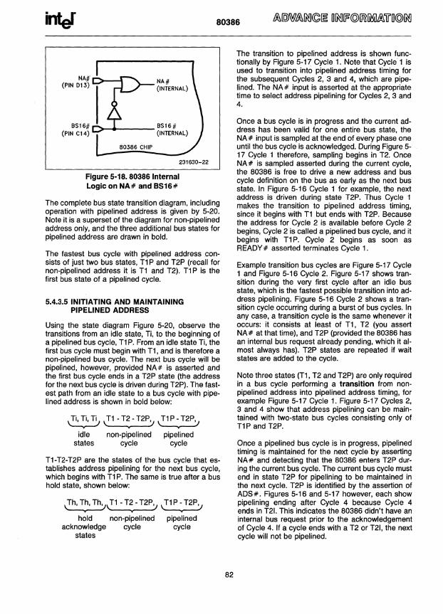
inter 80386
NA#' (PIN 013) D--4 NA#
(INTERNAL)
9S16# c:_ ..... ---- 9S16 # (PIN C14) (INTERNAL)
231630-22
Figure 5-18. 80386 Internal Logic on NA# and 8516#
The complete bus state transition diagram, including operation with pipelined address is given by 5-20. Note it is a superset of the diagram for non-pipelined address only, and the three additional bus states for pipelined address are drawn in bold.
The fastest bus cycle with pipelined address consists of just two bus states, T1 P and T2P (recall for non-pipelined address it is T1 and T2). T1 P is the first bus state of a pipelined cycle.
5.4.3.5 INITIATING AND MAINTAINING PIPELINED ADDRESS
Using the state diagram Figure 5-20, observe the transitions from an idle state, Ti, to the beginning of a pipelined bus cycle, T1 P. From an idle state Ti, the first bus cycle must begin with T1, and is therefore a non-pipelined bus cycle. The next bus cycle Will be pipelined, however, provided NA# is asserted and the first bus cycle ends in a T2P state (the address for the next bus cycle is driven during T2P). The fastest path from an idle state to a bus cycle with pipelined address is shown in bold below:
~ ,T1-T~-T2P'J ,T1P:T2P'J
idle non-pipelined pipelined states cycle cycle
T1-T2-T2P are the states of the bus cycle that establishes address pipelining for the next bus cycle, which begins with T1 P. The same is true after a bus hold state, shown below:
,Th, Th, Th')l..T1 - T2 - T2P'J ,T1 P - T2P'J T 'f' T
hold non-pipelined acknowledge cycle
states
pipelined cycle
82
The transition to pipelined address is shown functionally by Figure 5-17 Cycle 1. Note that Cycle 1 is used to transition into pipelined address timing for the subsequent Cycles 2, 3 and 4, which are pipelined. The NA# input is asserted at the appropriate time to select address pipelining for Cycles 2, 3 and 4.
Once a bus cycle is in progress and the current address has been valid for one entire bus state, the NA# input is sampled at the end of every phase one until the bus cycle is acknowledged. During Figure 5-17 Cycle 1 therefore, sampling begins in T2. Once NA# is sampled asserted during the current cycle, the 80386 is free to drive a new address and bus cycle definition on the bus as early as the next bus state. In Figure 5-16 Cycle 1 for example, the next address is driven during state T2P. Thus Cycle 1 makes the transition to pipelined address timing, since it begins with T1 but ends with T2P. Because the address for Cycle 2 is available before Cycle 2 begins, Cycle 2 is called a pipelined bus cycle, and it begins with T1 P. Cycle 2 begins as soon as READY # asserted terminates Cycle 1.
Example transition bus cycles are Figure 5-17 Cycle 1 and Figure 5-16 Cycle 2. Figure 5-17 shows transition during the very first cycle after an idle bus state, which is the fastest possible transition into address pipelining. Figure 5-16 Cycle 2 shows a transition cycle occurring during a burst of bus cycles. In any case, a transition cycle is the same whenever it occurs: it consists at least of T1, T2 (you assert NA# at that time), and T2P (provided the 80386 has an internal bus request already pending, which it almost always has). T2P states are repeated if wait states are added to the cycle.
Note three states (T1, T2 and T2P) are only required in a bus cycle performing a transition from nonpipelined address into pipelined address timing, for example Figure 5-17 Cycle 1. Figure 5-17 Cycles 2, 3 and 4 show that address pipelining can be maintained with two-state bus cycles consisting only of T1P and T2P.
Once a pipelined bus cycle is in progress, pipelined timing is maintained for the next cycle by asserting NA# and detecting that the 80386 enters T2P during the current bus cycle. The current bus cycle must end in state T2P for pipelining to be maintained in the next cycle. T2P is identified by the assertion of ADS#. Figures 5-16 and 5-17 however, each show pipelining ending after Cycle 4 because Cycle 4 ends in T21. This indicates the 80386 didn't have an internal bus request prior to the acknowledgement of Cycle 4. If a cycle ends with a T2 or T21, the next cycle will not be pipelined.
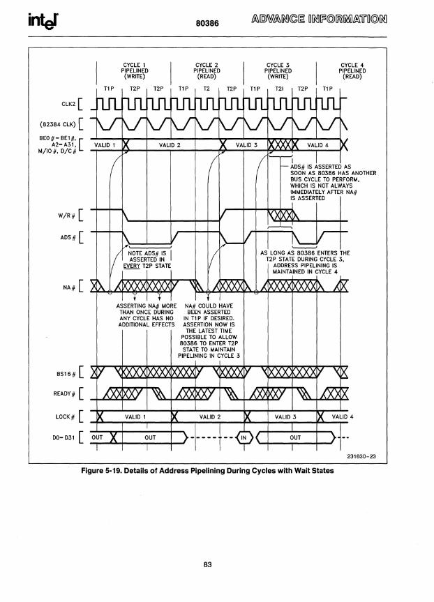
inter
CLK2 [
(82384 ClK) [
BED # - BE 1 #, [ A2- A31,
M/IO#, D/c#
W/R# [
ADS# [
8S16 # [
READY# [
lOCK# [
DO- D31 [
TlP
CYCLE 1 PIPELINED (WRITE)
T2P T2P
ASSERTING NA# MORE THAN ONCE DURING ANY CYCLE HAS NO ADDITIONAL EFFECTS
T1P
80386
CYCLE 2 PIPELINED
(READ)
T2 T2P
NA# COULD HAVE BEEN ASSERTED
IN Tl P IF DESIRED. ASSERTION NOW IS THE LATEST TIME
POSSIBLE TO ALLOW 80386 TO ENTER T2P
STATE TO MAINTAIN PIPELINING IN CYCLE 3
TlP
CYCLE 3 PIPELINED
(WRITE)
121 T2P 11P
Figure 5-19. Details of Address Pipelining During Cycles with Wait States
83
CYCLE 4 PIPELINED
(READ)
231630-23
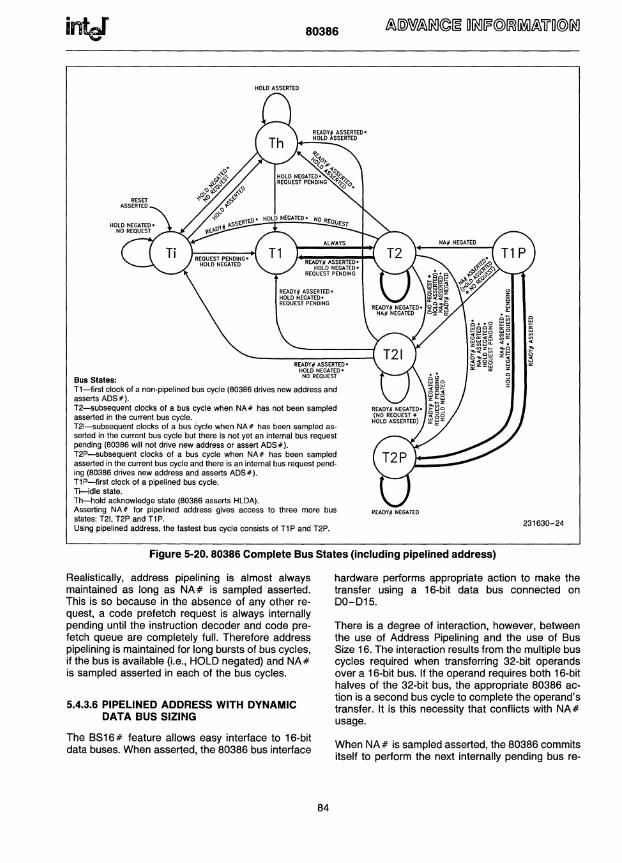
Bus States:
RESET ASSERTED
80386
HOLD ASSERTED
READY# ASSERTEDHOLD NEGATED
NO REQUEST
T1-first clock of a non·pipelined bus cycle (80386 drives new address and asserts ADS #). T2-subsequent clocks of a bus cycle when NA # has not been sampled asserted in the current bus cycle. T21-subsequent clocks of a bus cycle when NA # has been sampled as· serted in the current bus cycle but there is not yet an internal bus request pending (80386 will not drive new address or assert ADS#). T2P-subsequent clocks of a bus cycle when NA # has been sampled asserted in the current bus cycle and there is an internal bus request pend· ing (80386 drives new address and asserts ADS#). T1 P-first clock of a pipelined bus cycle. Ti-idle state. Th-hold acknowledge state (80386 asserts HLDA). Asserting NA # for pipelined address gives access to three more bus states: T21, T2P and T1 P. Using pipe lined address, the fastest bus cycle consists of T1 P and T2P.
READY# NEGATED
Figure 5-20. 80386 Complete Bus States (including pipelined address)
" z
" ~ . ~ " ,,~
~~
ffi ~8 ~~ ~ <. ~"
~ <~
z!< ~ 9 'E
231630-24
Realistically, address pipelining is almost always maintained as long as NA# is sampled asserted. This is so because in the absence of any other request, a code prefetch request is always internally pending until the instruction decoder and code prefetch queue are completely full. Therefore address pipelining is maintained for long bursts of bus cycles, if the bus is available (i.e., HOLD negated) and NA# is sampled asserted in each of the bus cycles.
hardware performs appropriate action to make the transfer using a 16-bit data bus connected on 00-015.
5.4.3.6 PIPElINED ADDRESS WITH DYNAMIC DATA BUS SIZING
The BS 16 # feature allows easy interface to 16-bit data buses. When asserted, the 80386 bus interface
84
There is a degree of interaction, however, between the use of Address Pipelining and the use of Bus Size 16. The interaction results from the multiple bus cycles required when transferring 32-bit operands over a 16-bit bus. If the operand requires both 16-bit halves of the 32-bit bus, the appropriate 80386 action is a second bus cycle to complete the operand's transfer. It is this necessity that conflicts with NA# usage.
When NA# is sampled asserted, the 80386 commits itself to perform the next internally pending bus re-

intJ 80386
quest, and is allowed to drive the next internally pending address onto the bus. Asserting NA # therefore makes it impossible for the next bus cycle to again access the current address on A2-A31, such as may be required when B8 16 # is asserted by the external hardware.
been sampled asserted in the current cycle. If NA# is sampled asserted, the current data bus size is assumed to be 32 bits.
2) To also avoid conflict, if NA# and B816# are both asserted during the same sampling window, B816# asserted has priority and the 80386 acts as if NA# was negated at that time. Internal 80386 circuitry, shown conceptually in Figure 5-18, assures that B816# is sampled asserted and NA# is sampled negated if both inputs are externally asserted at the same sampling window.
To avoid conflict, the 80386 is designed with following two provisions:
1) To avoid conflict, the 80386 is deSigned to ignore B816# in the current bus cycle if NA# has already
CLK2[
(82384 CLK) [
BEO#, BE1# [
BE2#, BE3#, [ A2, A31,
M/IO#,D/C#
W/R#[
ADS#[
READY# [
LOCK# [
DO-D1S[
PREVIOUS CYCLE
T2P
Jl.Jl -V
TIP
ilJl V
A TRANSFER REQUIRING TWO CYCLES ON 16-BIT BUS
PIPELINED NON-PIPELINED CYCLE I~YCLE lA
(WRITE WRITE) PART ONE PART TWO
T2 T2 T1 T2 T2
ilJl rtIl rtIl rtIl rm V \f \f V V
ALWAYS
CYCLE 2 NON-PIPELINED
(READ)
Tl T2 T2P
rm ilJl rtIl V V \f
:~ VALID 1 /NEGATED DURING rx VALID 2 X VALID 3 PART TWO
I -X VALID 1 X VALID 2 X VALID 3 -
_/ \
-'--- -/ '---V \......../ '---{C NOTE: NA# MUST BE NEGATED IN THESE T'S TO ALLOW RECOGNITION OF ASSERTED BSI6# IN FINAL T2'5.
/XXXX'Y ~ (j '< X DON'T CAR~<X ~ '<x:~ ~X ~~)lK<X~ /.. 'X'X"X"X 32-81T
BUStSIZE
XXXXX IXXXX IXXXXI>.. /.. D<XXX IXXX)(>.. ~ XXXXIY '(IXXXX ~
16-BIT 16-BIT BUS SIZE BUS SIZE
'5<500.- -<XX IXXY ~ /..X)( IXXY ~ -<XX IXXY ~
VALID 1 X VALID 2
dO-dIS dO-dIS d16-d31 dO-dl
. ---@-{ OUT OUT - ---- --<m 5
d16-d31 d16-d31 dl6-d 31
Dt6-D31 [ . ---~-{ OUT }- - --- --~ I I
Key: On ~ physical data pin n 231630-25 dn ~ logical data bit n
Cycles 1 and 2 are pipelined. Cycle 1 a cannot be pipe lined, but its address can be inferred from that of Cycle 1, to externally sirnulate address pipelining during Cycle 1 a.
Figure 5·21. Using NA# and 8516#
85

inter 80386
Certain types of 16-bit or 8-bit operands require no adjustment for correct transfer on a 16-bit bus. Those are read or write operands using only the lower half of the data bus, and write operands using only the upper half of the bus since the 80386 simultaneously duplicates the write data on the lower half of the data bus. For these patterns of Byte Enables and the R/W# signals, B816# need not be asserted at the 80386, allowing NA# to be asserted during the bus cycle if desired.
5.4.4 Interrupt Acknowledge (INTA) Cycles
In response to an interrupt request on the INTR input when interrupts are enabled, the 80386 performs
PREVIOUS I CYCLE
T2 TI
INTERRUPT ACKNOWLEDGE
CYCLE 1
T2 T2 T1
two interrupt acknowledge cycles. These bus cycles are similar to read cycles in that bus definition signals define the type of bus activity taking place, and each cycle continues until acknowledged by READY # sampled asserted.
The state of A2 distinguishes the first and second interrupt acknowledge cycles. The byte address driven during the first interrupt acknowledge cycle is 4 (A31-A3 low, A2 high, BE3 # -BE1 # high, and BEO# low). The address driven during the second interrupt acknowledge cycle is 0 (A31-A2 low, BE3#-BE1 # high, BEO# low).
IDLE (4 BUS STATES)
T1 Ti Ti TI
INTERRUPT ACKNOWLEDGE
CYCLE 2
T2 T21
IDLE
TI
ClK2 [ -rut rut rm.. nJ1. rut rut rt.rL nJ1. rut nJ1. nJ1. nJ1. (82384 ClK) [
BEl #. BE2#. BE3# [
BEO#. A3-A31. [ M/ro#. O/C#. W/R#
lOCK# [
AOS#[
BS16# [
READY#[
08-031 [
-V V V V V V V IXXX IY I,{XX IX X XJ\ ,,"XXX
~ XIXXXXi>.. :XX IXXX xx
.XX IY I,{XXX IXXX xx
XIXXXXIi>..
1\--/ xx IXXX.Xl X IXXX XXX XX
IXXX xXX XX IGNORED )(IXXXX XXXX Xx
IXXX .xxx XX'Y ~\ AAJ, XXX .XX IGNORED
... ---- ----- ----- --{I)-- ---- -----IGNORED
... ---- ---- -----~--cp--- ----- -----
V .XX
.XX
XX
xX'X
xX
.XX
-----
-----
Interrupt Vector (0-255) is read on DO-D7 at end of second Interrupt Acknowledge bus cycle.
V V V V 'I' .XX .XX
r I" XX xx
/ I" I<XXX XXXX
/' ~
1\--/ XXXX>.. XX XX
x.xxxr ,<IGNORE~) lXXXX
XXX .XT '\\\ ;:xx VECTOR
--.-. ---- --@---IGNORED
----- ~---- --cp---231630-26
Because each Interrupt Acknowledge bus cycle is followed by idle bus states. asserting NA # has no practical effect. Choose the approach which is simplest for your system hardware design.
Figure 5-22. Interrupt Acknowledge Cycles
86
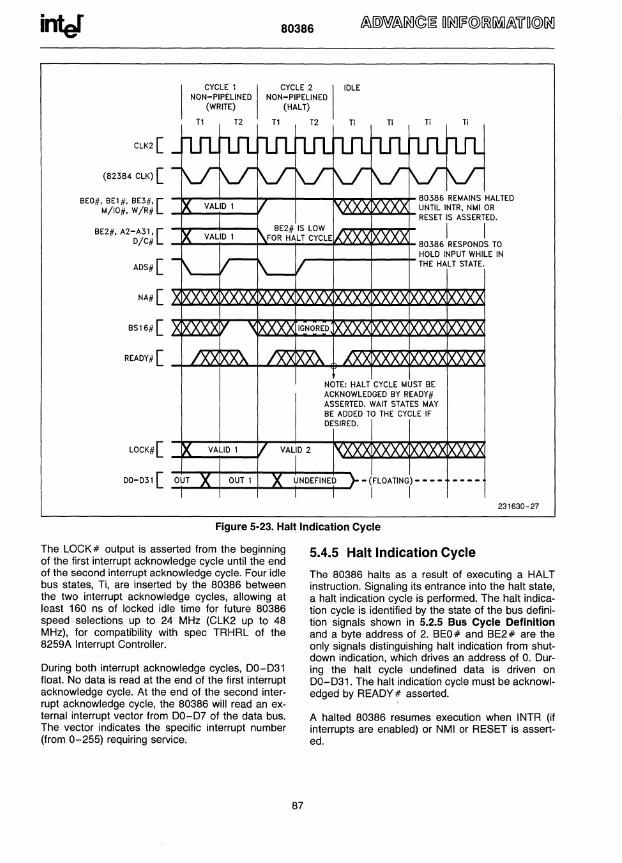
inter 80386
CYCLE 1 I NON-PIPELINED
(WRITE)
T1 T2
CYCLE 2 I NON-PIPELINED
(HALT)
T1 T2
IDLE
Ti Ti Ti Ti
CLK2 [
(82384 CLK) [
BEO~ BEl" BE3"[ MilO" W/R#
'rr-:":,~:-:--+:,-+---bV'\.ml::7o;",,od- 80386 REMAINS HAL TED UNTIL INTR, NMI OR
~"-lo"-..lj'-l"-lo"-~t- RESET IS ASSERTED.
I I BE2#, A2-A31, [ O/C# """,",,~-""'i"'--+a;..;..;....;,,;+...;.;..;;,.;,;;f->'~~f->"~"-t- 80386 RESPONDS TO
ADS#[
NA#[
READY# [
LOCK#[
00-031 [
, ---i---t---t- HOLD INPUT WHILE IN THE HALT STATE.
- (FLOATING) - - --
I I 231630-27
Figure 5-23. Halt Indication Cycle
The LOCK # output is asserted from the beginning of the first interrupt acknowledge cycle until the end of the second interrupt acknowledge cycle. Four idle bus states, Ti, are inserted by the 80386 between the two interrupt acknowledge cycles, allowing at least 160 ns of locked idle time for future 80386 speed selections up to 24 MHz (CLK2 up to 48 MHz), for compatibility with spec TRHRL of the 8259A Interrupt Controller.
During both interrupt acknowledge cycles, 00-031 float. No data is read at the end of the first interrupt acknowledge cycle. At the end of the second interrupt acknowledge cycle, the 80386 will read an external interrupt vector from 00-07 of the data bus. The vector indicates the specific interrupt number (from 0-255) requiring service.
87
5.4.5 Halt Indication Cycle
The 80386 halts as a result of executing a HALT instruction. Signaling its entrance into the halt state, a halt indication cycle is performed. The halt indication cycle is identified by the state of the bus definition signals shown in 5.2.5 Bus Cycle Definition and a byte address of 2. BEO# and BE2# are the only signals distinguishing halt indication from shutdown indication, which drives an address of O. During the halt cycle undefined data is driven on 00-031. The halt indication cycle must be acknowledged by READY # asserted.
A halted 80386 resumes execution when INTR (if interrupts are enabled) or NMI or RESET is asserted.
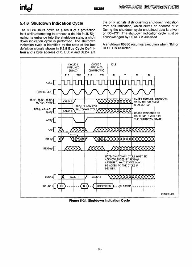
intJ 80386
5.4.6 Shutdown Indication Cycle the only signals distinguishing shutdown indication from halt indication. which drives an address of 2. During the shutdown cycle undefined data is driven on 00-031. The shutdown indication cycle must be acknowledged by READY # asserted.
The 80386 shuts down as a result of a protection fault while attempting to process a double fault. Signaling its entrance into the shutdown state. a shutdown indication cycle is performed. The shutdown indication cycle is identified by the state of the bus definition signals shown in 5.2.5 Bus Cycle Definition and a byte address of O. BEO# and BE2# are
A shutdown 80386 resumes execution when NMI or RESET is asserted.
ClK2[
(82384 ClK) [
BEl #. BE2#. BE3#. [ M/IO#. W/R#
BEO#. A2-A31. [ O/C#
ADS#[
NA#[
READY# [
lOCK#[
00-031 [
CYCLE 1 PIPELINED
(READ)
T1 P T2P
CYCLE 2 PIPELINED
(SHUTDOWN)
T1 P T21
I IDLE
Ti Ti Ti Ti
~---+.,....-+---r,.~~ir-7'I:~d~~~ 80386 REMAINS SHUTDOWN 'Clt/.::.J.~ID.~~t/.::.J.~*- UNTil NMI OR RESET - IS ASSERTED •
• /'V'I:'?~~~~ I ~~~~~-~--~~~~~~~~~80386RESPONOSTO
~-+---l---!---+ HOLD INPUT WHilE IN THE SHUTDOWN STATE.
231630-28
Figure 5-24. Shutdown Indication Cycle
88

80386
5.5 OTHER FUNCTIONAL DESCRIPTIONS
5.5.1 Entering and Exiting Hold Acknowledge
The bus hold acknowledge state, Th, is entered in response to the HOLD input being asserted. In the bus hold acknowledge state, the 80386 floats all output or bidirectional signals, except for HLDA. HLDA is asserted as long as the 80386 remains in the bus hold acknowledge state. In the bus hold acknowledge state, all inputs except HOLD and RESET are ignored (also up to one rising edge on NMI is remembered for processing when HOLD is no longer asserted).
r ACK~g~~EDGE~ 10LE
n Th Th Th n
10LE
(82384 CLK>[
8EO#-8E3# [ A2-A31. M/IO# L~~~
o/c#. w/R# -
AOS#[
LOCK#[ ~~:.cJ( ---- (FLOATING)·---
I (FLOATING)
---------------~----00-031[.
231630-29 NOTE: For maximum design flexibility the 80386 has no internal pullup resistors on its outputs. Your design may require an external PUIIUP on ADS # and other 80386 outputs to keep them negated during float periods.
Figure 5-25. Requesting Hold from Idle Bus
Th may be entered from a bus idle state as in Figure 5-25 or after the acknowledgement of the current physical bus cycle if the LOCK# signal is not asserted, as in Figures 5-26 and 5-27. If asserting BS16# requires a second 16-bit bus cycle to complete a physical operand transfer, it is performed before
89
HOLD is acknowledged, although the bus state diagrams in Figures 5-13 and 5-20 do not indicate that detail.
Th is exited in response to the HOLD input being negated. The following state will be Ti as in Figure 5-25 if no bus request is pending. The following bus state will be T1 if a bus request is internally pending, as in Figures 5-26 and 5-27.
Th is also exited in response to RESET being asserted.
If a rising edge occurs on the edge-triggered NMI input while in Th, the event is remembered as a nonmaskable interrupt 2 and is serviced when Th is exited, unless of course, the 80386 is reset before Th is exited.
5.5.2 Reset During Hold Acknowledge
RESET being asserted takes priority over HOLD being asserted. Therefore, Th is exited in reponse to the RESET input being asserted. If RESET is asserted while HOLD remains asserted, the 80386 drives its pins to defined states during reset, as in Table 5-3 Pin State During Reset, and performs internal reset activity as usual.
If HOLD remains asserted when RESET is negated, the 80386 enters the hold acknowledge state before performing its first bus cycle, provided HOLD is still asserted when the 80386 would otherwise perform its first bus cycle. If HOLD remains asserted when RESET is negated, the BUSY # input is still sampled as usual to determine whether a self test is being requested, and ERROR# is still sampled as usual to determine whether an 80387 vs. an 80287 (or none) is present.
5.5.3 Bus Activity During and Following Reset
RESET is the highest priority input signal, capable of interrupting any processor activity when it is asserted. A bus cycle in progress can be aborted at any stage, or idle states or bus hold acknowledge states discontinued so that the reset state is established.
RESET should remain asserted for at least 15 CLK2 periods to ensure it is recognized throughout the 80386, and at least 78 CLK2 periods if 80386 selftest is going to be requested at the falling edge. RESET asserted pulses less than 15 CLK2 periods may not be recognized. RESET pulses less than 78 CLK2 periods followed by a self-test may cause the selftest to report a failure when no true failure exists. The additional RESET pulse width is required to clear additional state prior to a valid self-test.
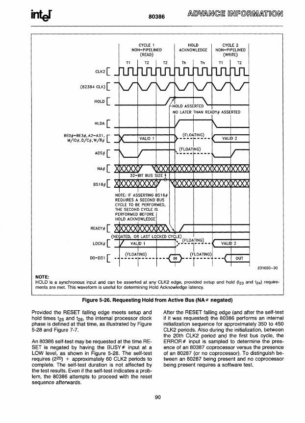
inter 80386
NOTE:
CLK2[
(82384 ClK) [
HOLD [
HLDA [
BEO#-BE3#, A2-A31, [ M/IO#, D/C#, W /R#
ADS# [
T1
CYCLE 1 NON-PIPELINED
(READ)
T2 T2
NOTE: IF ASSERTING BS 16# REQUIRES A SECOND BUS CYCLE TO BE PERFORMED, THE SECOND CYCLE IS PERFORMED BEFORE HOLD ACKNOWLEDGE
HOLD CYCLE 2 ACKNOWLEDGE NON-PIPELINED
(WRITE)
Th Th T1 T2
VALID 2
OUT
231630-30
HOLD is a synchronous input and can be asserted at any CLK2 edge, provided setup and hold (t23 and t24) requirements are met. This waveform is useful for determining Hold Acknowledge latency.
Figure 5-26. Requesting Hold from Active Bus (NA # negated)
Provided the RESET falling edge meets setup and hold times t25 and t26, the internal processor clock phase is defined at that time, as illustrated by Figure 5-28 and Figure 7-7.
An 80386 self-test may be requested at the time RESET is negated by having the BUSY # input at a LOW level, as shown in Figure 5-28. The self-test requires (220) + approximately 60 CLK2 periods to complete. The self-test duration is not affected by the test results. Even if the self-test indicates a problem, the 80386 attempts to proceed with the reset sequence afterwards.
90
After the RESET falling edge (and after the self-test if it was requested) the 80386 performs an internal initialization sequence for approximately 350 to 450 CLK2 periods. Also during the initialization, between the 20th CLK2 period and the first bus cycle, the ERROR # input is sampled to determine the presence of an 80387 coprocessor versus the presence of an 80287 (or no coprocessor). To distinguish between an 80287 being present and no coprocessor being present requires a software test.
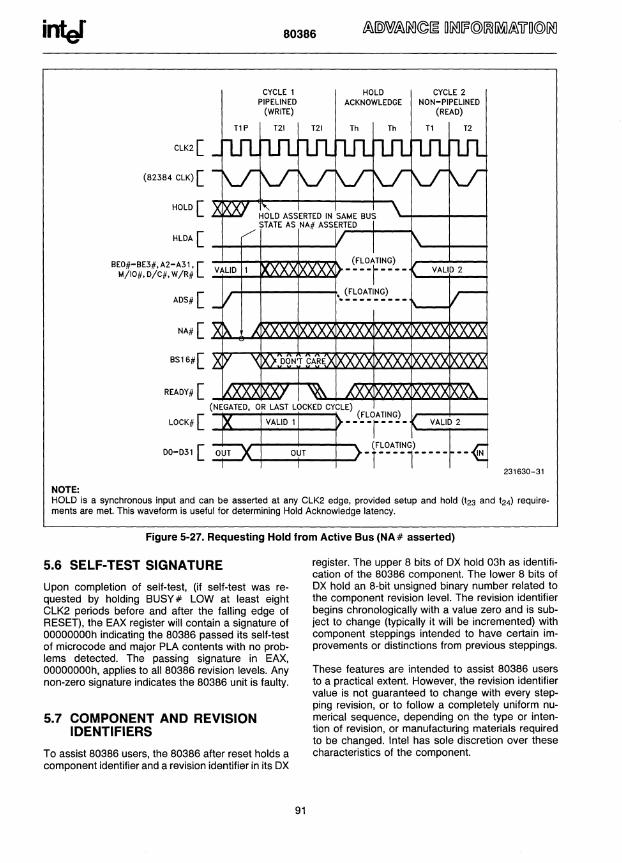
intJ 80386
CLK2[
(82384 CLK) [
HOLD [
HLDA [
8EO#-8E3#, A2-A31, [ M/IO#, D/c#, W/R#
ADS# [
TIP
CYCLE 1 PIPELINED
(WRITE)
T21 T21
HOLD CYCLE 2 ACKNOWLEDGE NON-PIPELINED
(READ)
Th Th TI T2
NA# [ ..Qja~-4~~~~~~~~~~~~
231630-31
NOTE: HOLD is a synchronous input and can be asserted at any CLK2 edge, provided setup and hold (t23 and t24) requirements are met. This waveform is useful for determining Hold Acknowledge latency.
Figure 5-27. Requesting Hold from Active Bus (NA # asserted)
5.6 SELF-TEST SIGNATURE
Upon completion of self-test, (if self-test was requested by holding BUSY # LOW at least eight CLK2 periods before and after the falling edge of RESET), the EAX register will contain a signature of OOOOOOOOh indicating the 80386 passed its self-test of microcode and major PLA contents with no problems detected. The passing signature in EAX, OOOOOOOOh, applies to all 80386 revision levels. Any non-zero signature indicates the 80386 unit is faulty.
5.7 COMPONENT AND REVISION IDENTIFIERS
To assist 80386 users, the 80386 after reset holds a component identifier and a revision identifier in its OX
91
register. The upper 8 bits of OX hold 03h as identification of the 80386 component. The lower 8 bits of OX hold an 8-bit unsigned binary number related to the component revision level. The revision identifier begins chronologically with a value zero and is subject to change (typically it will be incremented) with component steppings intended to have certain improvements or distinctions from previous step pings.
These features are intended to assist 80386 users to a practical extent. However, the revision identifier value is not guaranteed to change with every stepping revision, or to follow a completely uniform numerical sequence, depending on the type or intention of revision, or manufacturing materials required to be changed. Intel has sole discretion over these characteristics of the component.
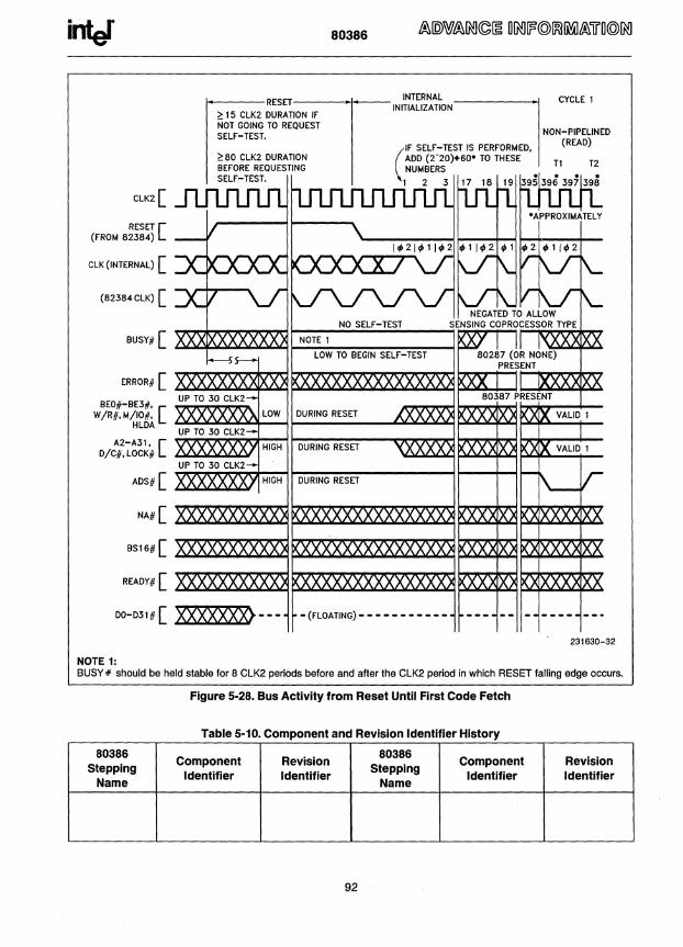
intJ 80386
INTERNAL I----RESET----I---INITIALIZATION-----+l
ClK2[
RESET [ (FROM 82384)
ClK (INTERNAL) [
(82384ClK) [
9USY# [
ERROR# [
9EO#-9E3#. W/R#.M/IO#. [
HlDA
~ 15 ClK2 DURATION IF NOT GOING TO REQUEST SELF-TEST.
DURING RESET
A2-A31. [ D/C#. lOCK# ~~_~_ DURING RESET
ADS#[ ~~~~ DURING RESET
CYCLE 1
NON-PIPELINED (READ)
T1 T2
NA#[ ~~~~~~~~~~~~I.CI~~~~~~~
READY#[
00-031 # [ XXXXXXX> --- -(FLOATING) - - - - - - - - - --
231630-32
NOTE 1: BUSY # should be held stable for B CLK2 periods before and after the CLK2 period in which RESET falling edge occurs.
Figure 5-28. Bus Activity from Reset Until First Code Fetch
Table 5-10. Component and Revision Identifier History
80386 Component Revision
80386 Component Revision
Stepping Stepping Name
Identifier Identifier Name
Identifier Identifier
92

inter 80386
5.8 COPROCESSOR INTERFACING
The 80386 provides an automatic interface for the Intel 80287 or 80387 numeric floating-point coprocessors. The 80287 and 80387 coprocessors use an I/O-mapped interface driven automatically by the 80386 and assisted by three dedicated signals: BUSY #, ERROR #, and PEREa.
As the 80386 begins supporting a coprocessor instruction, it tests the BUSY # and ERROR # signals to determine if the coprocessor can accept its next instruction. Thus, the BUSY # and ERROR # inputs eliminate the need for any "preamble" bus cycles for communication between processor and coprocessor. The 80287 and 80387 can be given its command opcode immediately. The dedicated signals provide instruction synchronization, and eliminate the need of using the 80386 WAIT opcode (9Bh) for 80287/80387 instruction synchronization (the WAIT opcode was required when 8086 or 8088 was used with the 8087 coprocessor).
Custom coprocessors can be included in 80386-based systems, via memory-mapped or I/O-mapped interfaces. Such coprocessor interfaces allow a completely custom protocol, and are not limited to a set of coprocessor protocol "primitives". Instead, memory-mapped or I/O-mapped interfaces may use all applicable 80386 instructions for high-speed coprocessor communication. The BUSY # and ERROR # inputs of the 80386 may also be used for the custom coprocessor interface, if such hardware assist is desired. These signals can be tested by the 80386 WAIT opcode (9Bh). The WAIT instruction will wait until the BUSY # input is negated (interruptable by an NMI or enabled INTR input), but generates an exception 16 fault if the ERROR # pin is in the asserted state when the BUSY # goes (or is) negated. If the custom coprocessor interface is memory-mapped, protection of the addresses used for the interface can be provided with the 80386 onchip paging or segmentation mechanisms. If the custom interface is I/O-mapped, protection of the interface can be provided with the 80386 10PL (I/O Privilege Level) mechanism.
The 80287 and 80387 numeric coprocessor interfaces are I/O mapped as shown in Table 5-11. Note that the 80287/80387 coprocessor interface addresses are beyond the Oh-FFFFh range for programmed I/O. When the 80386 supports the 80287 or 80387 coprocessors, the 80386 automatically generates bus cycles to the coprocessor interface addresses.
93
Table 5·11. Numeric Coprocessor Port Addresses
Address in 80287 80387 80386 Coprocessor Coprocessor
I/O Space Register Register
800000F8h Opcode Register Opcode Register (16-bit port) (32-bit port)
800000FCh Operand Register Operand Register (16-bit port) (32-bit port)
The 80287 coprocessor (16-bit) functions with either 80286 or 80386 processor. The 80387 coprocessor (32-bit) functions with the 80386 processor. To correctly map the 80287 and 80387 registers to the appropriate I/O addresses, connect the CMDO and CMD1 lines of the 80287/80387 as listed in Table 5-12.
Table 5·12. Connections for CMDO and CMD1 Inputs of 80287180387
Coprocessor Coprocessor Coprocessor and Processor CMDO CMD1 Configuration Connection Connection
80387 connected connect to None-80387 to 80386 latched version has no CMD1
of '386 A2 signal pin
80287 connected connect to connect to to 80386 latched version ground
of '386 A2 signal
80287 connected connect to connect to to 80286 latched version latched version
of '286 A 1 signal of '286 A2 signal
5.8.1 Software Testing for Coprocessor Presence
When software is used to test for coprocessor (80387 or 80287) presence, it should use only the following coprocessor opcodes: FIN IT, FNINIT, FSTCW mem, FSTSW mem, FSTSW AX. To use other coprocessor opcodes when a coprocessor is known to be not present, first set EM = 1 in 80386 CRO.
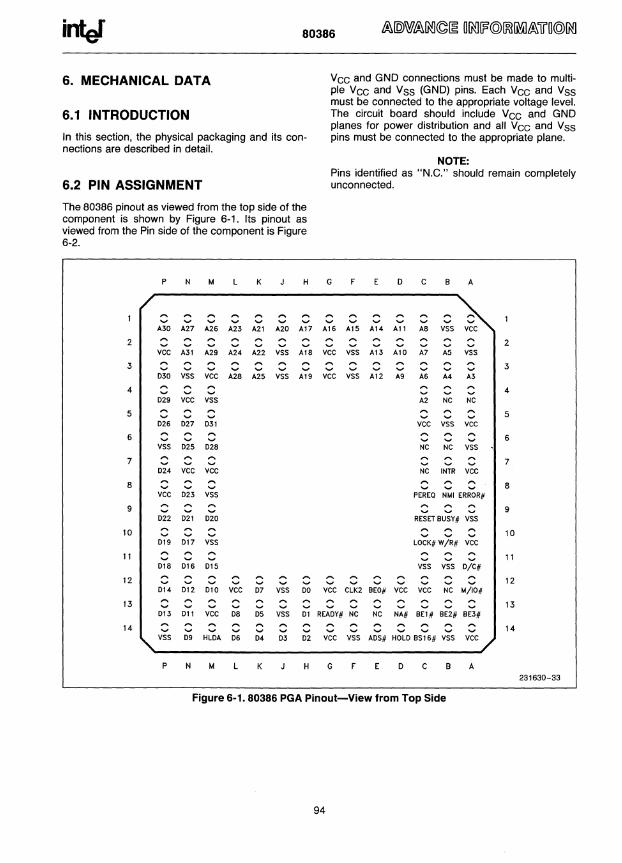
inter 80386 ~[Q)W~OO~[g OOOIP@OO~~lf'O@OO
6. MECHANICAL DATA vee and GND connections must be made to multi-ple Vee and Vss (GND) pins. Each Vee and Vss must be connected to the appropriate voltage level.
6.1 INTRODUCTION The circuit board should include Vee and GND planes for power distribution and all Vee and Vss
In this section, the physical packaging and its con- pins must be connected to the appropriate plane. nections are described in detail.
NOTE: Pins identified as "N.C." should remain completely
6.2 PIN ASSIGNMENT unconnected.
The 80386 pinout as viewed from the top side of the component is shown by Figure 6-1. Its pinout as viewed from the Pin side of the component is Figure 6-2.
p N M L K H G D C B A
A30 A27 A26 A23 A21 A20 A17 A16 A15 A14 All A8 VSS vee 2 .... .... 2
vec A31 A29 A24 A22 VSS AlB vee VSS A13 Al0 A7 A5 VSS
3 3 030 VSS vec A28 A25 VSS A19 vee VSS A12 A9 A6 A4 A3
4 4 029 vee VSS A2 NC Ne
5 5 026 027 031 vee VSS vce
6 6 VSS 025 028 NC Ne VSS
7 7 024 VCC vec NC INTR vce
8 8 vcc 023 VSS PEREQ NMI ERROR#
9 ~ ~
9 .... .... 022 021 020 RESET 8USY# VSS
10 10 019 017 VSS LOCK# W/R# VCC
11 11 018 016 015 VSS VSS o/c#
12 ~ ~ ~ ~ ~ ~ ~ 12 .... .... .... .... .... .... .... 014 012 010 vec 07 VSS 00 vec CLK2 8EO# vcc vce NC M/IO#
13 13 013 011 VCC 08 05 VSS 01 REAOY# Ne NC NA# 8El# 8E2# 8E3#
14 14 VSS 09 HLOA 06 04 03 02 VCC VSS AOS# HOLO 8S16# VSS vcc
P N M L K H G E D C B A
231630-33
Figure 6-1. 80386 PGA Pinout-View from Top Side
94

inter 80386
A B c D E F G H K L N p
o 0 000 0 0 0 000 0 0 0 vee vss A8 All A14 A15 A16 A17 A20 A21 A23 A26 A27 A30
2 o 0 000 0 0 0 0 000 0 0 2 VSS A5 A7 Al0 A13 VSS vee A18 VSS A22 A24 A29 A31 vee
3 o 0 0 0 0 0 0 0 0 0 0 000 3 A3 A4 A6 A9 A12 VSS vee A19 VSS A25 A28 vee VSS D30
4 000 000 4 Ne Ne A2 vss vee D29
5 000 000 5 vee vss vee
METAL LID D31 D27 D26
6 000 000 6 vss Ne Ne D28 D25 VSS
7 000 000 7 vee INTR Ne vee vee D24
8 000 000 8 ERROR# NMI PEREQ VSS D23 vee
9 000 000 9 vss BUSY# RESET D20 D21 D22
10 000 000 10 vee W/R# LoeK# vss D17 019
11 00000 0 11 D/e# vss vss D15 D16 D18
12 o 000 0 0 0 0 0 0 0 0 0 0 12 M/IO# Ne vee vee BEO# eLK2 vee DO VSS D7 vee Dl0 D12 D14
13 o 0 0 0 0 0 0 0 0 0 0 0 0 0 13 BE3# BE2# BEl # NA# Ne Ne READY# Dl VSS D5 D8 vee Dll D13
14 o 0 0 0 0 0 0 000 000 0 14 vee vss BS16# HOLD ADS# vss vee D2 D3 D4 D6 HLDA D9 VSS
A B c D E F G H K L N p 231630-34
Figure 6·2. 80386 PGA Pinout-View from Pin Side
95
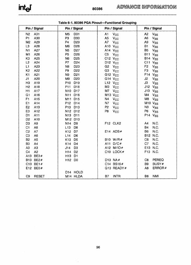
intJ 80386
Table 6-1. 80386 PGA Pinout-Functional Grouping
Pin /Signal Pin/ Signal Pin/Signal Pin/Signal
N2 A31 M5 031 A1 Vee A2 Vss P1 A30 P3 030 A5 Vee A6 Vss M2 A29 P4 029 A7 Vee A9 Vss L3 A28 M6 028 A10 Vee 81 Vss N1 A27 N5 027 A14 Vee 85 Vss M1 A26 P5 026 C5 Vee 811 Vss K3 A25 N6 025 C12 Vee 814 Vss L2 A24 P7 024 012 Vee C11 Vss L1 A23 N8 023 G2 Vee F2 Vss K2 A22 P9 022 G3 Vee F3 Vss K1 A21 N9 021 G12 Vee F14 Vss J1 A20 M9 020 G14 Vee J2 Vss H3 A19 P10 019 L12 Vee J3 Vss H2 A18 P11 018 M3 Vee J12 Vss H1 A17 N10 017 M7 Vee J13 Vss G1 A16 N11 016 M13 Vee M4 Vss F1 A15 M11 015 N4 Vee M8 Vss E1 A14 P12 014 N7 Vee M10 Vss E2 A13 P13 013 P2 Vee N3 Vss E3 A12 N12 012 P8 Vee P6 Vss 01 A11 N13 011 P14 Vss 02 A10 M12 010 03 A9 N14 09 F12 CLK2 A4 N.C. C1 A8 L13 08 84 N.C. C2 A7 K12 07 E14 AOS# 86 N.C. C3 A6 L14 06 812 N.C. B2 A5 K13 05 B10 W/R# C6 N.C. B3 A4 K14 04 A11 O/C# C7 N.C. A3 A3 J14 03 A12 MIIO# E13 N.C. C4 A2 H14 02 C10 LOCK# F13 N.C. A13 BE3# H13 01 B13 BE2# H12 DO 013 NA# C8 PEREQ C13 8E1# C14 BS16# B9 BUSY# E12 BEO# G13 REAOY# A8 ERROR#
014 HOLD C9 RESET M14 HLOA B7 INTR B8 NMI
96

inter 80386
0;- r:- ~ ;;;- N 0;- r:-
"' "' '" <J) 0 ... OJ '\ '" ... ~ OJ I') OJ .,; .,; C ~ e e c c c
C IN #l POSITION
2
3
4
5
6
7
• ®00®00'10000000 ®00®0000000000 o ® ~ 0 0 ® ®'0 0 0 0 ~ 0 0 000 00® ®®0 ®00 0®0 I ®00 0®0 + 00®
B -0 0 @ -- - - ® 0 ® 9
10
11
12
13
14
00® 0®0 0®® 0®® ®®0 000 o ® e 0000,0000 00 o ® ® 0 ® 0 010 ® 0@0 0 0 ® ® ® 0 ® ® ®,®@@@@®®
0 ... <Xi c L()
'" r-:
M .O~O ':....1_ ABC D E F G H J K L .020 (0.508) MIN TYP
- .070 (1.777) DIA TYP BRAZE PAD
(0.508)
1------ 1.450 (36.802) -------1
.725 (18.401)
.650 (16.497)
.550 (13.959)
.450 (11.421)
.350 (8.883)
.250 (6.345)
.150 (3.807)
.050 (1.269) o
SWEDGE PIN STANDOFF (4) PLACES
.057(1.269) -11-
MAX TYP
.001 (0.025) R
MIN TYP
.018 (0.47) 1 DIA TYP - =~1If
.165(4'189~1 ~ .110(2:J-j
231630-35
Figure 6-3. 132-Pin Ceramic PGA Package Dimensions
6.3 Package Dimensions and Mounting
The initial 80386 package is a 132-pin ceramic pin grid array (PGA). Pins of this package are arranged 0.100 inch (2.54mm) center·to·center, in a 14 x 14 matrix, three rows around.
97
A wide variety of available sockets allow low insertion force or zero insertion force mountings, and a choice of terminals such as soldertail, surface mount, or wire wrap. Several applicable sockets are listed in Table 6·2.
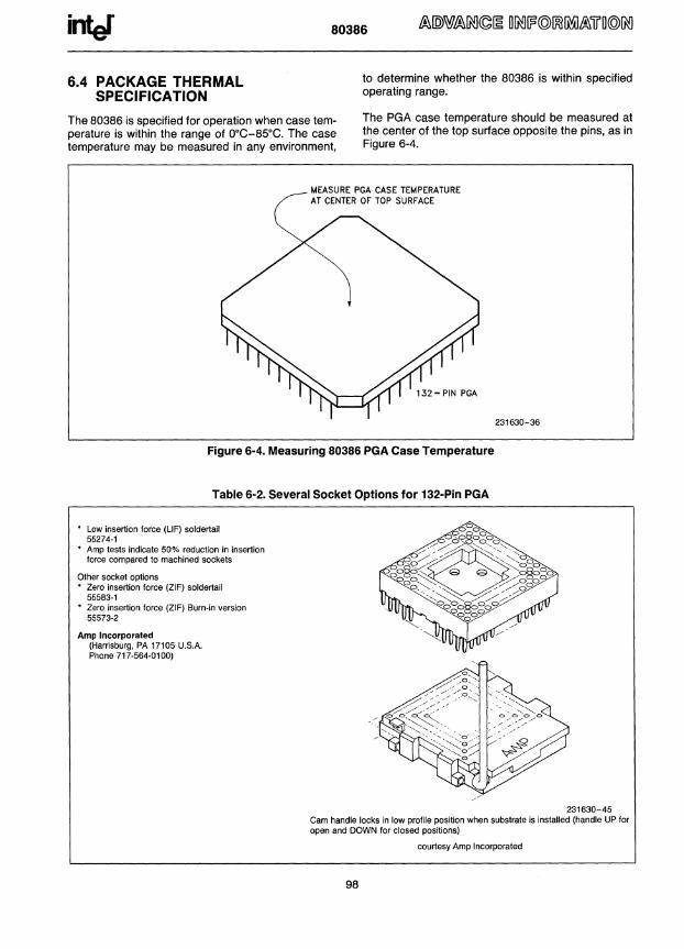
inter 6.4 PACKAGE THERMAL
SPECIFICATION
80386
to determine whether the 80386 is within specified operating range.
The 80386 is specified for operation when case temperature is within the range of 0°C-85°C. The case temperature may be measured in any environment,
The PGA case temperature should be measured at the center of the top surface opposite the pins, as in Figure 6-4.
MEASURE PGA CASE TEMPERATURE AT CENTER Of TOP SURfACE
231630-36
Figure 6·4. Measuring 80386 PGA Case Temperature
Table 6-2. Several Socket Options for 132-Pin PGA
• Low insertion force (LlF) soldertail 55274·1
• Amp tests indicate 50% reduction in insertion force compared to machined sockets
Other socket options • Zero insertion force (ZIF) soldertail
55583·1 • Zero insertion force (ZIF) Burn·in version
55573-2
Amp Incorporated (Harrisburg, PA 17105 U.S.A. Phone 717·564-0100)
231630-45 Cam handle locks in low profile position when substrate is installed (handle UP for open and DOWN for closed positions)
courtesy Amp Incorporated
98
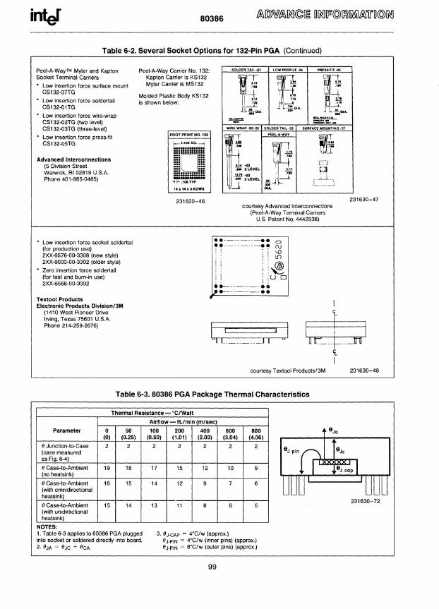
infef 80386
Table 6-2. Several Socket Options for 132-Pin PGA (Continued)
Peel-A-WayTM Mylar and Kapton Socket Terminal Carriers
• Low insertion force surface mount CSI32-37TG
Low insertion force soldertail CS132-0tTG
Low insertion force wire-wrap CS132-02TG (two level) CS132-03TG (three-level)
• Low insertion force press-fit CS132-05TG
Advanced Interconnections (5 Division Street Warwick, RI 02818 U.S.A. Phone 401-885·0485)
.. Low insertion force socket soldertail (for production use) 2XX-6576-00-3308 (new style) 2XX-6003-00-3302 (older style)
Zero insertion force soldertail (for test and burn-in use) 2XX-6568-00-3302
Textool Products
Peel-A-Way Carrier No. 132: Kapton Carrier is KS132 Mylar Carrier is MS132
Molded Plastic Body KS132 is shown below:
fOOT PRINT NO. 132
~1ii ~Ui~ -i 1-- .100TYP
1411413ROWS
231630-46
SOLDER T~L-01 LOW PROFILE -04 PRESS FIT·05
WIRE WRAP ..02/-03 SOLDER TAll.33 SURFACE MOUNTING -31
PEEL·A·WAY 1-r -:Hi
Y 1.14 -02 :iii 2LEYEL
~-03 .100 3 LEVEL
~= .•... " ., .. '" I -:iii
---.l. ~-I\--~ D'"
courtesy Advanced Interconnections (Peel-A-Way Terminal Carriers
U.S. Patent No. 4442938)
•• - -- -- •• 0
·r-~--~ -~~ (\j
I: ,I ~ il'l: '& " I ~ i i ::U 0 • ~-------l ~ ij------~- ••
I
231630-47
Electronic Products Division/3M (1410 West Pioneer Drive Irving, Texas 75601 U.S.A. Phone 214-259-2676)
I i II wi WI L~ __ ~ __ ~I I ~
Ii. I
courtesy Textool Products/3M 231630-48
Table 6-3. 80386 PGA Package Thermal Characteristics
Thermal Resistance - °C/Watl
Airflow - ft.!min (m/sec)
Parameter 0 50 100 200 400 600 800 °Ja (0) (0.25) (0.50) (1.01) (2.03) (3.04) (4.06)
o Junction-to-Case 2 2 2 2 2 2 2 OJ pin (\ °Jc (case measured
as Fig. 6-4)
I OJ cap 1 o Case-te-Ambient 19 18 17 15 12 10 9 (no heatsink)
UUl UUU o Case-to-Ambient 16 15 14 12 9 7 6 (with omnidirectional heatsink)
o Case-to-Ambient 231630-72
15 14 13 11 8 6 5 (with unidirectional heatsink)
NOTES: 1. Table 6-3 applies to 80386 PGA plugged 3. OJ-CAP ~ 4'C/w (approx.) into socket or soldered directly into board. o J-PIN ~ 4°C/w (inner pins) (approx.) 2. 0JA ~ 0JC + 0CA· OJ.PIN ~ 8°C/w (outer pins) (approx.)
99
inter 80386
7. ELECTRICAL DATA
7.1 INTRODUCTION
The following sections describe recommended electrical connections for the 80386, and its electrical specifications.
7.2 POWER AND GROUNDING
7.2.1 Power Connections
The 80386 is implemented in CHMOS III technology and has modest power requirements. However, its high clock frequency and 72 output buffers (address, data, control, and HLDA) can cause power surges as multiple output buffers drive new signal levels simultaneously. For clean on-chip power distribution at high frequency, 20 Vee and 21 Vss pins separately feed functional units of the 80386.
Power and ground connections must be made to all external Vee and GND pins of the 80386. On the circuit board, all Vee pins must be connected on a Vee plane. All VSS pins must be likewise connected on a GND plane.
7.2.2 Power Decoupling Recommendations
Liberal decoupling capacitance should be placed near the 80386. The 80386 driving its 32-bit parallel address and data buses at high frequencies can cause transient power surges, particularly when driving large capacitive loads.
Low inductance capacitors and interconnects are recommended for best high frequency electrical performance. Inductance can be reduced by shortening circuit board traces between the 80386 and decou-
piing capacitors as much as possible. Capacitors specifically for PGA packages are also commercially available, for the lowest possible inductance.
7.2.3 Resistor Recommendations
The ERROR # and BUSY # inputs have resistor pullups of approximately 20 K!l built-in to the 80386 to keep these signals negated when neither 80287 or 80387 are present in the system (or temporarily removed from its socket). The BS16# input also has an internal pullup resistor of approximately 20 K!l, and the PEREa input has an internal pulldown resistor of approximately 20 K!l.
In typical designs, the external pullup resistors shown in Table 7-1 are recommended. However, a particular design may have reason to adjust the resistor values recommended here, or alter the use of pullup resistors in other ways.
7.2.4 Other Connection Recommendations
For reliable operation, always connect unused inputs to an appropriate signal level. N.C. pins should always remain unconnected.
Particularly when not using interrupts or bus hold, (as when first prototyping, perhaps) prevent any chance of spurious activity by connecting these associated inputs to GND:
Pin Signal
B7 INTR B8 NMI 014 HOLD
If not using address pipelining, pullup 013 NA # to Vee·
If not using 16-bit bus size, pullup C14 BS16# to Vee·
Pullups in the range of 20 K!l are recommended.
Table 7·1. Recommended Resistor Pullups to Vee
Pin and Signal Pullup Value Purpose
E14 ADS# 20 K!l ±10% Lightly Pull ADS# Negated During 80386 Hold Acknowledge States
C10 LOCK # 20 K!l ±10% Lightly Pull LOCK # Negated During 80386 Hold Acknowledge States
100
80386
7.3 MAXIMUM RATINGS
Table 7-2. Maximum Ratings
80386·12 Parameter 80386·16
Maximum Rating
Storage Temperature - 65'C to + 150'C
Case Temperature Under Bias -65'Cto +110'C
Supply Voltage with Respect to Vss - 0.5V to + 6.5V
Voltage on Other Pins -0.5VtoVcc + 0.5V
7.4 D.C. SPECIFICATIONS
Table 7-2 is a stress rating only, and functional operation at the maximums is not guaranteed. Functional operating conditions are given in 7.4 D.C. Specifications and 7.5 A.C. Specifications.
Extended exposure to the Maximum Ratings may affect device reliability. Furthermore, although the B03B6 contains protective circuitry to resist damage from static electric discharge, always take precautions to avoid high static voltages or electric fields.
Functional Operating Range: VCC = 5V ± 5%; TCASE = O°C to 85°C
Table 7-3. 80386-16 and 80386-12 D.C. Characteristics
Symbol Parameter
Input Low Voltage
Input High Voltage
CLK2 Input Low Voltage
CLK2 Input High Voltage
VOL Output Low Voltage IOL = 4 mA: A2-A31,00-031 IOL = 5 mA: BEO#-BE3#, W/R#,
O/C#, MIIO#, LOCK#, AOS#, HLDA
VOH Output High Voltage IOH = -1 mA: A2-A31, 00 IOH = -0.9 mA: BEO#-BE3#,
O/C#, MilO OC
r-____ ~--------------~A HLO III Input Leakage Current (f r
BS16#, PER EO, BUS ERROR#)
ICC
COUT Output or 1/0 Capacitance
CCLK CLK2 Capacitance
NOTES: 1. The min value, -0.3, is not 100% tested. 2. PEREQ input has an internal pulldown resistor.
80386-12 80386-12 80386-16 80386-16 Unl~
Min Max
-0.3 0.8
2.0
-0.3
±15 /LA
200 ).LA
-400 /LA
±15 /LA
400 mA 460 mA
10 pF
12 pF
20 pF
3. BS16#, BUSY# and ERROR# inputs each have an internal pull up resistor. 4. Not 100% tested.
101
Notes
Note 1
Note 1
OV :0: VIN :0: Vcc
VIH = 2.4V (Note 2)
VIL = 0.45V (Note 3)
0.45V :0: VOUT :0: VCC
Icc typo = 300 mA ICC typo = 370 mA
Fc = 1 MHz (Note 4)
Fc = 1 MHz (Note 4)
Fc = 1 MHz (Note 4)
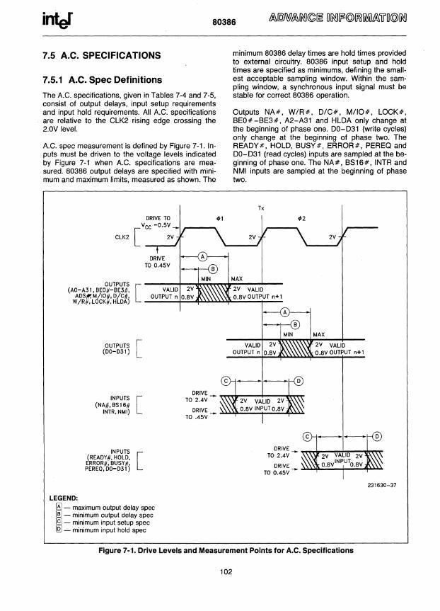
intJ 80386
7.5 A.C. SPECIFICATIONS
7.5.1 A.C. Spec Definitions
The A.C. specifications, given in Tables 7-4 and 7-5, consist of output delays, input setup requirements and input hold requirements. All A.C. specifications are relative to the CLK2 rising edge crossing the 2.0V level.
A.C. spec measurement is defined by Figure 7-1. Inputs must be driven to the voltage levels indicated by Figure 7-1 when A.C. specifications are measured. 80386 output delays are specified with minimum and maximum limits, measured as shown. The
CLK2
minimum 80386 delay times are hold times provided to external circuitry. 80386 input setup and hold times are specified as minimums, defining the smallest acceptable sampling window. Within the sampling window, a synchronous input signal must be stable for correct 80386 operation.
Outputs NA#, W/R#, O/C#, M/IO#, LOCK#, BEO#-BE3#, A2-A31 and HLDA only change at the beginning of phase one. 00-031 (write cycles) only change at the beginning of phase two. The REAOY#, HOLO, BU8Y#, ERROR#, PEREQ and 00-031 (read cycles) inputs are sampled at the beginning of phase one. The NA#, B816#, INTR and NMI inputs are sampled at the beginning of phase two.
Tx
(AO-A31, BEO#-BE3#, VALID OUTPUTS [
ADSt:M/IO#. D/C#. J:\',\\,\\\~ O.BV OUTPUT n+1 W/R#. LOCK#. HLDA) ___ -+;,,;,;,.~ .... ~~to.,;,,;,~_..,.. __
LEGEND:
OUTPUTS [ (DO-D31 )
INPUTS [ (NA#.BS16#
INTR. NMI)
INPUTS (READY#. HOLD. [ ERROR#. BUSY#. PEREa. DO-D31)
; - maximum output delay spec
B _ minimum output delay spec c - minimum input setup spec D _ minimum input hold spec
DRIVE _ ~~---+---m,"" TO 2.4V
DRIVE TO .45V
DRIVE TO 2.4V
DRIVE TO 0.45V
MAX
2V VALID O.BV OUTPUT n+1
Figure 7-1. Drive Levels and Measurement Points for A.C. Specifications
102
231630-37

intJ 80386 ~[Q)W~[RI]~~ OOO[f@OOfMl~'TI'O@OO
7.5.2 A.C. Specification Tables
Functional Operating Range: Vee = 5V ±5%; TeASE = O°C to 85°C
Table 7·4. 80386-16 A.C. Characteristics
Symbol Parameter 80386-16 80386-16
Unit Ref.
Notes Min Max Figure
Operating Frequency 4 16 MHz Half of CLK2 Frequency
t1 CLK2 Period 31 125 ns 7-3
t2a CLK2 High Time 9 ns 7-3 at2V
t2b CLK2 High Time 5 ns 7-3 at (Vee - 0.8V)
t3a CLK2 Low Time 9 ns 7-3 at2V
t3b CLK2 Low Time 7 ns
t4 CLK2 Fall Time 8 ns
t5 CLK2 Rise Time 8 (Vee - 0.8V)
t6 A2-A31 Valid Delay 40 120 pF
t7 A2-A31 Float Delay
t8 BEO#-BE3#, LOCK# Valid Delay
t9 BEO#-BE3#, LOCK# (Note 1) Float Delay
t10 W/R#, M/IO#, O/C#, 4 CL = 75 pF AOS# Valid Delay
t11 W/R#, M/IO#, O/C#, (Note 1) ADS # Float Delay
t12 00-031 Write Data 7-5 CL = 120 pF Valid Delay
t13 ns 7-6 (Note 1)
t14 ns 7-6 CL = 75 pF
t15 NA# ns 7-4
t16 NA# ns 7-4
t17 BSf6# ns 7-4
t18 20 ns 7-4
t19 upTime 20 ns 7-4
t20 READY # Hold Time 3 ns 7-4
t21 00-031 Read 10 ns 7-4 Setup Time
t22 00-031 Read 5 ns 7-4 Hold Time
t23 HOLD Setup Time 25 ns 7-4
t24 HOLD Hold Time 4 ns 7-4
t25 RESET Setup Time 12 ns 7-7
103

inter 80386
Table 7-4. 80386-16 A.C. Characteristics (Continued)
Symbol
NOTES:
Parameter
RESET Hold Time
NMI, INTR Setup Time
NMI, INTR Hold Time
PEREQ,ERROR#,BUSY# Setup Time
PEREQ,ERROR#,BUSY# Hold Time
80386-16 80386-16 Min Max
3
15
15
15
9
1. Float condition occurs when maximum output current becomes less than IL tested. 2. These inputs are aI/owed to be asynchronous to CLK2. The setup and hoi to assure recognition within a specific CLK2 period.
Symbol Parameter Min
Operating Frequency
t1 CLK2 Period
t2a CLK2 High Time
t2b CLK2 High Time
t3a ns
t3b ns
t4 ns
ts 8 ns
t6 45 ns
t7 45 ns
ta 45 ns Valid Delay
tg BEO#-BE3#, LOCK# 45 ns Float Delay
tlO W/R#, M/IO#, D/C#, 4 40 ns ADS# Valid Delay
t11 W/R#, M/IO#, D/C#, 4 40 ns ADS # Float Delay
t12 DO-D31 Write Data 55 ns Valid Delay
t13 DO-D31 Write Data 44 ns Float Delay
t14 HLDA Valid Delay 2 40 ns
104
Unit
ns
ns
ns
ns
7-3
7-3
7-3
7-3
7-3
7-3
7-5
7-6
7-5
7-6
7-5
7-6
7-5
7-6
7-6
Ref. Notes
Figure
7-7
7-4 (Note 2)
7-4 (Note 2)
7-4 (Note 2)
(Note 2)
elay is not 100%
Notes
Frequency
at2V
at (VCC - 0.8V)
at2V
at 0.8V
(Vee - 0.8V) to 0.8V
0.8V to (Vce - 0.8V)
CL=120pF
(Note 1)
CL = 75 pF
(Note 1)
CL = 75 pF
(Note 1)
CL = 120 pF
(Note 1)
CL = 75 pF
intJ 80386 ~[Q)W~OO©[g OOOIP@OOIMl~'iiO@OO
Table 7-5. 80386-12 A.C. Characteristics (Continued)
Symbol Parameter 80386-12 80386-12
Notes Min Max
t15 NA# Setup Time 12
t16 NA# Hold Time 22
t17 8S16# Setup Time 14
t1B 8S16# Hold Time 22
t19 REAOY# Setup Time 22 7-4
t20 REAOY# Hold Time 7-4
t21 00-031 Read 7-4 Setup Time
t22 00-031 Read 7-4 Hold Time
t23 HOLO Setup Time ns 7-4
t24 HOLO Hold Time ns 7-4
t25 RESET Setup ns 7-7
t26 ns 7-7
t27 ns 7-4 (Note 2)
t28 ns 7-4 (Note 2)
t29 18 ns 7-4 (Note 2)
t30 9 ns 7-4 (Note 2)
NOTES: 1. Float condition occurs when maximum output current becomes less than ILO in magnitude. Float delay is not 100% tested. 2. These inputs are allowed to be asynchronous to CLK2. The setup and hold specifications are given for testing purposes, to assure recognition within a specific CLK2 period.
7.5.3 A.C. Test Loads
80386 OUTPUT~
~CL
CL = 120 pF on A2-A31. 00-031
231630-38
CL = 75 pF on BEO#-8E3#, W/R#, MIIO#, D/C#, ADS#, LOCK#, HLDA CL includes all parasitic capacitances.
Figure 7-2. A.C. Test Load
7.5.4 A.C. Timing Waveforms
Figure 7-3. CLK2 Timing
105

CLK2 [
READY# [
HOLD [
DO-D31 [ (INPUT)
BU5Y#. [ ERROR#
PEREQ
NA# [
B516# [
INTR. [ NMI
CLK2 [
8EO#-8E3#. [ LOCK#
W!R#.M!IO#. [ O!C#.AOS#
A2-A31 [
00-031 [ (OUTPUT)
HLOA [
80386
Tx Tx ~2
Figure 7·4. Input Setup and Hold Timing
Tx
Figure 7·5. Output Valid Delay Timing
106
Tx
231630-40
231630-41

inter
CLK2 [
BEO#-BE3#. [ LOCK#
W/R#.M/IO#. [ D/C#.ADS#
A2-A31 [
DO-D31 [
HLDA [
80386
Th Ti OR T1
@ ALSO APPLIES TO DATA FLOAT WHEN WRITE CYCLE IS FOLLOWED BY READ OR IDLE
MAX
Figure 7·6. Output Float Delay and HLDA Valid Delay Timing
-RESET--I~'----INITIALIZATION SEQUENCE ----
CLK2 [
RESET [
The second internal processor phase following RESET high-Io-Iow transilion (provided t25 and t26 are met) is 4>2.
Figure 7·7. RESET Setup and Hold Timing, and Internal Phase
107
'J MAX
231630-42
231630-43

inter 80386
7.6 DESIGNING FOR ICE-386 USE
The 80386 in-circuit emulator product is ICE-386. Because of the high operating frequency of 80386 systems and ICE-386, there is no cable separating the ICE-386 probe module from the target system. The ICE-386 probe module has several electrical and mechanical characteristics that should be taken into consideration when designing the hardware.
Capacitive loading: ICE-386 adds up to 25 pF to each line.
Drive requirement: ICE-386 adds one standard TTL load on the CLK2 line, up to one advanced lowpower Schottky TTL load per control signal line, and one advanced low-power Schottky TTL load per address, byte enable, and data line. These loads are within the probe module and are driven by the probe's 80386, which has standard drive and loading capability listed in Tables 7-3 and 7-4.
Power requirement: For noise immunity the ICE-386 probe is powered by the user system. The highspeed probe circuitry draws up to 0.7A plus the maximum 80386 Icc from the user 80386 socket.
80386 location and orientation: The ICE-386 Processor Module (PM), and the Optional Isolation Board (alB) used for extra electrical buffering of the
ICE initially, require clearance as illustrated in Figures 7-8 and 7-9, respectively. Figures 7-8 and 7-9 also illustrate the via holes in these modules for recommended orientation of a screw-actuated ZIF socket. Figure 7-10 illustrates the recommended orientation for a lever-actuated ZIF socket.
READY # drive: The ICE-386 system may be able to clear a user system READY# hang if the user's READY # driver is implemented with an open-collector or tri-state device.
Optional Interface Board (OIB) and CLK2 speed reduction: When the ICE-386 processor probe is first attached to an unverified user system, the alB helps ICE-386 function in user systems with bus faults (shorted signals, etc.). After electrical verification it may be removed. Only when the alB is installed, the user system must have a reduced CLK2 frequency of 16 MHz maximum.
Cache coherence: ICE-386 loads user memory by performing 80386 write cycles. Note that if the user system is not designed to update or invalidate its cache (if it has a cache) upon processor writes to memory, the cache could contain stale instruction code and/or data. For best use of ICE-386, the user should consider designing the cache (if any) to update itself automatically when processor writes occur, or find another method of maintaining cache data coherence with main user memory.
1 .... ------ 5.100 ------+1'1 .80 W/O COVER 1.00 W/COVER
t
.13J
I 3.80
L
Itm d t .98 WID COVER 1.18 W/COVER
t
0 0 T ---
D TO ['2 00
t
~.L PIN 1
~ / 0
-L:.187 ~ -::::; j::..: 15 .80
2 PL
Figure 7-8. ICE-386 Processor Module Clearance Requirements (inches)
108
231630-75
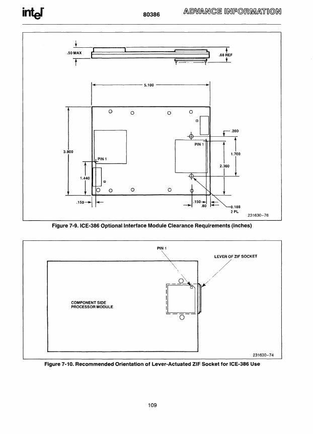
80386
'y
5.100
o o o
.800
o o
i
I f
•
PIN 1
.150-. - .80
+ .68 REF
t
•. 200
! 0.188 2 PL
231630-76
Figure 7-9. ICE-3S6 Optional Interface Module Clearance Requirements (inches)
COMPONENT SIDE PROCESSOR MODULE
PI~
~,
rDl 1: ___ _
o
LEVER OF ZIF SOCKET
231630-74
Figure 7-10. Recommended Orientation of Lever-Actuated ZIF Socket for ICE-3S6 Use
109

intJ 80386
8. INSTRUCTION SET
This section describes the 80386 instruction set. A table lists all instructions along with instruction encoding diagrams and clock counts. Further details of the instruction encoding are then provided in the following sections, which completely describe the encoding structure and the definition of all fields occurring within 80386 instructions.
8.1 80386 INSTRUCTION ENCODING AND CLOCK COUNT SUMMARY
To calculate elapsed time for an instruction, multiply the instruction clock count, as listed in Table 8-1 below, by the processor clock period (e.g. 62.5 ns for an 80386-16 operating at 16 MHz (32 MHz CLK2 signal)). The actual clock count of an 80386 program will average 5% more than the calculated clock count due to instruction sequences which execute faster than they can be fetched from memory.
For more detailed information on the encodings of instructions refer to section 8.2 Instruction Encodings. Section 8.2 explains the general structure of instruction encodings, and defines exactly the encodings of all fields contained within the instruction.
110
Instruction Clock Count Assumptions
1. The instruction has been prefetched, decoded, and is ready for execution.
2. Bus cycles do not require wait states.
3. There are no local bus HOLD requests delaying processor access to the bus.
4. No exceptions are detected during instruction execution.
5. If an effective address is calculated, it does not use two general register components. One register, scaling and displacement can be used within the clock counts shown. However, if the effective address calculation uses two general register components, add 1 clock to the clock count shown.
Instruction Clock Count Notation
1. If two clock counts are given, the smaller refers to a register operand and the larger refers to a memory operand.
2. n = number of times repeated.
3. m = number of components in the next instruction executed, where the entire displacement (if any) counts as one component, the entire immediate data (if any) counts as one component, and all other bytes of the instruction and prefix(es) each count as one component.
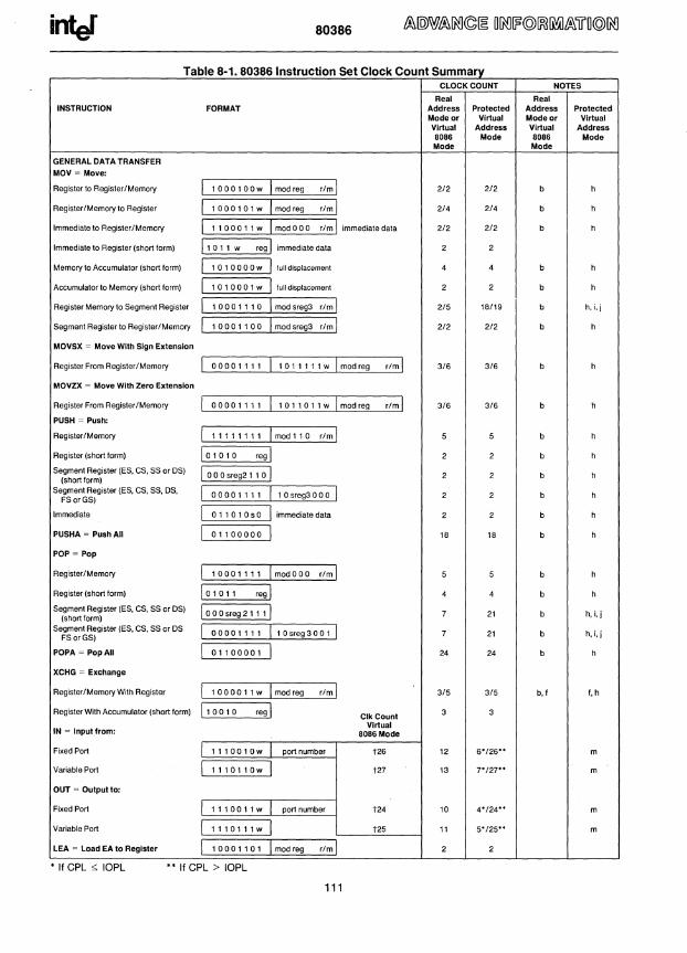
80386
a e T bl 8 -1.8 3 6 o 8 I nstructlon S CI et ock C ount S ummary CLOCK COUNT NOTES
Real Real INSTRUCTION FORMAT Address Protected Address Protected
Mode or Virtual Mode or Virtual Virtual Address Virtual Address 8086 Mode 8086 Mode Mode Mode
GENERAL DATA TRANSFER MOV ~ Move:
Register to Register/Memory I 1000100w I mod reg rim 1 2/2 2/2 b h
Register/Memory to Register I 1000101w I mod reg rim 1 2/4 2/4 b h
Immediate to Register/Memory I 1100011 w 1 modOOO rim 1 immediate data 2/2 2/2 b h
Immediate to Register (short form) 11011 w reg 1 immediate data 2 2
Memory to Accumulator (short form) 1 1010000w 1 full displacement 4 4 b h
Accumulator to Memory (short form) I 1010001w 1 full displacement 2 2 b h
Register Memory to Segment Register I 10001110 I mod sreg3 rIm 1 2/5 18/19 b h, i, j
Segment Register to Register/Memory I 10001100 I mod sreg3 rIm I 2/2 2/2 b h
MOVSX ~ Move With Sign Extension
Register From Register/Memory 1 00001111 1 1011111 w I mod reg rim I 3/6 3/6 b h
MOVZX = Move With Zero Extension
Register From Register/Memory 1 00001111 1 1011011 w I mad reg r/ml 3/6 3/6 b h
PUSH ~ Push:
Register/Memory 11111111 1 mod 110 rim 1 5 5 b h
Register (short form) 01010 reg 1 2 2 b h
Segment Register (ES, es, SS or OS) 000Sreg21101 2 2 b h (short form)
Segment Register (ES, es, SS, OS, 00001 111 1 1 Osreg3000 1 2 2 b h FSorGS)
Immediate 01101050 1 immediate data 2 2 b h
PUSHA ~ Push All 01100000 1 18 18 b h
POP ~ Pop
Register/Memory 1 10001111 1 modOOO rim 1 5 5 b h
Register (short form) 101011 reg I 4 4 b h
Segment Register (ES, es, 55 or OS) 1000Sreg21111 7 21 b h, i,i (shortlorm)
Segment Register (ES, es, 55 or OS I 00001111 1 10sreg3001 1 7 21 b h, i,j FSorGS)
POPA ~ Pop All 1 01100001 1 24 24 b h
XCHG ~ Exchange
Register/Memory With Register 1 1000011w I mod reg rim 1 3/5 3/5 b, f f, h
Register With Accumulator (short form) 110010 reg 1 ClkCount 3 3
IN = Input from: Virtual
8086 Mode
Fixed Port I 1110010w I port number, t26 12 6'/26" m
Variable Port 1 1110110w 1 t27 13 7'/27" m
OUT ~ Output to:
Fixed Port I 1110011 w I port number t24 10 4'/24·· m
Variable Port 1 1110111 w 1 t25 11 5'/25" m
LEA ~ Load EA to Register I 10001101 I mod reg rim 1 2 2
* If CPL <;; IOPL ** If CPL > IOPL
111

intJ 80386
Table 8·1. 80386 Instruction Set Clock Count Summary (Continued) CLOCK COUNT NOTES
Real Real INSTRUCTION FORMAT Address Protected Address Protected - Mode or Virtual Mode or Virtual
Virtual Address Virtual Address 8086 Mode 8086 Mode Mode Mode
SEGMENT CONTROL
LOS ~ Load Pointer to OS 11000101 mod reg rim! 7 22 b h.i.j
LES ~ Load Pointer to ES 11000100 mod reg rim! 7 22 b h.i.j
LFS ~ Load Pointer to FS 00001111 10110100 I mod reg rim! 7 25 b h.i.j
LGS ~ Load Pointer to GS 00001111 10110101 I mod reg rim! 7 25 b h.i.j
LSS ~ Load Pointer to SS 00001111 10110010 I mod reg rim! 7 22 b h. i.j
FLAG CONTROL
CLC ~ Clear Carry Flag I 11111000 2 2
CLD ~ Clear Direction Flag I 11111100 2 2
CLI ~ Clear Interrupt Enable Flag I 11111010 3 3 m
CL TS ~ Clear Task Switched Flag I 00001111 00000110 ! 5 5 c I
CMC ~ Complement Carry Flag I 11110101 2 2
LAHF ~ Load AH Into Flag 10011111 2 2
POPF ~ Pop Flags 10011101 5 5 b h. n
PUSHF ~ Push Flags 10011100 4 4 b h
SAHF ~ Store AH Into Flags 10011110 3 3
STC ~ Set Carry Flag 11111001 2 2
STD ~ Set Direction Flag 11111001 2 2
STI ~ Set Interrupt Enable Flag 11111011 3 3 m
ARITHMETIC ADD ~ Add
Regisler to Register I OOOOOOdw mod reg rim! 2 2
Regisler to Memory I OOOOOOOw mod reg rim! 7 7 b h
Memory to Register I 0000001w mod reg rim! 6 6 b h
Immediale to Register IMemory I 100000sw modOOO rim! immediate data 217 2/7 b h
Immediate to Accumulator (short lorm) I 0000010w immediate data 2 2
ADC ~ Add With Carry
Register to Register I 000100dw mod reg rim! 2 2
Register to Memory I 0001000w mod reg rim! 7 7 b h
Memory to Register I 0001001w mod reg rim! 6 6 b h
Immediate to Register/Memory I 100000sw mod 0 10 rim! immediate data 2/7 217 b h
Immediate to Accumulator (short form) I 0001010w immediate data 2 2
INC ~ Increment
RegisterlMemory I lllllllw ! modOOO rim! 2/6 2/6 b h
Register (short form) 101000 reg ! 2 2
SUB ~ Subtract
Register from Register I OOtOtOdw I mod reg rim! 2 2
112
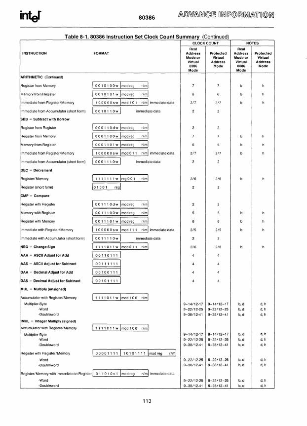
80386
a e -T bl 8 1 80386 I nstructlon et oc S CI kC ount S ummary (C ontlnue d) CLOCK COUNT NOTES
Real Real INSTRUCTION FORMAT Address Protected Address Protected
Mode or Virtual Mode or Virtual Virtual Address Virtual Address 8086 Mode 8086 Mode Mode Mode
ARITHMETIC (Continued)
Register from Memory I 00101 DOw ImOdreg r/ml 7 7 b h
Memory from Register I 0010101w ImOdreg rIm] 6 6 b h
Immediate from Register/Memory I 100000sw ImOdl01 rim] immediate data 217 217 b h
Immediate from Accumulator (short form) I 0010t10wl immediate data 2 2
SSS = Subtract with Borrow
Register from Register I 00011 Odw ImOdreg r/ml 2 2
Register from Memory I 0001 1 00 w I mod reg rIm] 7 7 b h
Memory from Register I 0001 1 01 w I mod feg rIm] 6 6 b h
Immediate from Register/Memory I 1 000 a 0 5 W I mod a 1 1 rIm] immediate data 217 217 b h
Immediate from Accumulator (short form) 10001110wl immediate data 2 2
DEC = Decrement
Register/Memory I 1111111Wlreg001 r/ml 2/6 2/6 b h
Register (short form) 101001 regl 2 2
CMP ~ Compare
Register with Register o 0 1 1 1 0 d w I mod reg r/ml 2 2
Memory with Register 00111 OOw ImOdreg r/ml 5 5 b h
Register with Memory 0011101w ImOdreg r/ml 6 6 b h
Immediate with RegisterlMemory 1 00000 s w I mod 1 1 1 r/ml immediate data 2/5 2/5 b h
Immediate with Accumulator (short form) 001111 Ow I immediate data 2 2
NEG ~ Change Sign I 1 1 1 1 01 1 w I mod 0 1 1 r/ml 2/6 2/6 b h
AAA ~ ASCII Adjust for Add I 00110111 I 4 4
AAS ~ ASCII Adjust for Subtract L 00 111111J 4 4
DAA ~ Decimal Adjust for Add I 00100111 I 4 4
DAS = DeCimal Adjust for Subtract I 00101111 I 4 4
MUL ~ Multiply (unsigned)
Accumulator with RegisterlMemory I 1111011 w ImOd 100 r/ml
Multiplier-Byte 9-14/12-17 9-14/12-17 b, d d, h
-Word 9-22/12-25 9-22/12-25 b, d d, h -Doubleword 9-38/12-41 9-38/12-4f b, d d, h
IMUL = Integer Multiply (signed)
Accumulator with RegisterlMemory I 1111011 w ImOd 1 00 r/ml Multiplier-Byte I 9-14/12-17 9-14/12-17 b,d d, h
-Word
I
9-22/12-25 9-22/12-25 b,d d, h
-Doubleword 9-38/12-41 9-38/12-41 b,d d, h
Register with Register IMemory I 00001111 I 10101111 Imod reg r/ml -Word 9-22/12-25 9-22/12-25 b, d d, h
-Ooubleword 9-38/12-41 9-38/12-41 b,d d, h
RegisterlMemory with Immediate to Register I 01 1010 s 1 Imod reg r/ml immediate data
-Word 9-22/12-25 9-22/12-25 b, d d, h
-Doubleword 9-38/12-41 9-38/12-41 b, d d, h
113

inter 80386
Table 8·1 80386 Instruction Set Clock Count Summary (Continued) CLOCK COUNT NOTES
Real Real INSTRUCTION FORMAT Address Protected Address Protected
Mode or Virtual Mode or Virtual Virtual Address Virtual Address 8086 Mode 8086 Mode Mode Mode
ARITHMETIC (Continued)
DIV ~ Divide (Unsigned)
Accumulator by Register/Memory I 11 11011 w Imod 11 0 r/ml Divisor-Byte 14/17 14/17 b,o e,h
-Word 22/25 22/25 b,e e,h -Doubleword 38/41 38/41 b,e e,h
IDIV ~ Integer Divide (Signed)
Accumulator By Register/Memory I 1111011 w Imod 111 r/ml Divisor-Byte 19/22 19/22 b,e e,h
-Word 27/30 27/30 b,e e,h -Doubleword 43/46 43/46 b,e e,h
AAD ~ ASCII Adjust for Divide I 11010101 I 00001010 I 19 19
AAM ~ ASCII Adjust for Multiply I 11010100 I 00001010 I 17 17
CBW = Convert Byte to Word I 100110001 3 3
CWO ~ Convert Word to Double Word I 10011001 I 2 2
LOGIC
Shift Rotate Instructions
Not Through Carry (ROL, ROR, SAL, SAR, SHL, and SHR)
Register/Memory by 1 11101 OOOw ImOdTTT r/ml 317 317 b h
RegisterlMemory by CL 11101001 w I mod TIT r/ml 3/7 3/7 b h
Register/Memory by Immediate Count I 11 OOOOOw I mod TIT r/mlimmed 8·bit data 3/7 317 b h
Through Carry (RCL and RCR)
Register/Memory by 1 I 1101 OOOw ImOdTIT r/ml 9/10 9/10 b h
RegisterlMemory by CL I 1101001 w I mod TIT r/ml 9/10 9/10 b h
RegisterlMemory by Immediate Count 11 1 00000 w I mod TIT r/ml immed B·bit data 9/10 9/10 b h
TTT Instruction
000 ROL
001 ROR 010 RCL
011 RCR
100 SHL/SAL
101 SHR
111 SAR SHLD ~ Shift Left Double
Register/Memory by Immediate I 00001111 I 1 01 001 00 Imod reg r/mlimmed S-bit data 3/7 3/7
RegisterlMemory by CL I 00001111 I 10100101 ImOdreg r/ml 317 3/7
SHRD ~ Shift Right Double
Register/Memory by Immediate I 00001111 I 10101100 ImOd reg r/ml immed B·bit data 3/7 317
RegisterlMemory by CL I 0000111 1 I 10101101 ImOd reg r/ml 3/7 317
AND ~ And
Register to Register I 001000 d w Imod reg r/ml 2 2
114

80386
Table 8-1. 80386 Instruction Set Clock Count Summary (Continued) CLOCK COUNT NOTES
Real Real INSTRUCTION FORMAT Address Protected Address Protected
Mode or Virtual Mcdeor Virtual Virtual Address Virtual Address 8086 Mode 8086 Mode Mode Mode
LOGIC (Continued)
Register to Memory I OOtOOOOw I mod reg r/ml 7 7 b h
Memory to Register I 0010001w I mod reg r/ml 6 6 b h
Immediate to Register/Memory I 1 OOOOOOw Imodl 00 r/ml immediate data 217 217 b h
Immediate to Accumulator (Short Form) I a 0 1 00 1 Ow I immediate data 2 2
TEST ~ And Function to Flags, No Result
Register/Memory and Register I 1000010w I mod reg r/ml 2/5 2/5 b h
Immediate Data and Register/Memory I tlltOllw ImodOOO r/ml immediate data 2/5 2/5 b h
Immediate Data and Accumulator (Short Form) I 10 1 0 1 DOw I immediate data 2 2
OR ~ Or
Register to Register I 00001 Odw I mod reg r/ml 2 2
Register to Memory I 0000100w I mod reg r/ml 7 7 b h
Memory to Register I 0000 101 w ImOdreg r/ml 6 6 b h
Immediate to Register/Memory I 1 OOOOOOw ImodOOI r/ml immediate data 2/7 217 b h
Immediate to Accumulator (Short Form) I 00 0 0110 w I immediate data 2 2
XOR = Exclusive Or
Register to Register o 0 1 1 0 a d w I mod reg r/ml 2 2
Register to Memory 0011 OOOw ImOdreg r/ml 7 7 b h
Memory to Register 0011001w ImOdreg r/ml 6 6 b h
Immediate to Register/Memory 1 OOOOOOw Imodll 0 r / m I immediate data 2/7 217 b h
Immediate to Accumulator (Short Form) 001101 Ow I immediate data 2 2
NOT ~ Invert Reglster/Memory 1111011 w ImodO 1 0 rim/ Clk
2/6 2/6 b h
STRING MANIPULATION Count Virtual
CMPS ~ Compare Byte Word I 1010011 wi 8086
10 10 b h Mode
INS ~ Input Byte/Word from OX Port I a 11 a 11 Ow I I t29 15 9','29" b h,m
LODS ~ Load Byte/Word to ALI AX/EAX I 10 1 a 11 Ow I 5 5 b h
MOVS ~ Move Byte Word I 1010010wl 7 7 b h
OUTS ~ Output Byte/Word to OX Port I a 11 a 111 wi I t28 14 8'/28" b h,m
SCAS ~ Scan Byte Word I 1010111 wi 7 7 b h
STOS ~ Store Byte/Word from
AL/AX/EX I 1010101 wi 4 4 b h
XLAT ~ Translate String I 11010111 I 5 5 h
REPEATED STRING MANIPULATION
Repeated by Count in ex or ECX
REPE CMPS ~ Compare String
(Find Non-Match) I 11110011 I 1010011 wi 5+9n 5+9n b h
* If CPL ,;; IOPL .* If CPL > IOPL
115

inter 80386
Table 8-1. 80386 Instruction Set Cloc k Count S ummary( c ontlnued)
CLOCK COUNT NOTES
Real Real INSTRUCTION FORMAT Address Protected Address Protected
Modear Virtual Modear Virtual Virtual Address Virtual Address 8086 Mode 8086 Mode Mode Mode
REPEATED STRING MANIPULATION (Continued)
REPNE CMPS ~ Compare String ClkCount
(Find Match) I till 00 1 0 1010011 w Virtual
5+9n 5+9n b h 8086 Mode
REP INS ~ Input String I 11110010 0110110w I t27+6n 13+6n 7 + 6n·'27 + 6n-· b h,m
REP LODS ~ Load String I 11110010 1010110w 5+6n 5+6n b h
REP MOVS ~ Move String I 11110010 1010010w 7+4n 7+4n b h
REP OUTS ~ Output String 111110010 0110111 w I t26+5n 12+5n 6 + 5n-/26 + 5n·· b h,m
REPE SCAS ~ Scan String
(Find Non-ALI AX/EAX) I 1111001111010111Wl 5+8n 5+8n b h
REPNE SCAS ~ Scan String
(Find ALI AX/EAX) I 1111001011010111Wl 5+8n 5+8n b h
REP STOS ~ Store String 11111001011010101Wl 5+5n 5+5n b h
BIT MANIPULATION
BSF ~ Scan Bit Forward I 00001111 I 1 0 1 1 1 1 00 ImOd reg r/ml 10+3n 10+3n b h
BSR ~ Scan Bit Reverse I 00001111 I 1 0 1 1 1 1 00 ImOd reg r/ml 10+3n 10+3n b h
BT ~ Test Bit
Register/Memory. Immediate I 0000 1 1 1 1 I 1 0 1 1 1 0 1 0 Imod 1 00 r/mlirnmed 8-bit data 3/6 3/6 .b h
RegisterlMemory, Register I 00001 111 11 01 0001 1 ImOd reg r/ml 3/12 3/12 b h
BTC ~ Test Bit and Complement
RegisterlMemory, Immediate I 00001111 110111010 Imod 111 r/mj;mmed 8-bit datal 6/8 6/8 b h
RegisterlMemory, Register I 00001111 110111011 ImOd reg r/ml 6/13 6/13 b h
BTR ~ Test Bit and Reset
RegisterlMemory, Immediate I 0000 1 1 1 1 I 1 0 1 1 1 0 1 0 Imod 1 1 0 r/mlimmed a-bit datal 6/8 6/8 b h
Register/Memory, Register I 00001111 11 011 001 1 Imod reg r/ml 6/13 6/13 b h
BTS ~ Test Bit and Set
RegisterlMemory, Immediate I 0000111 1 I 1 01 1 1 01 0 Imod 1 01 r/mlirnmed a-bit datal 6/8 6/8 b h
Register/Memory, Register I 00001111 I 10101011 ImOdreg r/ml 6/13 6/13 b h
BIT STRING MANIPULATION
IBTS ~ Insert Bit String I 00001111 I 10100111 ImOdreg r/ml 12/19 12/19 b h
XBTS ~ Extract Bit String I 00001111 I 1 0 1 00 1 1 0 ImOd reg r/ml 6/13 6/13 b h
CONTROL TRANSFER
CALL ~ Can
Direct Within Segment I 1 1 1 0 1 0 0 0 I full displacement 7+m 7+m b r
Register IMemory
Indirect Within Segment I 11111111 Imodolo r/ml 7+ml 7+ml b h, r 10+m 10+m
Direct Intersegment I 1 00 1 1 0 1 0 lunSigned full offset, selector 17+m 34+m b j,k,r
Notes: t Clock count shown applies if I/O permission allows I/O to the port in virtual 6066 mode_ If I/O bit map denies permission exception 13 fault occurs; refer to clock counts for INT 3 instruction_ • If CPL s; 10PL •• If CPL > 10PL
116

inter 80386
Table 8-1. 80386 Instruction Set Clock Count Summar (Continued) CLOCK COUNT NOTES
Real Real INSTRUCTION FORMAT Address Protected Address Protected
Mode or Virtual Mode or Virtual Virtual Address Virtual Address 8086 Mode 8086 Mode Mode Mode
CONTROL TRANSFER (Continued)
Protected Mode Only (Direct Intersegment)
Via Call Gate to Same Privilege Level 52+m h,j,k,r
Via Call Gate to Different Privilege Level,
(No Parameters) 86+m h,j,k,r
Via Call Gate to Different Privilege Level, (x Parameters) 94+4x+m h,j,k,r
From 286 Task to 286 TSS 235 h,j,k,r
From 286 Task to 386 TSS 265 h,j,k,r
From 286 Task to Virtual 8086 Task (386 TSS) 214 h,j,k,r
From 386 Task to 286 TSS 245 h,j,k,r From 386 Task to 386 TSS 275 h,j,k,r
From 386 Task to Virtual 8086 Task (386 TSS) 224 h,j,k,r
Indirect Intersegment I 11111111 ImodO 11 r/ml 22+m 38+m b h,j,k,r
Protected Mode Only (Indirect Intersegment)
Via Call Gate to Same Privilege Level 56+m h,j,k,r
Via Call Gate to Different Privilege Level, (No Parameters) 90+m h,j,k,r
Via Call Gate to Different Privilege Level. (x Parameters) 98+4x+m h,j,k,r
From 286 Task to 286 TSS 240 h,j,k,r
From 286 Task to 386 TSS 270 h,j,k,r
From 286 Task to Virtual 8086 Task (386 TSS) 218 h,j,k,r
From 386 Task to 286 TSS 250 h,j,k,r
From 386 Task to 386 TSS 280 h,j,k,r From 386 Task to Virtual 8086 Task (386 TSS) 228 h,j,k,r
JMP ~ Uncondillonal Jump
Short I 11101001 la.bit displacement I 7+m 7+m r
Direct within Segment I 11101001 I full displacement 7+m 7+m r
Register/Memory Indirect within Segment I 11111111 I mod 100 r/ml 7+ml 7+ml b h,r 10+m 10+m
Direct Intersegment I 11101010 I unsigned full offset, selector 12+m 27+m j,k,r
Protected Mode Only (Direct Intersegment)
Via Call Gate to Same Privilege Level 45+m h,j,k,r
From 286 Task to 286 TSS 223 h,j,k,r
From 286 Task to 386 TSS 253 h,j,k,r From 286 Task to Virtual 8086 Task (386 TSS) 212 h,j,k,r
From 386 Task to 286 TSS 233 h,j,k,r
From 386 Task to 386 TSS 263 h,j,k,r
From 386 Task to Virtual 8086 Task (386 TSS) 222 h,j,k,r
Indirect Intersegment 111111111 Imod 1 0 1 r/ml 17+m 31+m b h,j,k,r
Protected Mode Only (Indirect Intersegment)
Via Call Gate to Same Privilege Level 49+m h,j,k,r
From 286 Task to 286 TSS 228 h,j,k,r
From 286 Task to 386 TSS 258 h,j,k,r
From 286 Task to Virtual 8086 Task (386 TSS) 216 h,j,k,r
From 386 Task to 286 TSS 238 h,j,k,r
From 386 Task to 386 TSS 268 h,j,k,r
From 386 Task to Virtual 8086 Task (386 TSS) 226 h,j,k,r
117

80386
a e -T bl 8 1 80386 I f ns rue Ion e oe S tCI k C oun tS ummary (C r on Inue d) CLOCK COUNT NOTES
Real Real INSTRUCTION FORMAT Address Protected Address Protected
Mode or Virtual Modecr Virtual Virtual Address Virtual Address 8086 Mode 8086 Mode Mode Mode
CONTROL TRANSFER (Continued)
RET ~ Return from CALL:
Within Segment I 11000011 I 10 + m 10 + m b g, h"
Within Segment Adding Immediate to SP I 11000010 I 16·bit displ I 10 + m 10 + m b g, h"
Intersegment I 11001011 I 18 + m 32+m b g, h,i, k"
Intersegment Adding Immediate to SP I 11001010 I 16·bit displ I 18 + m 32+m b g, h, i, k"
Protected Mode Only (RET):
to Different Privilege Level Intersegment 68 h, i, k" Intersegment Adding Immediate to SP 68 h, i, k"
CONDITIONAL JUMPS
NOTE: Times Are Jump "Taken or Not Taken" JO = Jump on Overflow
a-Bit Displacement I 01110000 I 8·bit displ I 7 + m or3 7 + mor3 , Full Displacement I 00001111 I 10000000 I full displacement 7 + m or 3 7 + mor3 ,
JNO ~ Jump on Not Overflow
8-Bit Displacement I 01110001 I 8·bitdispl I 7 + morS 7 + m or3 , Full Displacement I 00001111 I 10000001 I full displacement 7 + mor3 7 + m or3 ,
JB/JNAE ~ Jump on BelowlNot Above 0' Equal
a-Bit Displacement lO11100101 8·bit displ j 7 + morS 7 + mor3 , Full Displacement l 00001111j 1 00000 1 0 j full displacement 7 + mor3 7 + m or3 ,
JNB/JAE ~ Jumpon Nol Below/Above or Equal
8-Bit Displacement I 01110011 I 8·bit displ I 7 + mor3 7 + mor3 , Full Displacement I 00001111 I 10000011 I full displacement 7 + mor3 7+mor3 ,
JE/JZ ~ Jump on Equal/Zero
8-Bit Displacement I 01110100 I 8·bit displ I 7 + mor3 7 + m or3 , Full Displacement I 00001111 I 10000100 I full displacement 7 + m or3 7 + mor3 ,
JNE/JNZ ~ Jump on Not Equal/Not Zero
8-Bit Displacement I 01110101 I 8·bit displ I 7 + m or3 7+mor3 , Full Displacement I 00001111 I 10000101 I full displacement 7 + mor3 7+mor3 ,
JBE/JNA = Jump on Below or Equal/Not Above
8-Bit Displacement I 01110110 I 8·bitdispl I 7 + mor3 7 + mor3 , Full Displacement I 00001111 I 10000110 I full displacement 7 + mor3 7 + mor3 ,
JNBE/JA ~ Jump on Not Below or Equal/Above
8-Bit Displacement I 01110111 I 8·bit displ I 7 + mor3 7 + m or3 , Full Displacement I 00001111 I 10000111 I full displacement 7 + mor3 7+mor3 ,
JS ~ Jump on Sign
8-Bit Displacement I 01111000 I 8·bitdispl I 7 + mor3 7 + mor3 , Full Displacement I 00001111 I 10001000 I full displacement 7 + mor3 7 + mor3 ,
118
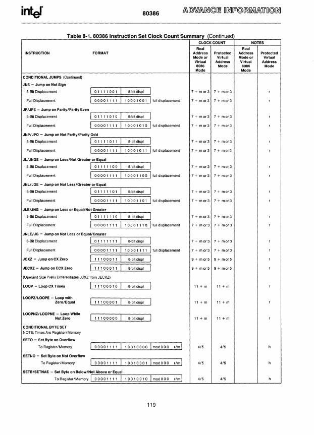
intJ 80386
Table 8-1. 80386 Instruction Set Clock Count Summary (Continued) CLOCK COUNT NOTES
Real Real INSTRUCTION FORMAT Address Protected Address Protected
Mode or Virtual Mode or Virtual Virtual Address Virtual Address 8086 Mode 8086 Mode Mode Mode
CONDITIONAL JUMPS (Continued)
JNS ~ Jump on Not Sign
8~Bit Displacement I 01111001 I 8-bil displ I 7+mor3 7 + mor3 r
Full Displacement I 00001111 I 10001001 I full displacement 7 + mor3 7 + mor3 r
JP/JPE ~ Jump on Parity/Parity Even
8·Bit Displacement I 01111010 I 8-bit displ I 7 + mor3 7 + mor3 r
Full Displacement I 00001111 I 10001010 I full displacement 7 + mor3 7 + mor3 r
JNP/JPO ~ Jump on Not Parity/Parity Odd
8-Bit Displacement I 01111011 I 8-bit displ I 7 + mor3 7 + mor3 r
Full Displacement I 00001111 I 10001011 I full displacement 7+mor3 7 + mor3 r
JL/JNGE ~ Jump on LesslNot Greater or Equal
8-Bit Displacement I 01111100 I 8-bit displ I 7 + mor3 7 + mor3 r
Full Displacement I 00001111 I 10001100 I full displacement 7 + mor3 7 + mor3 r
JNLlJGE ~ Jump on Not Less/Greater or Equal
8-Bit Displacement I 01111101 I 8-bitdispl I 7 + mor3 7 + mor3 r
Full Displacement I 00001111 I 10001101 I full displacement 7 + mor3 7 + mor3 r
JLE/JNG ~ Jump on Less or Equal/Not Greater
a-Bit Displacement I 01111110 I 8-bitdispl I 7 + mor3 7 + mor3 r
Full Displacement I 00001111 I 10001110 I full displacement 7+mor3 7 + mor3 r
JNLE/JG ~ Jump on Not Less or Equal/Greater
a-Bit Displacement I 01111111 I 8-bitdispl I 7 + morS 7 + morS r
Full Displacement I 00001111 I 10001111 I full displacement 7 + m or3 7 + mor3 r
JCXZ ~ Jump on CX Zero I 11100011 I 8-bitdispl I 9 + marS 9 + morS r
JECXZ ~ Jump on ECX Zero I 11100011 I 8-bitdispl I 9 + morS 9 + mor5 r
(Operand Size Prefix Differentiates JCXZ from JECXZ)
LOOP ~ Loop CX Times I 11100010 I 8-bitdispl I 11 + m 11 + m r
LOOPZ/LOOPE ~ Loop with Zero/Equal I 11100001 I 8-bitdispl I 11 + m 11 + m r
LOOPNZ/LOOPNE ~ Loop While Not Zero I 11100000 I 8-bitdispl I 11 +m 11 + m r
CONDITIONAL BYTE SET NOTE: Times Are Register/Memory
SETO ~ Set Byte on Overflow
To Register/Memory I 00001111 I 10010000 I modOOO r/ml 4/5 4/5 h
SETNO ~ Set Byte on Not Overflow
To Register/Memory I 00001111 I 10010001 I modOOO rim I 4/5 4/5 h
SETBISETNAE ~ Set Byte on Below/Not Above or Equal
To Register/Memory I 00001111 I 10010010 I modOOO r/mi 4/5 4/5 h
119
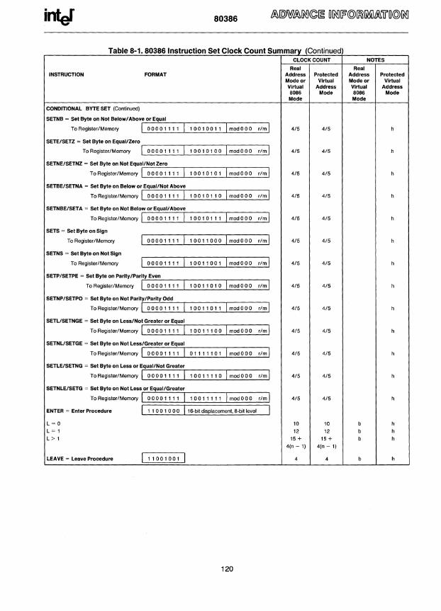
80386
Table 8-1. 80386 Instruction Set Clock Count Summary (Continued) CLOCK COUNT NOTES
Real Real INSTRUCTION FORMAT Address Protected Address Protected
Mode or Virtual Mode or Virtual Virtual Address Virtual Address 8086 Mode 8086 Mode Mode Mode
CONDITIONAL BYTE SET (Continued)
SETNB ~ Set Byte on Not Below/Above or Equal
To Register/Memory I 00001111 I 10010011 I modOOO rIm I 4/5 4/5 h
SETE/SETZ ~ Set Byte on EquallZero
To Register/Memory I 00001111 I 10010100 I modOOO rim I 4/5 4/5 h
SETNE/SETNZ ~ Set Byte on Not EquallNot Zero
To Register/Memory I 00001111 I 10010101 I modOOO r/m' 4/5 4/5 h
SETBE/SETNA ~ Set Byte on Below or EquallNot Above
To Register/Memory I 0000 1 1 1 1 I 10010110 I modOOO r/m' 4/5 4/5 h
SETNBE/SETA ~ Set Byte on Not Below or Equall Above
To Register/Memory I 00001111 I 10010111 I modOOO r/m' 4/5 4/5 h
SETS ~ Set Byte on Sign
To Register/Memory I 00001111 I 10011000 I modOOO r/m' 4/5 4/5 h
SETNS ~ Set Byte on Not Sign
To Register/Memory I 00001111 I 10011001 I modOOO r/m' 4/5 4/5 h
SETP/SETPE ~ Set Byte on Parlty/Parlty Even
To Register/Memory I 00001111 I 10011010 , modOOO r/m' 4/5 4/5 h
SETNP/SETPO ~ Set Byte on Not Parlty/Parlty Odd
To Register/Memory I 000011 11 I 10011011 I modOOO rIm' 4/5 4/5 h
SETUSETNGE ~ Set Byte on LesslNot Greater or Equal
To Register/Memory I 0000 1 1 1 1 I 10011100 I modOOO rIm' 4/5 4/5 h
SETNL/SETGE ~ Set Byte on Not Less/Greater or Equal
To Register/Memory I 0000 1 1 1 1 ,
01111101 I modOOO rIm' 4/5 4/5 h
SETLE/SETNG ~ Set Byte on Less or EquallNot Greater
To Register/Memory I 00001111 I 10011110 I modOOO rim' 4/5 4/5 h
SETNLE/SETG ~ Set Byte on Not Less or EquallGreater
To Register/Memory I 0000 1 1 1 1 I 10011111 I modOOO rim I 4/5 4/5 h
ENTER ~ Enter Procedure I 1 1 0 0 1 0 0 0 liS-bit displacement, S-bit level I L~O 10 10 b h L~ 1 12 12 b h L> 1 15 + 15 + b h
4(n - 1) 4(n - 1)
LEAVE ~ Leave Procedure I 11001001 ,
4 4 b h
120
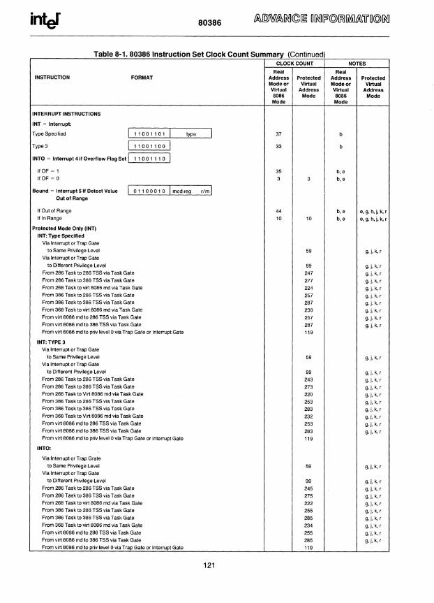
80386
a e -T bl 8 1 80386 I nstructlon et oc S CI kC oun tS ummaay (C ontmue d) CLOCK COUNT NOTES
Real Real INSTRUCTION FORMAT Address Protected Address Protected
Mode or Virtual Mode or Virtual Virtual Address Virtual Address 8086 Mode 8086 Mode Mode Mode
INTERRUPT INSTRUCTIONS
INT ~ Interrupt:
Type Specified I 11001101 I type I 37 b
Type 3 I 11001100 I 33 b
INTO ~ Interrupt 4 II Overflow Flag Set I 11001110 I If OF ~ 1 35 b,e If OF ~ 0 3 3 b, e
Bound = Interrupt Sit Oetect Value I 01100010 I mod reg r/ml Outot Range
If Out of Range 44 b, e e, g, h,j, k, r If In Range 10 10 b, e e, g, h,j, k, r
Protected Mode Only (lNT)
INT: Type Specilled
Via Interrupt or Trap Gate
to Same Privilege Level 59 g,j, k, r Via Interrupt or Trap Gate
to Different Privilege Level 99 g, j, k, r From 286 Task to 286 TSS via Task Gate 247 g, j, k, r From 286 Task to 386 TSS via Task Gate 277 g, j, k, r From 268 Task to virt 8086 md via Task Gate 224 g, j, k, r From 386 Task to 286 TSS via Task Gate 257 g, j, k, r From 386 Task to 386 TSS via Task Gate 287 g, j, k, r From 368 Task to virt B086 md via Task Gate 238 g, j, k, r From virt 8086 md to 286 TSS via Task Gate 257 g, j, k, r From virt 8086 md to 386 TSS via Task Gate 287 g, j, k, r From virt 8086 md to priv level 0 via Trap Gate or Interrupt Gate 119
INT:TVPE 3
Via Interrupt or Trap Gate
to Same Privilege Level 59 g, j, k, r Via Interrupt or Trap Gate
to Different Privilege Level 99 g,j, k, r From 286 Task to 286 TSS via Task Gate 243 g, j, k, r From 286 Task to 386 TSS via Task Gate 273 g, j, k, r From 268 Task to Virt 8086 md via Task Gate 220 g, j, k, r From 386 Task to 286 TSS via Task Gate 253 g, j, k, r From 386 Task to 386 TSS via Task Gate 283 g, j, k, r From 368 Task to Virt 8086 md via Task Gate 232 g, j, k, r From virt 8086 md to 286 TSS via Task Gate 253 g, j, k, r From virt 8086 md to 386 TSS via Task Gate 283 g, j, k, r From virt 8086 md to priv level 0 via Trap Gate or Interrupt Gate 119
INTO:
Via Interrupt or Trap Grate
to Same Privilege Level 59 g, j, k, r Via Interrupt or Trap Gate
to Different Privilege Level 99 g, j, k, r From 286 Task to 286 TSS via Task Gate 245 g, j, k, r From 286 Task to 386 TSS via Task Gate 275 g,j, k, r From 268 Task to virt 8086 md via Task Gate 222 g,j, k, r From 386 Task to 286 TSS via Task Gate 255 g,j, k, r From 386 Task to 386 TSS via Task Gate 285 g,j, k, r From 368 Task to virt 8086 md via Task Gate 234 g,j, k, r From virt 8086 md to 286 TSS via Task Gate 255 g, j, k, r From virt 8086 md to 386 TSS via Task Gate 285 g, j, k, r From virt 8086 md to priv level 0 via Trap Gate or Interrupt Gate 119
121
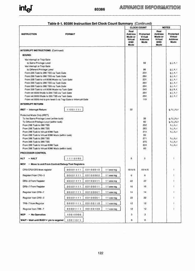
intJ 80386
T bl a e 8-1. 8 o 61 38 nstructlon et oc S CI kC ount S ummary (C ontlnue d) CLOCK COUNT NOTES
Real Real INSTRUCTION FORMAT Address Protected Address Protected
Mode or Virtual Mode or Virtual Virtual Address Virtual Addresa 8086 Mode 8086 Mode Mode Mode
INTERRUPT INSTRUCTIONS (Continued)
BOUND:
Via Interrupt or Trap Gate to Same Privilege Level 59 g,i, k, r
Via Interrupt or Trap Gate
to Different Privilege Level 99 g,i, k, r
From 286 Task to 286 TSS via Task Gate 254 g,i,k,r
From 286 Task to 386 TSS via Task Gate 284 g,i,k,r
From 268 Task to virt 8086 Mode via Task Gate 231 g,i,k,r
From 386 Task to 286 TSS via Task Gate 264 g,i, k, r
From 386 Task to 386 TSS via Task Gate 294 g,i, k, r
From 368 Task to virt 8086 Mode via Task Gate 243 g,i, k, r,
From virt 8086 Mode to 286 TSS via Task Gate 264 g,i, k, r
From virt 8086 Mode to 386 TSS via Task Gate 294 g,i, k, r
From virt 8086 md to priv level 0 via Trap Gate or Interrupt Gate 119
INTERRUPT RETURN
IRET = Interrupt Return I 11001111 I 22 g, h,i,k,r
Protected Mode Only (IRET)
To the Same Privilege Level (within task) 38 g, h,i,k,r
To DiHerent Privilege Level (within task) 82 g, h,i,k,r
From 286 Task to 286 TSS 232 h,i, k, r
From 286 Task to 386 TSS 265 h,i, k, r
From 286 Task to Virtual 8086 Task 214 h,i, k, r
From 286 Task to Virtual 8086 Mode (within task) 60
From 386 Task to 286 TSS 271 h,i, k, r
From 386 Task to 386 TSS 275 h,i, k, r
From 386 Task to Virtual 8086 Task 224 h,i, k, r
From 386 Task to Virtual 8086 Mode (within task) 60
PROCESSOR CONTROL
HLT = HALT I 11110100 I 5 5 I
MOV = Move to and From Control/DebuglTest Registers
CRO/CR2/CR3 from register I 00001111 00100010 11 eee reg 10/4/5 10/4/5 I
Register From CRO-3 I 00001111 00100000 11 eee reg 6 6 I
DRO-3 From Register I 00001111 00100011 11 eee reg 22 22 I
DR6-7 From Register I 00001111 00100011 11 eee reg 16 16 I
Register from DR6-7 I 00001111 00100001 11 eeereg 14 14 I
Register from DRO-3 I 00001111 00100001 11 eeereg 22 22 I
TR6-7 from Register I 00001111 00100110 11 eeereg 12 12 I
Register from TR6-7 I 00001111 00100100 11 eee reg 12 12 I
NOP = No Operation I 10010000 3 3
WAIT = Wail until BUSY# pin Is negated I 10011011 6 6
122
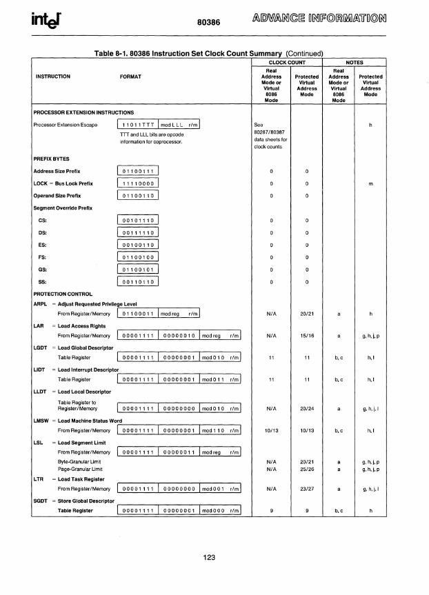
infef 80386
a e T bl 8 -1. 803 86 nstructlon et oc S CI kC ount S ummary (C ontlnue d) CLOCK COUNT NOTES
Real Real INSTRUCTION FORMAT Address Protected Address Protected
Mode or Virtual Mode or Virtual Virtual Address Virtual Address 8086 Mode 8086 Mode Mode Mode
PROCESSOR EXTENSION INSTRUCTIONS
Processor Extension Escape 111011 TTT I modLLL rim I See h
Tn and LLL bits are opcode 80287/80387
information for coprocessor. data sheets for clock counts
PREFIX BYTES
Address Size Prellx I 01100111 I 0 0
LOCK ~ Bus Lock Prellx I 11110000 I 0 0 m
Operand Size Prellx I 01100110 I 0 0
Segment Override Prellx
CS: 00101110 0 0
DS: 00111110 0 0
ES: 00100110 0 0
FS: 01100100 0 0
GS: 01100101 0 0
ss: 00110110 0 0
PROTECTION CONTROL
ARPL ~ Adjust Requested Privilege Level
From Register/Memory I 01100011 I mod reg rim I N/A 20/21 a h
LAR ~ Load Access Rights
From RegislerlMemory I 00001111 I 00000010 I mod reg rim I N/A 15/16 a g, h,j,p
LGDT ~ Load Global Descriptor
Table Register I 00001111 I 00000001 ImodOl0 rim I 11 11 b,c h, I
LIDT ~ Load Interrupt Descriptor
Table Register I 00001111 I 00000001 I modOll rim I 11 11 b, c h, I
LLDT ~ Load Local Descriptor
Table Register 10 RegisterlMemory I 00001111 I 00000000 I modOl0 rim I N/A 20/24 a g, h,j,1
LMSW ~ Load Machine Status Word
From RegisterlMemory I 00001111 I 00000001 I modll 0 rim I 10/13 10/13 b,c h, I
LSL ~ Load Segment Limit
From RegisterlMemory I 00001111 I 00000011 I mod reg rim I
Byte-Granular Limit N/A 20/21 a g, h,j, P Page-Granular Limit N/A 25/26 a g,h,j,p
LTR ~ Load Task Register
From RegislerlMemory I 00001111 I 00000000 I modOOl r/ml N/A 23/27 a g, h,j,1
SGDT ~ Store Global Descriptor
Table Register I 00001111 I 00000001 I modOOO rim I 9 9 b, c h
123

infef 80386
a e -1. T bl 8 803861 ns rue Ion e oe t" StCI kC ount 5 ummary (C ontlnue d) CLOCK COUNT NOTES
Real Real INSTRUCTION FORMAT Address Protected Address Protected
Madear Virtual Modear Virtual Virtual Address Virtual Address 8086 Mode 8086 Mode Mode Mode
SlOT ~ Store Interrupt Descriptor
Table Register I 00001111 I 00000001 ImodOOl rIm I 9 9 b,c h
SLOT ~ Store Local Descriptor Table Register
To Register/Memory I 00001111 I 00000000 I modOOO rIm! N/A 2/2 a h
SMSW ~ Store Machine Status Word I 00001111 I 00000001 Imodl00 rIm! 10/13 10/13 b,c h, I
STR ~ Store Task Register
To RegisterlMemory I 00001111 I 00000000 ! modOO 1 rIm! N/A 2/2 a h
VERR ~ Verify Read Accesss
Register/Memory I 00001111 I 00000000 I modI 00 r/ml N/A 10/11 a g, h,j, P
VERW ~ Verify Write Accesss I 00001111 I 00000000 I modI 01 r/ml N/A 15/16 a g, h,j, P
INSTRUCTION NOTES FOR TABLE 8-1
Notes a through c apply to 80386 Real Address Mode only: a. This is a Protected Mode instruction. Attempted execution in Real Mode will result in exception 6 (invalid opcode). b. Exception 13 fault (general protection) will occur in Real Mode if an operand reference is made that partially or fully extends beyond the maximum CS, OS, ES, FS or GS limit, FFFFH. Exception 12 fault (stack segment limit violation or not present) will occur in Real Mode if an operand reference is made that partially or fully extends beyond the maximum SS limit. c. This instruction may be executed in Real Mode. In Real Mode, its purpose is primarily to initialize the CPU for Protected Mode.
Notes d throughg apply to 80386 Real Address Mode and 80386 Protected Virtual Address Mode: d. The iAPX 386 uses an early-out multiply algorithm. The actual number of clocks depends on the pOSition of the most significant bit in the operand (multiplier).
Clock counts given are minimum to maximum. To calculate actual clocks use the following formula: Actual Clock = if m < > 0 then max ([IOg2 Imll. 3) + 6 clocks:
if m = 0 then 9 clocks (where m is the multiplier) e. An exception may occur, depending on the value of the operand. f. LOCK# is automatically asserted, regardless of the presence or absence of the LOCK# prefix. g. LOCK # is asserted during descriptor table accesses.
Notes h through r apply to 80386 Protected Virtual Address Mode only: h. Exception 13 fault (general protection violation) will occur if the memory operand in CS, OS, ES, FS or GS cannot be used due to either a segment limit violation or access rights violation. If a stack limit is violated, an exception 12 (stack segment limit violation or not present) occurs. i. For segment load operations, the CPL, RPL, and OPL must agree with the privilege rules to avoid an exception 13 fault (general protection violation). The segment's descriptor must indicate "present" or exception 11 (CS, OS, ES, FS, GS not present). If the SS register is loaded and a stack segment not present is detected, an exception 12 (stack segment limit violation or not present) occurs. j. All segment descriptor accesses in the GOT or LOT made by this instruction will automatically assert LOCK# to maintain descriptor integrity in multiprocessor systems. k. JMP, CALL, INT, RET and IRET instructions referring to another code segment will cause an exception 13 (general protection violation) if an applicable privilege rule is violated. I. An exception 13 fault occurs if CPL is greater than 0 (0 is the most privileged level). m. An exception 13 fault occurs if CPL is greater than IOPL. n. The IF bit of the flag register is not updated if CPL is greater than IOPL. The IOPL and VM fields of the flag register are updated only if CPL = O. o. The PE bit of the MSW (CRO) cannot be reset by this instruction. Use MOV into CRO if desiring to reset the PE bit. p. Any violation of privilege rules as applied to the selector operand does not cause a protection exception; rather, the zero flag is cleared. q. If the coprocessor's memory operand violates a segment limit or segment access rights, an exception 13 fault (general protection exception) will occur before the ESC instruction is executed. An exception 12 fault (stack segment limit violation or not present) will occur if the stack limit is violated by the operand's starting address. r. The destination of a JMP, CALL, INT, RET or IRET must be in the defined limit of a code segment or an exception 13 fault (general protection violation) will occur.
124
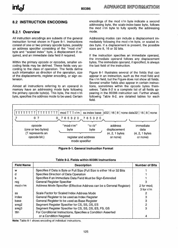
inter 80386
8.2 INSTRUCTION ENCODING
8.2.1 Overview
All instruction encodings are subsets of the general instruction format shown in Figure 8-1. Instructions consist of one or two primary opcode bytes, possibly an address specifier consisting of the "mod rim" byte and "scaled index" byte, a displacement if required, and an immediate data field if required.
Within the primary opcode or opcodes, smaller encoding fields may be defined. These fields vary according to the class of operation. The fields define such information as direction of the operation, size of the displacements, register encoding, or sign extension.
Almost all instructions referring to an operand in memory have an addressing mode byte following the primary opcode byte(s). This byte, the mod rim byte, specifies the address mode to be used. Certain
encodings of the mod rim byte indicate a second addressing byte, the scale-index-base byte, follows the mod rim byte to fully specify the addressing mode.
Addressing modes can include a displacement immediately following the mod rim byte, or scaled index byte. If a displacement is present, the possible sizes are 8, 16 or 32 bits.
If the instruction specifies an immediate operand, the immediate operand follows any displacement bytes. The immediate operand, if specified, is always the last field of the instruction.
Figure 8-1 illustrates several of the fields that can appear in an instruction, such as the mod field and the rim field, but the Figure does not show all fields. Several smaller fields also appear in certain instructions, sometimes within the opcode bytes themselves. Table 8-2 is a complete list of all fields appearing in the 80386 instruction set. Further ahead, following Table 8-2, are detailed tables for each field.
ITTTTTTT T I TTT TTTTT I mod TTT rim I ss index base Id32i16i8i none data32i16i8i none
:z 07 o)~~~\ )
opcode (one or two bytes) (T represents an
opcode bit.)
"mod rim" "s-i-b" byte byte
\~--------~--------~)
register and address mode specifier
address displacement (4, 2, 1 bytes
or none)
Figure 8-1. General Instruction Format
Table 8-2. Fields within 80386 Instructions
Field Name Description
w Specifies if Data is Byte or Full Size (Full Size is either 16 or 32 Bits d Specifies Direction of Data Operation s Specifies if an Immediate Data Field Must be Sign-Extended reg General Register Specifier mod rim Address Mode Specifier (Effective Address can be a General Register)
ss Scale Factor for Scaled Index Address Mode index General Register to be used as Index Register base General Register to be used as Base Register sreg2 Segment Register Specifier for CS, SS, OS, ES sreg3 Segment Register Specifier for CS, SS, OS, ES, FS, GS tttn For Conditional Instructions, Specifies a Condition Asserted
or a Condition Negated
Note: Table 8-1 shows encoding of individual instructions.
125
immediate data
(4, 2, 1 bytes or none)
Number of Bits
1 1 1 3
2 for mod; 3 for rim
2 3 3 2 3
4
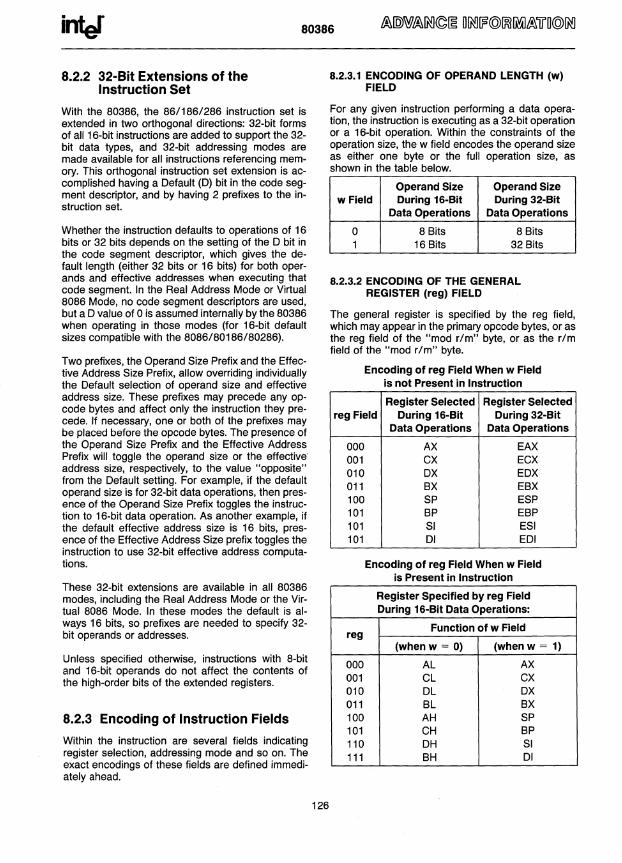
80386
8.2.2 32-Bit Extensions of the Instruction Set
With the 80386, the 86/186/286 instruction set is extended in two orthogonal directions: 32-bit forms of all 16-bit instructions are added to support the 32-bit data types, and 32-bit addressing modes are made available for all instructions referencing memory. This orthogonal instruction set extension is accomplished having a Default (D) bit in the code segment descriptor, and by having 2 prefixes to the instruction set.
Whether the instruction defaults to operations of 16 bits or 32 bits depends on the setting of the 0 bit in the code segment descriptor, which gives the default length (either 32 bits or 16 bits) for both operands and effective addresses when executing that code segment. In the Real Address Mode or Virtual 8086 Mode, no code segment descriptors are used, but a 0 value of 0 is assumed internally by the 80386 when operating in those modes (for 16-bit default sizes compatible with the 8086/80186/80286).
Two prefixes, the Operand Size Prefix and the Effective Address Size Prefix, allow overriding individually the Default selection of operand size and effective address size. These prefixes may precede any opcode bytes and affect only the instruction they precede. If necessary, one or both of the prefixes may be placed before the opcode bytes. The presence of the Operand Size Prefix and the Effective Address Prefix will toggle the operand size or the effective address size, respectively, to the value "opposite" from the Default setting. For example, if the default operand size is for 32-bit data operations, then presence of the Operand Size Prefix toggles the instruction to 16-bit data operation. As another example, if the default effective address size is 16 bits, presence of the Effective Address Size prefix toggles the instruction to use 32-bit effective address computations.
These 32-bit extensions are available in all 80386 modes, including the Real Address Mode or the Virtual 8086 Mode. In these modes the default is always 16 bits, so prefixes are needed to specify 32-bit operands or addresses.
Unless specified otherwise, instructions with 8-bit and 16-bit operands do not affect the contents of the high-order bits of the extended registers.
8.2.3 Encoding of Instruction Fields
Within the instruction are several fields indicating register selection, addreSSing mode and so on. The exact encodings of these fields are defined immediately ahead.
126
8.2.3.1 ENCODING OF OPERAND LENGTH (w) FIELD
For any given instruction performing a data operation, the instruction is executing as a 32-bit operation or a 16-bit operation. Within the constraints of the operation size, the w field encodes the operand size as either one byte or the full operation size, as shown in the table below.
Operand Size Operand Size wField During 16·8it During 32·8it
Data Operations Data Operations
0 8 Bits 8 Bits 1 16 Bits 32 Bits
8.2.3.2 ENCODING OF THE GENERAL REGISTER (reg) FIELD
The general register is specified by the reg field, which may appear in the primary opcode bytes, or as the reg field of the "mod rim" byte, or as the rim field of the "mod rim" byte.
Encoding of reg Field When w Field is not Present in Instruction
Register Selected Register Selected reg Field During 16·8it During 32·8it
000 001 010 011 100 101 101 101
reg
000 001 010 011 100 101 110 111
Data Operations Data Operations
AX EAX CX ECX OX EDX BX EBX SP ESP BP EBP SI ESI 01 EDI
Encoding of reg Field When w Field is Present in Instruction
Register Specified by reg Field During 16·8it Data Operations:
Function of w Field
(when w = 0) (when w = 1)
AL AX CL CX DL OX BL BX AH SP CH BP DH SI BH 01

80386
Register Specified by reg Field During 32-Bit Data Operations
Function of w Field reg
(whenw = 0) (whenw = 1)
000 AL EAX 001 CL ECX 010 DL EDX 011 BL EBX 100 AH ESP 101 CH EBP 110 DH ESI 111 BH EDI
8.2.3.3 ENCODING OF THE SEGMENT REGISTER (sreg) FIELD
The sreg field in certain instructions is a 2-bit field allowing one of the four 80286 segment registers to be specified. The sreg field in other instructions is a 3-bit field, allowing the 80386 FS and GS segment registers to be specified.
2-Bit sreg2 Field
2-Bit Segment
sreg2 Field Register Selected
00 ES 01 CS 10 SS 11 DS
3-Bit sreg3 Field
3-Bit Segment
sreg3 Field Register Selected
000 ES 001 CS 010 SS 011 DS 100 FS 101 GS 110 do not use 111 do not use
127
8.2.3.4 ENCODING OF ADDRESS MODE
Except for special instructions, such as PUSH or POP, where the addressing mode is pre-determined, the addressing mode for the current instruction is specified by addressing bytes following the primary opcode. The primary addressing byte is the "mod rim" byte, and a second byte of addressing information, the "s-i-b" (scale-index-base) byte, can be specified.
The s-i-b byte (scale-index-base byte) is specified when using 32-bit addressing mode and the "mod rim" byte has rim = 100 and mod = 00,01 or 10. When the sib byte is present, the 32-bit addressing mode is a function of the mod, ss, index, and base fields.
The primary addressing byte, the "mod rim" byte, also contains three bits (shown as TTT in Figure 8-1) sometimes used as an extension of the primary opcode. The three bits, however, may also be used as a register field (reg).
When calculating an effective address, either 16-bit addressing or 32-bit addressing is used. 16-bit ad· dressing uses 16-bit address components to calculate the effective address while 32-bit addressing uses 32-bit address components to calculate the effective address. When 16-bit addressing is used, the "mod rim" byte is interpreted as a 16-bit addressing mode specifier. When 32-bit addressing is used, the "mod rim" byte is interpreted as a 32·bit addressing mode specifier.
Tables on the following three pages define all encodings of all 16-bit addressing modes and 32-bit addressing modes.
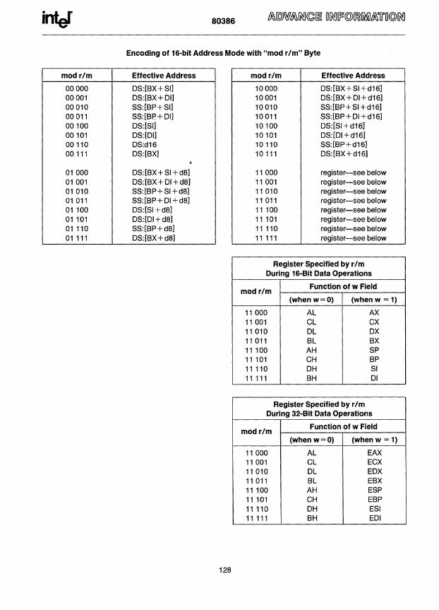
infef 80386
Encoding of 16·bit Address Mode with "mod rIm" Byte
mod rIm Effective Address mod rIm Effective Address
00000 OS:[BX+Sil 10000 OS:[BX+SI +d16) 00001 OS:[BX+Oil 10001 OS:[BX + 01 + d16) 00010 SS:[BP+Sil 10010 SS:[BP+SI+d16) 00011 SS:[BP+Oil 10011 SS:[BP+ 01 + d16) 00100 OS:[Sil 10100 OS: [SI + d16) 00101 OS:[Oil 10101 OS: [01 + d16) 00110 OS:d16 10110 SS: [BP + d16) 00111 OS:[BX) 10 111 OS:[BX+d16)
,. 01000 OS: [BX + SI + dB) 11000 register-see below 01 001 OS: [BX + 01 + dB) 11 001 register-see below 01 010 SS:[BP+SI+dB) 11 010 register-see below 01011 SS: [BP + 01 + dB) 11 011 register-see below 01100 OS:[SI+dB) 11 100 register-see below 01 101 OS:[OI + dB) 11 101 register-see below 01 110 SS:[BP+dB) 11 110 register-see below 01 111 OS:[BX+dB) 11 111 register-see below
Register Specified by rIm During 16·Bit Data Operations
mod rIm Function of w Field
(when w=O) (when w = 1)
11000 AL AX 11 001 CL CX 11 010 OL OX 11 011 BL BX 11 100 AH SP 11 101 CH BP 11 110 OH SI 11 111 BH 01
Register Specified by rIm During 32·Bit Data Operations
mod rIm Function of w Field
(when w=O) (when w = 1)
11000 AL EAX 11 001 CL ECX 11010 OL EOX 11 011 BL EBX 11 100 AH ESP 11 101 CH EBP 11 110 OH ESI 11 111 BH EOI
12B
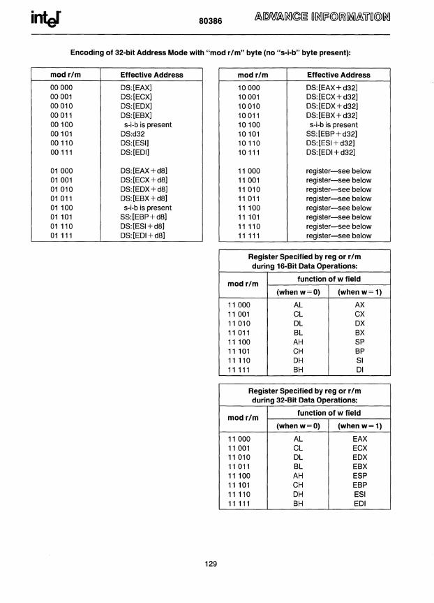
inter 80386
Encoding of 32-bit Address Mode with "mod rIm" byte (no "s-i-b" byte present):
mod rIm Effective Address mod rIm Effective Address
00000 OS: [EAX) 10000 OS:[EAX+d32) 00001 OS: [ECX) 10001 OS: [ECX + d32) 00010 OS:[EOX) 10010 OS: [EOX + d32) 00011 OS:[EBX) 10011 OS: [EBX + d32) 00100 s-i-b is present 10100 s-i-b is present 00101 OS:d32 10101 SS: [EBP + d32) 00110 OS: [ESI) 10110 OS: [ESI + d32) 00111 OS:[EOI) 10 111 OS: [EOI + d32)
01000 OS:[EAX+dS) 11 000 register-see below 01001 OS: [ECX + dS) 11001 register-see below 01 010 OS:[EOX+dS) 11010 register-see below 01 011 OS:[EBX+dS) 11 011 register-see below 01 100 s-i-b is present 11 100 register-see below 01 101 SS: [EBP + dS) 11 101 register-see below 01 110 OS: [ESI + dS) 11 110 register-see below 01 111 OS: [EOI + dS) 11 111 register-see below
Register Specified by reg or rIm during 16-Bit Data Operations:
mod rIm function of w field
(when w=O) (when w= 1)
11000 AL AX 11001 CL CX 11 010 DL DX 11 011 BL BX 11100 AH SP 11 101 CH BP 11 110 DH SI 11 111 BH 01
Register Specified by reg or rIm during 32-Bit Data Operations:
mod rIm function of w field
(whenw=O) (whenw= 1)
11 000 AL EAX 11001 CL ECX 11 010 OL EOX 11 011 BL EBX 11100 AH ESP 11 101 CH EBP 11 110 DH ESI 11 111 BH EDI
129

intJ 80386
Encoding of 32-bit Address Mode ("mod rim" byte and "s-i-b" byte present):
mod base Effective Address
00000 OS: [EAX + (scaled index)] 00001 OS: [ECX + (scaled index)] 00010 OS: [EOX + (scaled index)] 00011 OS: [ESX + (scaled index)] 00100 SS: [ESP + (scaled index)] 00101 OS: [d32 + (scaled index)] 00110 OS:[ESI + (scaled index)] 00111 OS: [EOI + (scaled index)]
01000 OS: [EAX + (scaled index) + dB] 01001 OS: [ECX + (scaled index) + dB] 01010 OS: [EOX + (scaled index) + dB] 01011 OS: [ESX + (scaled index) + dB] 01100 SS; [ESP + (scaled index) + dB] 01101 SS: [ESP + (scaled index) + dB] 01110 OS: [ESI + (scaled index) + dB] 01 111 OS: [EO I + (scaled index) + dB]
10000 OS: [EAX + (scaled index) + d32] 10001 OS: [ECX + (scaled index) + d32] 10010 OS: [EOX + (scaled index) + d32] 10011 OS: [ESX + (scaled index) + d32] 10100 SS; [ESP + (scaled index) + d32] 10101 SS: [ESP + (scaled index) + d32] 10110 OS: [ESI + (scaled index) + d32] 10 111 OS: [EOI + (scaled index) + d32]
NOTE: Mod field in "mod rim" byte; ss, index, base fields in "s-i-b" byte.
130
ss Scale Factor
00 x1 01 x2 10 x4 11 xB
index Index Register
000 EAX 001 ECX 010 EOX 011 ESX 100 no index reg* * 101 ESP 110 ESI 111 EOI
"IMPORTANT NOTE: When index field is 100, indicating "no index register," then ss field MUST equal 00. If index is 100 and ss does not equal 00, the effective address is undefined.

80386
8.2.3.5 ENCODING OF OPERATION DIRECTION (d) FIELD
In many two·operand instructions the d field is pres· ent to indicate which operand is considered the source and which is the destination.
d Direction of Operation
0 Register/Memory <- - Register "reg" Field Indicates Source Operand; "mod r/m" or "mod ss index base" Indicates Destination Operand
1 Register <- - Register/Memory "reg" Field Indicates Destination Operand; "mod r/m" or "mod ss index base" Indicates Source Operand
8.2.3.6 ENCODING OF SIGN-EXTEND (s) FIELD
The s field occurs primarily to instructions with immediate data fields. The s field has an effect only if the size of the immediate data is 8 bits and is being placed in a 1S-bit or 32-bit destination.
Effect on Effect on s Immediate Data8 Immediate Data 16132
None None
1 Sign-Extend Data8 to Fill None 1S-Bit or 32-Bit Destination
8.2.3.7 ENCODING OF CONDITIONAL TEST (tttn) FIELD
For the conditional instructions (conditional jumps and set on condition), tttn is encoded with n indicating to use the condition (n = 0) or its negation (n = 1), and ttt giving the condition to test.
131
Mnemonic Condition tttn
0 Overflow 0000 NO No Overflow 0001 B/NAE Below/Not Above or Equal 0010 NB/AE Not Below/Above or Equal 0011 E/Z Equal/Zero 0100 NE/NZ Not EquallNot Zero 0101 BEINA Below or EquallNot Above 0110 NBE/A Not Below or Equal/ Above 0111 S Sign 1000 NS Not Sign 1001 PIPE Parity/Parity Even 1010 NP/PO Not Parity/Parity Odd 1011 L/NGE Less Than/Not Greater or Equal 1100 NL/GE Not Less Than/Greater or Equal 1101 LEING Less Than or Equal/Greater Than 1110 NLE/G Not Less or Equal/Greater Than 1111
8.2.3.8 ENCODING OF CONTROL OR DEBUG OR TEST REGISTER (eee) FIELD
For the loading and storing of the Control, Debug and Test registers.
When Interpreted as Control Register Field
eeeCode Reg Name
000 CRO 010 CR2 011 CR3
Do not use any other encoding
When Interpreted as Debug Register Field
eeeCode Reg Name
000 DRO 001 DR1 010 DR2 011 DR3 110 DRS 111 DR7
Do not use any other encoding
When Interpreted as Test Register Field
eeeCode Reg Name
110 TRS 111 TR7
Do not use any other encoding

ALABAMA
Intel Corp 5015 Bradford Drive SUite 2 Huntsville 35805 Tel (205) 830-4010
ARIZONA
Intel Corp 11225 N 28th Drive SUile 2140 PhoeniX 85029 Tel (602) 869-4980
Intel Corp 1161 N. EI Dorado Place SUlle 301 Tucson 85715 Tel. (602) 299-6815
CALIFORNIA
Intel Corp 21515 Vanowen Street SUite 116 Canoga Park 91303 Tel' (818) 704·8500
Inlel Corp 2250 E Impeflal Highway SUite 218 EI Segundo 90245 Tel' (213) 640·6040
Intel Corp. 1510 Arden Way. SUite 101 Sacramento 95815 Tel: (916) 920·8096
Intel Corp. 4350 Executive Drive SUite 105 San Diego 92121 (619) 452·5880
Intel Corp' 2000 East 4th Street SUite 100 Santa Ana 92705 Tel' (714) 835-9642 TWX 910·595-1114
Intel Corp' San Thomas 4 2700 San Thomas Expressway Santa Clara, CA 95051 Tel: (408) 986-8086 910·338·0255
COLORADO
Intel Corp 3300 Mitchell lane. SUite 210 Boulder 80301 Tel. (303) 442-8088
Intel Corp 4445 Nor1hpark Drive SUite 100 Colorado Springs 80907 Tel (303) 594·6622
Intel Corp' 650 S Cherry Street SUite 915 Denver 80222 Tel. (303) 321-8086 TWX: 910-931·2289
CONNECTICUT
Intel Corp 26 Mill Plain Road Danbury 06810 Tel: (203) 748-3130 TWX 710-456·1199
EMC Corp. 222 Summer Streel Stamlord 06901 Tel: (203) 327-2934
FLORIDA
Intel Corp 242 N. Westmonte Olive SUite 105 Altamonte Springs 32714 Tel: (305) 869-5588
Inlel Corp. 6363 NW. 6th Way, SUite 100 FI. Lauderdale 33309 Tel: (305) 771-0600 TWX: 510-956·9407
DOMESTIC SALES OFFICES
FLORIDA (Conl'd)
Intel Corp 11300 4th Sireet North Surte 170 St Petersburg 33702 Tet (813) 577·2413
GEORGIA
Intel Corp 3280 POinte Parkway SUite 200 Norcross 30092 Tel (404) 449-054t
ILLINOIS
Intel Corp' 300 N. Mar1ln9ale Road, SUtte 400 Schaumburg 60172 Tel' (312) 310-8031
INDIANA
Intel Corp. 8777 Purdue Road SUite 125 Indianapolis 46268 Tel' (317) 875-0623
IOWA
Intel Corp St Andrews Building 1930 SI. Andrews Olive N E Cedar Rapids 52402 Tel (319) 393·5510
KANSAS
Intel Corp 8400 W. 110th Street SUite 170 Overland Park 66210 Tel (913) 345·2727
MARYLAND
Intel Corp.' 7321 Parkway DrIVe South SUite C Hanover 21076 Tel' (301) 796-7500 TWX: 710-862·1944
Intel Corp 7833 Walker Dilve Greenbelt 20710 Tel' (301) 441-1020
MASSACHUSETTS
Inlel Corp' Westford Corp Center 3 Carlisle Road Westlord 01886 Tel' (617) 692·3222 TWX' 710-343-6333
MICHIGAN
Irltel Corp. 7071 Orchard Lake Road Suite 100 West Bloomfield 48033 Tel (313) 851-8096
MINNESOTA
Inlel Corp 3500 W 80th Street Suite 360 Bloomington 55431 Tel (612) 835-6722 TWX. 910-576-2867
MISSOURI
Intel Corp 4203 Earth City Expressway SUite 131 Earth City 63045 Tel: (314) 291-1990
NEW JERSEY
Intel Corp.' Parkway 109 Office Center 328 Newman Sprmgs Road Red Bank 07101 Tel (201) 747-2233
Intel Corp 75 Llvin9ston Avenue First Floor Roseland 07068 Tel: (201) 740-0111
NEW MEXICO
Intel Corp 8500 Menual Boulevard N.E SUite B 295 Albuquerque 87112 Tel' (505) 292·8086
NEW YORK
Inlel Corp.' 300 Vanderbilt Motor Parkway Hauppauge 11788 Tel' (516) 231·3300 TWX' 510·227·6236
Intel Corp SUite 28 Hollowbrook Park 15 Myers Corners Road Wappmger Falls 12590 Tel: (914) 297-6161 TWX- 510-248·0060
Intel Corp' 211 White Spruce Boulevard Rochester 14623 Tel: (716) 424·1050 TWX 510·253·7391
NORTH CAROLINA
Intel Corp 5700 Executive Center Drive SUite 213 Charlolle 28212 Tel: (704) 568-8966
Intel Corp 2700 Wycliff Road SUite 102 Raleigh 27607 Tel. (919) 781·8022
OHIO
Intel Corp' 6500 Poe Avenue Dayton 45414 Tel. (513) 890-5350 TWX 810·450·2528
Intel Corp.' Chagrin-Brainard Bldg, No 300 28001 Chagnn Boulevard Cleveland 44122 Tel. (216) 464·2736 TWX 810-427·9298
OKLAHOMA
Intel Corp 6801 N Broadway SUite 115 Oklahoma City 73116 Tel: (405) 848-8086
OREGON
Inlel Corp 10700 SW Beaverton Hillsdale Highway SUite 22 Beaverton 97005 Tel (503) 641-8086 TWX 910·467·8741
PENNSYLVANIA
Intel Corp 1513 Cedar Cliff Dnve Camphlll 17011 Tel (717) 737·5035
Intel Corp' 455 Pennsylvama Avenue Fort Washmglon 19034 Tel. (215) 641·1000 TWX. 510·661-2077
Intel Corp' 400 Penn Center Boulevard Suite 610 Pittsburgh 15235 Tel (412) 823-4970
PUERTO RICO
Intel Microprocessor Corp South Industrial Park Las Piedras 00671 Tel' (809) 733·3030
TEXAS
Intel Corp 313 E Anderson Lane SUite 314 Austm 78752 Tel: (512) 454-3628
TEXAS (Cont'd)
Intel Corp' 12300 Ford Road SUite 380 Dallas 75234 Tel. (214) 241-8087 TWX' 910·860-5617
Inlel Corp' 7322 SW. Freeway Suite 1490 Houston 77074 Tel' (713) 988-8086 TWX' 910·881·2490
Industrial Digital Systems Corp 5925 Sovereign Suite 101 Houston 71036 Tel (713)988-9421
UTAH
Intel Corp. 5201 Green Street SUite 290 Murray 84123 Tel (801) 263·8051
VIRGINIA
Intel Corp 1603 Santa Rosa Road SUite 109 Richmond 23288 Tel. (804) 282·5668
WASHINGTON
Intel Corp 110 IlOth Avenue N E SUite 510 Bellevue 98004 Tel: (206) 453·8086 TWX 910-443-3002
Intel Corp 408 N. Mullan Road SUite 102 Spokane 99206 Tel: (509) 928-8086
WISCONSIN
Intel Corp 450 N Sunnyslope Road SUite 130 Chancellory Park I Brooklleld 53005 Tel (414) 784·8087
CANADA BRITISH COLUMBIA
Intel Semiconductor 01 Canada, Ltd 301-2245 W. Broadway Vancouver V6K 2E4 Tel: (604) 738-6522
ONTARIO
Intel Semiconductor of Canada, Ltd 2650 Queerlsvlew Orrve SUite 250 Onawa K2B 8HB Tel: (613) 829-9714 TELEX' 053-4115
Intel Semiconductor of Canada. Ltd 190 Attwell Dflve SUite 500 Rexdale M9W 6Ha Tel. (416) 675-2105 TELEX' 06983574
aUEBEC
Intel Semiconductor of Canada, Ltd 620 S1. Jean Blvd Pointe Claire H9R 3K3 Tel: (514) 694·9130 TWX: 514-694·9134
'Field Application Location
UNITED STATES Intel Corporation 3065 Bowers Avenue Santa Clara, CA 95051
JAPAN Intel Japan K.K. 5,6 Tokodai Toyosato,machi Tsukuba,gun, Ibaraki,ken 300,26 Japan
FRANCE Intel Paris 1 Rue Edison, BP 303 78054 Saint,Quentin en Yvelines France
UNITED KINGDOM Intel Corporation (U.K.) Ltd. Piper's Way Swindon Wiltshire, England SN~ 1RJ
WEST GERMANY Intel Semiconductor GmbH Seidlstrasse 27 D,8000 Munchen 2 West Germany
Order Number: 231746·001
Printed in U.S.A. /HE·311 /0486/20K/BL JM © Intel Corporation 1986