FACSIMILE SERVICE MANUAL - Index of
74
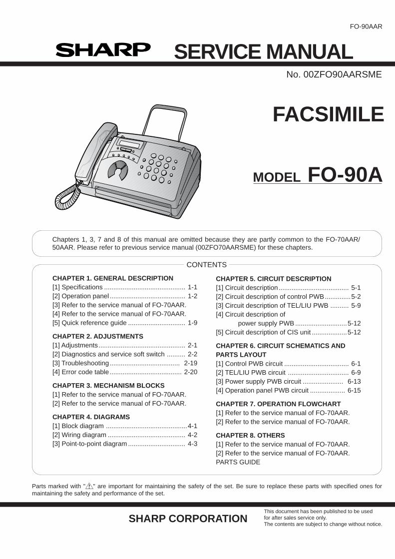
FO-90AAR No. 00ZFO90AARSME CHAPTER 1. GENERAL DESCRIPTION [1] Specifications ............................................ 1-1 [2] Operation panel ......................................... 1-2 [3] Refer to the service manual of FO-70AAR. [4] Refer to the service manual of FO-70AAR. [5] Quick reference guide ............................... 1-9 CHAPTER 2. ADJUSTMENTS [1] Adjustments ............................................... 2-1 [2] Diagnostics and service soft switch .......... 2-2 [3] Troubleshooting ...................................... 2-19 [4] Error code table ....................................... 2-20 CHAPTER 3. MECHANISM BLOCKS [1] Refer to the service manual of FO-70AAR. [2] Refer to the service manual of FO-70AAR. CHAPTER 4. DIAGRAMS [1] Block diagram ............................................ 4-1 [2] Wiring diagram .......................................... 4-2 [3] Point-to-point diagram ............................... 4-3 CHAPTER 5. CIRCUIT DESCRIPTION [1] Circuit description ...................................... 5-1 [2] Circuit description of control PWB .............. 5-2 [3] Circuit description of TEL/LIU PWB .......... 5-9 [4] Circuit description of power supply PWB ............................ 5-12 [5] Circuit description of CIS unit ................... 5-12 CHAPTER 6. CIRCUIT SCHEMATICS AND PARTS LAYOUT [1] Control PWB circuit ................................... 6-1 [2] TEL/LIU PWB circuit ................................. 6-9 [3] Power supply PWB circuit ...................... 6-13 [4] Operation panel PWB circuit ................... 6-15 CHAPTER 7. OPERATION FLOWCHART [1] Refer to the service manual of FO-70AAR. [2] Refer to the service manual of FO-70AAR. CHAPTER 8. OTHERS [1] Refer to the service manual of FO-70AAR. [2] Refer to the service manual of FO-70AAR. PARTS GUIDE CONTENTS FACSIMILE MODEL FO-90A Parts marked with " " are important for maintaining the safety of the set. Be sure to replace these parts with specified ones for maintaining the safety and performance of the set. This document has been published to be used for after sales service only. The contents are subject to change without notice. SHARP CORPORATION SERVICE MANUAL Chapters 1, 3, 7 and 8 of this manual are omitted because they are partly common to the FO-70AAR/ 50AAR. Please refer to previous service manual (00ZFO70AARSME) for these chapters.
-
Upload
khangminh22 -
Category
Documents
-
view
0 -
download
0
Transcript of FACSIMILE SERVICE MANUAL - Index of
FO-90AAR
No. 00ZFO90AARSME
CHAPTER 1. GENERAL DESCRIPTION[1] Specifications ............................................ 1-1[2] Operation panel ......................................... 1-2[3] Refer to the service manual of FO-70AAR.[4] Refer to the service manual of FO-70AAR.[5] Quick reference guide ............................... 1-9
CHAPTER 2. ADJUSTMENTS[1] Adjustments............................................... 2-1[2] Diagnostics and service soft switch .......... 2-2[3] Troubleshooting...................................... 2-19[4] Error code table ....................................... 2-20
CHAPTER 3. MECHANISM BLOCKS[1] Refer to the service manual of FO-70AAR.[2] Refer to the service manual of FO-70AAR.
CHAPTER 4. DIAGRAMS[1] Block diagram ............................................4-1[2] Wiring diagram .......................................... 4-2[3] Point-to-point diagram ............................... 4-3
CHAPTER 5. CIRCUIT DESCRIPTION[1] Circuit description...................................... 5-1[2] Circuit description of control PWB..............5-2[3] Circuit description of TEL/LIU PWB .......... 5-9[4] Circuit description of power supply PWB ............................5-12[5] Circuit description of CIS unit ...................5-12
CHAPTER 6. CIRCUIT SCHEMATICS ANDPARTS LAYOUT[1] Control PWB circuit ................................... 6-1[2] TEL/LIU PWB circuit ................................. 6-9[3] Power supply PWB circuit ...................... 6-13[4] Operation panel PWB circuit ................... 6-15
CHAPTER 7. OPERATION FLOWCHART[1] Refer to the service manual of FO-70AAR.[2] Refer to the service manual of FO-70AAR.
CHAPTER 8. OTHERS[1] Refer to the service manual of FO-70AAR.[2] Refer to the service manual of FO-70AAR.PARTS GUIDE
CONTENTS
FACSIMILE
MODEL FO-90A
Parts marked with " " are important for maintaining the safety of the set. Be sure to replace these parts with specified ones formaintaining the safety and performance of the set.
This document has been published to be usedfor after sales service only.The contents are subject to change without notice.
SHARP CORPORATION
SERVICE MANUAL
Chapters 1, 3, 7 and 8 of this manual are omitted because they are partly common to the FO-70AAR/50AAR. Please refer to previous service manual (00ZFO70AARSME) for these chapters.

FO-90AAR
(Danish) ADVARSEL !Lithiumbatteri-Eksplosionsfare ved fejlagtig håndtering.
Udskiftning må kun ske med batteri af samme fabrikat og type.Levér det brugte batteri tilbage til leverandoren.
(English) Caution !Danger of explosion if battery is incorrectly replaced.
Replace only with the same or equivalent typerecommended by the equipment manufacturer.
Discard used batteries according to manufacturer’sinstructions.
(Finnish) VAROITUSParisto voi räjähtää, jos se on virheellisesti asennettu.
Vaihda paristo ainoastaan laitevalmistajan suosittelemaantyyppiin. Hävitä käytetty paristo valmistajan ohjeiden
mukaisesti.
(French) ATTENTIONIl y a danger d’explosion s’ il y a remplacement incorrect
de la batterie. Remplacer uniquement avec une batterie dumême type ou d’un type recommandé par le constructeur.Mettre au rébut les batteries usagées conformément aux
instructions du fabricant.
(Swedish) VARNINGExplosionsfare vid felaktigt batteribyte.
Använd samma batterityp eller en ekvivalenttyp som rekommenderas av apparattillverkaren.
Kassera använt batteri enligt fabrikantensinstruktion.
(German) AchtungExplosionsgefahr bei Verwendung inkorrekter Batterien.
Als Ersatzbatterien dürfen nur Batterien vom gleichen Typ odervom Hersteller empfohlene Batterien verwendet werden.Entsorgung der gebrauchten Batterien nur nach den vom
Hersteller angegebenen Anweisungen.
CAUTION FOR BATTERY REPLACEMENT

FO-90AAR
CHAPTER 1. GENERAL DESCRIPTION
[1] SpecificationsAutomatic dialing: Rapid Key Dialing: 5 numbers
Speed Dialing: 35 numbers
Fax paper: Initial starter roll (included with machine): 10 mRecommended replacement roll: FO-20PRw, 30m
Paper cutting method: Automatic cutter
Modem speed: 9600 bps with automatic fallback to lowerspeeds
Transmission time* : Approx. 15 seconds
Resolution: Horizontal: 8 dots/mmVertical:
Standard: 3.85 lines/mmFine/Halftone: 7.7 lines/mmSuper fine: 15.4 lines/mm
Automatic document feeder: 5 pages max. (20 lb paper)
Halftone (grayscale): 64 levels
Display: 16-digit LCD display
Compression scheme: MR, MH, Sharp (H2)
Applicable telephone line: Public switched telephone network
Compatibility: ITU-T (CCITT) G3 mode
Input document size: Automatic feeding:Width: 148 to 216 mmLength: 140 to 297 mm
Manual feeding:Width: 148 to 216 mmLength: 140 to 600 mm
Effective scanning width: 210 mm max.
Effective printing width: 210 mm max.
Contrast control: Automatic/Dark selectable
Reception modes: Fax, Tel, Tel/Fax, T.C.D
Copy function: Yes
Telephone function: Yes (cannot be used if power fails)
Power requirements: 220-240 V AC, 50/60 Hz
Operating temperature: 5 - 35°C
Humidity: Maximum: 85 % RH
Power consumption: Standby: 2.6 WMaximum: 115 W
Dimensions: Width: 304 mmDepth: 236 mmHeight: 122 mm
Weight: Approx. 2.6 kg
* Based on ITU-T (CCITT) Test Chart #1 at standard resolution in Sharpspecial mode, excluding time for protocol signals (i.e., ITU-T phase Ctime only).
Note: The facsimile machine is Year 2000 compliant.
As a part of our policy of continuous improvement, SHARP reserves the right to make design and specification changes for procductimprovement without prior notice. The performance specifications figures indicated are nominal values of production units. There may be somedeviation from these values in individual units.
1 – 1

FO-90AAR
1 – 2
[2] Operation panel
12
1 4 5 62 3 7
151413 16 17 18
1. Teclas de discado rápido (Rapid Dial keys) Press one of these keys to dial a fax or voice number automatically.2. Tecla GRABACION/MEMORIA (REC/MEMO key) Press this key to record a phone conversation or a message.3. Tecla RETROCESO (REPEAT key) Press this key to repeat playback of a message.4. Tecla FUNCIONAR/OMITIR (PLAY/SKIP key) Press this key to play recorded messages. During playback, press it to skip forward to the next message.5. Pantalla de cristal líquido (Display) This displays messages and prompts during operation and programming.6. Tecla BORRAR (DELETE key) Press this key to erase recorded messages.7. Tecla FUNCIÓN (FUNCTION key) Press this key to select various special functions.8. Tecla VOLUMEN (VOLUME keys) Press this keys to adjust the volume of the speaker when the SPEAKER key has been pressed, the volume of the handset when the handset is lifted, or the volume of the ringer at all other times.9. Teclas numéricas (Number keys) Use these keys to dial numbers, and enter numbers and letters when storing auto-dial numbers.
10. Tecla DISCADO RÁPIDO (SPEED DIAL key) Press this key to dial a fax or voice number using an abbreviated 2-digit Speed Dial number.11. Tecla REDISCADO (REDIAL key) Press this key to automatically redial the last number dialed.12. Tecla EMPEZAR/MEMORIA (START/MEMORY key) Press this key to send or receive a document, or to scan a document into memory before sending it.13. Tecla PARE (STOP key) Press this key to cancel operation before it is completed.14. Tecla COPIA/AYUDA (COPY/HELP key) When a document is in the feeder, press this key to make a copy of a document. At any other time, press this key to print out the Help List, a quick reference guide to the opeation of your fax machine.15. Tecla RESOLUCIÓN/MODO DE RECEPCIÓN (RESOLUTION/RECEPTION MODE key) When a document is in the feeder, press this key to adjust the resolution for faxing or copying. At any other time, press this key to select the reception mode (an arrow in the display will point to the currently selected reception mode).16. Tecla PARLANTE (SPEAKER key) Press this key to listen the line and fax tones through the speaker when faxing a document. Note: This is not a speakerphone. You must pick up the handset to talk with the other party.17. Tecla RETENCIÓN/BÚSQUEDA (HOLD/SEARCH key) Press this key to search for an auto-dial number, or, during a phone conversation, press this key to put the other party on hold.18. Liberación del panel (Panel release) Grasp this finger hold and pull toward you to open the operation panel.
TEL FAX
WXYZ
GHI
PQRS
JKL
ABC DEF
MNO
WXYZTUV
E SONDEO
1 2 3
654
7 8 9
0
TEL FAX
A
GRABACION/MEMORIA RETROCESO FUNCIONAR/
OMITIR BORRAR
B C D
TCD
PARE
COPIA/AYUDAEMPEZAR/
MEMORIA
FUNCION
VOLUMEN
DISCADORAPIDO
REDISCADO
RETENCION/BUSQUEDA
PARLANTERESOLUCION/
MODO DE RECEPCIONFUNC. LENTO FUNC. RAPIDO
8 9 10 11
TEL/FAX

FO-90AAR
TEL/FAX mode: The fax machine automatically answers on the set number ofrings and receives faxes. Voice calls (including manually dialed fax transmissions)are signalled by a special ringing sound.
A.M. mode: Select this mode when you go out to receive both voice messagesand faxes.
SETTING THE DISPLAY LANGUAGE
1. Press:
2. Press:
3. Press the # key or key until the desired language appears in the display.
4. Press:
5. Press:
RECORDING AN OUTGOING MESSAGE
1. Press:
Display shows: OGM RECORDING
2. Press:
3. Press 1 (GENERAL) to record an outgoing message for the answering ma-chine. Press 2 (TRANSFER) to record an outgoing message for the Transferfunction.
4. Pick up the handset, press the START/MEMORY key, and speak into the hand-set ro record your message.
5. When finished, press the STOP key or replace the handset.
6. Press:
[5] Quick reference guideENTERING YOUR NAME AND NUMBER
1. Press: FUNCION
3
Display shows: FIJAR # PROPIO
2. Press:
3. Enter your fax number (max. of 20 digits) by pressing the number keys.
• To insert a space between digits, press the # key.
• If you make a mistake, press the SPEED DIAL key to backspace and clear themistake.
4. Press:
5. Enter your name by pressing the appropriate number keys as shown below.• To enter two letters in succession that require the same key, press the SPEAKER
key after entering the first letter.
Normal Dialing1. Lift the handset or press
2. Dial the fax number.
3. Wait for the reception tone (if a person answers, ask them to press their Startkey).
4. Press:
Rapid Key DialingPress the appropriate Rapid Key. Transmission will begin automatically.
Speed Dialing
1. Press:
2. Enter 2-digit Speed Dial number.
3. Press:
RECEIVING FAXES
Press the RESOLUTION/RECEPTION MODE key until the arrow in the displaypoints to the desired reception mode (make sure the document feeder is empty).
RESOLUCION/MODO DE RECEPCION
FAXTEL
FAXTEL
05 NOV 10:30T.C.DTEL/FAX
T.C.DTEL/FAX
05 NOV 10:30
FAXTEL
FAXTEL
05 NOV 10:30T.C.DTEL/FAX
T.C.DTEL/FAX
05 NOV 10:30
EMPEZAR/MEMORIA
PARLANTE
DISCADORAPIDO
A =
B =
C =
D =
E =
F =
G =
H =
I =
J =
K =
L =
M =
N =
O =
P =
Q =
R =
S =
T =
U =
V =
W =
X =
Y =
Z =
SPACE =
Beep EMPEZAR/MEMORIA
RECIBIENDO
EMPEZAR/MEMORIA
EMPEZAR/MEMORIA
EMPEZAR/MEMORIA
FUNCION
0
FUNCION
4
EMPEZAR/MEMORIA
EMPEZAR/MEMORIA
PARE
PAREPARE
EMPEZAR/MEMORIA
SETTING THE DATE AND TIME
1. Press:
Display shows: FIJAR DIA/FECHA
2. Press:
3. Enter two digits for the Day (01 through 31).
4. Enter two digits for the Month (01 through 12).
5. Enter four digits for the Year (Ex: 2000).
6. Enter two digits for the Hour (01 through 23) and two digits for the Minute (00through 59).
7. When finished, press:
STORING AND CLEARING AUTO DIAL NUMBERS
1. Press:
Display shows: MODO # FAX/TEL
2. Press 1 to store a number or 2 to clear a number.
3. Enter a 2-digit Speed Dial number (from 01 to 05 for Rapid Key Dialing, or 06to 40 for Speed Dialing) (If you are clearing a number, go to Step 7.)
4. Enter the full fax/telephone number.
5. Press:
6. Enter the name of the location by pressing number keys (Refer to the letterentry table in ENTERING YOUR NAME AND NUMBER.)
7. Press:
SENDING FAXES
• To change case, press the REDIAL key.Press # or to scroll through symbols and special characters.
6. When finished, press: EMPEZAR/MEMORIA
PARE
FUNCION
3
FUNCION
3
EMPEZAR/MEMORIA
EMPEZAR/MEMORIA
PARE
EMPEZAR/MEMORIA
EMPEZAR/MEMORIA
PARE
Place your document (up to 5 pages)face down in the document feeder.
FAX mode: The fax machine automatically answers on four rings and receives theincoming document.
TEL mode:
1 – 9

FO-90AAR
M E M O
1 – 10

FO-90AAR
CHAPTER 2. ADJUSTMENTS
[1] Adjustments
GeneralSince the following adjustments and settings are provided for this model,make adjustments and/or setup as necessary.
1. Adjustments
Adjustments of output voltage (FACTORY ONLY)1. Install the power supply unit in the machine.
2. Set the recording paper and document.
3. When the document is loaded, power is supplied to the output lines.Confirm that outputs are within the limits below.
Output voltage settings
3. Settings
Dial mode selectorDIAL mode (Soft Switch No. SWB4 DATA No. 2)
1 DG2 +5V3 MG
4 MG5 +24V6 +24V7 DG8 PSAVE
2 – 1
TEL/LIU PWB POWER SUPPLY PWB
CNL IUACN2
CNPW
CONTROL PWB
CN
L IU
B
CNLIUBCNLIUA
(step 1) Select "FIJAR OPCIONES".
KEY : FUNCION 4
DISPLAY: FIJAR OPCIONES OPRIMA O #
(step 2) Select "MODO DISCADO".
KEY: Push # until " MODO DISCADO " is indicated because the number of # s changes by the model.
DISPLAY: MODO DISCADO
(step 3) Select, using "1" or "2".
KEY: 1
DISPLAY: TONO SELECC
KEY: 2
DISPLAY: PULSO SELECC
(step 4) End, using the "PARE" key.
KEY:
CursorWhen initially registering,the mode shows 1=TONE.When registering again, themode which was registeredformerly is shown.
PARE
1=TONO, 2=PULSO
Output Voltage limits+5V 4.75V ∼ 5.25V+24V 24.0V ∼ 26.0V
ConnectorNo. CNPW
Pin No.
2. IC protectors replacementICPs (IC Protectors) are installed to protect the motor driver circuit.ICPs protect various ICs and electronic circuits from an overcurrent con-dition.
The location of ICPs are shown below:
CNLIUA CNPW
CONTROL PWB(TOP SIDE)
CNMT
FU100
CNLIUB
(1) FU100 (KAB2402) is installed in order to protect IC’s from an over-current generated in the motor drive circuit. If FU100 is open, re-place it with a new one.
4. Volume settingYou can adjust the volume of the speaker, ringer, and handset using theVOLUME key.
(1) Speaker
1 Press the SPEAKER key.
2 Press the VOLUME key one or more times to select the desired level.
The display will show:
VOLUMEN:[ ]
3 Press the SPEAKER key once again to turn off the speaker.
(2) Ringer1 Press the VOLUME key to select the desired volume. (Make sure the
SPEAKER key has not been pressed and the handset is not lifted.)
The display will show:
2 If you want to turn off the ringer, continue to press the VOLUME keyuntil RINGER OFF: OK? appears in the display, and then press theSTART key.
VOLUMEN TIMBRE

FO-90AAR
2. Diagnostic items
ITEM DIRECT
No. keyContents Function
1 — SOFT SWITCH MODE Soft switches are displayed and changed. List can be output.
2 A ROM & RAM CHECK ROM is sum-checked, and RAM is matched. Result list is output.
3 — AGING MODE 10 sheets of check patterns are output every 5 minutes per sheet.
4 — PANEL CKECK MODE Panel keys are tested. Result list is output.
5 B CHECK PATTERN 2 sheets of check patterns are output.
6 C SIGNAL SEND MODE Various signals of FAX communication are output.
7 — MEMORY CLEAR Back-up memory is cleared, and is set at delivery.
8 — SHADING MODE Shading compensation is performed in this mode.
9 D ALL BLACK PRINT To check the print head, whole dots are printed over the interval of 2 m.
10 E AUTO FEEDER MODE Insertion and discharge of document are tested.
11 — ENTRY DATA SEND Registered content is sent.
12 — ENTRY DATA RECEIVE Registered content is received, and its list is output.
13 — MESSAGE PRINT The display message of each language is printed out together with the English equivalent.
14 — FLASH MEMORY CHECK Checks flash memory write/read.
15 — FLASH MEMORY CLEAR Checks flash memory clearing.
16 — CUTTER AGING Recording paper is successively cut.
17 — COUNTRY SELECT The software parameter that it agreed in each country name is set up.
[2] Diagnostics and service soft switch
1. Operating procedure
(1) Entering the diagnostic mode
Press FUNC → 9 → → 8 → # → 7 , and the following display will appear.
ROM Ver. FNY0 After 2 sec: DIAG MODE
FNY0
Then press the START key and country name selected by country select will appear. Select the desired item with the key or the # key or selectwith the direct key. Enter the mode with the START key.
(Diag•specifications)
If the diag mode cannot be set, repeat the diag modeoperation, per-forming the following operation.After the power is turned on and "WAIT A MOMENT"is indicated, press the STOP key.
In relation with the process response (request from ProductionEngineering) "WAIT A MOMENT" clock indication may appear dependingon STOP key timing. If the STOP key is held down, "MEMORY CLEAR?"appears.
FUNC DIAG MODE9 8 7
START —Soft switch mode
START AROM & RAM check
START —Aging mode
START —Panel check mode
START BCheck pattern
START CSignal send mode
START
STARTKEYSTOP
KEY
+"Power ON"
Memory clear(Work + Backup)
FNY0
START —Memory clear
START —Shading mode Entry data send
START
START
Entry data receive
START— Message print
START—
Flash memory check
Flash memory clear
START—
Auto feeder modeSTARTE
—
—
START Cutter aging—
START DAll black mode
START Country selct—
2 – 2

FO-90AAR
3. Diagnostic items description3. 1. Soft switch mode
The soft switches are provided so that each operation mode can be setby using the operation panel.
In this mode, these switches can be checked and set.
The contents of these switches are backed up.
The available soft switches are SW-A1 to SW-K1.
The content of soft switches is shown in page 2-5 to 2-18.
The contents are set to factory default settings.
3. 2. ROM & RAM checkROM executes the sum check, and RAM executes the matching test.The result will be notified with the number of short sounds of the buzzeras well as by printing the ROM & RAM check list.Number of short sounds of buzzer 0 → No error
1 → ROM error
2 → RAM error (32Kbyte)
3. 3. Aging modeIf any document is first present, copying will be executed sheet by sheet.If no document is present, the check pattern will be printed sheet bysheet. This operation will be executed at a rate of one sheet per 5min-utes, and will be ended at a total of 10 sheets.
3. 4. Panel check modeThis mode is used to check whether each key operates properly or not.Press the key on the operation panel, and the key will be displayed onthe display. Therefore, press all keys. At this time,finally press the STOPkey.
When the STOP key is pressed, the keys which are not judged as"pressed" will be printed on the result list.
• LED part of the contact image sensor (CIS) is kept on during the termfrom when "START" of the panel test mode to end with the STOP key.
3. 5. Check patternThis mode is used to check the status of print head. Two sheets of checkpattern are printed. The following information of check pattern is printed.
1 Vertical stripes (alternate white and black lines) Approx. 35 mm
2 Full black Approx. 70 mm
3 Full white Approx. 35 mm
3. 6. Signal send modeThis mode is used to send various signals to the circuit during FAX com-munication. Every push of START key sends a signal in the followingsequence. Moreover, the signal sound is also output to the speaker whenthe line monitor of the soft switch is on.
[1] No signal (CML signal turned on)
[2] 9600bps
[3] 7200bps
[4] 4800bps
[5] 2400bps
[6] 300bps (FLAG)
[7] 2100Hz (CED)
[8] 1100Hz (CNG)
[9] Pseudo Ring (models with auto TEL/FAX changeover function)
[10] END
3. 7. Memory clearThis mode is used to clear the backup memory and to reset to the fac-tory default settings.The content of each setting will be cleared.
Note: Be sure to execute the memory clear mode whenever you changethe country select setting. The default settings of the soft switchesvary according to the destinations. Therefore, if you do not executethe memory clear after changing the country select setting, somefunctions may not work.
3. 8. Shading modeThe mode is used for the shooting compensation. For reading, set upthe special original paper.
The shooting compensation memorizes the reference data of white andblack for reading.
Moreover, the memorized data is not erased even if memory clear modeis executed.
3. 9. All black printThis mode is used to check the state of the printing head and inten-tionally overheat it. Whole dots are printed over the interval of 2 m. If it isoverheated or the printing sheet is jammed, press STOP key for the end.
3. 10. Auto feeder modeIn this mode, a document is inserted and discharged to check the autofeed function.
After this mode is started, set a document, and the document feed willbe automatically tested.
3. 11. Entry data sendThis mode is used to send the registered data to the other machine andto make the other machine copy the registered content. Before sendingin this mode, it is necessary to set the other machine at the entry datareceive mode.
The contents to be sent are as follows (the machine prints each list afterthe transmission has completed):
1. Telephone list data
2. Sender (cover sheet) register data
3. Optional setting content
4. Soft switch content
5. Junk fax number list
6. Country setting content
2 – 3
1
2
3RANK 0 or 1
Note:There is a selection RANK 0 or 1 depending on resistance value of thethermal head. RANK 0 or RANK 1 is printed at the tail of check patternto identify.

FO-90AAR
3. 12. Entry data receiveThis mode is used to receive the registered data from the other machineand to make your machine register the received data. Before receivingin this mode, it is necessary to set the other machine at the entry datasend mode.
After receiving is completed, the machine prints the following lists:
1. Telephone list data
2. Soft switch list
3. Junk fax number list
3. 13. Message printIn this mode, all the message data, which are used for displaying indica-tion and list print, are printed as a contrast table of the selected lan-guage and English.
3. 14. Flash memory checkData is written into and read from the flash memory to check the dataconformity. When the unit enters this mode, the check is started.
3. 15. Flash memory clearData in the flash memory is cleared (memory clear). When the unit en-ters this mode, the check is started.*Operation of hardware and signal in the flash memory check mode andflash memory clear mode, and the result of check.The result is announced by the buzzer beeps. The result of check isprinted.Beeps
0 → No error 1 → Memory error
2 – 4
Press FUNCTION 9 8 7 START START
Press FUNCTION key.
Press key.
Press key.
Bit1 - 8 are set.
Soft SW-A2 - SW-K1 are set.
S F T SW-A1 = 1 0 0 0 0 0 0 0
S F T SW-A1 = 1 0 0 0 0 0 0 0
S F T SW-A1 = 1 0 0 0 0 0 0 0
S F T SW-A1 = 1 0 0 0 0 0 0 0
S F T SW-A2 = 0 0 0 0 0 0 0 0
S F T SW-K1 = 0 0 0 0 0 0 0 0
Press key during setting.
To finish the settings halfway betweenSW-A1 and SW-K1, press the STOPkey. In this case, the setting being doneto the SW No. on display will be nullifiedwhile settings done to the precedingSW Nos. remain in effect.
The soft switch mode is terminated.
S F T SW-A1 = 0 0 0 0 0 0 0 0
START
DATA No. 1 2 3 4 5 6 7 8
When the COPY key is pressed, thecontents of soft switches are printed.
3. 16. Cutter agingThis mode is used to consecutively cut the recording paper about 10mm long and to display the number of cutting times.(The number of cutting times is cumulatively counted unless you ex-ecute the memory clear.)The operation is stopped in the following cases:
1. Hold down the stop key. (The cutter aging is stopped.)
2. No recording paper. (The cut operation is stopped.)
3. Recording paper jam. (The cut operation is stopped.)
3. 17. Country selectThis mode is used to set line connecting parameters which correspondto each destination.When the country select mode is selected, and then the START key ispressed, the destination (country name) currently set will be displayed.By pressing the # or key, selectable destinations (country names) aredisplayed. When the destination (country name) you want to choose isdisplayed, press the START key. Each parameter will be stored in RAM.
Destinations (Country names) you can select are as follows:
COUNTRY NAME
LATIN AMERICA(LA/LU)
ARGENTINA (AR)
Note: Be sure to execute the memory clear mode whenever youchange the country select setting. The default settings of thesoft switches vary according to the destinations. Therefore, ifyou do not execute the memory clear after changing the coun-try select setting, some functions may not work.
Do not set a country select setting which is different from thatof the destination of the machine. Some functions will not workbecause the function and the PWB specifications are different.
4. How to make soft switch settingTo enter the soft switch mode, press the following key entries in se-quence.

FO-90AAR
1 Protect from echo No Yes 0
2 Forced 4800bps reception Yes No 0
3 Footer Print Yes No 0
4 Length limitation of copy/send/receive No limit Copy/Send:60cm 0
Receive:1.5m
5 CSI transmission Not transmitted Transmitted 0
6 DIS receive acknowledgement during G3 Twice NSF:Once 0
transmission DIS:Twice
7 Non modulated carrier for V29 transmission Yes No 0
mode
8 Reserved 1
Modem speed V.29 V.27 ter
9600bps 7200bps 4800bps 2400bps
1 No. 1 0 0 0 0 0
2 No. 2 0 0 0 0 0
3 No. 3 0 1 1 0 0
4 No. 4 1 1 0 0 1
5 Reserved 1
6 H2 mode No Yes 0
7 Communication error treatment in RTN No communication error Communication error 0
sending mode(Reception)
8 CNG transmission No Yes 0
CED tone signal interval 1000ms 750ms 500ms 75ms
1 No. 1 1 1 0 0 0
2 No. 2 1 0 1 0 0
3 MR Coding No Yes 0
4 Reserved 0
5 Reserved 0
6 Reserved 0
7 Reserved 0
8 Reserved 0
1 Signal Transmission level Binary input 0
2 (0~-31 dBm setting by 1dBm step) No. = 16 8 4 2 1 1
3 1 2 3 4 5 0
4 0 1 0 1 0 1
5 0
6 Protocol monitor(Error print) Printed at com. error Not printed 0
7 Protocol monitor Yes No 0
8 Line monitor Yes No 0
Digital equalization setting(Reception) 7.2km 0km
1 No. 1 1 0 1
2 No. 2 1 0 1
Digital equalization setting(Transmitter) 7.2km 0km
3 No. 3 1 0 0
4 No. 4 1 0 0
Digital equalization setting(Reception 7.2km 0km
5 for Caller ID) No. 5 1 0 0
6 No. 6 1 0 0
7 Error criterion 10 ~ 20 % 5 ~ 10 % 0
8 Anti junk fax check Yes No 1
5. Soft switch description• Soft switch
SWNO.
DATANO.
ITEMSwitch setting and function
1 0
SWl
A1
SWl
A2
SWl
A3
2 – 5
SWl
A4
SWl
A5
RemarksInitial
setting

FO-90AAR
1 Auto gain control(MODEM) Enable Disable 1
2 End Buzzer Yes No 1
3 Disconnect the line when DIS is received in No Yes 1
RX mode
4 Equalizer freeze control(MODEM) On Off 0
5 Equalizer freeze control 7200 bps only No Yes 0
6 CNG transmission in manual TX mode Yes No 1
7 Initial compression scheme for sharp fax in MR mode H2 mode 0
TX mode
8 Modem speed automatic down when RX Yes No 0
level is under -40dBm
EOL detect timer 5 seconds 13 seconds 20 seconds 25 seconds
1 No. 1 0 0 1 1 0
2 No. 2 0 1 0 1 1
3 Reserved 0
4 Reserved 0
5 Reserved 0
6 Reserved 0
7 Reserved 0
8 Reserved 0
1 Hold key Enable Disable 1
2 Auto dial fax transmission by REDIAL key Yes No 0
3 Reserved 0
4 Recall interval Binary input 0
5 (0~15.5min setting by 0.5min step) No. = 16 8 4 2 1 1
6 4 5 6 7 8 0
7 0 1 0 1 0 1
8 0
1 Recall times(0~15times setting) Binary input 0
2 No. = 8 4 2 1 0
3 1 2 3 4 1
4 0 0 1 0 0
5 Dial tone detection(Before auto dial) No Yes 1
6 Reserved 0
7 Busy tone detection(After auto dial) No Yes 1
8 Busy tone detection pulse number 4 pulses 2 pulses 0
(After auto dial)
Waiting time after dialing 45 seconds 55 seconds 90 seconds 140 seconds
1 No. 1 0 0 1 1 0
2 No. 2 0 1 0 1 0
3 Reserved 0
4 Reserved 0
5 Reserved 0
6 Reserved 0
7 Reserved 0
8 Reserved 0
1 Dial pausing(sec/pause) 4 sec 2 sec 0
2 Dial mode Tone Pulse 1 OPTION
3 Pulse → Tone change function by key Enable Disable 0
4 Dial pulse make/break ratio(%) 40/60 33/67 1
Auto dial mode Delay timer of before line 0 second 1.5 seconds 3.0 seconds 4.5 seconds
5 connect No. 5 0 0 1 1 0
6 No. 6 0 1 0 1 0
7 Reserved 0
8 Reserved 0
SWNO.
DATANO.
ITEMSwitch setting and function
1 0
SWl
B3
SWl
B2
SWl
A7
SWl
A6
2 – 6
SWl
B1
SWl
B4
RemarksInitial
setting

FO-90AAR
Auto dial mode Delay timer of after line 1.7s 2.0s 2.5s 3.0s 3.6s 4.0s 5.5s 7.0s
1 connect No. 1 0 0 0 0 1 1 1 1 0
2 No. 2 0 0 1 1 0 0 1 1 0
3 No. 3 0 1 0 1 0 1 0 1 0
4 Fax signal detection after telephone mode dial Yes No 0
5 Recalling fixed only one time when dialing was Yes No 0
unsuccessful without detecting busy tone signal
6 Reserved 0
7 Reserved 0
8 Reserved 0
1 DTMF signal transmission level Binary input 0
2 (Low frequency 0~15.5dBm setting No. = 16 8 4 2 1 1
3 by 0.5dBm step) 1 2 3 4 5 1
4 0 1 1 1 0 1
5 0
6 Reserved 0
7 Reserved 0
8 Reserved 0
1 DTMF signal transmission level Binary input 0
2 (High frequency 0~15.5dBm setting No. = 16 8 4 2 1 1
3 by 0.5dBm step) 1 2 3 4 5 0
4 0 1 0 1 0 1
5 0
6 Reserved 0
7 Reserved 0
8 Reserved 0
Reading Slice(Binary) Factory Dark Light Daker in
setting dark
1 No. 1 0 0 1 1 0
2 No. 2 0 1 0 1 0
Reading Slice(Half tone) Factory Dark Light Daker in
setting dark
3 No. 3 0 0 1 1 0
4 No. 4 0 1 0 1 0
5 Line density selection Fine Standard 0
6 Reserved 0
7 MTF correction in half tone mode No Yes 0
8 Reserved 0
1 Number of rings for auto receive Binary input 0 OPTION
2 (0~15rings setting) No. = 8 4 2 1 1
3 1 2 3 4 0
4 0 1 0 0 0
5 Automatic swiching manual to auto receive Yes No 0
function
CI detect frequency As PTT 11.5Hz 13.0Hz 20.0Hz
6 No. 6 0 0 1 1 0
7 No. 7 0 1 0 1 0
8 Reserved 0
2 – 7
SWNO.
DATANO.
ITEMSwitch setting and function
1 0
SWl
B5
SWl
B6
SWl
B7
SWl
C1
SWl
D1
RemarksInitial
setting

FO-90AAR
1 Reserved 0
2 Reserved 0
3 Reserved 0
4 Reserved 0
5 Reserved 0
6 Caller ID function Yes No 0 OPTION
7 Reserved 0
8 Reserved 0
1 CI off detection timer Binary input 0
2 (0~1550ms setting by 50ms step) No. = 16 8 4 2 1 1
3 1 2 3 4 5 1
4 0 1 1 1 0 1
5 0
6 Reserved 0
7 Reserved 0
8 Reserved 0
1 DTMF type Caller ID RX level Binary input 1
2 (0~-44dBm setting by 1dBm step) No. = 32 16 8 4 2 1 0
3 1 2 3 4 5 6 1
4 1 0 1 1 0 0 1
5 0
6 0
7 Reserved 0
8 Reserved 0
Pseudo ringing time at the TEL/FAX 9sec 15sec 30sec 60sec 90sec 120sec 150sec 180sec
1 automatic switching mode No. 1 0 0 0 0 1 1 1 1 0
2 No. 2 0 0 1 1 0 0 1 1 1
3 No. 3 0 1 0 1 0 1 0 1 0
4 Number of CNG signal detection at the Twice Once 1
TEL/FAX automatic switching mode
5 CNG detect time at TEL/FAX mode 3 sec 5 sec 0
6 Post answer tone(TEL/FAX mode) No Yes 1
7 Type of post answer tone LA-SI-DO tone 800Hz single tone 1
8 Pseudo ringer ON/OFF cycle 1 sec ON / 4 sec OFF 1 sec ON / 2 sec OFF 0
1 Pseudo ringer sound output level to the line Binary input 1
2 (0~-15dBm setting by 1dBm step) No. = 8 4 2 1 0
3 1 2 3 4 1
4 1 0 1 0 0
Post answer tone transmission level Binary input
5 (0~-15dBm setting by 1dBm step) No. = 8 4 2 1 1
6 5 6 7 8 0
7 1 0 1 0 1
8 0
1 Reserved 0
Action select when DTMF "#" is received during A.M. Remote
phone/fax automatic switching mode No Action No Action operation Disconnect line
2 No. 2 0 0 1 1 1
3 No. 3 0 1 0 1 0
4 Reserved 0
5 Reserved 0
6 Reserved 0
7 Reserved 0
8 Reserved 0
SWNO.
DATANO.
ITEMSwitch setting and function
1 0
2 – 8
RemarksInitial
setting
SWl
D2
SWl
D3
SWl
D4
SWl
E1
SWl
E2
SWl
E3

FO-90AAR
DTMF detection time 50ms 80ms 100ms 120ms
1 No. 1 0 0 1 1 0
2 No. 2 0 1 0 1 0
3 Protection of remote reception(5 ) Yes No 0
detection
4 Remote reception with GE telephone Compatible Not compatible 1
5 Remote operation code figure by external Binary input 0 OPTION
6 TEL (0~9) No. = 8 4 2 1 1
7 5 6 7 8 0
8 0 1 0 1 1
1 CNG detection in STAND-BY mode Yes No 1 OPTION
Number of CNG detect(AM mode) 1 pulse 2 pulses 3 pulses 4 pulses
2 No. 2 0 0 1 1 0
3 No. 3 0 1 0 1 1
Number of CNG detect(STAND-BY mode) 1 pulse 2 pulses 3 pulses 4 pulses
4 No. 4 0 0 1 1 0
5 No. 5 0 1 0 1 1
6 Reserved 0
7 Reserved 0
8 Reserved 0
1 Reserved 0
2 Reserved 0
3 Reserved 0
4 Reserved 0
5 Reserved 0
6 Reserved 0
7 Reserved 0
8 Reserved 0
1 Reserved 0
2 Reserved 0
3 Reserved 0
4 Reserved 0
5 Reserved 0
6 Reserved 0
7 Reserved 0
8 Reserved 0
1 Reserved 0
2 Reserved 0
3 Reserved 0
4 Reserved 0
5 Reserved 0
6 Reserved 0
7 Reserved 0
8 Reserved 0
1 Quiet detect level setting Binary input 1
2 (0~-44dBm setting by 1dBm step) No. = 32 16 8 4 2 1 0
3 1 2 3 4 5 6 1
4 1 0 1 1 0 0 1
5 0
6 0
7 Fax switching when A.M. full Yes No 0 OPTION
8 Reserved 0
SWNO.
DATANO.
ITEMSwitch setting and function
1 0
2 – 9
SWl
F1
SWl
F2
SWl
G1
SWl
G2
SWl
G3
SWl
G4
RemarksInitial
setting

FO-90AAR
1 Busy tone continuous sound detect time 5sec 10sec 1
2 Busy tone detect continuation sound detect No Yes 0
during OGM
3 Busy tone detect continuation sound detect No Yes 0
4 Busy tone detect intermittent sound detect No Yes 0
during OGM
5 Busy tone detect intermittent sound detect No Yes 0
Busy tone detection pulse number 2pulses 4pulses 6pulses 10pulses
6 No. 6 0 0 1 1 0
7 No. 7 0 1 0 1 1
8 Reserved 0
Busy tone detection ON/OFF time 150ms 200ms 250ms 350ms
1 (Lower duration) No. 1 0 0 1 1 0
2 No. 2 0 1 0 1 1
Busy tone detection ON/OFF time 650ms 900ms 1500ms 2700ms
3 (Upper duration) No. 3 0 0 1 1 0
4 No. 4 0 1 0 1 1
5 Busy tone continuation sound detect frequency 320Hz-570Hz 320Hz-460Hz 0
6 Reserved 0
7 Reserved 0
8 Reserved 0
ICM recording time 4min 15s 30s 60s OPTION
1 No. 1 0 0 1 1 0
2 No. 2 0 1 0 1 0
A.M. Quiet time 1 2s 3s 4s 5s
3 No. 3 0 0 1 1 0
4 No. 4 0 1 0 1 0
A.M. Quiet time 2 0s 1s 2s 3s
5 No. 5 0 0 1 1 1
6 No. 6 0 1 0 1 0
7 Key input buzzer on/off switch On Off 0
(Two way recording mode)
8 Reserved 0
A.M. Quiet detect time Binary input
1 No. = 16 8 4 2 1 0
2 1 2 3 4 5 0
3 0 0 1 1 0 1
4 1
5 0
6 Reserved 0
7 Reserved 0
8 Reserved 0
1 Reserved 0
2 Max OGM record time 15s 60s 0
3 2way record function Disable Enable 0
4 Toll saver Disable Enable 0 OPTION
5 FAX reception in case of detecting No sound Yes No 1
detect after ICM recording
6 Reserved 0
7 Reserved 0
8 Transfer dial recall Disable Enable 0
SWl
H1
SWl
H2
SWNO.
DATANO.
ITEMSwitch setting and function
1 0
2 – 10
RemarksInitial
setting
SWl
I1
SWl
I2
SWl
I3

FO-90AAR
AGC Maximum Gain (line) 10~25dB (1dB step) Binary input
1 No. = 8 4 2 1 1
2 1 2 3 4 1
3 1 1 0 0 0
4 0
AGC Maximum Gain (mic) 10~25dB (1dB step) Binary input
5 No. = 8 4 2 1 1
6 5 6 7 8 1
7 1 1 1 1 1
8 1
AGC Eref access code (line) -0~-30dB (2dB step) Binary input
1 No. = 8 4 2 1 1
2 1 2 3 4 1
3 1 1 0 1 0
4 1
AGC Eref access code (mic) -0~-30dB (2dB step) Binary input
5 No. = 8 4 2 1 1
6 5 6 7 8 1
7 1 1 1 1 1
8 1
AGC Gain Adaptation Threshold (line) Binary input
1 No. = 8 4 2 1 1
2 1 2 3 4 1
3 1 1 1 1 1
4 1
AGC Gain Adaptation Threshold (mic) Binary input
5 No. = 8 4 2 1 1
6 5 6 7 8 1
7 1 1 1 1 1
8 1
AGC Slew Rate (line) Slow Normal Little fast Fast
1 No. 1 0 0 1 1 0
2 No. 2 0 1 0 1 1
AGC Slew Rate (mic) Slow Normal Little fast Fast
3 No. 3 0 0 1 1 0
4 No. 4 0 1 0 1 1
5 Reserved 0
6 Reserved 0
7 Reserved 0
8 Reserved 0
OGM/ICM output level (0~-31dBm setting by Binary input
1 1dBm step) No. = 16 8 4 2 1 0
2 1 2 3 4 5 0
3 0 0 1 0 1 1
4 0
5 1
6 AM OGM announce only mode Yes No 0 OPTION
7 Reserved 0
8 Reserved 0
SWl
I4
SWNO.
DATANO.
ITEMSwitch setting and function
1 0
2 – 11
SWl
I5
SWl
I6
SWl
I8
SWl
I7
RemarksInitial
setting

FO-90AAR
1 Sender’s phone number setting Cannot change Change allowed 0
2 Reserved 1
Ringer volume Off Low Middle High OPTION
3 No. 3 0 0 1 1 1
4 No. 4 0 1 0 1 0
5 Reserved 0
6 Reserved 0
7 Polling key Yes No 0 OPTION
8 Reserved 0
1 Reserved 0
2 Reserved 0
Speaker volume Very Low Low Middle High Very High OPTION
3 No. 3 0 0 0 0 1 0
4 No. 4 0 0 1 1 0 1
5 No. 5 0 1 0 1 0 0
6 Reserved 0
7 Saving energy start timing 5sec 180sec 0
8 Saving energy mode Enable Disable 1
Communication results printout Error Send only Always No print OPTION
1 (Transaction report) No. 1 0 0 0 0 0
2 No. 2 0 0 1 1 0
3 No. 3 0 1 0 1 0
4 Time format 12 hour 24 hour 1
5 Date format Month-Day-Year Day-Month-Year 1
6 Reserved 0
7 Reserved 0
8 Reserved 0
1 Entering diag mode by pressing SPEED key Yes No 0
2 Reserved 0
3 Reserved 0
4 Reserved 0
5 Reserved 0
6 Reserved 0
7 Reserved 0
8 Reserved 0
SWNO.
DATANO.
ITEMSwitch setting and function
1 0
2 – 12
SWl
J1
SWl
J2
RemarksInitial
setting
SWl
J3
SWl
K1
FO-90AAR
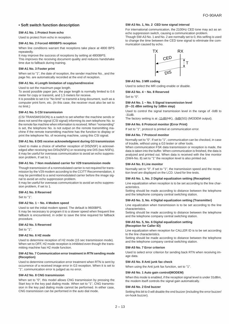
• Soft switch function description
SW-A1 No. 1 Protect from echo
Used to protect from echo in reception.
SW-A1 No. 2 Forced 4800BPS reception
When line conditions warrant that receptions take place at 4800 BPSrepeatedly.It may improve the success of receptions by setting at 4800BPS.This improves the receiving document quality and reduces handshaketime due to fallback during training.
SW-A1 No. 3 Footer print
When set to "1", the date of reception, the sender machine No., and thepage No. are automatically recorded at the end of reception.
SW-A1 No. 4 Length limitation of copy/send/receive
Used to set the maximum page length.To avoid possible paper jam, the page length is normally limited to 0.6meter for copy or transmit, and 1.5 meters for receive.It is possible to set it to "No limit" to transmit a long document, such as acomputer print form, etc. (In this case, the receiver must also be set tono limit.)
SW-A1 No. 5 CSI transmission
(CSI TRANSMISSION) is a switch to set whether the machine sends ordoes not send the signal (CSI signal) informing its own telephone No. tothe remote fax machine when information is received. When "nonsending"is set, the telephone No. is not output on the remote transmitting ma-chine if the remote transmitting machine has the function to display orprint the telephone No. of receiving machine, using this CSI signal.
SW-A1 No. 6 DIS receive acknowledgment during G3 transmission
Used to make a choice of whether reception of DIS(NSF) is acknowl-edged after receiving two DISs(NSFs) or receiving one DIS (two NSFs).It may be useful for overseas communication to avoid an echo suppres-sion problem, if set to 1.
SW-A1 No. 7 Non modulated carrier for V29 transmission mode
Though transmission of a nonmodulated carrier is not required for trans-mission by the V29 modem according to the CCITT Recommendation, itmay be permitted to a send nonmodulated carrier before the image sig-nal to avoid an echo suppression problem.It may be useful for overseas communication to avoid an echo suppres-sion problem, if set to 1.
SW-A1 No. 8 Reserved
Set to "1".
SW-A2 No. 1 ~ No. 4 Modem speed
Used to set the initial modem speed. The default is 9600BPS.It may be necessary to program it to a slower speed when frequent linefallback is encountered, in order to save the time required for fallbackprocedure.
SW-A2 No. 5 Reserved
Set to "1".
SW-A2 No. 6 H2 mode
Used to determine reception of H2 mode (15 sec transmission mode).When set to OFF, H2 mode reception is inhibited even though the trans-mitting machine has H2 mode function.
SW-A2 No. 7 Communication error treatment in RTN sending mode(Reception)
Used to determine communication error treatment when RTN is sent byoccurrence of a received image error in G3 reception. When it is set to"1", communication error is judged as no error.
SW-A2 No. 8 CNG transmission
When set to "0", this model allows CNG transmission by pressing theStart key in the key pad dialing mode. When set to "1", CNG transmis-sion in the key pad dialing mode cannot be performed. In either case,CNG transmission can be performed in the auto dial mode.
2 – 13
TX RX
CED
DIS
T
SW-A3 No. 1, No. 2 CED tone signal interval
For international communication, the 2100Hz CED tone may act as anecho suppression switch, causing a communication problem.Though SW-A3 No. 1 and No. 2 are normally set to 0, this selfing is usedto change the time between the CED tone signal to eliminate the com-munication caused by echo.
SW-A3 No. 3 MR coding
Used to select the MR coding enable or disable.
SW-A3 No. 4 ~ No. 8 Reserved
Set to "0".
SW-A4 No. 1 ~ No. 5 Signal transmission level(0~-31 dBm setting by 1dBm step)
Used to control the signal transmission level in the range of -0dB to-31dB.The factory setting is at -11dB(HK), -9dB(SG) (MODEM output).
SW-A4 No. 6 Protocol monitor (Error Print)
If set to "1", protocol is printed at communication error.
SW-A4 No. 7 Protocol monitor
Normally set to "0". If set to "1", communication can be checked, in caseof trouble, without using a G3 tester or other tools.When communication FSK data transmission or reception is made, thedata is taken into the buffer. When communication is finished, the data isanalyzed and printed out. When data is received with the line monitor(SW4-No. 8) set to "1" the reception level is also printed out.
SW-A4 No. 8 Line monitor
Normally set to "0". If set to "1", the transmission speed and the recep-tion level are displayed on the LCD. Used for line tests.
SW-A5 No. 1, No. 2 Digital equalization setting (Reception)
Line equalization when reception is to be set according to the line char-acteristics.Setting should be made according to distance between the telephoneand the telephone company central switching station.
SW-A5 No. 3, No. 4 Digital equalization setting (Transmitter)
Line equalization when transmission is to be set according to the linecharacteristics.Setting should be made according to distance between the telephoneand the telephone company central switching station.
SW-A5 No. 5, No. 6 Digital equalization setting(Reception for Caller ID)
Line equalization when reception for CALLER ID is to be set accordingto the line characteristics.Setting should be made according to distance between the telephoneand the telephone company central switching station.
SW-A5 No. 7 Error criterion
Used to select error criterion for sending back RTN when receiving im-age data.
SW-A5 No. 8 Anti junk fax check
When using the Anti junk fax function, set to "1".
SW-A6 No. 1 Auto gain control(MODEM)
When this mode is enabled, if the reception signal level is under 31dBm,the modem itself controls the signal gain automatically.
SW-A6 No. 2 End buzzer
Setting this bit to 0 will disable the end buzzer (including the error buzzer/on-hook buzzer).

FO-90AAR
No. 1 No. 2 No. 3
0 0 0 1.7sec
0 0 1 2.0sec
0 1 0 2.5sec
0 1 1 3.0sec
1 0 0 3.6sec
1 0 1 4.0sec
1 1 0 5.5sec
1 1 1 7.0sec
SW-A6 No. 3 Disconnect the line when DIS is received in RX mode
Bit1 = 0 : When DIS signal is received during RX mode, disconnect theline immediately.
Bit1 = 1 : When DIS signal is received during RX mode, wait for the nextsignal.
SW-A6 No. 4 Equalizer freeze control (MODEM)
This switch is used to perform reception operation by fixing the equal-izer control of modem for the line which is always in unfavorable stateand picture cannot be received.* Usually, the control is executed according to the state of line where theequalizer setting is changed always.
SW-A6 No.5 Equalizer freeze 7200BPS only
Setting which specifies SW-A6 No. 4 control only in condition of 7200BPSmodem speed.
SW-A6 No. 6 CNG transmission in manual TX mode
When set to "1", fax transmit the CNG signal in case of manualtransmissiom mode (User press the START key after waiting for the faxanswering signal from handset or speaker).
SW-A6 No. 7 Initial compression scheme for sharp fax in TX mode
When set to "0", if the other fax is Sharp model, fax transmit the docu-ment by H2 mode.When set to "1", even if the other fax is Sharp model, fax transmit thedocument by MR mode.
SW-A6 No. 8 Modem speed automatic down when RX level is under-40dBm
When set to "1", if fax signal level is under -40dBm during reception,machine selects the slower modem speed automatically.It is effective when noises occur on the received document due to thelong distance communications.
SW-A7 No. 1, No. 2 EOL (End Of Line) detect timer
Used to make a choice of whether to use the 5 or 13 or 20 or 25 secondstimer for detection of EOL.This is effective to override communication failures with some facsimilemodels that have longer EOL detection.
SW-A7 No. 3 ~ No. 8 Reserved
Set to "0".
SW-B1 No. 1 Hold key
Used to set YES/NO of holding function by the HOLD key.
SW-B1 No. 2 Auto dial fax transmission by REDIAL key
When set to "1", if original documents are set to the feeder and youpress REDIAL key, machine will dial and transmit the ducuments auto-matically.When set to "0", operator needs to press the START key after FAX re-ception tone is heard.
SW-B1 No. 3 Reserved
Set to "0".
SW-B1 No. 4 ~ No. 8 Recall interval(0~15.5min setting by 0.5min step)
Choice is made for a redial interval for speed and rapid dial calls.Use a binary number to program this with 0.5min steps. If set to 0 acci-dentally, 0.5min will be assumed.
SW-B2 No. 1 ~ No.4 Recall times (0~15times setting)
Choice is made as to how many redials there should be.
SW-B2 No. 5 Dial tone detection (Before auto dial)
Used to set YES/NO of dial tone detection in auto dialing.
SW-B2 No. 6 Reserved
Set to "0".
SW-B2 No. 7 Busy tone detection (After auto dial)
Used to set YES/NO of busy tone detection after auto dialing.
SW-B2 No. 8 Busy tone detection pulse number (After auto dial)
Used for detection of busy tone in 2 or 4 pulses.
SW-B3 No. 1, No. 2 Waiting time after dialing
This is waiting time for the opponent's signals after dialing.45 / 55 / 90 / 140 seconds settings are available.
SW-B3 No. 3 ~ No. 8 Reserved
Set to "0".
SW-B4 No. 1 Dialing pause (sec/pause)
Pauses can be inserted between telephone numbers of direct dial con-nection. Selection of 4 sec or 2 sec pause is available.
SW-B4 No. 2 Dial mode
When using the pulse dial, set to 0. When using the tone dial, set to 1.
SW-B4 No. 3 Pulse → Tone change function by key
When setting to 1, the mode is changed by pressing the key from thepulse dial mode to the tone dial mode.
SW-B4 No. 4 Dial pulse make/break ratio (%)
When using the 33% make ratio pulse dial, set to 0.When using the 40% make ratio pulse dial, set to 1.
SW-B4 No. 5, No. 6 Auto dial mode Delay timer of before line con-nect
Delay time between the dial key input and line connection under theauto dial mode.
2 – 14
RAPID A CML RELAY ON
DIALLING
No.5=0 No.6=0 : 0secNo.5=0 No.6=1 : 1.5secNo.5=1 No.6=0 : 3.0secNo.5=1 No.6=1 : 4.5sec
RAPID A CML RELAY ONDIAL DATA
SW-B4 No. 7, No. 8 Reserved
Set to "0".
SW-B5 No. 1 ~ No. 3 Auto dial mode Delay timer of after line con-nect
Delay time between the line connection and dial data output under theauto dial mode.This setting is available when dial tone detection(SW-B2 No. 5) is set to"NO".
SW-B5 No. 4 Fax signal detects after telephone mode dial
When set to "1", if machine detects the fax answering signal after tel-ephone calling (handset off-hook or speaker mode dial), machine startsto receive the documents automatically.

FO-90AAR
2 – 15
SW-B5 No. 5 Recalling fixed only one time when dialing was un-successful without detecting busy tone signal
When set to "1", if machine does not detect the busy tone after autodialing and dialing is unsuccessful, machine will try to recall only onetime.
SW-B5 No. 6 ~ No. 8 Reserved
Set to "0".
SW-B6 No. 1 ~ No. 5 DTMF signal transmission level(Low frequency 0~15.5dBm setting by 0.5dBm step)
The transmission level of DTMF signal is adjusted. (lower frequency)
00000: 0dBm
↓
11111: -15.5 dBm (-0.5dBm x 31)
SW-B6 No. 6 ~ No. 8 Reserved
Set to "0".
SW-B7 No. 1 ~ No. 5 DTMF signal transmission level(High frequency 0~15.5dBm setting by 0.5dBm step)
The transmission level of DTMF signal is adjusted. (higher frequency)
00000: 0dBm
↓
11111: -15.5 dBm (-0.5dBm x 31)
SW-B7 No. 6 ~ No. 8 Reserved
Set to "0".
SW-C1 No. 1, No. 2 Reading slice (Binary)
Used to determine the set value of reading density in standard/fine/su-per-fine mode.The standard setting is "00"(Factory setting is "00").
SW-C1 No. 3, No. 4 Reading slice (Half tone)
Used to determine the set value of reading density in half tone mode.The standard setting is "00"(Factory setting is "00").
SW-C1 No. 5 Line density selection
Used to set the transmission mode which is automatically selected whenthe Resolution key is not pressed. In the copy mode, however, the finemode is automatically selected unless the Resolution key is manuallyset to another mode.
SW-C1 No. 6 Reserved
Set to "0".
SW-C1 No. 7 MTF correction in half tone mode
This allows selection of MTF correction (dimness correction) in the halftone mode.When "NO" (=1) is selected, the whole image becomes soft and mild.Clearness of characters will be reduced. Normally set to "YES" (=0).
SW-C1 No. 8 Reserved
Set to "0".
SW-D1 No.1 ~ No. 4 Number of rings for auto receive(0~15rings setting)
When the machine is set in the auto receive mode, the number of ringsbefore answering can be selected. It may be set from one to nine ringsusing a binary number. Since the facsimile telephone could be used asan ordinary telephone if the handset is taken off the hook, it should beprogrammed to the user's choice. If the soft switch was set to 1, directconnection is made to the facsimile.If a facsimile calling beep was heard when the handset is taken off thehook, press the START key and put the handset on the hook to have thefacsimile start receiving. If it was set to 0 accidentally, receive ring is setto 1.
NOTE: If the machine is set to answer after a large number of rings, itmay not be able to receive faxes successfully.If you have difficulty receiving faxes, reduce the number of ringsto a maximum of 5.
SW-D1 No. 5 Automatic switching manual to auto receive function
This soft switch is used to select whether the machine should switch tothe auto receive mode after 5 rings in the manual receive mode or re-main in the same way as SW-D1 No. 1, No. 2, No. 3 and No. 4 "0"1"0"1"(5rings).
SW-D1 No. 6, No. 7 CI detect frequency
Detection frequency of ring signal for auto reception is set.
When set to No. 6=0, No. 7=0, frequency is set to PTT recommendation.When set to No. 6=0, No. 7=1, frequency is set to 11.5Hz or more.When set to No. 6=1, No. 7=0, frequency is set to 13.0Hz or more.When set to No. 6=1, No. 7=1, frequency is set to 20.0Hz or more.
SW-D1 No. 8 Reserved
Set to "0".
SW-D2 No. 1 ~ No. 5 Reserved
Set to "0".
SW-D2 No. 6 Caller ID Function
Used for Caller ID function.
SW-D2 No. 7, No. 8 Reserved
Set to "0".
SW-D3 No. 1 ~ No. 5 CI off detection timer(0~1550ms setting by 50ms step)
Set the minimum time period of CI signal interruption which affords to bejudged as a CI OFF section with 50ms steps.(Example)
A B
400msec 2000msec1 2
0 1 1 1 0 (50ms~14) : 700ms(CI interruption>700ms:Judged as a CIOFF section)The section 1 is not judged as a CI OFF sec-tion, the CI signal A is counted as one signal.The section 2 is judged as a CI OFF section,the CI signal B is considered as the second sig-nal.
0 0 1 1 1 (50ms~7) : 350ms(CI interruption>350ms:J udged as a CIOFF section)The section 1 is judged as a CI OFF section,and the CI signal A is counted as two signals.The section 2 is judged as a CI OFF section,and the CI signal B is considered as the thirdsignal.
SW-D3 No. 6 ~ No. 8 Reserved
Set to "0".
SW-D4 No. 1 ~ No. 6 DTMF type Caller ID RX level(0~-44dBm setting by 1dBm step)
This is used for DTMF type Caller ID detection level setting.
SW-D4 No. 7, No. 8 Reserved
Set to "0".
SW-E1 No. 1 ~ No. 3 Pseudo ringing time at the TEL/FAX automaticswitching mode
Choice is made as to how long to rumble the dummy ringer on TEL/FAXautomatic switching mode.
SW-E1 No. 4 Number of CNG signal detection at the TEL/FAX auto-matic switching mode
Used for detection of CNG in one tone or two tones in the TEL/FAXautomatic switching mode.

FO-90AAR
2 – 16
SW-E1 No. 5 CNG detect time at TEL/FAX mode
The switch which sets the time from the start of CNG detection to theend of detection.
SW-E1 No. 6 Post answer tone (TEL/FAX mode)
When set to "0", machine send the tones in TEL/FAX auto changeovermode.
SW-E1 No. 7 Type of post answer tone
When set to "0", post answer tone is 800Hz single tone.When set to "1", post answer tone is 880Hz/988Hz/1046Hz(LA-SI-DO)tone.
SW-E1 No. 8 Pseudo ringer ON/OFF cycle
When set to "0", pseudo ringer is 1 sec ON and 2 sec OFF cycles.When set to "1", pseudo ringer is 1 sec ON and 4 sec OFF cycles.
SW-E2 No. 1 ~ No. 4 Pseudo ringer sound output level to the line(0~-15dBm setting by 1dBm step)
Used to adjust the sound volume of pseudo ringer to the line (ring backtone) generated on selecting TEL/FAX.
SW-E2 No. 5 ~ No. 8 Post answer tone transmission level(0~-15dBm setting by 1dBm step)
Used to adjust the sound volume of post answer tone to the line gener-ated on selecting TEL/FAX.
SW-E3 No. 1 Reserved
Set to "0"
SW-E3 No. 2, No. 3 Action select when DTMF "#" is received duringphone/fax automatic switching mode
SW-E3 No. 4 ~ No. 8 Reserved
Set to "0".
SW-F1 No. 1, No. 2 DTMF detection time
Used to set detect time of DTMF (Dual Tone Multi Frequency) used inremote reception(5 ).The longer the detect time is, the less the error detection is caused bynoises.
SW-F1 No. 3 Protection of remote reception (5 ) detection
Used to set the function of remote reception (5 ). When set to "1",the remote reception function is disabled.
SW-F1 No. 4 Remote reception with GE telephone
"1": Compatible with TEL mode by GE
"0": Not compatible
• When sending (5 ) for remote reception with a GE manufacturedtelephone remote reception may not take place because of specialspecifications in their DTMF.
To overcome this, a soft SW is provided to change the modem settingto allow for remote reception.
• If this soft SW is set to "1", other telephone sets may be adverselyaffected.
SW-F1 No. 5 ~ No. 8 Remote operation code figure by external TEL(0~9)
Remote operation codes can be changed from 0 through 9. If set togreater than 9, it defaults to 9. The "5 " is not changed.Ex- 7 (Default : 5 )
SW-F2 No. 1 CNG detection in STAND-BY mode
When setting to "1", the CNG signal detection function during standbystops.
SW-F2 No. 2, No. 3 Number of CNG detect (AM mode)
Used for detection of CNG in 1 to 4 pulses.
SW-F2 No. 4, No. 5 Number of CNG detect (STAND-BY mode)
Used for detection of CNG in 1 to 4 pulses.
SW-F2 No. 6 ~ No. 8 Reserved
Set to "0"
SW-G1 No. 1 ~ No. 8 Reserved
Set to "0"
SW-G2 No. 1 ~ No. 8 Reserved
Set to "0"
SW-G3 No. 1 ~ No. 8 Reserved
Set to "0"
SW-G4 No. 1 ~ No. 6 Quiet detect level setting(0~-44dBm setting by 1dBm step)
This is used to change the quiet detect level setting.
If quiet detection is difficult due to noise, reduce this setting level.
(Example)
Factory setting : 1 0 1 1 0 0 (- 44dBm)
↓
1 0 1 0 0 0 (- 40dBm)
SW-G4 No. 7 Fax switching when A.M. full
If the answering machine’s memory (tape) is full and there is no response,the machine automatically switches to Fax reception.
SW-G4 No. 8 Reserved
Set to "0".
SW-H1 No. 1 Busy tone continuous sound detect time
Set detecting time busy tone for 5 seconds or 10 seconds.
SW-H1 No. 2 Busy tone detect continuation sound detect duringOGM
Used to detect the continuous tone of specific frequency during OGMoutput.
SW-H1 No. 3 Busy tone detect continuation sound detect
Used to select detection of the continuous sound of certain frequency.
SW-H1 No. 4 Busy tone detect intermittent sound detect during OGM
Used to detect the intermittent tone of specific frequency during OGMoutput.
SW-H1 No. 5 Busy tone detect intermittent sound detect
Used to select detection of the intermittent sound of certain frequency.
SW-H1 No. 6, No. 7 Busy tone detection pulse number
Used to set detection of Busy tone intermittent sounds.
SW-H1 No. 8 Reserved
Set to "0".
SW-H2 No. 1, No. 2 Busy tone detection ON/OFF time(Lower duration)
The initial value of detection is set according to electric condition.
The set value is changed according to the local switch board. (Erro-neous detection of sound is reduced.)
If erroneous detection is caused by sound, etc., adjust the detectionrange.
The lower limit can be set in the range of 150msec to 350msec.
SW-H2 No. 3, No. 4 Busy tone detection ON/OFF time(Upper duration)
Similarly to SW-H1 No. 1, the set value can be varied.
The upper limit can be set in the range of 650msec to 2700msec.
SW-H2 No. 5 Busy tone continuation sound detect frequency
Set detecting frequency of busy tone continuation sound for 320 ~ 570Hz of 320 ~ 460 Hz.
SW-H2 No. 6 ~ No. 8 Reserved
Set to "0".

FO-90AAR
2 – 17
SW-I1 No. 1, No. 2 ICM recording time
Used to select the incoming message recording time among 15sec/30sec/60sec/4min.
SW-I1 No. 3, No. 4 A.M. quiet time 1
Used to select four kinds of no sound time (2 sec ~ 5 sec) after receptionin the T.A.D mode until OGM is output.
Reception OGM output ICM recording
2 sec~ 5 sec ( SW-I1No. 3, No. 4)
Reception OGM output ICM recording
0 sec~3 sec (SW-I1 No. 5, No. 6)SW-I1 No. 7 key input buzzer on/off switch (Two way recording mode)
Used to turn ON/OFF key input buzzer in the TWO-WAY recording mode.
SW-I1 No. 8 Reserved
Set to "0".
SW-I2 No. 1 ~ No. 5 A.M. quiet detect time
Used to set no sound time (0 sec - 32 sec) during the T.A.D. mode op-eration.
SW-I2 No. 6 ~ No. 8 Reserved
Set to "0".
SW-I3 No. 1 Reserved
Set to "0".
SW-I3 No. 2 Max OGM record time
Used to select the maximum OGM recording time (1=15sec, 0=60sec).
SW-I3 No. 3 Two way record function
If this switch is set to "1", machine doesn’t work two way recording func-tion.
SW-I3 No. 4 Toll saver
Used to turn on the toll saver function. If it is off, the reception frequencyin the AM mode is indentical with that in the FAX mode.
SW-I3 No. 5 FAX reception in case of detecting no sound detectafter ICM recording
If this switch is set to "0", machine doesn’t change to FAX receptionmode when detect no sound in ICM recording.
SW-I3 No. 6, No. 7 Reserved
Set to "0".
SW-I3 No. 8 Transfer dial recall
If this switch is set to "1", machine disable redial in Transfer function.
SW-I4 No. 1 ~ No. 4 AGC maximum gain (Line)(10~25dB) (1 dB step)
The AGC Maximum Gain limits the gain applied by the AGC. Messagewith average energy below the AGC Energy Reference Level will havetheir average energy level increased by no more than the AGC Maxi-mum Gain. The AGC Maximum Gain should average energy of the mes-sage with the lowest average energy to the AGC Energy Reference Level.
SW-I4 No. 5 ~ No. 8 AGC maximum gain (Mic)(10~25dB) (1 dB step)
The AGC Maximum Gain limits the gain applied by the AGC. Messagewith average energy below the AGC Energy Reference Level will havetheir average energy level increased by no more than the AGC Maxi-mum Gain. The AGC Maximum Gain should average energy of the mes-sage with the lowest average energy to the AGC Energy Reference Level.
SW-I5 No. 1 ~ No. 4 AGC eref access code (Line)(-0~-30dB) (2 dB step)
The AGC Energy Reference Level controls the playback level. Any mes-sage having average speech energy above the energy reference levelhas its playback level attenuated, and any level has its playback levelincreased. If the playback level is too high (low), then decreasing (in-creasing) the AGC energy Reference level will achieve the desired level.
SW-I5 No. 5 ~ No. 8 AGC eref access code (Mic)(-0~-30dB) (2 dB step)
The AGC Energy Reference Level controls the playback level. Any mes-sage having average speech energy above the energy reference levelhas its playback level attenuated, and any level has its playback levelincreased. If the playback level is too high (low), then decreasing (in-creasing) the AGC energy Reference level will achieve the desired level.
SW-I6 No. 1 ~ No. 4 AGC gain adaptation threshold (Line)
The AGC adjusts the amount of gain applied to the incoming messageonly when the average energy exceeds the AGC Gain Adaptation Thresh-old. The AGC Gain Adaptation Threshold prevents message backgroundnoise from corrupting the gain provided that the AGC Gain AdaptationThreshold is greater than the background noise energy. In the event thata message has background noise energy greater than the AGC GainAdaptation Threshold, the AGC Gain can be no greater than the AGCMaximum Gain. Note that the AGC Gain Adaptation Threshold must al-ways be greater than the RPACS VOX Turn-On Threshold.
SW-I6 No. 5 ~ No. 8 AGC gain adaptation threshold (Mic)
The AGC adjusts the amount of gain applied to the incoming messageonly when the average energy exceeds the AGC Gain Adaptation Thresh-old. The AGC Gain Adaptation Threshold prevents message backgroundnoise from corrupting the gain provided that the AGC Gain AdaptationThreshold is greater than the background noise energy. In the event thata message has background noise energy greater than the AGC GainAdaptation Threshold, the AGC Gain can be no greater than the AGCMaximum Gain. Note that the AGC Gain Adaptation Threshold must al-ways be greater than the RPACS VOX Turn-On Threshold.
SW-I7 No. 1, No. 2 AGC slew rate (Line)
The AGC Slew Rate controls the convergence of the message playbacklevel to the desired playback level. A large slew rate will allow fasterconvergence and a small slew rate will allow slower convergence.
SW-I7 No. 3, No. 4 AGC slew rate (Mic)
The AGC Slew Rate controls the convergence of the message playbacklevel to the desired playback level. A large slew rate will allow fasterconvergence and a small slew rate will allow slower convergence.
SW-I7 No. 5 ~ No. 8 Reserved
Set to "0".
SW-I8 No. 1 ~ No. 5 OGM/ICM output level
Used to control OGM and ICM output level.
SW-I8 No. 6 AM OGM announce only mode
If this switch is set to 1, the machine is not recording ICM.(disconnect the line after OGM output)
SW-I8 No. 7, No. 8 Reserved
Set to "0".
SW-J1 No. 1 Sender's phone number setting
Used to make a choice of whether the registered sender's phone numbercan be changed or not. If the switch is set to "1", new registration of thesender's phone number is disabled to prevent accidental wrong input.
SW-J1 No. 2 Reserved
Set to "1".
SW-J1 No. 3, No. 4 Ringer Volume
Used to adjust ringing volume.
SW-J1 No. 5, No. 6 Reserved
Set to "0".
SW-I1 No. 5, No. 6 A.M. quiet time 2
Used to select four kinds of no sound time (0 sec ~ 3 sec) after OGMoutput the T.A.D mode until ICM recording is started.

FO-90AAR
2 – 18
SW-J1 No. 7 Polling key
If this switch is set to 1, the last of Rapid key works as polling key.
SW-J1 No. 8 Reserved
Set to "0".
SW-J2 No. 1, No. 2 Reserved
Set to "0".
SW-J2 No. 3 ~ No. 5 Speaker Volume
Used to adjust sound volume from a speaker.
SW-J2 No. 6 Reserved
Set to "0".
SW-J2 No. 7 Saving energy start timing
Used to set the time between the machine’s stand-by state (clock indi-cation) after operation and saving energy mode.It is possible to set the time to either 5 sec or 180 sec (default).
SW-J2 No. 8 Saving energy mode
Used to select whether to make the saving energy mode valid or not.
SW-J3 No. 1 ~ No. 3 Communication results printout(Transaction report)
It is possible to obtain transaction results after each communication.Normally,the switch is set (No. 1 : 0, No. 2 : 0, No. 3 : 0) so that thetransaction report is produced only when a communication error is en-countered.If No.1 was set to 0 and No. 2 to 1 and No. 3 to 0, the transaction reportwill be produced every time a communicaion is done, even if thecommunicaion was successful.Setting No. 1 to 0 and No. 2 to 1 and No. 3 to 1 will disable this function.No transaction report printed.
SW-J3 No. 4 Time format
When set to "0", 24hour time format is used.When set to "1", 12hour time format is used.
SW-J3 No. 5 Date format
When set to "0", Day-Month-Year format is used.When set to "1", Month-Day-Year format is used.
SW-J3 No. 6 ~ No. 8 Reserved
Set to "0".
SW-K1 No. 1 Entering diag mode by pressing SPEED key
A bit which is used in the production process only. When the SPEED keyis pressed, the switch is changed from the stand-by state to the diagmode.
SW-K1 No. 2 ~ No. 8 Reserved
Set to "0".

FO-90AAR
2 – 19
[3] Troubleshooting
Refer to the following actions to troubleshoot any of the problems men-tioned in 1-4.
[1] A communication error occurs.
[2] Image distortion produced.
[3] Unable to do overseas communication.
[4] Communication speed slow due to FALLBACK.
• Increase the transmission level SOFT SWITCH A4-1, 2, 3, 4, 5.May be used in case [1] [2] [3].
• Decrease the transmission level SOFT SWITCH A4-1, 2, 3, 4,5. May be used in case [3].
• Apply line equalization SOFT SWITCH A5-1, 2.May be used in case [1] [2] [3] [4].
• Slow down the transmission speed SOFT SWITCH A2-1, 2, 3,4. May be used in case [2] [3].
• Replace the TEL/LIU PWB.May be used in all cases.
• Replace the control PWB.May be used in all cases.
* If transmission problems still exist on the machine, use the followingformat and check the related matters.
TO: ATT: Ref.No. :
CC: ATT: Date :
FM: Dept :
Sign :
* Please complete this report before calling the “TAC” hotline if problem still occurs.
***** Facsimile communication problem ***** Ref.No.:
Date:From: Mr. Fax Tel No.:Our customer Name Tel No.
Address Fax No.
Contact person Model name
Other party Name Tel No.Address Fax No.Contact person Model name
Problem mode Line: Domestic / international Model: G3 Phase: A, B, C, D.
Reception / TransmissionAutomatic reception / Manual receptionAutomatic dialing / Manual dialing / Others
Frequency: % ROM version:
Confirmationitem
Please mark problem with an X.No problem is: 0.
A1 A2 B1 B2 C1 C2 D1 D2 E1 E2
Transmission level setting is ( ) dB at ourcustomer
Transmission level ( ) dBmReception level ( ) dBmBy level meter at B1 and B2
Comment
**** Please attach the G3 data and activity report on problem. ****
Countermeasure
Our customer
Our service
A1 A2 C1 D2
B1B2
E1E2
C2 D1
Other party
Other party's service

FO-90AAR
[4] Error code table
1. Communication error code table
G3 TransmissionCode Final received signal Error Condition (Receiver side)
0 Incomplete signal frame Cannot recognize bit stream after flag
1 NSF, DIS Cannot recognize DCS signal by echo etc.
Cannot recognize NSS signal (FIF code etc)
2 CFR Disconnects line during reception (carrier missing etc)
3 FTT Disconnects line by fall back
4 MCF Disconnects line during reception of multi page
Cannot recognize NSS, DCS signal in the case of mode change
5 PIP or PIN The line is hung up without replying to telephone request from the receiving party.
6 RTN or RTP Cannot recognize NSS, DCS signal after transmit RTN or RTP signal.
7 No signal or DCN No response in receiver side or DCN signal received* (transmitter side)
8 − Owing to error in some page the error could not be corrected although the specified number of
error retransmissions were attempted.
11 − Error occurred after or while reception by the remote (receiving) machine was revealed to be
impossible.
12 − Error occurred just after fallback.
13 − Error occurred after a response to retransmission end command was received.
G3 Reception
Code Final received signal Error Condition (Receiver side)
0 Incomplete signal frame Cannot recognize bit stream after flag
1 NSS, DCS Cannot recognize CFR or FTT signal
Disconnects line during transmission (line error)
2 NSC, DTC Cannot recognize NSS signal (FIF code etc)
3 EOP Cannot recognize MCF, PIP, PIN, RTN, RTP signal
4 EOM Cannot recognize MCF, PIP, PIN, RTN, RTP signal in the case of mode change
5 MPS The line is hung up without replying to communication request.
6 PR1-Q Cannot recognize PIP, PIN signal in the case of TALK request
7 No signal or DCN No response in transmitter (cannot recognize DIS signal) or DCN signal received* (receiver side)
8 − Error occurred upon completion of reception of all pages.
9 − Error occurred when mode was changed or Transmission/Reception switching was performed.
10 − Error occurred during partial page or physical page reception.
11 − Error occurred after or during inquiry from the remote (transmitting) machine as to whether
reception is possible or not.
12 − Error occurred during or just after fallback.
13 − Error occurred after the retransmission end command was received.
2 – 20

FO-90AAR
2 – 21
M E M O
FO-90AAR
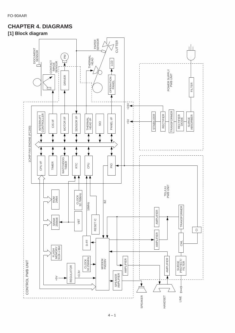
4 – 1
[1] Block diagramCHAPTER 4. DIAGRAMS
SR
AM
256k
bit
RO
M2M
bit
CP
U
CP
U I/
F
TIM
ER
RT
C
PIO
WA
TC
HD
OG
TIM
ER
CLO
CK
32.7
68kH
z
INT
ER
RU
PT
CO
NT
RO
LLE
R
CIS
I/F
MO
TO
R I/
F
SE
NS
OR
I/F
SIO
TH
ER
MA
LH
EA
D I/
F
PA
NE
L I/F
PM
OP
ER
AT
ION
PA
NE
L
CO
NT
RO
L P
WB
UN
IT1C
HIP
FA
X E
NG
INE
(F
C20
0)
HA
ND
SE
T
SP
EA
KE
R
+5V
+24
V
OP
ER
AT
ION
PA
NE
L
TE
L/LI
UP
WB
UN
IT
DR
IVE
R
TH
ER
MA
LH
EA
DPM
CO
NT
AC
TIM
AG
ES
EN
SO
RDO
CU
ME
NT
SE
NS
OR
PO
WE
R S
UP
PLY
PW
B U
NIT
ST
AB
ILIZ
ER
MO
DE
MF
M20
9V
AM
PLI
FIE
R
AM
PLI
FIE
R
SU
RG
EP
RO
TE
CT
/F
ILT
ER
CM
LT
RA
NS
FO
RM
ER
CI
VB
T
RE
CT
IFIE
R
TR
AN
SF
OR
ME
R
RE
CT
IFIE
RD
IOD
E
TR
AN
SS
UR
GE
AB
SO
RB
ER
FIL
TE
R
LIN
E
PA
PE
RS
EN
SO
RR
ES
ET
IC
AM
PLI
FIE
R
BZ
CLO
CK
32.2
56M
Hz
LCD
D-F
F16
MH
z
+3.
3V
+5V
RE
GU
LAT
OR
CU
TT
ER
AM
PLI
FIE
R
FLA
SH
ME
MO
RY
512k
x 8
bit
SP
EA
KE
RA
MP
LIF
IER
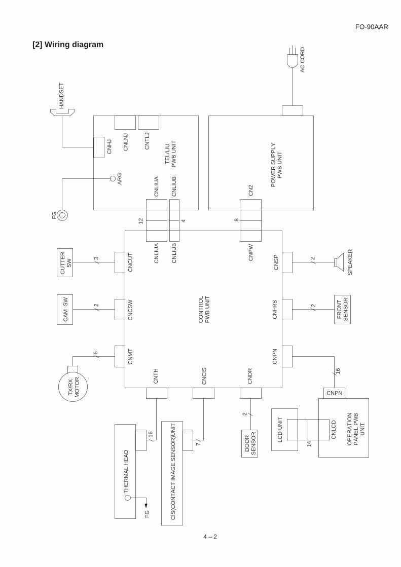
FO-90AAR
[2] Wiring diagram
4 – 2
CN
CIS
CN
DR
CN
TH
DO
OR
SE
NS
OR
CN
PW
CN
2
CN
LIU
A
CN
LNJ
812
CN
LIU
A
CN
FR
S
FR
ON
TS
EN
SO
R
CN
SP
CN
CU
TC
NC
SW
CN
MT
CU
TT
ER
SW
CA
M S
WT
X/R
XM
OT
OR
62
3
22
CN
PN
SP
EA
KE
R
16
CNPN
CN
LCD
OP
ER
AT
ION
PA
NE
L P
WB
UN
IT
LCD
UN
IT
16
7
TH
ER
MA
L H
EA
D
CIS
(CO
NT
AC
T IM
AG
E S
EN
SO
R)U
NIT
HA
ND
SE
TF
G
AR
G
CN
HJ
TE
L/LI
UP
WB
UN
IT
PO
WE
R S
UP
PLY
PW
B U
NIT
CO
NT
RO
LP
WB
UN
IT
FG
14A
C C
OR
D
2
CN
TLJ
CN
LIU
BC
NLI
UB
4

FO-90AAR
[3] Point- to-point diagram
4 – 3
TX/RXMOTOR
TPADTPBDTPADTPBDVMTVMT
123456
123456789
10111213141516
123456789
10111213141516
123456789
10111213141516
123456789
10111213141516
123456
OPERATIONPANELPWB
TPADTPBDTPADTPBDVMTVMT
THERMALHEAD
VTHVTH
STRB1STRB2
THIN.C.MGMGMG+5V
STRB3STRB4LATCHPCLKDATAVTH
VTHVTH
STRB1STRB2
THIRANK
MGMGMG+5V
STRB3STRB4LATCHPCLKDATAVTH
1234567
1234567
VODG+5VøT
CISCLKGLED+24V
VODG+5VøT
CISCLKGLED+24V
DG+5V
SEN4E
SEN0SEN1SEN2SEN3SEN5SEN6SEN7
ORGSNSKEN4AKEN3AKEN2AKEN1A
DG+5V
SEN4E
SEN0SEN1SEN2SEN3SEN5SEN6SEN7
ORGSNSKEN4AKEN3AKEN2AKEN1A
CNPN CNPN
CNCIS
123456789
101112
123456789
101112
TEL/LIUPWB
TELOUTTELIN
TELMUTECIHS
RHSRXIN
TXOUTCML+5VDG
+24V
TELOUTTELIN
TELMUTECIHS
RHSRXIN
TXOUTCML+5VDG
+24V
CNLIUACNLIUACNMT
CNTH
12345678
12345678
POWERSUPPLY
PWB
DG+5VMGMG
+24V+24VDG
PSAVE
DG+5VMGMG
+24V+24VDG
PSAVE
CN2CNPW
CNCSW
CNSP
CIS
12
CSWDG
CAMSWITCH
12
12
12
SP+SP-
CSWDG
SP+SP-
SPEAKER
CONTROLPWB
CNFRS12
12
FRSNSDG
FRSNSDG
FRONTSENSOR
CNCUT
CNDR
1
2
CUT
DG
CUTTERSENSOR
12
123
12
DRSNSDG
CUTN.C.DG
DRSNSDG
DOORSENSOR
1234
1234
N.C.N.C.
DPONDPMUTE
RLYCNTTXMUTE
DPONDPMUTE
CNLIUBCNLIUB

FO-90AAR
CHAPTER 5. CIRCUIT DESCRIPTION
[1] Circuit description
1. General descriptionThe compact design of the control PWB is obtained by using CONEXANTfax engine in the main control section and high density printing of sur-face mounting parts. Each PWB is independent according to its functionas shown in Fig. 1.
2. PWB configuration
Fig. 1
1) Control PWBThe control PWB controls peripheral PWBs, mechanical parts, trans-mission, and performs overall control of the unit.This machine employs a 1 chip modem (FM209V) which is installed onthe control PWB.
2) TEL/LIU PWBThis PWB controls connection of the telephone line to the unit.
3) Power supply PWBThis PWB provides voltages of +5V and +24V to the other PWBs.
4) Panel PWBThe panel PWB allows input of the operation keys.
5) LCD PWBThis PWB controls the LCD display.
3. Operational descriptionOperational descriptions are given below:
• Transmission operation
When a document is loaded in standby mode, the state of the docu-ment sensor is sensed via the 1 chip fax engine (FC200). If the sen-sor signal was on, the motor is started to bring the document into thestandby position. With depression of the START key in the off-hookstate, transmission takes place.Then, the procedure is sent out from the modem and the motor isrotated to move the document down to the scan line. In the scanprocessor, the signal scanned by the CIS is sent to the internal im-age processor and the AD converter to convert the analog signal intobinary data. This binary data is transferred from the scan processorto the image buffer within the RAM and encoded and stored in thetransmit buffer of the RAM. The data is then converted from parallelto serial form by the modem where the serial data is modulated andsent onto the line.
• Receive operation
There are two ways of starting reception, manual and automatic.Depression of the START key in the off-hook mode in the case ofmanual receive mode, or CI signal detection by the LIU in the auto-matic receive mode.
First, the FC200 controls the procedure signals from the modem tobe ready to receive data. When the program goes into phase C, theserial data from the modem is converted to parallel form in the mo-dem interface of the 1 chip fax engine (FC200) which is stored in thereceive buffer of the RAM. The data in the receive buffer is decodedsoftware-wise to reproduce it as binary image data in the image buffer.The data is DMA transferred to the recording processor within theFC200 which is then converted from parallel to serial form to be sentto the thermal head. The data is printed line by line by the FC200which is assigned to control the motor rotation and strobe signal.
• Copy operation
To make a copy on this facsimile, the COPY key is pressed when themachine is in stand-by with a document on the document table andthe telephone set is in the on-hook state.
First, depression of the COPY key advances the document to thescan line. Similar to the transmitting operation, the image signal fromthe CIS is converted to a binary signal in the DMA mode via the 1chip fax engine (FC200) which is then sent to the image buffer of theRAM. Next, the data is transferred to the recording processor in theDMA mode to send the image data to the thermal head which isprinted line by line. The copying takes place as the operation is re-peated.
5 – 1
LCDPWB
PANELPWB
CONTROLPWB
TEL/LIUPWB
POWERSUPPLYPWB
TX/RXMOTOR
AC CORD
CIS

FO-90AAR
[2] Circuit description of control PWB
1. General descriptionFig. 2 shows the functional blocks of the control PWB, which is com-posed of 5 blocks.
Fig. 2 Control PWB functional block diagram
2. Description of each block
(1) Main control blockThe main control block is composed of CONEXANT 1 chip fax engine(FC200), ROM (2Mbit), SRAM (256kbit), FLASH MEMORY (512k × 8bit) and Modem (FM209V).Devices are connected to the bus to control the whole unit.
1) FC200 (IC3) : pin-144 QFP (FAX ENGINE)
2) FM209V (IC5) : pin-128 QFP (MODEM)The FAX ENGINE Integrated Facsimile Controllers.
FC200, contains an internal 8 bit microprocessor with an external 16Mbyte address space and dedicated circuitry optimized for facsimileimage processing and facsimile machine control and monitoring.
3) 27C2000 (IC10): pin-32 DIP (ROM)ROM of 2 Mbit equipped with software for the main CPU.
4) W24258S-70LE (IC6): pin-28 SOP (SRAM)Line memory for the main CPU system RAM area and coding/decodingprocess. Used as the transmission buffer.
Memory of recorded data such as daily report and auto dials. When thepower is turned off, this memory is backed up by the lithium battery.
5) KM29W040T (IC4): pin-44 TSOP (FLASH MEMORY)A 512k × 8 bit NAND FLASH MEMORY to store the voice and imagedata when using memory functions.
Fig. 3
5 – 2
(1) FAX ENGINE
(3) ROM
(2) MODEM
(4) SRAM
MAIN CONTROL BLOCK
MODEM BLOCK
(5) FLASHMEMORY
MC24 CPU CONTROL IF
MC24 MEGACELL(8BIT DATA,24BIT ADDRESS)WATCHDOG TIMERREAL TIME CLOCK
CRYSTAL OSCILLATORBATTERY BACK-UP CIRCUITINTERRUPT CONTROLLER
BUS INTERFACE
DRAM CONTROLINTERNAL & EXTERNAL BUS CONTROL
INTERNAL & EXTERNAL DECODEDMA CONTROLLER
OPERATOR PANEL IF32 KEYS8 LEDS
LCD MODULEMOTOR POWER
CONTROL RINGERSYNC SERIF 1
THERMAL PRINTER IF
5 ms LINE TIMEA4/B4 LINES
TPH ADC4 STROBE TPH
LATCHLESS TPHEXTEMAL DMA I/F
T.4/T.6 CODEC
MH,MR,MMRHARDWARE,ALTERNATE
COMPRESSION &DECOMPRESSION
BI-LEVEL RESOLUTIONCONVERSION
PROGRAMMABLEREDUCTION &EXPANSION
2.6kBYTE VIDEO RAM
SCANNER CONTROL & VIDEO PROCESSING8-BIT PADC
CCD/CIS SCANNER5 ms,A4/B4 LINES
SHADING CORRECTION(1:1,1:8)DITHERING
MULTILEVEL B4-A4 REDUCTIONERROR DIFFUSION
MTF
GENERAL I/OTONE/ALTTONE
GPIOCALLING PARTY
CONTROLAUTOBAUD
SYNC-ASYNC SASIFSYNC SERIF 2
FLASH MEMORY IFAUTOBAUD
CPU BUS
INTERNAL CPU BUS
EXTERNAL CPU BUS
DMA BUS
WRPROTN
TSTCLKDEBUGNRESETNXINXOUTPWRDWNNBATRSTN
SYSCLK
SEE"OPIFOUTPUTS"BELOW
SEE"OPIFINPUTS"BELOW
THADIN
PDATPLATSTRB[3:0]STRBPOL
PCLK
PWR/GND TEST OPIF INPUTS
OPI[0]/GPIO[21]/SSRXD1OPI[1]/GPIO[22]/SSSTAT1OPI[2]/GPIO[23]/SSCLK1OPI[3]/GPIO[24]
OPIF OUTPUTS
LEDCTL/GPO[16]LCDCS/GPO[17]OPO[0]/GPO[8]/SINPWR CTRLOPO[1]/GPO[9]/PMPWR CTRLOPO[2]/GPO[10]/RINGEROPO[3]/GPO[11]OPO[4]/GPO[12]/SSTXD1OPO[5]/GPO[13]OPO[6]/GPO[14]OPO[7]/GPO[15]
ROMCSN
MCSNSYNC
REGDMAWAITNRASN
CASN[1:0]DWRN
CSN[1:0]
WRNRDN
D[7:0]A[23:0]MIRQN
TONE
VINCLK1CLK1N
CLK2VIDCTL0/FCS1NVIDCTL1/FCS2N
START –VREF+VREF
GPIO[0] GPIO[1]/SASTXD GPIO[2]/SASRXD GPIO[3]/SASCLK GPIO[4]/CPCIN GPIO[5]/SSCLK2 GPIO[6]/SSTXD2 GPIO[7]/SSRXD2 GPIO[8]/FWRN GPIO[9]/FRDN GPIO[10]/SSSTAT2 GPIO[11]/BE/SERINP GPIO[12]/CS2N GPIO[13]/CS3N GPIO[14]/CS4N GPIO[15]/CS5N GPIO[16]/IRQ8 GPIO[17]/IRQ5N GPIO[18]/IRQ9N GPIO[19]/RDY/SEROUT GPIO[20]/ALTTONESM[3:0]/GPO[7:4]PM[3:0]/GPO[3:0]

FO-90AAR
CPU Control InterfaceMIRQn 135 I HU − Modem interrupt, active low. (Hysteresis In, Internal Pullup.)SYSCLK 133 I H − System clock. (Hysteresis In.)TSTCLK 130 O − 123XT Test clock.
Bus Control InterfaceA[23:0] [1:6][8:13] O TU 123XT Address bus (24-bit).
[15:20][22:27]D[7:0] [136:139] I/O TU 123XT Data bus (8-bit).
[141:144]RDn 128 O − 123XT Read strobe.WRn 127 O − 123XT Write strobe.ROMCSn 120 O − 123XT ROM chip select.CS1n 122 O − 123XT I/O chip select.CS0n 57 O − 123XT SRAM chip select. (Battery powered.)MCSn 121 O − 123XT Modem chip select.SYNC 126 O − 123XT Indicates CPU op code fetch cycle (active high).REGDMA 124 O − 123XT Indicates REGSEL cycle and DMA cycle.WAITn 125 O − 123XT Indicates current TSTCLK cycle is a wait state or a halt state.RASn 113 O − 123XT DRAM row address select. (Battery powered.)CAS[1:0]n [111:112] O − 123XT DRAM column address select. (Battery powered.)DWRn 109 O − 123XT DRAM write. (Battery powered.)
Prime Power Reset Logic and TestDEBUGn 129 I HU − External non-maskable input (NMI).RESETn 131 I/O HU 2XO FC200 Reset.TEST 58 I C − Sets Test mode (Battery powered).
Battery Power Control and Reset LogicXIN 59 I OSC − Crystal oscillator input pin.XOUT 60 O − OSC Crystal oscillator output pin.PWRDWNn 62 I H − Used by external system to indicate -to FC200 - loss of prime power.
(Results in NMI)BATRSTn 61 I H − Battery power reset input.WRPROTn 110 O − 1XC (Battery powered.) Write protect during loss of VDD power.
NOTE:The functional logic is powered by battery power, but the output driveis powered by DRAM battery power.
Scanner InterfaceSTART 101 O − 2XS Scanner shift gate control.CLK1 100 O − 2XS Scanner clock.CLK1n 99 O − 2XS Scanner clock-inverted.CLK2 98 O − 2XS Scanner reset gate control (or clock for CIS scanner).FCS1n/VIDCTL0 96 O − 2XT Flash memory chip select or Video Control signal.FCS2n/VIDCTL1 97 O − 2XT Flash memory chip select or Video Control signal.
Printer InterfacePCLK/DMAACK 29 O − 3XC Thermal Print Head (TPH) clock, or external DMAACK.PDAT 30 O − 2XP Serial printing data (to TPH).PLAT 31 O − 3XP TPH data latch.STRB[3:0] [33:36] O − 1XP Strobe signals for the TPH.STRBPOL/DMAREQ 37 I C − Sets strobe polarity, active high/low or external DMA request.
Operator Panel InterfaceOPO[0]/GPO[8]/ 47 O − 2XL Keyboard/LED strobe [0] or GPO[8] or Scan Motor Power ControlSMPWRCTRLOPO[1]/GPO[9]/ 46 O − 2XL Keyboard/LED strobe [1] or GPO[9] or Print Motor Power ControlPMPWRCTRLOPO[2]/GPO[10]/ 44 O − 2XCT Keyboard/LED strobe [2] or GPO[10] or RINGERRINGEROPO[3]/GPO[11] 43 O − 2XL Keyboard/LED strobe [3] or GPO[11]OPO[4]/GPO[12]/ 42 O − 2XL Keyboard/LED strobe [4] or GPO[12] or SSTXD1 (for SSIF1)SSTXD1OPO[5]/GPO[13] 40 O − 2XL Keyboard/LED strobe [5] or GPO[13]OPO[6]/GPO[14] 39 O − 2XL Keyboard/LED strobe [6] or GPO[14]OPO[7]/GPO[15] 38 O − 2XL Keyboard/LED strobe [7] or GPO[15]OPI[0]/GPIO[21]/ 52 I/O HU 2XC (Pullup, Hysteresis In) Keyboard return [0] or GPIO[21] or SSRXD1SSRXD1 (for SSIF1)OPI[1]/GPIO[22]/ 51 I/O HU 2XC (Pullup, Hysteresis In) Keyboard return [1] or GPIO[22] or SSSTAT1SSSTAT1 (for SSIF1)
FC200 (IC3) Terminal descriptions
Pin Name Pin No. I/OInput Output Pin Description
Type Type (Note: Active low signals have an "n" pin name ending.)
5 – 3
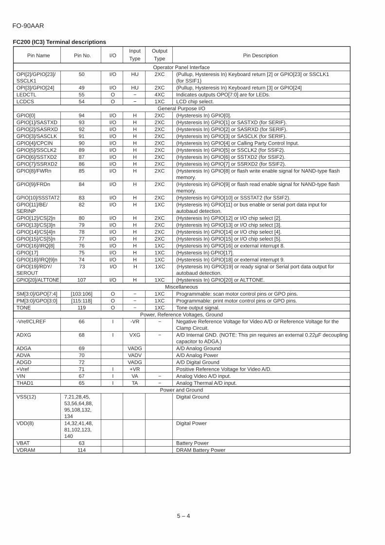
FO-90AAR
Operator Panel InterfaceOPI[2]/GPIO[23]/ 50 I/O HU 2XC (Pullup, Hysteresis In) Keyboard return [2] or GPIO[23] or SSCLK1SSCLK1 (for SSIF1)OPI[3]/GPIO[24] 49 I/O HU 2XC (Pullup, Hysteresis In) Keyboard return [3] or GPIO[24]LEDCTL 55 O − 4XC Indicates outputs OPO[7:0] are for LEDs.LCDCS 54 O − 1XC LCD chip select.
General Purpose I/OGPIO[0] 94 I/O H 2XC (Hysteresis In) GPIO[0].GPIO[1]/SASTXD 93 I/O H 2XC (Hysteresis In) GPIO[1] or SASTXD (for SERIF).GPIO[2]/SASRXD 92 I/O H 2XC (Hysteresis In) GPIO[2] or SASRXD (for SERIF).GPIO[3]/SASCLK 91 I/O H 2XC (Hysteresis In) GPIO[3] or SASCLK (for SERIF).GPIO[4]/CPCIN 90 I/O H 2XC (Hysteresis In) GPIO[4] or Calling Party Control Input.GPIO[5]/SSCLK2 89 I/O H 2XC (Hysteresis In) GPIO[5] or SSCLK2 (for SSIF2).GPIO[6]/SSTXD2 87 I/O H 2XC (Hysteresis In) GPIO[6] or SSTXD2 (for SSIF2).GPIO[7]/SSRXD2 86 I/O H 2XC (Hysteresis In) GPIO[7] or SSRXD2 (for SSIF2).GPIO[8]/FWRn 85 I/O H 2XC (Hysteresis In) GPIO[8] or flash write enable signal for NAND-type flash
memory.GPIO[9]/FRDn 84 I/O H 2XC (Hysteresis In) GPIO[9] or flash read enable signal for NAND-type flash
memory.GPIO[10]/SSSTAT2 83 I/O H 2XC (Hysteresis In) GPIO[10] or SSSTAT2 (for SSIF2).GPIO[11]/BE/ 82 I/O H 1XC (Hysteresis In) GPIO[11] or bus enable or serial port data input forSERINP autobaud detection.GPIO[12]/CS[2]n 80 I/O H 2XC (Hysteresis In) GPIO[12] or I/O chip select [2].GPIO[13]/CS[3]n 79 I/O H 2XC (Hysteresis In) GPIO[13] or I/O chip select [3].GPIO[14]/CS[4]n 78 I/O H 2XC (Hysteresis In) GPIO[14] or I/O chip select [4].GPIO[15]/CS[5]n 77 I/O H 2XC (Hysteresis In) GPIO[15] or I/O chip select [5].GPIO[16]/IRQ[8] 76 I/O H 1XC (Hysteresis In) GPIO[16] or external interrupt 8.GPIO[17] 75 I/O H 1XC (Hysteresis In) GPIO[17].GPIO[18]/IRQ[9]n 74 I/O H 1XC (Hysteresis In) GPIO[18] or external interrupt 9.GPIO[19]/RDY/ 73 I/O H 1XC (Hysteresis In) GPIO[19] or ready signal or Serial port data output forSEROUT autobaud detection.GPIO[20]/ALTTONE 107 I/O H 1XC (Hysteresis In) GPIO[20] or ALTTONE.
MiscellaneousSM[3:0]/GPO[7:4] [103:106] O − 1XC Programmable: scan motor control pins or GPO pins.PM[3:0]/GPO[3:0] [115:118] O − 1XC Programmable: print motor control pins or GPO pins.TONE 119 O − 1XC Tone output signal.
Power, Reference Voltages, Ground-Vref/CLREF 66 I -VR − Negative Reference Voltage for Video A/D or Reference Voltage for the
Clamp Circuit.ADXG 68 I VXG − A/D Internal GND. (NOTE: This pin requires an external 0.22µF decoupling
capacitor to ADGA.)ADGA 69 VADG A/D Analog GroundADVA 70 VADV A/D Analog PowerADGD 72 VADG A/D Digital Ground+Vref 71 I +VR Positive Reference Voltage for Video A/D.VIN 67 I VA − Analog Video A/D input.THAD1 65 I TA − Analog Thermal A/D input.
Power and GroundVSS(12) 7,21,28,45, Digital Ground
53,56,64,88,95,108,132,134
VDD(8) 14,32,41,48, Digital Power81,102,123,140
VBAT 63 Battery PowerVDRAM 114 DRAM Battery Power
FC200 (IC3) Terminal descriptions
Pin Name Pin No. I/OInput Output
Pin DescriptionType Type
5 – 4

FO-90AAR
(2) Panel control blockThe following controls are performed by the FC200.
• Operation panel key scanning
• Operation panel LCD display
(3) Mechanism/recording control block
• Recording control block diagram (1)
Fig. 4
5 – 5
OPERATORPANEL,
KEYPAD,LEDS & LCD
PANEL/LCD PWB
PRINTER DATACONTROI &SENSORS
THERMAL HEAD
OPO[7:0]*OPI[3:0]*LEDCTL*LCDCS*
TESTBATRSTNRESETN
STRB[3:0]STRBPOLTHADIPDATPCLKPLAT
TONE/ALTTONETSTCLKREGDMAWAITNSYNCPWRDWNN
PRINTER &SCANNER
MOTOR DRIVERS
MOTORPM[3:0]*
SM[3:0]*
RTCCRYSTAL
SCANNERCONTROLS &
SENSORS
STARTCLK2CLK1CLK1NVIDCTL[1:0]
XINXOUT
MIRONMCSN
SYSCLK
D[7:0]RDN
A[4:0]
WRN
MONOFAXFACSIMILE
MODEM
ANALOGSWITCH
LINEINTERFACE
SPEAKERMICROPHONE
CIRCUIT
TELEPHONELINE
RX
AT
XA SP
KR
MIC
RIN
SP
KR
LOS
PK
RH
I
SPKRRIN
TX
A2
TX
A1
TXOUTRXIN
XIA
GPIO
DRAM(OPTION)
SCANNERVIDEO
PREPROCESSING
SYNC PORTS (2)(SSIF)
VIN+VREF
–VREF
SSCLK[2:1]*SSTXD[2:1]*SSRXD[2:1]*SSSTAT[2:1]*
SYNC/ASYNCSERIALPORT
SASCLKSASTXD
SASRXD
GPIOGENERALPURPOSE I/O
CIS
DEBUGNVDDVDRAMVBATVSS
FLASH MEMORY
WRPROTNFRDN*FRWN*FCLE*FCS[0:2]
D[7:0]RDN
A[23:0]
WRNROMSCN
CS[5:0]N*
TXDATRMODE
RXDAT
TMODECLKINSLEEPN
GPIO
CAS[0,1]N,RASN,DWRN
NOTES:*ALTERNATIVE GPO,GPI OR GPIO LINES
SPEAKERPHONE ONLY
VOICE OR SPEAKERPHONE
EXTENDEDFACSIMILE
CONTROLLER
EX
TE
RN
AL B
US
D[7:0]

FO-90AAR
(4) Modem (FM209V) block
INTRODUCTIONThe CONEXANT FM209V MONOFAX modem is a synchronous 9600bits per second (bps) half-duplex modem with error detection and DTMFreception. It has low power consumption and requires a single +5V and+3.3V DC power supply. The modem is housed in a single VLSI devicepackage.The modem can operate over the public switched telephone network(PSTN) through line terminations provided by a data access arrange-ment (DAA).The FM209V is designed for use in Group 3 facsimile machines.The modem satisfies the requirements specified in CCITT recommen-dations V.29, V.27 ter, V.21 Channel 2 and T.4, and meets the binarysignaling requirements of T.30.The modem can operate at 9600, 7200, 4800, 2400, or 300 bps, andalso includes the V.27 ter short training sequence option.The modem can also perform HDLC framing according to T.30 at 9600,7200, 4800, 2400, or 300 bps.The modem features a programmable DTMF receiver and three pro-grammable tone detectors which operate concurrently with the V.21channel 2 receiver.The voice mode allows the host computer to efficiently transmit andreceive audio signals and messages.The modem is available in either a 128-pin plastic quad flat pack (TQFP).General purpose input/output (GPIO) pins are available for host assignment in the 128-pin TQFP.The modem’s small size, single voltage supply, and low power con-sumption allow the design of compact system enclosures for use in bothoffice and home environments.MONOFAX is a registered trademark of CONEXANT.
FEATURES
• Group 3 facsimile transmission/reception
- ITU-T V.29, V.27 ter, T.30, V.21 Channel 2, T.4
- ITU-T V.17 and V.27 ter short train
- HDLC framing at all speeds
- Receive dynamic range: 0 dBm to -43 dBm
- Automatic adaptive equalization
- Fixed and programmable digital compromise equalization
- DTMF detect and tone detect
- ITU-T V.21 Channel 2 FSK 7E Flag Detect
- Ring detector
- Programmable transmits level
- Programmable single/dual tone transmission
• V.23 and Type I Caller ID
- Full-duplex modes:
TX = 75 bps. RX = 1200 bps
TX = 1200 bps. RX = 75 bps
- Half-duplex mode:
TX = RX = 1200 bps
- Serial and parallel data modes
- Programmable parallel data mode
- 5, 6, 7 or 8 data bits
- 1 or 2 Stop bits
- Mark, Space, Even, or Odd Parity
- Break function
- Transmitter squelch
- Compromise equalizer
• Programmable interface memory interrupt
• Eight General Purpose Input (GPI) and eight General Purpose Out-put (GPO) pins for host assignment
• DTE interface: two alternate ports
- Selectable microprocessor bus (6500 or 8085)
- ITU-T V.24 (EIA/TIA-232-E compatible) interface
• TTL and CMOS compatible
• 3.3V/5V operation
• Power consumption
- Operating Mode: 200 mW (Basic), 275 mW (-V option). 300 mW(-VS option)
- Sleep Mode: 1 ma (Basic. -V option and -VS option)
• Packaging
- 128-pin TQFP (thin quad flat pack)
5 – 6
Fig. 5
USART(OPTIONAL)
HO
ST
PR
OC
ES
SO
R(D
TE
)
DECODER
CRYSTAL
DAA
SPEAKERDRIVER
(OPTIONAL)
EYEPATTERN
GENERATOR(OPTIONAL)
POWERSUPPLY
FM209VMONOFAX
MODEM
TXD
RXD
DCLK
RTS#
CTS#
RLSD#
READ#
WRITE#
DATA BUS
ADDR BUS
CS#
RESET#
IRQ1#
IRQ2#
XTLI
XTLO
EYECLK
EYESYNC
EYEXY
SPKRM
SPKRP
LINEIN
LINEOUT
RINGD
TALK
OFFHOOK
TELEPHONELINE
GN
D
+3.3V
+5V

FO-90AAR
5 – 7
FM209V (IC5) Hardware Interface Signals
Pin Signals – 128-Pin TQFP
Pin No. Signal Name I/O Type Pin Description
1 SR4IN/RESERVED MI Modem Interconnect2 SR3OUT/RESERVED MI Modem Interconnect3 EYESYNC OA Eye Pattern Circuit4 EYECLK OA Eye Pattern Circuit5 RXD OA DTE serial interface6 SR1IO MI Modem Interconnect7 NC — No Connection8 EYEXY OA Eye Pattern Circuit9 SR4OUT MI Modem Interconnect10 VDD1 PWR 3.3V Digital Supply for DSP11 RLSD# OB DTE Serial Interface12 DCLK OB DTE Serial Interface13 EN85# IA Host Parallel Interface14 GPI0 IA Host Parallel Interface15 RTS# IA DTE Serial Interface16 DGND1 GND DSP Digital Ground17 TXD IA DTE Serial Interface18 SA1CLK MI Modem Interconnect19 RS4 IB Host Parallel Interface20 RS3 IB Host Parallel Interface21 RS2 IB Host Parallel Interface22 RS1 IB Host Parallel Interface23 RS0 IB Host Parallel Interface24 YCLK I Modem Interconnect25 IACLK MI Modem Interconnect26 IA1CLK MI Modem Interconnect27 CTRLSIN S/NC MI Modem Interconnect28 RESERVED/NC MI Modem Interconnect29 SOUT S/NC MI Modem Interconnect30 SIN S/NC MI Modem Interconnect31 FSYNC S/NC MI Modem Interconnect32 IARESET S#/NC MI Modem Interconnect33 AGND1 GND IA Analog Ground34 LINEIN S/NC I Line Interface35 MICP S/NC I Microphone Input36 MICM S/NC I Microphone Input37 MICBIAS S/NC O Microphone Bias Output38 NC — No Connection39 NC — No Connection40 VREF S/NC MI Modem Interconnect41 VC S/NC MI Modem Interconnect42 VAA S/NC PWR 5V IA Analog power43 LINEOUT S/NC O Line Interface44 NC — No Connection45 AGND2 GND IA Analog Ground46 SPKRP S/NC O Speaker Interface Output47 SPKRM S/NC O Speaker Interface Output48 AVDD S/NC PWR 5V IA Digital power49 RESERVED/NC MI Modem Interconnect50 ICLK S/NC MI Modem Interconnect51 MCLK P MI Modem Interconnect52 CTRLSIN P MI Modem Interconnect53 RESERVED MI Modem Interconnect54 SOUT P MI Modem Interconnect55 SIN P MI Modem Interconnect56 FSYNC P MI Modem Interconnect57 IARESET P# MI Modem Interconnect58 AGND3 GND IA Analog Ground59 NC — No Connection60 LINEIN P I Line Interface61 MICP P I Microphone Input62 MICM P I Microphone Input63 MICBIAS P O Microphone Bias Output64 NC — No Connection65 NC NC No Connection66 VREF P MI Modem Interconnect67 VC P MI Modem Interconnect68 VAA P PWR 5V Analog Supply for IA69 LINEOUT P O Line Interface70 AGND4 GND IA Analog Ground71 SPKRP P O Speaker Interface Output

FO-90AAR
5 – 8
FM209V (IC5) Hardware Interface Signals
Pin Signals – 128-Pin TQFP
Pin No. Signal Name I/O Type Pin Description
72 SPKRM P O Speaker Interface Output73 AVDD P PWR 5V Digital power for IA74 NC — No Connection75 ICLK P MI Modem Interconnect76 MCLK S/NC MI Modem Interconnect77 VDD2 PWR 3.3V Digital Supply for DSP78 D7 IB/OC Host Parallel Interface79 D6 IB/OC Host Parallel Interface80 D5 IB/OC Host Parallel Interface81 D4 IB/OC Host Parallel Interface82 D3 IB/OC Host Parallel Interface83 D2 IB/OC Host Parallel Interface84 DGND2 GND DSP Digital Ground85 VDD3 PWR 3.3V Digital Supply for DSP86 D1 IB/OC Host Parallel Interface87 DGND3 GND DSP Digital Ground88 D0 IB/OC Host Parallel Interface89 CSBR# IB Host Parallel Interface90 WRITE# IB Host Parallel Interface91 CS# IB Host Parallel Interface92 READ# IB Host Parallel Interface93 GPI2 IA General purpose input94 GPI3 IA General purpose input95 GPI4 IA General purpose input96 GPI5 IA General purpose input97 GPI6 IA General purpose input98 GPI7 IA General purpose input99 GPO7 OC General purpose output
100 VDD4 PWR 3.3V DSP Digital Power101 GPO6 OC General purpose output102 GPO5 OC General purpose output103 RESERVED MI Modem Interconnect104 GPO4 OC General purpose output105 GPO3 OC General purpose output106 DGND4 GND DSP Digital Ground107 CTS# OB DTE Serial Interface108 IRQ1# OB Interrupt request109 GPO2 OC General purpose output110 GPO1 OC General purpose output111 GPO0 OC GPO0 (IA reset)112 VDD5 PWR 3.3V DSP Digital Power113 VGG PWR 5V DSP Digital114 DGND5 GND DSP Digital Ground115 RESET# IB External reset116 XTALI I Crystal in117 XTALO O Crystal out118 RESERVED MI Modem Interconnect119 XCLK OB X clock output120 GPI1 IA General purpose input121 IRQ2# OA Interrupt request122 SR3IN MI Modem Interconnect123 RESERVED MI Modem Interconnect124 RESERVED MI Modem Interconnect125 DGND6 GND DSP Digital Ground126 DVAA PWR 3.3V DSP analog power127 AGND5 GND DSP Analog Ground128 RESERVED MI Modem Interconnect
Notes:I/O types: MI = Modem interconnect.
IA, IB, = digital inputOA, OB, OC = digital outputI = analog inputO = analog output
P Signals: Primary IA S Signals: Secondary IAReserved = No external connection allowed.

FO-90AAR
[3] Circuit description of TEL/LIU PWB
(1) TEL/LIU block operational description
1) Block diagram
2) Circuit description
The TEL/LIU PWB is composed of the following 6 blocks.
1. Speech circuit section
2. Dial transmission section
3. Speaker amplifier section
4. Ringer circuit section
5. Externally connected TEL OFF HOOK detection circuit
6. CI detection circuit
Fig. 6
3) Block description
1. Speech circuit section
• The receiver volume is an electronic volume type, this model isswitched in 2 steps.
2. Dial transmission section
• D.P. transmission: The CML relay and PC1 are turned on and offfor control in the DP calling system. (Refer to the attached sheet.)
• DTMF transmission: It is formed in the modem, and is output.
3. Speaker amplifier section
• Ringer volume : It is controlled by the combination of the attenuatorvalue of the LINE DRIVER in the modem and theringer sending level sent from the modem.
• Speaker volume: It is controlled by the attenuator value of the LINEDRIVER in the modem.
4. Ringer circuit section
• The ringer sound is formed in the tone of modem when CI signal isdetected. The amplifier circuit drives the speaker of the main body.
5 – 9
H
~~
+–
HSL
L
HDPON DPMUTE
DPON
IACR1
IACR2
IACR3
BIT7 BIT6 BIT5 BIT4 BIT3 BIT2 BIT1 BIT0DACGAIN
MIC GAIN L/O E SPKR E ADCGAIN
L/I E MIC E
TXRXLOOP
LINEOUTATTENUATION
RXTXLOOP MICBIASSEL
LINE SEL
CONTROL PWBTEL/LIU PWB
RX
TX
HANDSET
SPDRIVER
CUTIHSCI
CSWIPESNSFRSNSORGSNSPSNS
BZOUTCMLSPMUTE
VREFCONTMDMRST
FAXENGINEFC200
ADC
DACSIN
DAC GAIN0,6dB
SOUT
ADC GAIN0,–4dB
MIC INLPF
LINE INLPF
SP OUTENABLE
0,20,25,30dB
LINEDRIVER
LINEOUTENABLE
MUTE,0,–6,–12dB
RHS
RANK
DRSNS
TXMUTE
TELMUTE
IA-RESET
SPMUTE
SPEAKER
TELMUTE
TELIN
CI
M
BC
CMLL1
L2
FAX MODEM FM209V
TELOUT
RXIN
TXOUT SPKRP-P
MICP
LINEIN
LINEOUT
RTLOOP(0:1)(1:0)(0:0)(1:1)
MIC ENABLE
MICENABLE1
0
LINE INENABLE1
0
(0:0)(1:1)(1:0)
LNINSEL
MICGAIN
VOL_C
RXCONT
W-TONE
VOL_A
VOL_B
RCVOLLEDONVTHON
TXMUTE
4051
VOL_CVOL_BVOL_A

FO-90AAR
5. Externally connected TEL OFF HOOK detection circuit section
• The circuit current detection is turned on together with OFF HOOKof main body or OFF HOOK of externally connected TEL. ON ofCML OFF (HS=L) is judged as OFF HOOK of externally connectedTEL.
6. CI detection circuit
• CI is detected by the photocoupler which is integrated in series inthe primary side TEL circuit well proven in the existing unit.
5 – 10
Signal Name Description
CML Line connecting relay(The circuit is located H: Line makein the TEL/LIU PWB.) L: Line break
SP MUTE Speaker tone mute control signal(The circuit is located H: Muting (Power down mode)
in the TEL/LIU PWB.) L: Muting cancel (Normal operation)
Handset reception mute control signalTEL MUTE H: Muting
L: Muting cancel
DPON Connecting DC circuit and DP generating(The circuit is located H: Line connect / Make in the TEL/LIU PWB.) L: Line disconnect / Break
DPMUTE Adjust the resistance during make ratio
(The circuit is located H: Muting in the TEL/LIU PWB.) L: Muting cancel
TXMUTE Tx route mute circuit(The circuit is located H: Mutingin the control PWB.) L: Muting cancel
4) Signal selection
The following signals are used to control the transmission line of TEL/FAX signal. For details, refer to the signal selector matrix table.
[Control signals from output port]
VOL A VOL B VOL C ON-HOOK ICM/OGM ICM/OGM
OUTPUT VALUE (GP02) (GP03) (GP04) Receiving MONITOR PLAY RINGER BUZZER DTMF/DP
X 0 1K 0 0 0 — — HIGH HIGH — —
X 1 10K 1 0 0 HIGH HIGH MIDDLE1 — — —
X 2 39K 0 1 0 MID 1 MID 1 MIDDLE2 — — —
X 3 100K 1 1 0 MID 2 MID 2 MIDDLE3 — — —
X 4 200K 0 0 1 MID 3 MID 3 LOW MIDDLE — —
X 5 300K 1 0 1 — — — — — FIXED
X 6 470K 0 1 1 LOW LOW — — FIXED —
X 7 750K 1 1 1 — — — LOW — —
VOLUME SETTING

FO-90AAR
(Example: TEL speaking)
NO Signal Name (CNLIUA)
1 TELOUT
2 TELIN
3 TELMUTE
4 CI
5 HS
6 RHS
Fig. 7
Signal Name Function
RHSH:The handset is in the on-hook state.
L: The handset is in the off-hook state.
CI Incoming call (CI) detection signal
[Signals for status recognition according to input signals]
Signal Name Function
TEL IN Receiving signal from line or modem
TEL OUT Transfer signal to line
SPOUT Speaker output signal
TXOUTTransmission (DTMF) analog signal output
from modem
RXINReception (DTMF, others) analog signal input
into modem
[Other signals]
5 – 11
NO Signal Name (CNLIUA)
7 RXIN
8 TXOUT
9 CML
10 +5V11 DG
12 +24V
TX/RX SIGNAL
OGM/ICM/MEMO/PLAYBACK SIGNAL
OGM/MEMO/RECORD SIGNAL
H
~~
+–
HSL
L
HDPON DPMUTE
DPON
IACR1
IACR2
IACR3
BIT7 BIT6 BIT5 BIT4 BIT3 BIT2 BIT1 BIT0DACGAIN
MIC GAIN L/O E SPKR E ADCGAIN
L/I E MIC E
TXRXLOOP
LINEOUTATTENUATION
RXTXLOOP MICBIASSEL
LINE SEL
CONTROL PWBTEL/LIU PWB
RX
TX
HANDSET
SPDRIVER
CUTIHSCI
CSWIPESNSFRSNSORGSNSPSNS
BZOUTCMLSPMUTE
VREFCONTMDMRST
FAXENGINEFC200
ADC
DACSIN
DAC GAIN0,6dB
SOUT
ADC GAIN0,–4dB
MIC INLPF
LINE INLPF
SP OUTENABLE
0,20,25,30dB
LINEDRIVER
LINEOUTENABLE
MUTE,0,–6,–12dB
RHS
RANK
DRSNS
TXMUTE
TELMUTE
IA-RESET
SPMUTE
SPEAKER
TELMUTE
TELIN
CI
M
BC
CMLL1
L2
FAX MODEM FM209V
TELOUT
RXIN
TXOUT SPKRP-P
MICP
LINEIN
LINEOUT
RTLOOP(0:1)(1:0)(0:0)(1:1)
MIC ENABLE
MICENABLE
1
0
LINE INENABLE
1
0
(0:0)(1:1)(1:0)
LNINSEL
MICGAIN
VOL_C
RXCONT
W-TONE
VOL_A
VOL_B
RCVOLLEDONVTHON
TXMUTE
4051
VOL_CVOL_BVOL_A
NO Signal Name (CNLIUB)
1 N. C.
2 N. C.
NO Signal Name (CNLIUB)
3 DPON
4 DPMUTE

FO-90AAR
[4] Circuit description of power supply PWB
1. Block diagram
2-1. Noise filter circuitThe input noise filter section is composed of L1, C1, C15 and C21 whichreduces normal mode noise from the AC line and common mode noiseto the AC line.
2-2. Rectifying/smoothing circuitThe AC input voltage is rectified by diode D1, 2, 3, 4 and smoothed bycapacitor C2 to supply DC voltage to the switching circuit section.
Power thermistor TH1 suppresses inrush current at power switch-on.
2-3. Switching circuitThis circuit includes MOS FET Q1 and the gate drive circuit, and com-ponents around Q1.
In this circuit, the DC voltage supplied from the rectifying/smoothing sec-tion is converted into high frequency pulses by ON/OFF repetition ofQ1.
[5] Circuit description of CIS unit
1. CIS (Contact Image Sensor)Cis is an image sensor which puts the original paper in close contactwith the full-size sensor for scanning, being a monochromatic typewith the pixel number of 1,728 dots and the main scanning density of8 dots/mm.
It is composed of sensor, rod lens, LED light source, light-conductiveplate, control circuit and so on, and the reading line and focus arepreviously adjusted as the unit.Due to the full-size sensor, the focus distance is so short that the setis changed from the light weight type to the compact type.
Fig. 9
Fig. 8
5ms
1.984µs0V
2V(TYP)(White original paper)
Approx.5VøT
CISCLK
VO
5 – 12
2. WaveformsThe following clock is supplied from FC200 of the control board, andVO is output.
2-4. Control circuitThis circuit controls output voltage of 24V by adjusting ON period of Q1,looking at signal from photo-coupler PC1.In this operation IC1 takes charge of important part.The over current protection is performed by bringing Q1 to OFF statethrough detection of voltage of T1 subwiding.The over voltage protection is performed by operating the over currentprotection circuit through detection of zener diode ZD4 and short-circuitingof load.
2-5. +5V circuitDC voltage supplied by rectifying the output of transformer T1 with diodeD8 is stabilized by 3-terminal regulator IC1.
NoiseFilter
Circuit
RectifyingSmoothing
CircuitSwitching
Circuit(RCC system)
RegulatorCircuit
+5V
+24V
AC IN
Photo Coupler
F11.6A/250V
F21.6A/250V
ControlCircuit
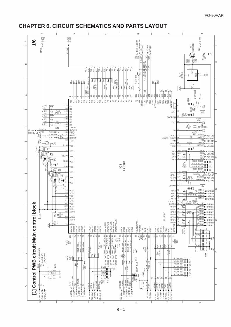
FO-90AAR
CHAPTER 6. CIRCUIT SCHEMATICS AND PARTS LAYOUT[1
] Con
trol
PW
B c
ircui
t Mai
n co
ntro
l blo
ck1/
6
6 – 1
126 4 35
BD
EF
GI
HC
A
126 4 35
BD
EF
GI
HC
A
107 73 74 75 76 77 79 80 82 83 84 85 86 87 89 90 91 92 93 94 96 97 100 99 98 101 33 34 35 36 29 30 31 37
3839404243444647545549505152
114
115116117118
103104105106
11965676671
59
60
62
63
61
78
70
7269
681401231028148
3214
21
28
45
53,56
64,88
95,108
132
7,134
58129131135133130136137138139
+5V C
155
0.1
C15
31
DG
+5V
141142143144
(3-2A)(3-3B)
SYSCLKMIRQ
R15
010
KC
118
1000
P
DG
R107 33K
R108 33KR100 33K
D7D6D5D4D3D2D1D0
RA3270 x 4
RA4270 x 4
(2-6
A)
(3-4
B)
M
NL
41
DG
DG
DG
DG
DG
DG
DG
DG
C13
3C
159
C15
8C
156
C15
1C
132
C11
4C
117
1 2 3 4 5 6 8 9 11 12 13 15 16 17 18 19 20 22 23 24 25 26 27 128
127
120
122
57 121
126
124
125
113
112
111
109
110
10
A B C D E F
A16
A15
A14
A13
A12
A11
A10 A9
A8
A7
A6
A5
A4
A3
A2
A1
A0
RA
627
0 x
4
RA
1327
0 x
4
I KJ
H
(2-6
A)
(3-4
B)
(2-4
D)(
3-3B
)(2
-4A
)
(2-4
D)
(3-3
B)
R12
3 2
00R
125
270
VBT
C17
21
R16
81M
C17
30.
1
DG
BA
TR
ST
DG
+5V
VC
C
GN
DOU
TC
171
1
MC
SC
E1
RO
MC
SW
RR
D
(2-2
D)
CE
2
IC7
XC
61
DG
DGC175
2200P
R16
710
M
C17722P
C17618P
X232.768kHz
(5-2D)+VREF
(5-2D)–VREF
(5-6D)VIN
(5-1I)THADI
(6-1G)BZOUT
(5-5F)TPA
(5-5F)TPB
(5-5F)TPA
(5-5F)TPB
DG
C1781
DG
DG
DGDGDGDGC110 1000P
C109 1000PC108 1000PC107 1000P
RA
127
0 x
4
(5-5F)VTHON
(5-5F)LEDON
(3-2B)MDMRST
(6-3C)(6-5E)RCVOL
DG
C11
30.
1
+5V
CNPN-16CNPN-15CNPN-14CNPN-13
CNPN-4CNPN-5CNPN-6CNPN-7CNPN-8CNPN-3CNPN-9CNPN10CNPN-11
KEN1AKEN2AKEN3AKEN4A
ESEN0SEN1SEN2SEN3SEN4SEN5SEN6SEN7
L108HM601
R169120
RA14470 x 4
RA15470 x 4
A23
A22
A21
A20
A19
A18
A17
A16
A15
A14
A13
A12
A11
A10 A9
A8
A7
A6
A5
A4
A3
A2
A1
A0
RD
WR
RO
MC
SC
S1
CS
0M
CS
SY
NC
RE
GD
MA
WA
ITR
AS
CA
S0
CA
S1
DW
RW
RP
RO
T
VBAT
CN
TH
-13
LAT
CH
CN
TH
-15
DA
TA
CN
TH
-14
PC
LKC
NT
H-3
ST
RB
1C
NT
H-4
ST
RB
2C
NT
H-1
1S
TR
B3
CN
TH
-12
ST
RB
4
RA
1147
0 x
4
RA
1227
0 x
4
DGC180 22P
DGC181 22P
DGC139 22P
DGC140 22P
DGC194 22P
DGC193 22P
DGC179 22P
CN
CIS
-4C
NC
IS-5
CIS
CLK
D[7
-0]
A[1
7-0]
R11
6 1
50R
120
470
L102
HM
601
(4-2
D)
PS
NS
(4-5
D)
OR
GS
NS
I(4
-5D
)F
RS
NS
I(4
-3D
)P
ES
NS
CN
LIU
B-4
DP
MU
TE C
221
N.M
.
R14
847
0R
A5
470
x 4
R12
4 3
3KR
122
33K
R11
8 3
3KR
119
33K
CN
LIU
B-5
E-R
LY
CN
LIU
B-3
DP
ON
CN
PW
-8P
SA
VE
CN
LIU
B-1
RLY
CN
T
(4-6
D)
CS
WI
C220C222C217C218
N.M
.
RA
1047
0 x
4
R14
347
0
R14
733
K
CI
HS
(6-2
I)S
PM
UT
EC
ML
(5-2
A)
VR
EF
CO
NT
(4-4
D)
CU
TI
GP
IO20
GP
IO19
GP
IO18
GP
IO17
GP
IO16
GP
IO15
GP
IO14
GP
IO13
GP
IO12
GP
IO11
GP
IO10
GP
IO9/
FR
DG
PIO
8/F
WR
GP
IO7/
FC
LEG
PIO
6/F
ALE
GP
IO5/
FR
EA
DY
GP
IO4
GP
IO3
GP
IO2
GP
IO1
GP
IO0
VID
CT
L0/F
CS
1V
IDC
TL1
CLK
1C
LK1
CLK
2S
TA
RT
ST
RB
3S
TR
B2
ST
RB
1S
TR
B0
PC
LKP
DA
TP
LAT
ST
RB
PO
L
D0D1D2D3D4D5D6D7TSTCLKSYSCLKMIRQRESETDEBUGTEST
VSS
VSS
VSS
VSS
VSS
VSS
VSS
VSS
VDDVDDVDDVDDVDDVDDVDDVDDADXG
ADGAADGD
ADVA
BA
TR
ST
PWRDWN
XOUT
XIN
+VREF–VREF / CLREF
VINTHADITONE
SM0SM1SM2SM3
GPO0GPO1GPO2GPO3
VDRAM
OPI0OPI1OPI2OPI3
LEDCTLLCDCS
OPO0OPO1OPO2OPO3OPO4OPO5OPO6
38 :
OP
O7
2
1
3
R16
610
K
RA2470 x 4
R15
210
K
RA
947
0 x
4
R10
447
0
R11
747
0
R10
533
K
R15
1 33
KR
149
33K
R12
1 33
K
(2-4
A)(
3-3B
)D
G
DG
IC3
FC
200
A17
R12
727
0
RA
827
0 x
4
RA
727
0 x
4
C13
5C
136
N.M
.
DG
DG
DG
DG
R16
410
K
Q3
2SC
2412
K
RA
1647
0 x
4
CA2
CA1
DG
DG
N.M
.
PH
IT
C14
2C
143
N.M
.
FC
S
R21
327
0
FR
EA
DY
FA
LEF
CLE
FW
RF
RD
R21
933
KR
214
270R21
5 27
0R
216
270
R21
7 27
0R
218
270
N.M
.
C13
41
C16
0 1
C15
7 1
C15
4 1
C15
2 1
C13
1 1
C11
5 1
C11
6 1
R12
6 2
70
R16
310
K
(2-1
D)
(2-2
D)
(2-3
D)
(2-3
D)
(2-3
D)
(2-2
D)
(1-6
B)
(1-6
B)
(1-6
B)
CM
LH
S CI
(1-5
A)(
6-4E
)(1
-5A
)(1
-5A
)
C205C200C197
N.M
.
CN
LIU
A-9
CN
LIU
A-5
CN
LIU
A-4
CM
LH
SC
I

FO-90AAR
Mem
ory
bloc
k2/
6
126 4 35
BD
EF
GI
HC
A
126 4 35
BD
EF
GI
HC
A
21 2029
1928
18 1725
1523
1426
1327
31 32 110 11
1622 24
1IO
819
26IO
718
A14
2
A14
IO6
17A
13
23
A13
IO5
16A
12
21
A12
IO4
15A
11
24
A11
IO3
13A
10
25
A10
IO2
12A
9
3
A9
IO1
11A
8
4
A8
A7
5
A7
A6
6
A6
A5
7
A5
VD
D28
A4
8
A4
VS
S14
A3
9
A3
A2
10
A2
A1
A0
27
A0
22C
S2/
OE
A[1
7~0]
(1-5
I)
D[7
~0]
(1-6
I)
(1-3
H)
RD
(1-3
H)
+5V
DG
C21
60.
1
D7
D6
D5
D4
D3
D2
D1
D0
IC10
27C
020
3A
15D
7A
14D
6A
13D
5A
12D
44
A11
D3
A10
D2
A9
D1
A8
D0
A7
5
A6
6
A5
PG
M7
A4
VC
C8
A3
VP
P9
A2
A1
A0
GN
DC
EO
G
IC6
W24
258S
-70L
E
A1
WE
D7
D6
D5
D4
D3
D2
D1
D0
VB
T
DG
C16
10.
1
WR
(1-3
H)
VB
T
R12
822
K
RO
MC
S
2A
16A
15A
14A
13A
12A
11A
10A
9A
8A
7A
6A
5A
4A
3A
2A
1A
0
A16
1220
CS
1C
E1
(1-3
H)
30A
17A
17
L110 0
2I/O
727
I/O6
26F
CLE
3
CLE
I/O5
25
I/O4
24F
ALE
4
ALE
I/O3
21
I/O2
20F
WR
5
WE
I/O1
19
I/O0
18C
E2
WP
41V
CC
44
FR
EA
DY
42
R/B
GN
D40
FR
D
43
RE
FC
SC
E
IC4
KM
29W
040
D7
D6
D5
D4
D3
D2
D1
D0
+5V
DG
C11
90.
1
23 1 22
VC
C
VS
SV
SS
R10
9R
133
R13
2R
131
R13
0R
129
R15
4R
153
(1-4
B)
(1-4
B)
(1-4
B)
(1-1
I)
(1-4
B)
(1-4
B)
(1-3
B)
100
x 8
6 – 2

FO-90AAR
Mod
em b
lock
3/6
126 4 35
BD
EF
GI
HC
A
BD
EF
GI
HC
A
126 4 35
D7
A0
C13
00.
01
R10
127
0
D6
D5
D4
D3
D2
D1
D0
A1
A2
A3
A4
19 20 21 22 23
RS
4R
S3
RS
2R
S1
RS
0
78D
779
D6
80D
581
D4
82D
383
D2
86D
188
D0
91C
S92
RE
AD
90W
RIT
E10
8IR
Q1
115
RE
SE
T13
EN
85
DG
D[7
~0]
RD
WR
(1-3
H)
(1-3
H)
(1-3
H)
R18
7
MIR
Q(1
-6F
)
A[4
~0]
MD
MR
ST
(1-1
D)
MC
S MA
G
121
IRQ
2
N.M
.
15 107 17 12 5
RT
SC
TS
TX
DD
CLK
RX
D11
RLS
D
R14
110
K
RE
SE
RV
ED
/CS
BR
DG
DG
89 119 24
R11
327
0
+5V
SY
SC
LK(1
-6F
)
6217
35
8
XC
LKY
CLK
CLRD
CLK
PR
E
C2
QL1
00H
M60
1
R10
647
0
L103
HM
601
C11
11
IC2
WT
74
L101
HM
601
99101102104105109110111
R13
447
0
R135470
R13
810
K
TXMUTETELMUTE
5732
348
DG
DG
DG
DG
DG
DG
R10
30
C10
610
PC
105
10P
R10
210
0
65227561831512576955302675505412229
116
117
DG
2874140433447463736351,2,
53,1
03,1
18,1
23,1
24,1
2838
,39,
44,4
9,59
,64,
65,7
4
MA
G
6766
C16
60.
1
C16
70.
1
C4
10/5
0
C1
10/5
0 MA
G
69(6
-3C
)S
PO
UT
60(6
-6E
)T
ELO
UT
I
(6-2
D)
SIG
TX
(6-4
E)
SIG
RX
7271636261C
168
0.1
R16
02.
2K
R16
21K
MA
G
CNDR-1
C14
722
00P
R13
747
0
+5V
R11
010
0K
989796959493
12014
CNTH-6 RANKCNLIUA-6 RHS
R11
547
0
R13
947
0
+3.3V
L106
HM
601
DG
107785
100112
73
168487
106114
125
113
12648
3345
+5V
L104
HM
601
C12
70.
1
+3.3V
R16
13
C3
47/2
5
C16
91
5870
127
68
C14
61
+5V
L105
HM
601
MA
GM
AG
DG
MA
G
MIC
P-P
MIC
M-P
MIC
BIA
S-P
SP
KR
P-P
SP
KR
M-P
LIN
EIN
-P
LIN
EO
UT
-PV
RE
F-P
VC
-P
RE
SE
RV
ED
N.C
./MIC
M-S
N.C
./SP
KR
P-S
N.C
./LIN
EIN
-S
N.C
./VR
EF
-S
N.C
./MIC
P-S
N.C
./MIC
BIA
S-S
N.C
./SP
KR
M-S
N.C
./LIN
EO
UT
-S
N.C
./VC
-S
N.C
.N
.C.
N.C
.
XT
LO
XTLI
N.C./SOUT-SSR3IN
SOUT-PN.C./ICLK-S
ICLK-PIA1CLK
N.C./SIN-SSIN-P
SR4OUTN.C./MCLK-S
IACLKMCLK-P
N.C./FSYNC-SSA1CLK
FSYNC-PN.C./CTRLSIN-S
CTRLSIN-PSR1IO
EYEXYEYECLK
EYESYNC
N.C./IARESET-SIARESET-P
GPO0W-TONE/GPO1
VOL-C/GPO2VOL-B/GPO3VOL-A/GPO4
MONITOR/GPO5GPO6GPO7GPI7
GPI6GPI5GPI4GPI3GPI2GPI1GPI0
VDD1(+3.3VDD)VDD2(+3.3VDD)VDD3(+3.3VDD)VDD4(+3.3VDD)VDD5(+3.3VDD)AVDD-P(+3.3VIAD)
DGND1DGND2DGND3DGND4DGND5DGND6
VGG(+5VDD)
DVAA(+3.3VDA)N.C./AVDD-S(+3.3VIAD)
AGND1AGND2AGND3AGND4AGND5
VAA-P(+5VIAA)
VA
A-S
(+5V
IAA
)
42
R14
233
KR
114
33K
R14
00
DG
X1
32.2
56M
Hz
DG
CNLIUA-3
CNLIUB-2
(1-6
I)
(1-6
I)
IC4
FM
209V
C19
810
00P
C199
(6-1C)
W-TONEVOL_CVOL_BVOL_A
C219
TXMUTE
N.M
.
R13
6R
158
R11
2
R22
2
N.M
.
R22
033
KC
124
N.M
.
DG
4
C11
20.
1
C22
7
DG
N.M
.
R12
3 DG
N.M
.
R11
110
0K
C13
70.
1
DG
C12
91
C150 1C149 1
C125 1C126 1
C14
81
C14
50.
1C
170
0.1
C12
81
(6-1C)(6-2G)(6-2G)(6-2G)
6 – 3

FO-90AAR
Sen
sor/
Res
et/P
ower
sup
ply
bloc
k4/
6
6 – 4
126 4 35
BD
EF
GI
HC
A
BD
EF
GI
HC
A
126 4 35
CN
CS
W-1
CN
CS
W-2
CS
W
DG
(1-4
A)
CN
FR
S-1
CN
FR
S-2
FR
SN
S
DG
(1-3
A)
CN
PN
-12
OR
GS
NS
(1-3
A)
(1-3
A)
+24
V
C12
022
00P
DG
CS
WI
C12
222
00P
DG
FR
SN
SI
C18
322
00P
DG
OR
GS
NS
I
PE
SN
SR
191
DG
R17
0
(1-3
A)
PS
NS
13
24
DG DG
DG
13
24
PE
SN
S
PS
NS
PI2
SG
206
PI1
SG
206
CN
CU
T-1
CN
CU
T-2
CU
T
DG
(1-5
A)
C12
122
00P
DG
CU
TI
DG
+5V
R21
15.
6K
BA
T1
CR
2032
D6
HR
W02
02
VB
T
<V
BT
>
+3.
3V2
3
1D2
1SS
355
RE
G10
0X
C62
C19
20.
1
DG
DG
+5V
+24
V
+24
VA
C10
22/5
0
C22
30.
1
R20
6R
207
FG
N.M
.
C11
47/2
5C
224
0.1
+5V
DG
DG
+24
V+
24V
MG
MG
+5V DG
DG
+24
V
CN
LIU
A-1
0
CN
LIU
A-1
1
CN
PN
-1
CN
LIU
A-1
2
CN
PW
-2
CN
PW
-1C
NP
W-7
CN
PW
-5C
NP
W-6
CN
PW
-3C
NP
W-4
R21
2
C8
DG
MG
DG
N.M
.N
.M.
CN
CU
T-3
DG
IR
Q
R155
C229
C228
N.M
.
+5V
CN
PN
-2
DG
C20
610
00P
+5V
C19
610
00P
N.M
.
R2
2.2K
(1/2
W)
R1
2.2K
(1/2
W)
N.M
.

FO-90AAR
Vid
eo p
roce
ssin
g/M
otor
driv
e / T
herm
al b
lock
5/6
6 – 5
126 4 35
BD
EF
GI
HC
A
BD
EF
GI
HC
A
126 4 35
R15
75.
1K
+5V
O
DG
Q2
2SA
1037
CN
CIS
-1
<V
O>
VO
(1-1
F)
<V
IN>
VIN
C16
410
00P
+5V
OC
NC
IS-3
CN
CIS
-2
<D
G>
DG
+5V
+24
VC
NC
IS-7
MG
+24
V
C16
51
C14
10.
1
GLE
DC
NC
IS-6
DG
C14
40.
1
LED
ON R
165
5.1K
DG
Q4
2SA
1037
(1-5
A)
VR
EF
CO
NT
(1-1
F)
VR
EF
+
+5V
R14
620
K
(1-1
F)
VR
EF
–R
145
30K
DG
R14
443
K
9 16 15 14 13 12 11 10
1 2 3 4 5 6 7 8
TP
AT
PB
TP
AT
PB
VT
HO
NLE
DO
N
(1-1
E)
(1-1
E)
(1-1
E)
(1-1
E)
(1-1
E)
(1-1
D)
+24
V
FU
100
KA
B24
02
D1
100(
1W)
VM
TV
MT
TP
BD
TP
AD
TP
BD
TP
AD
VT
HO
NLE
DO
N
CN
MT
-5C
NM
T-6
CN
MT
-1C
NM
T-2
CN
MT
-3C
NM
T-4
(5-3
E)
(5-4
B)
IC1
ULN
2003
A
1B 2B 3B 4B 5B 6B 7B E
CO
M 1C 2C 3C 4C 5C 6C 7C
VT
HO
N(5
-5I)
+24
V
D3
1SS
355
RY
1D
Q1U
24V
DC
+24
VV
TH
CN
TH
-1V
TH
CN
TH
-2V
TH
CN
TH
-16
MG
CN
TH
-7M
GC
NT
H-8
MG
CN
TH
-9
R15
622
K
MG
+5V
CN
TH
-10
+5V
(1-1
E)
CN
TH
-5T
HI
TH
AD
I
C16
31
R20
920
K
R20
847
0K
MG
C9
10/5
0
MG
MG
C2
R15
90
(5-5
I)
DG
C22
6
N.M
.
DG
+5V
O
DG
C17
4N
.M.
C16
2
MG
C13
8
MG
C10
0 C101C102C104C103
N.M
.
MGDGDGDGDGN
.M.
N.M
.
N.M
.
N.M
.

FO-90AAR
Ana
log
sign
al b
lock
6/6
6 – 6
126 4 35
BD
EF
GI
HC
A
BD
EF
GI
HC
A
126 4 35
– ++
5V
+5V
A
+5V
– +
+5V
– ++
5VA
+5V
+24
VA
+5V
TE
LOU
TC
NLI
UA
-1
C19
50
R19
30
C20
3N
.M.
R19
4
N.M
.
12 3
IC11
R19
20
R19
5N
.M.
C18
2
R17
60
C18
4H
M60
1
D4
1SS
355
TE
LOU
TI
(3-4
H)
(3-3
H)
SP
OU
T6
45
2 3
17
8
+5V
R19
810
0K
C20
922
0P
R21
022
0K
C7
47/2
5
SP
+
DG
SP
–
CN
SP
-1
CN
SP
-2
(1-5
A)
SP
MU
TE
C21
01
DG
DG
(1-1
E)
BZ
OU
T
R20
410
KC
190
4700
P
R20
520
K
DG
DG
DG
R20
110
0KC
215
0.01
R20
33K
C21
30
IC12
NJM
2113
N.M
.
L111 0
C5
DG
DG
CN
MIC
-1
CN
MIC
-2
CN
MIC
-3
DG
DG
DG
R18
1
R18
0R
182
C6
C22
5N
.M.
C18
61
R17
8N
.M.
Q1
RC
VO
L(1
-1D
)
DG
RX
INC
NLI
UA
-7
C20
70
R17
30
C20
8N
.M.
R17
5
N.M
.
76 5
IC11
R19
70
R17
1
R17
70
C18
5H
M60
1
D5
1SS
355
SIG
RX
(3-4
H)
DG
CN
LIU
A-2
DG
C18
91
R17
9N
.M.
Q6
CM
L(1
-5A
)
DG
TE
LIN
C20
40.
1
R19
647
K
C20
20
R17
2
R17
4N
.M.
DG48C
201 D
G
DG
Q5
RC
VO
L(1
-1D
)
IC9
HC
F40
5113 14 15 12 1 5 2 4
+5V
3 16 6 7 8
C19
11
DG
(3-1
D)
VO
L_C
(3-1
D)
VO
L_B
(3-1
D)
VO
L_A
R18
475
0K
R18
347
0K
R18
530
0K
R20
220
0K
R18
610
0K
R18
839
K
R18
910
K
R19
01K
R19
915
KC
214
0.1
CN
LIU
A-8
TX
OU
TC
211
0.1
C21
21
L107
HM
601
SIG
TX
W-T
ON
E
C18
8
C18
7R
221
5 4
1 2 3
IN/O
UT
OU
T/IN
VS
S
VD
D
CO
NTIC
8
N.M
.T
XM
UT
E
DG
DG
Q7
RN
C14
02
X0
X1
X2
X3
X4
X5
X6
X7
X
VD
D
VS
SV
SS
VS
S A B C
11 10 9
(3-1
C)
(3-1
D)
(3-4
H)
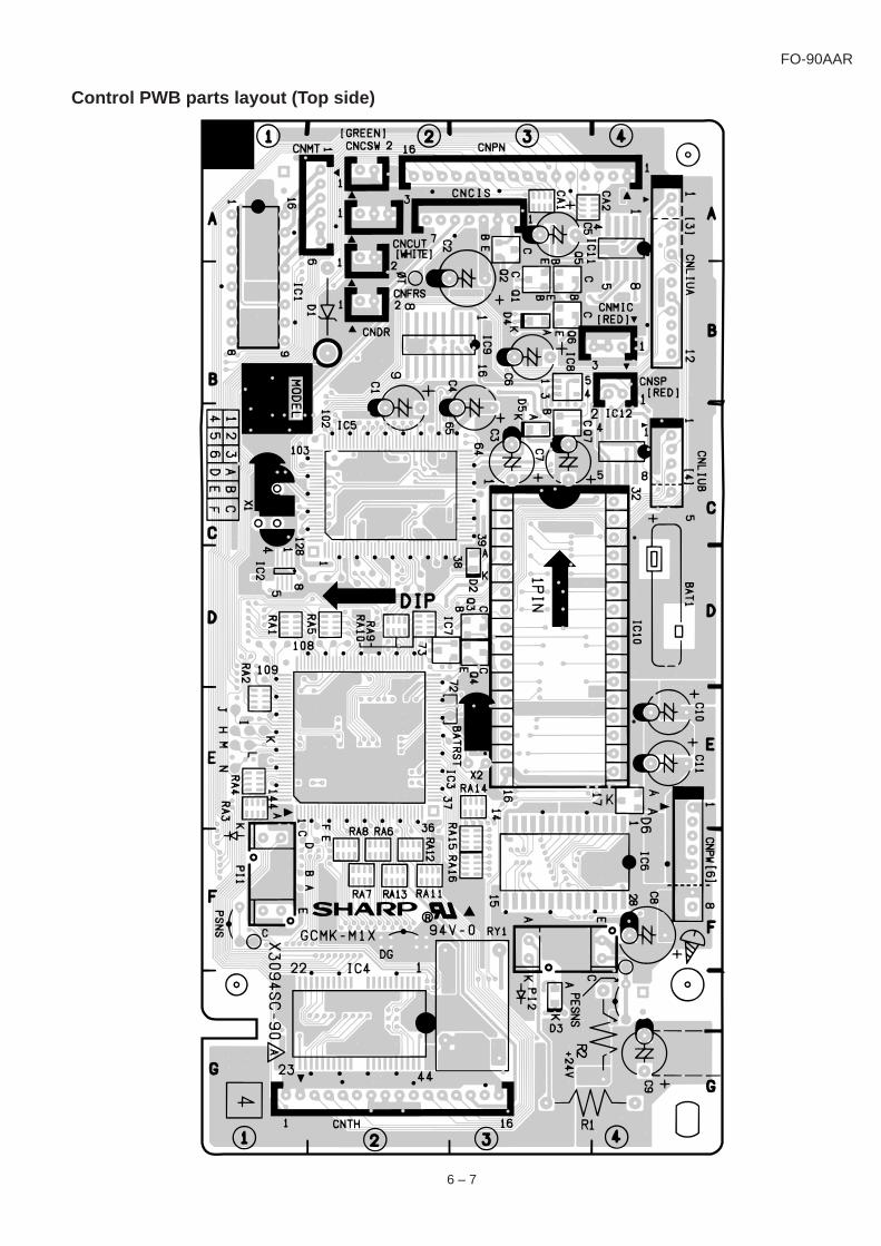
FO-90AAR
Control PWB parts layout (Top side)
6 – 7
FO-90AAR
Control PWB parts layout (Bottom side)
6 – 8

FO-90AAR
6 – 9
[2] T
EL/
LIU
PW
B c
ircui
t1/
2
126 4 35
BD
EF
GI
HC
A
BD
EF
GI
HC
A
126 4 35
– ++
5VA
+5V
A
– +
+5V
A
+24
VA
+5V
VR
EF
+5V
– +V
RE
F
+5V
– +
VR
EF
L3B
TLJ
-2
CN
LNJ-
2
L4 JP13
JP10
JP8
CN
LNJ-
3JP
9
JP6
CN
LNJ-
4
VA
2R
A-5
01P
-V6
VA
1R
A-5
01P
-V6
AR
G
CN
LNJ-
5
JP11
TLJ
-1
JP12
L1
JP1
JP15
C10
2
L54.
7mH
C10
1
L2
N.M
.
N.M
.
L3A N.M
.
JP3 N.M
.
CM B
CM
L2
C3
0.56
R10
143
K R3
22K
(1/2
W)
D11SS133
ZD
4M
TZ
J20B
PC
5T
LP52
1
R1
C1
R10
30
C2
1.5
N.M
.
2 1
4 3
T1
I216
4
C10
30.
022
C11
6
N.M
.
~ ~+ –
RE
C1
S1Z
B60
CN
LNJ-
6P
C4
PC
1T
LP62
7
PC
2T
LP52
1
R10
410
K
ZD
1M
TZ
J6R
8B
R10
515
K
C4
10/5
0
R10
215
R10
715
PC
3
R10
6
D
G
S
Q1
BS
108
R2 0
N.M
.
ZD
8M
TZ
J4R
7B
ZD
7M
TZ
J4R
7B
JP4
C11
JP2
DG
+5V
C10
22/5
0
N.M
.
R11
710
0
R12
962
0
JP14
C9
C12
70
C12
30.
033
R13
327
0
76 5
R11
63.
3K
DG
C11
510
0P
R11
520
0K
IC10
229
04
R11
410
KT
XO
UT
CN
LIU
A-8
R13
72.
2K
C12
50.
1
R13
951
0C
126
0.02
2
R13
827
0
C12
40
C12
20
R13
422
KR
140
22K
R14
147
K
C12
082
0P
C12
110
00P
R14
324
K
2 31
IC10
229
04
RX
INC
NLI
UA
-7
R14
23.
3K
DG
8
4
DG
C11
20.
1C
114
0.1
8
4
DG
IC10
129
04IC
102
2904
R11
120
K
R11
320
K
R11
21K C7
10/5
0
DG
DG
CN
HJ-
4
CN
HJ1
-4
CN
HJ-
1
CN
HJ1
-1
TX
+
TX
–
C10
40.
01
CN
HJ1
-2
CN
HJ-
2
CN
HJ1
-3
CN
HJ-
3
RX
+
RX
–
L8R
-5CR
108
1.5K
R10
91K
C6
22/5
0
DG
C10
50.
01
DG
C10
60.
047
R11
05.
1K
ZD
5Z
D6
N.M
.
C10
815
00P
R11
456
KC
109
220P
R13
13.
3KC
113
1000
PC
8C
107
1000
P
DG
DG
DG
N.M
.
IC10
129
04
12 3
R13
00
TE
LOU
TC
NLI
UA
-1
D31SS133
D21SS133 D
G
L7R
-5C L6R
-5C
C5
4.7/
50R
123
150
R12
42.
2K
DG
DGR12
53.
3K
DG
76 5
IC10
129
04
C11
110
00P
R12
682
K
C14 N.M
.
TE
LIN
CN
LIU
A-2
R12
724
K
R12
88.
2K
TE
LMU
TE
CN
LIU
A-3
R13
20
DG
Q10
7R
NC
1402
JP7
AR
1D
SS
301L
ZD2MTZJ30B
DG
Q10
12S
C24
12K
JP5
ZD
30
N.M
.
N.M
.
NO
TE
:
T
hese
mar
ks a
re a
ll sa
tety
-cirt
ical
par
ts.
N.M
.
N.M
.
N.M
.
N.M
.
N.M
.
JP18 N.M
.
JP17 N.M
.
JP16
N.M
.
N.M
.
N.M
.

FO-90AAR
6 – 10
TE
L/LI
U P
WB
circ
uit
2/2
126 4 35
BD
EF
GI
HC
A
BD
EF
GI
HC
A
126 4 35
+5V
DP
ON
CN
LIU
B-3
DP
MU
TE
CN
LIU
B-4
E-R
LYC
NLI
UB
-5
R11
947
0P
C1
TLP
627
Q10
5R
NC
1402 D
GQ
106
RN
C14
02 DG
Q10
8 DG
R12
047
0
R12
1
PC
2T
LP52
1
PC
4
CI
CN
LIU
A-4
R12
210
0K
DG
DG
C11
00.
1P
C5
TLP
521
HS
CN
LIU
A-5
R13
6
DG
DG
C11
9P
C3
N.M
.
N.M
.
RH
SC
NLI
UA
-6
DG
CN
HS
-1
CN
HS
-2
SW
1H
OO
K S
W
CN
LIU
A-1
0+
5V
CN
LIU
A-1
1D
G
CN
LIU
A-1
2+
24V
R11
810
0
C13
100/
50
C12
100/
50
C11
70.
1
C11
80.
1
+5V
A DG
+24
VA
R13
51K
CN
LIU
A-9
CM
L
D4
1SS
133
DG
Q10
4R
NC
1402
CM
L
NO
TE
:
T
hese
mar
ks a
re a
ll sa
tety
-cirt
ical
par
ts.

FO-90AAR
TEL/LIU PWB parts layout (Top side)
6 – 11
FO-90AAR
6 – 12
TEL/LIU PWB parts layout (Bottom side)

FO-90AAR
[3] P
ower
sup
ply
PW
B c
ircui
t
6 – 13
126 4 35
BD
EF
GI
HC
A
126 4 35
BD
EF
GI
HC
A
D7
S3L
20U
-400
4P15
C13
T1
PT
TP
124
FB
1
R11 39
ZD
7R
D20
ES
AB
PC
2P
C12
3YS
Q5
2SC
4210
R21
150K
Q62SC4210
R12
180K
ZD
4R
D30
FB
R20
4.7K
IC1UPC29M05AHF
R19
4.7K
L3JU
MP
ER
F3
CC
P2E
100(
4A)
R25
10K
C16
100/
10C
90.
47
R16
22K
C12 0.1
R15
330K
R14
1.5K
R13
4.7K
PC
1P
C12
3YS
R18
27K
Q4
2SC
2412
K
ZD
5R
D6.
2SB
VR
11K R
178,
2K
C10
2200
/16
D8
SR
140
N.M
.D
9
C23
R24
ZD
6
L2R
S20
8R
433
0C
422
00P P
C2
PC
123Y
S
ZD
2R
D2.
0SB
C6
0
D5
1SS
355
PC
1
C17
1000
P
C24
0.22
R7
33
D6
R2
R3
Q1
FS
5KM
C3
1000
P
ZD
1R
D27
SB
Q22SD2114K
Q3
2SC
2412
K
R9
470
R10
0.33
R8
47K
C7
3900
P
F2
1.6A
/250
VC
N1
F1
1.6A
/250
V
C1
0.22R1
3.3M
12
V1
ER
ZV
07D
471
L1E
LF15
N00
3A
C15
2200
P
D3
D4
C21
D2
D1
TH
189
.2
N.M
.
N.M
.
CN
2
1 2 3 4 5 6 7 8
DG
+5V MG
MG
+24
V
+24
V
DG
PS
AV
E
C2
68/4
00
C8
560/
35
*R5
1.5K
*R6
18K
*:A
DJU
ST
ME
NT
RE
SIS
TO
R
ER
A15
-06
x 4
CH
2 W
110
0.0V
25.0
0us
-100
.0V
-25.
00us
GN
D
20V
/div
5us/
div
CH
2 W
112
00V
25.0
0us
-800
V-2
5.00
us
GN
D
200V
/div
5us/
div
CH
2 W
145
0V
5.02
ms
-50V
-4.9
Sm
s
GN
D
50V
/div
1ms/
div
CH
2 W
150
.0V
25.0
0us
-50.
0V-2
5.00
us
GN
D
10V
/div
5us/
div
CH
2 W
150
.0V
25.0
0us
-50.
0V-2
5.00
us
GN
D
10V
/div
5us/
div
FO-90AAR
Power supply PWB parts layout (Top side)
6 – 14
Power supply PWB parts layout (Bottom side)
C8
C13
J7D
7
D8
IC1
ZD7
FB
1J5
C10
C16 L3
ZD4
VR1
C7
L2
R24
ZD
6D
9
J3
J4
T1
Q1R10
C3
C2
L1
V1
R1 CN1
1
2
F1
F2
D3
C1
C15C21
D4
D1
D2
J6
J10J11J12
JW1
TH
1
R2
R3J1
C24P
C2
PC
1
C9
CN2
1 8
R8
R9
Q3 Z
D1
C23
C4
R4
R11
R16
R25
F3
R15
C12
Q4 ZD5
R17
Q6R12
R19
R18
R21
Q5
R13
R20
R14
R6
C17
ZD2R7
D5
C5 Q2
R5C6
D6

FO-90AAR
[4] O
pera
tion
pane
l PW
B c
ircui
t
6 – 15
126 4 35
BD
EF
GI
HC
A
BD
EF
GI
HC
A
126 4 35
LD4
D4
1SS
270
CN
LCD
-11
CN
PN
-5
LD5
D3
1SS
270
CN
LCD
-12
CN
PN
-6
12
3
45
6V
OLU
ME
SE
N0
SE
N1
LD6
D2
1SS
270
CN
LCD
-13
CN
PN
-77
89
FU
NC
SE
N2
LD7
D5
1SS
270
CN
LCD
-14
CN
PN
-80
#R
ES
O/M
OD
E
SE
N3
RS
D1
1SS
270
CN
LCD
-4
CN
PN
-303
01
SE
N4
0204
D6
1SS
270
CN
PN
-9S
TO
P05
SE
N5
ST
AR
TC
OP
Y
D7
1SS
270
CN
PN
-10
HO
LDR
ED
IAL
SE
N6
SP
EE
DS
PE
AK
ER
D8
CN
PN
-11
PLA
YR
EC
SE
N7
RE
PE
AT
DE
LET
E
CN
PN
-16
KE
N1A
CN
PN
-15
KE
N2A
CN
PN
-14
KE
N3A
CN
PN
-13
KE
N4A
CN
PN
-12
OR
GS
NS
OR
GS
NS
DG
SW
-169
-72A
U
CN
LCD
-6E
CN
PN
-4E
CN
LCD
-2+
5VC
NP
N-2
+5V
CN
LCD
-1D
GC
NP
N-1
DG
CN
LCD
-5R
/W
CN
LCD
-3V
O
DG
C2
C1
R1
1K
R2
6.2K
12
34
56
78
910
1112
1314
1516
CN
PN
DG
SE
N4
SE
N0
SE
N2
SE
N5
SE
N7
KE
N4A
KE
N2A
E SE
N1
SE
N3
SE
N6
OR
GS
NS
KE
N3A
KE
N1A
+5V
12
34
56
78
910
1112
1314
CN
LCD
DG
VO
R/W
N.C
.N
.C.
LD4
LD6
RS
E N.C
.N
.C.
LD5
LD7
+5V
OR
GS
NS
N.M
.
NO
TE
: Sin
ce th
e pa
rts
of P
WB
can
not b
e su
pplie
d, c
hang
e it
as a
uni
t.

FO-90AAR
6 – 16
M E M O

FO-90AAR
CONTENTS
PARTS GUIDE
MODEL FO-90A
Because parts marked with " " are indispensable for the machine safety maintenance and operation, it must bereplaced with the parts specifi to the product specification.
1 Cabinet, etc.
2 Scanner unit
3 Upper cabinet
4 Document guide upper
5 Drive unit
6 Packing material & Accessories
7 Control PWB unit
8 TEL-LIU PWB unit
9 Power supply PWB unit
Index

FO-90AAR
[1] Cabinet, etc.
– 1 –
1
2
2
56
7
8
9
11
12
13
14
15
16
17
18
19
2021
22
2324
25
25
26
27
28
28
29
30
31
32
33
34
34
35
36
37
38
39
39
41
44
45
46
47
48
49
51
52
53
53
54
SCANNERUNIT
DRIVEUNIT
DOCUMENTGUIDE UPPER
B1
B3
B3
B3
B3
B3
B3
B3
B3
B3x2
B4
B5
B7x2
B7x2
B4
B4
B6
B3
B7
B3
14
B3
B357
55
5642
43
43
50
59
40
B3
63
40
CIS EARTHCABLE

NO. PARTS CODEPRICERANK
NEWMARK
PARTRANK
DESCRIPTION
FO-90AAR
– 2 –
[1] Cabinet etc.1 DCEKP481BXH52 BB N E Operation panel unit2 CCNW-212AXH01 AK C Panel cable ass’y5 MSPRC2954XHZZ AC C Hopper spring6 NGERP2318XHZZ AD C Pinion gear7 PGIDM2560XHSA AC C Hopper,guide,left8 PGIDM2561XHSA AC C Hopper,guide,right9 PHOP-2104XHSA AF C Hopper cover
11 QSW-M2296XHZZ AD B Door sensor12 CCNW-215AXH01 AG C Speaker ass’y13 GCABB2343XHSA AK D Lower cabinet14 MSPRP3119XHZZ AC C Panel lock lever spring15 MSPRP3123XHZZ AC C Speaker holder lever spring16 DCEKL483BXH11 BD E TEL/Liu PWB unit17 GCASP2110XHSD AK C PWB case,top18 GCASP2111XHSA AH C PWB case,bottom19 MLEVP2320XHZZ AC C Hook switch joint lever20 QACCR2048XHZZ AX B AC cord ass’y
! 21 RDENT2144XHZZ BA E Power supply PWB unit22 GDAI-2083XHZZ AF C Paper support guide23 MLEVP2316XHZZ AC C Paper sensor lever24 MSPRD3116XHZZ AB C Paper sensor lever spring25 MSPRT3114XHZZ AC C Pinch roller spring26 NROLP2426XHZZ AC C Pinch roller27 PGIDM2559XHSA AE C PO guide28 LBSHP2112XHZZ AB C Platen bearing29 LFRM-2208XHZZ AF C Head frame30 LHLDZ2184XHZZ AC C Head holder,left31 LHLDZ2185XHZZ AC C Head holder,right32 MLEVP2315XHZA AC N C Document sensor lever33 MSPRC3112XHZZ AC C Head spring 134 MSPRC3148XHZZ AC C Head spring 235 MSPRD3115XHZZ AB C Document sensor lever spring36 NGERH2478XHZZ AB C Platen gear37 NROLR2425XHZZ AP C Platen roller38 PGIDM2558XHZZ AD C Cutter guide upper39 QCNW-209AXHZZ AH C Head cable40 QCNW-210AXHZZ AC C Head earth cable41 RHEDZ2059XHZZ BF B Thermal head42 NROLR2427XHZZ AC C PO roller43 PGUMR2168XHZZ AF C PO roller rubber44 PGIDM2564XHZZ AD C PO roller guide45 DCEKC686NXHZZ BA N E Control PWB unit(Within ROM)46 GDAI-2082XHSA AD C Handset cover47 LSTPP2054XHZZ AC C Panel stopper48 MARMP2023XHZZ AB C Cutter arm49 MLEVP2319XHZZ AC C Hook switch lever50 NGERH2477XHZZ AC C PO gear51 PCUT-2040SCZZ AV C Cutter52 PGIDM2566XHZZ AC C Head guide
! 53 RCORF2125XHZZ AE B Core(TRA31)54 HPNLH2393XHSC AF N D Decoration panel55 LBNDJ2006XHZZ AA C Band(100mm)56 PSHEZ3410XHZZ AB C Jack sheet57 MSPRD3169XHZZ AD C Cutter cam spring59 PCUSU2132XHZZ AC C Cutter cushion63 LPLTM3107XHZZ AD N C Earth plateB1 LX-BZ2138XHZZ AB C Screw(2x6)B3 XEBSD30P08000 AA C Screw(3x8)B4 XBBSD30P06000 AA C Screw(3x6)B5 XBPSN40P06K00 AA C Screw(4x6)B6 XHBSD30P06000 AA C Screw(3x6)B7 XEBSD30P12000 AA C Screw(3x12)

NO. PARTS CODEPRICERANK
NEWMARK
PARTRANK
DESCRIPTION
FO-90AAR
[2] Scanner unit
– 3 –
13
11
5
5
1
1
12
10
17
16
2
18
4
3
6
6
7 8 9
15
19
20
20
16 22 1919
1520
16
1516
19
1522 22
21
[2] Scanner unit1 LBSHP2110XHZZ AB C Back roller bearing2 LFRM-2209XHZZ AF C Scanner frame3 LHLDZ2180XHZZ AC C CIS support,left4 LHLDZ2181XHZZ AC C CIS support,right5 MLEVP2317XHZZ AB C CIS release lever6 MSPRC3117XHZZ AB C CIS spring7 NGERH2479XHZZ AB C Back roller gear8 NGERH2480XHZZ AB C Reduction gear,17/28Z9 NGERH2481XHZZ AB C Reduction gear,17/23Z
10 NROLR2375XHZZ AL C Feed roller11 NROLR2428XHZZ AP C Back roller12 NSFTZ2273XHZZ AF C Feed roller shaft13 PGIDM2562XHZZ AD C Document guide lower15 QCNW-211AXHZZ AF C CIS cable16 QCNW-213AXHZZ AC C Front sensor cable17 QSW-M2293XHZZ AE B Front sensor18 RUNTZ2054XHZZ BE B CIS unit19 LBNDJ2006XHZZ AA C Band(100mm)
! 20 RCORF2123XHZZ AD B Core21 PSHEZ3543XHZZ AE N C CIS earth sheet22 QCNW-352AXHZZ AH N C CIS earth cable
FO-90AAR
– 4 –
[3] Upper cabinet
3
6
5
4
7
1
B2x3
8
NO. PARTS CODEPRICERANK
NEWMARK
PARTRANK
DESCRIPTION
[4] Document guide upper3
52
4
1
6
7
NO. PARTS CODEPRICERANK
NEWMARK
PARTRANK
DESCRIPTION
[3] Upper cabinet1 CCNW-212AXH01 AK C Panel cable ass’y3 GCABA2342XHSM AH N D Upper cabinet4 JBTN-2257XHSA AD C 12 key5 JBTN-2258XHSA AC C Start key6 JBTN-2261XHSA AC C Direct key7 DCEKP482BXH03 BB N E Operation panel PWB unit8 JBTN-2262XHSA AC N C TAD key
B2 XUBSD20P06000 AA C Screw(2x6)(Unit)
901 DCEKP481BXH52 BB N E Operation panel unit
[4] Document guide upper1 LPLTG2911XHZZ AE C Separator rubber2 LPLTP2908XHZZ AE C Separator plate3 LPLTP3051XHZZ AB C Feed plate4 MSPRT3140XHZZ AA C Separate spring5 MSPRT3139XHZZ AA C Feed spring6 PGIDM2554XHZZ AF C Document guide upper7 PSHEZ3510XHZZ AE C Blind sheet
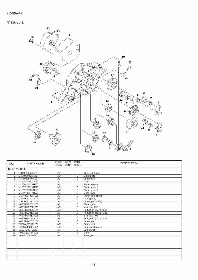
NO. PARTS CODEPRICERANK
NEWMARK
PARTRANK
DESCRIPTION
FO-90AAR
– 5 –
[5] Drive unit
19
1
2
3
18
5
6
7
89
9
11
10
12
12
9
12
91213
13
13
1515
16
17
4
20
21
21
22
14
B3
[5] Drive unit1 LFRM-2206XHZZ AF C Drive unit frame2 LPLTM3049XHZZ AD C Motor plate3 LPLTP3050XHZZ AB C Cutter plate4 MCAMP2027XHZZ AC C Cam5 MLEVP2311XHZZ AB C Planet lever A6 MLEVP2312XHZZ AB C Planet lever B7 MLEVP2313XHZZ AC C Planet lever C8 MLEVP2314XHZZ AB C Mode lever9 MSPRC2735XHZZ AC C Planet gear spring
10 MSPRC3110XHZZ AB C Cam spring11 MSPRC3127XHZZ AB C Cutter gear spring12 NGERH2278XHZZ AC C Planet gear13 NGERH2379XHZZ AC C Idler gear,25Z14 NGERH2380XHZZ AC C Reduction gear,17/36Z15 NGERH2391XHZZ AC C Reduction gear,17/30Z16 NGERH2451XHZZ AB C Idler gear,30Z17 NGERH2475XHZZ AB C Reduction gear,17/43Z18 NGERH2476XHZZ AB C Cutter gear19 QCNW-207AXHZZ AC C Cutter cable20 QCNW-4933XHZZ AC C Cam switch cable21 QSW-F2224SCZZ AE B Cam switch22 RMOTZ2148XHZZ AT B MotorB3 XEBSD30P08000 AA C Screw(3x8)

FO-90AAR
[6] Packing material & Accessories1 TINSS4042XHZZ AS N D Operation manual2 DUNTK468BXHBG AH E Handset3 QCNW-3976XHBG AK C Handset cord4 PHOP-2105XHZZ AD C Original document support5 QCNW-3975XHGY AG C Telephone line cord6 SPAKP296BXHZZ AE D Vinyl cover7 SPAKA287BXHZZ AE D Packing add.,left8 SPAKA288BXHZZ AE D Packing add.,right9 SPAKA289BXHZZ AC D Pad
10 SPAKC225BXHZZ AP N D Packing case11 TLABM358AXHZZ AS N D Box label18 TCADZ2935XHZZ AA D Caution sheet19 SPAKA388BXHZZ AE D Protection sheet,left20 SPAKA389BXHZZ AE D Protection sheet,right21 PGIDM2579XHZZ AE C Paper roll shim,left22 PGIDM2578XHZZ AE C Paper roll shim,right25 TPAPK2238XHZZ AS N S Fax paper(Initial starter roll 10m)
[6] Packing material & Accessories
1011
9
3
5
TAPE
TAPE
AC CORD
1
ORIGINAL DOCUMENTSUPPORT SIDE
4
19
20
25
2
7
6
TAPE
TAPE
8
R
18
(2)
(1)
(4)
(3)
2122
– 6 –
NO. PARTS CODEPRICERANK
NEWMARK
PARTRANK
DESCRIPTION
NO. PARTS CODEPRICERANK
NEWMARK
PARTRANK
DESCRIPTION
FO-90AAR
– 7 –
[7] Control PWB unit1 UBATL2046SCZZ AK B Battery(CR2032T34) [BAT1]2 VCEAGA1HW106M AA C Capacitor(50WV 10µF) [C1]3 VCEAGA1EW476M AA C Capacitor(25WV 47µF) [C3]4 VCEAGA1HW106M AA C Capacitor(50WV 10µF) [C4]5 VCEAGA1EW476M AA C Capacitor(25WV 47µF) [C7]6 VCEAGA1HW106M AA C Capacitor(50WV 10µF) [C9]7 VCEAGA1HW226M AB C Capacitor(50WV 22µF) [C10]8 VCEAGA1EW476M AA C Capacitor(25WV 47µF) [C11]9 VCCCTV1HH100D AA C Capacitor(50WV 10PF) [C105]
10 VCCCTV1HH100D AA C Capacitor(50WV 10PF) [C106]11 VCKYTV1HB102K AA C Capacitor(50WV 1000PF) [C107]12 VCKYTV1HB102K AA C Capacitor(50WV 1000PF) [C108]13 VCKYTV1HB102K AA C Capacitor(50WV 1000PF) [C109]14 VCKYTV1HB102K AA C Capacitor(50WV 1000PF) [C110]15 VCKYTV1CF105Z AB C Capacitor(16WV 1µF) [C111]16 VCKYTV1EF104Z AA C Capacitor(25WV 0.1µF) [C112]17 VCKYTV1EF104Z AA C Capacitor(25WV 0.1µF) [C113]18 VCKYTV1CF105Z AB C Capacitor(16WV 1µF) [C115]19 VCKYTV1CF105Z AB C Capacitor(16WV 1µF) [C116]20 VCKYTV1HB102K AA C Capacitor(50WV 1000PF) [C118]21 VCKYTV1EF104Z AA C Capacitor(25WV 0.1µF) [C119]22 VCKYTV1HB222K AA C Capacitor(50WV 2200PF) [C120]23 VCKYTV1HB222K AA C Capacitor(50WV 2200PF) [C121]24 VCKYTV1HB222K AA C Capacitor(50WV 2200PF) [C122]25 VCKYTV1CF105Z AB C Capacitor(16WV 1µF) [C125]26 VCKYTV1CF105Z AB C Capacitor(16WV 1µF) [C126]27 VCKYTV1EF104Z AA C Capacitor(25WV 0.1µF) [C127]28 VCKYTV1CF105Z AB C Capacitor(16WV 1µF) [C128]29 VCKYTV1CF105Z AB C Capacitor(16WV 1µF) [C129]30 VCKYTV1HB103K AB C Capacitor(50WV 0.01µF) [C130]31 VCKYTV1CF105Z AB C Capacitor(16WV 1µF) [C131]32 VCKYTV1CF105Z AB C Capacitor(16WV 1µF) [C134]33 VCKYTV1EF104Z AA C Capacitor(25WV 0.1µF) [C137]34 VCCCTV1HH220J AA C Capacitor(50WV 22PF) [C139]35 VCCCTV1HH220J AA C Capacitor(50WV 22PF) [C140]36 VCKYTV1HF104Z AA C Capacitor(50WV 0.1µF) [C141]37 VCKYTV1EF104Z AA C Capacitor(25WV 0.1µF) [C144]38 VCKYTV1EF104Z AA C Capacitor(25WV 0.1µF) [C145]39 VCKYTV1CF105Z AB C Capacitor(16WV 1µF) [C146]40 VCKYTV1HB222K AA C Capacitor(50WV 2200PF) [C147]41 VCKYTV1CF105Z AB C Capacitor(16WV 1µF) [C148]42 VCKYTV1CF105Z AB C Capacitor(16WV 1µF) [C149]43 VCKYTV1CF105Z AB C Capacitor(16WV 1µF) [C150]44 VCKYTV1CF105Z AB C Capacitor(16WV 1µF) [C152]45 VCKYTV1CF105Z AB C Capacitor(16WV 1µF) [C153]46 VCKYTV1CF105Z AB C Capacitor(16WV 1µF) [C154]47 VCKYTV1EF104Z AA C Capacitor(25WV 0.1µF) [C155]48 VCKYTV1CF105Z AB C Capacitor(16WV 1µF) [C157]49 VCKYTV1CF105Z AB C Capacitor(16WV 1µF) [C160]50 VCKYTV1EF104Z AA C Capacitor(25WV 0.1µF) [C161]51 VCKYTV1CF105Z AB C Capacitor(16WV 1µF) [C163]52 VCKYTV1HB102K AA C Capacitor(50WV 1000PF) [C164]53 VCKYTV1CF105Z AB C Capacitor(16WV 1µF) [C165]54 VCKYTV1EF104Z AA C Capacitor(25WV 0.1µF) [C166]55 VCKYTV1EF104Z AA C Capacitor(25WV 0.1µF) [C167]56 VCKYTV1EB104K AA C Capacitor(25WV 0.1µF) [C168]57 VCKYTV1CF105Z AB C Capacitor(16WV 1µF) [C169]58 VCKYTV1EF104Z AA C Capacitor(25WV 0.1µF) [C170]59 VCKYTV1CF105Z AB C Capacitor(16WV 1µF) [C171]60 VCKYTV1CF105Z AB C Capacitor(16WV 1µF) [C172]61 VCKYTV1EF104Z AA C Capacitor(25WV 0.1µF) [C173]62 VCKYTV1HB222K AA C Capacitor(50WV 2200PF) [C175]63 VCCCTV1HH180J AA C Capacitor(50WV 18PF) [C176]64 VCCCTV1HH220J AA C Capacitor(50WV 22PF) [C177]65 VCKYTV1CF105Z AB C Capacitor(16WV 1µF) [C178]66 VCCCTV1HH220J AA C Capacitor(50WV 22PF) [C179]67 VCCCTV1HH220J AA C Capacitor(50WV 22PF) [C180]68 VCCCTV1HH220J AA C Capacitor(50WV 22PF) [C181]69 VCKYTV1HB222K AA C Capacitor(50WV 2200PF) [C183]70 RCILZ2145XHZZ AF C Coil(HM601) [C184]71 RCILZ2145XHZZ AF C Coil(HM601) [C185]72 VCKYTV1CF105Z AB C Capacitor(16WV 1µF) [C186]73 VCKYTV1CF105Z AB C Capacitor(16WV 1µF) [C189]74 VCKYTV1HB472K AA C Capacitor(50WV 4700PF) [C190]75 VCKYTV1CF105Z AB C Capacitor(16WV 1µF) [C191]76 VCKYTV1EF104Z AA C Capacitor(25WV 0.1µF) [C192]77 VCCCTV1HH220J AA C Capacitor(50WV 22PF) [C193]78 VCCCTV1HH220J AA C Capacitor(50WV 22PF) [C194]79 VRS-TS2AD000J AA C Resistor(1/10W 0Ω ±5%) [C195]80 VCKYTV1HB102K AA C Capacitor(50WV 1000PF) [C196]

NO. PARTS CODEPRICERANK
NEWMARK
PARTRANK
DESCRIPTION
FO-90AAR
– 8 –
[7] Control PWB unit81 VCKYTV1HB102K AA C Capacitor(50WV 1000PF) [C197]82 VRS-TS2AD000J AA C Resistor(1/10W 0Ω ±5%) [C202]83 VCKYTV1EB104K AA C Capacitor(25WV 0.1µF) [C204]84 VCKYTV1HB102K AA C Capacitor(50WV 1000PF) [C206]85 VRS-TS2AD000J AA C Resistor(1/10W 0Ω ±5%) [C207]86 VCKYTV1HB221K AA C Capacitor(50WV 220PF) [C209]87 VCKYTV1CF105Z AB C Capacitor(16WV 1µF) [C210]88 VCKYTV1EB104K AA C Capacitor(25WV 0.1µF) [C211]89 VCKYTV1CF105Z AB C Capacitor(16WV 1µF) [C212]90 VRS-TS2AD000J AA C Resistor(1/10W 0Ω ±5%) [C213]91 VCKYTV1EB104K AA C Capacitor(25WV 0.1µF) [C214]92 VCKYTV1HB103K AB C Capacitor(50WV 0.01µF) [C215]93 VCKYTV1EF104Z AA C Capacitor(25WV 0.1µF) [C216]94 VCKYTV1HF104Z AA C Capacitor(50WV 0.1µF) [C223]95 VCKYTV1EF104Z AA C Capacitor(25WV 0.1µF) [C224]96 QCNCM7014SC0G AB C Connector(7pin) [CNCIS]97 QCNCM2442SC0B AB C Conector(2pin) [CNCSW]98 QCNCM7014SC0C AA C Connector(3pin) [CNCUT]99 QCNCM705BAF06 AB C Connector(2pin) [CNDR]
100 QCNCM7014SC0B AD C Connector(2pin) [CNFRS]101 QCNCW2500SC1B AF C Connector(12pin) [CNLIUA]102 QCNCW2500SC0D AG C Connector(4pin) [CNLIUB]103 QCNCM7014SC0F AB C Connector(6pin) [CNMT]104 QCNCM7014SC1F AD C Connector(16pin) [CNPN]105 QCNCW2500SC0H AF C Connector(8pin) [CNPW]106 QCNCM2401SC0B AA C Connector(2pin) [CNSP]107 QCNCM7014SC1F AD C Connector(16pin) [CNTH]108 VRS-HT3AA101J AA C Resistor(1W 100Ω ±5%) [D1]109 VHD1SS355//-1 AB B Diode(1SS355) [D2]110 VHD1SS355//-1 AB B Diode(1SS355) [D3]111 VHD1SS355//-1 AB B Diode(1SS355) [D4]112 VHD1SS355//-1 AB B Diode(1SS355) [D5]113 VHDHRW0202B-1 AD C Diode(HRW0202B) [D6]114 QFS-P2010SCZZ AD B IC protector(KAB2402) [FU100]115 VHIULN2003AN/ AE B IC(ULN2003A) [IC1]116 VHITC7WT74FU1 AF B IC(TC7WT74) [IC2]117 VHIFC2FM209V1 BK N B IC(FC200)(Within IC3 and IC5 pair) [IC3]118 VHIKM29W040-1 AV B IC(KM29W040T) [IC4]119 VHIFC2FM209V1 BK N B IC(FM209V)(Within IC3 and IC5 pair) [IC5]120 VHIW24258S7LE AQ B IC(W24258S-70LE) [IC6]121 VHIXC61AN45M1 AE B IC(XC61AN4502ML) [IC7]122 VHIHCF4051M1T AG B IC(HCF4051) [IC9]123 QSOCZ2051SC32 AC C IC socket(32pin) [IC10]124 VHI27020FNY0A BN N B IC,EPROM(2MB) [IC10]125 VHINJM2113M-1 AG B IC(NJM2113) [IC12]126 RCILZ2145XHZZ AF C Coil(HM601) [L100]127 RCILZ2145XHZZ AF C Coil(HM601) [L101]128 RCILZ2145XHZZ AF C Coil(HM601) [L102]129 RCILZ2145XHZZ AF C Coil(HM601) [L103]130 RCILZ2145XHZZ AF C Coil(HM601) [L104]131 RCILZ2145XHZZ AF C Coil(HM601) [L105]132 RCILZ2145XHZZ AF C Coil(HM601) [L106]133 RCILZ2145XHZZ AF C Coil(HM601) [L107]134 RCILZ2145XHZZ AF C Coil(HM601) [L108]135 VRS-TS2AD000J AA C Resistor(1/10W 0Ω ±5%) [L110]136 VRS-TS2AD000J AA C Resistor(1/10W 0Ω ±5%) [L111]137 VHPSG206S//-1 AG B Photo transistor(SG206S) [PI1]138 VHPSG206S//-1 AG B Photo transistor(SG206S) [PI2]139 VS2SA1037KS-1 AB B Transistor(2SA1037KS) [Q2]140 VS2SC2412KS-1 AB B Transistor(2SC2412-K) [Q3]141 VS2SA1037KS-1 AB B Transistor(2SA1037KS) [Q4]142 VSRNC1402//-1 AC B Transistor(RNC1402) [Q7]143 VRD-HT2HY222J AA C Resistor(1/2W 2.2KΩ ±5%) [R1]144 VRD-HT2HY222J AA C Resistor(1/2W 2.2KΩ ±5%) [R2]145 VRS-TS2AD333J AA C Resistor(1/10W 33KΩ ±5%) [R100]146 VRS-TS2AD271J AA C Resistor(1/10W 270Ω ±5%) [R101]147 VRS-TS2AD101J AA C Resistor(1/10W 100Ω ±5%) [R102]148 VRS-TS2AD000J AA C Resistor(1/10W 0Ω ±5%) [R103]149 VRS-TS2AD471J AA C Resistor(1/10W 470Ω ±5%) [R104]150 VRS-TS2AD333J AA C Resistor(1/10W 33KΩ ±5%) [R105]151 VRS-TS2AD471J AA C Resistor(1/10W 470Ω ±5%) [R106]152 VRS-TS2AD333J AA C Resistor(1/10W 33KΩ ±5%) [R107]153 VRS-TS2AD333J AA C Resistor(1/10W 33KΩ ±5%) [R108]154 VRS-TS2AD101J AA C Resistor(1/10W 100Ω ±5%) [R109]155 VRS-TS2AD104J AA C Resistor(1/10W 100KΩ ±5%) [R110]156 VRS-TS2AD104J AA C Resistor(1/10W 100KΩ ±5%) [R111]157 VRS-TS2AD271J AA C Resistor(1/10W 270Ω ±5%) [R113]158 VRS-TS2AD333J AA C Resistor(1/10W 33KΩ ±5%) [R114]159 VRS-TS2AD471J AA C Resistor(1/10W 470Ω ±5%) [R115]160 VRS-TS2AD151J AA C Resistor(1/10W 150Ω ±5%) [R116]

NO. PARTS CODEPRICERANK
NEWMARK
PARTRANK
DESCRIPTION
FO-90AAR
– 9 –
[7] Control PWB unit161 VRS-TS2AD471J AA C Resistor(1/10W 470Ω ±5%) [R117]162 VRS-TS2AD333J AA C Resistor(1/10W 33KΩ ±5%) [R118]163 VRS-TS2AD333J AA C Resistor(1/10W 33KΩ ±5%) [R119]164 VRS-TS2AD471J AA C Resistor(1/10W 470Ω ±5%) [R120]165 VRS-TS2AD333J AA C Resistor(1/10W 33KΩ ±5%) [R121]166 VRS-TS2AD333J AA C Resistor(1/10W 33KΩ ±5%) [R122]167 VRS-TS2AD201J AG C Resistor(1/10W 200Ω ±5%) [R123]168 VRS-TS2AD333J AA C Resistor(1/10W 33KΩ ±5%) [R124]169 VRS-TS2AD271J AA C Resistor(1/10W 270Ω ±5%) [R125]170 VRS-TS2AD271J AA C Resistor(1/10W 270Ω ±5%) [R126]171 VRS-TS2AD271J AA C Resistor(1/10W 270Ω ±5%) [R127]172 VRS-TS2AD223J AA C Resistor(1/10W 22KΩ ±5%) [R128]173 VRS-TS2AD101J AA C Resistor(1/10W 100Ω ±5%) [R129]174 VRS-TS2AD101J AA C Resistor(1/10W 100Ω ±5%) [R130]175 VRS-TS2AD101J AA C Resistor(1/10W 100Ω ±5%) [R131]176 VRS-TS2AD101J AA C Resistor(1/10W 100Ω ±5%) [R132]177 VRS-TS2AD101J AA C Resistor(1/10W 100Ω ±5%) [R133]178 VRS-TS2AD471J AA C Resistor(1/10W 470Ω ±5%) [R134]179 VRS-TS2AD471J AA C Resistor(1/10W 470Ω ±5%) [R135]180 VRS-TS2AD471J AA C Resistor(1/10W 470Ω ±5%) [R137]181 VRS-TS2AD103J AA C Resistor(1/10W 10KΩ ±5%) [R138]182 VRS-TS2AD471J AA C Resistor(1/10W 470Ω ±5%) [R139]183 VRS-TS2AD000J AA C Resistor(1/10W 0Ω ±5%) [R140]184 VRS-TS2AD103J AA C Resistor(1/10W 10KΩ ±5%) [R141]185 VRS-TS2AD333J AA C Resistor(1/10W 33KΩ ±5%) [R142]186 VRS-TS2AD471J AA C Resistor(1/10W 470Ω ±5%) [R143]187 VRS-TS2AD433J AA C Resistor(1/10W 43KΩ ±5%) [R144]188 VRS-TS2AD303J AA C Resistor(1/10W 30KΩ ±5%) [R145]189 VRS-TS2AD203J AA C Resistor(1/10W 20KΩ ±5%) [R146]190 VRS-TS2AD333J AA C Resistor(1/10W 33KΩ ±5%) [R147]191 VRS-TS2AD471J AA C Resistor(1/10W 470Ω ±5%) [R148]192 VRS-TS2AD333J AA C Resistor(1/10W 33KΩ ±5%) [R149]193 VRS-TS2AD103J AA C Resistor(1/10W 10KΩ ±5%) [R150]194 VRS-TS2AD333J AA C Resistor(1/10W 33KΩ ±5%) [R151]195 VRS-TS2AD103J AA C Resistor(1/10W 10KΩ ±5%) [R152]196 VRS-TS2AD101J AA C Resistor(1/10W 100Ω ±5%) [R153]197 VRS-TS2AD101J AA C Resistor(1/10W 100Ω ±5%) [R154]198 VRS-TS2AD223J AA C Resistor(1/10W 22KΩ ±5%) [R156]199 VRS-TS2AD512J AA C Resistor(1/10W 5.1KΩ ±5%) [R157]200 VRS-TS2AD000J AA C Resistor(1/10W 0Ω ±5%) [R159]201 VRS-TS2AD222J AA C Resistor(1/10W 2.2KΩ ±5%) [R160]202 VRS-TS2AD3R0J AA C Resistor(1/10W 3.0Ω ±5%) [R161]203 VRS-TS2AD102J AA C Resistor(1/10W 1.0KΩ ±5%) [R162]204 VRS-TS2AD103J AA C Resistor(1/10W 10KΩ ±5%) [R163]205 VRS-TS2AD103J AA C Resistor(1/10W 10KΩ ±5%) [R164]206 VRS-TS2AD512J AA C Resistor(1/10W 5.1KΩ ±5%) [R165]207 VRS-TS2AD103J AA C Resistor(1/10W 10KΩ ±5%) [R166]208 VRS-TS2AD106J AA C Resistor(1/10W 10MΩ ±5%) [R167]209 VRS-TS2AD105J AA C Resistor(1/10W 1.0MΩ ±5%) [R168]210 VRS-TS2AD121J AA C Resistor(1/10W 120Ω ±5%) [R169]211 VRS-TS2AD000J AA C Resistor(1/10W 0Ω ±5%) [R173]212 VRS-TS2AD000J AA C Resistor(1/10W 0Ω ±5%) [R176]213 VRS-TS2AD000J AA C Resistor(1/10W 0Ω ±5%) [R177]214 VRS-TS2AD474J AA C Resistor(1/10W 470KΩ ±5%) [R183]215 VRS-TS2AD754J AA C Resistor(1/10W 750KΩ ±5%) [R184]216 VRS-TS2AD304J AA C Resistor(1/10W 300KΩ ±5%) [R185]217 VRS-TS2AD104J AA C Resistor(1/10W 100KΩ ±5%) [R186]218 VRS-TS2AD393J AA C Resistor(1/10W 39KΩ ±5%) [R188]219 VRS-TS2AD103J AA C Resistor(1/10W 10KΩ ±5%) [R189]220 VRS-TS2AD102J AA C Resistor(1/10W 1.0KΩ ±5%) [R190]221 VRS-TS2AD000J AA C Resistor(1/10W 0Ω ±5%) [R192]222 VRS-TS2AD000J AA C Resistor(1/10W 0Ω ±5%) [R193]223 VRS-TS2AD473J AA C Resistor(1/10W 47KΩ ±5%) [R196]224 VRS-TS2AD000J AA C Resistor(1/10W 0Ω ±5%) [R197]225 VRS-TS2AD104J AA C Resistor(1/10W 100KΩ ±5%) [R198]226 VRS-TS2AD153J AA C Resistor(1/10W 15KΩ ±5%) [R199]227 VRS-TS2AD104J AA C Resistor(1/10W 100KΩ ±5%) [R201]228 VRS-TS2AD204J AA C Resistor(1/10W 200KΩ ±5%) [R202]229 VRS-TS2AD302J AA C Resistor(1/10W 3KΩ ±5%) [R203]230 VRS-TS2AD103J AA C Resistor(1/10W 10KΩ ±5%) [R204]231 VRS-TS2AD203J AA C Resistor(1/10W 20KΩ ±5%) [R205]232 VRS-TS2AD474J AA C Resistor(1/10W 470KΩ ±5%) [R208]233 VRS-TS2AD203J AA C Resistor(1/10W 20KΩ ±5%) [R209]234 VRS-TS2AD224J AA C Resistor(1/10W 220KΩ ±5%) [R210]235 VRS-TS2AD562J AA C Resistor(1/10W 5.6KΩ ±5%) [R211]236 VRS-TS2AD271J AA C Resistor(1/10W 270Ω ±5%) [R213]237 VRS-TS2AD271J AA C Resistor(1/10W 270Ω ±5%) [R214]238 VRS-TS2AD271J AA C Resistor(1/10W 270Ω ±5%) [R215]239 VRS-TS2AD271J AA C Resistor(1/10W 270Ω ±5%) [R216]240 VRS-TS2AD271J AA C Resistor(1/10W 270Ω ±5%) [R217]
NO. PARTS CODEPRICERANK
NEWMARK
PARTRANK
DESCRIPTION
FO-90AAR
[7] Control PWB unit241 VRS-TS2AD271J AA C Resistor(1/10W 270Ω ±5%) [R218]242 VRS-TS2AD333J AA C Resistor(1/10W 33KΩ ±5%) [R219]243 VRS-TS2AD333J AA C Resistor(1/10W 33KΩ ±5%) [R220]244 RR-TZ3017SCZZ AC C Block resistor(270Ωx4) [RA1]245 RR-TZ3018SCZZ AC C Block resistor(470Ωx4) [RA2]246 RR-TZ3017SCZZ AC C Block resistor(270Ωx4) [RA3]247 RR-TZ3017SCZZ AC C Block resistor(270Ωx4) [RA4]248 RR-TZ3018SCZZ AC C Block resistor(470Ωx4) [RA5]249 RR-TZ3017SCZZ AC C Block resistor(270Ωx4) [RA6]250 RR-TZ3017SCZZ AC C Block resistor(270Ωx4) [RA7]251 RR-TZ3017SCZZ AC C Block resistor(270Ωx4) [RA8]252 RR-TZ3018SCZZ AC C Block resistor(470Ωx4) [RA9]253 RR-TZ3018SCZZ AC C Block resistor(470Ωx4) [RA10]254 RR-TZ3018SCZZ AC C Block resistor(470Ωx4) [RA11]255 RR-TZ3017SCZZ AC C Block resistor(270Ωx4) [RA12]256 RR-TZ3017SCZZ AC C Block resistor(270Ωx4) [RA13]257 RR-TZ3018SCZZ AC C Block resistor(470Ωx4) [RA14]258 RR-TZ3018SCZZ AC C Block resistor(470Ωx4) [RA15]259 RR-TZ3018SCZZ AC C Block resistor(470Ωx4) [RA16]260 VHI62FP332P-1 AF B IC(XC62FP3302P) [REQ100]261 RRLYD3138XHZZ AG B Relay(DQ1U24VDC) [RY1]262 RCRSQ2157SCZZ AF B Crystal(32.256MHz) [X1]263 RCRSB0297AFZZ AD B Crystal(32.768kHz) [X2]
(Unit)901 DCEKC686NXHZZ BA N E Control PWB unit(Within ROM)
[8] TEL/LIU PWB unit1 VHVDSS301L/-U AF B Varistor(DSS-301L) [AR1]2 QCNW-4753XHZZ AE C Cable [ARG]3 RC-FZ2023SCZZ AF C Capacitor(250WV 1.5µF) [C2]4 RC-FZ3028SCZZ AG C Capacitor(250WV 0.56µF) [C3]5 VCEAGA1HW106M AA C Capacitor(50WV 10µF) [C4]6 VCEAGA1HW475M AA C Capacitor(50WV 4.7µF) [C5]7 VCEAGA1HW226M AB C Capacitor(50WV 22µF) [C6]8 VCEAGA1HW106M AA C Capacitor(50WV 10µF) [C7]9 VCEAGA1HW226M AB C Capacitor(50WV 22µF) [C10]
10 VCEAGA1HW107M AA C Capacitor(50WV 100µF) [C12]11 VCEAGA1HW107M AA C Capacitor(50WV 100µF) [C13]12 VCKYTQ1HB223K AB C Capacitor(50WV 0.022µF) [C103]13 VCKYTV1HB103K AB C Capacitor(50WV 0.01µF) [C104]14 VCKYTV1HB103K AB C Capacitor(50WV 0.01µF) [C105]15 VCKYTV1HB473K AA C Capacitor(50WV 0.047µF) [C106]16 VCKYTV1HB102K AA C Capacitor(50WV 1000PF) [C107]17 VCKYTV1HB152K AA C Capacitor(50WV 1500PF) [C108]18 VCKYTV1HB221K AA C Capacitor(50WV 220PF) [C109]19 VCKYTV1HF104Z AA C Capacitor(50WV 0.1µF) [C110]20 VCKYTV1HB102K AA C Capacitor(50WV 1000PF) [C111]21 VCKYTV1HF104Z AA C Capacitor(50WV 0.1µF) [C112]22 VCKYTV1HB102K AA C Capacitor(50WV 1000PF) [C113]23 VCKYTV1HF104Z AA C Capacitor(50WV 0.1µF) [C114]24 VCCCTV1HH101J AA C Capacitor(50WV 100PF) [C115]25 VCKYTV1HF104Z AA C Capacitor(50WV 0.1µF) [C117]26 VCKYTV1HF104Z AA C Capacitor(50WV 0.1µF) [C118]27 VCKYTV1HB821K AA C Capacitor(50WV 820PF) [C120]28 VCKYTV1HB102K AA C Capacitor(50WV 1000PF) [C121]29 VRS-TS2AD000J AA C Resistor(1/10W 0Ω ±5%) [C122]30 VCKYTQ1HB333K AA C Capacitor(50WV 0.033µF) [C123]31 VRS-TS2AD000J AA C Resistor(1/10W 0Ω ±5%) [C124]32 VCKYTQ1HB104K AB C Capacitor(50WV 0.1µF) [C125]33 VCKYTQ1HB223K AB C Capacitor(50WV 0.022µF) [C126]34 VRS-TS2AD000J AA C Resistor(1/10W 0Ω ±5%) [C127]
! 35 RRLYZ3427SCZZ AN B Relay [CML2]36 QJAKZ2079XH0D AD C Jack [CNHJ]37 QCNCM2548SC1B AH C Connector(12pin) [CNLIUA]38 QCNCM2548SC0D AF C Connector(4pin) [CNLIUB]39 QJAKZ2060SC0B AD C Jack [CNLNJ]40 QJAKZ2060SC0B AD C Jack [CNTLJ]42 VHDDSS133//-1 AA B Diode(1SS133) [D1]43 VHDDSS133//-1 AA B Diode(1SS133) [D2]44 VHDDSS133//-1 AA B Diode(1SS133) [D3]45 VHDDSS133//-1 AA B Diode(1SS133) [D4]46 QSW-Z2263XHZZ AG B Hook switch [HOOK SW]47 VHINJM2904M-2 AG B IC(NJM2904M) [IC101]48 VHINJM2904M-2 AG B IC(NJM2904M) [IC102]49 RCILZ2120SCZZ AD C Coil(4.7mH) [L5]50 RFILN2027XHZZ AC C Coil(R-5C) [L6]
– 10 –

NO. PARTS CODEPRICERANK
NEWMARK
PARTRANK
DESCRIPTION
FO-90AAR
[8] TEL/LIU PWB unit51 RFILN2027XHZZ AC C Coil(R-5C) [L7]52 RFILN2027XHZZ AC C Coil(R-5C) [L8]
! 53 VHPTLP627//-1 AH B Photo coupler(TLP627) [PC1]! 54 VHPTLP521-1BL AE B Photo coupler(TLP521) [PC2]! 55 VHPTLP521-1BL AE B Photo coupler(TLP521) [PC5]
56 VSBS108////-1 AE B FET(BS108) [Q1]57 VS2SC2412KR-1 AD B Transistor(2SC2412K) [Q101]58 VSRNC1402//-1 AC B Transistor(RNC1402) [Q104]59 VSRNC1402//-1 AC B Transistor(RNC1402) [Q105]60 VSRNC1402//-1 AC B Transistor(RNC1402) [Q106]61 VSRNC1402//-1 AC B Transistor(RNC1402) [Q107]62 VRD-HT2HY223J AA C Resistor(1/2W 22KΩ ±5%) [R3]63 VRS-TS2AD433J AA C Resistor(1/10W 43KΩ ±5%) [R101]64 VRS-TP2BD150J AA C Resistor(1/8W 15Ω ±5%) [R102]65 VRS-TS2AD000J AA C Resistor(1/10W 0Ω ±5%) [R103]66 VRS-TS2AD103J AA C Resistor(1/10W 10KΩ ±5%) [R104]67 VRS-TS2AD153J AA C Resistor(1/10W 15KΩ ±5%) [R105]68 VRS-TP2BD150J AA C Resistor(1/8W 15Ω ±5%) [R107]69 VRS-TS2AD152J AA C Resistor(1/10W 1.5KΩ ±5%) [R108]70 VRS-TS2AD102J AA C Resistor(1/10W 1KΩ ±5%) [R109]71 VRS-TS2AD512J AA C Resistor(1/10W 5.1KΩ ±5%) [R110]72 VRS-TS2AD203J AA C Resistor(1/10W 20KΩ ±5%) [R111]73 VRS-TS2AD102J AA C Resistor(1/10W 1KΩ ±5%) [R112]74 VRS-TS2AD203J AA C Resistor(1/10W 20KΩ ±5%) [R113]75 VRS-TS2AD563J AA C Resistor(1/10W 56KΩ ±5%) [R114]76 VRS-TS2AD204J AA C Resistor(1/10W 200KΩ ±5%) [R115]77 VRS-TS2AD332J AA C Resistor(1/10W 3.3KΩ ±5%) [R116]78 VRS-TS2AD101J AA C Resistor(1/10W 100Ω ±5%) [R117]79 VRS-TS2AD101J AA C Resistor(1/10W 100Ω ±5%) [R118]80 VRS-TS2AD471J AA C Resistor(1/10W 470Ω ±5%) [R119]81 VRS-TS2AD471J AA C Resistor(1/10W 470Ω ±5%) [R120]82 VRS-TS2AD104J AA C Resistor(1/10W 100KΩ ±5%) [R122]83 VRS-TS2AD151J AA C Resistor(1/10W 150Ω ±5%) [R123]84 VRS-TS2AD222J AA C Resistor(1/10W 2.2KΩ ±5%) [R124]85 VRS-TS2AD332J AA C Resistor(1/10W 3.3KΩ ±5%) [R125]86 VRS-TS2AD823J AA C Resistor(1/10W 82KΩ ±5%) [R126]87 VRS-TS2AD243J AA C Resistor(1/10W 24KΩ ±5%) [R127]88 VRS-TS2AD822J AA C Resistor(1/10W 8.2KΩ ±5%) [R128]89 VRS-TS2AD621J AA C Resistor(1/10W 620Ω ±5%) [R129]90 VRS-TS2AD000J AA C Resistor(1/10W 0Ω ±5%) [R130]91 VRS-TS2AD332J AA C Resistor(1/10W 3.3KΩ ±5%) [R131]92 VRS-TS2AD000J AA C Resistor(1/10W 0Ω ±5%) [R132]93 VRS-TS2AD271J AA C Resistor(1/10W 270Ω ±5%) [R133]94 VRS-TS2AD223J AA C Resistor(1/10W 22KΩ ±5%) [R134]95 VRS-TS2AD102J AA C Resistor(1/10W 1KΩ ±5%) [R135]96 VRS-TS2AD222J AA C Resistor(1/10W 2.2KΩ ±5%) [R137]97 VRS-TS2AD271J AA C Resistor(1/10W 270Ω ±5%) [R138]98 VRS-TS2AD511J AA C Resistor(1/10W 510Ω ±5%) [R139]99 VRS-TS2AD223J AA C Resistor(1/10W 22KΩ ±5%) [R140]
100 VRS-TS2AD473J AA C Resistor(1/10W 47KΩ ±5%) [R141]101 VRS-TS2AD332J AA C Resistor(1/10W 3.3KΩ ±5%) [R142]102 VRS-TS2AD243J AA C Resistor(1/10W 24KΩ ±5%) [R143]103 VRS-TS2AD103J AA C Resistor(1/10W 10KΩ ±5%) [R144]104 RH-DX2007SCZZ AC B Diode bridge(S1ZB60) [REC1]
! 105 RTRNI2165XHZZ AG B Transformer [T1]106 VHVRA501PV6-1 AE B Varistor(RA-501P-V6-2) [VA1]107 VHVRA501PV6-1 AE B Varistor(RA-501P-V6-2) [VA2]108 VHEMTZJ6R8B-1 AC B Zener diode(MTZJ6R8B) [ZD1]109 VHEMTZJ300B-1 AA B Zener diode(MTZJ30B) [ZD2]110 VHEMTZJ200B-1 AC B Zener diode(MTZJ20B) [ZD4]111 VHEMTZJ4R7B-1 AC B Zener diode(MTZJ4R7B) [ZD7]112 VHEMTZJ4R7B-1 AC B Zener diode(MTZJ4R7B) [ZD8]
(Unit)901 DCEKL483BXH11 BD E TEL/Liu PWB unit
[9] Power supply PWB unit1 0CBUGFM224KR/ AF C Capacitor(RE224-C) [C1]2 0CBUGZ1072ZZ/ AN C Capacitor(KMF400VB68M) [C2]3 0CBUGCV102HZ/ AD C Capacitor(ECKZ3D102KBP) [C3]4 0CBUGXAEF222/ AC C Capacitor(GRM40B222K50PT) [C4]5 0CBUEXCAO000/ AB C Resistor(MCR10EZHJ000) [C6]6 0CBUGCM392BJ/ AF C Capacitor(DE1510-1E392M-KX) [C7]7 0CBUGAE561TS/ AH C Capacitor(LXJ35VB560(M)) [C8]8 0CBUGFF474JA/ AF C Capacitor(ECQV1H474JL3) [C9]9 0CBUGAC222VV/ AK C Capacitor(LXZ16VB2200(K)) [C10]
10 0CBUGXAED104/ AC C Capacitor(GRM40B104K25PT) [C12]11 0CBUGZ1041ZZ/ AF C Capacitor(DE1007E222M-KH) [C15]12 0CBUGAB101RV/ AF C Capacitor(KME10VB100(M)) [C16]13 0CBUGXAEF102/ AC C Capacitor(GRM40B102K50PT) [C17]14 0CBUGCU681BR/ AC C Capacitor(DEO805R681K1K-MHR) [C21]
– 11 –

NO. PARTS CODEPRICERANK
NEWMARK
PARTRANK
DESCRIPTION
FO-90AAR
– 12 –
[9] Power supply PWB unit15 0CBUGFF223EH/ AC C Capacitor(AMZV-223J50) [C24]16 0CBPKZ0194ZZ/ AC C Base post ass’y(B 2P3-VH) [CN1]17 0CBPCZ0275ZZ/ AD C Connector(8PL-FJ) [CN2]18 0CBUBC0125DK/ AD B Diode(ERA15-06) [D1]19 0CBUBC0125DK/ AD B Diode(ERA15-06) [D2]20 0CBUBC0125DK/ AD B Diode(ERA15-06) [D3]21 0CBUBC0125DK/ AD B Diode(ERA15-06) [D4]22 0CBUBY0020AK/ AD B Diode(1SS355) [D5]23 0CBUBC0336AZ/ AL B Diode(S3L20U-4004P15) [D7]24 0CBUBC0302BZ/ AE B Diode(SR140) [D8]25 0CBPJCEJ1601/ AH A Current fuse(21501.6 ME600) [F1]26 0CBPJCEJ1601/ AH A Current fuse(21501.6 ME600) [F2]27 0CBPZZ0906ZZ/ AH A Circuit protect chip(CCP2E100) [F3]28 0CBBFZ89256Z/ AD B Beads core(BL02RNI-R62T4) [FB1]29 0CBUCB0199AZ/ AR B IC(UPC29M05AHF) [IC1]30 0CBUKZ0826ZZ/ AK C Filter(ELF15N003A) [L1]31 0CBUZZ0156ZZ/ AN C Coil(RS208) [L2]32 0CBPZZ0940ZZ/ AB C Jumper(J1/6Z-T26-A) [L3]33 0CBLRZ6616ZN/ AQ C Heat sink(MN903-5001AT) [MT1]34 0CBLRZ6619ZQ/ AQ C Heat sink(MF903-5002AT) [MT2]35 0CBUDC0163CZ/ AG B Photo coupler(PC123YS) [PC1]36 0CBUDC0163CZ/ AG B Photo coupler(PC123YS) [PC2]37 0CBUAG0161AC/ AQ B FET(FS5KM-18A-AN) [Q1]38 0CBUDA0128AK/ AD B Transistor(2SD2114K) [Q2]39 0CBUAY0016CK/ AD B Transistor(2SC2412K) [Q3]40 0CBUAY0016CK/ AD B Transistor(2SC2412K) [Q4]41 0CBUAC0289AK/ AD B Transistor(2SC4210) [Q5]42 0CBUAC0289AK/ AD B Transistor(2SC4210) [Q6]43 0CBUEEC335CH/ AC C Resistor(RDM12TB335J) [R1]44 0CBUEEC105CH/ AC C Resistor(RDM12TB105J) [R2]45 0CBUEEC105CH/ AC C Resistor(RDM12TB105J) [R3]46 0CBUEXCAS331/ AB C Resistor(CR21TR331J) [R4]47 0CBUEXCAS152/ AB C Resistor(CR21TR152J) [R5]48 0CBUEXCAS183/ AB C Resistor(CR21TR183J) [R6]49 0CBUEXCAS330/ AB C Resistor(CR21TR330J) [R7]50 0CBUEXCAS473/ AB C Resistor(CR21TR473J) [R8]51 0CBUEXCAS471/ AB C Resistor(CR21TR471J) [R9]52 0CBUEFDR33DB/ AE C Resistor(RSMF1TBR33G) [R10]53 0CBUEXCAS390/ AB C Resistor(CR21TR390J) [R11]54 0CBUEXCAS184/ AB C Resistor(CR21TR184J) [R12]55 0CBUEXCAS472/ AB C Resistor(CR21TR472J) [R13]56 0CBUEXCAS152/ AB C Resistor(CR21TR152J) [R14]57 0CBUEXCAS334/ AB C Resistor(CR21TR334J) [R15]58 0CBUEXCAS223/ AB C Resistor(CR21TR223J) [R16]59 0CBUEXCAS822/ AB C Resistor(CR21TR822J) [R17]60 0CBUEXCAS273/ AB C Resistor(CR21TR273J) [R18]61 0CBUEXCAS472/ AB C Resistor(CR21TR472J) [R19]62 0CBUEXCAS472/ AB C Resistor(CR21TR472J) [R20]63 0CBUEXCAS154/ AB C Resistor(CR21TR154J) [R21]64 0CBUEXCAS103/ AB C Resistor(CR21TR103J) [R25]65 0CB829655027/ BE B Transformer(PTTP124-KTT) [T1]66 0CBUDC0232AK/ AF B Thermistor(KL07L8R2TB) [TH1]67 0CBUEZ0507ZZ/ AD B Varistor(ERZV07D471) [V1]68 0CBUFBA102FE/ AD B Variable resistor(ENV CYA A01 B13) [VR1]69 0CBUBDAX270A/ AD B Zener diode(RD27SB) [ZD1]70 0CBUBXAD2R0A/ AD B Zener diode(RD2.0SB) [ZD2]71 0CBUBDBM300D/ AC B Zener diode(RD30FB) [ZD4]72 0CBUBXAD6R2C/ AD B Zener diode(RD6.2SB) [ZD5]73 0CBUBDBE200D/ AD B Zener diode(RD20ESAB) [ZD7]
(Unit)! 901 RDENT2144XHZZ BA E Power supply PWB unit

No. NEWMARK
PARTRANK
PRICERANKPARTS CODE No. NEW
MARKPARTRANK
PRICERANKPARTS CODENo. NEW
MARKPARTRANK
PRICERANKPARTS CODE
FO-90AAR
– 13 –
I n d e x
[C]CCNW-212AXH01 1-2 AK C
″ 3-1 AK CCCNW-215AXH01 1-12 AG C
[D]DCEKC686NXHZZ 1-45 BA N E
″ 7-901 BA N EDCEKL483BXH11 1-16 BD E
″ 8-901 BD EDCEKP481BXH52 1-1 BB N E
″ 3-901 BB N EDCEKP482BXH03 3-7 BB N EDUNTK468BXHBG 6-2 AH E
[G]GCABA2342XHSM 3-3 AH N DGCABB2343XHSA 1-13 AK DGCASP2110XHSD 1-17 AK CGCASP2111XHSA 1-18 AH CGDAI-2082XHSA 1-46 AD CGDAI-2083XHZZ 1-22 AF C
[H]HPNLH2393XHSC 1-54 AF N D
[J]JBTN-2257XHSA 3-4 AD CJBTN-2258XHSA 3-5 AC CJBTN-2261XHSA 3-6 AC CJBTN-2262XHSA 3-8 AC N C
[L]LBNDJ2006XHZZ 1-55 AA C
″ 2-19 AA CLBSHP2110XHZZ 2-1 AB CLBSHP2112XHZZ 1-28 AB CLFRM-2206XHZZ 5-1 AF CLFRM-2208XHZZ 1-29 AF CLFRM-2209XHZZ 2-2 AF CLHLDZ2180XHZZ 2-3 AC CLHLDZ2181XHZZ 2-4 AC CLHLDZ2184XHZZ 1-30 AC CLHLDZ2185XHZZ 1-31 AC CLPLTG2911XHZZ 4-1 AE CLPLTM3049XHZZ 5-2 AD CLPLTM3107XHZZ 1-63 AD N CLPLTP2908XHZZ 4-2 AE CLPLTP3050XHZZ 5-3 AB CLPLTP3051XHZZ 4-3 AB CLSTPP2054XHZZ 1-47 AC CLX-BZ2138XHZZ 1-B1 AB C
[M]MARMP2023XHZZ 1-48 AB CMCAMP2027XHZZ 5-4 AC CMLEVP2311XHZZ 5-5 AB CMLEVP2312XHZZ 5-6 AB CMLEVP2313XHZZ 5-7 AC CMLEVP2314XHZZ 5-8 AB CMLEVP2315XHZA 1-32 AC N CMLEVP2316XHZZ 1-23 AC CMLEVP2317XHZZ 2-5 AB CMLEVP2319XHZZ 1-49 AC CMLEVP2320XHZZ 1-19 AC CMSPRC2735XHZZ 5-9 AC CMSPRC2954XHZZ 1-5 AC CMSPRC3110XHZZ 5-10 AB CMSPRC3112XHZZ 1-33 AC CMSPRC3117XHZZ 2-6 AB CMSPRC3127XHZZ 5-11 AB CMSPRC3148XHZZ 1-34 AC CMSPRD3115XHZZ 1-35 AB CMSPRD3116XHZZ 1-24 AB CMSPRD3169XHZZ 1-57 AD CMSPRP3119XHZZ 1-14 AC CMSPRP3123XHZZ 1-15 AC CMSPRT3114XHZZ 1-25 AC CMSPRT3139XHZZ 4-5 AA CMSPRT3140XHZZ 4-4 AA C
[N]NGERH2278XHZZ 5-12 AC CNGERH2379XHZZ 5-13 AC CNGERH2380XHZZ 5-14 AC CNGERH2391XHZZ 5-15 AC CNGERH2451XHZZ 5-16 AB C
NGERH2475XHZZ 5-17 AB CNGERH2476XHZZ 5-18 AB CNGERH2477XHZZ 1-50 AC CNGERH2478XHZZ 1-36 AB CNGERH2479XHZZ 2-7 AB CNGERH2480XHZZ 2-8 AB CNGERH2481XHZZ 2-9 AB CNGERP2318XHZZ 1-6 AD CNROLP2426XHZZ 1-26 AC CNROLR2375XHZZ 2-10 AL CNROLR2425XHZZ 1-37 AP CNROLR2427XHZZ 1-42 AC CNROLR2428XHZZ 2-11 AP CNSFTZ2273XHZZ 2-12 AF C
[P]PCUSU2132XHZZ 1-59 AC CPCUT-2040SCZZ 1-51 AV CPGIDM2554XHZZ 4-6 AF CPGIDM2558XHZZ 1-38 AD CPGIDM2559XHSA 1-27 AE CPGIDM2560XHSA 1-7 AC CPGIDM2561XHSA 1-8 AC CPGIDM2562XHZZ 2-13 AD CPGIDM2564XHZZ 1-44 AD CPGIDM2566XHZZ 1-52 AC CPGIDM2578XHZZ 6-22 AE CPGIDM2579XHZZ 6-21 AE CPGUMR2168XHZZ 1-43 AF CPHOP-2104XHSA 1-9 AF CPHOP-2105XHZZ 6-4 AD CPSHEZ3410XHZZ 1-56 AB CPSHEZ3510XHZZ 4-7 AE CPSHEZ3543XHZZ 2-21 AE N C
[Q]QACCR2048XHZZ 1-20 AX BQCNCM2401SC0B 7-106 AA CQCNCM2442SC0B 7-97 AB CQCNCM2548SC0D 8-38 AF CQCNCM2548SC1B 8-37 AH CQCNCM7014SC0B 7-100 AD CQCNCM7014SC0C 7-98 AA CQCNCM7014SC0F 7-103 AB CQCNCM7014SC0G 7-96 AB CQCNCM7014SC1F 7-104 AD C
″ 7-107 AD CQCNCM705BAF06 7-99 AB CQCNCW2500SC0D 7-102 AG CQCNCW2500SC0H 7-105 AF CQCNCW2500SC1B 7-101 AF CQCNW-207AXHZZ 5-19 AC CQCNW-209AXHZZ 1-39 AH CQCNW-210AXHZZ 1-40 AC CQCNW-211AXHZZ 2-15 AF CQCNW-213AXHZZ 2-16 AC CQCNW-352AXHZZ 2-22 AH N CQCNW-3975XHGY 6-5 AG CQCNW-3976XHBG 6-3 AK CQCNW-4753XHZZ 8-2 AE CQCNW-4933XHZZ 5-20 AC CQFS-P2010SCZZ 7-114 AD BQJAKZ2060SC0B 8-39 AD C
″ 8-40 AD CQJAKZ2079XH0D 8-36 AD CQSOCZ2051SC32 7-123 AC CQSW-F2224SCZZ 5-21 AE BQSW-M2293XHZZ 2-17 AE BQSW-M2296XHZZ 1-11 AD BQSW-Z2263XHZZ 8-46 AG B
[R]RC-FZ2023SCZZ 8-3 AF CRC-FZ3028SCZZ 8-4 AG CRCILZ2120SCZZ 8-49 AD CRCILZ2145XHZZ 7-70 AF C
″ 7-71 AF C″ 7-126 AF C″ 7-127 AF C″ 7-128 AF C″ 7-129 AF C″ 7-130 AF C″ 7-131 AF C
RCILZ2145XHZZ 7-132 AF C″ 7-133 AF C″ 7-134 AF C
RCORF2123XHZZ 2-20 AD BRCORF2125XHZZ 1-53 AE BRCRSB0297AFZZ 7-263 AD BRCRSQ2157SCZZ 7-262 AF BRDENT2144XHZZ 1-21 BA E
″ 9-901 BA ERFILN2027XHZZ 8-50 AC C
″ 8-51 AC C″ 8-52 AC C
RH-DX2007SCZZ 8-104 AC BRHEDZ2059XHZZ 1-41 BF BRMOTZ2148XHZZ 5-22 AT BRR-TZ3017SCZZ 7-244 AC C
″ 7-246 AC C″ 7-247 AC C″ 7-249 AC C″ 7-250 AC C″ 7-251 AC C″ 7-255 AC C″ 7-256 AC C
RR-TZ3018SCZZ 7-245 AC C″ 7-248 AC C″ 7-252 AC C″ 7-253 AC C″ 7-254 AC C″ 7-257 AC C″ 7-258 AC C″ 7-259 AC C
RRLYD3138XHZZ 7-261 AG BRRLYZ3427SCZZ 8-35 AN BRTRNI2165XHZZ 8-105 AG BRUNTZ2054XHZZ 2-18 BE B
[S]SPAKA287BXHZZ 6-7 AE DSPAKA288BXHZZ 6-8 AE DSPAKA289BXHZZ 6-9 AC DSPAKA388BXHZZ 6-19 AE DSPAKA389BXHZZ 6-20 AE DSPAKC225BXHZZ 6-10 AP N DSPAKP296BXHZZ 6-6 AE D
[T]TCADZ2935XHZZ 6-18 AA DTINSS4042XHZZ 6-1 AS N DTLABM358AXHZZ 6-11 AS N DTPAPK2238XHZZ 6-25 AS N S
[U]UBATL2046SCZZ 7-1 AK B
[V]VCCCTV1HH100D 7-9 AA C
″ 7-10 AA CVCCCTV1HH101J 8-24 AA CVCCCTV1HH180J 7-63 AA CVCCCTV1HH220J 7-34 AA C
″ 7-35 AA C″ 7-64 AA C″ 7-66 AA C″ 7-67 AA C″ 7-68 AA C″ 7-77 AA C″ 7-78 AA C
VCEAGA1EW476M 7-3 AA C″ 7-5 AA C″ 7-8 AA C
VCEAGA1HW106M 7-2 AA C″ 7-4 AA C″ 7-6 AA C″ 8-5 AA C″ 8-8 AA C
VCEAGA1HW107M 8-10 AA C″ 8-11 AA C
VCEAGA1HW226M 7-7 AB C″ 8-7 AB C″ 8-9 AB C
VCEAGA1HW475M 8-6 AA CVCKYTQ1HB104K 8-32 AB CVCKYTQ1HB223K 8-12 AB C
″ 8-33 AB C

No. NEWMARK
PARTRANK
PRICERANKPARTS CODE No. NEW
MARKPARTRANK
PRICERANKPARTS CODE No. NEW
MARKPARTRANK
PRICERANKPARTS CODE
FO-90AAR
– 14 –
VCKYTQ1HB333K 8-30 AA CVCKYTV1CF105Z 7-15 AB C
″ 7-18 AB C″ 7-19 AB C″ 7-25 AB C″ 7-26 AB C″ 7-28 AB C″ 7-29 AB C″ 7-31 AB C″ 7-32 AB C″ 7-39 AB C″ 7-41 AB C″ 7-42 AB C″ 7-43 AB C″ 7-44 AB C″ 7-45 AB C″ 7-46 AB C″ 7-48 AB C″ 7-49 AB C″ 7-51 AB C″ 7-53 AB C″ 7-57 AB C″ 7-59 AB C″ 7-60 AB C″ 7-65 AB C″ 7-72 AB C″ 7-73 AB C″ 7-75 AB C″ 7-87 AB C″ 7-89 AB C
VCKYTV1EB104K 7-56 AA C″ 7-83 AA C″ 7-88 AA C″ 7-91 AA C
VCKYTV1EF104Z 7-16 AA C″ 7-17 AA C″ 7-21 AA C″ 7-27 AA C″ 7-33 AA C″ 7-37 AA C″ 7-38 AA C″ 7-47 AA C″ 7-50 AA C″ 7-54 AA C″ 7-55 AA C″ 7-58 AA C″ 7-61 AA C″ 7-76 AA C″ 7-93 AA C″ 7-95 AA C
VCKYTV1HB102K 7-11 AA C″ 7-12 AA C″ 7-13 AA C″ 7-14 AA C″ 7-20 AA C″ 7-52 AA C″ 7-80 AA C″ 7-81 AA C″ 7-84 AA C″ 8-16 AA C″ 8-20 AA C″ 8-22 AA C″ 8-28 AA C
VCKYTV1HB103K 7-30 AB C″ 7-92 AB C″ 8-13 AB C″ 8-14 AB C
VCKYTV1HB152K 8-17 AA CVCKYTV1HB221K 7-86 AA C
″ 8-18 AA CVCKYTV1HB222K 7-22 AA C
″ 7-23 AA C″ 7-24 AA C″ 7-40 AA C″ 7-62 AA C″ 7-69 AA C
VCKYTV1HB472K 7-74 AA CVCKYTV1HB473K 8-15 AA CVCKYTV1HB821K 8-27 AA CVCKYTV1HF104Z 7-36 AA C
VCKYTV1HF104Z 7-94 AA C″ 8-19 AA C″ 8-21 AA C″ 8-23 AA C″ 8-25 AA C″ 8-26 AA C
VHDDSS133//-1 8-42 AA B″ 8-43 AA B″ 8-44 AA B″ 8-45 AA B
VHDHRW0202B-1 7-113 AD CVHD1SS355//-1 7-109 AB B
″ 7-110 AB B″ 7-111 AB B″ 7-112 AB B
VHEMTZJ200B-1 8-110 AC BVHEMTZJ300B-1 8-109 AA BVHEMTZJ4R7B-1 8-111 AC B
″ 8-112 AC BVHEMTZJ6R8B-1 8-108 AC BVHIFC2FM209V1 7-117 BK N B
″ 7-119 BK N BVHIHCF4051M1T 7-122 AG BVHIKM29W040-1 7-118 AV BVHINJM2113M-1 7-125 AG BVHINJM2904M-2 8-47 AG B
″ 8-48 AG BVHITC7WT74FU1 7-116 AF BVHIULN2003AN/ 7-115 AE BVHIW24258S7LE 7-120 AQ BVHIXC61AN45M1 7-121 AE BVHI27020FNY0A 7-124 BN N BVHI62FP332P-1 7-260 AF BVHPSG206S//-1 7-137 AG B
″ 7-138 AG BVHPTLP521-1BL 8-54 AE B
″ 8-55 AE BVHPTLP627//-1 8-53 AH BVHVDSS301L/-U 8-1 AF BVHVRA501PV6-1 8-106 AE B
″ 8-107 AE BVRD-HT2HY222J 7-143 AA C
″ 7-144 AA CVRD-HT2HY223J 8-62 AA CVRS-HT3AA101J 7-108 AA CVRS-TP2BD150J 8-64 AA C
″ 8-68 AA CVRS-TS2AD000J 7-79 AA C
″ 7-82 AA C″ 7-85 AA C″ 7-90 AA C″ 7-135 AA C″ 7-136 AA C″ 7-148 AA C″ 7-183 AA C″ 7-200 AA C″ 7-211 AA C″ 7-212 AA C″ 7-213 AA C″ 7-221 AA C″ 7-222 AA C″ 7-224 AA C″ 8-29 AA C″ 8-31 AA C″ 8-34 AA C″ 8-65 AA C″ 8-90 AA C″ 8-92 AA C
VRS-TS2AD101J 7-147 AA C″ 7-154 AA C″ 7-173 AA C″ 7-174 AA C″ 7-175 AA C″ 7-176 AA C″ 7-177 AA C″ 7-196 AA C″ 7-197 AA C″ 8-78 AA C″ 8-79 AA C
VRS-TS2AD102J 7-203 AA C
VRS-TS2AD102J 7-220 AA C″ 8-70 AA C″ 8-73 AA C″ 8-95 AA C
VRS-TS2AD103J 7-181 AA C″ 7-184 AA C″ 7-193 AA C″ 7-195 AA C″ 7-204 AA C″ 7-205 AA C″ 7-207 AA C″ 7-219 AA C″ 7-230 AA C″ 8-66 AA C″ 8-103 AA C
VRS-TS2AD104J 7-155 AA C″ 7-156 AA C″ 7-217 AA C″ 7-225 AA C″ 7-227 AA C″ 8-82 AA C
VRS-TS2AD105J 7-209 AA CVRS-TS2AD106J 7-208 AA CVRS-TS2AD121J 7-210 AA CVRS-TS2AD151J 7-160 AA C
″ 8-83 AA CVRS-TS2AD152J 8-69 AA CVRS-TS2AD153J 7-226 AA C
″ 8-67 AA CVRS-TS2AD201J 7-167 AG CVRS-TS2AD203J 7-189 AA C
″ 7-231 AA C″ 7-233 AA C″ 8-72 AA C″ 8-74 AA C
VRS-TS2AD204J 7-228 AA C″ 8-76 AA C
VRS-TS2AD222J 7-201 AA C″ 8-84 AA C″ 8-96 AA C
VRS-TS2AD223J 7-172 AA C″ 7-198 AA C″ 8-94 AA C″ 8-99 AA C
VRS-TS2AD224J 7-234 AA CVRS-TS2AD243J 8-87 AA C
″ 8-102 AA CVRS-TS2AD271J 7-146 AA C
″ 7-157 AA C″ 7-169 AA C″ 7-170 AA C″ 7-171 AA C″ 7-236 AA C″ 7-237 AA C″ 7-238 AA C″ 7-239 AA C″ 7-240 AA C″ 7-241 AA C″ 8-93 AA C″ 8-97 AA C
VRS-TS2AD3R0J 7-202 AA CVRS-TS2AD302J 7-229 AA CVRS-TS2AD303J 7-188 AA CVRS-TS2AD304J 7-216 AA CVRS-TS2AD332J 8-77 AA C
″ 8-85 AA C″ 8-91 AA C″ 8-101 AA C
VRS-TS2AD333J 7-145 AA C″ 7-150 AA C″ 7-152 AA C″ 7-153 AA C″ 7-158 AA C″ 7-162 AA C″ 7-163 AA C″ 7-165 AA C″ 7-166 AA C″ 7-168 AA C″ 7-185 AA C″ 7-190 AA C

FO-90AAR
SHARP CORPORATIONCommunication Systems GroupQuality & Reliability Control CenterHigashihiroshima, Hiroshima 739-0192, Japan
Printed in Japan
A0004-74NS•IS•T
COPYRIGHT © 2000 BY SHARP CORPORATION
ALL RIGHTS RESERVED.
No part of this publication may be reproduced,stored in a retrieval system, or transmitted inany form or by any means, electronic, mechanical,photocopying, recording, or otherwise, withoutprior written permission of the publisher.
VRS-TS2AD333J 7-192 AA C″ 7-194 AA C″ 7-242 AA C″ 7-243 AA C
VRS-TS2AD393J 7-218 AA CVRS-TS2AD433J 7-187 AA C
″ 8-63 AA CVRS-TS2AD471J 7-149 AA C
″ 7-151 AA C″ 7-159 AA C″ 7-161 AA C″ 7-164 AA C″ 7-178 AA C″ 7-179 AA C″ 7-180 AA C″ 7-182 AA C″ 7-186 AA C″ 7-191 AA C″ 8-80 AA C″ 8-81 AA C
VRS-TS2AD473J 7-223 AA C″ 8-100 AA C
VRS-TS2AD474J 7-214 AA C″ 7-232 AA C
VRS-TS2AD511J 8-98 AA CVRS-TS2AD512J 7-199 AA C
″ 7-206 AA C″ 8-71 AA C
VRS-TS2AD562J 7-235 AA CVRS-TS2AD563J 8-75 AA CVRS-TS2AD621J 8-89 AA CVRS-TS2AD754J 7-215 AA CVRS-TS2AD822J 8-88 AA CVRS-TS2AD823J 8-86 AA CVSBS108////-1 8-56 AE BVSRNC1402//-1 7-142 AC B
″ 8-58 AC B″ 8-59 AC B″ 8-60 AC B″ 8-61 AC B
VS2SA1037KS-1 7-139 AB B″ 7-141 AB B
VS2SC2412KR-1 8-57 AD BVS2SC2412KS-1 7-140 AB B
[X]XBBSD30P06000 1-B4 AA CXBPSN40P06K00 1-B5 AA CXEBSD30P08000 1-B3 AA C
″ 5-B3 AA CXEBSD30P12000 1-B7 AA CXHBSD30P06000 1-B6 AA CXUBSD20P06000 3-B2 AA C
[0]0CBBFZ89256Z/ 9-28 AD B0CBLRZ6616ZN/ 9-33 AQ C0CBLRZ6619ZQ/ 9-34 AQ C0CBPCZ0275ZZ/ 9-17 AD C0CBPJCEJ1601/ 9-25 AH A
″ 9-26 AH A0CBPKZ0194ZZ/ 9-16 AC C0CBPZZ0906ZZ/ 9-27 AH A0CBPZZ0940ZZ/ 9-32 AB C0CBUAC0289AK/ 9-41 AD B
″ 9-42 AD B0CBUAG0161AC/ 9-37 AQ B0CBUAY0016CK/ 9-39 AD B
″ 9-40 AD B0CBUBC0125DK/ 9-18 AD B
″ 9-19 AD B″ 9-20 AD B″ 9-21 AD B
0CBUBC0302BZ/ 9-24 AE B0CBUBC0336AZ/ 9-23 AL B0CBUBDAX270A/ 9-69 AD B0CBUBDBE200D/ 9-73 AD B0CBUBDBM300D/ 9-71 AC B0CBUBXAD2R0A/ 9-70 AD B0CBUBXAD6R2C/ 9-72 AD B0CBUBY0020AK/ 9-22 AD B0CBUCB0199AZ/ 9-29 AR B0CBUDA0128AK/ 9-38 AD B0CBUDC0163CZ/ 9-35 AG B
″ 9-36 AG B0CBUDC0232AK/ 9-66 AF B
0CBUEEC105CH/ 9-44 AC C″ 9-45 AC C
0CBUEEC335CH/ 9-43 AC C0CBUEFDR33DB/ 9-52 AE C0CBUEXCAO000/ 9-5 AB C0CBUEXCAS103/ 9-64 AB C0CBUEXCAS152/ 9-47 AB C
″ 9-56 AB C0CBUEXCAS154/ 9-63 AB C0CBUEXCAS183/ 9-48 AB C0CBUEXCAS184/ 9-54 AB C0CBUEXCAS223/ 9-58 AB C0CBUEXCAS273/ 9-60 AB C0CBUEXCAS330/ 9-49 AB C0CBUEXCAS331/ 9-46 AB C0CBUEXCAS334/ 9-57 AB C0CBUEXCAS390/ 9-53 AB C0CBUEXCAS471/ 9-51 AB C0CBUEXCAS472/ 9-55 AB C
″ 9-61 AB C″ 9-62 AB C
0CBUEXCAS473/ 9-50 AB C0CBUEXCAS822/ 9-59 AB C0CBUEZ0507ZZ/ 9-67 AD B0CBUFBA102FE/ 9-68 AD B0CBUGAB101RV/ 9-12 AF C0CBUGAC222VV/ 9-9 AK C0CBUGAE561TS/ 9-7 AH C0CBUGCM392BJ/ 9-6 AF C0CBUGCU681BR/ 9-14 AC C0CBUGCV102HZ/ 9-3 AD C0CBUGFF223EH/ 9-15 AC C0CBUGFF474JA/ 9-8 AF C0CBUGFM224KR/ 9-1 AF C0CBUGXAED104/ 9-10 AC C0CBUGXAEF102/ 9-13 AC C0CBUGXAEF222/ 9-4 AC C0CBUGZ1041ZZ/ 9-11 AF C0CBUGZ1072ZZ/ 9-2 AN C0CBUKZ0826ZZ/ 9-30 AK C0CBUZZ0156ZZ/ 9-31 AN C0CB829655027/ 9-65 BE B
No. NEWMARK
PARTRANK
PRICERANKPARTS CODE No. NEW
MARKPARTRANK
PRICERANKPARTS CODENo. NEW
MARKPARTRANK
PRICERANKPARTS CODE