ESD instructions for electrical workshops - Theseus
34
Jere Pelkonen ESD instructions for electrical workshops Helsinki Metropolia University of Applied Sciences Bachelor of Engineering Electronics Engineering Thesis 13.05.2017
-
Upload
khangminh22 -
Category
Documents
-
view
0 -
download
0
Transcript of ESD instructions for electrical workshops - Theseus
Jere Pelkonen
ESD instructions for electrical workshops
Helsinki Metropolia University of Applied Sciences
Bachelor of Engineering
Electronics Engineering
Thesis
13.05.2017
Abstract
Author(s) Title Number of Pages Date
Jere Pelkonen ESD instructions for electrical workshops 30 pages 13 May 2017
Degree Bachelors of Engineering
Degree Programme Electronics
Specialisation option
Instructor(s)
Raimo Repo, Project specialist Matti Fischer, Senior Lecturer
The goal of this thesis is writing instructions about Electrostatic Discharge (ESD) protection and how to build Electrostatic Protective Areas (EPA) for an electrical repair workshop use. I am writing these instructions for a company called ABB. ESD protection is needed, when working with any kind of electronics. ESD can damage a sensitive component or a device, making it malfunction, break down completely or defect it so that it will break down prematurely. In this thesis I will explain different ESD control meth-ods and get more into how ESD occurs and why. By doing research from online and literature, the goal was reached. Proper ESD safety in-structions were made.
Keywords ESD, EPA, Static
Contents
1 Introduction 1
2 Theoretical Background on ESD and EPA 2
2.1 ESD 7
2.2 EPA 12
3 ESD Protection 13
3.1 ESD Protective Materials 15
3.2 Protective Gear 16
3.3 ESD Protective Floors 18
3.4 Handling 20
3.5 ESD Measurements and Testing Methods 21
3.6 ESD Training and Auditing 25
4 EPA 26
4.1 Setting up an EPA 26
4.2 Temporary EPA 27
5 Discussion 27
6 Conclusions 28
References 29
Appendices
Appendix 1. Title of the Appendix
Appendix 2. Title of the Appendix

Abbreviations
CDM Charged Device Model
EOS Electrostatic Overstress
EPA Electrostatic Discharge Protected Area
ESD Electrostatic Discharge
ESDS Electrostatic Sensitive Device
DUT Device Under Test
HBM Human Body Model
MM Machine Model
RH Relative Humidity
Appendix 2
1 (30)
1 Introduction
Electrostatic discharge (ESD) is a common issue in the industry field, almost any con-
ceivable industrial process can cause an ESD event. ESD can cause irreversible dam-
age and this is why ESD protection is essential. Especially in the field of electronics and
in industry which manufactures and works on electronics and electric devices. Compo-
nents and integrated circuits that sensitive to ESD affected by it can break down com-
pletely or can be degraded and start malfunctioning later, even passing tests without any
issues. Broken components and circuits increases manufacturing costs, which also af-
fects to product quality and reliability. As technology advances, electronic devices and
what is inside of them become more complex and is fitted in smaller size, their sensitivity
to ESD in general increases. Typically companies have their own ESD safety instructions
but not everyone is aware of the problems it may cause. To put this in perspective there
are many different items, that no one could think of, in workplaces that can carry high
enough charge to damage a circuit. There might be certain tools on your table that can
carry a destructive charge on them. [1].
Therefore ESD being a noticeable problem in the industry field, there is ESD Association
that provides ESD standards. ESD standards are collaboration between all organizations
and individual affected by these standards. ESD standards provide information on re-
quirements, testing methods and technical reports on all ESD related issues. [4].
Electrostatic discharge protected area (EPA) is also a fundamental part of ESD, because
it is a whole area which is protected from static electricity. These areas are built in facto-
ries and repair workshops for ESD safe working ground. [4].
The goal of this thesis is to provide good enough instructions about ESD protection and
information on EPA for ABB’s repair workshops and for the field service engineers. But
also to any other electrical repair workshops that have to take ESD protection under
consideration.
Appendix 2
2 (30)
2 Theoretical Background on ESD and EPA
To get a better grasp on electrostatic discharge and how to control it, understanding how
electrostatic charge occurs, is needed. Electrostatic charge is defined as charge at rest.
Static electricity is all around of us and is a natural phenomenon. A material with no static
charge has equal amount of positive charges being protons and negative charges being
electrons. For static electricity to occur, that material needs to lose or gain electrons. By
bringing two materials into a contact and adding friction, a chemical bond has been cre-
ated between these materials, allowing electrons to move from one material to another.
This happens because charges tend to move from one material to the other to equalize
their electrochemical potential. After separating these materials from one another, some
amount of electrons have left from one material and the equal amount of them has been
gained in the other. Both materials are now electrostatically charged, the one which loses
electrons is now positively charged and the other one gaining electrons is negatively
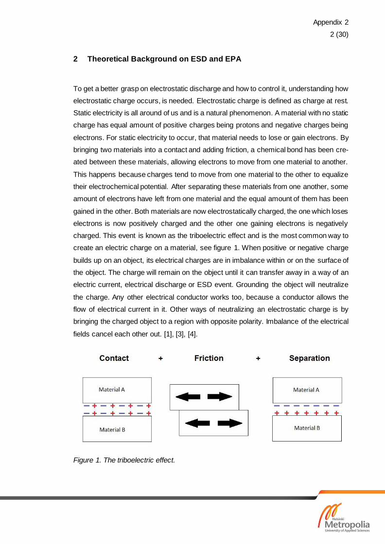
charged. This event is known as the triboelectric effect and is the most common way to
create an electric charge on a material, see figure 1. When positive or negative charge
builds up on an object, its electrical charges are in imbalance within or on the surface of
the object. The charge will remain on the object until it can transfer away in a way of an
electric current, electrical discharge or ESD event. Grounding the object will neutralize
the charge. Any other electrical conductor works too, because a conductor allows the
flow of electrical current in it. Other ways of neutralizing an electrostatic charge is by
bringing the charged object to a region with opposite polarity. Imbalance of the electrical
fields cancel each other out. [1], [3], [4].
Figure 1. The triboelectric effect.
Appendix 2
3 (30)
Static charge created by the triboelectric effect has many other variables affecting the
amount of the charge. The quantity of an electrostatic charge is measured in coulombs.
The quantity of an electrostatic charge on a certain object is denoted as “q”. The elec-
trostatic charge can be calculated by the product of the capacitance of the object, de-
noted as “C”, and the electric potential “V”, on the object. [1].
𝑞 = 𝐶 ∗ 𝑉
Equation 1. Electrostatic charge.
Variables that affect the amount of charge are such as, area of contact, speed of sepa-
ration, relative humidity, roughness and shape of the materials’ contacting surfaces and
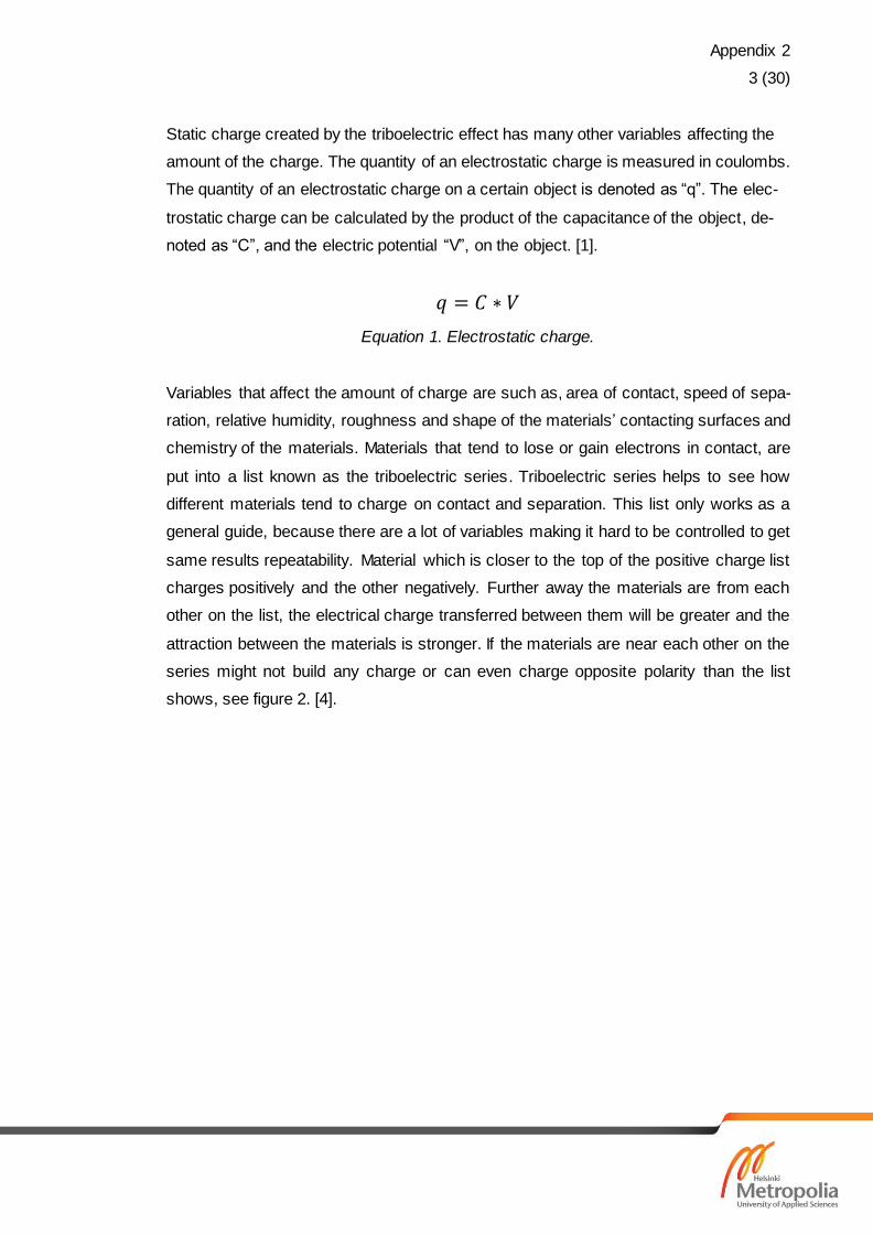
chemistry of the materials. Materials that tend to lose or gain electrons in contact, are
put into a list known as the triboelectric series. Triboelectric series helps to see how
different materials tend to charge on contact and separation. This list only works as a
general guide, because there are a lot of variables making it hard to be controlled to get
same results repeatability. Material which is closer to the top of the positive charge list
charges positively and the other negatively. Further away the materials are from each
other on the list, the electrical charge transferred between them will be greater and the
attraction between the materials is stronger. If the materials are near each other on the
series might not build any charge or can even charge opposite polarity than the list
shows, see figure 2. [4].
Appendix 2
4 (30)
Figure 2. A triboelectric series. [12]
The ways how static charge builds up, can be rather complex. Everything around us af-
fects to the generation of the charge and practically everything can be triboelectrically
charged, even the tiniest impurity particles in the air. Materials’ chemical and physical
characteristics determine how much charge is generated. [3].
Whenever an object builds up an electrical charge, the amount of its electric potential
varies. The electric potential can be calculated by the potential energy “E”, per unit
charge “q”.
𝑉 =𝐸
𝑞
Equation 2. Potential Energy
Value of the electric potential depends how strong the charge is and how much energy
there is in that charge. Different scenarios generate various amounts of electric poten-
tial in each case. Also the relative humidity affects to this. Humid air reduces static
electricity. More humid it is, the more water there is in the air. Water of course conducts
Appendix 2
5 (30)
electricity. So an electrostatically charged object has water molecules on it that shares
its electric potential and reduces it. We will talk about conducting materials and conduc-
tion further in the text. In this next table, there are few examples of electrostatic genera-
tion and the possible potential levels in dry air and humid air, see table 1. These num-
bers are not exact. Because there are many different variating elements, but these give
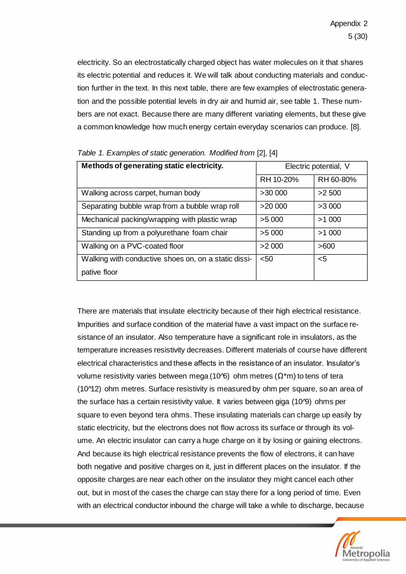
a common knowledge how much energy certain everyday scenarios can produce. [8].
Table 1. Examples of static generation. Modified from [2], [4]
Methods of generating static electricity. Electric potential, V
RH 10-20% RH 60-80%
Walking across carpet, human body >30 000 >2 500
Separating bubble wrap from a bubble wrap roll >20 000 >3 000
Mechanical packing/wrapping with plastic wrap >5 000 >1 000
Standing up from a polyurethane foam chair >5 000 >1 000
Walking on a PVC-coated floor >2 000 >600
Walking with conductive shoes on, on a static dissi-
pative floor
<50 <5
There are materials that insulate electricity because of their high electrical resistance.
Impurities and surface condition of the material have a vast impact on the surface re-
sistance of an insulator. Also temperature have a significant role in insulators, as the
temperature increases resistivity decreases. Different materials of course have different
electrical characteristics and these affects in the resistance of an insulator. Insulator’s
volume resistivity varies between mega (10 6) ohm metres (Ω*m) to tens of tera
(10 12) ohm metres. Surface resistivity is measured by ohm per square, so an area of
the surface has a certain resistivity value. It varies between giga (10 9) ohms per
square to even beyond tera ohms. These insulating materials can charge up easily by
static electricity, but the electrons does not flow across its surface or through its vol-
ume. An electric insulator can carry a huge charge on it by losing or gaining electrons.
And because its high electrical resistance prevents the flow of electrons, it can have
both negative and positive charges on it, just in different places on the insulator. If the
opposite charges are near each other on the insulator they might cancel each other
out, but in most of the cases the charge can stay there for a long period of time. Even
with an electrical conductor inbound the charge will take a while to discharge, because

Appendix 2
6 (30)
there are only a small number of charge carriers which can carry current and by this
discharge the insulator. [9].
Conductive materials on the other hand are materials that have low electrical re-
sistance, which allows electrons to flow easily. Conductors’ resistance and conduct-
ance depends on length of the conductor, the cross-section area of the conductor,
electrical conductivity and electrical resistivity. The resistance varies from hundred
ohms to hundred kilo (10 3) ohms. Temperature also has a relatively small factor in
this one. A conductive material once charged, can only be either positively or nega-
tively charged. Fast flow of electrons will try to keep the conductor at neutral state.
Bringing a neutral conductor in contact to a charged one, the neutral conductor will
even the electrical imbalance within the charged one rapidly. Also connecting conduc-
tor to any electrical grounding point, will neutralize the charge. [4], [10].
A mixture of these two materials is called static dissipative material. Its electrical re-
sistance is somewhere between insulative and conductive materials. Electron flow in
dissipative material depends mainly on its resistance. If the compounds resistivity is
closer to insulative material’s resistance, the electron flow will be really slow and it will
act like and insulator, and if closer to conductive material’s resistance it acts like a con-
ductor. Static dissipative materials can also carry an electrical charge and can be
charged triboelectrically. Dissipative material works like a conductor, it will try to even
the charges within if there are a neutral conductor or grounding point. The transfer of
charge, takes longer compared to same sized conductive material, but faster than insu-
lative material. Because of this, a static dissipative material is widely used in protection
for ESD. It conducts excess charge quickly, but the conductivity is not too high to be
able to create high enough currents to be harmful or swift discharges. [1].
If a material is electrically charged, this means it has an electrostatic field around it.
These electrostatic fields can be measured and calculated. Electric field strength “E”
can is equal to force, denoted as “F”, divided by the charge, denoted as “q”.
=
𝑞
Equation 3. Electric field strength.
Appendix 2
7 (30)
Electric field strength “E” and force “F” are vector quantities. Charge “q” does not have
a line of force associated with it. If the line of force from the electric field is away from
the charge it is positive and if towards then negative. The electric field strength de-
creases by the distance. [4].
Conductive objects can be polarized by bringing them in the region of a charged ob-
ject’s electrostatic field. This phenomenon is called induction. On the surface of the
conductive object the electron will either repel away from the electric field or be at-
tracted closer to the source of the electric field. If the field is negative, negative elec-
trons will be pushed further away from the source, and if the field is positive then it will
attract the electrons closer, trying to even the positive charge of the source. In either
case the conductive material is now polarized, it has negative charge at one end and
positive at the other. Now if we connect this conductive material to a grounding point,
the charge will try to fix electrical imbalance within and the charge will flow from or to
ground. After disconnecting conductive material from the ground and removing the
electrical field, an electrical charge will remain on the object. This is a way of generat-
ing an electric potential on an object, with the help of electrostatic fields. Only conduc-
tive and dissipative materials can be charged by induction. An electrostatic-sensitive
devices can often be damaged by this, if the device is in the field of excess charges
and is then touched with a metallic tool, allowing the excess charges to burst into the
device through this conductor. [3].
2.1 ESD
Electrostatic discharge, as can be reasoned from the name, a swift transfer of static
electricity by a high electrostatic field. So something that has an electrical charge
quickly loses it by discharging the excess charge into something. Bringing and electri-
cally charged object near an electrically neutral object, will charge the neutral object.
Neutral object will be either positively or negatively charged, depending on the charged
object’s polarity. In contact the dielectric between them breaks down and the charged
object discharge to the neutral object. This will create an electric spark, which is usually
visible to human eye, but in some cases the electrical charge is not high enough to be
seen. Over 3000 volt discharges can be felt, over 4000 volt discharges can be heard
and over 5000 volt discharges can be seen. When driving a car you can notice this.
During the travel, you and the seat of the car will start to charge electrically by your
Appendix 2
8 (30)
movement and the two different materials rubbing each other. You are now positively
or negatively charged depends on the material you are wearing, When you reach your
destination and get out of the car, you might be able to feel a zap when touching car’s
door or frame, the electric charge that has been charging up while you were driving has
now discharged. [9].
ESD can change the electrical characteristics of a semiconductor device which damages
the device. Sometimes ESD event may cause a temporal malfunction or a failure on
electronic system, not breaking it. Charged surfaces can work as magnets for impurities
by attracting and holding them, making removal of the particles difficult. These impurities
can carry an electrical charge of their own and possibly damage highly sensitive compo-
nents, such as silicon wafers or even electrical circuitry. [9].
As mentioned before, ESD damage can be instantaneous or an electrostatic sensitive
device “ESDS” has been exposed to an ESD event and will break down later, without
showing any symptoms before. It is good to remember to keep the ESD protection on
from manufacturing to the moment at a repair site handling electronical devices. If there
is a break in the ESD protection somewhere between that time, no one can guarantee
that it should work properly. [10].
An ESD event can do such a damage that an electronic device will instantaneously stop
functioning, this is often denoted as catastrophic failure. Such damage is caused by high
burst of electricity and the deficiency of shielding against high spikes of electricity. High
volume of electricity in a burst can melt metal, fry components, breakdown junctions any
of these can be a cause for an electronic device to stop working. [2].
There can also be scenarios where an electronic device is exposed to an ESD event,
but will keep functioning like intended and breakdown later. This kind of scenario is usu-
ally referred as latent defect. These are hard to identify, because a device with a small
defect can pass all the necessary tests, but still be partially degraded and breakdown
prematurely. These defected devices are costly to repair and can create personnel haz-
ards for the person who is plugin in the device. These matters are also costly for the
company producing them, money and reputation wise. [2].

Appendix 2
9 (30)
A catastrophic failure is rather easy to spot via tests. There are different kind of tests for
different kind of features, but everything is tested from components to electronic devices
before shipping. These tests will prevent the shipping of faulty devices. Latent defects
being really hard to detect, can pass these tests and move forward without any prove of
deficiency. Maybe as the technology advances, we have the correct tools to be able to
spot these invisible defects someday. [2].
There are several different causes for ESD events, in this report I have talked about
static electricity and electrostatic induction. These events are the cause of an ESD dam-
age. An ESD event that causes damage can be an electrostatic discharge to the ESDS,
an electrostatic discharge from the ESDS or by an electrostatic induction, meaning elec-
trostatic fields and their disturbance by an ESDS. Electrostatic discharge’s potential var-
ies by different variables during ESD event. ESDS might be damaged by the discharge
if it has not enough safety measures build in it. The energy transferred during the ESD
event must be evenly distributed along the circuitry otherwise it will cause an electrostatic
overstess “EOS” event, which also damages the device. Other factor is the voltage level
of the charge that varies from few volts to hundreds of kilo volts in some extreme cases.
To bear in mind, many of the ESD events occur without any notice, like a visible spark
or a crackling sound. As small as 10 volts discharge can damage some equipment like
disc drives and circuitry inside of them. How much energy of the discharge and the volt-
age the device can take and when it fails is known as the device’s ESD susceptibility.
[2], [4], [9].
A direct electrostatic discharge from charged conductor to an ESDS is one of the very
common ESD events that causes damage to a sensitive device or component. Human
body works like a conductor and can charge even up to 30 000 volts, when walking
across carpet and the relative humidity in that room is between 10% and 20%. So a
charged human body can work as a carrier of that electrostatic energy. Bringing a hand
near or in a contact with the sensitive device will allow all that energy to discharge, be-
cause the human body is at certain potential and in most of the cases the device is at
very different potential allowing current to flow. Discharge will happen because the
charge on a human body is trying to balance the potential different between these two.
At the discharge human body loses all that excess charge and will be dissipated over
the device and damaging it in most of the cases. There are tests using this same method
but with built circuitry to measure and test ESD susceptibility. It is called the Human Body

Appendix 2
10 (30)
Model “HBM”. Also a metallic tool can work as a conductor and do the same damage, in
this case the event is called the Machine Model “MM”. There are more information about
HBM and MM later in ESD measurement section. [2], [4], [9].
An ESDS can also carry an electrostatic charge which can be discharged to a conductor.
An opposite ESD event of the previous one is another way of causing ESD damage on
sensitive devices or components. Handling, packing, moving are all contact and separa-
tions that accumulate charge on materials. A sensitive device or component on the way
to packing and inside a packing material can start building up a static charge by all this.
Bringing this charged device near a conductor will then discharge and by the swift
change of potentials usually damage the ESDS, causing malfunctions and even break-
downs. This event is also modelled into an ESD susceptibility test and is known as
Charged Device Model (CDM). [2], [4], [9].
Of course as the technology advances and actual human assemblers are less needed
the HBM scenario is not that relevant. But in a field work it is wise to remember that you
have to have everything set up before touching an ESDS. Still with automated production
lines are getting more popular, the ESD is still a common problem because a device may
become charged as it is sliding down a feeder and then is in contact with something that
is very conductive, resulting an ESD event. [2], [4], [9].
An electrostatic induction that also charges materials can be a direct or indirect source
of ESD damage. Whenever an object has accumulated a charge, it also has an electro-
static field. An ESDS inside this electrostatic field will be charged through induction and
be polarized as well. When the charged ESDS is connected to a grounding point it will
discharge similarly as the CDM event was explained. [2], [4], [9].
As mentioned in introduction, standards provide certain guides how to implement ESD
protection in needed place. There are three different categories of these standards. First
one are those that provide ESD control program info and requirements. In my research
ANSI/ESD S20.20 Electrostatic Discharge Control Program Standard stood up and is
being referred to in many different sources and texts. It is a standard that provides ad-
ministrative and technical information about ESD protection and it has different value
limits that should be followed. It was first published in 1999, and was created to provide
much needed information to companies on an ESD control program and how to design,
Appendix 2
11 (30)
develop, implement and maintain it. The ESD control program is to have guide lines how
to protect ESD sensitive electrical equipment, devices or components from being dam-
aged by ESD greater than or equal to 100 volts by human body model or 200 volts by
charged device model. The standard can be applied in any activity that may be suscep-
tible to ESD damage. This standard provides all administrative and technical require-
ments that are needed to build an electrical repair workshop. Administrative require-
ments are, ESD control program plan, training plan requirement and compliance verifi-
cation plan. And the technical requirements are, grounding and bonding systems, per-
sonnel grounding, protected areas, packaging, marking, equipment, handling. Audits are
occasionally performed to verify compliance with these requirements. Audits are efficient
way to see that the ESD protection is up to date and the personnel is following the given
guide lines. [4].
A second standard group is about packaging requirements and grounding. The last
group has standardized test methods and documentation about all already conducted
tests. [4].
ESD susceptibility is determined by testing and measuring how much an ESDS can dis-
sipate discharged energy at ESD event and how high voltage levels it can withstand.
Tests are made by the previously explained ESD event models, according to the wanted
situation. To see how much a certain component or a device can handle when there is a
person working, HBM event could be used. This would help to define the ESD limits and
the correct safety measures. There is no idea of spending millions on correct ESD control
protection, if there is a reasonable set of rules to follow and will do the same job, without
costing a fortune for the company. These models are only test procedures to help choos-
ing the right way to approach same kind of situations, they are not exact copy of a real
time event with other variables around too. There will be more information about the ESD
testing later in this report. [2], [4], [9].
Everything is getting smaller and more complex in digital way, at the same time ESD
problems are increasing, because these smaller components and circuits tend to be
more sensitive to ESD damage and need even higher precautions with them. Already
now there are many items are only susceptible for hundred volts or even below. And as
seen from table 1, those numbers are easily met if there is no ESD protection taken
under consideration. [2], [4], [9], [10].

Appendix 2
12 (30)
2.2 EPA
Electrostatic discharge protected area “EPA”, means an area that has same electric po-
tential between all surfaces, ESDS, people and tools. An EPA is equipped with ESD
controlling items and materials. Having same electric potential between different objects
minimize the risk of an ESD event and prevent sensitive devices and components being
damaged. In ESD protected areas insulating materials are not used, their electrical char-
acteristics are not suitable there. As mentioned before even grounding an insulative ma-
terial will not neutralize the charge immediately and those can build up a huge charge
which is a risk for ESDS. Instead dissipative and conducting materials are used and
everything inside an EPA is linked to the ground to equalize electric potential between
them. ESD protected areas are usually clearly shown by signs, such as in figure 3. [1],
[2], [4], [8].
Figure 3. A typical EPA sign. [13]
In field work, working on a device where you are not on an ESD protected area it is
possible to build a temporary EPA. An ESD mat for example is made out of static dissi-
pative or conductive material, same material that is used in ESD protected areas. This
Appendix 2
13 (30)
is an essential part of a temporary EPA, when a person and the device under mainte-
nance is on the mat, they share the common ground. There are several other ways to be
protected from ESD and I will tell more about those later in this report. [1], [2], [4].
3 ESD Protection
There are many different aspects that needs to be taken under consideration In ESD
protection in the field of electronics. ESD control methods and guides are presented in
international publications, ESD standards and ESD protection recommendations. These
publications have the needed information how to proceed towards ESD safe work envi-
ronment and what else is good to know. [4].
The basic approach to ESD protection is to neutralize the chance for a current to flow,
by bringing all elements on site to same electric potential. This means everything from a
simple screwdriver to a human working on electronics. Money is also fundamental part
when considering options between protective materials and methods. It is important to
know what is needed. Some protection measures might cost more than they actually
provide money. While planning a new electrical repair workshop or such, it is necessary
to think if all measures must be included and how much money that will cost and maybe
save. Key concept on ESD protection is having fundamental protection measures under
control and that the product reliability is high. For an amateur setting up correct protection
measures can take a long time, but when working with a big company, they usually pro-
vide their point of view towards ESD and can give help building an electrical repair work-
shop. [1], [2], [4], [9].
Generally speaking, ESD protection starts with the design. Electronics today are ex-
pected to last longer and work faster. Also the designs and implementations are getting
smaller, their sensitivity to ESD is put to the test. When designing an electronic device
effects of ESD events need to be accounted. An electronic device will most probably
come in contact with ESD at some point of its lifecycle. It is important that the device is
designed so that it will not break down from the slightest discharge. Protection needs to
be built already in circuitry. Circuit must be able to tolerate high peaks of voltage and
current. Dissipation is the main goal here, even dissipation of these energies provides
safety against an ESD event. Providing sufficient ESD protection on a device will also
Appendix 2
14 (30)
cut manufacturing costs and increase product reliability. Design is not alone an efficient
ESD protection method, it is just a precaution for further use, but whenever an electrically
sensitive components is being handled environment is the main concern. [2], [4], [9].
ESD protection goes through the whole lifecycle of an electronic device, from production
to assembly to its final installation and use. And it is important to never break the ESD
protection chain. A break in chain means a possibility to an ESD damage. [2].
There are ways to spend too much time and money at designing on ESD protection. The
needed level of protection varies in each case. HBM, MM and CDM are good ways of
conducting tests for ESD susceptibility and figuring out what level of ESD protection is
needed.
Having an EPA for manufacturing, repair work, storage or any other occasion with ESDS
is a strong ESD control method. At an EPA high charging materials such as insulative
materials are banned. There is no real way getting rid of all static electricity, but a com-
mon ground and same electrostatic potential between everything inside an EPA is im-
portant. Also by reducing accumulation of electrical charges, with conductive or dissipa-
tive materials, the chance of an ESD event gets lower. [2], [4], [9].
Different ESD protective materials carry a considerable role in ESD protection. ESD pro-
tective materials are used inside and outside of an EPA. Protective materials provide
needed protection to ESDS for handling, transportation and storing. Shielding an ESDS
from generating a charge and be discharged to. When an ESDS is leaving an EPA it
should have a proper discharge shielding around it. For example there are antistatic
bags, made of a conductive plastic to prevent any ESD damage during the transportation
or storing phase. [2], [4], [8].
Not only ruling out the factors for possible ESD events is not everything in ESD protec-
tion. Personnel needs to be trained also. If the personnel does not understand the mean-
ing of ESD or how to work in EPA, the protection is not guaranteed. ESD training and
processes are important to know and not taken as a granted. Periodically organized ESD
audits and measurement of protective materials are needed. Checking that everything
works as intended works as a proof of quality. [2], [4].

Appendix 2
15 (30)
At electrical repair workshop it is important that all the personnel have the knowledge on
ESD and workstations meet the needed standards on ESD protection. ESD protective
areas must be signed clearly and that those are for authorized personnel only. Conduc-
tive ESD shoes and cotton clothes are also mandatory.
3.1 ESD Protective Materials
ESD protective materials are made of non-insulative materials. These can be com-
pounds of different materials but their electrical properties are always non-insulating.
Packing materials are usually made out of anti-static material. Anti-static material re-
duces already built up static electricity or it dampens a discharge. Conductive and dissi-
pative materials are used in ESD garments, an EPA flooring and in ESD mats. Carbon
powder or carbon-fiber materials are used in applications where high temperatures are
taken into account. [1], [2], [4].
Anti-static materials are usually made out of plastic materials that are highly insulating.
But the plastic is saturated with an anti-static substance. Having an anti-static coating
and with the help of humidity in air the material is highly resistive, but still conductive
enough to reduce or eliminate buildup of static electricity. Circuit boards and such are
usually wrapped in anti-static bags, there are two different kind of compounds that are
used. Other one is dissipative and other conductive. [2].
Dissipative anti-static bags are made as explained above. This material prevents static
electricity to be buildup. In transportation boxes vibrate and can triboelectrically charge,
this material will prevent generating its own charge. However if an electrically charged
object touches the bag, it can damage the bags contents. Dissipative chemical layer
colors the bag pink. If there compound contains any traces of carbon it is black. Carbon
provides a partial shield, but it is not something to rely on. Unpacking ESDS it is important
to be grounded so that the body cannot damage the contents of the bag. [2].
Conductive anti-static bags have a conductive metal layer and a dielectric layer of plastic.
These are also coated with a dissipative coating. With the metal layer inside, contents
inside are more invulnerable to ESD. More sensitive components and circuit boards are
packed in these. The metal layer does not endure everything and can be worn out in
time. Color of these bags comes from the metallic layer, being silver or gray. [2].
Appendix 2
16 (30)
Anti-static bubble wrap and packing foam also exists, and have the same color attributes
as the anti-static bags. These packing materials protects also from mechanical damage.
[2].
3.2 Protective Gear
ESD protective gear are made to prevent electrical damage to devices and components.
A person at a worksite is one of the greatest sources of static charge. This is why pro-
tective gear is widely used in the field of electronic industry. There are anti-static foot-
wear, dissipative footwear, anti-static wrist straps, wearable garments that have conduc-
tive threads in them, anti-static mats and such. [2], [4].
Footwear that will not insulate a human body from the ground are the best way to prevent
a human from charging. With insulative shoes, human body will charge from the move-
ment and will carry a charge until it is in contact with something and discharges. Dissi-
pative and conductive footwear provide a channel from human body to the ground, pre-
venting a charge to accumulate in human body. A dissipative or conducting floor is
needed. This increases ESD safety when working with sensitive electronics. There are
also anti-static heel straps that provide same channel from human body to the ground.
Before entering an EPA it should be wise to check that footwear or the heel straps are
conducting. Companies usually have ESD test stations for this, see figure 4. ESD test
station has a conductive metal plate, which is insulated from the floor, a wire to connect
the plate to a reference point and then a test device, also connected to the reference
point, which has a test button and proper display that shows if footwear or heel strap is
working properly. Setting a foot on the test plate and pressing the button will tell if you
are not insulated from the ground. There are indicators on the test panel which will tell
you if you have passed or failed the test by lighting up corresponding LEDs. ESD foot-
wear is one of the key elements to prevent ESD damage, as seen in table 1. A person
will be constantly discharging, preventing any substantial charges to buildup. As with any
other protective gear, it is important to keep the footwear intact and clean. Broken shoe
sole or them being covered in dirt increases the chance for not working properly. [2], [4].

Appendix 2
17 (30)
Figure 4. ESD test station. [14]
Anti-static wrist straps are wearable grounding devices. It grounds a person to the com-
mon ground inside an EPA or to an anti-static mat in other cases. Anti-static wrist strap
provides protection against accumulating charges and prevent ESD events. These are
used when working with highly sensitive electronics. Wrist straps are made out of an
elastic material that has conductive fibers in it and a coiled wire with a connector to the
ground, socket or a crocodile clip. For extra safety some wrist straps have a 1 mega ohm
resistor in the connection between the wire and the wrist strap. This protects from shock
hazards when working with low-voltage devices. When working with higher voltages ex-
tra resistance is needed to provide safety against excessive currents. Normally every
250 V 0.75 mega ohms are added between the wrist strap and the ground. Wrist straps
are fragile and have several failure mechanisms making them not that profitable protec-
tion method. A daily testing with a specific tester or a continuous monitor is needed. Also
they can be clumsy, because they will eventually be in your way when working. Of course
it is recommended to wear this in your non dominant hand. [2], [4].
Appendix 2
18 (30)
ESD protective clothing is only considered in ESD protective areas, as cleanrooms. Dif-
ferent clothing materials can generate static charges on themselves. These charges as
any other charges can discharge into a device under maintenance or have a strong
enough electrostatic field that can induce charges. Synthetic fabrics, wool and silk are
such clothing materials and need to be avoided when working with electronics. Cotton is
a neutral material according to triboelectric series, see figure 2, and therefore is recom-
mended clothing material to be used at normal worksite. Especially in an electrical repair
workshop some devices that needs to be repaired can be covered by different impurities,
gloves might be used. These gloves should be made out of dissipative or conductive
material to prevent ESD events. Cleanrooms are used in different manufacturing pro-
cesses that need certain precautions, but cleanrooms are not relevant in this report. All
impurities can carry a charge so it is advisable to keep the clothing clean. [2], [4].
Anti-static mats are part of ESD protective gear that is widely used in different cases.
Anti-static mat has a low electrical resistance to neutralize static electricity. The electrical
resistance variates from 100 kilo ohms to 100 mega ohms, depending on the manufac-
turer. These anti-static mats are made out of at least two different layers of different
material compounds. More information about the different ESD mat and floor material
types are talked about in the next chapter. The bottom layer is conductive allowing fast
discharge path to ground and to top layer is a static dissipative. These anti-static mats
are provided for floor and table use. The mats also have a grounding socket that can be
connected to a common ground or a wrist strap. Anti-static mats are good in field work,
it’s an essential part of a temporary EPA. [2], [4], [6].
Having an ESD protective gear is not alone guarantee for ESD safe working. These
materials are advisable to keep clean and intact. Chance for an ESD event increases
with carelessness. A shoe covered in dirt or a mat with layer of dust can work as a cata-
lyst for an ESD damage incident. [2], [4].
3.3 ESD Protective Floors
Proper flooring material with accompany of ESD protective footwear is the best way of
controlling static charges. ESD protective floor is made in layers. At the bottom there is
concrete subfloor, on top of that conductive adhesive to connect the wanted flooring ma-
terial to the ground. Also from this layer there is a copper plate to common ground. On
Appendix 2
19 (30)
top of the adhesive layer will be added the wanted conductive or dissipative flooring
material. Now there is a path through conductive footwear and the floor, for a static
charge to be safely drained to the common ground. Choosing the correct floor type for
an electrical repair workshop can be a time consuming matter. There are four types of
different flooring materials being, rubber, vinyl, conductive wax, used as a surface treat-
ment, carpet and epoxy. Each material have their ups and downs and it is important to
understand what is needed at the worksite. Flooring can be either conductive or dissipa-
tive material, but it needs to follow ANSI/ESD 20.20 standard’s requirements such as
human body’s, floor’s and ESD protective footwear’s combined resistance is below 35
mega ohms and human body cannot charge to over 100 volts potential. [4].
Rubber used as ESD protective flooring material works in many different purposes.
There are dissipative and conductive rubber flooring materials. Electrically conductive
rubber has been made using carbon. Carbon has really low electrical resistance and is
highly conductive and everlasting material, extending the lifecycle of this flooring material
to maximum. This material is also highly durable and is suitable for carrying heavy loads.
When choosing the correct flooring material in a place where heavy electrical equipment
is constantly moved around, a lasting material is needed. Rubber is also easy to clean
and maintenance. Rubber will keep its electrical properties and there is no need to apply
any conductive wax in its lifecycle. First thing that might come in mind from rubber is
something soft, but in this case carbon infused rubber floor is not as porous as vinyl.
Rubber flooring has high initial cost and low to moderate maintenance costs, depending
which manufacturer’s material is being used. [6], [7].
Vinyl comes usually in tiles or sheets. There are two type of vinyl materials, one that
does not need conductive wax to maintain its ESD properties, and one that requires wax.
Vinyl as a material is inexpensive, repaired easily, cheap and is durable enough to carry
some heavy loads. Just a side note, vinyl can be quite spongy, and when moving heavy
objects on small tires, carefulness is needed. When moving a tall object that has center
of gravity relatively high, a porous floor can suck a tire in and the movement can suddenly
stop. This can be dangerous and is good to keep in mind when moving anything across
vinyl floor. Also constant moving of heavy objects can wear out the vinyl tiles rather fast.
Vinyl tiles that need a periodic waxing is called vinyl composition tiles, and these are the
most inexpensive ESD protective flooring material. Main downside on these are the wax,
you need to be sure that the floor is intact and that the wax has not worn out. Because
Appendix 2
20 (30)
of this it has high maintenance cost and is not recommended to be used in long lasting
solutions. Overall vinyl is not that good choice of a flooring material as a long term solu-
tion in a place where heavy products are constantly being moved around. But when sim-
ple ESD protection is needed vinyl can provide cheaply the sufficient ESD protective
characteristics that are needed. A material that works with surface treatment has a low
initial cost but the maintenance costs can be high. [6], [7].
ESD carpets come in anti-static, dissipative and conductive materials. These carpets
have conductive fibres and anti-static additives inside them to neutralize static charges
from generating. A soft texture is better to walk on and can work as a noise dampening
material, which increases working comfort. These are not suitable for areas where heavy
objects are being moved. Carpets are sold in tiles or as a fitted carpet for the floor. Car-
pets are easy to install and can be installed on almost any subfloor types that are at least
electrically dissipative. They are easy to repair just replace the old fabric with new and
maintenance is usually just vacuuming. Carpets are not meant for industrial use, but they
can work fine in offices where ESD protection is also needed. [6], [7].
Epoxy is probably the most commonly used ESD protective flooring material in industrial
use. Epoxy is made out of conductive or static dissipative grades of resin in a mixture of
a proper hardener. Epoxy floor is made in several layers and in between these layers
there are copper grounding wires to provide a path to the common ground. Epoxy can
be altered with the mixture of different resins and hardeners. Carbon powder can also
be added to the mixture to increase its conductivity. Alteration of an epoxy mixture pro-
vides a proper flooring for many different applications. A basic concrete floor can be
covered with layers of epoxy resin. Epoxy provides great durability and is easy to install
and maintenance. Durability ensures that constant movement of heavy objects will not
break the floor. On the other hand epoxy being extremely hard material, it can be easily
scratched and hard to repair. [6], [7].
3.4 ESD Handling
Knowing how to handle ESD sensitive materials is important. Whenever you enter an
EPA you should be wearing proper garment and have needed knowledge how to work
inside an EPA. When handling ESD sensitive materials whether you are working on in-
stallation or packing them, ESD safety is an issue of matter. Once ESDS leaves EPA it
Appendix 2
21 (30)
should be packed inside an antistatic bag or dissipative antistatic bag. All trained per-
sonnel are allowed to handle ESD sensitive materials. Training usually includes general
information about electrostatic charges and discharges. [2], [4].
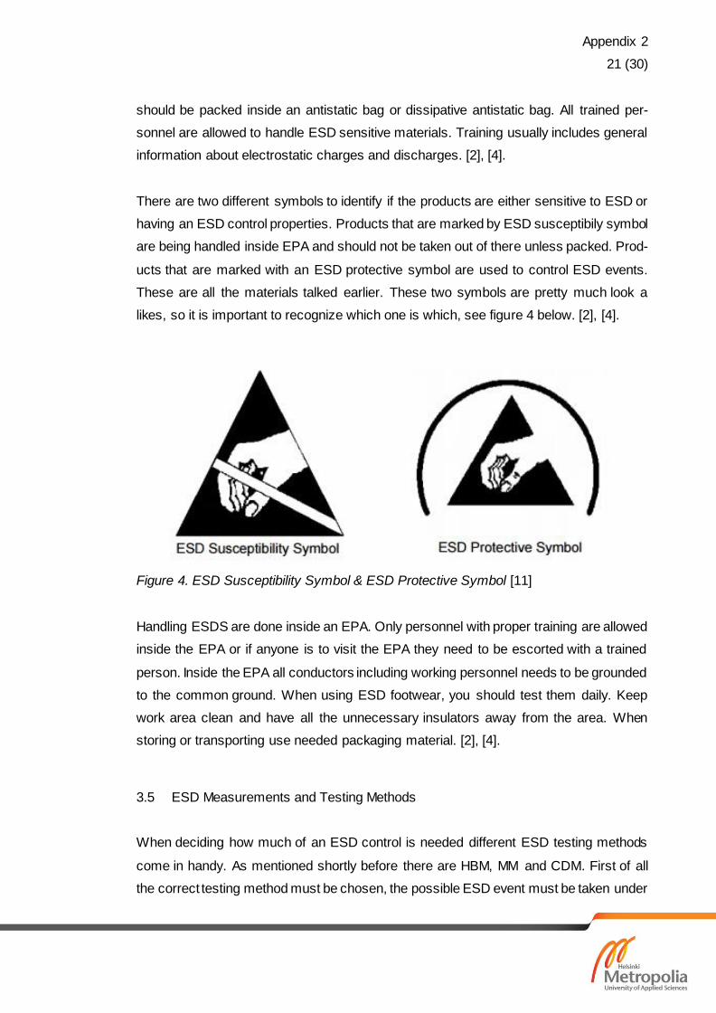
There are two different symbols to identify if the products are either sensitive to ESD or
having an ESD control properties. Products that are marked by ESD susceptibily symbol
are being handled inside EPA and should not be taken out of there unless packed. Prod-
ucts that are marked with an ESD protective symbol are used to control ESD events.
These are all the materials talked earlier. These two symbols are pretty much look a
likes, so it is important to recognize which one is which, see figure 4 below. [2], [4].
Figure 4. ESD Susceptibility Symbol & ESD Protective Symbol [11]
Handling ESDS are done inside an EPA. Only personnel with proper training are allowed
inside the EPA or if anyone is to visit the EPA they need to be escorted with a trained
person. Inside the EPA all conductors including working personnel needs to be grounded
to the common ground. When using ESD footwear, you should test them daily. Keep
work area clean and have all the unnecessary insulators away from the area. When
storing or transporting use needed packaging material. [2], [4].
3.5 ESD Measurements and Testing Methods
When deciding how much of an ESD control is needed different ESD testing methods
come in handy. As mentioned shortly before there are HBM, MM and CDM. First of all
the correct testing method must be chosen, the possible ESD event must be taken under

Appendix 2
22 (30)
consideration. Is it going to be a discharge from a human, an automated machine/tool or
an automated manufacturing line. [2], [4], [5].
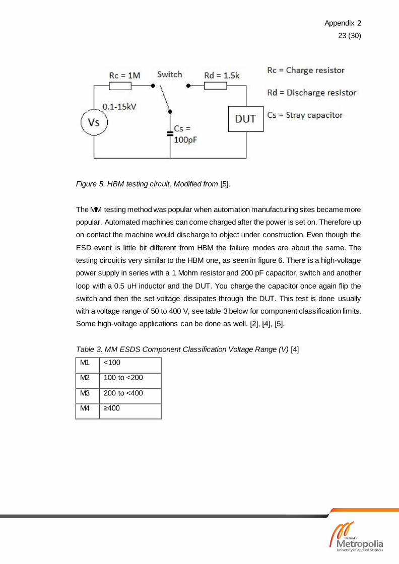
The HBM testing method is the most common one out of these. It simulates an ESD from
a human onto an electronic device. This is the most common case of ESD damage at
electrical repair workshop. Usual damage that this ESD event makes is metal penetra-
tion, junction damage, melting metal layers and gate-oxide damage. The set up for this
testing method is a simple circuit with a high-voltage power supply in series with a 1
Mohm resistor and a 100 pF capacitor, a switch and another loop with a 1.5 kohm resistor
and the device under test (DUT). See figure of the circuit below, figure 5. The testing
circuit works by first having a closed circuit on the power supply side, charging the ca-
pacitor. Once the capacitor is fully charged the switch is used to remove the capacitor
from the power supply and discharging to the other loop. The charged voltage fully dis-
sipates through the 1.5 kohm resistor and the DUT. The range of voltage values used
varies between 0.1 to 15 kV. The voltage determines what level of susceptibility the DUT
has. Table below shows the classification voltage range, see table 2. [2], [4], [5].
Table 2. HBM ESDS Component Classification Voltage Range (V) [4]
0A < 125
0B 125 to <250
1A 250 to <500
1B 500 to <1000
1C 1000 to <2000
2 2000 to <4000
3A 4000 to <8000
3B ≥8000
Appendix 2
23 (30)
Figure 5. HBM testing circuit. Modified from [5].
The MM testing method was popular when automation manufacturing sites became more
popular. Automated machines can come charged after the power is set on. Therefore up
on contact the machine would discharge to object under construction. Even though the
ESD event is little bit different from HBM the failure modes are about the same. The
testing circuit is very similar to the HBM one, as seen in figure 6. There is a high-voltage
power supply in series with a 1 Mohm resistor and 200 pF capacitor, switch and another
loop with a 0.5 uH inductor and the DUT. You charge the capacitor once again flip the
switch and then the set voltage dissipates through the DUT. This test is done usually
with a voltage range of 50 to 400 V, see table 3 below for component classification limits.
Some high-voltage applications can be done as well. [2], [4], [5].
Table 3. MM ESDS Component Classification Voltage Range (V) [4]
M1 <100
M2 100 to <200
M3 200 to <400
M4 ≥400

Appendix 2
24 (30)
Figure 6. MM testing circuit. Modified from [5].
The CDM testing method is considered useful when using automated manufacturing
lines. The charge will build up to the device and will damage it when discharging into a
grounded conductor. The setup for this testing method is little bit more complex than the
previous two. DUT is placed on a metal ground plate, and these two are separated with
and insulating material, making it act like a capacitor. This way the DUT can charge up.
The metal plate is then connected to a high-voltage power source in series with a larger
than 10 Mohm resistor. You test it by charging the plate with wanted voltage though the
power source and then discharging it. A table of classification voltage limits is described
below, table 4. Also a model of CDM testing circuit below the table, see figure 7. [2], [4],
[5].
Table 4. CDM ESDS Component Classification Voltage Range (V) [4]
C1 <150
C2 150 to <250
C3 250 to <500
C4 500 to <1000
C5 1000 to <1500
C6 1500 to <2000
C7 ≥2000

Appendix 2
25 (30)
Figure 7. CDM testing circuit. [5].
These three testing methods are the most common ones used. They help you to figure
out which type of ESD event you are facing and what level of protection is required. The
limits are not guaranteed, but they give and idea how much the DUT can with stand until
failure. [2], [4], [5].
3.6 ESD Training and Auditing
Every electrical repair workshop needs to give their personnel a proper ESD training. By
this training personnel will know how to work on ESDS. Basic training includes the basic
concept of ESD events, ESD effects on an ESDS, how to handle ESDS, usage of ESD
control garments and equipment, and working methods inside an EPA. This material
covers all of these fields and could be used for training. Importance of training relies
heavily to cut the unnecessary expenses. As mentioned before ESD damage can cut
profitability and reliability. In a constantly developing field such as electronics the com-
petition is tough. If products from one company are not as reliable as in another one,
customers will use the more reliable one. So it is important that whoever is working on
ESDS knows what they are doing. [2], [4].

Appendix 2
26 (30)
After personnel has been trained, occasional audits can be done to proof that the ESD
control does its job and the personnel keep working by the rules. These auditions are
done by checking the working areas, condition and proper usage of ESD control equip-
ment and garment, there are no unnecessary insulators inside an EPA, ESDS are
packed and labelled correctly, discharge devices are wired to the ground, ESD protective
floor is clean, intact and connected to the common ground, EPA is marked properly and
there are no unauthorized personnel there, and that the ESD maintenance schedule is
maintained. These audits are also made when a new repair workshop is opened or when
making a contract with a new customer. In that case the audit is held by the customer’s
representative and escorted inside the workshop with authorized personnel. [4].
4 EPA
ESD protected area is where all the ESDS are being worked on. This area is essential
for ESD safe environment. EPA can be a simple workstation with an ESD safe desk,
tools, and ESD control equipment. When setting up an EPA there is no idea going all in
ESD control. By recognizing how much of ESD control is needed, a significant amount
of money can be saved. Main feature of an EPA is an environment where ESD events
should not occur and in case of an ESD event it will safely dissipate without doing any
damage to sensitive devices. [4].
4.1 Setting up an EPA
When setting up an EPA everything that were discussed in Chapter 3. ESD protection,
can be implemented. First of all flooring options need to be considered. Choosing the
correct flooring option for your need is important, are heavy objects going to be moved
across the floor or is a cheap PVC vinyl going to be enough. After building the floor you
start by defining what areas are going to be EPA and which are not. All areas that are
used to work on ESDS should be marked with EPA signs and floor tape to show the
boundaries for authorized and unauthorized personnel. Inside EPA there should not be
any materials that work as an insulator. Insulators increase chance for an ESD event to
occur. For visitors, outside an EPA should be disposable ESD heel grounders and a test
unit to check that your shoes are conducting. At the workstation there should be an ESD
Appendix 2
27 (30)
safe workbench that is connected to the common ground via 1 Mohm resistor. ESD wrist
bands are recommended, but not always needed. With a proper flooring option and con-
ductive shoes, human body will not charge high enough to do damage. There are excep-
tions depending on the level of ESD control. Workstation includes ESD safe chair, work-
bench, tools and containers. If ESDS are being transported outside of EPA or stored, the
packing material is necessary. Packing material is also stored inside EPA. Trolley’s that
are used to move ESDS inside EPA needs to be ESD safe as well. Storage area and
storage selves need to made ESD safe. EPA is necessary to keep clean and mainte-
nance regularly. Impurities on surfaces can carry a lethal charge for an ESDS. For clean-
ing use only cleaning supplies that are meant for ESD materials. Personnel working in-
side an EPA are equipped with proper ESD control garments. [4].
4.2 Temporary EPA
When working out in the field, setting up a temporary EPA is usually needed. Equip-
ment’s to build a simple yet effective EPA can be carried along. ESD mat, conductive
shoes or heel grounders, wrist band that can be connected to the mat and proper tools
are needed. Up on arrival to worksite, define the perimeters for needed space and close
to the device you are working on. All unnecessary movement and transportation is clever
to cut out and minimize the risk of an ESD event. Lay down the ESD mat and connect
your wristband to it. Now you and the ESD mat share the same potential. Make sure that
the ESD mat is intact to ensure it works properly. On this mat it is safe work on ESDS.
Just make sure you are standing on the mat and not on the floor, it might not be dissipa-
tive. After repair work is done, move the repaired device back to its place with caution to
prevent any damage. [2], [4].
5 Discussion
What can be learned about ESD safety through this thesis, is that there are a lot of dif-
ferent ways to prevent ESD events from occurring. Controlling ESD is also really im-
portant for companies to make their product lines and repairs as profitable as possible.
ESD control is a huge market with a lot of unnecessary and necessary stuff. Without a
general knowledge on ESD, companies can overextend their safety to way beyond and
spend significant amounts of money for basically nothing. Doing the research can take

Appendix 2
28 (30)
a while but will cut the budget for you. Static electricity is a common phenomenon that
happens constantly around us. A discharge from a tip of your finger that you cannot
notice can damage a sensitive component so that it will be either broken or defected,
and break down prematurely. There are definitely people doing research to improve the
testing methods and how to spot the currently unnoticeable defects. And as the technol-
ogy advances, integrated circuits are getting smaller and more complex causes them to
be more sensitive for external factors such as ESD. While technology improves, the ma-
terials used or circuits that are made should be done less susceptible to these external
factors. But in overall ESD control is used widely in all different field and it is good to
know how easily static electricity builds up and what the discharge can do.
6 Conclusion
ESD is a common problem in the field of technology and the main goal of this thesis was
to find out how to protect from ESD events. The way to approach these problems were
doing research on different sources. Going through different material online and as books
gave better idea on the whole subject. Due to the amount of problems that a simple ESD
shock can do, ESD safety and control is important. There are several different ways to
control ESD, not every single one of them needs to be used. It is important to recognize
what level of ESD control is needed. Workstation also known as EPA needs to be clean
and there should not be any materials that are insulative. Dissipative and conductive
materials provide a safe way for the accumulated charge to be transferred away. Insula-
tors does not dissipate and can carry a charge that will harm your ESDS. Basically with
a proper dissipative floor, conductive ESD shoes and training, you can limit almost all
damage occurred from a human body. The goal was reached by finding out enough
information for how to work with ESDS and proper instructions were made.
Appendix 2
29 (30)
References
[1] Wikipedia. 2017. Electrostatic discharge. [ONLINE] Available at: https://en.wikipe-
dia.org/wiki/Electrostatic_discharge [Accessed 13 May 2017].
[2] ESD suojaus/Toni Viheriäkoski. 2010. Staattinen sähkö ja ESD. [ONLINE] Available
at: https://esdsuojaus.net/toni-viheriakoski/. [Accessed 12 May 2017].
[3] Wikipedia. 2017. Static electricity. [ONLINE] Available at: https://en.wikipe-
dia.org/wiki/Static_electricity [Accessed 15 March 2017].
[4] EOS/ESD Association. 2013. ESD Association. [ONLINE] Available at: https://www.esda.org/ [Accessed 13 May 2017].
[5] Planet Analog. 2006. EDN network. [ONLINE] Available at: http://www.edn.com/de-
sign/test-and-measurement/4368466/Understanding-and-comparing-the-differences-in-
ESD-testing [Accessed 2 May 2017].
[6] Staticworx. 2009. ESD knowledge center. [ONLINE] Available at: https://www.stat-
icworx.com/articles [Accessed 5 May 2017].
[7] Armeka Engineering. 2009. Armeka Engineering. [ONLINE] Available at:
http://www.armekaengineering.com/esd/tuotteet [Accessed 5 May 2017].
[8] Electronic Design/Sanjay Agarwal. 2014. Understanding ESD and EOS Failures in
Semiconductor Devices. [ONLINE] Available at: http://www.elec-
tronicdesign.com/power/understanding-esd-and-eos-failures-semiconductor-devices.
[Accessed 8 May 2017].

Appendix 2
30 (30)
[9] Mini-Circuits. 2015. The Prevention and Control of Electrostatic Discharge (ESD)
(AN-40-005). [ONLINE] Available at: https://www.minicircuits.com/app/AN40-005.pdf.
[Accessed 26 March 2017].
[10] All About Circuits. 2015. Electrostatic Discharge. [ONLINE] Available at:
https://www.allaboutcircuits.com/textbook/semiconductors/chpt-9/electrostatic-dis-
charge/. [Accessed 22 March 2017].
[11] ESD Systems. 2015. ESD Awareness Symbols. [ONLINE] Available at:
http://esdsystems.descoindustries.com/ESD-Symbols.aspx. [Accessed 10 May 2017].
[12] Google Image Search. 2015. Triboelectric series. [ONLINE] Available at: http://pubs.rsc.org/services/images/RSCpubs.ePlatform.Service.FreeContent.Image-Service.svc/ImageService/Articleimage/2016/CS/c5cs00812c/c5cs00812c-f18_hi-res.gif. [Accessed 17 March 2017]. [13] WEIDINGER. 2015. EPA sign. [ONLINE] Available at: https://www.weidinger.eu/en/shop/esd_protection/esd_equipment_for_work-space/equipment/warning_signs/wl20397. [Accessed 17 March 2017]. [14] Somerset Solders. 2017. ESD Wrist Strap and Footwear Test Station. [ONLINE] Available at: http://www.somersetsolders.com/esd-wrist-strap-and-footwear-test-sta-tion/p306. [Accessed 3 May 2017].