embedded electronic systems driven by run-time ...
264
Francisco Fons Lluís EMBEDDED ELECTRONIC SYSTEMS DRIVEN BY RUN-TIME RECONFIGURABLE HARDWARE DOCTORAL THESIS Supervised by Dr. Enrique F. Cantó Navarro Departament d’Enginyeria Electrònica, Elèctrica i Automàtica Tarragona 2012 UNIVERSITAT ROVIRA I VIRGILI EMBEDDED ELECTRONIC SYSTEMS DRIVEN BY RUN-TIME RECONFIGURABLE HARDWARE Francisco Fons Lluís DL: T. 877-2012
-
Upload
khangminh22 -
Category
Documents
-
view
0 -
download
0
Transcript of embedded electronic systems driven by run-time ...
Francisco Fons Lluís
EMBEDDED ELECTRONIC SYSTEMS DRIVEN BY RUN-TIME RECONFIGURABLE HARDWARE
DOCTORAL THESIS
Supervised by Dr. Enrique F. Cantó Navarro
Departament d’Enginyeria Electrònica, Elèctrica i Automàtica
Tarragona
2012
UNIVERSITAT ROVIRA I VIRGILI EMBEDDED ELECTRONIC SYSTEMS DRIVEN BY RUN-TIME RECONFIGURABLE HARDWARE Francisco Fons Lluís DL: T. 877-2012

UNIVERSITAT ROVIRA I VIRGILI EMBEDDED ELECTRONIC SYSTEMS DRIVEN BY RUN-TIME RECONFIGURABLE HARDWARE Francisco Fons Lluís DL: T. 877-2012
ESCOLA TÈCNICA SUPERIOR D’ENGINYERIA DEPARTAMENT D’ENGINYERIA ELECTRÒNICA, ELÈCTRICA I AUTOMÀTICA Avinguda dels Països Catalans, 26 Campus Sescelades 43007 Tarragona – SPAIN Tel. + 34 977 559 610 Fax + 34 977 559 605 e-mail: [email protected] http://sauron.etse.urv.es/DEEEA/
Enrique F. Cantó Navarro, professor at the Department of Electronic, Electrical and Automatic Control Engineering of the University Rovira i Virgili, STATES: That the present thesis, entitled “Embedded electronic systems driven y run-time reconfigurable hardware”, presented by Francisco Fons Lluís for the award of the degree of Doctor, has been carried out under my supervision at the Department of Electronic, Electrical and Automatic Control Engineering of the University Rovira i Virgili. Tarragona, March 2012 Doctoral Thesis Supervisor Dr. Enrique F. Cantó Navarro
UNIVERSITAT ROVIRA I VIRGILI EMBEDDED ELECTRONIC SYSTEMS DRIVEN BY RUN-TIME RECONFIGURABLE HARDWARE Francisco Fons Lluís DL: T. 877-2012

UNIVERSITAT ROVIRA I VIRGILI EMBEDDED ELECTRONIC SYSTEMS DRIVEN BY RUN-TIME RECONFIGURABLE HARDWARE Francisco Fons Lluís DL: T. 877-2012
v
Abstract Run-time reconfigurable hardware technology has experienced a big progress in the last decade after both academia and industry research communities have jointly got involved in this issue, bringing the necessary talent and energy to definitively put this technology to the service of the society. Many indicators confirm today that dynamic partial reconfiguration is no longer just for the avid early explorers of the recent past: improved programmable logic devices supporting this technology have been shipped; a valid method and design flow supported by acceptable EDA tools has been established; potential use cases and killer applications that can benefit from this technology have been identified; and last but not least, the first commercial products/systems driven by this technology are already being launched to the market. This PhD dissertation addresses the exploration of run-time reconfigurable hardware to implement embedded applications, exploiting its inherent strengths in flexibility and adaptability, as well as in power and system cost savings. This work does research on the conception of an open system architecture driven by a reconfiguration engine suitable for synthesizing flexible embedded electronic systems on SRAM-based FPGA/SoC devices. Thereby, it pays attention to the identification, from an application-driven viewpoint, of computational tasks typically synthesized in static hardware –e.g. general-purpose processors (MCU, DSP, GPU) or programmable logic (FPGA, SoC)– in which dynamic partial reconfiguration can be used to advantage. Several application fields like control engineering (e.g. PID and fuzzy logic controllers), digital computing (e.g. trigonometrics, 2D convolution), or full complex electronic systems (e.g. biometric recognition system, automotive electronic control unit) have been investigated from an algorithmic standpoint first and prototyped then through commercial devices –e.g., Xilinx, Atmel and Altera platforms– provided with on-the-fly reconfiguration, pioneering the use of run-time reconfigurable hardware by first time in the scientific literature in some of them. This work demonstrates that a complete run-time reconfigurable computing ecosystem provided with a high enough level of maturity for its exploitation in the industry is today already in place, making feasible –although further advances are still required, especially regarding automatic tools– the professional design and development of embedded electronic systems. Thus, in a future of digital system design increasingly parallel and programmable, many application opportunities for run-time reconfigurable hardware abound. In this sense, the future of this computing paradigm is highly promising, hoping that the intellectual effort invested in this area by the research community, the FPGA vendors and the industry in general helps to enhance the life quality of the human beings in the near future. The work conducted in this PhD dissertation aims at contributing to this goal.
UNIVERSITAT ROVIRA I VIRGILI EMBEDDED ELECTRONIC SYSTEMS DRIVEN BY RUN-TIME RECONFIGURABLE HARDWARE Francisco Fons Lluís DL: T. 877-2012

vi
UNIVERSITAT ROVIRA I VIRGILI EMBEDDED ELECTRONIC SYSTEMS DRIVEN BY RUN-TIME RECONFIGURABLE HARDWARE Francisco Fons Lluís DL: T. 877-2012
vii
Acronyms and abbreviations AFAS Automatic Fingerprint Authentication System AHB Advanced High-performance Bus ALU Arithmetic Logic Unit AMBA Advanced Microcontroller Bus Architecture ASIC Application Specific Integrated Circuit ASIL Automotive Safety Integrity Level ASIP Application-Specific Instruction-set Processor ASSP Application Specific Standard Product API Application Programming Interface ARM Advanced RISC Machine AXI Advanced Extensible Interface BOM Bill Of Materials CAD Computer Aided Design CAGR Compound Annual Growth Rate CAN Controller Area Network CISC Complex Instruction Set Computing CLB Configurable Logic Block CORDIC COordinate Rotation DIgital Computer CPLD Complex Programmable Logic Device CPU Central Processing Unit CUDA Compute Unified Device Architecture DDR-SDRAM Doble Data Rate Synchronous Dynamic Random Access Memory DMA Direct Memory Access DPRAM Dual Port Random Access Memory DRAM Dynamic Random Access Memory D&D Design and Development ECU Electronic Control Unit EDA Electronic Design Automation E/E Electrical/Electronic EPP Extensible Processing Platform ESA European Space Agency FLC Fuzzy Logic Controller FPGA Field Programmable Gate Array FPSLIC Field Programmable System Level Integrated Circuit FPU Floating Point Unit FSM Finite State Machine GPGPU General-Purpose computation on Graphics Processing Unit GPP General-Purpose Processor GPS Global Positioning System GPU Graphics Processing Unit HDL Hardware Description Language HLS High-Level Synthesis HPC High-Performance Computing HPRC High-Performance Reconfigurable Computing ICAP Internal Configuration Access Port ICT Information & Communication Technology IEC International Electrotechnical Commission I/O Input/Output IP Intellectual Property ISA Instruction Set Architecture ISO International Organization for Standardization
UNIVERSITAT ROVIRA I VIRGILI EMBEDDED ELECTRONIC SYSTEMS DRIVEN BY RUN-TIME RECONFIGURABLE HARDWARE Francisco Fons Lluís DL: T. 877-2012

viii
JTAG Joint Test Action Group LCD Liquid Crystal Display LUT Look-Up Table MAC Multiplier-Accumulator MCU Microcontroller Unit MCyT Spanish Ministry of Science and Technology MMU Memory Management Unit MPMC Multi-Port Memory Controller NASA National Aeronautics and Space Administration NoC Network-on-Chip NPI Native Port Interface NRE Non-Recurring Engineering NVM Non-Volatile Memory OEM Original Equipment Manufacturer OS Operating System OTP One-Time Programmable PAL Programmable Array Logic PC Personal Computer PCB Printed Circuit Board PID Proportional Integral Derivative PIN Personal Identification Number PLA Programmable Logic Arrays PLB Peripheral Local Bus PLD Programmable Logic Device PR Partial Reconfiguration PROM Programmable Read-Only Memory PRM Partially Reconfigurable Module PRR Partially Reconfigurable Region PSoC Programmable System-on-Chip RAM Random Access Memory RC Reconfigurable Computing RISC Reduced Instruction Set Computing ROM Read Only Memory RTL Register Transfer Level SDRAM Synchronous Dynamic Random Access Memory SEU Single Event Upset SME Small and Medium Enterprises SoC System-on-Chip SoPC System-on-Programmable-Chip SRAM Static Random Access Memory SWaP Size, Weight and Power UART Universal Asynchronous Receiver Transmitter VHDL Very High Speed Integrated Circuit Hardware Description Language VLIW Very Long Instruction Word V&V Verification and Validation XCL Xilinx CacheLink
UNIVERSITAT ROVIRA I VIRGILI EMBEDDED ELECTRONIC SYSTEMS DRIVEN BY RUN-TIME RECONFIGURABLE HARDWARE Francisco Fons Lluís DL: T. 877-2012

ix
List of figures Figure 1.1 Milestones of the roadmap towards run-time reconfigurable computing Figure 1.2 Use of FPGA devices Figure 1.3 Recent achievements in run-time reconfigurable computing Figure 1.4 DES horizontal (design technology) and vertical (embedded apps)
disciplines Figure 2.1 Antifuse programming technology Figure 2.2 SRAM programming technology Figure 2.3 MRAM programming technology Figure 2.4 SRAM-based FPGA conceptual view Figure 2.5 SRAM-based FPGA logic cell Figure 4.1 Embedded system components breakdown into host CPU,
reconfiguration engine, external memory and I/O Figure 4.2 High level model of the FPGA embedded system split in physical devices Figure 4.3 Dynamic partial self-reconfigurable FPGA high level model Figure 4.4 Minimalist system architecture based on one PR partition and one
repository Figure 4.5 Embedded system architecture based on two PR partitions and one
repository Figure 4.6 Embedded system architecture composed of two PR partitions and two
sytem repositories which split the reconfiguration data from the application data
Figure 4.7 VAPRES system architecture Figure 4.8 Autovision system architecture Figure 4.9 KIT-ITIV system architecture Figure 4.10 ESM system architecture Figure 4.11 Molen system architecture Figure 5.1 Self-reconfigurable FPGA versus externally-reconfigurable FPGA Figure 5.2 Internal FPGA configuration port in Atmel AT94K FPSLIC Figure 5.3 Altera Excalibur EPXA reconfiguration controller architecture Figure 5.4 Arbitration of configuration interfaces in Xilinx FPGAs Figure 5.5 Xilinx FPGA reconfiguration controller architecture Figure 5.6 Decoupling of bitstream provider and consumer via a simple dual-port
FIFO Figure 5.7 Block diagram of the system architecture deployed in the ML401
platform Figure 5.8 PR design flow (EDA tools, source code files and resultant bitstreams) Figure 7.1 Block diagram of a closed-loop control system based on a PID controller Figure 7.2 AT40K logic cell based on two 3-input LUTs and one 1-bit flip-flop Figure 7.3 AT94K series architecture Figure 7.4 Scheduling of the PID algoritm performed with a multiplier and an adder Figure 7.5 Block diagram of the PID coprocessor implemented in the FPGA Figure 7.6 Reconfigurable operands selector Figure 7.7 PID coprocessor Figure 7.8 AT94K prototype board developed Figure 7.9 Floorplanning, placement and routing of the PID app in the AT94K40
FPSLIC Figure 7.10 Reconfigurable selector of the operands of the multiplier and the adder Figure 8.1 Fuzzy-based control system constituted by two inputs and one output Figure 8.2 Three-stage fuzzy process Figure 8.3 Fuzzy control surface z=f(x,y) obtained in the fuzzification, rule inference
and defuzzification stages. Segmentation and indexing of the surface
UNIVERSITAT ROVIRA I VIRGILI EMBEDDED ELECTRONIC SYSTEMS DRIVEN BY RUN-TIME RECONFIGURABLE HARDWARE Francisco Fons Lluís DL: T. 877-2012
x
Figure 8.4 Block diagram of the AT94K40-based FLC Figure 8.5 Block diagram of the FLC embedded in the AT94K40 FPSLIC Figure 8.6 Scheduling of the fuzzy computing Figure 8.7 DR-MIXER and DR-ROM modules Figure 8.8 Automatic testing of the FLC design Figure 8.9 Floorplanning of the fuzzy logic controller in the AT94K40 FPSLIC Figure 9.1 ML401 evaluation board used in the prototyping of the 2D convolver Figure 9.2 System architecture and functional components breakdown Figure 9.3 2D convolution split in four stacked functional blocks Figure 9.4 Parallelism and 4-stage pipeline of the 2D convolver placed in the PRR Figure 9.5 Isotropic filter Kj,i of kernel 13x13 with 28 common taps coefficients Figure 9.6 Example of image 2D convolution based on an isotropic filter of kernel
13x13 with processing of 4 pixels in parallel into the PRR Figure 9.7 Partial bitstreams of image processors based on different 2D convolution
features. FPGA floorplanning and partitioning into static and PR regions Figure 9.8 Composition of the full bitstream placed in the FPGA at a given time split
in the static region and the 2D convolver located in the PRR Figure 10.1 Circular CORDIC rotation of a vector in a 2D coordinate system Figure 10.2 Block diagram of the AT94K40-based trigonometric CORDIC coprocessor Figure 10.3 Internal structure of the CORDIC coprocessor Figure 10.4 Multiplexing of KCORDIC by dynamic partial reconfiguration Figure 10.5 Sign controller: static version versus dynamic version Figure 10.6 Static 3x1-multiplexer versus dynamic 3x1-multiplexer Figure 10.7 Floorplanning of the trigonometric CORDIC computer in the AT94K40
FPSLIC Figure 11.1 Design flow of the embedded AFAS application Figure 11.2 Image processing tasks breakdown of the AFAS algorithm Figure 11.3 Fingerprint image processing stages Figure 11.4 Sequential execution flow (temporal partitioning) distributed in static-
and PR-regions (spatial partitioning) Figure 11.5 AFAS development platform Figure 11.6 System architecture of the reconfigurable fingerprint recognition
processor Figure 11.7 Biometric recognition system architecture in a Virtex-4 FPGA Figure 11.8 Spatial partitioning and floorplanning of the AFAS in one static region
and one reconfigurable region of the FPGA. Temporal partitioning of the application in sequential stages performed in the reconfigurable region
Figure 12.1 AUTOSAR layer-based model Figure 12.2 Porting of the AUTOSAR ECU architecture to a SoC/FPGA platform Figure 12.3 Block diagram of an automotive ECU deployed in programmable logic Figure 12.4 HW/SW co-design of a safety architecture that isolates the safety-
relevant ports from non-safety ports to guarantee the freedom from interference
UNIVERSITAT ROVIRA I VIRGILI EMBEDDED ELECTRONIC SYSTEMS DRIVEN BY RUN-TIME RECONFIGURABLE HARDWARE Francisco Fons Lluís DL: T. 877-2012
xi
List of tables and code Table 1.1 Scientific conferences focused on reconfigurable hardware technology Table 1.2 International journals which broach reconfigurable hardware as topic of
interest Table 3.1 Research projects oriented to run-time reconfigurable hardware
technology Table 3.2 Patents based on reconfigurable hardware technology Table 3.3 Reconfigurable computing research groups Table 3.4 PhD dissertations related to reconfigurable computing Table 5.1 Atmel AT94K/AT94S FPSLIC reconfiguration controller Table 5.2 Altera Excalibur EPXA reconfiguration controller Table 5.3 Partial Reconfiguration features of Xilinx FPGAs Table 5.4 Reconfiguration controllers implemented on Spartan-3 and Virtex-II Pro
devices Table 5.5 Reconfiguration controllers implemented on Virtex-4/-5 and Spartan-6
devices Table 5.6 Reconfiguration features of the next generation Xilinx and Altera devices Table 7.1 PID computation in different HW/SW platforms Table 7.2 Hardware resources used in the PID controller implementation Table 8.1 Hardware resources used in the fuzzy logic controller implementation Table 8.2 Time breakdown of the FLC tasks Table 9.1 FPGA spatial partitioning Table 9.2 Processing time of the different tasks Table 9.3 Use of FPGA hardware resources Table 9.4 Hardware implementation features Table 10.1 Numerical representation of the CORDIC corrective constants K32 Table 10.2 Comparison of different HW/SW implementations of the CORDIC
algorithm Table 10.3 Time breakdown of the execution tasks Table 10.4 Computation error Table 10.5 Hardware resources used in the CORDIC computer implementation Table 10.6 Hardware resources used in the CORDIC atan(y/x) computer
implementation Table 11.1 Processing time breakdown of the different tasks executed in different
AFAS platforms. Tasks performance comparison: (i) SW-only approach on a personal computer platform based on an Intel Core 2 Duo processor @ 1.83GHz, (ii) HW/SW co-design on an Altera Excalibur EPXA10 SoPC based on an ARM9 processor @ 200MHz and custom hardware coprocessors @ 24MHz/48MHz, and (iii) PR-HW/SW co-design on a Xilinx Virtex-4 XC4VLX25 FPGA based on a Microblaze processor @ 100MHz and custom reconfigurable hardware coprocessors @ 50MHz/100MHz
Table 11.2 Balance of resources in the AFAS application based on Virtex-4 FPGA Table 14.1 Development platforms used in the different research works Table 14.2 European and Spanish research projects framework of this PhD
dissertation Code 5.1 Reconfiguration of an 8-bit resource of the FPGA via the MCU software
code Code 5.2 Reconfiguration of the FPGA via the MCU software code Code 5.3 Reconfiguration function used by the host processor Code 7.1 PID algorithm
UNIVERSITAT ROVIRA I VIRGILI EMBEDDED ELECTRONIC SYSTEMS DRIVEN BY RUN-TIME RECONFIGURABLE HARDWARE Francisco Fons Lluís DL: T. 877-2012
xii
Code 7.2 PID software function prototypes Code 7.3 Reconfiguration of the logic cell’s XLUT and YLUT in each PID cycle Code 8.1 Binary search algorithm based on a 256-sectors surface Code 9.1 Pseudo code of a 13x13 isotropic filter 2D convolution implemented in
SW Code 10.1 Prototypes of the trigonometric functions
UNIVERSITAT ROVIRA I VIRGILI EMBEDDED ELECTRONIC SYSTEMS DRIVEN BY RUN-TIME RECONFIGURABLE HARDWARE Francisco Fons Lluís DL: T. 877-2012
xiii
List of publications Journals
• E. Cantó, M. Fons, F. Fons, M. López, R. Ramos, Fast self-reconfigurable embedded system on Spartan-3, Journal of Universal Computer Science (under 2nd review). • F. Fons, M. Fons, E. Cantó, M. López, Deployment of run-time reconfigurable hardware coprocessors into compute-intensive embedded applications, Journal of Signal Processing Systems, vol. 66, no. 2, pp. 191-221, Springer, 2012. • M. Fons, F. Fons, E. Cantó, M. López, FPGA-based personal authentication using fingerprints, Journal of Signal Processing Systems, vol. 66, no. 2, pp. 153-189, Springer, 2012. • F. Fons, M. Fons, E. Cantó, M. López, Real-time embedded systems powered by FPGA dynamic partial self-reconfiguration: A case study oriented to biometric recognition applications, Journal of Real-Time Image Processing, pp. 1-23, Springer, doi:10.1007/s11554-010-0186-1, 2011. • M. Fons, F. Fons, E. Cantó, Biometrics-based consumer applications driven by reconfigurable hardware architectures, Future Generation Computer Systems, vol. 28, no. 1, pp. 268-286, Elsevier, January 2012. • F. Fons, M. Fons, E. Cantó, Run-time self-reconfigurable 2D convolver for adaptive image processing, Microelectronics Journal, vol. 42, no. 1, pp. 204–217, Elsevier, January 2011. • M. Fons, F. Fons, E. Cantó, Fingerprint Image Processing Acceleration Through Run-Time Reconfigurable Hardware, IEEE Transactions on Circuits and Systems II: Express Briefs, vol. 57, no. 12, pp. 991-995, December 2010. • F. Fons, M. Fons, E. Cantó, System-on-chip design of a Fuzzy Logic controller based on dynamically reconfigurable hardware, International Transactions on Systems Science and Applications, vol. 2, no. 2, pp. 191-196, Xiaglow Research, ISSN 1751-1461, 2006. • F. Fons, M. Fons, E. Cantó, M. López, Trigonometric computing embedded in a dynamically reconfigurable CORDIC system-on-chip, K. Bertels, J.M.P. Cardoso, S. Vassiliadis (Eds.), Reconfigurable Computing: Architectures and Applications, Lecture Notes in Computer Science, vol. 3985, pp. 122-127, Springer, ISBN 978-3-540-36708-6, 2006. • E. Cantó, N. Canyellas, M. Fons, F. Fons, M. López, FPGA Implementation of the ridge line following fingerprint algorithm, J. Becker, M. Platzner, S. Vernalde (Eds.), Field-Programmable Logic and Applications, Lecture Notes in Computer Science, vol. 3203, pp. 1087-1089, Springer, ISBN 3-540-22989-2, 2004.
Book chapters
• M. Fons, F. Fons, Exploiting run-time reconfigurable hardware in the development of automatic fingerprint-based personal recognition applications, Recent Application in Biometrics, pp. 239-266, InTech, ISBN 978-953-307-488-7, July 2011.
UNIVERSITAT ROVIRA I VIRGILI EMBEDDED ELECTRONIC SYSTEMS DRIVEN BY RUN-TIME RECONFIGURABLE HARDWARE Francisco Fons Lluís DL: T. 877-2012
xiv
Internaltional conferences
• E. Cantó, F. Fons, M. López, Self-reconfigurable embedded systems on Spartan-3, International Conference on Field Programmable Logic and Applications, FPL Conference Proceedings, pp. 571-574, Heidelberg, Germany, September 2008. • E. Cantó, M. López, F. Fons, Self-reconfiguration of embedded systems mapped on Spartan-3, International Workshop on Reconfigurable Communication-centric System-on-Chips, ReCoSoC Conference Proceedings, pp. 117-124, Barcelona, Spain, July 2008. • F. Fons, M. Fons, E. Cantó, Approaching fingerprint image enhancement through reconfigurable hardware accelerators, IEEE International Symposium on Intelligent Signal Processing, WISP Conference Proceedings, pp. 457-462, Alcalá de Henares, Spain, October 2007. • M. Fons, F. Fons, E. Cantó, Embedded VLSI accelerators for fingerprint signal processing, IEEE International Symposium on Intelligent Signal Processing, WISP Conference Proceedings, pp. 463-468, Alcalá de Henares, Spain, October 2007. • M. Fons, F. Fons, E. Cantó, M. López, Design of a hardware accelerator for fingerprint alignment, IEEE International Conference on Field Programmable Logic and Applications, FPL Conference Proceedings, pp. 485-488, Amsterdam, The Netherlands, August 2007. • F. Fons, M. Fons, E. Cantó, M. López, Flexible hardware for fingerprint image processing, IEEE International Conference on Ph.D. Research in Microelectronics and Electronics, RME Conference Proceedings, pp. 169-172, Bordeaux, France, July 2007. • M. Fons, F. Fons, E. Cantó, Embedded security: New trends in personal recognition systems, IEEE International Conference on Ph.D. Research in Microelectronics and Electronics, RME Conference Proceedings, pp. 89-92, Bordeaux, France, July 2007. • M. Fons, F. Fons, E. Cantó, Hardware-Software codesign of a fingerprint alignment processor, IEEE International Conference on Mixed Design of Integrated Circuits and Systems, MIXDES Conference Proceedings, pp. 661-666, Ciechocinek, Poland, June 2007. • F. Fons, M. Fons, E. Cantó, Hardware-Software co-design of a dynamically reconfigurable FPGA-based Fuzzy Logic controller, IEEE International Conference on Electronics, Circuits and Systems, ICECS Conference Proceedings, pp. 1228-1231, Nice, France, December 2006. • E. Cantó, F. Fons, M. López, Reconfigurable OPB coprocessors for a Microblaze self-reconfigurable SOC mapped on Spartan-3 FPGAs, IEEE Industrial Electronics Society Conference, IECON Conf. Proceedings, pp. 4940-4944, Paris, France, November 2006. • F. Fons, M. Fons, E. Cantó, System-on-chip design of a Fuzzy Logic controller based on dynamically reconfigurable hardware, International Conference on Self-Organization and Autonomic Systems in Computing and Communications (SOAS), Erfurt, Germany, September 2006. • E. Cantó, M. López, F. Fons, J. del Río, A. Manuel, Automated design flow for multi-context FPGAs, IEEE International Midwest Symposium on Circuits and Systems, MWSCAS Conference Proceedings, pp. 470-474, San Juan, Puerto Rico, USA, August 2006.
UNIVERSITAT ROVIRA I VIRGILI EMBEDDED ELECTRONIC SYSTEMS DRIVEN BY RUN-TIME RECONFIGURABLE HARDWARE Francisco Fons Lluís DL: T. 877-2012
xv
• M. Fons, F. Fons, E. Cantó, Design of an embedded fingerprint matcher system, IEEE International Symposium on Consumer Electronics, ISCE Conference Proceedings, pp. 610-615, Saint Petersburg, Russia, June 2006. • M. Fons, F. Fons, E. Cantó, Design of FPGA-based hardware accelerators for on-line fingerprint matcher systems, IEEE International Conference on Ph.D. Research in MicroElectronics and Electronics, RME Conference Proceedings, pp. 333-336, Otranto, Lecce, Italy, June 2006. • M. Fons, F. Fons, E. Cantó, M. López, Hardware-Software co-design of a fingerprint matcher on card, IEEE International Conference on Electro/Information Technology, EIT Conference Proceedings, East Lansing, Michigan, USA, May 2006. • F. Fons, M. Fons, E. Cantó, Custom-made design of a digital PID control system, IEEE International Conference on Acoustics, Speech, and Signal Processing, ICASSP Proceedings, vol. 3, pp. 1020-1023, Toulouse, France, May 2006. • F. Fons, M. Fons, E. Cantó, M. López, Dynamically reconfigurable CORDIC coprocessor for trigonometric computing, W. Karl, J. Becker, K.E. Groβpietsch, C. Hochberger, E. Maehle (Eds.), International Conference on Architecture of Computing Systems (ARCS), Workshop Proceedings, Lecture Notes in Informatics (LNI), vol. P-81, pp. 254-263, GI-Edition, ISBN 3-88579-175-7, Frankfurt am Main, Germany, March 2006. • M. Fons, F. Fons, N. Canyellas, E. Cantó, M. López, Hardware-Software co-design of an automatic fingerprint acquisition system, IEEE International Symposium on Industrial Electronics, ISIE Conference Proceedings, pp. 1123-1128, Dubrovnik, Croatia, June 2005. • E. Cantó, N. Canyellas, M. López, M. Fons, F. Fons, Coprocessor of the ridge line following fingerprint algorithm, Conference on Design of Circuits and Integrated Systems, DCIS Conference Proceedings, pp. 139-143, Bordeaux, France, November 2004. • F. Fons, M. Fons, S. Ibáñez, Biometrics is the key, 24. Tagung Elektronik im Kraftfahrzeug – Neue Technologien, Integration und Systementwurf. Haus der Technik e. V., Essen, Germany, June 2004.
National conferences
• E. Cantó, M. López, F. Fons, R. Ramos, Sistema embebido de rápida auto-reconfiguración sobre Spartan-3, IX Jornadas de Computación Reconfigurable y Aplicaciones, Actas Congreso JCRA, pp. 183-192, Alcalá de Henares, Spain, September 2009. • F. Fons, M. Fons, E. Cantó, M. López, Procesador hardware auto-reconfigurable de Huella Dactilar, VII Jornadas de Computación Reconfigurable y Aplicaciones, Actas Congreso JCRA, pp. 19-26, Zaragoza, Spain, September 2007. • M. Fons, F. Fons, E. Cantó, M. López, Procesador de alineamiento de huellas dactilares, VII Jornadas de Computación Reconfigurable y Aplicaciones, Actas Congreso JCRA, pp. 27-34, Zaragoza, Spain, September 2007. • E. Cantó, M. López, N. Canyellas, M.D. Palomera, M. Fons, F. Fons, Coprocesador para la esqueletización de huellas dactilares, V Jornadas de Computación Reconfigurable y Aplicaciones, Actas Congreso JCRA, pp. 103-108, Sevilla, Spain, September 2005.
UNIVERSITAT ROVIRA I VIRGILI EMBEDDED ELECTRONIC SYSTEMS DRIVEN BY RUN-TIME RECONFIGURABLE HARDWARE Francisco Fons Lluís DL: T. 877-2012
xvi
• M. López, E. Cantó, N. Canyellas, M.D. Palomera, M. Fons, F. Fons, Diseño de un coprocesador hardware para segmentación de huellas dactilares, V Jornadas de Computación Reconfigurable y Aplicaciones, Actas Congreso JCRA, pp. 173-178, Sevilla, Spain, September 2005. • E. Cantó, N. Canyellas, M. Fons, F. Fons, M. López, Coprocesador de extracción de minutia para MicroBlaze, IV Jornadas de Computación Reconfigurable y Aplicaciones, Actas Congreso JCRA, pp. 605-611, Barcelona, Spain, September 2004. • F. Fons, M. Fons, N. Canyellas, M. López, E. Cantó, Planteamiento de una alternativa de solución al reto del proceso de matching sobre bases de datos grandes. Aplicación del método en los sistemas de identificación personal basados en biometría de huella dactilar, III Jornadas de Computación Reconfigurable y Aplicaciones (JCRA), E. Boemo Scalvinoni, F. Gómez Arribas, S. López Buedo, G. Sutter Capristo (Eds.), Computación Reconfigurable & FPGAs, pp. 597-610, Madrid, Spain, September 2003. • M. Fons, F. Fons, N. Canyellas, M. López, E. Cantó, Codiseño hardware-software de un algoritmo de matching biométrico, III Jornadas de Computación Reconfigurable y Aplicaciones (JCRA), E. Boemo Scalvinoni, F. Gómez Arribas, S. López Buedo, G. Sutter Capristo (Eds.), Computación Reconfigurable & FPGAs, pp. 399-406, Madrid, Spain, September 2003. • F. Fons, M. Fons, N. Canyellas, M. López, E. Cantó, Trusted smart cards: a future new generation of embedded systems that merges biometrics and system-on-chip technology, Ph.D. Student Meeting on Electronics Engineering, Departament d’Enginyeria Electrònica, Elèctrica i Automàtica, Universitat Rovira i Virgili, Tarragona, Spain, July 2003. • M. Fons, F. Fons, N. Canyellas, M. López, E. Cantó, Trends on personal recognition systems: Evolving to biometric security, Ph.D. Student Meeting on Electronics Engineering, Departament d’Enginyeria Electrònica, Elèctrica i Automàtica, Universitat Rovira i Virgili, Tarragona, Spain, July 2003.
Others
• F. Fons, M. Fons, FPGA-based automotive ECU design addresses AUTOSAR and ISO 26262 standards, Xcell Journal, issue 78, pp. 20-31, Xilinx, First Quarter 2012. • F. Fons, M. Fons, Auf die finger blicken, Elektronik Journal, pp. 16-18, October 2010. • F. Fons, M. Fons, Making biometrics the killer app of FPGA dynamic partial reconfiguration, Xcell Journal, issue 72, pp. 24-31, Xilinx, Third Quarter 2010. • F. Fons, M. Fons, E. Cantó, M. López, Dynamically reconfigurable CORDIC coprocessor for trigonometric computing, Mitteilungen – Gesellschaft für Informatik (GI) e. V., Parallel-Algorithmen und Rechnerstrukturen, no. 23, pp. 34-43, ISSN 0177-0454, December 2006. • M. López, E. Cantó, M. Palomera, F. Fons, M. Fons, N. Canyellas, Hardware-Software co-design for fingerprint biometric identification, Instrumentation Viewpoint, SARTI Technological Development Centre of Remote Acquisition and Data Processing Systems, pp. 7-10, ISSN 1697-2562, Spring 2005.
UNIVERSITAT ROVIRA I VIRGILI EMBEDDED ELECTRONIC SYSTEMS DRIVEN BY RUN-TIME RECONFIGURABLE HARDWARE Francisco Fons Lluís DL: T. 877-2012
xvii
Content Abstract …………………………………….………………………………………………………. v
Acronyms and abbreviations ………………………….……………………………………… vii
List of figures ………………………….………………………………………………………….. ix
List of tables and code ………………………….………………………………………………. xi
List of publications ………………………….………………………………………………….. xiii
Journals .......................................................................................................... xiii Book chapters ................................................................................................. xiii International conferences ................................................................................ xiv National conferences ....................................................................................... xv Others ............................................................................................................. xvi
Content …………………………………………………….……………………………………….. xvii
PART I. OUTLINE ……………………………………………….……………………………….. 1
1. Reconfigurable computing …………………………………….…………..……………… 3
1.1 Introduction ……………………………………………………………………………………. 3 1.1.1 History: roadmap towards reconfigurable computing ……………………………… 4 1.1.2 The present of reconfigurable hardware technology ………………………….……. 8 1.2 Motivation ………………………………………………………………………………………. 9 1.2.1 Scientific events and specialized journals ……………………………………………. 11 1.3 Dissertation aims and scope ……………………………………………………………….. 13 1.3.1 Contribution and thesis organization …………………………………………………. 15 References …………………………………………………………………………………………… 18
PART II. STATE OF THE ART ……………….………………………………………..……… 19
2. Embedded systems and reconfigurable hardware ……………………….............. 21
2.1 Embedded electronic systems ……………………………………………………………... 21 2.1.1 Implementation alternatives …………………………………………………………….. 21 2.2 Field programmable gate arrays ………………………………………………………….. 23 2.2.1 Programming technology …………………………………………………………………. 24
- Antifuse ……………………………………………………………………………………. 24 - EPROM, EEPROM and Flash ………………………………………………………… 25 - SRAM ………………………………………………………………………………………. 25 - MRAM ……………………………………………………………………………………… 26
2.3 SRAM-based reconfigurable hardware technology ………………………………....... 26 2.3.1 Reconfiguration model ……………………………………………………………………. 29
- Single context ……………………………………………………………………………. 29 - Partially reconfigurable ………………………………………………………………… 29 - Multi-context …………………………………………………………………………….. 30
2.3.2 Granularity ………………………………………………………………………………….. 30 - Fine-grain architecture ………………………………………………………………... 31 - Coarse-grain architecture …………………………………………………………….. 31 - Hybrid architecture …………………………………………………………………….. 31
UNIVERSITAT ROVIRA I VIRGILI EMBEDDED ELECTRONIC SYSTEMS DRIVEN BY RUN-TIME RECONFIGURABLE HARDWARE Francisco Fons Lluís DL: T. 877-2012
xviii
2.3.3 Reconfigurability features ………………………………………………………………… 31 - Device activity during reconfiguration …………………………………………….. 31 - Amount of device resources reconfigured …………………………………………. 32 - Bitstream format and downloading mechanism …………………………………. 33 - Link between bitstream repository and reconfiguration engine ……………… 33 - Reconfiguration engine interface ……………………………………………………. 34 - Reconfiguration latency ……………………………………………………………….. 35
2.4 Bitstream manipulation and configuration techniques ……………………………… 36 2.4.1 Bitstream compression/decompression ………………………………………………. 36 2.4.2 Bitstream relocation ………………………………………………………………………. 37 2.4.3 Bitstream security …………………………………………………………………………. 38 2.4.4 Configuration bootstrapping and multiple-boot ……………………………………. 38 2.4.5 Configuration overclocking ………………………………………………………………. 39 2.4.6 Configuration caching ……………………………………………………………………. 39 2.4.7 Configuration prefetching ………………………………………………………………... 40 2.4.8 Configuration scrubbing …………………………………………………………………. 40 2.4.9 Configuration scheduling ………………………………………………………………… 40 2.4.10 Online bitstream build ………………………………………………………………….. 41 2.4.11 Low power consumption target ……………………………………………………….. 41 2.5 Summary ……………………………………………………………………………………….. 42 References …………………………………………………………………………………………… 43 3. Research and deployment ……………………………………..………………………….. 45
3.1 Related academic and industrial advances …………………………………………….. 45 3.1.1 Research projects ………………………………………………………………………….. 45
- RECONF 2 ………………………………………………………………………………… 45 - ADRIATIC ………...……................................................................................ 46 - AMDREL …………………………………………………………………………………… 46 - MORPHEUS ………………………………………………………………………………. 46 - 4S …………………………………………………………………………………………… 46 - ANDRES …………………………………………………………………………………… 47 - AETHER …………………………………………………………………………………… 47 - RECOPS …………………………………………………………………………………… 47 - HARTES …………………………………………………………………………………… 48 - CRISP ………………………………………………………………………………………. 48 - ERA …………………………………………………………………………………………. 48 - REFLECT ………………………………………………………………………………….. 48
3.1.2 Patents ……………………………………………………………………………………….. 49 3.1.3 Research groups ……………………………………………………………………………. 50 3.1.4 PhD dissertations ………………………………………………………………………….. 52 3.2 Reconfigurable hardware devices …………………………………………………………. 53 3.2.1 Commercial and industrial FPGAs and SoCs ……………………………………….. 53
- Altera ………………………………………………………………………………………. 53 - Atmel ………………………………………………………………………………………. 53 - Lattice ……………………………………………………………………………………… 54 - Xilinx ………………………………………………………………………………………. 54 - Others ……………………………………………………………………………………... 55
3.2.2 Research and academic reconfigurable platforms …………………………………. 57 - POEtic ……………………………………………………………………………………… 57 - Chimaera …………………………………………………………………………………. 58 - ADRES …………………………………………………………………………………….. 58 - DISC ………………………………………………………………………………………… 59 - DPGA ………………………………………………………………………………………. 59 - Time-multiplexed FPGA ……………………………………………………………….. 59
UNIVERSITAT ROVIRA I VIRGILI EMBEDDED ELECTRONIC SYSTEMS DRIVEN BY RUN-TIME RECONFIGURABLE HARDWARE Francisco Fons Lluís DL: T. 877-2012
xix
- Garp ……………………………………………………………………………………….. 60 - PipeRench ………………………………………………………………………………… 60 - PRISM ……………………………………………………………………………………… 61 - Others ……………………………………………………………………………………… 61
3.3 Summary ……………………………………………………………………………………….. 61 References …………………………………………………………………………………………… 62
PART III. DESIGN AND DEVELOPMENT …………………………….…………………….. 63
4. Run-time reconfigurable system architecture …………….…………..……………. 65
4.1 Standardized flexible hardware/software architecture …..…………………………. 65 4.2 High level functional blocks ……………………………….………………………………. 66 4.2.1 Host CPU ………………………………………………………….………………………….. 67 4.2.2 External memory …………………………………………………………………………… 68 4.2.3 Input/Output ……………………………………………………………………………….. 68 4.2.4 Reconfiguration engine …………………………………………………………………… 68 4.3 System components breakdown ………………………………………………………….. 69 4.3.1 Standard static design ……………………………………………………………………. 70 4.3.2 Dynamic partial self-reconfiguration design ………………………………………… 71 4.4 System modeling and deployment ………………………………………………………... 71 4.4.1 Minimalist model: single data repository and single PR partition ………………. 72 4.4.2 Model with single data repository and two PR partitions …………………………. 75 4.4.3 Model with two data repositories and two PR partitions ………………………….. 77 4.4.4 Comparison with other state-of-the-art architectures …………………………….. 78
- VAPRES …………………………………………………………………………………… 78 - Autovision ………………………………………………………………………………… 79 - KIT-ITIV ……………………………………………………………………………………. 80 - ESM ………………………………………………………………………………………… 81 - Molen …………………………………………………………………………................ 82
4.5 Summary ……………………………………………………………………………………….. 83 References …………………………………………………………………………………………… 84 5. Reconfiguration engine ………………………………….…………………………………. 85
5.1 Reconfiguration design parameters ……………………………………………………… 85 5.2 State-of-the-art reconfiguration controllers: a survey ……………………………….. 86 5.2.1 Closed reconfiguration controller solutions ………………………………………….. 88
- Atmel AT94K/AT94S FPSLIC …………………………………………………………. 88 - Altera Excalibur EPXA SoPC …………………………………………………………. 90
5.2.2 Open reconfiguration controller solutions …………………………………………… 93 - Xilinx Virtex/Spartan FPGAs ………………………………………………………… 93 - Research on reconfiguration controllers based on Xilinx FPGAs …………….. 95
5.3 Reconfiguration engine architecture and modelling ………………………………….. 97 5.3.1 Reconfiguration controller architecture ………………………………………………. 97 5.3.2 Analytical model formulation ……………………………………………………………. 99
- Minimum reconfiguration time ……………………………………………………… 99 - Reconfiguration process scheduled in a cyclic task …………………………….. 101
5.3.3 System integration and proof of feasibility …………………………………………… 102 - Performance evaluation ……………………………………………………………….. 107
5.3.4 Comparison with state-of-the-art architectures ……………………………………. 109 5.3.5 Next generation reconfiguration engines ……………………………………………... 112 5.4 Summary ……………………………………………………………………………………….. 113 References …………………………………………………………………………………………… 113
UNIVERSITAT ROVIRA I VIRGILI EMBEDDED ELECTRONIC SYSTEMS DRIVEN BY RUN-TIME RECONFIGURABLE HARDWARE Francisco Fons Lluís DL: T. 877-2012
xx
PART IV. PROOFS OF CONCEPT AND USE CASES ………………….………………… 115
6. Exploration and exploitation ……………………….……………………………………. 117
6.1 Potential applications ……………………………………………………………………….. 117 6.1.1 Space applications ………………………………………………………………………… 117 6.1.2 Bio-inspired applications ………………………………………………………………… 118 6.1.3 Data security applications ……………………………………………………………….. 119 6.1.4 Thermal self-protected systems ………………………………………………………… 120 6.1.5 Software defined radio …………………………………………………………………….. 121 6.1.6 Control applications ……………………………………………………………………….. 122 6.1.7 Hardware emulation and rapid prototyping …………………………………………. 123 6.1.8 Digital signal processing and arithmetic computing ………………………………. 124 6.1.9 Image processing and multimedia applications …………………………………….. 124 6.1.10 Telecommunications and networking ……………………………………………….. 125 6.1.11 Automotive applications ………………………………………………………………… 127 6.1.12 High-performance computing …………………………………………………………. 127 6.2 Success cases of commercial products and industrial applications ……………… 128 6.2.1 Consumer electronics …………………………………………………………………….. 128 6.2.2 Computing platforms ……………………………………………………………………… 128 6.2.3 NASA/ESA aerospace missions ………………………………………………………… 129 6.2.4 Signal processing at CERN ………………………………………………………………. 129 6.2.5 Software defined radio …………………………………………………………………….. 129 6.2.6 Cryptography ………………………………………………………………………………… 130 6.3 Summary ……………………………………………………………………………………….. 130 References …………………………………………………………………………………………… 130 7. PID controller …………………………………………………………….…………………… 133
7.1 Introduction ……………………………………………………………………………………. 133 7.1.1 PID algorithm ……………………………………………………………………………….. 134 7.2 Related work …………………………………………………………………………………… 135 7.3 Implementation ……………………………………………………………………………….. 137 7.3.1 Atmel AT94K field programmable system level integrated circuit ………………. 137 7.3.2 HW/SW co-design and run-time reconfiguration …………………………………… 139 7.3.3 System prototyping ………………………………………………………………………… 142 7.3.4 Experimental results ……………………………………………………………………… 145 7.4 Summary ……………………………………………………………………………………….. 146 References …………………………………………………………………………………………… 146 8. Fuzzy logic controller ………………………………………………………………………. 147
8.1 Introduction …………………………………………………………………………………… 147 8.1.1 Fuzzy logic fundamentals ………………………………………………………………… 148 8.2 Related work …………………………………………………………………………………… 149 8.3 Hardware/Software co-design …………………………………………………………….. 152 8.3.1 Fuzzy algorithm …………………………………………………………………………….. 152 8.3.2 System architecture ……………………………………………………………………….. 154 8.3.3 FPGA dynamic partial reconfiguration ………………………………………………… 156 8.4 Performance evaluation ……………………………………………………………………... 157 8.5 Summary ……………………………………………………………………………………….. 159 References …………………………………………………………………………………………… 159 9. 2D convolution processor ……………………………………….………………………… 161
9.1 Introduction ……………………………………………………………………………………. 161
UNIVERSITAT ROVIRA I VIRGILI EMBEDDED ELECTRONIC SYSTEMS DRIVEN BY RUN-TIME RECONFIGURABLE HARDWARE Francisco Fons Lluís DL: T. 877-2012

xxi
9.2 Related work …………………………………………………………………………………… 162 9.3 FPGA-based design …………………………………………………………………………… 163 9.3.1 System architecture ……………………………………………………………………….. 164 9.3.2 Adaptive 2D convolver …………………………………………………………………….. 166 9.4 Experimental results ….……………………………………………………………………… 169 9.4.1 Virtex-4 FPGA ……………………………………………………………………………….. 169 9.4.2 Performance evaluation …………………………………………………………………… 169 9.5 Summary ……………………………………………………………………………………….. 175 References …………………………………………………………………………………………… 176 10. Trigonometric CORDIC computer ……………………………………………………... 177
10.1 Introduction ................................................................................................... 177 10.1.1 CORDIC algorithm applied to trigonometrics ............................................... 178 10.2 Related work .................................................................................................. 180 10.3 Run-time reconfigurable hardware implementation ......................................... 181 10.3.1 Hardware/Software co-design and run-time reconfiguration ........................ 182 10.4 Unified fine-grain reconfigurable implementation …………………………………… 182 10.4.1 Coprocessor architecture ............................................................................. 183 10.4.2 Performance evaluation ............................................................................... 187 10.5 Specific coarse-grain reconfigurable implementation ………………………………. 188 10.5.1 Coprocessor architecture ............................................................................ 188 10.5.2 Performance evaluation ............................................................................... 189 10.6 Summary ....................................................................................................... 189 References ............................................................................................................. 190 11. Automatic fingerprint authentication system ........................................... 191
11.1 Introduction ................................................................................................... 191 11.1.1 Basics of biometrics ..................................................................................... 192 11.1.2 Automatic fingerprint authentication system ............................................... 194 11.2 Related work .................................................................................................. 194 11.3 Design and development ................................................................................ 195 11.3.1 Batch process of mutually exclusive tasks ................................................... 197 11.3.2 Spatial and temporal partitioning of tasks ................................................... 201 11.4 Experimental results ...................................................................................... 201 11.4.1 Approach I: Full FPGA reconfiguration on Excalibur SoPC …………………….. 202 11.4.2 Approach II: Partial FPGA reconfiguration on Virtex-4 …………………………... 204 11.4.3 Performance evaluation …………………………………………………………………. 207 11.5 Summary ....................................................................................................... 210 References .............................................................................................................. 212 12. Automotive electronic control unit ........................................................... 213
12.1 Introduction ................................................................................................... 213 12.1.1 AUTOSAR .................................................................................................... 214 12.1.2 ISO 26262 ................................................................................................... 214 12.2 Related work .................................................................................................. 215 12.3 System architecture ........................................................................................ 217 12.3.1 Real scenario ............................................................................................... 217 12.3.2 ECU deployment on FPGA-based static hardware ........................................ 219 12.3.3 ECU deployment on run-time reconfigurable hardware ................................ 223 12.4 Summary ....................................................................................................... 223 References ............................................................................................................. 224
UNIVERSITAT ROVIRA I VIRGILI EMBEDDED ELECTRONIC SYSTEMS DRIVEN BY RUN-TIME RECONFIGURABLE HARDWARE Francisco Fons Lluís DL: T. 877-2012
xxii
PART V. CONCLUSIONS .................................................................................. 225
13. Reconfigurable hardware technology today: strengths and weaknesses ...... 227
13.1 Benefits of run-time reconfigurable hardware ................................................. 227 13.1.1 FPGA technology ......................................................................................... 227 13.1.2 Time-to-solution and life cycle ..................................................................... 228 13.1.3 Portability and immunity against components obsolescence ........................ 228 13.1.4 System versatility, adaptability and self-adaptibity ...................................... 229 13.1.5 Early system validation ............................................................................... 229 13.1.6 Performance improvement, acceleration and parallelism .............................. 229 13.1.7 Hardware customisation .............................................................................. 230 13.1.8 Hardware reuse and functional density ........................................................ 230 13.1.9 Reduction of complexity, space, weight and cost .......................................... 230 13.1.10 Power consumption ................................................................................... 231 13.1.11 System survivability and self-healing ......................................................... 231 13.1.12 Rapid prototyping platform but also end-user product ............................... 231 13.1.13 Technology accessibility ............................................................................. 232 13.1.14 Host coupling ............................................................................................ 232 13.2 Weak points of reconfigurable hardware technology ........................................ 232 13.2.1 Low ease of use and designer productivity ................................................... 232 13.2.2 Advances in design flow and development tools still needed ......................... 233 13.2.3 Lack of commercial devices with better reconfiguration features ................... 233 13.2.4 Software but also hardware skills needed .................................................... 234 13.2.5 Component cost .......................................................................................... 234 13.2.6 Lack of killer applications in place ............................................................... 234 13.2.7 Energy management is increasingly demanded ............................................ 235 13.2.8 Embedded security aspects ......................................................................... 235 13.3 Summary ....................................................................................................... 235 References ............................................................................................................. 236 14. Conclusions and future work .................................................................... 237
14.1 Conclusions .................................................................................................. 237 14.2 Research projects .......................................................................................... 239 14.2.1 TRUST-eS ................................................................................................... 239 14.2.2 DELFIN ....................................................................................................... 241 14.2.3 PIBES ......................................................................................................... 241 14.3 Future work ................................................................................................... 242
UNIVERSITAT ROVIRA I VIRGILI EMBEDDED ELECTRONIC SYSTEMS DRIVEN BY RUN-TIME RECONFIGURABLE HARDWARE Francisco Fons Lluís DL: T. 877-2012
Part I
Outline
UNIVERSITAT ROVIRA I VIRGILI EMBEDDED ELECTRONIC SYSTEMS DRIVEN BY RUN-TIME RECONFIGURABLE HARDWARE Francisco Fons Lluís DL: T. 877-2012

UNIVERSITAT ROVIRA I VIRGILI EMBEDDED ELECTRONIC SYSTEMS DRIVEN BY RUN-TIME RECONFIGURABLE HARDWARE Francisco Fons Lluís DL: T. 877-2012
3
Chapter 1 Reconfigurable computing Reconfigurable computing (RC) constitutes today a consolidated implementation technique of applications –or functionality in general– synthesizable electronically in distributed look-up tables (LUTs), flip-flops and memory blocks of an SRAM-based field programmable logic device. In essence, it brings a new perspective to the design and development of embedded electronic systems, featuring a strong influence on system-on-chip (SoC) architectures and taking full advantage of the inherent parallelism and adaptability of reconfigurable hardware technology. This chapter briefly introduces reconfigurable computing and outlines the scope and goals of this PhD dissertation, which tackles the exploitation possibilities of run-time reconfigurable hardware in the embedded space. Based on hardware/software codesign and driven by dynamic partial reconfiguration, the reconfigurable computing paradigm enables the partitioning of a computational problem into a batch process of scheduled serial and parallel tasks to be performed sequentially in a set of shared silicon resources, balancing thus key design parameters like area (resources required), time (processing latency involved), functional density and power (both static and dynamic terms) in its implementation.
1.1 Introduction
Very often software and hardware arise as two feasible implementation alternatives of an application through digital electronics, subjected to the paradigms of computation-in-time and computation-in-space, respectively. The decision of mapping a computational task either in hardware or in software depends, in general, on the specific constraints of the application itself. On the one hand, software solutions are based on a general-purpose processor or CPU that handles a set of instructions executed sequentially, giving rise to a procedural implementation or instruction flow. As result, software is flexible since the processing can be changed by only modifying the list of instructions or program code, but also relatively inefficient due to the instruction fetch-decode-execute mechanism limited by the sequential execution – one instruction after the other. On the contrary, hardware designs offer high performance due to their customized problem-focused solution –a specific hardware circuitry is synthesized on silicon, with no extra overhead for solving a more general problem– and their spatially parallelized execution, where each operator exists at a different point in space, although this comes at the cost of involving so many hardware resources as necessary, resulting in a structural implementation or configuration flow [DeHon and Wawrzynek, DAC 1999]. The emergence of run-time reconfigurable hardware technology –materialized through SRAM-based field programmable gate array (FPGA) devices some decades ago– introduces a new methodology to balance space and time in the electronic implementation of applications, decomposing the target application into a series of processing tasks which follow an effective temporal and spatial partitioning. Thus, reconfigurable computing (RC) is defined as the study of computation using reconfigurable hardware devices [Bobda, Springer 2007]. With it, digital hardware design becomes soft and its original structural implementation evolves to a simple structural programming. Some terminology must also be defined to address the concepts of reconfigurability. On the one hand, in computing science the term programmable refers to the time domain. It is a type of flexible computations where a sequence of instructions is loaded and executed in the time dimension by using one or several processing elements. Like this, programming means instruction scheduling and it relates to software flow. On the other hand, the term configurable introduces the space domain. It is a type
UNIVERSITAT ROVIRA I VIRGILI EMBEDDED ELECTRONIC SYSTEMS DRIVEN BY RUN-TIME RECONFIGURABLE HARDWARE Francisco Fons Lluís DL: T. 877-2012
4
of flexible computations where only one or a few instructions per processing element are loaded and the execution is performed in the dimensions of space and time concurrently. Therefore, configuration means the setup of structures and preadjustment of logic blocks and it clearly concerns hardware. Moreover, as a subset of configurable, the term reconfigurable referred to a device means that such device can be configured more than once. Still a deeper term within reconfiguration is dynamic, run-time, on-the-fly or active reconfiguration; while configuration or reconfiguration is usually not feasible during operation, dynamic reconfiguration means that reconfiguration may happen at run-time, i.e. during application execution. Thus, dynamic reconfiguration implies that an active device may be partially reconfigured, while ensuring the correct operation of the rest of active circuits that are not being changed. This is known as partial reconfiguration (PR) and refers to the ability to dynamically modify blocks of a programmable logic device by downloading partial bitstream files while the remaining logic on the device continues to operate without interruption. Finally, the term self-reconfiguration extends the dynamic reconfiguration concept to specialized autonomous devices where specific circuits of the device itself are used to control the reconfiguration of other parts of the device, being the integrity of these control circuits guaranteed during reconfiguration [Zomaya, Springer 2006]. Designers realized soon that the volatility of SRAM-based FPGAs could be exploited to gain a competitive advantage in many applications. Since the configuration of these devices can be changed by a completely electrical process performed by a specific engine, either at run-time or off-line, SRAM-based FPGAs become the workhorse of numerous reconfigurable applications. These devices contain an array of LUTs for synthesizing combinational functions, flip-flops for sequential finite state machines, memory blocks for data storage, DSP blocks for compact signal processing, clock management blocks for configuring system clocks, and interconnection nets to link all these resources giving rise to a made-to-measure computing system. By means of reconfiguration technology, all these resources can be highly customized to the instantaneous needs of an application, where the configurable structures are changed during circuit operation, allowing the computational resources to be reused in time. The main goal behind the temporal and spatial partitioning of reconfigurable logic resources is to achieve the highest efficiency of reconfigurable systems, taking the maximum advantage of parallelism, resource usage and flexibility [Diessel et al., CDT 2000]. This approach is viable when the target application can be decomposed into a set of functions or stages executed sequentially following a batch process, whose simultaneous availability is not required and where each one of such serial stages, in its turn, is decomposed in a subset of tasks running in serial and/or in parallel instatiated on demand in the same set of shared resources. As a result, the functionality demanded by the application can be performed on the minimum number of processing elements possible at expenses of raising at maximum its usage or functional density. Moreover, usually the reconfiguration latency is sufficiently small, typically in the order of a few milliseconds or less, for those functions to be swapped in real-time [Lysaght and Rosenstiel, Springer 2005]. Other derived benefits can be the reduction in power dissipation in comparison to static hardware solutions. Such reduction is made effective in both static (less hardware resources involved) and dynamic (less activity if some reconfigurable portions of the device are replaced by blank bitstreams when they are not in use) terms of power. Following this introduction, a short walk through the history of reconfigurable computing, from its birth until today, is presented in the next sections.
1.1.1 History: roadmap towards reconfigurable computing
The reconfigurable computing concept was introduced in 1960 by Gerald Estrin, a computer scientist at the Universtity of California, Los Angeles. Dr. Estrin and his group at the UCLA did the earliest work on reconfigurable computer architectures, proposing the idea of a fixed plus variable (F+V) computing system in which a fixed processor
UNIVERSITAT ROVIRA I VIRGILI EMBEDDED ELECTRONIC SYSTEMS DRIVEN BY RUN-TIME RECONFIGURABLE HARDWARE Francisco Fons Lluís DL: T. 877-2012
5
abstraction exists side by side with programmable hardware [Estrin, WJCC 1960]. At that time, the fixed part was implemented in a motherboard composed basically of a general-purpose processor whereas the variable part was made upon a set of specific functional units and their wire harness, composing block modules insertable into the motherboard [Estrin and Turn, TEC 1963]. With this architecture, the reconfiguration was exclusively performed by hand –either changing the wiring harness or replacing some basic blocks by new ones– reaching thus a manual modification of the system functionality [Estrin, AHC 2002]. Close to this concept, programmable logic devices (PLDs) such as programmable read-only memories (PROMs), programmable logic arrays (PLAs) and programmable array logic devices (PALs) have been available since the 1960s, the 1970s and the early 1980s, respectively. These three PLD models are composed of an array of AND-gates connected to another array of OR-gates and they are well suited to implement any computation expressed as a sum of products: the external inputs –in both forms, just as they are and negated– are connected to the AND-gates in a first stage; the intermediate results of this stage are connected then to the second stage composed of OR-gates. Depending on the device –PROM, PAL or PLA– model, only OR, only AND, or both AND and OR connections are user programmable, respectively. However, the use of PROMs and PLAs was quite limited mainly due to technological reasons like its relatively slow maximum operating speed, and concerning PALs, although they started to be used as glue logic, suffered from power consumption problems. Apart from all those issues, the main limitation of these three PLDs is found in their low capacity –restricted by the nature of the AND-OR planes– equivalent to a few hundreds of logic gates. Later, complex programmable logic devices (CPLDs) arose for larger logic circuits, consisting of a set of macro cells (typically composed of several PLAs and flip-flops), I/O blocks and an interconnection network. Despite their relative larger capacity (few hundreds thousands of logic gates), CPLDs are still too small for using in reconfigurable computing to implement big circuits and they are basically used only as glue logic. The extension of the gate array technique to post-manufacturing customisation, based on the idea of using arrays of custom logic blocks surrounded by a perimeter of I/O blocks, all of which can be assembled arbitrarily, gives rise to the FPGA concept, a new type of programmable logic architecture introduced by Ross Freeman, one of the founders of Xilinx Inc. in 1984, who promoted the notion that silicon is free, using such slogan to emphasize the idea that it does not matter that making a single logic gate requires as many as 100 transistors, what really matters is the convenience and time-to-market advantages that reconfigurable FPGAs offer, promoting thus end-user flexibility at the expense of more transistors. The first chip of that company consisted of 85000 transistors (no more than one thousand equivalent gates) and was fabricated in a 2-µm process in 1985, reinforcing already at that time two of the key benefits of reconfigurable computing: the computation is spatial (in contrast to the temporal style associated with microprocessors) and the architecture used in the computation is determined at post-fabrication time and can therefore adapt to the characteristics of the executed algorithm [Xilinx Inc., Xcell 2004]. Probably the first interest from an industrial viewpoint for these ideas started at the beginning of the 1990s once FPGA densities broke the 10K logic gate barrier, being the subject of extensive research and experimentation. At that time, the continuous increase in price for ASIC flows combined with the advance in semiconductor manufacturing made FPGAs a more appealing option for an increasing number of applications, to the extent that they started becoming an actual alternative to low volume ASICs production besides its initial use as rapid prototyping platforms. FPGAs were slowly gaining popularity but still they could not be used for all applications since they did not provide enough hardware resources and software tools had not yet reached enough maturity to create optimized designs. It is in the 1990s when the FPGA design space reached a level of maturity that made them the choice of implementation in many fields, experiencing a fast progress from that moment on. FPGAs started at that time to be used in hardware/software co-design platforms, described in hardware description
UNIVERSITAT ROVIRA I VIRGILI EMBEDDED ELECTRONIC SYSTEMS DRIVEN BY RUN-TIME RECONFIGURABLE HARDWARE Francisco Fons Lluís DL: T. 877-2012
6
languages (HDL) like Verilog and VHDL. Until the middle of the 1990s, all the FPGA-based reconfigurable systems were implemented using statically reconfigurable FPGAs that exhibited some restrictions: to configure a new circuit all FPGA operations had to be completely suspended and a full reconfiguration bitstream had to be loaded in order to reconfigure even one cell of the device; moreover, all information stored in internal registers was lost after a reconfiguration, making it impossible to share internal data between two configurations [Sklyarov et al., Euromicro 1998]. These restrictions were overcome by a new type of SRAM-based dynamically reconfigurable FPGAs. These new devices can be partially updated without suspending operations of the parts that do not need to be modified, such as the Xilinx XC6200 family – the first commercially available FPGA designed in 1995 for run-time reconfigurable computing [Hartenstein et al., FPL 1998]. Since then, run-time reconfigurable computing became a subject of intensive research. The concept of virtual hardware –the idea of using a reconfigurable device to implement a number of applications requiring more resources that those currently available– pointed out to the use of temporal partitioning as a way to implement those applications whose area requirements exceed the reconfigurable logic space available, assuming to a certain extend the availability of unlimited hardware resources [Ling and Amano, FCCM 1993]. Thus, after the advance of single context FPGAs, it arises a new trend based on developing multi-context FPGAs [Trimberger, FPGA 1998], leaded by bipartitioning techniques aimed at splitting the static implementation of a circuit in two or more hardware contexts and switching one context to another in some few nanoseconds by means of multiplexed architectures, increasing thus the logic capacity [Hauck and Borriello, CADICS 1997]. Similarly, the increasing amount of logic available in FPGAs, the development of glitchless partial reconfiguration technology and the reduction of the reconfiguration latency allowed extending the concept of virtual hardware to other new FPGAs able to be partially reconfigured, in portions, without the need of replicating their resources in several identical contexts. Thus, the late 1990s opened the door to new FPGA applications, achieving a good level of performance based on exploiting the functional density of their resources. A new trend is observed in which design teams start to use FPGAs in tandem with standard microprocessors as a way to merge both peripheral functions and custom processing. To maximize performance in such applications, designs must tightly couple the FPGA and microprocessor instead of treating each as independent entities. FPGA vendors start to offer various types of processors for their FPGAs just when FPGA transistor counts grew enough to accommodate them. In the late 1990s, FPGA vendors started offering soft-cores (8-bit, 16-bit and then 32-bit processor cores in HDL, or as prerouted netlists like 8051, ARM7, MIPS, LEON, NIOS II, Microblaze, etc) that hardware designers could add into FPGAs with synthesis and place-and-route tools. Later, in the early 2000s, FPGAs achieve the enough density of transistors to implement microprocessors in the silicon itself, as hard-wired cores next to programmable-logic blocks. Implementing cores in the fabric itself saves space on the chip for programmable logic, lowers power and improves overall performance. As examples, Atmel or Altera introduced ARM and AVR hard-core processors in their SoC devices FPSLIC and Excalibur, respectively. Xilinx integrated PowerPC processors in derivatives of its Virtex-4 and Virtex-5 devices. Although the hardware/software co-design flow (hardware/software partitioning, design synthesis, placement, routing, technological mapping, bitstream generation, co-verification) is more complex than the design flow used in a purely-software approach (software edition, compiling and linking), in the 2000s the FPGA flow was fully available for implementing static or off-line reconfigurable designs but not for covering run-time reconfigurable systems. Devices and tools became powerful enough to deal with most static hardware designs. However, the lack of a well-defined and efficient design flow to develop run-time reconfigurable computing together with the lack of efficient reconfiguration features (reconfiguration bandwidtch, grain, etc) for these devices would drastically limit the explosion of this technology to the masses basically for the first 20
UNIVERSITAT ROVIRA I VIRGILI EMBEDDED ELECTRONIC SYSTEMS DRIVEN BY RUN-TIME RECONFIGURABLE HARDWARE Francisco Fons Lluís DL: T. 877-2012
7
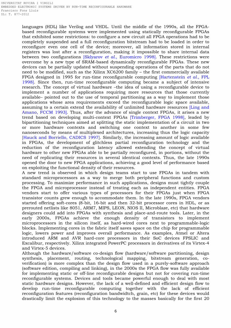
years after the appearance of the first SRAM-based FPGAs. Together with the lack of an appropriate tool set –historically the first stopper of this technology–, the second big stopper of run-time reconfigurable computing at that time was the device cost. FPGAs have historically been restricted to a narrow set of high performance computing applications because of their relative high cost compared with other implementation alternatives (e.g. MCU). However, for over all the quarter of century of life, cost reduction has played a fundamental role in the development of reconfigurable hardware technology. The progress in silicon industry has resulted in a tremendous increase in device capacity of FPGAs while at the same time the cost has decreased drastically. They grow in capacity as they are built by more and more miniaturized cooper process technology, following the Moore’s law which states that the achievable transistor count on a single integrated circuit doubles every 18 to 24 months (130nm, 90nm, 65nm, 40nm, 28nm, etc). This fact lets FPGAs already lodge the whole computation demanded by many applications in one single chip. During the decade of 1990s, there was a reduction of around 10000% in the cost of the basic FPGA building block or logic cell – consisting of one LUT and one flip-flop. Besides, the trends observed in the first decade of 2000s confirmed that advancements in process technology like architectural enhancements, increased logic cell count, and speed contributed to an increase in performance of FPGAs manufactured containing multi-millions of transistors. Thus, in this period of time, the logic compute performance increased approximately by 920% while the logic cell count incremented by 240% and the price per logic cell decreased by 90% [Xilinx Inc., WP375 2010]. From a hardware viewpoint, new nanometer scale fabrication processes allow devices containing several million and ever billion LUTs and flip-flops to be fabricated. An increasing number of logic and I/O resources are available, including complex functional blocks, e.g. on-chip distributed RAM memories, phase-locked loops (PLLs), digital clock managers (DCMs), communication transceivers (GTX, Ethernet, PCIe) and interfaces (DDR-SDRAM), arithmetic circuits (DSP blocks) or cryptographic blocks (e.g. AES core) [Rodriguez-Andina et al., TIE 2007]. Nevertheless, event though partial reconfiguration technology has existed for generations, this feature has only gained big attention recently, becoming a potential implementation alternative of embedded systems based on FPGA devices due basically to the software enhancements of EDA tools carried out in the last years. For this goal, a definitive breakthrough concerning development toolset for run-time reconfigurable computing occurred in 2006. At that time, Xilinx released what probably might be considered the first mature partial reconfiguration design flow provided with automated CAD tools. Such design methodology is built around the PlanAhead tool and definitely makes dynamic reconfiguration feasible, turning it from a heroic activity to a reliable design process. These tools supported Xilinx Virtex-4 FPGAs, which presented further technological enhancements on its architecture oriented to PR like finer reconfiguration granularity and improved reconfiguration bandwidth. Hence, a new era of run-time reconfigurable computing began. An early access version of the PR design tools initially developed by Xilinx was offered to well-qualified partners from both academia and industry who contributed to deploy it and report feedback for its improvement. As one would expect with an early access tool flow, there were opportunities for improvement but the level reached at that moment was conclusive to prove its feasibility aimed at, in the end, porting this design methodology from research to industry. Recently, new tools that allow the FPGA design to become increasingly hardware-independent have been developed (e.g. Simulink model-based design from MathWorks, allowing the use of behavioural descriptions as design entry converted then automatically in HDL code). Summarizing this evolution in only some few milestones, the timeline of Figure 1.1 highlights that reconfigurable computing is a very recent scientific field where, although the concept had its origins 50 years ago, the FPGA technology able to support such paradigm arose 25 years ago and the design flow and tooling for exploiting this technology in a professional way were definitively mature only 5 years ago. Nowadays, with concepts, devices, and professional tools already in place, we live the beginning of a
UNIVERSITAT ROVIRA I VIRGILI EMBEDDED ELECTRONIC SYSTEMS DRIVEN BY RUN-TIME RECONFIGURABLE HARDWARE Francisco Fons Lluís DL: T. 877-2012
8
promising era of computing, with many opportunities ahead that shall let us contribute to the enhancement of our society in aspects like health and quality of life of the citizens.
Figure 1.1 Milestones of the roadmap towards run-time reconfigurable computing
1.1.2 The present of reconfigurable hardware technology
The continuous advances in microelectronics are changing the technology, the computing world and also the society. At a fundamental level, reconfigurable computing is the process of best exploiting the potential of reconfigurable hardware. Just to name some of the most important milestones recently achieved, Xilinx presented in 2010 a new PR design flow, inspired in its previous early access PR modular design flow, based now on partitions. The most relevant highlight of this PR flow –the Xilinx PR fourth generation– is the fact that it is released as mainstream in the design toolset, integrated in the standard tools. This means that PR is officially supported by the FPGA vendor, offered as one more exploitable feature of the device, and therefore accessible from now on by any FPGA development team. Also in 2010, three FPGA vendors announced their next-generation devices featuring, to a greater or lesser extent, dynamic reconfiguration as part of their strategy to take programmable logic forward to higher densities and throughputs. Altera announced its 28-nm Stratix-V FPGA equipped with PR capability as well as the introduction of the PR design flow integrated into its classical Quartus-II tool. In this way, Altera joins for the first time the group of FPGA vendors that provide partial reconfiguration in their devices. Meanwhile, Xilinx announced its next-generation 7-series of FPGAs – its fifth generation of devices that support PR. Finally, also at that time, the startup Tabula Inc. revealed some details of its technology that makes extensive use of dynamic reconfiguration through its multi-context Abax devices. Already in 2011, a new computing wave based on merging hard-core processors with programmable logic in the same fabric arises into the market, promoting the exploitation of system-on-chip solutions. State-of-the-art FPGA devices make possible to implement all the functionality associated to an embedded system in a single chip: one or more hard- or soft-core processors can be placed there along with additional programmable logic to synthesize standard or custom coprocessors. Thus, many platforms tightly integrate today the MCU+FPGA combination and a development tools ecosystem allow an embedded design team to optimally partition their implementation by means of hardware/software co-design. In this direction, Xilinx announced the new generation of the so-called extensible processing platforms (EPP) composed of its Zynq-7000 family of devices. Some months later, Altera announced the new generation of SoC FPGAs Arria-V and Cyclone-V devices. In both –Xilinx and Altera– cases, the devices are composed of a dual-core ARM Cortex-A9 MPCore processor and 28-nm programmable logic. Besides, in the end of 2011, Xilinx started the shipment of the Virtex-7 2000T FPGA device –the world’s highest capacity programmable logic device ever built provided with 6.8 billion transistors on a single chip– and the Zynq-7020 EPP, while Altera released the Arria-V SoC FPGA. Figure 1.2 shows the forecasted change in embedded designs based on FPGA devices which incorporate a hard-wired processor. All these FPGA devices that merge one or more hard core processors with reconfigurable fabric are referred to by the FPGA vendors as programmable system-on-chip (PSoC), system-on-programmable-chip (SoPC),
Xilinx Early Access Partial Reconfiguration Lounge
Modular Design Flow
2006
First Commercial PR-FPGA
Xilinx XC6200
1995
Foundation First FPGA Vendor
Xilinx Inc.
1984
Reconfigurable Computing Concept
G. Estrin
1960
UNIVERSITAT ROVIRA I VIRGILI EMBEDDED ELECTRONIC SYSTEMS DRIVEN BY RUN-TIME RECONFIGURABLE HARDWARE Francisco Fons Lluís DL: T. 877-2012
9
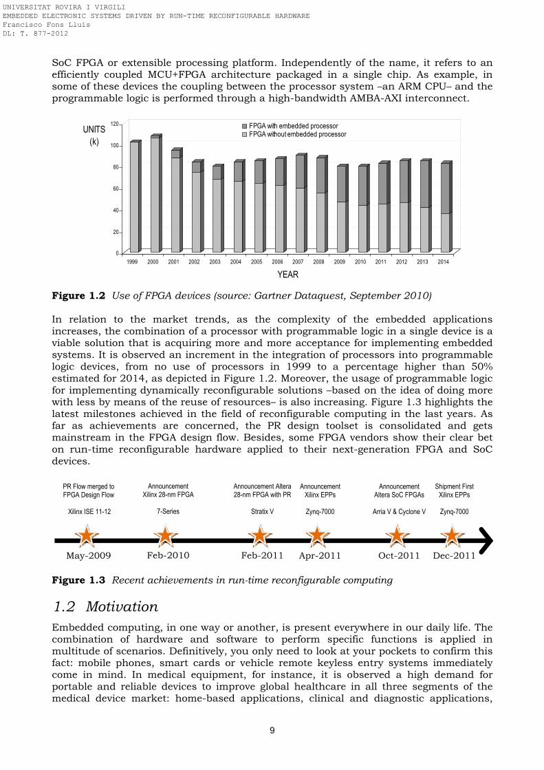
SoC FPGA or extensible processing platform. Independently of the name, it refers to an efficiently coupled MCU+FPGA architecture packaged in a single chip. As example, in some of these devices the coupling between the processor system –an ARM CPU– and the programmable logic is performed through a high-bandwidth AMBA-AXI interconnect.
0
20
40
60
80
100
120UNITS
(k)
1999 2000 2001 2002 2003 2004 2005 2006 2007 2008 2009 2010 2011 2012 2013 2014
YEAR
FPGA with embedded processorFPGA without embedded processor
Figure 1.2 Use of FPGA devices (source: Gartner Dataquest, September 2010) In relation to the market trends, as the complexity of the embedded applications increases, the combination of a processor with programmable logic in a single device is a viable solution that is acquiring more and more acceptance for implementing embedded systems. It is observed an increment in the integration of processors into programmable logic devices, from no use of processors in 1999 to a percentage higher than 50% estimated for 2014, as depicted in Figure 1.2. Moreover, the usage of programmable logic for implementing dynamically reconfigurable solutions –based on the idea of doing more with less by means of the reuse of resources– is also increasing. Figure 1.3 highlights the latest milestones achieved in the field of reconfigurable computing in the last years. As far as achievements are concerned, the PR design toolset is consolidated and gets mainstream in the FPGA design flow. Besides, some FPGA vendors show their clear bet on run-time reconfigurable hardware applied to their next-generation FPGA and SoC devices.
Figure 1.3 Recent achievements in run-time reconfigurable computing
1.2 Motivation
Embedded computing, in one way or another, is present everywhere in our daily life. The combination of hardware and software to perform specific functions is applied in multitude of scenarios. Definitively, you only need to look at your pockets to confirm this fact: mobile phones, smart cards or vehicle remote keyless entry systems immediately come in mind. In medical equipment, for instance, it is observed a high demand for portable and reliable devices to improve global healthcare in all three segments of the medical device market: home-based applications, clinical and diagnostic applications,
Shipment First Xilinx EPPs
Zynq-7000
Dec-2011
Announcement Altera SoC FPGAs
Arria V & Cyclone V
Oct-2011
Announcement Xilinx EPPs
Zynq-7000
Apr-2011
PR Flow merged to FPGA Design Flow
Xilinx ISE 11-12
May-2009
Announcement Xilinx 28-nm FPGA
7-Series
Feb-2010
Announcement Altera 28-nm FPGA with PR
Stratix V
Feb-2011
UNIVERSITAT ROVIRA I VIRGILI EMBEDDED ELECTRONIC SYSTEMS DRIVEN BY RUN-TIME RECONFIGURABLE HARDWARE Francisco Fons Lluís DL: T. 877-2012
10
and medical imaging. In fact, it is said that in the near future about 90% of applications will be embedded systems, most of these mobile appliances that shall be small in size, with very low power consumption and with high performance. Moreover, with the growing popularity of personalized, interactive, real-time technology, it is expected to see in the future a rise in demand for specialized embedded computing systems to support a broad range of new applications – including many that have not yet been envisioned. Due to rapid advancements in integrated circuit technology, the rich theoretical results that have been developed by the research community are now being increasingly applied in practical systems to solve real-world processing problems. Nowadays, an increasing number of researchers believe that the computating challenge for the future is to exploit reconfigurability and parallelism on a single die. The flexibility provided by run-time partial reconfiguration together with the potential for implementing large circuits on limited hardware resources are earned values that make run-time reconfigurable systems an excellent choice for implementing a wide range of low-cost embedded applications. Moreover, reconfigurable hardware technology can clearly contribute to enhance the fault-tolerance capabilities of these systems. Therefore, many applications abound that can take benefit of these technological strengths, delimited by strong constraints on size, weight, cost, and power consumption. For this, it is necessary to define new system architectures based on this new technology able to surpass the performance-cost restrictions of the current solutions in the industry and demonstrate moreover its feasibility. The deployment of this technology involves, in general, to redesign the current solutions from scratch since the requirements inherent to this technology have changed, due especially to the new time-space concept introduced in this approach up to now not present in other technologies like a purely software or static hardware solution based on a Von Neumann or Harvard MCU, DSP, GPU or ASIC. This PhD initiative was born in September 2002 within the context of constituting a new research group inside the Departament d’Enginyeria Electrònica, Elèctrica i Automàtica (DEEEA) of Escola Tècnica Superior d’Enginyeria (ETSE), Universitat Rovira i Virgili (URV), in Tarragona, Spain. The research group is named Development of Embedded Systems (DES) and its topics of interest covers two transverse or horizontal matters aimed at being deployed then into vertical fields. On the one hand, the transverse disciplines focus on the design of embedded system architectures driven by the synthesis of digital circuits. One of the horizontal disciplines deals with the hardware/software co-design of embedded systems on programmable logic. The other discipline focuses on the synthesis of such digital circuits exploiting run-time reconfiguration to reach, in the end, dynamic self-reconfigurable embedded systems. On the other hand, the vertical fields where to deploy these transverse disciplines are organized basically in three main areas: biometrics, cryptography, and a set of more generic computing fields such as arithmetic, digital control and signal/image processing. At that time, the recently founded Development of Embedded Systems research group starts to walk constituted by seven members: three PhD full professors and four PhD students, being the author of this dissertation one member of the last group. The technical profile of all the members met an exciting interest in the design of embedded applications exploiting design techniques based on hardware/software co-design and reconfigurable computing over MCU, FPGA and SoC platforms. Under this scenario, each member takes responsibilities in a specific area so that, when joining all the parts, the group totally covers its global objective: to face up the D&D of embedded systems based on FPGA and SoC devices by exploring efficient system architectures able to lead to significant implementation advances concerning performance and cost. Figure 1.4 shows a snapshot of the different computational application areas of interest of the DES research group, all of them driven by two transverse disciplines. In particular, the author’s research field encompasses the evaluation of run-time reconfigurable hardware as the key technology to address the design of applications portable to embedded electronic systems. As part of this investigation, the author explores how run-time reconfigurable hardware can be used in certain embedded
UNIVERSITAT ROVIRA I VIRGILI EMBEDDED ELECTRONIC SYSTEMS DRIVEN BY RUN-TIME RECONFIGURABLE HARDWARE Francisco Fons Lluís DL: T. 877-2012
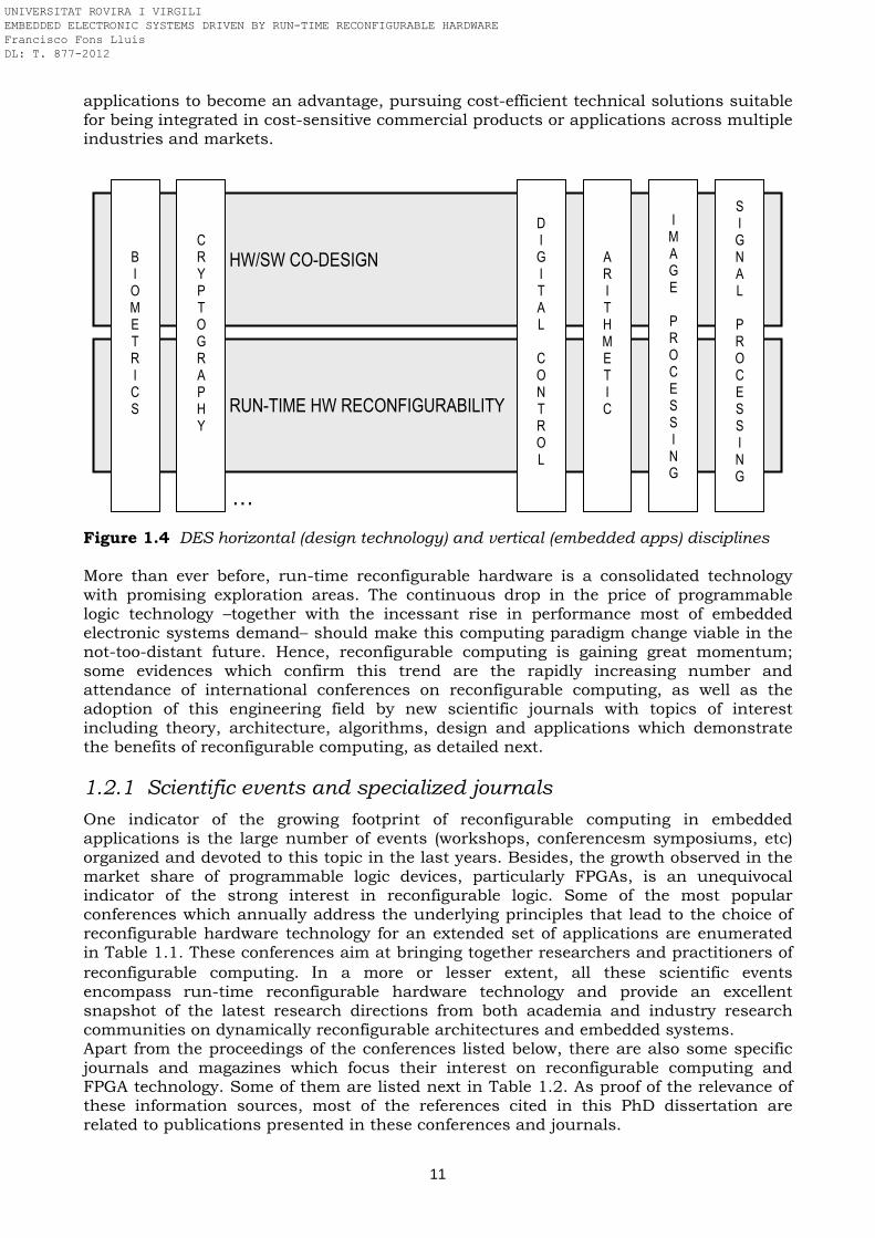
11
applications to become an advantage, pursuing cost-efficient technical solutions suitable for being integrated in cost-sensitive commercial products or applications across multiple industries and markets. Figure 1.4 DES horizontal (design technology) and vertical (embedded apps) disciplines More than ever before, run-time reconfigurable hardware is a consolidated technology with promising exploration areas. The continuous drop in the price of programmable logic technology –together with the incessant rise in performance most of embedded electronic systems demand– should make this computing paradigm change viable in the not-too-distant future. Hence, reconfigurable computing is gaining great momentum; some evidences which confirm this trend are the rapidly increasing number and attendance of international conferences on reconfigurable computing, as well as the adoption of this engineering field by new scientific journals with topics of interest including theory, architecture, algorithms, design and applications which demonstrate the benefits of reconfigurable computing, as detailed next.
1.2.1 Scientific events and specialized journals
One indicator of the growing footprint of reconfigurable computing in embedded applications is the large number of events (workshops, conferencesm symposiums, etc) organized and devoted to this topic in the last years. Besides, the growth observed in the market share of programmable logic devices, particularly FPGAs, is an unequivocal indicator of the strong interest in reconfigurable logic. Some of the most popular conferences which annually address the underlying principles that lead to the choice of reconfigurable hardware technology for an extended set of applications are enumerated in Table 1.1. These conferences aim at bringing together researchers and practitioners of reconfigurable computing. In a more or lesser extent, all these scientific events encompass run-time reconfigurable hardware technology and provide an excellent snapshot of the latest research directions from both academia and industry research communities on dynamically reconfigurable architectures and embedded systems. Apart from the proceedings of the conferences listed below, there are also some specific journals and magazines which focus their interest on reconfigurable computing and FPGA technology. Some of them are listed next in Table 1.2. As proof of the relevance of these information sources, most of the references cited in this PhD dissertation are related to publications presented in these conferences and journals.
…
HW/SW CO-DESIGN
RUN-TIME HW RECONFIGURABILITY
B I O M E T R I C S
C R Y P T O G R A P H Y
D I G I T A L
C O N T R O L
A R I T H M E T I C
I M A G E
P R O C E S S I N G
S I G N A L
P R O C E S S I N G
UNIVERSITAT ROVIRA I VIRGILI EMBEDDED ELECTRONIC SYSTEMS DRIVEN BY RUN-TIME RECONFIGURABLE HARDWARE Francisco Fons Lluís DL: T. 877-2012
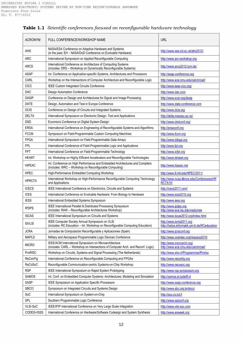
12
Table 1.1 Scientific conferences focused on reconfigurable hardware technology
ACRONYM
FULL CONFERENCE/WORKSHOP NAME
URL
AHS NASA/ESA Conference on Adaptive Hardware and Systems (in the past: EH – NASA/DoD Conference on Evolvable Hardware)
http://www.see.ed.ac.uk/ahs2012/
ARC International Symposium on Applied Reconfigurable Computing http://www.arc-workshop.org
ARCS International Conference on Architecture of Computing Systems (includes: DRS – Workshop on Dynamically Reconfigurable Systems)
http://www.arcs2012.tum.de/
ASAP Int. Conference on Application-specific Systems, Architectures and Processors http://asap-conference.org
CARL Workshop on the Intersections of Computer Architecture and Reconfigurable Logic http://www.ece.cmu.edu/calcm/carl/
CICC IEEE Custom Integrated Circuits Conference http://www.ieee-cicc.org/
DAC Design Automation Conference http://www.dac.com
DASIP Conference on Design and Architectures for Signal and Image Processing http://www.ecsi.org/dasip
DATE Design, Automation and Test in Europe Conference http://www.date-conference.com
DCIS Conference on Design of Circuits and Integrated Systems http://www.dcis.org
DELTA International Symposium on Electronic Design, Test and Applications http://delta.massey.ac.nz/
DSD Euromicro Conference on Digital System Design http://www.dsdconf.org/
ERSA International Conference on Engineering of Reconfigurable Systems and Algorithms http://ersaconf.org
FCCM Symposium on Field-Programmable Custom Computing Machines http://www.fccm.org
FPGA International Symposium on Field-Programmable Gate Arrays http://www.isfpga.org
FPL International Conference of Field-Programmable Logic and Applications http://www.fpl.org
FPT International Conference on Field-Programmable Technology http://www.icfpt.org
HEART Int. Workshop on Highly Efficient Accelerators and Reconfigurable Technologies http://www.isheart.org
HiPEAC Int. Conference on High Performance and Embedded Architectures and Compilers (includes: WRC – Workshop on Reconfigurable Computing)
http://www.hipeac.net
HPEC High-Performance Embedded Computing Workshop http://www.ll.mit.edu/HPEC/2011/
HPRCTA International Workshop on High-Performance Reconfigurable Computing Technology and Applications
http://www.ncsa.illinois.edu/Conferences/HPRCTA10/
ICECS IEEE International Conference on Electronics, Circuits and Systems http://icecs2011.com/
ICES International Conference on Evolvable Hardware: From Biology to Hardware http://www.ices2010.org
IESS International Embedded Systems Symposium http://www.iess.org
IPDPS IEEE International Parallel & Distributed Processing Symposium (includes: RAW – Reconfigurable Architectures Workshop)
http://www.ipdps.org http://www.ece.lsu.edu/vaidy/raw
ISCAS IEEE International Symposium on Circuits and Systems http://www.iscas2012.org/index.html
ISVLSI IEEE Computer Society Annual Symposium on VLSI (includes: RC Education – Int. Workshop on Reconfigurable Computing Education)
http://www.isvlsi2011.org http://helios.informatik.uni-kl.de/RCeducation
JCRA Jornadas de Computación Reconfigurable y Aplicaciones (Spain) http://www.jcraconf.org
MAPLD Military and Aerospace Programmable Logic Devices Conference http://www.cosmiac.org/respace2010
MICRO IEEE/ACM International Symposium on Microarchitecture (includes: CARL – Workshop on Intersections of Computer Arch. and Reconf. Logic)
http://www.microarch.org/ http://www.ece.cmu.edu/calcm/carl/
ProRISC Workshop on Circuits, Systems and Signal Processing (The Netherlands) http://www.stw.nl/Programmas/Prorisc
ReConFig International Conference on Reconfigurable Computing and FPGAs http://www.reconfig.org
ReCoSoC Reconfigurable Communication-centric Systems-on-Chip Workshop http://www.recosoc.org
RSP IEEE International Symposium on Rapid System Prototyping http://www.rsp-symposium.org
SAMOS Int. Conf. on Embedded Computer Systems: Architectures, Modeling and Simulation http://samos.et.tudelft.nl
SASP IEEE Symposium on Application Specific Processors http://www.sasp-conference.org
SBCCI Symposium on Integrated Circuits and Systems Design http://www.sbc.org.br/sbcci
SoC International Symposium on System-on-Chip http://soc.cs.tut.fi
SPL Southern Programmable Logic Conference http://www.splconf.org
VLSI-SoC IEEE/IFIP International Conference on Very Large Scale Integration http://www.vlsi-soc.com
CODES+ISSS International Conference on Hardware/Software Codesign and System Synthesis http://www.esweek.org
UNIVERSITAT ROVIRA I VIRGILI EMBEDDED ELECTRONIC SYSTEMS DRIVEN BY RUN-TIME RECONFIGURABLE HARDWARE Francisco Fons Lluís DL: T. 877-2012
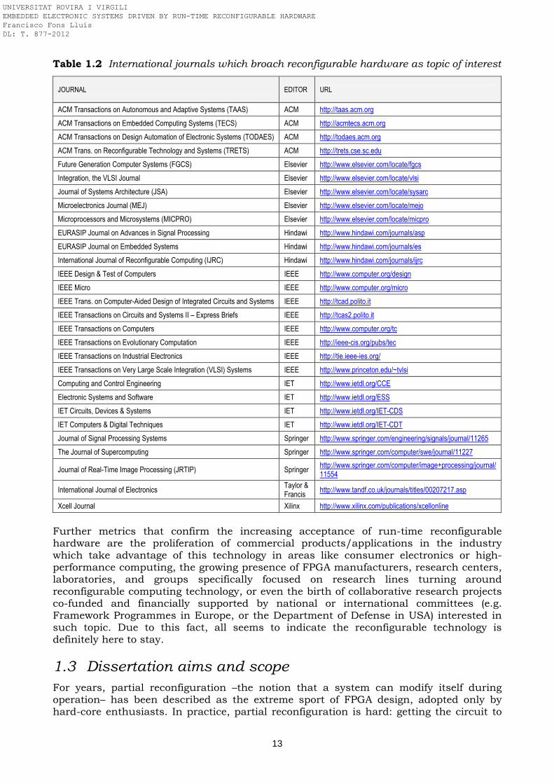
13
Table 1.2 International journals which broach reconfigurable hardware as topic of interest
JOURNAL
EDITOR URL
ACM Transactions on Autonomous and Adaptive Systems (TAAS) ACM http://taas.acm.org
ACM Transactions on Embedded Computing Systems (TECS) ACM http://acmtecs.acm.org
ACM Transactions on Design Automation of Electronic Systems (TODAES) ACM http://todaes.acm.org
ACM Trans. on Reconfigurable Technology and Systems (TRETS) ACM http://trets.cse.sc.edu
Future Generation Computer Systems (FGCS) Elsevier http://www.elsevier.com/locate/fgcs
Integration, the VLSI Journal Elsevier http://www.elsevier.com/locate/vlsi
Journal of Systems Architecture (JSA) Elsevier http://www.elsevier.com/locate/sysarc
Microelectronics Journal (MEJ) Elsevier http://www.elsevier.com/locate/mejo
Microprocessors and Microsystems (MICPRO) Elsevier http://www.elsevier.com/locate/micpro
EURASIP Journal on Advances in Signal Processing Hindawi http://www.hindawi.com/journals/asp
EURASIP Journal on Embedded Systems Hindawi http://www.hindawi.com/journals/es
International Journal of Reconfigurable Computing (IJRC) Hindawi http://www.hindawi.com/journals/ijrc
IEEE Design & Test of Computers IEEE http://www.computer.org/design
IEEE Micro IEEE http://www.computer.org/micro
IEEE Trans. on Computer-Aided Design of Integrated Circuits and Systems IEEE http://tcad.polito.it
IEEE Transactions on Circuits and Systems II – Express Briefs IEEE http://tcas2.polito.it
IEEE Transactions on Computers IEEE http://www.computer.org/tc
IEEE Transactions on Evolutionary Computation IEEE http://ieee-cis.org/pubs/tec
IEEE Transactions on Industrial Electronics IEEE http://tie.ieee-ies.org/
IEEE Transactions on Very Large Scale Integration (VLSI) Systems IEEE http://www.princeton.edu/~tvlsi
Computing and Control Engineering IET http://www.ietdl.org/CCE
Electronic Systems and Software IET http://www.ietdl.org/ESS
IET Circuits, Devices & Systems IET http://www.ietdl.org/IET-CDS
IET Computers & Digital Techniques IET http://www.ietdl.org/IET-CDT
Journal of Signal Processing Systems Springer http://www.springer.com/engineering/signals/journal/11265
The Journal of Supercomputing Springer http://www.springer.com/computer/swe/journal/11227
Journal of Real-Time Image Processing (JRTIP) Springer http://www.springer.com/computer/image+processing/journal/11554
International Journal of Electronics Taylor & Francis
http://www.tandf.co.uk/journals/titles/00207217.asp
Xcell Journal Xilinx http://www.xilinx.com/publications/xcellonline
Further metrics that confirm the increasing acceptance of run-time reconfigurable hardware are the proliferation of commercial products/applications in the industry which take advantage of this technology in areas like consumer electronics or high-performance computing, the growing presence of FPGA manufacturers, research centers, laboratories, and groups specifically focused on research lines turning around reconfigurable computing technology, or even the birth of collaborative research projects co-funded and financially supported by national or international committees (e.g. Framework Programmes in Europe, or the Department of Defense in USA) interested in such topic. Due to this fact, all seems to indicate the reconfigurable technology is definitely here to stay.
1.3 Dissertation aims and scope
For years, partial reconfiguration –the notion that a system can modify itself during operation– has been described as the extreme sport of FPGA design, adopted only by hard-core enthusiasts. In practice, partial reconfiguration is hard: getting the circuit to
UNIVERSITAT ROVIRA I VIRGILI EMBEDDED ELECTRONIC SYSTEMS DRIVEN BY RUN-TIME RECONFIGURABLE HARDWARE Francisco Fons Lluís DL: T. 877-2012
14
behave well while part of it is off reconfiguring, isolating the area that is being reconfigured from the part that is still operating, making the IOs behave properly during the transition, all of these issues can become complicated. However, the benefit to obtain from it is worth. The key advantage of reconfiguration technology falls on its silicon reusability. SRAM-based FPGAs offer today undeniable benefits in a world where products and its standards change day-by-day, going out of style in months as the technology progress advances. One might argue that usually there is a bigger FPGA where the application fits as a fixed hardware design, but the impact concerning cost or power consumption makes this other option, on most occasions, either inefficient or not competitive enough, or even simply unaffordable whether the final product is designed for mass production. Furthermore, the strongest obstacle for the massive introduction of FPGA devices in certain embedded applications –namely, the cost– is progressively ceasing to be a problem since the performance/cost trade-off delivered by state-of-the-art FPGAs makes them more and more affordable. That said, the introduction of partial reconfiguration technology in FPGA devices clearly contributes to reach this low cost target in many embedded application fields. The aim of this PhD dissertation is to investigate how dynamic partial reconfiguration technology can be used to gain competitive advantages in the implementation of embedded electronic systems typically synthesized by means of MCU-based platforms. For this, one of the entrusted missions comprises the evaluation of the state of this technology from an experimental viewpoint, especially concerning design flow, toolset and commercial devices available. The final goal is to do research on the feasibility of use of reconfigurable computing technology in the industry, on the one hand exploring the real possibilities of the current commercial programmable logic devices provided with dynamic partial reconfiguration capability and, on the other hand, evaluating the development flow and automatic tools linked to this technology – by following a rigorous methodology to solve specific real computing problems in embedded applications. Thus, this work focuses on the conception of a standard embedded system architecture to implement embedded applications driven by flexible hardware, noting that the design of an efficient reconfiguration engine –seamlessly coupled to the host CPU and the memory repository– is a key aspect to partition the application in functional tasks. Like this, it investigates the introduction of reconfigurable computing in specific applications fields whose functionality, apart from featuring parallel processing through the deployment of custom hardware accelerators, can be scheduled as a natural sequence of mutually exclusive tasks. The capability of run-time reconfigurable hardware technology to synthesize in programmable logic certain functionality partitioned in area and multiplexed in time by means of dynamic full/partial reconfiguration lets increase the functional density of these resources and fit the design into a smaller programmable logic device. The reuse of hardware resources to play a different role at each time results in cost and power consumption savings. As application scope, several end-user embedded applications highly demanded by the industry have been studied from a run-time reconfigurable hardware perspective. It is sometimes the case that a processing algorithm is designed and proven theoretically sound, presumably with a specific application in mind, but its practical application and detailed V&V are not fully explored and demonstrated, giving rise to critical and usually non-trivial issues when implementing it. Just to cover this aspect, these applications have been prototyped in real embedded FPGA/SoC platforms to take realistic conclusions about the proof of feasibility and benefits of this technology by evaluating the achieved results. In the end, this work seeks to serve the large community of researchers and professional engineers working on theoretical and practical aspects of reconfigurable computing. It is intended to bridge the gap between the theory and practice of embedded computing, contributing the greater community of researchers, practicing engineers, and industrial professionals who deal with designing, implementing or utilizing electronic systems which must satisfy real-time and low-cost processing constraints, to help to promote the use of reconfigurable computing for real-life products and applications in the industry.
UNIVERSITAT ROVIRA I VIRGILI EMBEDDED ELECTRONIC SYSTEMS DRIVEN BY RUN-TIME RECONFIGURABLE HARDWARE Francisco Fons Lluís DL: T. 877-2012
15
1.3.1 Contribution and thesis organization
In essence, this PhD dissertation pays attention to the introduction of reconfigurable computing in specific embedded applications where its use can lead to clear advantages in performance, cost and power metrics, demonstrating furthermore that such technology is mature enough to be exploited in the industry. With this goal in mind, this work is structured in fourteen chapters which are in turn organized in five sections: outline, state of the art, design and development, proofs of concept and use cases, and conclusions. The work is organized as a technical book split in chapters which are self-contained, each exploring a specific topic. Although one chapter can do some mention to other chapters, they try together to follow a consistent storyline. Besides, the bibliography is provided individually for each chapter. In this way, the reader should be able to plan the reading of this work chapter by chapter, allowing breaks or rest periods among chapters. Moreover, each chapter starts with a brief summary of its content, just to facilitate to the reader the distribution of matters along the book. The first section is composed of an introductory chapter which presents the reconfigurable computing concept and briefly reviews its history, from its birth until today. The second section encompasses the next two chapters and deals with the state of the art of reconfigurable hardware technology. Since the reconfigurable computing field is very dynamic, it covers relevant and varied matters in this arena, from technology aspects (reconfiguration design parameters, existing academic and commercial devices, technical open issues still pending to solve, etc) to other related measurables like research projects in progress today, derived patents under exploitation, etc. The third block comprises –in two more chapters– the design proposed by the author of a standard system architecture suitable for synthesizing embedded applications driven by run-time reconfigurable hardware. Special emphasis is put on the development of the reconfiguration engine since it becomes the most critical component of the flexible system and highly influences the efficiency of the whole target application. Both the system architecture and the reconfiguration engine design methodologies are compared with other approaches found in the literature. The fourth section focuses on the scope of application of this technology and is organized in seven chapters. The first of them is a survey of the application areas of reconfigurable computing; potential applications but also real applications and products which exploit PR like cryptography or software defined radio are reviewed. After this survey, up to six different use cases are studied by the author and prototyped in commercial FPGA or SoC devices. These use cases are distributed basically in three different application areas: control systems, arithmetic coprocessing, and high-performance computing. Regarding control, the proofs-of-concept of a PID controller and a fuzzy logic controller have been developed in an FPGA; concerning arithmetic coprocessing, two flexible computing systems like a 2D convolver and a CORDIC processor have been deployed in commercial FPGAs; and with regard to compute-intensive applications, two embedded systems have been designed. On the one hand, a biometric personal recognition system –to be exact, an automatic fingerprint authentication system or AFAS– has been completely mapped in different run-time reconfigurable platforms. On the other hand, another complex embedded system such as an automotive electronic control unit (ECU) –specifically, a body control module or body domain controller– has been designed to be deployed in a run-time reconfigurable SoC device. These six different scenarios are sufficiently significant and representative from an embedded computing viewpoint, with a wide enough diversity of features to analyse the implementation pros and cons of flexible hardware in contrast to other design technologies in use today. These case studies encompass the use of PR by covering from the fine reconfiguration of an element inside a coprocessor to the complete reconfiguration of a complex coprocessor in an application. Finally, the fifth section, composed of the last two chapters, concludes this dissertation by thinking over the current status of this technology, the goals reached up to now and the new milestones. It also points out the direction of the future author’s work.
UNIVERSITAT ROVIRA I VIRGILI EMBEDDED ELECTRONIC SYSTEMS DRIVEN BY RUN-TIME RECONFIGURABLE HARDWARE Francisco Fons Lluís DL: T. 877-2012
16
After this brief overview of the sections, a description of each chapter is stated next, highlighting the more relevant contributions of this dissertation. In chapter 1, the author outlines the scope of this work. It introduces first the concepts of reconfigurable computing and run-time reconfigurable hardware, and highlights then the more relevant milestones reached up to date in this field by putting them in perspective, just to realize both the difficulties that historically turned around this technology and its high computational potential achievable in return for this research effort. The momentum this technology is experiencing is evidenced through the large collection of dissemination means (especially conferences and journals) in place today. Chapter 2 gives a concise introduction to the implementation alternatives of electronic embedded systems. It is provided a detailed overview of the technical characteristics related to FPGA technology. It also does a revision to the challenges and open issues that the scientific community is facing today in this area. Chapter 3 describes the more notorious advances of this technology on the subject of relevant research projects conducted by the research community, publicated patents under exploitation, or PhD dissertations which turn about this computing paradigm, increasing thus the human resources and research groups that are getting involved in this matter. This chapter lists also a wide spectrum of devices and platforms coming from both academia and industry which support this technology. Chapter 4 introduces the standard embedded system architecture proposed by the author to deploy run-time reconfigurable computing. It presents the system breakdown in functional blocks, with special focus on practical issues concerning system performance. The system architecture proposed is compared then with some state-of-the-art system architectures found in the literature. As an extension of the previous chapter, the chapter 5 focuses exclusively on the design and development of the reconfiguration engine. This component takes charge of performing the online/offline full/partial reconfiguration of the programmable logic. It undoubtedly becomes the cornerstone of any run-time reconfigurable computing system. The efforts conducted in this area aimed at achieving a high reconfiguration bandwidth to minimize thus the reconfiguration latency in partially reconfigurable devices are presented here. The proposed reconfiguration controller is compared with state-of-the-art reconfiguration controllers. In chapter 6, apart from identifying many potential application areas of PR technology, some successful use cases, such as real applications in the industry or even commercial products already launched to the market, are overviewed. Chapter 7 concerns the implementation of a Proportional-Integral-Derivative or PID controller implemented in a small SoC –the Atmel AT94K FPSLIC device– composed of an MCU and an FPGA driven by run-time partial reconfiguration. The PID computing system is partitioned in three functional contexts (P, I and D computations, respectively) synthesized on hardware and time-multiplexed by the MCU at run-time, without interrupting the system execution. Similarly, chapter 8 encompasses the design of a general-purpose two-input one-output fuzzy logic controller driven by run-time reconfigurable hardware. A novel architecture is proposed to cope with the cost-effective implementation of digital controllers based on fuzzy logic. The controller, fueled by reconfigurability concepts, is architected to become general-purpose, able to be used in whatever two-input one-ouptut control application. Most of the flexibility reached in this concept is thanks to the flexible hardware. In chapter 9, the author proposes the design of a flexible 2D convolution computer based on run-time reconfigurable hardware. Two-dimensional convolution is a basic operation in digital signal processing that, although its computation is conceptually simple –a sum of products of constants by variables– its implementation is highly demanding in terms of computational power, especially when addressed to real-time embedded systems. This work brings an innovative approach oriented to dynamically reconfigurable hardware on a Xilinx Virtex-4 FPGA. All the configurable aspects of the convolver (kernel dimensions, operands resolution, constant coefficients, pipeline stages, etc) are handled in a partially
UNIVERSITAT ROVIRA I VIRGILI EMBEDDED ELECTRONIC SYSTEMS DRIVEN BY RUN-TIME RECONFIGURABLE HARDWARE Francisco Fons Lluís DL: T. 877-2012
17
reconfigurable region (PRR) of the device so they can be reconfigured on the fly in order to self-adapt the hardware structure of the 2D convolver to meet the optimum processing architecture required by the particular convolution to perform at each time, aimed at providing thus a universal solution. In chapter 10, it is presented the implementation of a trigonometric CORDIC computer based on a run-time reconfigurable architecture. Synthesized in the Atmel AT94K FPSLIC, the computer processes functions like sin(alpha), cos(alpha), atan2(b/a) and sqrt(a 2+b2)in hardware. The architecture lets switch from a trigonometric function to another by reconfiguring part of the coprocessor in only some few operation clocks. Chapter 11 pioneers the development of an automatic fingerprint authentication system on a run-time reconfigurable system-on-chip platform. The biometric recognition algorithm is partitioned in a sequence of image processing steps which are performed through custom hardware coprocessors following a batch process. Each of these computers is specifically designed to impressively enhance the performance of the algorithm in comparison to a software-based solution. In its turn, special care is taken to not to impact the system cost; for this, dynamic partial reconfiguration makes possible the reuse of the hardware resources along the execution of the different processing phases. This embedded application is prototyped in two different platforms: the Altera Excalibur SoC and the Xilinx Virtex-4 FPGA. In both cases, the system architecture is composed of an MCU (a hard-core ARM9 in Excalibur and a soft-core MicroBlaze in Virtex-4) and programmable logic. The author’s work has consisted in studying the entire biometric algorithm to identify the best partitioning of tasks and optimize then the synthesis of such processing in reconfigurable hardware. The study has covered the floorplaning and resizing of both PR and static regions in programmable logic in order to fit the application in the smallest FPGA platform possible while guaranteeing real-time performance. Regarding the partitioning of tasks, each image processing stage –determined by the reading of one image stored in the repository to be processed by the PR processor and sent back to the repository– delimits the proper way to do the spatial and temporal partitioning of the application. A key design aspect of this system consists in improving the bandwidth between the data repository and the reconfigurable computer. The system architecture and reconfiguration engine proposed in chapter 4 and 5, deployed now in this application example, proves to reduce hardware utilization significantly compared with static FPGA design solutions. Furthermore, the acceleration reached by means of hardware parallelism makes feasible to ensure real-time performance in the implementation of this biometric recognition system, fact that is not achievable when porting this same algorithm to only software in a PC platform based on a processor running at GHz. In chapter 12, the author details the design of an automotive electronic control unit (ECU) based on run-time programmable logic. This approach explores key features such as parallelism, customization, flexibility, redundancy and versatility of the reconfigurable hardware. Although it is only an early concept, is a pioneer in terms of merging both AUTOSAR and ISO 26262 with run-time reconfigurable hardware to perform hardware/software co-design for a full automotive embedded ECU system. This design is oriented to be prototyped in the Xilinx Zynq-7000 extensible processing platform, which combines a hard-wired ARM dual-core processor and 28-nanometer programmable logic equipped with dynamic partial reconfiguration capability. After overviewing the design and development of different embedded applications of interest and use in the industry based on run-time reconfigurable hardware, in chapter 13 the author reflects on the strengths and weaknesses of this technology today, highlighting all those aspects that make this computing paradigm attractive for the community but also all those issues or stoppers that need to be solved in the not-too-distant future in order to convert run-time reconfigurable hardware into a disruptive technology able to provide a clear competitive advantage to embedded electronic systems.
UNIVERSITAT ROVIRA I VIRGILI EMBEDDED ELECTRONIC SYSTEMS DRIVEN BY RUN-TIME RECONFIGURABLE HARDWARE Francisco Fons Lluís DL: T. 877-2012
18
Finally, chapter 14 reviews the deliverables generated by the author along all these years of research –through his participation in research projects, a part from publications in conferences, book chapters and journals– and concludes this work. The organization of this PhD dissertation composed of five sections and distributed in fourteen chapters aims to offer the reader a pleasant and friendly way to be introduced to the author’s work, combining theoretical and experimental aspects of run-time reconfigurable hardware, thinking about its pros and cons in contrast to other implementation alternatives, presenting innovative use cases, and evaluating, with real experiments, the state-of-the-art of this technology regarding commercial FPGA/SoC devices and EDA/CAD tools to be definitively exploited in the embedded computing world.
References
[Bobda, Springer 2007] C. Bobda, Introduction to reconfigurable computing – Architectures, algorithms and applications, Springer, ISBN 978-1-4020-6088-5, 2007.
[DeHon and Wawrzynek, DAC 1999] A. DeHon, J. Wawrzynek, Reconfigurable computing: what, why, and implications for design automation, Proceedings of the Design Automation Conference, pp. 610-615, 1999.
[Diessel et al., CDT 2000] O. Diessel, H. ElGindy, M. Middendorf, H. Schmeck, B. Schmidt, Dynamic scheduling of tasks on partially reconfigurable FPGAs, IEE Proc. of Computers and Digital Techniques, vol. 147, no. 3, pp. 181-188, 2000.
[Estrin, AHC 2002] G. Estrin, Reconfigurable computer origins: The UCLA fixed-plus-variable (F+V) structure computer, IEEE Annals of the History of Computing, vol. 24, no. 4, pp. 3-9, 2002.
[Estrin, WJCC 1960] G. Estrin, Organization of computer systems—The fixed plus variable structure computer, Proceedings of the Western Joint Computer Conference, pp. 33-40, 1960.
[Estrin and Turn, TEC 1963] G. Estrin, R. Turn, Automatic assignment of computations in a variable structure computer system, IEEE Transactions on Electronic Computers, vol. 12, no. 5, pp. 755-773, 1963.
[Hartenstein et al., FPL 1998] R.W. Hartenstein, M. Herz, F. Gilbert, Designing for Xilinx XC6200 FPGAs, Proc. of the Int. Conference on Field-Programmable Logic and Applications, LNCS, vol. 1482, pp. 29-38, Springer-Verlag, 1998.
[Hauck and Borriello, CADICS 1997] S. Hauck, G. Borriello, An evaluation of bipartitioning techniques, IEEE Transactions on Computer-Aided Design of Integrated Circuits and Systems, vol. 16, no. 8, pp. 849-866, 1997.
[Ling and Amano, FCCM 1993] X.P. Ling, H. Amano, WASMII: a data driven computer on a virtual hardware, Proceedings of IEEE Workshop on FPGAs for Custom Computing Machines, pp. 33-42, 1993.
[Lysaght and Rosenstiel, Springer 2005] P. Lysaght, W. Rosenstiel (Eds.), New algorithms, architectures and applications for reconfigurable computing, pp. 117-129, Springer, ISBN 978-1-4020-3127-4, 2005.
[Rodriguez-Andina et al., TIE 2007] J.J. Rodriguez-Andina, M.J. Moure, M.D. Valdes, Features, design tools, and application domains of FPGAs, IEEE Transactions on Industrial Electronics, vol. 54, no. 4, pp. 1810-1823, 2007.
[Sklyarov et al., Euromicro 1998] V. Sklyarov, N. Lau, R. Sal Monteiro, A. Melo, A. Oliveira, K. Kondratjuk, Design of virtual digital controllers based on dynamically reconfigurable FPGAs, Proc. of the Euromicro Conference, vol. 1, pp.200-203, 1998.
[Trimberger, FPGA 1998] S. Trimberger, Scheduling designs into a time-multiplexed FPGA, Proceedings of the International Symposium on Field Programmable Gate Arrays, pp. 153-160, 1998.
[Xilinx Inc., WP375 2010] P. Sundararajan, High Performance Computing Using FPGAs, Xilinx Inc., White Paper WP375 (v1.0), 2010.
[Xilinx Inc., Xcell 2004] Xilinx Staff, Celebrating 20 Years of Innovation, Xcell Journal, issue 48, pp.14-16, Xilinx Inc., Spring 2004.
[Zomaya, Springer 2006] A.Y. Zomaya, Handbook of nature-inspired and innovative computing, Springer, ISBN 978-0-387-40532-2, 2006.
UNIVERSITAT ROVIRA I VIRGILI EMBEDDED ELECTRONIC SYSTEMS DRIVEN BY RUN-TIME RECONFIGURABLE HARDWARE Francisco Fons Lluís DL: T. 877-2012

Part II
State of the Art
UNIVERSITAT ROVIRA I VIRGILI EMBEDDED ELECTRONIC SYSTEMS DRIVEN BY RUN-TIME RECONFIGURABLE HARDWARE Francisco Fons Lluís DL: T. 877-2012

UNIVERSITAT ROVIRA I VIRGILI EMBEDDED ELECTRONIC SYSTEMS DRIVEN BY RUN-TIME RECONFIGURABLE HARDWARE Francisco Fons Lluís DL: T. 877-2012
21
Chapter 2 Embedded systems and reconfigurable hardware Embedded electronic systems need to be synthesized as compact and efficient designs. In addition, due to the ever-increasing trend for adding new functionality into current applications and products, their architecture shall be flexible and scalable, able to let them absorb the continuous growth of computational power demanded to such embedded systems. Field programmable logic devices, mainly FPGAs, are nowadays a clear option to build versatile high-performance computing systems. To their original capability to synthesize a given functionality in programmable logic, the fact that the system can modify itself during operation, even on the fly, was soon understood as a strong added value which distinguishes FPGAs from other implementation alternatives, making thus the boundary between hardware and software more and more blurred. This chapter makes an introduction to the embedded computing world by overviewing the existing implementation options to build embedded systems. Regarding FPGA devices, they are clasified first from the programming technology point of view to, afterwards, give exclusive attention to SRAM-based dynamically reconfigurable FPGAs – the powerhorse of the reconfigurable computing paradigm today. The chapter tackles key FPGA design features like reconfiguration granularity, bitstream format or reconfiguration latency, and highlights the more relevant open issues to be addressed in the near future –related basically to bitstream manipulation matters– to propel forward the run-time reconfigurable hardware technology. It is considered today a promising design alternative in the embedded space, able to lead the next computing wave in the industry.
2.1 Embedded electronic systems
Embedded systems gain competitive advantages and add value to applications by embodying end-user functionality endowed with exclusive performance. In the last years, in the progress towards a more nomadic lifestyle, this trend has been accentuated by the emergence of many new mobile embedded devices in use in the daily routine. Examples of embedded systems span from control or security (e.g. smart cards) to mainstream consumer products in areas such as personal communication (e.g. cell phones), global positioning (e.g. navigation systems), personal computing (e.g. PDA), entertainment and many more. Although the implementation characteristics of an embedded system thoroughly depend on the specific application domain to which it is addressed, in general, the embedded design space shares a set of common, highly demanded technical constraints applicable to any embedded electronic system: limited size, weight and power consumption (i.e., SWaP), computation efficiency, security against attacks/reverse engineering, remote (in-field) system upgrade capability, functional flexibility and low cost are some of the unavoidable qualities that any embedded design shall be provided with. Hence, a successful product/application is one that, apart from performing the assigned functionality, is able to balance all these stringent technical features at the conception and development stages, being the cost the industry’s primary challenge today. Many implementation alternatives exist today to synthesize embedded electronic systems and each one meets specific demands, fitting well in a specific market niche; this is the main reason why each of these alternatives survives in the market.
2.1.1 Implementation alternatives
General-purpose processors (GPPs) are designed with the primary goal of providing acceptable performance on a wide variety of tasks rather than providing high performance on specific tasks. Driven by a software-oriented implementation perspective,
UNIVERSITAT ROVIRA I VIRGILI EMBEDDED ELECTRONIC SYSTEMS DRIVEN BY RUN-TIME RECONFIGURABLE HARDWARE Francisco Fons Lluís DL: T. 877-2012
22
Von Neumann or Harvard architectures found in CPUs of single-core or multicore microcontrollers (MCUs) provide a versatile platform able to perform a broad range of applications. As result, many applications can be deployed in such static hardware architecture via structured and flexible software programs described in simple lines of code. Nevertheless, their inherent constraints –e.g. the limited processing word size (typically 8-, 16- or 32-bit) leading to a performance degradation specially when the operations to be performed poorly match to the computational engine characteristics, or the sequential execution which causes a significant memory access bottleneck, or more recently, in multicore processors, the difficulty at the software end to program applications that can execute different parts in parallel on multiple cores, known as multicore programming crisis– give rise to a set of weaknesses which can make the software implementation alternative inadvisable for certain types of high-demanding applications, especially in time-critical scenarios. Other feasible general-purpose computing solutions are the digital signal processors (DSPs). Although they were originally conceived to applications of signal processing which make a great use of products and additions, at present the DSP is often joined to a CPU processor to make this platform more oriented to general-purpose computation. In addition, driven by the insatiable market demand for real-time high-definition 3D graphics, the graphics processor unit (GPU) has evolved into a highly parallel, multithreaded, many-core processor with high computational power and memory bandwidth, specifically well-suited to address problems that can be expressed as data-parallel computations –the same program is executed on many data elements in parallel– with high arithmetic intensity, e.g. 3D rendering. Moreover, with the concept of general-purpose computing on graphics processing units (GPGPU), NVIDIA introduced a general-purpose parallel computing architecture called compute unified device architecture (CUDA) to extend thus the GPU application field to applications requiring massive vector operations, not only graphical operations. The model for GPGPU is to use a CPU and GPU together in a heterogeneous co-processing computing model. The sequential part of the application runs on the CPU and the computationally intensive part is accelerated by the GPU, composed of hundreds of processor cores. However, this architecture is not suited for applications that merge at the same time parallel processing and other types of specific processing that do not match the GPU or CPU architecture. Going from one extreme to another, application-specific integrated circuits (ASICs) or application-specific standard products (ASSPs) are designed for a specific application domain and, hence, each ASIC or ASSP deploys fixed functionality with superior performance since it is tailored to a specific algorithm or problem and no extra overhead for instruction interpretation is needed and no extra circuitry is deployed to cover a more general problem. However, the ASICs restrict the flexibility of the circuits by excluding any posterior design optimization, upgrade or bug fixing capability after fabrication. Besides, their non-recurring engineering (NRE) costs make this technology prohibitive or inaccessible to small and medium enterprises (SMEs) and they typically need high production volumes to make this option affordable. At midway between the high performance of ASICs and the flexibility of purely-software approaches synthesized on GPPs, FPGA devices are used in the market for more than glue logic, MCU hardware emulation and ASIC prototyping. Its exploitation is more and more usual in embedded computing design since, as the electronics density of these systems increases to satisfy the growing functional demands of new end-user applications, FPGA vendors are delivering bigger devices that boast lower power consumption rates at more competitive prices. Only very high-volume and highly power-sensitive products remain today out-of-reach for FPGAs, and the border of having cost advantage from custom circuits is raising to higher production volumes continually. Thus, FPGA devices, either stand-alone or used in conjunction with a general-purpose processor, are being used in a variety of applications since the developer can tailor the computer architecture to the particular application needs to accomplish an efficient solution, by mapping particular algorithms in hardware and matching the processor
UNIVERSITAT ROVIRA I VIRGILI EMBEDDED ELECTRONIC SYSTEMS DRIVEN BY RUN-TIME RECONFIGURABLE HARDWARE Francisco Fons Lluís DL: T. 877-2012
23
structure to the needs of the demanded computation. Moreover, due to the rapid technology advancement, the design and development of embedded systems has been relentlessly merged with integrated circuit design. This continuous growth has brought the technology over the border where it can now accommodate complete embedded systems on a single chip. Today’s silicon technology allows building embedded processors as part of SoC devices comprising up to a billion transistors usable as programmable logic on a single die [Nurmi, Springer 2007]. FPGAs have become now complete SoC platforms that combine a whole MCU (processor, memory and peripherals) with user programmable fabric into a single device to implement there custom coprocessors or accelerators required by the end-user application. This results a leading option to balance parallelism and flexibility in an efficient way to deploy embedded applications. Moreover, one definitive advantage of FPGAs against the rest of alternatives is their inherent reconfigurability. Reconfigurable computing, reinforced with the widespread availability of commercial SRAM-based FPGAs, is intended to fill in the gap between both static hardware-oriented and software-oriented implementation strategies by customizing the hardware architecture at the instruction level for every application, where the optimal grain needed for the application matches the instruction granularity of the hardware computer deployed in each case. It offers the advantages of custom and scalable, parallel hardware processing for each of the processing tasks the embedded application demands. As summary, GPPs, MCUs, DSPs, ASICs, FPGAs, GPUs and SoCs are nowadays the major options to develop embedded electronic systems. Independently of the chosen alternative, the demand for low cost and low power consumption and computation performance is an unavoidable feature. This dissertation focuses exclusively on SRAM-based FPGA devices to deploy embedded electronic systems driven by run-time reconfigurable hardware technology.
2.2 Field programmable gate arrays
FPGA devices emerged as an implementation alternative oriented to the acceleration of computationally intensive tasks by exploiting hardware parallelism. Many applications characterized by the processing of large amounts of data are well suited for exploiting parallelism, e.g. image processing, therefore the use of an FPGA device can bring an increase in performance compared to a sequential implementation on GPPs. Moreover, along the time, FPGA devices have experienced an outstanding growth in resources, ranging up to some billions of transistors today –allowing already the implementation of a full application in a single chip– and gaining acceptance the trend of converting the FPGA into a SoC device which merges programmable logic and a MCU in the same chip. Hence, by means of hardware/software partitioning it is possible to meet a solution of two computing worlds – digital hardware design to fit in logic the computationally intensive tasks of any target application and embedded software handled by the CPU for the remaining processing tasks that exhibit little parallelism. To this original view, it was realized that the benefits of logic cell level specialization could be extended by reconfiguring circuit resources at run-time. Reconfiguration accentuated the interest in FPGA devices by providing a clear competitive advantage over other traditional alternatives based on static hardware implementations. The field of programmable logic evidenced a significant interest in the addition of dynamic reconfiguration capabilities to conventional FPGAs. The fact that the configuration data of certain FPGAs can be reprogrammed –either offline or on-the-fly– an unlimited number of times incited the research on partial reconfiguration, becoming a potential implementation alternative to achieve unmatched performance and flexibility over conventional systems, especially for compute-intensive and cost-sensitive applications. It represents a step forward in the design and development of digital systems through flexible programmable logic since it allows to reduce the hardware resources required for performing the specific computation by reusing them along the execution time if every
UNIVERSITAT ROVIRA I VIRGILI EMBEDDED ELECTRONIC SYSTEMS DRIVEN BY RUN-TIME RECONFIGURABLE HARDWARE Francisco Fons Lluís DL: T. 877-2012
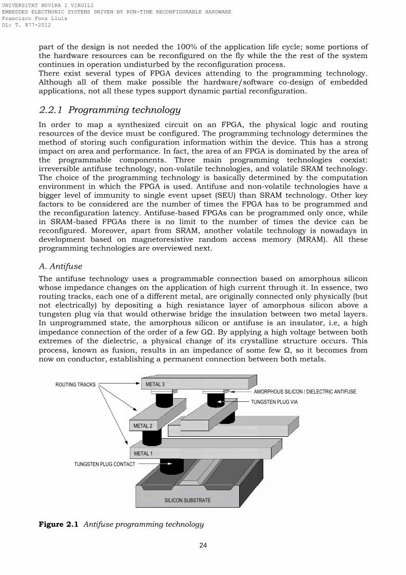
24
part of the design is not needed the 100% of the application life cycle; some portions of the hardware resources can be reconfigured on the fly while the the rest of the system continues in operation undisturbed by the reconfiguration process. There exist several types of FPGA devices attending to the programming technology. Although all of them make possible the hardware/software co-design of embedded applications, not all these types support dynamic partial reconfiguration.
2.2.1 Programming technology
In order to map a synthesized circuit on an FPGA, the physical logic and routing resources of the device must be configured. The programming technology determines the method of storing such configuration information within the device. This has a strong impact on area and performance. In fact, the area of an FPGA is dominated by the area of the programmable components. Three main programming technologies coexist: irreversible antifuse technology, non-volatile technologies, and volatile SRAM technology. The choice of the programming technology is basically determined by the computation environment in which the FPGA is used. Antifuse and non-volatile technologies have a bigger level of immunity to single event upset (SEU) than SRAM technology. Other key factors to be considered are the number of times the FPGA has to be programmed and the reconfiguration latency. Antifuse-based FPGAs can be programmed only once, while in SRAM-based FPGAs there is no limit to the number of times the device can be reconfigured. Moreover, apart from SRAM, another volatile technology is nowadays in development based on magnetoresistive random access memory (MRAM). All these programming technologies are overviewed next. A. Antifuse
The antifuse technology uses a programmable connection based on amorphous silicon whose impedance changes on the application of high current through it. In essence, two routing tracks, each one of a different metal, are originally connected only physically (but not electrically) by depositing a high resistance layer of amorphous silicon above a tungsten plug via that would otherwise bridge the insulation between two metal layers. In unprogrammed state, the amorphous silicon or antifuse is an insulator, i.e, a high impedance connection of the order of a few GΩ. By applying a high voltage between both extremes of the dielectric, a physical change of its crystalline structure occurs. This process, known as fusion, results in an impedance of some few Ω, so it becomes from now on conductor, establishing a permanent connection between both metals.
Figure 2.1 Antifuse programming technology
SILICON SUBSTRATE
TUNGSTEN PLUG CONTACT
METAL 1
METAL 2
METAL 3 AMORPHOUS SILICON / DIELECTRIC ANTIFUSE
TUNGSTEN PLUG VIA
ROUTING TRACKS
UNIVERSITAT ROVIRA I VIRGILI EMBEDDED ELECTRONIC SYSTEMS DRIVEN BY RUN-TIME RECONFIGURABLE HARDWARE Francisco Fons Lluís DL: T. 877-2012
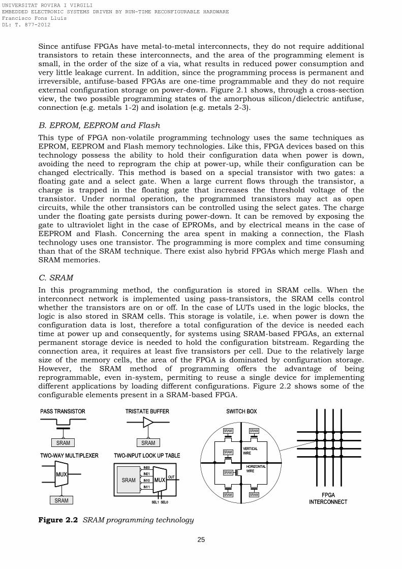
25
Since antifuse FPGAs have metal-to-metal interconnects, they do not require additional transistors to retain these interconnects, and the area of the programming element is small, in the order of the size of a via, what results in reduced power consumption and very little leakage current. In addition, since the programming process is permanent and irreversible, antifuse-based FPGAs are one-time programmable and they do not require external configuration storage on power-down. Figure 2.1 shows, through a cross-section view, the two possible programming states of the amorphous silicon/dielectric antifuse, connection (e.g. metals 1-2) and isolation (e.g. metals 2-3). B. EPROM, EEPROM and Flash
This type of FPGA non-volatile programming technology uses the same techniques as EPROM, EEPROM and Flash memory technologies. Like this, FPGA devices based on this technology possess the ability to hold their configuration data when power is down, avoiding the need to reprogram the chip at power-up, while their configuration can be changed electrically. This method is based on a special transistor with two gates: a floating gate and a select gate. When a large current flows through the transistor, a charge is trapped in the floating gate that increases the threshold voltage of the transistor. Under normal operation, the programmed transistors may act as open circuits, while the other transistors can be controlled using the select gates. The charge under the floating gate persists during power-down. It can be removed by exposing the gate to ultraviolet light in the case of EPROMs, and by electrical means in the case of EEPROM and Flash. Concerning the area spent in making a connection, the Flash technology uses one transistor. The programming is more complex and time consuming than that of the SRAM technique. There exist also hybrid FPGAs which merge Flash and SRAM memories. C. SRAM
In this programming method, the configuration is stored in SRAM cells. When the interconnect network is implemented using pass-transistors, the SRAM cells control whether the transistors are on or off. In the case of LUTs used in the logic blocks, the logic is also stored in SRAM cells. This storage is volatile, i.e. when power is down the configuration data is lost, therefore a total configuration of the device is needed each time at power up and consequently, for systems using SRAM-based FPGAs, an external permanent storage device is needed to hold the configuration bitstream. Regarding the connection area, it requires at least five transistors per cell. Due to the relatively large size of the memory cells, the area of the FPGA is dominated by configuration storage. However, the SRAM method of programming offers the advantage of being reprogrammable, even in-system, permiting to reuse a single device for implementing different applications by loading different configurations. Figure 2.2 shows some of the configurable elements present in a SRAM-based FPGA.
Figure 2.2 SRAM programming technology
SRAM SRAM
MUX
SRAM
SRAMSRAM
SRAM
SRAM
SRAM
SRAM
FPGAINTERCONNECT
VERTICALWIRE
HORIZONTALWIRE
MUXSRAM
PASS TRANSISTOR TRISTATE BUFFER
TWO-WAY MULTIPLEXER TWO-INPUT LOOK UP TABLE
SWITCH BOX
IN00
IN01
IN10
IN11
OUT
SEL1 SEL0
SRAM SRAM
MUX
SRAM
SRAMSRAM
SRAM
SRAM
SRAM
SRAM
FPGAINTERCONNECT
VERTICALWIRE
HORIZONTALWIRE
MUXSRAM
PASS TRANSISTOR TRISTATE BUFFER
TWO-WAY MULTIPLEXER TWO-INPUT LOOK UP TABLE
SWITCH BOX
IN00
IN01
IN10
IN11
OUT
SEL1 SEL0
UNIVERSITAT ROVIRA I VIRGILI EMBEDDED ELECTRONIC SYSTEMS DRIVEN BY RUN-TIME RECONFIGURABLE HARDWARE Francisco Fons Lluís DL: T. 877-2012
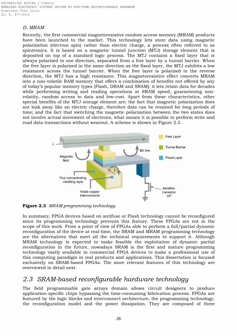
26
D. MRAM
Recently, the first commercial magnetoresistive random access memory (MRAM) products have been launched to the market. This technology lets store data using magnetic polarization (electron spin) rather than electric charge, a process often referred to as spintronics. It is based on a magnetic tunnel junction (MTJ) storage element that is deposited on top of a standard logic process. The MTJ contains a fixed layer that is always polarized in one direction, separated from a free layer by a tunnel barrier. When the free layer is polarized in the same direction as the fixed layer, the MTJ exhibits a low resistance across the tunnel barrier. When the free layer is polarized in the reverse direction, the MTJ has a high resistance. This magnetoresistive effect converts MRAM into a non-volatile RAM memory that offers a combination of benefits not offered by any of today’s popular memory types (Flash, DRAM and SRAM): it lets retain data for decades while performing writing and reading operations at SRAM speed, guaranteeing non-volatity, random access to data and low-cost. Apart from these characteristics, other special benefits of the MTJ storage element are: the fact that magnetic polarization does not leak away like an electric charge, therefore data can be retained for long periods of time; and the fact that switching the magnetic polarization between the two states does not involve actual movement of electrons, what means it is possible to perform write and read data transactions without wearout. A scheme is shown in Figure 2.3.
Figure 2.3 MRAM programming technology In summary, FPGA devices based on antifuse or Flash technology cannot be reconfigured since its programming technology prevents this feature. These FPGAs are not in the scope of this work. From a point of view of FPGAs able to perform a full/partial dynamic reconfiguration of the device at real-time, the SRAM and MRAM programming technology are the alternatives that meet all the technical requirements to support it. Although MRAM technology is expected to make feasible the exploitation of dynamic partial reconfiguration in the future, nowadays SRAM is the first and mature programming technology vastly available in commercial FPGA devices to make a professional use of this computing paradigm in real products and applications. This dissertation is focused exclusively on SRAM-based FPGAs. The more relevant features of this technology are overviewed in detail next.
2.3 SRAM-based reconfigurable hardware technology
The field programmable gate arrays domain allows circuit designers to produce application-specific chips bypassing the time-consuming fabrication process. FPGAs are featured by the logic blocks and interconnect architecture, the programming technology, the reconfiguration model and the power dissipation. They are composed of three
UNIVERSITAT ROVIRA I VIRGILI EMBEDDED ELECTRONIC SYSTEMS DRIVEN BY RUN-TIME RECONFIGURABLE HARDWARE Francisco Fons Lluís DL: T. 877-2012
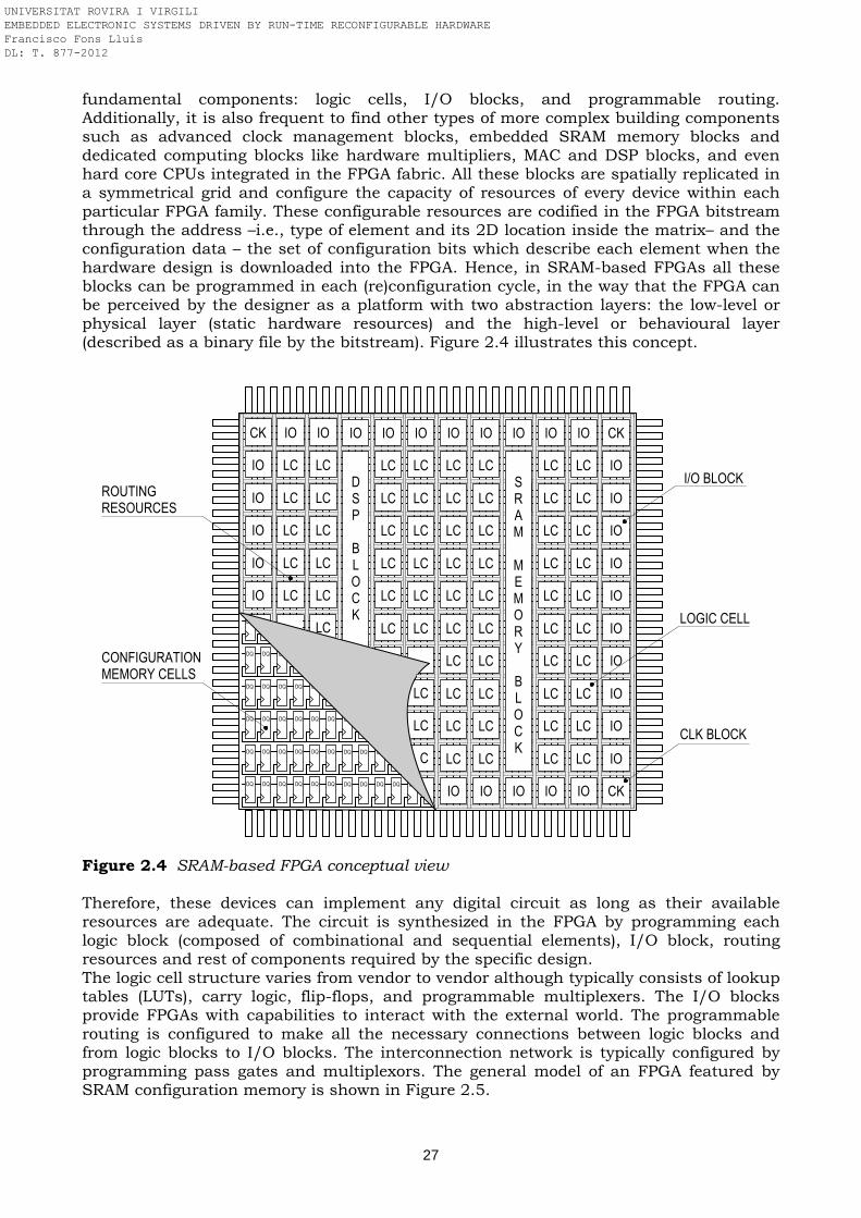
27
fundamental components: logic cells, I/O blocks, and programmable routing. Additionally, it is also frequent to find other types of more complex building components such as advanced clock management blocks, embedded SRAM memory blocks and dedicated computing blocks like hardware multipliers, MAC and DSP blocks, and even hard core CPUs integrated in the FPGA fabric. All these blocks are spatially replicated in a symmetrical grid and configure the capacity of resources of every device within each particular FPGA family. These configurable resources are codified in the FPGA bitstream through the address –i.e., type of element and its 2D location inside the matrix– and the configuration data – the set of configuration bits which describe each element when the hardware design is downloaded into the FPGA. Hence, in SRAM-based FPGAs all these blocks can be programmed in each (re)configuration cycle, in the way that the FPGA can be perceived by the designer as a platform with two abstraction layers: the low-level or physical layer (static hardware resources) and the high-level or behavioural layer (described as a binary file by the bitstream). Figure 2.4 illustrates this concept. Figure 2.4 SRAM-based FPGA conceptual view Therefore, these devices can implement any digital circuit as long as their available resources are adequate. The circuit is synthesized in the FPGA by programming each logic block (composed of combinational and sequential elements), I/O block, routing resources and rest of components required by the specific design. The logic cell structure varies from vendor to vendor although typically consists of lookup tables (LUTs), carry logic, flip-flops, and programmable multiplexers. The I/O blocks provide FPGAs with capabilities to interact with the external world. The programmable routing is configured to make all the necessary connections between logic blocks and from logic blocks to I/O blocks. The interconnection network is typically configured by programming pass gates and multiplexors. The general model of an FPGA featured by SRAM configuration memory is shown in Figure 2.5.
DQ
DQ
DQ
DQ
DQ
DQ
DQ
DQ
DQ
DQ
DQ
C
IO
IO
IO
CK
IO
IO
IO
IO
IO
IO
CK
IO
LC
LC
IO
LC
LC
LC
LC
LC
IO
LC
LC
LC
IO
LC
LC
LC
LC
LC
LC
IO
LC
LC
LC
IO
LC
LC
LC
LC
LC
IO
LC
LC
LC
IO
LC
LC
LC
LC
LC
IO
LC
LC
LC
IO
LC
LC
LC
LC
LC
IO
LC
LC
LC
LC
LC
LC
LC
IO
LC
LC
LC
LC
LC
IO
LC
LC
LC
LC
LC
IO
LC
LC
LC
LC
LC
IO
LC
LC
LC
LC
IO
IO
IO
IO
IO
DQ
IO
CK
DQ
DQ
DQ
DQ
DQ
DQ
DQ
DQ
DQ
DQ
DQ
DQ
DQ
DQ
DQ
DQ
DQ
DQ
DQ
DQ
DQ
DQ
DQ
DQ
DQ
DQ
DQ
DQ
DQ
I/O BLOCK
LOGIC CELL
ROUTING RESOURCES
CONFIGURATION MEMORY CELLS
S R A M
M E M O R Y
B L O C K
D S P
B L O C K
CLK BLOCK
UNIVERSITAT ROVIRA I VIRGILI EMBEDDED ELECTRONIC SYSTEMS DRIVEN BY RUN-TIME RECONFIGURABLE HARDWARE Francisco Fons Lluís DL: T. 877-2012
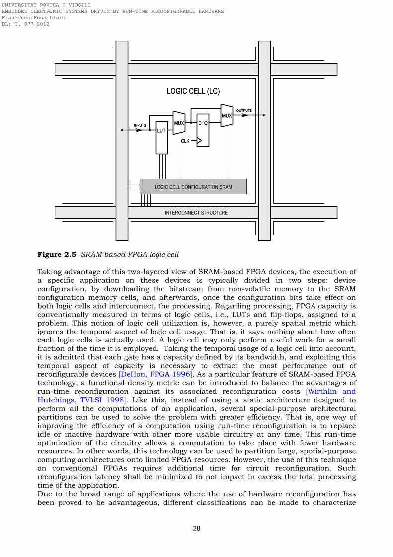
28
Figure 2.5 SRAM-based FPGA logic cell Taking advantage of this two-layered view of SRAM-based FPGA devices, the execution of a specific application on these devices is typically divided in two steps: device configuration, by downloading the bitstream from non-volatile memory to the SRAM configuration memory cells, and afterwards, once the configuration bits take effect on both logic cells and interconnect, the processing. Regarding processing, FPGA capacity is conventionally measured in terms of logic cells, i.e., LUTs and flip-flops, assigned to a problem. This notion of logic cell utilization is, however, a purely spatial metric which ignores the temporal aspect of logic cell usage. That is, it says nothing about how often each logic cells is actually used. A logic cell may only perform useful work for a small fraction of the time it is employed. Taking the temporal usage of a logic cell into account, it is admitted that each gate has a capacity defined by its bandwidth, and exploiting this temporal aspect of capacity is necessary to extract the most performance out of reconfigurable devices [DeHon, FPGA 1996]. As a particular feature of SRAM-based FPGA technology, a functional density metric can be introduced to balance the advantages of run-time reconfiguration against its associated reconfiguration costs [Wirthlin and Hutchings, TVLSI 1998]. Like this, instead of using a static architecture designed to perform all the computations of an application, several special-purpose architectural partitions can be used to solve the problem with greater efficiency. That is, one way of improving the efficiency of a computation using run-time reconfiguration is to replace idle or inactive hardware with other more usable circuitry at any time. This run-time optimization of the circuitry allows a computation to take place with fewer hardware resources. In other words, this technology can be used to partition large, special-purpose computing architectures onto limited FPGA resources. However, the use of this technique on conventional FPGAs requires additional time for circuit reconfiguration. Such reconfiguration latency shall be minimized to not impact in excess the total processing time of the application. Due to the broad range of applications where the use of hardware reconfiguration has been proved to be advantageous, different classifications can be made to characterize
LOGIC CELL (LC)
CLK
D Q
LUT
MUX
INTERCONNECT STRUCTURE
INPUTS
MUXOUTPUTS
LOGIC CELL CONFIGURATION SRAM
LOGIC CELL (LC)
CLK
D Q
LUT
MUX
INTERCONNECT STRUCTURE
INPUTS
MUXOUTPUTS
LOGIC CELL CONFIGURATION SRAM
UNIVERSITAT ROVIRA I VIRGILI EMBEDDED ELECTRONIC SYSTEMS DRIVEN BY RUN-TIME RECONFIGURABLE HARDWARE Francisco Fons Lluís DL: T. 877-2012
29
reconfigurable FPGA devices paying attention to specific properties. Following sections provide a review of the more relevant features which define a reconfigurable device. It can be stated that, according to all this set of characteristics, the choice for the best suited reconfigurable device is strongly related to the application itself where this device is intended for deploying certain functionality, with a defined level of performance and cost.
2.3.1 Reconfiguration model
Reconfigurable hardware devices can be classified in several categories in terms of the reconfiguration method used [Compton and Hauck, ACM 2002]: A. Single context
A single context FPGA is architected with an only plane of hardware resources distributed along the device. Such resources are configured by downloading the configuration bitstream. Since the access to the configuration memory is restricted by a sequential flow, the entire FPGA must be reconfigured even if only a portion of the chip needs to be changed. Therefore, in order to implement run-time reconfiguration using a single context FPGA, the configurations are grouped into contexts and each full context is transferred to the device when needed. Although from an architectural viewpoint this reconfiguration mechanism is simple, a good partitioning of the target application in configuration contexts is essential to minimize the total reconfiguration latency. Most commercial SRAM-based FPGAs are of this style, like Altera Cyclone and Stratix families. B. Partially reconfigurable
Often, only a part of the FPGA resources require modification. In these situations, a partial reconfiguration of the FPGA is needed rather than a full reconfiguration. In a partially reconfigurable (PR) FPGA, a portion of the FPGA can be reconfigured without interrupting the operation of the rest of the circuit, which may continue the execution while the reconfiguration is in progress. This type of FPGA architecture increases the efficiency of reconfiguration by reducing the reconfiguration overhead. Besides, as it is possible to overlap the computation of some parts of the device with the reconfiguration of the other parts, this has the benefit of potentially hiding partially or totally the reconfiguration latency. However, for this the bitstream format shall contain the specific position of the addressed resource: since address information must be supplied with configuration data, the total amount of information transferred to the reconfigurable hardware may be greater that what is required with a single context design where in this case the address can be implicitly specified through the sequence of the bitstream information. The reconfigurable partition of a partially reconfigurable FPGA is typically organized in a rectangular area. In function of the dimensional characteristics of such reconfigurable surface, partially reconfigurable FPGAs are classified in two groups:
One-dimensional (1D) reconfiguration In these FPGAs, the reconfiguration is performed in regions that are extended along the vertical dimension of the reconfigurable hardware device. While the designer can define the horizontal length of the reconfigurable region, the vertical length is fixed to the complete vertical dimension of the device. An example of partially reconfigurable FPGA with 1D reconfiguration models is the Xilinx Virtex-II FPGA.
Two-dimensional (2D) reconfiguration The 2D reconfigurable FPGAs treat PR regions or partitions as rectangles to be placed at an arbitrary position inside the larger 2D sea of resources distributed along the device. 2D models have been shown to lead to better device utilization. In this way, the designer can define both horizontal and vertical dimensions of the PR partition, although typically it is necessary to meet some minor restrictions concerning the total size of the PR partition selected. An example of commercial FPGA device which meets
UNIVERSITAT ROVIRA I VIRGILI EMBEDDED ELECTRONIC SYSTEMS DRIVEN BY RUN-TIME RECONFIGURABLE HARDWARE Francisco Fons Lluís DL: T. 877-2012
30
the 2D reconfiguration model is the Xilinx Virtex-4 device. Although the minimum number of vertical configurable logic blocks (CLBs) which must be reconfigured is still fixed to a specific grain (16 CLBs), the reconfiguration time and the partial bitstream size are decreased, providing a greater flexibility in choosing the best floorplanning and mapping of reconfigurable tasks inside the device.
Apart from this classification, there exist a technique that allows effective 2D partial reconfiguration in 1D partially reconfigurable FPGA devices so-called Read-Modify-Writeback [Paulsson et al., FPL 2007]. This method was developed for increasing the flexibility when performing dynamic partial reconfiguration on Xilinx Virtex-II FPGAs. In this way, the inherent 1D (column-based) reconfiguration of Virtex-II and Virtex-II Pro devices is somehow converted to a 2D reconfiguration. This approach exploits the possibility for reading back configuration data from the FPGA configuration memory, modifying it and writing it back to the configuration memory, although the write operation still affect all the column dimension. C. Multi-context
A multi-context FPGA can be seen as a set of planes of resources from single context FPGAs working in a multiplexed way, where only one of these configuration planes is active at any given time. Therefore, the multi-context FPGA includes multiple memory bits for each programming bit location, in the way that these memory bits can be thought of as multiple planes of configuration information. As result, this model allows for the background loading of one of the contexts while another is active and in execution. One plane of configuration information can be active at a given moment and the device can quickly switch among different planes or contexts of already programmed configurations. Switching between two different contexts can take place in one clock cycle (i.e., order of nanoseconds) since there is no need to load the configuration data just at that moment. Thus, although reconfiguring a context should take the same time as in a single context device, such reconfiguration can be hidden and performed in parallel while other context is operating. In return for it, the additional memory required to store the configuration data substantially increases the complexity and chip area of the FPGA, since the amount of virtual hardware emulated by a multi-context FPGA with n contexts is limited to n times the physical hardware in that FPGA. Regarding the amount of resources reconfigured, multi-context devices can support both full and partial reconfiguration. Full reconfiguration corresponds to devices architected with only one select control bus which is common to all the context multiplexors affecting all the FPGA resources. Partial reconfiguration is feasible by having individual select control lines distributed along the device resources and assigned each one to a different configuration bit of the device. An example of multi-context FPGA is FIPSOC from SIDSA which, although no longer in the market, admits partial reconfiguration of rectangular blocks and also full reconfiguration at run-time in only one clock cycle.
2.3.2 Granularity
The grain of reconfigurable logic devices refers to the physical size of the smallest element or block that can be reconfigured without interacting with the rest of resources in the device. It is a critical point for silicon efficiency in reconfigurable hardware technology and determines the minimum atomic change possible. There are several types of reconfigurable devices attending to configuration granularity of the logic elements that constitute the device; a distinction is made between fine- and coarse-grain architectures, as well as a fusion of both. Like this, configuration information or bitstream refers to the data bits sent to the device to set the state of all its resources, logic and interconnection. A fine-grained FPGA architecture lets change a minimum part of the device, up to a bit-level, between a configuration cycle and the following one, for instance to change a connection bit or a LUT-based truth table bit. On the contrary, a coarse-grained
UNIVERSITAT ROVIRA I VIRGILI EMBEDDED ELECTRONIC SYSTEMS DRIVEN BY RUN-TIME RECONFIGURABLE HARDWARE Francisco Fons Lluís DL: T. 877-2012
31
architecture applies the same procedure to a bigger element or group of elements, for instance a whole logic cell (composed of LUT, flip-flop and local interconnections) or a specific processing block. Both FPGA configuration time and configuration memory size directly depend on the FPGA grain. Lower granularity provides more flexibility in adapting the hardware to the computation structure; however, it has a major performance penalty due to larger delays when constructing computation modules of a larger size using smaller functional units. In addition, fine-grain and coarse-grain devices have differences in the configuration time because coarse-grain devices typically need less data bits for bitstream storage; therefore, their configuration time is shorter. A. Fine-grain achitecture
In fine-grained reconfigurable architectures, the functionality of the hardware is specified at the bit-level and the programmable interconnect is manipulated as individual wires. Fine-grained architectures are efficient for complex bit-oriented computations or bit-level masking and filtering. However, this fine-grained flexibility comes at the cost of additional silicon and configuration time overhead and an increment in the bitstream storage capacity. Typically, an FPGA architecture is considered fine-grained when its datapath width is four bits or less. The Atmel AT40K FPGA is an example of fine-grained reconfigurable architecture. B. Coarse-grain architecture
As reconfigurable fabrics grow in size and are migrated to more advanced technologies, the cost in terms of both speed and power of the interconnect part of a reconfigurable fabric rises. Designers are responding to this by increasing the granularity of their logic units, thereby reducing the amount of interconnect needed. As example, some FPGA have moved the structure of LUTs from 4-inputs to 6-inputs. Coarse-grained reconfigurable architectures contain word-level function units such as multipliers and the programmable interconnect is manipulated with n-bit buses. An example of coarse-grained architecture corresponds to the XPP processor from PACT, constituted by a set of processing array elements (PAEs). C. Hybrid architecture
A hybrid architecture comprising both fine- and coarse-grained elements is also possible. This hybrid archichecture, named also multi-grain or heterogeneous architecture, combines the best of both worlds: it can implement word-level algorithms much more efficiently than fine-grained architectures and can also implement bit-level algorithms much more efficiently than coarse-grained architectures. Such FPGA devices embed coarse-grained components into their fine-grained architecture.
2.3.3 Reconfigurability features
Since their introduction, SRAM-based FPGAs have received increasing attention due to their potential as reconfigurable logic devices, with the ability to implement arbitrary functionality and be reprogrammed an unlimited number of times during their lifetime, both off-line and on the fly [Hadley and Hutchings, FCCM 1995]. Reconfiguration features can be classified according to certain basic criteria such as device activity, amount of resources reconfigured, reconfiguration interface, and so on. All these characteristics are overviewed next. A. Device activity during reconfiguration
Paying attention to the number of reconfigurations performed during the application execution or to the device activity while the reconfiguration is in progress, reconfigurable FPGAs are classified in different categories [Shoa and Shirani, VLSI 2005]:
UNIVERSITAT ROVIRA I VIRGILI EMBEDDED ELECTRONIC SYSTEMS DRIVEN BY RUN-TIME RECONFIGURABLE HARDWARE Francisco Fons Lluís DL: T. 877-2012
32
Static (compile-time) reconfiguration Depending on the technological features of the FPGA device or on the application for which it is deployed, in certain applications the reconfiguration is not used. That situation occurs in the so-called static or compile-time reconfigurable systems. This name comes from the fact that the entire configuration is determined at compile-time and does not change throughout system operation; a single design is loaded into the full FPGA after a system power-on-reset and it remains unchanged for all the application lifetime, until the application finishes. In the past, most FPGA designs have been architected in this way, being static in nature.
Shutdown reconfiguration Certain FPGA devices allow reconfiguring the device multiple times during the application execution. However, this reconfiguration cannot be performed while the device is in operation. In such case, the functionality of the circuit does not change while the application is running and it must be halted during the reconfiguration period. Hence, to reconfigure this type of device it is required to stop it first (i.e., keep the device in reset) and reconfigure then its logic off-line. In other words, these devices have mutually exclusive operational and configuration modes since there is no mechanism to allow simultaneous operation and configuration.
Active (dynamic or run-time) reconfiguration Systems in which the configuration of the reconfigurable hardware can change during run-time are referred to as dynamic or run-time reconfigurable systems. Active reconfiguration allows that parts of the system may be reconfigured while other parts are running, without disruption. In this scenario, the application is partitioned into time-multiplexed tasks. Each task is implemented as a distinct configuration which can be downloaded into the FPGA at run-time during application operation.
B. Amount of device resources reconfigured
FPGA reconfiguration consists in reprogramming the configuration memory by downloading a sequence of bits known as bitstream onto it. These data define the operation (i.e. functionality) to be processed by the combinational and sequential logic resources present in the FPGA device. In general, two different scenarios are possible concerning the amount of configuration bitstream data transferred: either the entire FPGA configuration memory is re-written (full configuration of the device) or only a subset of this needs to be changed (partial reconfiguration). According to this, a new classification can be established [Henkel and Parameswaran, Springer 2007]:
Full reconfiguration Some devices admit only full (global) configuration, therefore, the entire FPGA bitstream must be downloaded for all their programmable elements. Global reconfiguration reserves all the hardware resources for each step of execution. After a step has been concluded, the device is reconfigured as a whole for the next step.
Partial reconfiguration Other devices, however, a part from full reconfiguration allow also downloading partial
bitstreams involving only certain parts of the device. This implies the selective modification of hardware resources affecting only some selected portions of the device.
To summarize the reconfigurability aspects seen up to now, these levels of adaptivity are offered in the market through different types of FPGAs. From lowest to highest levels of configurability, these devices can be classified as one-time configurable (hence not reconfigurable) FPGAs (e.g. Actel Axcelerator), reconfigurable FPGAs (e.g. Altera Cyclone), coarse-grain partially reconfigurable FPGAs (e.g. Xilinx Virtex-4) and fine-grain ultimately reconfigurable FPGAs (e.g. Xilinx XC6200). Only FPGAs with static/active and full/partial reconfiguration performance let exploit reconfigurable computing technology.
UNIVERSITAT ROVIRA I VIRGILI EMBEDDED ELECTRONIC SYSTEMS DRIVEN BY RUN-TIME RECONFIGURABLE HARDWARE Francisco Fons Lluís DL: T. 877-2012
33
C. Bitstream format and downloading mechanism
One fundamental limitation of commercial SRAM-based FPGAs is nowadays their reconfiguration mechanism. There are four primary approaches commonly adopted:
Serial access configuration In devices using serial configuration, the configuration storage elements are connected as a large scan chain around the entire chip (e.g. Altera APEX family). During configuration, the bitstream is downloaded as sequential raw data into the FPGA configuration memory, shifted throughout in a bit-wise manner. In addition, the entire device must be configured before any part may be used for execution. Due to these architectural restrictions, partial reconfiguration is not supported in these devices.
Random access configuration Other FPGA devices use a random access method for reconfiguration. The reconfiguration cells for these devices can be accessed in the same way as a standard RAM. An on-chip row/column address is presented to the device and the configuration information is either read or written to the desired cells. Partial reconfiguration is supported though an address-data access mechanism, and, to an extent, configuration time is reduced through the use of a parallel data path (e.g. 32-bit configuration data bus for Xilinx XC6200 series).
Windowing configuration The bitstream format of certain FPGA families follows a very flexible windowing mechanism where small areas of the device can be programmed independently of each other. Each of these areas is known as window. This mechanism is suitable for specifying not only full bitstreams but also partial bitstreams. One example of FPGA devices following this windowing bitstream specification are the Atmel AT40K FPGAs.
Frames-based bitstream commanded by packets Other FPGA devices follow a bitstream format composed of a series of configuration commands and configuration data. The configuration data corresponds to the data written into the FPGA configuration memory while the configuration commands encompass the handling of the internal registers of the configuration logic. Thus, the writing of data into the configuration memory requires the proper handling of the configuration registers, which at the same time manage the finite state machine (FSM) of the reconfiguration engine in the way that writing a configuration is done by issuing the configuration commands to the desired interface followed by the configuration data and following certain protocol. As example, the Xilinx Virtex families of FPGA devices are arranged in frames that are tiled about the device. A frame is the atomic unit of configuration –i.e., the smallest portion of the configuration memory that can be written to or read from– and all operations must therefore act upon whole configuration frames. From the bitstream format point of view, data are encapsulated in packets, where a packet contains two different sections: header and data. The header specifies the configuration registers addressed (i.e. configuration command) whereas the data contains the configuration frame to be downloaded.
D. Link between bitstream repository and reconfiguration engine
A reconfiguration engine is required to transfer the application bitstreams from the repository, usually an external non-volatile memory, to the FPGA configuration memory. This engine is coupled to the reconfiguration logic, either embedded inside the device or connected to it through an external interface.
External interface An external smart device, either a controller synthesized inside a non-volatile memory device, or a secondary PLD, or even a general-purpose microprocessor, is usually used
UNIVERSITAT ROVIRA I VIRGILI EMBEDDED ELECTRONIC SYSTEMS DRIVEN BY RUN-TIME RECONFIGURABLE HARDWARE Francisco Fons Lluís DL: T. 877-2012
34
to synchronously transfer the bitstream in master or slave mode to the FPGA to perform the configuration of the programmable logic in a sequential way. A drawback of this alternative is the increased number of components and PCB area restrictions necessary to accommodate that external device.
Internal interface A dedicated internal processor, either a hard core attached to the FPGA or even a soft-core processor synthesized in the own FPGA fabric, able to access to the FPGA configuration memory can take charge of the configuration protocol. The integration of an internal controller inside the programmable logic device lets reduce the system bill of materials (BOM). In addition, such a tightly integrated reconfiguration control solution typically reaches higher performance than an external controller.
Apart from the accessibility to the reconfiguration interface, a further sub-classification can be established based on the location of the non-volatile memory (NVM) used as bitstreams repository, in function of whether this memory resides internally to the programmable logic device –e.g., Xilinx Spartan-3AN or Atmel AT94S equipped with internal Flash memory– or otherwise, externally linked to a NVM configuration chip. E. Reconfiguration engine interface
A further classification can be established according to the data flow used to load the bitstream into the FPGA configuration memory. Several mechanisms are possible:
Serial or parallel bus In many FPGAs the configuration memory is written serially, i.e. via a 1-bit data bus (e.g. SPI, JTAG interfaces) or via a parallel bus, typically an 8-, 16- or 32-bit data interface. In case of serial access, the reconfiguration bandwidth is strongly limited by such a narrow interface. In compensation for this drawback, the hardware resources involved in synthesizing the reconfiguration interface inside the device results quite simple. On the other hand, in parallel bus, an n-bit data word is transferred to the configuration memory at each system clock, thus increasing the configuration throughput by n compared to a serial interface working at the same clock frequency. In both cases, the bitstream is loaded into the FPGA synchronously and the reconfiguration time depends basically on the bitstream size, the bus data wide and the reconfiguration frequency.
Multiplexing Some reconfigurable devices are designed in the way that their configuration memory is physically replicated several times. This is the case of multi-context FPGAs, which possess various planes of configuration information with just one of them active at any given time. Like this, the multi-context reconfiguration mechanism lets map successive configurations from the configuration memory to the logic resources of the device by swapping a selected inactive configuration memory context or plane into the active one. The effective reconfiguration interface is based on a physical multiplexer for each one of the configurable bits present into the device, having these multiplexers as many inputs as hardware contexts. In this way, the context swap can be performed quickly across the entire configurable array. Moreover, this swaping time results to be independent of the bitstream size, although the time needed to previously transfer the bitstream to the inactive configuration memory plane does depend on the bitstream size since it is first transferred via a serial or parallel data interface.
Wormhole run-time reconfiguration One of the limitations of current commercial FPGAs is the reconfiguration mechanism, fundamentally accentuated by the use of a centralized configuration controller. Both serial and parallel interfaces suffer from this downfall since only one controller (data path) at a time can configure the device through the access port. An alternative
UNIVERSITAT ROVIRA I VIRGILI EMBEDDED ELECTRONIC SYSTEMS DRIVEN BY RUN-TIME RECONFIGURABLE HARDWARE Francisco Fons Lluís DL: T. 877-2012
35
approach is to create a distributed control scheme in which multiple independent computational streams can configure the system simultaneously through multiple access ports. Within that scope, wormhole provides a framework for implementing large-scale fast run-time reconfiguration. Wormhole run-time reconfiguration is a method for reconfiguring an FPGA in an entirely distributed fashion: it allows different parts of the same FPGA to be independently configured through many different data paths simultaneously given that the reconfigurable device owns multiple configuration controllers. For this, however, it is necessary a mechanism responsible for avoiding any kind of resources overlap conflict among several configuration controllers that, although each one is conducted from a different configuration interface, could perform a partial reconfiguration addressing the same logic resource at the same time. Like this, multiple independent configuration paths greatly increase the configuration bandwidth of a given device, enhancing reconfiguration speed and overall system performance. As example, the Colt/Stallion configurable computing machine (CCM) makes use of this distributed reconfiguration paradigm allowing multiple data ports to independently and simultaneously configure different sections of the chip [Bittner and Athanas, FPGA 1997].
F. Reconfiguration latency
One of the main motivations for using reconfigurable hardware is to reduce the execution time of algorithms that would otherwise be executed on software, involving for this as few hardware resources as possible. But the improvements in efficiency provided by run-time reconfiguration are not available without cost and reconfiguration latency is a critical parameter in the design of dynamically reconfigurable systems specifically used for algorithm acceleration [Wirthlin and Hutchings, TVLSI 1998]. The reconfiguration latency of dynamically reconfigurable hardware is defined as the time that elapses between a request for a new circuitry to be loaded onto an already active FPGA and the point at which the new circuitry is ready for use [Lysaght, FPL 1997]. In fact, it is possible that the dynamic swapping of circuits on and off in an FPGA consume significant time relative to the execution time of the algorithm that is being accelerated. Therefore, this reconfiguration technique, if inappropriately used, could potentially offset any speed-up gained in using parallel hardware instead of software-based solutions. Just for this reason, this reconfiguration time overhead needs to be evaluated early in the phases of design of embedded applications driven by dynamically reconfigurable hardware. Depending on the type of device and the reconfiguration strategy in use, it is possible to minimize or even totally hide the reconfiguration time overhead. According to this, it is possible to classify the run-time reconfigurable systems in two groups:
Reconfiguration overhead In single context devices or partially reconfigurable FPGAs architected with only one PR partition, additional time is required to transfer circuit configuration bits from off-chip storage into the device configuration memory. In these cases, the reconfiguration time is visible to the application scheduling and therefore it penalizes to the execution time of the application. The total execution time of the application synthesized on reconfigurable hardware is decomposed then in two terms: the processing time and the reconfiguration time. In some cases, this second term obviously mitigates the advantages of run-time specialization.
Hidden reconfiguration time In multi-threading applications, it is possible to overlap the reconfiguration time of certain hardware resources with the processing of other tasks in the portion of the system that keeps in operation. This feature can be achieved in multi-context FPGA devices or in partially reconfigurable FPGAs composed of more than one PR partition. In multi-context devices, this reconfiguration time overhead is basically null, one clock cycle is usually enough to switch from one hardware context to the next one. However,
UNIVERSITAT ROVIRA I VIRGILI EMBEDDED ELECTRONIC SYSTEMS DRIVEN BY RUN-TIME RECONFIGURABLE HARDWARE Francisco Fons Lluís DL: T. 877-2012
36
although the context swaping is hidden, the fact of transferring the full or partial bitstream to the inactive configuration context previously to the reconfiguration can represent a time overhead. On the other hand, in partially reconfigurable FPGAs composed by more than one PR partition, considering the bipartitioning of an application in tasks that are distributed in two different PR partitions, the reconfiguration latency can be hidden if one partition is operative while the other is concurrently reconfigured to instantiate there the next sequential task to compute. Finally, the pipeline reconfiguration or striped configuration method (striping) arises as a modification of the partially reconfigurable FPGA model. This style of reconfiguration is particularly suited towards the implementation of pipelined applications. A pipelined application can be easily decomposed into a set of stripes where, in an ideal scenario, each of the application’s stages fits into one of the FPGA’s stripes and is reconfigured as a whole, in the way that the atomic unit of reconfiguration of the FPGA is chosen so that it matches an entire pipeline processing stage. Pipeline reconfiguration would be used to swap processing stages in the FPGA in case the number of virtual pipeline stages exceeds the number of hardware pipeline stages that fit at the same time placed in the FPGA. Hence, partial reconfiguration would be performed at the level of individual pipeline stages so that configuration and execution coexist at the same point in time but applied to different stages in the pipe (one stage is reconfigured while the remainder stages of the pipeline are in execution). An example of device based on pipeline reconfiguration is the PipeRench platform [Schmit, FCCM 1997].
2.4 Bitstream manipulation and configuration techniques
Some of the major concerns and open issues submitted to active research in the area of run-time reconfigurable hardware technology are related to bitstream manipulation and configuration techniques, aimed at optimizing this technology by minimizing its weaknesses. All these matters are briefly described next.
2.4.1 Bitstream compression/decompression
Reconfiguration time is one of the critical aspects of run-time reconfigurable hardware technology because it not only penalizes in the total execution time of the application –as discussed above– but it also brings an area overhead for the reconfigured resources which are not operative during such time. Just for this reason, it is convenient to speed up as much as possible this process. In order to reduce such latency, the efforts can be addressed in two directions: either minimizing the number of data transfers required to update a new design in the FPGA, or rising up to the maximum the configuration bandwidth of the reconfiguration engine. In relation to the first option, in the end it consists in trying to improve the efficiency of the bitstream format and its transfer so the bitstream compression/decompression is a valid alternative, while regarding the second option, other alternatives attending to design reasons like data bus width and transmission frequency are feasible and they discussed later. The bitstream bitstream compression/decompression is a manipulation technique in search of two main goals: firstly, to store the bitstream in the repository occuping the minimum space possible and, secondly, transmitting it to the FPGA configuration memory minimizing as much as possible the transmission time and the power consumed. Bitstream compression can help to reduce the reconfiguration time especially when the bottleneck is found in the data transfer from the external bitstream repository to the FPGA. Since the amount of information needed to configure an entire FPGA can be very large, sending the bitstream compressed to the FPGA lets reduce the time or number of data word transfers required. Once this configuration information arrives to the FPGA, however, it shall be decompressed before it is written in the original format to the FPGA configuration memory via the reconfiguration engine. For this, hardware
UNIVERSITAT ROVIRA I VIRGILI EMBEDDED ELECTRONIC SYSTEMS DRIVEN BY RUN-TIME RECONFIGURABLE HARDWARE Francisco Fons Lluís DL: T. 877-2012
37
compression/decompression units are inserted into the data path of the FPGA configuration engine as either hard or soft IPs. Thus, some FPGAs are provided with an internal bitstream decompressor hardwired in the FPGA fabric, like Altera Stratix-II devices. Another option is to implement the decompression engine inside the FPGA, making use of the FPGA resources [Huebner et al., IPDPS 2004] and inserted into the pipeline [Nabina and Nuñez-Yañez, FPL 2010]. Moreover, the compression of the bitstream file is supported by EDA tools and must be lossless; that is, the compression strategy shall be able to completely recover the exact data that was compressed. Furthermore, the compression technique must allow for online decompression. A wide range of well-established compression algorithms exist in the literature classified into statistical encoding (e.g. Huffman code) and phrase substitution code (e.g. LZW) [Stefan and Cotofana, FPL 2008]. The same occurs for decompression algorithms [Koch et al., TRETS 2009]. In addition, apart from compression/decompression IPs, certain configuration controllers of some families of FPGAs are equipped with specific features oriented to reduce the size of the bitstream, for instance the multiple-frame write (MFW) command in Xilinx bitstreams, what permits to replicate some identical and consecutive bitstream frames to be downloaded into the FPGA although such frame is specified only once in the bitstream. Other technique put in practice in some research work consists in optimizing the partial bitstream size by removing superfluous information that is stored into the bitstream due to the own specification of the bitstream format, for instance in Xilinx FPGA devices [Sellers et al., FPL 2009].
2.4.2 Bitstream relocation
Modern FPGAs are composed of heterogenous resources. Most of these routing and logic resources are symmetrically distributed along the device, although not all of them maintain a rigorous symmetrical distribution. In this direction, apart from bitstream compression, another technique intended to reduce storage space required by the application relates to the bitstream homogenisation. In reconfigurable systems based on more than one PRR, in order to save bitstream storage space, it can be convenient to use one bitstream that can be located in different PRRs, without being constraint to only one specific position due to the absolute resources addressing of the bitstream format, avoiding thus the fact of having to store two copies of the same PR module in different bitstreams addressing different locations inside the FPGA. Hence, a partial bitstream stored in the repository can be placed in any of the PR regions available in the FPGA if the bitstream addressing mechanism is modified to point to the specific PR region, what is known as bitstream relocation. For this, it is necessary to attach to the reconfiguration engine a bitstream relocation unit responsible for performing the corresponding bitstreams modifications at run-time. Taking advantage of the symmetric distribution of resources in the FPGA device, it is possible to perform the bitstream relocation among identical regions on the FPGA by only changing the absolute address of the resources where the bitstream shall be fitted. However, it is possible to perform this relocation also among regions that are not identical if such non-identical resources are restricted to not be used. This relocation involves knowing in detail the target FPGA bitstream structure and implementing, in software or in hardware, the relocation unit. With this, every functional bitstream is saved in the repository only once and it can be mapped in different locations with a specific manipulation, eliminating redundant storage (on-chip or off-chip) and providing additional flexibility by allowing the dynamic placement of a PR module into any available PRR provided with the type and amount of resources required by such bitstream. Due to its transcendental consequences, this issue has attracted big interest among the scientific community since it can provide valuable flexibility to certain application fields [Becker et al., FCCM 2007], [Marconi et al., SASP 2010]. As example, bitstream relocation can be used to implement fault-tolerant systems able to relocate a hardware IP module inside an SRAM-based FPGA in case some of its resources get defective, placing the module in a new error-free area at run-time [Montminy et al., AHS
UNIVERSITAT ROVIRA I VIRGILI EMBEDDED ELECTRONIC SYSTEMS DRIVEN BY RUN-TIME RECONFIGURABLE HARDWARE Francisco Fons Lluís DL: T. 877-2012
38
2007]. Other research topics linked to the bitstream relocation are the bitstream defragmentation –related to the fact that sometimes a new functional task needs to be downloaded into the reconfigurable device but such distributed partial bitstream does not fit into the currently free resources of the device, requiring first the compactation and rearranging of the current tasks allocated in the device to solve the placement conflicts– or the online scheduling of tasks.
2.4.3 Bitstream security
Security concerns are of critical relevance today in embedded system design. SRAM-based FPGA designs shall guarantee the data security between the bitstream repository –typically external non-volative memory– and the FPGA itself since the device is configured at each power-on-reset. In this direction, most of the FPGA vendors do not reveal the bitstream format of their FPGA devices, just to put major difficulties to hacking designs through reverse engineering. Although Xilinx has disclosed some details of the bitstream format of its devices, other manufacturers like Altera does not disclose such information, and Atmel only releases it under a signed non-disclosure agreement (NDA). Although some SRAM-based FPGA devices include non-volatile memory inside, often this memory is not large enough to store sufficient partial bitstreams required by the application. Thus, in SRAM-based FPGA designs it is typical to find some external NVM devices used as bitstreams repository and attached to the FPGA. In this case, it is necessary to protect these bitstreams from external attacks aimed at protecting the intellectual property of the design (anti-tamper) but also in order to prevent an attacker from uploading a malicious design that could cause unintended functionality to the system [Bossuet et al., IPDPS 2004]. Apart from the typical redundant information added to the bitstream to guarantee its data integrity, e.g. by means of checksum, parity or CRC added to the raw binary data, in certain devices such information is stored and transferred to the FPGA device in an encrypted way. For this, the FPGA device is equipped with a hardware cryptographic core that takes charge of decrypting the received information before being downloaded to the hardware resources distributed along the FPGA fabric, like in Xilinx Virtex-II devices. Bitstream encryption is a common alternative applied by the FPGA manufacturers into all their more recent FPGA devices.
2.4.4 Configuration bootstrapping and multiple-boot
The configuration bootstrapping, also known as two-step configuration or prioritized startup, is a technique oriented to reduce the startup time of an FPGA-based system as much as possible by performing the configuration of the full FPGA device in two steps –instead of using a single and monolithic full device configuration– where in an initial step only the modules requiring fast availability are loaded to the device (boot-time critical components) while finishing the configuration in a second non-time-critical step with those boot-time tolerant components [Koch and Torresen, Dagstuhl 2010]. As FPGAs are growing in size, their configuration data increase and such increment affects proportionally to their full configuration time. In many applications, embedded systems have to meet extremely tight timing constraints, especially in the startup time – that is, the time it takes for the electronic system to be operative after power-up or wake-up. For instance in the automotive domain, electronic control units (ECUs) powered by the vehicle battery stay in low power mode when the vehicle is locked and parked –minimizing thus the power consumption demanded to the battery to extend thus its lifetime– but shall recover their activity when the driver approaches the vehicle and unlocks the doors with the keyfob. In order, to allow FPGA devices to synthesize ECUs, they shall meet the startup times required by the automotive applications [Meyer et al., Xcell 2011]. In these timing-critical scenarios, the strategy based on partial reconfiguration consists in loading only the minimalist design at startup, and loading afterwards, in a second shot after the startup, the non-time-critical modules. This
UNIVERSITAT ROVIRA I VIRGILI EMBEDDED ELECTRONIC SYSTEMS DRIVEN BY RUN-TIME RECONFIGURABLE HARDWARE Francisco Fons Lluís DL: T. 877-2012
39
technique reduces the initial configuration data and thus minimizes the FPGA startup time by splitting the design in two partial bitstreams [Sellers et al., FPL 2009]. With this technique, it is possible to address the challenge of increasing configuration time in modern FPGAs which otherwise would prevent the use of FPGAs in many applications that require a fast startup process. Apart from configuration bootstrapping, FPGAs easily support applications requiring the ability to dynamically select from multiple FPGA configurations or design revisions, referred to as multiple-boot. It is the process by which the FPGA selectively reprograms and reloads its bitstream from an external memory. As use cases, the real-time system upgrade of an FPGA design or the automatic recovery from any failure booting by loading a golden FPGA image are real-world examples. One further example of an application requiring multiple-boot is when the FPGA needs to support both diagnostic as well as general functionality. In this case, the FPGA boots up using a diagnostics application to perform board-level tests. If the tests are successful, then the FPGA triggers a reconfiguration from a second bitstream containing the general functionality configuration image needed for normal operation. The general FPGA application could be designed to trigger a reconfiguration to reload the diagnostics application at any time as needed. A particular approach of multiple-boot is the MultiBoot reconfiguration strategy in Xilinx FPGA devices. This multiple boot approach can be implemented also in a custom way in dynamically reconfigurable FPGA devices [Xilinx Inc., XAPP1100 2008].
2.4.5 Configuration overclocking
Another design aspect which can be researched to minimize the reconfiguration latency of PR designs is to optimize the reconfiguration engine interface to achieve the maximum reconfiguration bandwidth possible. For this, both the reconfiguration data bus and the reconfiguration frequency shall be maximized. Concerning frequency, the reconfiguration speeds currently available are somehow artificially limited by the FPGA vendors, while the fabrication process technologies used for building the latest devices today are capable of delivering much higher reconfiguration frequencies. An option which has been tested by several research groups with valid results has consisted in running the reconfiguration process at a higher speed than the one specified by the FPGA vendor in the device datasheet [Shelburne et al., FPL 2008], [Claus et al., ARC 2010], [Duhem et al., ARC 2011]. In all these cases, the reconfiguration engine was operated at higher frequencies without observing either data transmission errors or reconfiguration errors. This option allows increasing the reconfiguration throughput notoriosly.
2.4.6 Configuration caching
Many applications based on run-time reconfigurable hardware technology are reconfigured frequently during execution time to exploit the full potential of reconfigurable hardware. By reducing the overall reconfiguration overhead the performance of the system can be improved. Configuration caching is a strategy oriented to reduce the number of reconfigurations required in an SRAM-based FPGA system, lowering thus the configuration overhead [Li et al., FCCM 2000]. Similar to the instruction or data caching strategy used in microprocessor systems, caching configurations on an FPGA allows retaining the configurations on fast volatile memory so the amount of data that needs to be transferred from the system repository –typically large and slower non-volatile memory– through a restricted data bandwidth channel to the reconfiguration engine can be reduced. As its name suggests, the configuration caching approach consists in storing in cache memory the configurations required by the application at each moment in accordance with the tasks scheduling of the application. This strategy is useful in those systems where, from an architectural viewpoint, the reconfiguration bottleneck is found either in the data path between the FPGA reconfiguration engine and the external repository or in the access time of such NVM.
UNIVERSITAT ROVIRA I VIRGILI EMBEDDED ELECTRONIC SYSTEMS DRIVEN BY RUN-TIME RECONFIGURABLE HARDWARE Francisco Fons Lluís DL: T. 877-2012
40
2.4.7 Configuration prefetching
Another technique inspired on reducing the reconfiguration latency is the configuration prefetching. It consists in the process of loading a configuration before it is actually required [Hauck, FPGA 1998]. By loading a configuration into the reconfigurable logic in advance of when it is needed, it is possible to overlap the reconfiguration process with the processing of functionality. In this way, the reconfiguration is hidden to the application processing, without involving a time overhead to the application. For this, it is required a tasks scheduler which determines when to download a new full or partial bitstream (in multi-context devices or in partially reconfigurable FPGAs with several PRRs, respectively) while the rest of the system keeps in operation. This feature, however, is sometimes not feasible depending on the tasks scheduling of the application. Besides, the fact of reconfiguring an FPGA region before it is required is only possible if such region admits gaps of time where it is not operative.
2.4.8 Configuration scrubbing
Electronic devices are susceptible to the effects of high energy charged particles. These particles, if provided with sufficient energy, can cause single-event upsets (SEUs), altering the logic state of any static memory element (latch, flip-flop, or RAM cell). Related to reliability measures against potential environmental conditions like SEUs leading to failures in reconfigurable hardware devices, although these upsets are unavoidable, there exist techniques that let correct them by means of mitigation strategies. One of these techniques is the configuration scrubbing [Heiner et al., IEEEAC 2008]. It consists in refreshing the sensitive FPGA configuration memory by downloading the full or partial bitstream into the region influenced by the interferences. Scrubbing can be performed periodically to ensure that a single upset is present no longer than the time it takes to refresh the FPGA configuration memory. If faults can be temporarily accepted, it is sufficient to permanently overwrite the existing configuration (or parts of it) while keeping the device in active operation mode. With this, the system ensures by design that the data corruption will be present a time not longer that the reconfiguration period used. Alternatively, the configuration bitstream may be read and compared to a golden copy to perform the configuration refresh only when an error in the bitstream is detected. However, there is a period of time between the moment the upset occurs and the moment when it is repaired in which the FPGA configuration is incorrect, so the design may not function correctly during that time. To completely mitigate the errors caused by SEUs, scrubbing must be used in conjunction with another form of mitigation which masks the faults in the bitstream. The most popular of these techniques is triple module redundancy (TMR), which lets mask any single-bit fault in the configuration bitstream. Combined with scrubbing, TMR can completely mask the effects of SEUs [Heiner et al., FPL 2009]. These techniques improve the reliability of SRAM-based FPGAs and enable their use in safety critical applications, typically aerospace applications.
2.4.9 Configuration scheduling
Reconfigurable computing systems, from the standpoint of the configuration scheduling of their hardware processing tasks, can be classified into deterministic or non-deterministic. In deterministic configurations, the allocations of hardware tasks in the FPGA are pre-planned therefore the system knows at design time which context or PR partition will be active deploying what functional task at each moment. This approach corresponds to a static tasks scheduling of the entire application. On the other hand, in non-deterministic configurations, the operating system performs the tasks scheduling and manages the context switching or partial reconfiguration of partitions at run-time, taking care also of the tasks floorplanning. A line of research is engaged in the design of operating systems for reconfigurable embedded platforms. Although some work has been
UNIVERSITAT ROVIRA I VIRGILI EMBEDDED ELECTRONIC SYSTEMS DRIVEN BY RUN-TIME RECONFIGURABLE HARDWARE Francisco Fons Lluís DL: T. 877-2012
41
published on such reconfigurable hardware operating systems able to dynamically load and execute hardware tasks on the FPGA [Steiger et al., TC 2004], this powerful feature is still far from being ready for professional use, incorporated into design tools in the industry. Active research is however being carried out in this direction.
2.4.10 Online bitstream build
The ability to design a reconfigurable system able to self-construct its hardware context at run-time is a goal of some research groups. In future, it is expected it will be possible to use embedded algorithms for dynamic synthesis, mapping, placement and routing on chip during run-time. That is, the system itself shall build the required partial bitstream on-demand and self-download it instead of picking it up, already prebuild, from any data repository. This feature would give maximum flexibility to the system, saving external memory, adapting the shape of the PR partitions on the FPGA during run-time and, in the end, moving closer to an ideal utilization of the configurable elements. However, this requires the integration of the current FPGA generation tools (synthesis, floorplan, map, placement and routing) inside the reconfigurable embedded system in order to build from there the partial bitstreams demanded at each time. Thus, the embedded system should integrate the typical toolset that the FPGA developer runs today in a PC platform, and run it fast enough, for instance through an internal core processor, to make the bitstream build to not penalize in excess over the application time. With this, the embedded system would become autonomous, able to self-adapt and evolve by itself. However, today this goal is still far since it would require run-time synthesis, typically requiring very long processing time. A great advance in CAD tools is still necessary and there are many restrictions and limitations to overcome in order to perform online dynamic synthesis, mapping and placement. One first step toward that solution has been developed by the University of Karlsruhe. A method for 2D reconfiguration is described which consists in the run-time placement of pre-synthesized blocks which let compose the hardware system, which requires online routing of interconnection signals or communication primitives [Hübner et al., ISVLSI 2006]. This option of partial build performed at run-time by means of fixed blocks that are connected by means of online routing has been put in practice with success, although the reconfiguration time increases notoriously due to the online routing processing performed on the on-chip processor [Paulsson et al., FPL 2007]. In that approach, the implemented system is developed under a Xilinx Virtex-II Pro FPGA. Another interesting approach is presented in [Silva and Ferreira, JSA 2012]. It presents a method of generating partial bitstreams at run-time for dynamic reconfiguration of sections of an FPGA. The proposed approach combines partial bitstreams of coarse-grained components to produce a new partial bitstream implementing a given circuit netlist. The desired partial bitstream is constructed by merging together the default bitstream of the reconfigurable area, the relocated partial bitstreams of the components, and the configurations of the switch matrices used for routing. All this processing is performed by an embedded PowerPC 405 microprocessor clocked at 300 MHz.
2.4.11 Low power consumption target
Although the increased density and performance gained at each transistor miniaturization step are valuable benefits, another pressing design consideration for system developers is power consumption, which probably has become the hottest issue today. Power consumption is composed of two terms: static power and dynamic power. Static power is the power consumed by the FPGA when it is programmed but no clocks are operating. The static power increases as the channel length decreases when process geometries shrink. Therefore, at every generation, smaller silicon geometries result in increased leakage currents resulting, a priori, in higher static power. On the other hand, dynamic power is the portion of power consumed through the operation of the device
UNIVERSITAT ROVIRA I VIRGILI EMBEDDED ELECTRONIC SYSTEMS DRIVEN BY RUN-TIME RECONFIGURABLE HARDWARE Francisco Fons Lluís DL: T. 877-2012
42
caused by toggling of transistors, affected basically by factors like the capacitance charging, the supply voltage and the clock frequency. Although smaller process geometries reduce parasitic capacitance of the transistors and allow for lower voltage levels and shorter interconnect lengths, there are a greater number of transistors in the chip that operate at higher frequencies, fact that makes to increase a priori the dynamic power too. However, a large number of widely used technologies are applied each time silicon technology is migrated to smaller geometries (40nm, 32nm, 28nm, 22nm) in order to reduce total power in comparison to the previous technology [Lamoureux and Luk, AHS 2008]. A big part of this work is conducted by the FPGA manufacturers: new transistor technologies like High-K Metal Gate (HKMG) or new processes like the 28 nm High-Performance Low-Power (28 HPL) help to reduce static power, i.e. leakage; other techniques like advanced clock gating to reduce activity, dynamic voltage scaling, use of lower K-dielectric to reduce the parasitic capacitance, increment of the LUTs size from 4-inputs to 6-inputs to reduce the routing, the use of more integrated blocks instead of soft-IPs, or the decrement of core supply voltage result in lower dynamic power consumption. Further work is conducted by the FPGA developers: pipeline as a simple way to reduce glitching, dynamic frequency scaling [Lorenz et al., FPL 2004], retiming or even dynamic partial reconfiguration [Paulsson et al., DATE 2008] are some of the valid methodologies used to minimize power consumption.
2.5 Summary
At present, the ever-increasing trend to add new and more complex functionality into current embedded applications or products leads to an exponential growth of the computational power demanded to such electronic systems, putting special pressure on design aspects like cost, performance and time. In this context, reconfigurable computing driven by run-time reconfigurable hardware emerged –just some decades ago through SRAM-based FPGAs– as an alternative computing paradigm to implement embedded applications based on a well proven technology today, qualified to improve valuable implementation features like performance, scalability and versatility of electronic systems, and promising furthermore speed-up factors and energy savings by up to several orders of magnitude compared to classical software-based approaches mapped on DSPs, MCUs, GPUs, or even in FPGA or SoC devices used as static hardware designs. Dynamic reconfiguration vastly extends the application field of FPGA technology, due basically to two main features: the increase of functional density –this allows the emulation of a larger circuit using a smaller device– and the possibility to implement autonomous self-adaptive circuits. The reconfiguration capability of modern SRAM-based FPGAs lets execute a sequential application by partitioning it into multiple hardware stages that are executed one after other (batch process), in a time-multiplexed way. Furthermore, some parts of an active stage mapped in hardware resources can even be reconfigured on the fly, just while others at the same moment continue operating undisturbed, emphasizing the savings in cost and power consumption. These natural features have motivated a lot of research effort on different aspects of run-time reconfigurable systems. However, for this potential to materialize it is necessary both the reconfigurable hardware technology and the effective way of exploiting it through automatic tools defining an automated development process. Although there exist advanced reconfigurable hardware devices, the availability of an efficient toolset has become an issue since long time ago. Basically, the bitstream manipulation and configuration techniques are most of the hot topics or open issues which are actively researched by the scientific community. Even though there are still many restrictions and limitations to overcome, in the last years it has been an important progress on all these matters and today this technology can compete with other technological alternatives in the industry.
UNIVERSITAT ROVIRA I VIRGILI EMBEDDED ELECTRONIC SYSTEMS DRIVEN BY RUN-TIME RECONFIGURABLE HARDWARE Francisco Fons Lluís DL: T. 877-2012

43
References
[Becker et al., FCCM 2007] T. Becker, W. Luk, P.Y.K. Cheung, Enhancing relocatability of partial bitstreams for run-time reconfiguration, Proc. of the International Symposium of Field-Programmable Custom Computing Machines, pp. 35-44, 2007.
[Bittner and Athanas, FPGA 1997] R. Bittner, P. Athanas, Wormhole run-time reconfiguration, Proceedings of the ACM International Symposium on Field-Programmable Gate Arrays, pp. 1-8, 1997.
[Bossuet et al., IPDPS 2004] L. Bossuet, G. Gogniat, W. Burleson, Dynamically configurable security for SRAM FPGA bitstreams, Proceedings of the International Parallel and Distributed Processing Symposium, pp. 1-8, 2004.
[Claus et al., ARC 2010] C. Claus, R. Ahmed, F. Altenried, W. Stechele, Towards rapid dynamic partial reconfiguration in video-based driver assistance systems, Proceedings of the International Symposium on Applied Reconfigurable Computing, LNCS, vol. 5992, pp. 55–67, Springer-Verlag, 2010.
[Compton and Hauck, ACM 2002] K. Compton, S. Hauck, Reconfigurable computing: A survey of systems and software, ACM Computing Surveys, vol. 34, no. 2, pp. 171-210, 2002.
[DeHon, FPGA 1996] A. DeHon, DPGA utilitzation and application, Proceedings of the ACM International Symposium on Field-Programmable Gate Arrays, pp. 1-7, 1996.
[Duhem et al., ARC 2011] F. Duhem, F. Muller, P. Lorenzini, FaRM: Fast reconfiguration manager for reducing reconfiguration time overhead on FPGA, International Symposium on Applied Reconfigurable Computing, LNCS, vol. 6578, pp. 253-260, Springer-Verlag, 2011.
[Hadley and Hutchings, FCCM 1995] J.D. Hadley, B.L. Hutchings, Design methodologies for partially reconfigured systems, Proceedings of the IEEE Symposium on FPGAs form Custom Computing Machines, pp. 19-21, 1995
[Hauck, FPGA 1998] S. Hauck, Configuration prefetch for single context reconfigurable coprocessors, Proceedings of the ACM/SIGDA International Symposium on Field-Programmable Gate Arrays, pp. 65-74, 1998.
[Heiner et al., FPL 2009] J. Heiner, B. Sellers, M. Wirthlin, J. Kalb, FPGA partial reconfiguration via configuration scrubbing, Proc. of the International Conference on Field Programmable Logic and Applications, pp. 99-104, 2009.
[Heiner et al., IEEEAC 2008] J. Heiner, N. Collins, M. Wirthlin, Fault tolerant ICAP controller for high-reliable internal scrubbing, Proceedings of the IEEE Aerospace Conference, pp. 1–10, 2008.
[Henkel and Parameswaran, Springer 2007] J. Henkel, S. Parameswaran, Designing embedded processors - A low power perspective, Springer, ISBN 978-1-4020-5868-4, 2007.
[Hübner et al., ISVLSI 2006] M. Hübner, C. Schuck, M. Kühnle, J. Becker, New 2-dimensional partial dynamic reconfiguration techniques for real-time adaptive microelectronic circuits, Proceedings of the IEEE Symposium on Emerging VLSI Technologies and Architectures, pp. 1-6, 2006.
[Huebner et al., IPDPS 2004] M. Huebner, M. Ullmann, F. Weissel, J. Becker, Real-time configuration code decompression for dynamic FPGA self-reconfiguration, Proc. Int. Parallel and Distributed Processing Symposium, pp. 1-6, 2004.
[Koch and Torresen, Dagstuhl 2010] D. Koch, J. Torresen, Advances and trends in dynamic partial run-time reconfiguration, Dagstuhl Seminar 10281: Dynamically Reconfigurable Architectures, Schloss Dagstuhl, 2010.
[Koch et al., TRETS 2009] D. Koch, C. Beckhoff, J. Teich, Hardware decompression techniques for FPGA-based embedded systems, ACM Transactions on Reconfigurable Technology and Systems, vol. 2, no. 2, pp. 9.1-9.23, 2009.
[Lamoureux and Luk, AHS 2008] J. Lamoureux, W. Luk, An overview of low-power techniques for field-programmable gate arrays, Proceedings of the NASA/ESA Conference on Adaptive Hardware and Systems, pp.338-345, 2008.
[Li et al., FCCM 2000] Z. Li, K. Compton, S. Hauck, Configuration caching management techniques for reconfigurable computing, IEEE Symposium on FPGAs for Custom Computing Machines, pp. 22-36, 2000.
[Lorenz et al., FPL 2004] M.G. Lorenz, L. Mengibar, M.G. Valderas, L. Entrena, Power consumption reduction through dynamic reconfiguration, Proceedings of the International Conference on Field Programmable Logic and Applications, LNCS, vol. 3203, pp. 751-760, Springer-Verlag, 2004.
UNIVERSITAT ROVIRA I VIRGILI EMBEDDED ELECTRONIC SYSTEMS DRIVEN BY RUN-TIME RECONFIGURABLE HARDWARE Francisco Fons Lluís DL: T. 877-2012
44
[Lysaght, FPL 1997] P. Lysaght, Towards an expert system for a priori estimation of reconfiguration latency in dynamically reconfigurable logic, Proceedings of the International Conference on Field Programmable Logic and Applications, LNCS, vol. 1304, pp. 183-192, Springer, 1997.
[Marconi et al., SASP 2010] T. Marconi, J. Young Hur, K. Bertels, G. Gaydadjiev, A novel configuration circuit architecture to speedup reconfiguration and relocation for partially reconfigurable devices, Proceedings of the IEEE Symposium on Application Specific Processors, pp. 87-92, 2010.
[Meyer et al., Xcell 2011] J. Meyer, J. Noguera, R. Stewart, M. Hübner, J. Becker, Fast startup for Xilinx FPGAs, Xcell Journal, issue 75, pp. 18-23, Xilinx Inc., Second Quarter 2011.
[Montminy et al., AHS 2007] D.P. Montminy, R.O. Baldwin, P.D. Williams, B.E. Mullins, Using relocatable bitstreams for fault tolerance, Proc. of the NASA/ESA Conference on Adaptive Hardware and Systems, pp. 701-708, 2007.
[Nabina and Nuñez-Yañez, FPL 2010] A. Nabina, J.L. Nuñez-Yañez, Dynamic reconfiguration optimisation with streaming data decompression, Proc. of the International Conference on Field-Programmable Logic and Applications, pp. 602-607, 2010.
[Nurmi, Springer 2007] J. Nurmi, Processor design – System-on-Chip computing for ASICs and FPGAs, Springer, ISBN 978-1-4020-5529-4, 2007.
[Paulsson et al., DATE 2008] K. Paulsson, M. Hübner, J. Becker, Cost-and power optimized FPGA based system integration: methodologies and integration of a low-power capacity-based measurement application on Xilinx FPGAs, Proceedings of the Conference on Design, Automation and Test in Europe, pp. 50-55, 2008.
[Paulsson et al., FPL 2007] K. Paulsson, M. Hübner, J. Becker, J.M. Philippe, C. Gamrat, On-line routing of reconfigurable functions for future self-adaptive systems – investigations within Æther project, Proceedings of the International Conference on Field-Programmable Logic and Applications, pp. 415-422, 2007.
[Schmit, FCCM 1997] H. Schmit, Incremental reconfiguration for pipelined applications, Proceedings of the IEEE Symposium on FPGAs for Custom Computing Machines, pp. 47-55, 1997.
[Sellers et al., FPL 2009] B. Sellers, J. Heiner, M. Wirthlin, J. Kalb, Bitstream compression through frame removal and partial reconfiguration, Proc. of the Int. Conf. on Field Programmable Logic and Applications, pp. 476-480, 2009.
[Shelburne et al., FPL 2008] M. Shelburne, C. Patterson, P. Athanas, M. Jones, B. Martin, R. Fong, MetaWire: using FPGA configuration circuitry to emulate a network-on-chip, Proceedings of the International Conference on Field Programmable Logic and Applications, pp. 257–262, 2008.
[Shoa and Shirani, VLSI 2005] A. Shoa, S. Shirani, Run-time reconfigurable systems for digital signal processing applications: A survey, Journal of VLSI Signal Processing, vol. 39, no. 3, pp. 213-235, Springer, 2005.
[Silva and Ferreira, JSA 2012] M.L. Silva, J.C. Ferreira, Run-time generation of partial FPGA configurations, Journal of Systems Architecture, vol. 58, no. 1, pp. 24–37, Elsevier, 2012.
[Stefan and Cotofana, FPL 2008] R. Stefan, S.D. Cotofana, Bitstream compression techniques for Virtex 4 FPGAs, Proceedings of the International Conference on Field Programmable Logic and Applications, pp. 323-328, 2008.
[Steiger et al., TC 2004] C. Steiger, H. Walder, M. Platzner, Operating systems for reconfigurable embedded platforms: Online scheduling of real-time tasks, IEEE Transactions on Computers, vol. 53, no. 11, pp. 1393-1407, 2004.
[Wirthlin and Hutchings, TVLSI 1998] M.J. Wirthlin, B.L. Hutchings, Improving functional density using run-time circuit reconfiguration, IEEE Transactions on Very Large Scale Integration (VLSI) Systems, vol. 6, no. 2, pp. 247-256, 1998.
[Xilinx Inc., XAPP1100 2008] J. Hussein, R. Patel, MultiBoot with Virtex-5 FPGAs and Platform Flash XL, Xilinx Inc., Application Note XAPP1100 (v1.0), 2008.
UNIVERSITAT ROVIRA I VIRGILI EMBEDDED ELECTRONIC SYSTEMS DRIVEN BY RUN-TIME RECONFIGURABLE HARDWARE Francisco Fons Lluís DL: T. 877-2012
45
Chapter 3
Research and deployment This chapter presents the last advances in different aspects of research, design, development and deployment of run-time reconfigurable hardware technology. Many indicators objectively highlight the growing interest in this technology not only by the academic research community but also by the industry. Apart from parameters already considered in chapter one like symposiums, conferences and journals focused on this field, further measurables like funded research projects, related patents under exploitation, research groups specialized in reconfigurable computing, PhD dissertations intimely linked to these matters, or commercial and academic programmable logic platforms based on this technology are new criteria chosen in this chapter to evaluate the state of health of run-time reconfigurable hardware technology today.
3.1 Related academic and industrial advances
Run-time reconfigurable hardware is an emerging technology with more and more supporters. This trend has been especially accentuated in the last decade, where computing systems driven by this technology are becoming commonplace in embedded applications and point out some clear advantages over traditional electronic systems.
3.1.1 Research projects
In the last years, there has been a clear explosion of interest in run-time reconfigurable hardware technology. Relevant efforts have been addressed by several research teams around many aspects of this computational field. One clear measurable of the big importance acquired is the growing number of international projects supported typically by public institutions, like the European Defence Agency or the European Commission with its Framework Programmes, to carry out research on subjects of strategic interest, with a clear benefit for the knowledge based society. As example, over the past years, the European Commission has constantly increased the amount of funding going to research in computing architectures and tools through its research programme in Information and Communication Technologies (ICT) –formely Information Society Technologies (IST)– with the objective of improving the competitiveness of the European industry. In this context, a large number of research projects have been conducted in the area of reconfigurable computing [Cardoso and Hübner, Springer 2011]. Some of the most relevant projects turning around reconfigurable computing are enumerated next. A. RECONF 2
RECONF 2 (design methodology and environment for dynamic reconfigurable FPGA) is a project of the European Community placed inside the Fifth Framework Programme (EU-FP5 IST 34016). It emerges with the aim of helping in reducing the lack of CAD/EDA activity in Europe and participating in the effort of standardization to give large companies and SMEs the opportunity to develop new, complex and high performance applications based on partial reconfiguration technology. The RECONF 2 project focuses on developing a complete design environment to take full benefits of dynamic reconfigurable FPGAs, chosing the Atmel AT94K commercial devices as use case. The deliverables of the project are a new design methodology along with the front and back end tools, validated through three complementary industrial experiments like space, multimedia and aeronautic. The set of tools and associated methodologies developed accomplish the automatic or manual partitioning of a conventional design, thee
UNIVERSITAT ROVIRA I VIRGILI EMBEDDED ELECTRONIC SYSTEMS DRIVEN BY RUN-TIME RECONFIGURABLE HARDWARE Francisco Fons Lluís DL: T. 877-2012
46
specification of the dynamic constraints, the verification of the dynamic implementation through dynamic simulations in all steps of the design flow, the automatic generation of the configuration controller core for VHDL or C implementations and the dynamic floorplanning management and guidelines for modular back-end implementation. B. ADRIATIC
ADRIATIC (advanced methodology for designing reconfigurable SoC and application-targeted IP-entities in wireless communications) is a cooperative R&D project funded by the European Commission's Information Society Technologies initiative under the Fifth Framework Programme. The ADRIATIC project brings together providers of CAD tools and wireless communications technology with manufacturers of wireless communication ICs to develop an advanced high-level hardware/software co-design and co-verification methodology, along with tools, for reconfigurable SoCs specifically oriented to wireless applications. The main objective of the project is the development of a technology-independent methodology oriented to the flexible re-use of SoC resources to address problems related to cost and power consumption, aimed at being thus commercially and technically viable. This methodology is then validated through the implementation of two reconfigurable processors –a reconfigurable video processor for wireless terminals (HIPERLAN/2 broadband) and a wireless communication baseband processor– which execute the critical part of the protocol stack (medium access control and link layers). C. AMDREL
The main objective of the AMDREL (architectures and methodologies for dynamic reconfigurable logic) project, funded by the Information Society Technologies initiative under the Fifth Framework Programme (EU-FP5 IST 34379), is to develop methodologies, tools and reusable IP blocks to be integrated in a mixed granularity dynamically reconfigurable SoC platform for the efficient realization of wireless communications systems, including critical parts of a wireless LAN system (e.g. IEEE 802.11a) and a multimedia processor for wireless terminals. This project contributes to increase the competitiveness of telecom manufacturers mainly in the domain of wireless communications, helping in consolidating the position of Europe in this specific domain. The major improvements concern the reduced design time and time-to-market of systems in the target application domain, and the improved balance between flexibility, performance, energy and area in comparison to traditional implementation platforms. D. MORPHEUS
The goal of the MORPHEUS (multi-purpose dynamically reconfigurable platform for intensive heterogeneous processing) project, supported under the Sixth Framework Programme of the European Community (EU-FP6 IST 027342), is to develop new heterogeneous reconfigurable SoCs with various sizes of reconfiguration granularity and to provide an integrated toolset of spatial and sequential design for mapping target applications, especially in four domains like broadband wireless access, network routing, professional video and homeland security. MORPHEUS copes with the challenges of rising complexity and the enlarging design productivity gap by developing a global solution based on a modular heterogeneous SoC platform which combines multiple reconfigurable components together with an ARM processor, as well as deploying the appropriate toolchain to make this technology usable at a wide industrial level and contribute thus to reach a cost-effective solution for building embedded systems. E. 4S
The overall mission of the 4S (smart chips for smart surroundings) project, funded by the Sixth European Framework Programe, is to define and develop efficient (ultra low-power), flexible, reconfigurable core building blocks for future ambient systems, including their
UNIVERSITAT ROVIRA I VIRGILI EMBEDDED ELECTRONIC SYSTEMS DRIVEN BY RUN-TIME RECONFIGURABLE HARDWARE Francisco Fons Lluís DL: T. 877-2012
47
supporting tools. Ambient systems, also known as ubiquitous computing, are networked embedded systems wirelessly integrated with everyday environments and supporting people in their activities. These systems create a smart surrounding for people to facilitate and enrich daily life and increase productivity at work. The aim is to establish Europe as the dominant player in the field of efficient reconfigurable architectures for ambient devices. The 4S consortium proposes a heterogeneous multi-tile hardware architecture with operating software and tools that allows to dynamically assigning applications and sub-tasks to the “best fit” architecture. The heterogeneous reconfigurable SoC proposed consists of bit-level reconfigurable tiles (e.g. embedded FPGAs), word-level reconfigurable tiles and general-purpose programmable tiles (DSPs and microprocessors), where all these tiles are interconnected by a suitable NoC. F. ANDRES
ANDRES (analysis and design of run-time reconfigurable, heterogenous systems) is a specific research project co-funded by the Sixth Framework Programme. Leading European companies providing application know-how and research institutes with outstanding experience in modelling and synthesis of embedded systems joined hands in the ANDRES consortium to develop industrially applicable solutions based on run-time reconfigurable hardware. The high-level objective of the project is to improve the competitiveness of innovative European industries such as the telecommunication and automotive by providing means to efficiently use and exploit adaptivity in embedded system design. ANDRES focuses its attention in developing a seamless integrated design flow for adaptive heterogeneous embedded systems. It covers the full degree of adaptivity, from setting a few parameters up to reconfiguring the whole programmable logic device. This approach is driven by SystemC to model a given reconfigurable area as an adaptive object with a fixed interface and make use of polymorphism. G. AETHER
Under the Sixth Framework Programe, the AETHER (self-adaptive embedded technologies for pervasive computing architectures) project aims to tackle the issues related to the performance and technological scalability, increased complexity and programmability of future embedded computing architectures by introducing technologies for the self-management, self-tuning and self-adaptation of systems. The AETHER project focuses on managing the complexity of such systems and designing self-adaptive architectures able to include a high number of networking computing resources to execute a wide spectrum of complex algorithms with power constraints. For this, it is introduced a basic computing entity called Self-Adaptive Networked Entity (SANE) able to change its behavior to react to changes in its environment and which is networked with other SANE entities to form complete systems. Through the SANE-based hardware architecture, the AETHER consortium approaches the design of self-adaptive systems that make run-time decisions based on current requirements of the application and investigates how monitoring and online routing can be evaluated on reconfigurable FPGAs. H. RECOPS
The RECOPS (reconfiguring programmable devices for military hardware electronics) project is a contract from the European Defence Agency funded by the National Ministries of Defence of the participating countries Belgium, France and Italy, involving partners distributed in the military industry and some research centres. The project aims to study the use of reconfiguration in modern military applications, as well as identifying requirements, techniques, methodologies and opportunities to use dynamic reconfiguration. Military applications are far from the usual consumer electronics applications sold in high volume. The lifetime of a military product is longer than consumer electronics, reaching often several decades. In addition, military applications
UNIVERSITAT ROVIRA I VIRGILI EMBEDDED ELECTRONIC SYSTEMS DRIVEN BY RUN-TIME RECONFIGURABLE HARDWARE Francisco Fons Lluís DL: T. 877-2012
48
have a high level of reliability and security and they need further validation, test or certification. Furthermore, they need to have a high level of flexibility to be able to adapt to environment changes in real-time during a mission. This high level of flexibility is also one of the best ways to cope with the long life cycle. In this scope, the RECOPS project is highly application oriented and it uses several demonstrators based on Xilinx Virtex-4 FPGA platforms to evaluate the reconfiguration technology through real experiments. I. HARTES
The hArtes (holistic approach to reconfigurable real-time embedded systems) project is supported by Sixth Framework Programme (EU-FP6 IST 035143) and addresses the optimal and rapid design of embedded systems from high-level descriptions, targeting a combination of embedded processors, digital signal processing and reconfigurable hardware. It aims to lay the foundation for a new holistic approach for complex real-time embedded system design, with the latest algorithm exploration tools and reconfigurable hardware technologies. The tools and methodologies developed in hArtes are applied to real world multimedia applications. The complexity of future multimedia devices is becoming too big to design monolithic processing platforms and this is where the hArtes approach with reconfigurable heterogeneous systems becomes vital. All these concepts are deployed on modular and scalable hardware platforms that can be reused and re-targeted by the tool chain to produce optimized embedded products. J. CRISP
CRISP, acronym for cutting edge reconfigurable ICs for stream processing, is a project co-funded by the Seventh Framework Programme of the European Union (EU-FP7 ICT 215881) and performed by an adept consortium of companies and universities which aims at developing a single highly scalable reconfigurable many-core system architecture concept with dynamic resource management usable for a wide range of streaming applications, from low-cost consumer applications to very demanding specialty applications. The CRISP project partners developed a self-testing, self-repairing nine-core chip showing new concepts for run-time resource management to attain the goal of self-repairing: the chip tests cores and connections while in operation and a resource manager dynamically assigns the chip’s tasks to fault-free parts. Thus, it strives to take advantage of the huge processing power of many-cores and creates a much-desired flexibility to adapt to new tasks and standards during the functional life of the chip. K. ERA
ERA (embedded reconfigurable architectures) is a funded project of the European Commission’s Seventh Framework Programme. It aims at investigating and developing new methodologies in both tools and hardware designs to break through current power and memory walls for the next-generation embedded systems. The proposed strategy is to utilize adaptive hardware to provide the highest possible performance for given power budgets. The following main objectives are identified: to define and develop a dynamically reconfigurable integrated platform composed of a parameterized VLIW processor, a reconfigurable NoC, and a memory subsystem able to perform flexible and fast reconfiguration of the platform; to provide the needed hardware monitoring and OS support to efficiently control the hardware reconfiguration; to benchmark existing applications in the area of mobile processing to extract a set of measurable parameters to which react by reconfiguring the hardware in case of online application changes. L. REFLECT
REFLECT (rendering FPGAs to multi-core embedded computing) is a project funded under the Seventh Framework Programme (EU-FP7 ICT 248976) aimed at developing a novel compilation and synthesis system approach for FPGA-based platforms. The REFLECT
UNIVERSITAT ROVIRA I VIRGILI EMBEDDED ELECTRONIC SYSTEMS DRIVEN BY RUN-TIME RECONFIGURABLE HARDWARE Francisco Fons Lluís DL: T. 877-2012
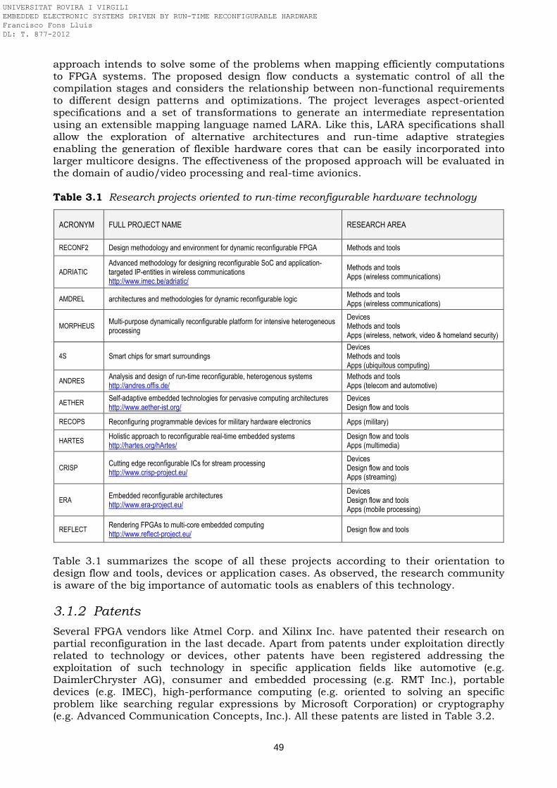
49
approach intends to solve some of the problems when mapping efficiently computations to FPGA systems. The proposed design flow conducts a systematic control of all the compilation stages and considers the relationship between non-functional requirements to different design patterns and optimizations. The project leverages aspect-oriented specifications and a set of transformations to generate an intermediate representation using an extensible mapping language named LARA. Like this, LARA specifications shall allow the exploration of alternative architectures and run-time adaptive strategies enabling the generation of flexible hardware cores that can be easily incorporated into larger multicore designs. The effectiveness of the proposed approach will be evaluated in the domain of audio/video processing and real-time avionics. Table 3.1 Research projects oriented to run-time reconfigurable hardware technology
ACRONYM
FULL PROJECT NAME
RESEARCH AREA
RECONF2 Design methodology and environment for dynamic reconfigurable FPGA Methods and tools
ADRIATIC Advanced methodology for designing reconfigurable SoC and application-targeted IP-entities in wireless communications http://www.imec.be/adriatic/
Methods and tools Apps (wireless communications)
AMDREL architectures and methodologies for dynamic reconfigurable logic Methods and tools Apps (wireless communications)
MORPHEUS Multi-purpose dynamically reconfigurable platform for intensive heterogeneous processing
Devices Methods and tools Apps (wireless, network, video & homeland security)
4S Smart chips for smart surroundings Devices Methods and tools Apps (ubiquitous computing)
ANDRES Analysis and design of run-time reconfigurable, heterogenous systems http://andres.offis.de/
Methods and tools Apps (telecom and automotive)
AETHER Self-adaptive embedded technologies for pervasive computing architectures http://www.aether-ist.org/
Devices Design flow and tools
RECOPS Reconfiguring programmable devices for military hardware electronics Apps (military)
HARTES Holistic approach to reconfigurable real-time embedded systems http://hartes.org/hArtes/
Design flow and tools Apps (multimedia)
CRISP Cutting edge reconfigurable ICs for stream processing http://www.crisp-project.eu/
Devices Design flow and tools Apps (streaming)
ERA Embedded reconfigurable architectures http://www.era-project.eu/
Devices Design flow and tools Apps (mobile processing)
REFLECT
Rendering FPGAs to multi-core embedded computing http://www.reflect-project.eu/
Design flow and tools
Table 3.1 summarizes the scope of all these projects according to their orientation to design flow and tools, devices or application cases. As observed, the research community is aware of the big importance of automatic tools as enablers of this technology.
3.1.2 Patents
Several FPGA vendors like Atmel Corp. and Xilinx Inc. have patented their research on partial reconfiguration in the last decade. Apart from patents under exploitation directly related to technology or devices, other patents have been registered addressing the exploitation of such technology in specific application fields like automotive (e.g. DaimlerChryster AG), consumer and embedded processing (e.g. RMT Inc.), portable devices (e.g. IMEC), high-performance computing (e.g. oriented to solving an specific problem like searching regular expressions by Microsoft Corporation) or cryptography (e.g. Advanced Communication Concepts, Inc.). All these patents are listed in Table 3.2.
UNIVERSITAT ROVIRA I VIRGILI EMBEDDED ELECTRONIC SYSTEMS DRIVEN BY RUN-TIME RECONFIGURABLE HARDWARE Francisco Fons Lluís DL: T. 877-2012
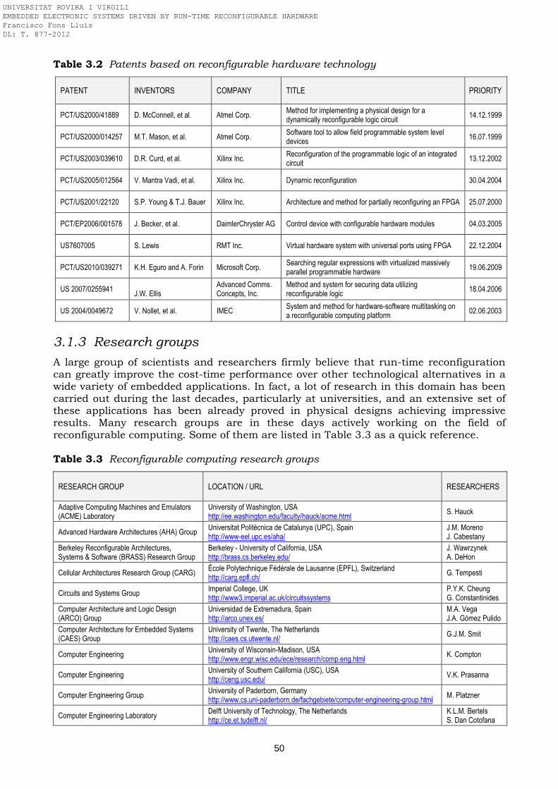
50
Table 3.2 Patents based on reconfigurable hardware technology
PATENT INVENTORS COMPANY TITLE PRIORITY
PCT/US2000/41889 D. McConnell, et al. Atmel Corp. Method for implementing a physical design for a dynamically reconfigurable logic circuit
14.12.1999
PCT/US2000/014257 M.T. Mason, et al. Atmel Corp. Software tool to allow field programmable system level devices
16.07.1999
PCT/US2003/039610 D.R. Curd, et al. Xilinx Inc. Reconfiguration of the programmable logic of an integrated circuit
13.12.2002
PCT/US2005/012564 V. Mantra Vadi, et al. Xilinx Inc. Dynamic reconfiguration 30.04.2004
PCT/US2001/22120 S.P. Young & T.J. Bauer Xilinx Inc. Architecture and method for partially reconfiguring an FPGA 25.07.2000
PCT/EP2006/001578 J. Becker, et al. DaimlerChryster AG Control device with configurable hardware modules 04.03.2005
US7607005 S. Lewis RMT Inc. Virtual hardware system with universal ports using FPGA 22.12.2004
PCT/US2010/039271 K.H. Eguro and A. Forin Microsoft Corp. Searching regular expressions with virtualized massively parallel programmable hardware
19.06.2009
US 2007/0255941 J.W. Ellis
Advanced Comms. Concepts, Inc.
Method and system for securing data utilizing reconfigurable logic
18.04.2006
US 2004/0049672 V. Nollet, et al. IMEC System and method for hardware-software multitasking on a reconfigurable computing platform
02.06.2003
3.1.3 Research groups
A large group of scientists and researchers firmly believe that run-time reconfiguration can greatly improve the cost-time performance over other technological alternatives in a wide variety of embedded applications. In fact, a lot of research in this domain has been carried out during the last decades, particularly at universities, and an extensive set of these applications has been already proved in physical designs achieving impressive results. Many research groups are in these days actively working on the field of reconfigurable computing. Some of them are listed in Table 3.3 as a quick reference. Table 3.3 Reconfigurable computing research groups
RESEARCH GROUP
LOCATION / URL RESEARCHERS
Adaptive Computing Machines and Emulators (ACME) Laboratory
University of Washington, USA http://ee.washington.edu/faculty/hauck/acme.html
S. Hauck
Advanced Hardware Architectures (AHA) Group Universitat Politècnica de Catalunya (UPC), Spain http://www-eel.upc.es/aha/
J.M. Moreno J. Cabestany
Berkeley Reconfigurable Architectures, Systems & Software (BRASS) Research Group
Berkeley - University of California, USA http://brass.cs.berkeley.edu/
J. Wawrzynek A. DeHon
Cellular Architectures Research Group (CARG) École Polytechnique Fédérale de Lausanne (EPFL), Switzerland http://carg.epfl.ch/
G. Tempesti
Circuits and Systems Group Imperial College, UK http://www3.imperial.ac.uk/circuitssystems
P.Y.K. Cheung G. Constantinides
Computer Architecture and Logic Design (ARCO) Group
Universidad de Extremadura, Spain http://arco.unex.es/
M.A. Vega J.A. Gómez Pulido
Computer Architecture for Embedded Systems (CAES) Group
University of Twente, The Netherlands http://caes.cs.utwente.nl/
G.J.M. Smit
Computer Engineering University of Wisconsin-Madison, USA http://www.engr.wisc.edu/ece/research/comp.eng.html
K. Compton
Computer Engineering University of Southern California (USC), USA http://ceng.usc.edu/
V.K. Prasanna
Computer Engineering Group University of Paderborn, Germany http://www.cs.uni-paderborn.de/fachgebiete/computer-engineering-group.html
M. Platzner
Computer Engineering Laboratory Delft University of Technology, The Netherlands http://ce.et.tudelft.nl/
K.L.M. Bertels S. Dan Cotofana
UNIVERSITAT ROVIRA I VIRGILI EMBEDDED ELECTRONIC SYSTEMS DRIVEN BY RUN-TIME RECONFIGURABLE HARDWARE Francisco Fons Lluís DL: T. 877-2012
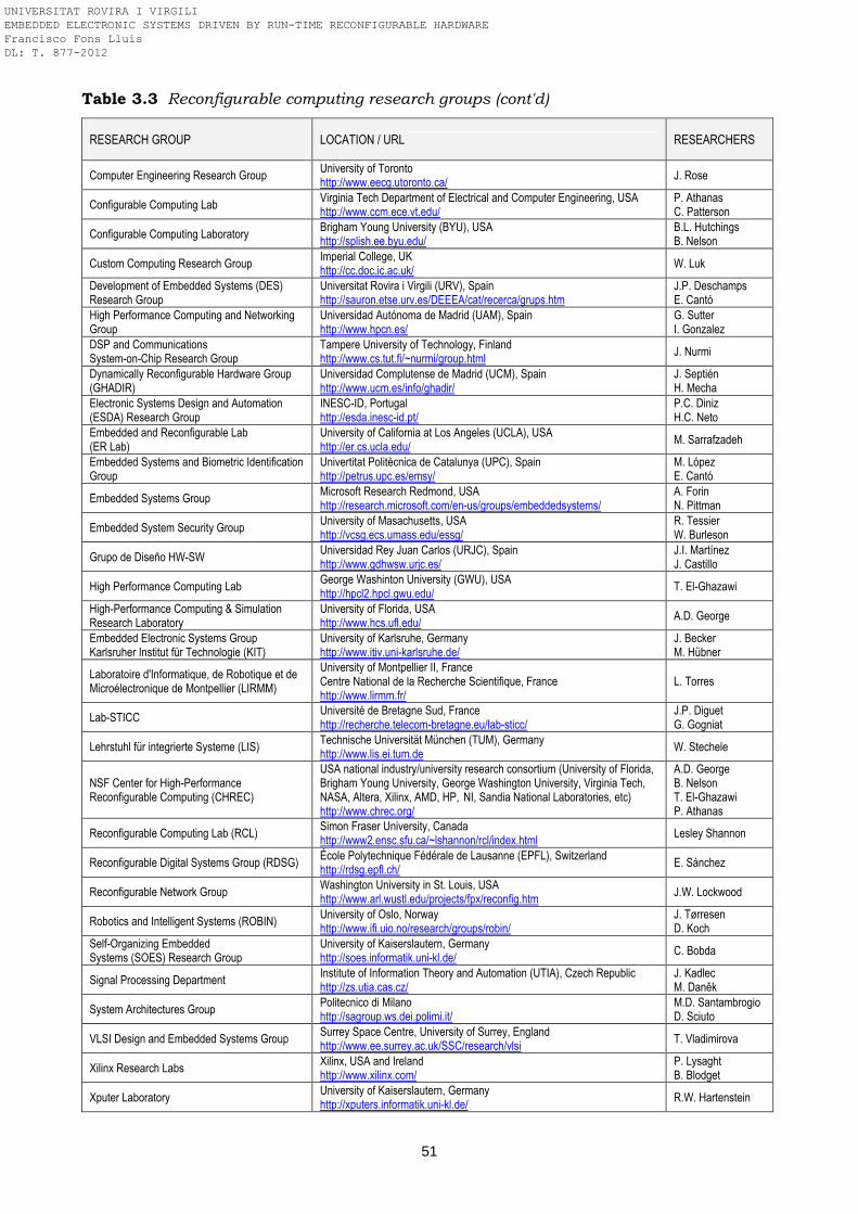
51
Table 3.3 Reconfigurable computing research groups (cont'd)
RESEARCH GROUP
LOCATION / URL RESEARCHERS
Computer Engineering Research Group University of Toronto http://www.eecg.utoronto.ca/
J. Rose
Configurable Computing Lab Virginia Tech Department of Electrical and Computer Engineering, USA http://www.ccm.ece.vt.edu/
P. Athanas C. Patterson
Configurable Computing Laboratory Brigham Young University (BYU), USA http://splish.ee.byu.edu/
B.L. Hutchings B. Nelson
Custom Computing Research Group Imperial College, UK http://cc.doc.ic.ac.uk/
W. Luk
Development of Embedded Systems (DES) Research Group
Universitat Rovira i Virgili (URV), Spain http://sauron.etse.urv.es/DEEEA/cat/recerca/grups.htm
J.P. Deschamps E. Cantó
High Performance Computing and Networking Group
Universidad Autónoma de Madrid (UAM), Spain http://www.hpcn.es/
G. Sutter I. Gonzalez
DSP and Communications System-on-Chip Research Group
Tampere University of Technology, Finland http://www.cs.tut.fi/~nurmi/group.html
J. Nurmi
Dynamically Reconfigurable Hardware Group (GHADIR)
Universidad Complutense de Madrid (UCM), Spain http://www.ucm.es/info/ghadir/
J. Septién H. Mecha
Electronic Systems Design and Automation (ESDA) Research Group
INESC-ID, Portugal http://esda.inesc-id.pt/
P.C. Diniz H.C. Neto
Embedded and Reconfigurable Lab (ER Lab)
University of California at Los Angeles (UCLA), USA http://er.cs.ucla.edu/
M. Sarrafzadeh
Embedded Systems and Biometric Identification Group
Univertitat Politècnica de Catalunya (UPC), Spain http://petrus.upc.es/emsy/
M. López E. Cantó
Embedded Systems Group Microsoft Research Redmond, USA http://research.microsoft.com/en-us/groups/embeddedsystems/
A. Forin N. Pittman
Embedded System Security Group University of Masachusetts, USA http://vcsg.ecs.umass.edu/essg/
R. Tessier W. Burleson
Grupo de Diseño HW-SW Universidad Rey Juan Carlos (URJC), Spain http://www.gdhwsw.urjc.es/
J.I. Martínez J. Castillo
High Performance Computing Lab George Washinton University (GWU), USA http://hpcl2.hpcl.gwu.edu/
T. El-Ghazawi
High-Performance Computing & Simulation Research Laboratory
University of Florida, USA http://www.hcs.ufl.edu/
A.D. George
Embedded Electronic Systems Group Karlsruher Institut für Technologie (KIT)
University of Karlsruhe, Germany http://www.itiv.uni-karlsruhe.de/
J. Becker M. Hübner
Laboratoire d'Informatique, de Robotique et de Microélectronique de Montpellier (LIRMM)
University of Montpellier II, France Centre National de la Recherche Scientifique, France http://www.lirmm.fr/
L. Torres
Lab-STICC Université de Bretagne Sud, France http://recherche.telecom-bretagne.eu/lab-sticc/
J.P. Diguet G. Gogniat
Lehrstuhl für integrierte Systeme (LIS) Technische Universität München (TUM), Germany http://www.lis.ei.tum.de
W. Stechele
NSF Center for High-Performance Reconfigurable Computing (CHREC)
USA national industry/university research consortium (University of Florida, Brigham Young University, George Washington University, Virginia Tech, NASA, Altera, Xilinx, AMD, HP, NI, Sandia National Laboratories, etc) http://www.chrec.org/
A.D. George B. Nelson T. El-Ghazawi P. Athanas
Reconfigurable Computing Lab (RCL) Simon Fraser University, Canada http://www2.ensc.sfu.ca/~lshannon/rcl/index.html
Lesley Shannon
Reconfigurable Digital Systems Group (RDSG) École Polytechnique Fédérale de Lausanne (EPFL), Switzerland http://rdsg.epfl.ch/
E. Sánchez
Reconfigurable Network Group Washington University in St. Louis, USA http://www.arl.wustl.edu/projects/fpx/reconfig.htm
J.W. Lockwood
Robotics and Intelligent Systems (ROBIN) University of Oslo, Norway http://www.ifi.uio.no/research/groups/robin/
J. Tørresen D. Koch
Self-Organizing Embedded Systems (SOES) Research Group
University of Kaiserslautern, Germany http://soes.informatik.uni-kl.de/
C. Bobda
Signal Processing Department Institute of Information Theory and Automation (UTIA), Czech Republic http://zs.utia.cas.cz/
J. Kadlec M. Daněk
System Architectures Group Politecnico di Milano http://sagroup.ws.dei.polimi.it/
M.D. Santambrogio D. Sciuto
VLSI Design and Embedded Systems Group Surrey Space Centre, University of Surrey, England http://www.ee.surrey.ac.uk/SSC/research/vlsi
T. Vladimirova
Xilinx Research Labs Xilinx, USA and Ireland http://www.xilinx.com/
P. Lysaght B. Blodget
Xputer Laboratory University of Kaiserslautern, Germany http://xputers.informatik.uni-kl.de/
R.W. Hartenstein
UNIVERSITAT ROVIRA I VIRGILI EMBEDDED ELECTRONIC SYSTEMS DRIVEN BY RUN-TIME RECONFIGURABLE HARDWARE Francisco Fons Lluís DL: T. 877-2012
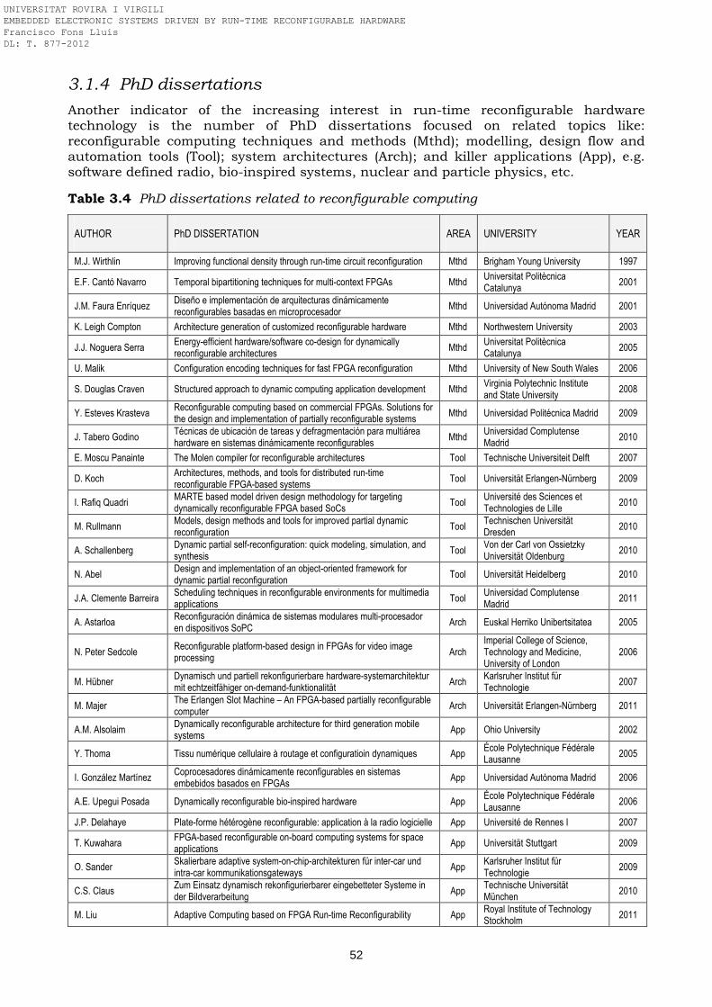
52
3.1.4 PhD dissertations
Another indicator of the increasing interest in run-time reconfigurable hardware technology is the number of PhD dissertations focused on related topics like: reconfigurable computing techniques and methods (Mthd); modelling, design flow and automation tools (Tool); system architectures (Arch); and killer applications (App), e.g. software defined radio, bio-inspired systems, nuclear and particle physics, etc.
Table 3.4 PhD dissertations related to reconfigurable computing
AUTHOR
PhD DISSERTATION
AREA
UNIVERSITY
YEAR
M.J. Wirthlin Improving functional density through run-time circuit reconfiguration Mthd Brigham Young University 1997
E.F. Cantó Navarro Temporal bipartitioning techniques for multi-context FPGAs Mthd Universitat Politècnica Catalunya
2001
J.M. Faura Enríquez Diseño e implementación de arquitecturas dinámicamente reconfigurables basadas en microprocesador
Mthd Universidad Autónoma Madrid 2001
K. Leigh Compton Architecture generation of customized reconfigurable hardware Mthd Northwestern University 2003
J.J. Noguera Serra Energy-efficient hardware/software co-design for dynamically reconfigurable architectures
Mthd Universitat Politècnica Catalunya
2005
U. Malik Configuration encoding techniques for fast FPGA reconfiguration Mthd University of New South Wales 2006
S. Douglas Craven Structured approach to dynamic computing application development Mthd Virginia Polytechnic Institute and State University
2008
Y. Esteves Krasteva Reconfigurable computing based on commercial FPGAs. Solutions for the design and implementation of partially reconfigurable systems
Mthd Universidad Politécnica Madrid 2009
J. Tabero Godino Técnicas de ubicación de tareas y defragmentación para multiárea hardware en sistemas dinámicamente reconfigurables
Mthd Universidad Complutense Madrid
2010
E. Moscu Panainte The Molen compiler for reconfigurable architectures Tool Technische Universiteit Delft 2007
D. Koch Architectures, methods, and tools for distributed run-time reconfigurable FPGA-based systems
Tool Universität Erlangen-Nürnberg 2009
I. Rafiq Quadri MARTE based model driven design methodology for targeting dynamically reconfigurable FPGA based SoCs
Tool Université des Sciences et Technologies de Lille
2010
M. Rullmann Models, design methods and tools for improved partial dynamic reconfiguration
Tool Technischen Universität Dresden
2010
A. Schallenberg Dynamic partial self-reconfiguration: quick modeling, simulation, and synthesis
Tool Von der Carl von Ossietzky Universität Oldenburg
2010
N. Abel Design and implementation of an object-oriented framework for dynamic partial reconfiguration
Tool Universität Heidelberg 2010
J.A. Clemente Barreira Scheduling techniques in reconfigurable environments for multimedia applications
Tool Universidad Complutense Madrid
2011
A. Astarloa Reconfiguración dinámica de sistemas modulares multi-procesador en dispositivos SoPC
Arch Euskal Herriko Unibertsitatea 2005
N. Peter Sedcole Reconfigurable platform-based design in FPGAs for video image processing
Arch Imperial College of Science, Technology and Medicine, University of London
2006
M. Hübner Dynamisch und partiell rekonfigurierbare hardware-systemarchitektur mit echtzeitfähiger on-demand-funktionalität
Arch Karlsruher Institut für Technologie
2007
M. Majer The Erlangen Slot Machine – An FPGA-based partially reconfigurable computer
Arch Universität Erlangen-Nürnberg 2011
A.M. Alsolaim Dynamically reconfigurable architecture for third generation mobile systems
App Ohio University 2002
Y. Thoma Tissu numérique cellulaire à routage et configuratioin dynamiques App École Polytechnique Fédérale Lausanne
2005
I. González Martínez Coprocesadores dinámicamente reconfigurables en sistemas embebidos basados en FPGAs
App Universidad Autónoma Madrid 2006
A.E. Upegui Posada Dynamically reconfigurable bio-inspired hardware App École Polytechnique Fédérale Lausanne
2006
J.P. Delahaye Plate-forme hétérogène reconfigurable: application à la radio logicielle App Université de Rennes I 2007
T. Kuwahara FPGA-based reconfigurable on-board computing systems for space applications
App Universität Stuttgart 2009
O. Sander Skalierbare adaptive system-on-chip-architekturen für inter-car und intra-car kommunikationsgateways
App Karlsruher Institut für Technologie
2009
C.S. Claus Zum Einsatz dynamisch rekonfigurierbarer eingebetteter Systeme in der Bildverarbeitung
App Technische Universität München
2010
M. Liu Adaptive Computing based on FPGA Run-time Reconfigurability App Royal Institute of Technology Stockholm
2011
UNIVERSITAT ROVIRA I VIRGILI EMBEDDED ELECTRONIC SYSTEMS DRIVEN BY RUN-TIME RECONFIGURABLE HARDWARE Francisco Fons Lluís DL: T. 877-2012
53
3.2 Reconfigurable hardware devices
Next, it is presented the state-of-the-art about commercial and research devices that exploit reconfigurable computing technology. The list of devices is split in two categories: commercial/industrial devices and academic/research platforms.
3.2.1 Commercial and industrial FPGAs and SoCs
Nowadays, programmable logic is one of the fastest growing segments of the entire semiconductor market. The programmable logic industry is controlled today by several established FPGA vendors, mainly Xilinx, Altera, Actel/Microsemi, Lattice and Atmel. Besides, some coarse-grained devices from other companies like PACT XPP Technologies or Recore Systems are commercially available. Although there are several programmable logic manufacturers distributing their products, only few of these devices present in the market support run-time reconfigurable computing. A brief description of these devices is presented next, specially focusing on the reconfigurable hardware aspects of each family. A. Altera (www.altera.com)
Altera is focused on FPGA devices based on SRAM programming technology. It distinguishes three types of products: high-end devices (Stratix, Stratix-II, Stratix-III, Stratix-IV and Stratix-V series), mid-range devices (Arria GX, Arria II and Arria V series) and low-cost devices (Cyclone, Cyclone-II, Cyclone-III, Cyclone-IV and Cyclone-V families). Although most of the Altera FPGA devices are not equipped with partial reconfiguration features, Altera Corp. announced the introduction, by first time in their devices, of partial reconfiguration in the new 28-nm versions of their FPGA families, Stratix-V, Arria-V and Cyclone-V devices. In this way, Altera has joined the group of FPGA manufacturers that provide devices supporting run-time partial reconfiguration technology. Regarding SoPC devices, Altera developed the Excalibur family in the early 2000s, although today is already not shipped. The Excalibur device is composed of a microprocessor subsystem and FPGA configuration logic. The microprocessor subsystem (or embedded stripe) includes a 32-bit ARM922T processor with AMBA advanced high-performance bus (AHB) bus structure, SRAM and dual-port SRAM memories, Flash, SRAM, and SDRAM interfaces, and peripherals. The programmable logic of Excalibur is composed by the equivalent resources of an Altera APEX20KE FPGA. Unlike FPGA solutions, Excalibur devices can be reconfigured at any time via processor control, while the processor continues to run. This architecture lets deploy run-time reconfigurable hardware applicatioin with this device. More recently, just in 28-nm Arria-V and Cyclone-V devices, Altera is including a hard dual-core processor together with programmable logic giving rise to SoC FPGAs. These devices feature a hard processor system containing a dual-core ARM Cortex-A9 MPCore processor and a rich set of peripherals seamlessly linked to the FPGA fabric. Once running, the hard processor system can fully or partially reconfigure the FPGA fabric at any time under software control. Concerning tools, Altera integrates the PR flow in its Quartus-II tools. B. Atmel (www.atmel.com)
Atmel has developed several SRAM-based FPGA devices like the mature AT6000 family and the AT40K family. These devices, although they are small in capacity, are equipped with fine grain reconfigurability. New devices currently under development are the radiation hardened ATF280E and ATFS450 devices oriented to aerospace applications, in addition to the rad-hard version of the AT40K named AT40FEL. Apart from FPGA devices, Atmel has developed the AT94K SoC family, also called Field-Programmable System-Level Integrated Circuit (FPSLIC), composed of a hard-core AVR processor and an AT40K FPGA, both from Atmel, inside the same chip. Besides, a secure version of FPSLIC, the AT94S device, furthermore integrates non-volatile memory inside the chip.
UNIVERSITAT ROVIRA I VIRGILI EMBEDDED ELECTRONIC SYSTEMS DRIVEN BY RUN-TIME RECONFIGURABLE HARDWARE Francisco Fons Lluís DL: T. 877-2012
54
Regarding dynamic reconfiguration, both FPGAs and SoCs are equipped with Cache Logic technology, which corresponds to fine-grain run-time partial reconfiguration developed by Atmel. Concerning automatic tools, the Atmel Figaro tool is currently in use to develop reconfigurable hardware applications with Atmel FPGAs. C. Lattice (www.latticesemi.com)
Lattice Semiconductor produces different families of FPGAs suitable for general-purpose applications: Lattice EC, ECP, ECP2, ECP2M, ECP3, ispXPGA, SC, SCM, XP and XP2. In general, the Lattice FPGA architecture is composed of a grid of logic blocks which contain SRAM-based resources for logic, arithmetic and RAM blocks, and also non-volatile Flash memory blocks. The SRAM contains the working configuration whereas the Flash memory retains the configuration for use as necessary. Moreover, the contents of the Flash memory can be loaded into SRAM automatically at power-up or at any desired time, replacing the need for external boot memory and enabling thus a single-chip solution. The more relevant reconfigurability feature of the Lattice FPGA devices is the so-called Transparent Field Reconfiguration (TransFR). TransFR I/O is a technology that allows users to update their logic in the field without interrupting the system operation. TransFR I/O allows I/O states to be frozen during device configuration. This allows the device to be field updated with a minimum of system disruption and downtime, being completely transparent to the application. The process consists of four phases: backgroung programming – through which the NVM (internal or external) is reprogrammed while the RAM is running undisturbed; boundary scan locks outputs, where I/O states are captured and held or driven to a user-defined level using JTAG commands; device configuration by transferring the new functionality from non-volatile memory to SRAM configuration space; and boundary scan released so that the internal logic reassumes control of the I/Os. D. Xilinx (www.xilinx.com)
Xilinx is undoubtedly the FPGA manufacturer which has bet the most on dynamic partial reconfiguration technology. Recognizing that it is no longer sufficient to just build an ever-larger FPGA, Xilinx has put the spotlight on the partial reconfiguration capabilities of its devices as a powerful weapon in the competitive landscape and, more importantly, it has dedicated the resources and support to make partial reconfiguration an equally powerful capability for users. The first Xilinx FPGA family provided with dynamic partial reconfiguration capability was the XC6200 series. It is the first commercial FPGA to address the requirements of interfacing programmable logic to microprocessors. Like this, it is provided with a full parallel (configurable as 8, 16 or 32 bits in width) CPU interface referred to as FastMap and managed by chip select and read/write control signals. This makes the configuration SRAM and logic cells appear as conventional memory mapped SRAM, and the configuration file consists of a set of address/data pairs, allowing fine grain reconfiguration of individual words, bytes or even single bits in real-time. Fast reconfiguration of the entire chip can be performed in less than 200 microseconds. Additionally, the ability to partially reconfigure the device even more rapidly is also supported, which increases application flexibility: up to 32 bits can be reconfigured in approximately 40 nanoseconds. Thus, in 1996 the first generation of PR was born with the XC6200 series of FPGAs, although today they are already discontinued and Xilinx ceased their shipment. In 1999, it is launched the second generation of PR, applied this time to Xilinx Virtex devices first and, along the time, extended also to Virtex-II and Virtex-II Pro devices. At that date, PR was seen only as a promising disruptive technology but not fully supported by tools to drive the development of professional applications and products. Unlike XC6200 devices, in Virtex FPGAs the configuration memory is segmented into frames. In fact, the organization of the configuration memory is strongly influenced by the FPGA internal configuration control logic and, in the first Virtex families, each configuration frame encompasses the
UNIVERSITAT ROVIRA I VIRGILI EMBEDDED ELECTRONIC SYSTEMS DRIVEN BY RUN-TIME RECONFIGURABLE HARDWARE Francisco Fons Lluís DL: T. 877-2012
55
implementation of a column of resources in the FPGA logic. A configuration frame is the smallest unit of data which can be accessed in a single reconfiguration cycle, consisting typically of some hundreds of bytes. The exact amount of data in a configuration frame depends on the device itself. For instance, in Virtex-II, the column of logic resources governed by a configuration frame spans the full height of the device. Consequently, frames for shorter devices contain fewer data than frames for taller devices. Concerning the reconfiguration controller, all Virtex devices make use of the SelectMap and ICAP (internal configuration access port) interfaces. In parallel to the high-end Virtex family (Virtex, Virtex-E, Virtex-II, Virtex-II Pro, Virtex-4, Virtex-5, Virtex-6 and Virtex-7), Xilinx has also developed a low-end family (Spartan, Spartan-3, Spartan-3E, Spartan-3A/3A DSP/3AN, Spartan-6) that differs from the PR point of view in the fact that it is not built with PR glitchless technology (except Spartan-6). Nevertheless, although these devices have never been officially supported by the Xilinx PR design flow, partial reconfiguration is possible and some proofs have been successfully performed by several research groups in the community. In 2006, Xilinx releases the third generation of PR based on a modular design flow. With this, it is problably reached the first mature level of partial reconfiguration technology, this time applied to Virtex-4 and Virtex-5 devices. This new PR design flow already lets the designer follow all the development steps in a quite automatic and consistent way to reach a PR application. Furthermore, Virtex-4 and Virtex-5 devices did a decisive step forward concerning partial reconfiguration. As example, the configuration frames of the Xilinx Virtex-4 series have a single fixed size, with a smaller reconfiguration granularity of 16 CLBs high. Therefore, these devices do not have the reconfiguration constraint of spanning the full height of the FPGA like in the previous Virtex-II devices. This allows designers to have finer granularity and more control over the resources in the FPGA they are reconfiguring. Moreover, the reconfiguration engine is notoriously improved and the reconfiguration bandwidth increases in comparison to their predecessors, allowing a maximum reconfiguration rate of 3.2 Gbps for whatever partial bitstream. At the same time, in the aerospace field, Xilinx has been working in rad-hard reconfigurable versions of Virtex-4 and Virtex-5 FPGAs clearly oriented to space applications, like Virtex-4QV and Virtex-5QV families. The PR modular flow of 2006 achievement definitely meant a turning point concerning the potential of PR technology. From that moment on, new improvements have been adopted. In 2009-2010, Xilinx works on a new design flow oriented to PR partitions and extended to Virtex-6 devices. This PR design flow becomes the fourth generation of Xilinx partial reconfiguration and is integrated as mainstream in the ISE 12 tool, giving open access to PR to any FPGA design team. Recently, in 2011 Xilinx presented the fifth generation of PR devices composed of the 7-series FPGAs built in 28-nm technology and holding partial reconfiguration in their Virtex-7, Kintex-7 and Artix-7 families. In parallel, Xilinx launches the Zynq-7000 Extensible Processing Platform (EPP), a family of SoC devices which tightly combine a complete ARM dual-core Cortex-A9 MPCore processor with integrated 28-nm Xilinx’s Artix-7 or Kintex-7 equivalent programmable logic wich can be partially reconfigurable at run-time. Besides, the ISE 13 PR design flow with enhanced usability is launched, becoming the fifth generation of PR addressed to Virtex-6 and 7-series FPGAs and it is announced the ISE 14 extended to the Zynq-7000 family. Xilinx delivers a complete toolset to support all the design flow: ISE and PlanAhead for the synthesis and hardware, System Generator for digital signal processing, EDK and SDK for dealing with software implementation, and Chipscope for debugging purposes. Other third-party tools like Matlab/simulink, for implementing DSP designs convertible to RTL code, or AutoESL, which lets translate algorithms programmed in C/C++ to RTL, are further alternatives that are gaining popularity today. E. Others
Many other companies and startups have shown their interest in programmable logic and run-time reconfigurable hardware technology:
UNIVERSITAT ROVIRA I VIRGILI EMBEDDED ELECTRONIC SYSTEMS DRIVEN BY RUN-TIME RECONFIGURABLE HARDWARE Francisco Fons Lluís DL: T. 877-2012
56
Tabula (www.tabula.com) Tabula Inc., a programmable logic startup, released its new family of programmable logic devices ABAX currently in volume production provided with up to 8 different hardware contexts or stacked layers (folds) that can be swapped on the fly in some few picoseconds. In these devices, each fold performs a portion of the desired function and stores the result in place. When some or all of a fold is reconfigured, it uses the locally stored data to perform the next portion of the function. By rapidly reconfiguring to execute different portions of each function, the device can implement a complex design using only a small fraction of the resources that would be required by a static hardware design, and performing the reconfiguration at GHz rates.
PACT XPP Technologies (www.pactxpp.com) PACT XPP Technologies is a company oriented to multimedia communication server accelerator solutions which has developed the XPP (eXtreme Processing Platform) architecture. This architecture is present in the commercially available XPP-III processors, a heterogenous multicore architecture provided by two basic types of processing resources to combine sequential and parallel data processing: a set of unique cores –function processing array elements or PAEs– are dedicated to strictly sequential tasks and a reconfigurable array –the XPP array– takes care of data streams. Thus, the function PAEs process sequential tasks, like operating system, protocol stacks and decoding, whereas the XPP array directly processes high bandwidth data streams, such as pixel and audio. Moreover, concerning reconfiguration capability, ultra fast array reconfiguration allows on-the-fly exchange of processing tasks executed on the array.
Recore Systems (www.recoresystems.com) Recore Systems is a fabless semiconductor company that develops advanced digital signal processing platform chips and licenses reconfigurable semiconductor IP. The company is specialized in reconfigurable multicore designs that allow instant adaptation to new situations and offer a unique combination of flexibility, high performance, low power and low cost by means of merging in a same fabric heterogeneous processing elements to match thus the granularity of whatever synthesizable algorithm or application with the granularity of the hardware inside the device. Recore Systems has developed two types of dynamically reconfigurable cores: Montium and Xentium. The reconfigurable Montium processor consists of a Processing Part Array (PPA) and a Communication and Control Unit (CCU) and its reconfiguration typically takes less than 5 µs using a 100 MHz clock. The Xentium processor is a fixed point VLIW-DSP core designed for high-performance embedded signal processing with an instruction set optimized for digital baseband processing.
Menta (www.menta.fr) Menta is an FPGA startup specifically focused on embedded FPGAs (eFPGAs) which, in collaboration with the Laboratory of Informatics, Robotics and Microelectronics of Montpellier (LIRMM) have developed the world’s first FPGA built in non-volatile magnetoresistive random access memory (MRAM), claiming that this technology proposes better non-volatile configuration versatility, dynamic partial reconfiguration capabilities and instantaneous on/off total or partial energy savings than SRAM and Flash technologiies. Besides its advantage against Flash-based FPGA technology in power saving during standby mode, it also benefits the access speed of SRAM but with configuration time reduction since there is no need to load the configuration data from an external non-volatile memory as in SRAM-based FPGAs. Furthermore, during the FPGA circuit operation, the magnetic tunneling junctions can be written, which allows a dynamic configuration (both partial and multicontext reconfiguration) and increases the flexibility and performance of FPGA circuits [Guillemenet et al., IJRC 2008]. Further programmable logic startups interested in run-time reconfigurable hardware have disappeared, as listed next in summarized form:
UNIVERSITAT ROVIRA I VIRGILI EMBEDDED ELECTRONIC SYSTEMS DRIVEN BY RUN-TIME RECONFIGURABLE HARDWARE Francisco Fons Lluís DL: T. 877-2012
57
SIDSA, which developed the SoC called FIPSOC (abbreviation of Field Programmable System-On-Chip) provided with an 8051 MCU, configurable analog blocks and programmable logic with excellent multi-context full and partial dynamic reconfiguration capabilities in a single substrate. Although already out of production, the more relevant feature of FIPSOC is its multi-context dynamic reconfiguration capability: chip configuration is stored in static RAM bits and either the microprocessor or the logic circuit itself can drive a context update of the complete sea of cells or only a square region. The configuration data is loaded to the active memory context by issuing a memory write command and while the cell is in operation according to the data stored in the configuration bits one or two new contexts can be pre-loaded on the backup memory. This feature enables multi-context dynamic reconfiguration since there is no need to stop the chip to reconfigure it as these two extra configurations can be swapped in real-time.
Chameleon Systems, a fabless semiconductor company which developed the CS2000 family of reconfigurable communications processors. Each product in the CS2000 family has main functional blocks like a 32-bit RISC processor and a reconfigurable processing fabric, interconnected through a high-speed system bus. The reconfigurable processing fabric comprises an array of reconfigurable tiles used to implement the desired application algorithms and organized in slices. Moreover, loading the background plane from external memory requires 3 microseconds per slice and such operation does not interfere with active processing on the fabric. Afterwards, powered by the company's proprietary eConfigurable technology, swapping the background plane into the active plane requires only one clock cycle, that is, the entire reconfigurable processing fabric can be changed from one algorithm to another in a single clock cycle.
National Semiconductor, which developed the SRAM-based partially reconfigurable FPGA device called Configurable Logic Array (CLAy).
Some other startups have been absorbed by other FPGA companies, like Algotronix, which developed the CAL SRAM-based FPGA supporting PR and was acquired by Xilinx.
3.2.2 Research and academic reconfigurable platforms
Along the time, many research groups have developed their own hardware platforms to carry out their investigation on reconfigurable computing. Some of these works conducted by research and academic groups have led to the founding of new programmable logic startups delivering commercial devices today, like the Montium core from Recore Systems, result of the research performed by the University of Twente developing a tiled heterogeneous SoC so-called Chameleon, or the FIPSOC device from SIDSA, developed in part by the Universitat Politècnica de Catatunya. Many other reconfigurable hardware platforms emerged from the academia are discussed next. Unlike the fine-grained reconfigurable devices from FPGA vendors overviewed in the previous section, most of the platforms presented here are coarse-grained architectures. The two approaches are complementary: coarse-grained architectures are typically used for acceleration of algorithms that have a high level of data-intensive processing but exhibit less control flow and fine-grained approaches in contrast are preferred for mapping of algorithms with increased amount of control flow by synthesizing instructions. Most coarse-grained architectures are moreover coupled with RISC processors to execute entire applications. This section reviews some of the most popular architectures experimented in reconfigurable computing by the research community. A. POEtic
The development of systems inspired by biological mechanisms is finding increasing interest in computer science and engineering fields. However, the implementation of bio-inspired systems in silicon is quite difficult due to the high complexity of the biological
UNIVERSITAT ROVIRA I VIRGILI EMBEDDED ELECTRONIC SYSTEMS DRIVEN BY RUN-TIME RECONFIGURABLE HARDWARE Francisco Fons Lluís DL: T. 877-2012
58
mechanisms involved. In this line, POEtic is a SoC conceived to address the prototyping of bio-inspired applications organized around a 32-bit RISC microprocessor and an FPGA composed of a scalable architecture [Moreno et al., ICES 2005]. The flexible hardware substrate of the device is provided with key features which provide capabilities similar to those present in living beings like evolution, development, self-replication, self-repair and learning. Among the more relevant features are the facility to create, dynamically, data paths across resources on one or multiple chips (i.e., dynamic routing), and the ability of both the dedicated microprocessor and the array itself to reconfigure parts of the device (i.e., partial dynamic self-reconfiguration). The POEtic project has been developed by the University of York, École Polytecnique Fédérale de Lausanne, University of Lausanne, Universitat Politècnica de Catalunya and University of Glasgow. B. Chimaera
Chimaera is a micro-architecture which integrates a small and fast reconfigurable functional unit (RFU) into the pipeline of a dynamically-scheduled superscalar processor. This RFU is an FPGA-like logic comprised of cells arranged in rows and designed to implement application specific operations. The applicacion code is split in instructions. Each of these instructions is known as an RFU operation (RFUOP) and corresponds to a RFU configuration executed through a call to the RFU. These RFU calls are handled by the compiler to tell the processor to execute an RFUOP. Hence, Chimaera treats the reconfigurable logic as a cache of RFU instructions, retaining those instructions necessary for the current execution. In this way, the RFU calls act just like any other instruction, fitting into the processor’s standard execution pipeline. If the requested instruction is not currently loaded into the RFU, the host processor is stalled while the RFU fetches the instruction from memory and it is brought into the RFU by reconfiguring itself, either placing it on free space if available, or, otherwise, overwriting one or more of the currently loaded instructions. This does require that the reconfigurable logic be somewhat symmetric, so that a given instruction can be placed into the RFU wherever there is available logic. Like this, the system uses partial run-time reconfiguration to manage the reconfigurable logic and initialize the hardware to perform the specific instruction by loading the configuration bitstream of such instruction into the RFU. The configurations themselves are row-based, with each configuration using as many complete rows as necessary. Thus, every time a new instruction needs to be loaded into the RFU it only changes the contiguous set of rows required to hold that new instruction (http://www.ee.washington.edu/faculty/hauck/chimaera.html). C. ADRES
IMEC (Interuniversitair Microelektronica Centrum) developed the coarse-grained architecture ADRES (Architecture for Dynamically Reconfigurable Embedded Systems) consisting of two tightly coupled parts: a VLIW processor and a coarse-grained reconfigurable matrix. Both parts work according to a processor/coprocessor execution model: the identified compute-intensive processing loops are mapped onto the reconfigurable array whereas the VLIW processor performs the control of the application flow, being both processor and coprocessor coupled through a shared central register file. Concerning reconfiguration features, the configuration memory can store a number of contexts locally in each cell. Thus, a cell may use one or more contexts depending on the functionality implemented. When a specific processing loop is executed in the reconfigurable matrix, these contexts are cyclically loaded until the loop ends. Such architecture template can be synthesized as an application-specific instruction-set processor (ASIP) and it results in a power-efficient and flexible solution oriented to embedded multimedia devices. The ADRES architecture is supported by a compiler framework, DRESC (Dynamically Reconfigurable Embedded System Compiler), which manages all the design flow –mainly compiler, assembler, linker and RTL generators– to map an application written in C onto an ADRES instance [Mei et al., FPL 2003].
UNIVERSITAT ROVIRA I VIRGILI EMBEDDED ELECTRONIC SYSTEMS DRIVEN BY RUN-TIME RECONFIGURABLE HARDWARE Francisco Fons Lluís DL: T. 877-2012
59
D. DISC
Researchers from the Brigham Young University developed a computer named DISC (Dynamic Instruction Set Computer) which lets the user synthesize its own application-specific instruction set. This platform provides application-specific performance to a simple processor by allowing user-defined application-specific instructions to supplement a conventional instruction set. Conceptually, DISC is composed of a host processor, several partially reconfigurable CLAy31 FPGAs from National Semiconductor and external memory. DISC treats instructions as removable modules paged in and out through partial reconfiguration as demanded by the executing program. In this way, the DISC processor uses run-time reconfiguration to provide an essentially limitless application-specific instruction set, where each instruction is implemented as an independent circuit module. An application running on DISC contains source code and a library of application-specific instruction circuit modules. This library is available simply by referencing them as source code in a C program: instruction modules are implemented as partial configurations and individually configured on DISC as demanded by the application program. The ability to replace instruction modules in the system at run-time provided by the partial reconfiguration allows the implementation of an instruction set much larger than is possible on a single static FPGA. Instructions occupy FPGA resources only when needed and FPGA resources can be reused to implement an arbitrary number of custom-made instructions. Nonetheless, the processor needs to be equipped with a relocatable hardware strategy. This relocatable hardware algorithm provides the ability to make placement decisions of partial reconfigurations on the fly. This feature is achieved by designing each custom instruction module for multiple locations on the FPGA and physically independent from each other of the set of instruction modules in the library [Wirthlin and Hutchings, FCCM 1995]. E. DPGA
Dynamically Programmable Gate Arrays (DPGAs) differ from traditional single context FPGAs by providing on-chip memory for multiple array contexts. The configuration memory resources are replicated to contain several configurations for the fixed computing and interconnect resources. In effect, the DPGA contains an on-chip cache of array configurations and exploits high, local on-chip bandwidth to allow reconfiguration to occur rapidly, although loading a new configuration from off-chip is still limited by low off-chip bandwidth. The multiple contexts on the DPGA allow the array to operate on one context while other contexts are being reloaded from off-chip. The DPGA uses traditional 4-input LUTs for the basic array element and interconnect programming cells with a 4-context memory implemented using a 4x32-bit primitive of dynamic RAM. Dynamic reconfiguration between contexts, known as context switching, is controlled through a global instruction signal, thus all array elements switch together: a single 2-bit global context identifier is distributed throughout the array to select the configuration for use among the four possible. Furthermore, an array element in a context has the ability to communicate with the same array element in the following context via its flip-flop. This is because the flip-flop state is not affected by the context switch, thus the flip-flop value is stored between contexts. In summary, the DPGA serves as a multiple-context FPGA which, once the contexts are preloaded, can switch from one context to another in one clock cycle to process an application. As result, the multiple loaded contexts allow using the array elements more efficiently [Tau et al., FPD 1995]. F. Time-multiplexed FPGA
The Time-Multiplexed FPGA (TM-FPGA) is an extension of the Xilinx XC4000E FPGA that exploits some architectural changes to convert it in a multi-context device. Thus, the TM-FPGA maintains the same basic 2D array of CLBs as well as the routing structure of the XC4000E device. However, as novelty, each one of its configuration elements (associated
UNIVERSITAT ROVIRA I VIRGILI EMBEDDED ELECTRONIC SYSTEMS DRIVEN BY RUN-TIME RECONFIGURABLE HARDWARE Francisco Fons Lluís DL: T. 877-2012

60
with either logic or routing bits) is replicated eight times in total by SRAM memory cells. The configuration memory is thus distributed throughout the die, with each active configuration memory cell backed by eight inactive bits stored in the configuration SRAM. This distributed inactive memory can be viewed as eight configuration memory planes or contexts so that the device is composed by one active context, in foreground, and other eight as spare, in background. Each plane is a very large word of memory and the entire reconfiguration of the FPGA can be performed in only one single cycle of the memory; all bits in the logic and interconnect array are updated simultaneously from the on-chip memory in 30ns. Moreover, in order to store signals between contexts, the device incorporates the addition of eight micro registers at the outputs of the CLBs in accordance with the eight configuration memory planes of the device. Each CLB output, either the combinational or sequential output, can be stored in any of the n micro registers. This allows a signal to be stored into a micro register in one context and retrieved in another context, and still allows the operation of the CLB in intermediate contexts. Thus, direct communication between any two contexts is possible. These two architectural changes in the original XC4000E FPGA –configurable bits replication and addition of micro-registers– make feasible the fact that configuration memory planes can be loaded from off-chip while the FPGA is operating [Trimberger et al., FCCM 1997]. G. Garp
The Garp architecture, developed at the University of California, combines a standard MIPS processor with additional reconfigurable hardware on the same die. This hybrid architecture was intended to improve the performance of general-purpose applications split in a main processor and a reconfigurable slave coprocessor tailored specifically for accelerating execution loops of code. The main thread of control through a program is managed by the processor while for certain loops or subroutines are performed by the reconfigurable coprocessor to speed up the processing. Like an FPGA, the Garp array is a two-dimensional array of CLBs interconnected by programmable wiring. It functions as a reconfigurable data path. Besides, memory buses provide a high bandwidth reconfiguration path between the array and the memory. From a reconfiguration viewpoint, this device is rows-oriented, that is, a partial reconfiguration is possible provided that the area reconfigured covers some number of complete and contiguous rows, being one row the smallest configuration grain. Furthermore, distributed with the array is a cache of recently used configurations so that programs can quickly switch between several configurations without the cost of reloading them from memory each time. Together with the Garp architecture, a big effort was done to design a compiler adapted to this architecture. The Garp compiler takes standard ANSI C as input, identifies the pieces of source code, and breaks up the program into basic blocks divided in instruction sequences with no branches which result beneficial –in terms of acceleration– to be executed on the reconfigurable array, and execute everything else on the main processor. Several instructions were added to the MIPS-II instruction set for this purpose, giving thus rise to an instruction set extended for Garp machines ready to manage the coprocessor’s reconfigurations [Callahan et al., Computer 2002]. H. PipeRench
For many applications, a customized data path with appropriate levels of parallelism and pipelining is intrinsically more efficient than traditional software execution. However, an impediment to the use of custom hardware technologies is the cost of developing and reusing such hardware pipelines. The PipeRench architecture, designed at the Carnegie Mellon University (CMU), addresses these problems by introducing a virtual hardware abstraction. This virtualization of hardware is accomplished by run-time reconfiguration of the programmable hardware fabric. Unlike other run-time reconfigurable devices, PipeRench manages its own reconfiguration without any host or user interaction. PipeRench can be looked at as a reconfigurable fabric, i.e., an interconnected parallel-
UNIVERSITAT ROVIRA I VIRGILI EMBEDDED ELECTRONIC SYSTEMS DRIVEN BY RUN-TIME RECONFIGURABLE HARDWARE Francisco Fons Lluís DL: T. 877-2012
61
processing network of logic and storage processing elements. Combined with an off-chip general-purpose processor, PipeRench can support a system in its various computing needs. It is particularly suitable for stream-based media applications or any applications that rely on simple, regular computations on large sets of small data elements [Goldstein et al., Computer 2000]. Thus, using the pipeline reconfiguration technique presented in section 2.3.3.F, PipeRench improves reconfiguration time and saves area by virtualizing pipelined computations. The hardware virtualization is achieved by structuring the configurations into pipeline stages that are time-multiplexed onto the physical stages, breaking a single static configuration into pieces that correspond to pipeline stages in the application. Each pipeline stage is loaded, one per cycle, into the fabric. This makes performing the computation possible, even if the entire configuration is never present in the fabric at one time. But virtualization through pipelined reconfiguration imposes some constraints: it requires that every physical stage be identical and also restricts the computations it can support to those in which the state in any pipeline stage is a function of the current state of that stage and the state of the previous stage in the pipeline – in other words, the dataflow graph of the computation cannot have long cycles. PipeRench was designed at CMU and fabricated by ST Microelectronics in a six-metal layer 0.18 micron CMOS process [Schmit et al., CICC 2002]. I. PRISM
In the mid-90s, researchers from the Brown University developed a computer architecture called PRISM (Processor Reconfiguration through Instruction Set Metamorphosis) consisting of a general-purpose core processor and a reconfigurable FPGA platform designed to bridge the gap between general-purpose and specialized computing. PRISM-I becomes a first proof-of-concept developed to demonstrate the viability of speeding up computationally intensive tasks by extending the core processor’s functionality with new instructions executed on dedicated reconfigurable hardware and tailored specifically for each application [Athanas and Silverman, Computer 1993]. The PRISM-I prototype consists of a Motorola M68010 processor and a reconfigurable platform composed of four Xilinx XC3090 FPGAs. The FPGAs are dynamically configured to execute the critical sections of a given C program more efficiently while the less frequently accessed sections are executed by the core processor. A second research loop on the PRISM approach gives place to PRISM-II. Basically, PRISM-II introduces a novel execution model and a framework for translating a C function into a FPGA-based custom architecture. Furthermore, PRISM-II addresses some hardware and software deficiencies of PRISM-I, like the development of a new system level architecture that improves the communication efficiency between the reconfigurable hardware and the host processor. PRISM-II consists of an AMD AM29050 RISC processor and a reconfigurable platform composed of a set of three Xilinx XC4010 FPGAs [Agarwal et al., ICPP 1994]. In summary, this work carried out at the Brown University presents an architecture and high-level language compiler oriented to improve the execution performance of many applications adapting the configuration and fundamental operations of a core processing system to the computationally intensive portions of a targeted application. J. Others
Many other devices have arised along the time from the research community exploiting run-time reconfiguration features: MorphoSys, DReAM, RaPiD, XPUTER, DECPeRLe-1, SPLASH-2, ARDOISE, SCORE, RAW, NAPA, MATRIX, ONECHIP, KressArrays, etc.
3.3 Summary
The emergence of SRAM-based FPGAs boosted reconfigurable computing as a research and engineering field. While standard MCUs are nowadays the dominant hardware platform in many embedded fields, the decreasing cost of new FPGAs, along with the fact
UNIVERSITAT ROVIRA I VIRGILI EMBEDDED ELECTRONIC SYSTEMS DRIVEN BY RUN-TIME RECONFIGURABLE HARDWARE Francisco Fons Lluís DL: T. 877-2012
62
that some of them harbor hard-core processors inside, makes these devices interesting to be considered for a massive deployment in many embedded application areas. Hence, many indicators show the good health of reconfigurable hardware technology today. Leaded by a growing research community composed mainly by staff from the academia but also from the industry (e.g. programmable logic manufacturers), this field is expanding its application areas through new research projects focused on concepts, physical devices and tools, or even through patents under exploitation in the industry. The broad community of research groups around the world and the continuous proliferation of these groups with new of PhD candidates focused on these areas, ensures the continuity of the task force in this research field. As a result, numerous reconfigurable hardware architectures have been proposed and developed as application/domain specific hardware accelerators, divided basically in two categories: those that target coarse, loop-level optimisations and those that target fine-grain, instruction-level optimisations. In addition, a big effort is addressed to the definition of an efficient ecosystem composed of appropriate automatic tools to manage these reconfigurable architectures and make easier and faster their design flow. Recently, relevant advances have been performed in this direction concerning PR flow and EDA tools pushed by Xilinx. To sum up all these advances, this chapter makes evident the fact that the scientific community is involved in run-time reconfigurable hardware, spending big research efforts from long time ago and showing a great interest in this technology which is expected to continue, as foreseen in part through the funded international research projects that have started to walk recently on this field.
References
[Agarwal et al., ICPP 1994] L. Agarwal, M. Wazlowski, S. Ghosh, An asynchronous approach to synthesizing custom architectures for efficient execution of programs on FPGAs, Proc. Int. Conf. on Parallel Processing, pp. 290-294, 1994.
[Athanas and Silverman, Computer 1993] P.M. Athanas, H.F. Silverman, Processor reconfiguration through instruction-set metamorphosis, Computer, vol. 26, no. 3, pp. 11-18, IEEE, 1993.
[Callahan et al., Computer 2002] T.J. Callahan, J.R. Hauser, J. Wawrzynek, The Garp architecture and C compiler, Computer, vol. 33, no. 4, pp. 62-69, IEEE, 2002.
[Cardoso and Hübner, Springer 2011] J.M.P. Cardoso, M. Hübner (Eds.), Reconfigurable computing - From FPGAs to hardware/software codesign, Springer, ISBN 978-1-4614-0060-8, 2011.
[Goldstein et al., Computer 2000] S.C. Goldstein, H. Schmit, M. Budiu, S. Cadambi, M. Moe, R.R. Taylor, PipeRench: a reconfigurable architecture and compiler, Computer, vol. 33, no. 4, pp. 70-77, IEEE, 2000.
[Guillemenet et al., IJRC 2008] Y. Guillemenet, L. Torres, G. Sassatelli, N. Bruchon, On the use of magnetic RAMs in field-programmable gate arrays, International Journal of Reconfigurable Computing, Hindawi, vol. 2008, pp. 1-9, 2008.
[Mei et al., FPL 2003] B. Mei, S. Vernalde, D. Verkest, H. De Man, R. Lauwereins, ADRES: An architecture with tightly coupled VLIW processor and coarse-grained reconfigurable matrix, Proc. of the Int. Conference on Field Programmable Logic and Applications, LNCS, vol. 2778, pp. 61-70, Springer, 2003.
[Moreno et al., ICES 2005] J.M. Moreno, Y. Thoma, E. Sanchez, POEtic: A prototyping platform for bio-inspired hardware, Proc. Int. Conf. on Evolvable Hardware: From Biology to Hardware, LNCS, vol. 3637, pp. 177-187, Springer, 2005.
[Schmit et al., CICC 2002] H. Schmit, D. Whelihan, A. Tsai, M. Moe, B. Levine, R.R. Taylor, PipeRench: a virtualized programmable datapath in 0.18 micron technology, Proc. IEEE Custom Integrated Circuits Conf., pp. 63-66, 2002.
[Tau et al., FPD 1995] E. Tau, I. Eslick, D. Chen, J. Brown, A. DeHon, A first generation DPGA implementation, Proceedings of the Canadian Workshop on Field-Programmable Devices, pp. 138-143, 1995.
[Trimberger et al., FCCM 1997] S. Trimberger, D. Carberry, A. Johnson, J. Wong, A time-multiplexed FPGA, Proceedings of the IEEE Symposium on FPGAs for Custom Computing Machines, pp. 22-28, 1997.
[Wirthlin and Hutchings, FCCM 1995] M.J. Wirthlin, B.L. Hutchings, A dynamic instruction set computer, Proceedings of IEEE Symposium on FPGAs for Custom Computing Machines, pp. 99-107, 1995.
UNIVERSITAT ROVIRA I VIRGILI EMBEDDED ELECTRONIC SYSTEMS DRIVEN BY RUN-TIME RECONFIGURABLE HARDWARE Francisco Fons Lluís DL: T. 877-2012

Part III
Design & Development
UNIVERSITAT ROVIRA I VIRGILI EMBEDDED ELECTRONIC SYSTEMS DRIVEN BY RUN-TIME RECONFIGURABLE HARDWARE Francisco Fons Lluís DL: T. 877-2012

UNIVERSITAT ROVIRA I VIRGILI EMBEDDED ELECTRONIC SYSTEMS DRIVEN BY RUN-TIME RECONFIGURABLE HARDWARE Francisco Fons Lluís DL: T. 877-2012
65
Chapter 4 Run-time reconfigurable system architecture Undoubtedly, finding a universal electronic system architecture in the embedded design space able to meet the targets of performance and cost required by most of the industrial and commercial applications is a primary but at the same time hard challenge today, especially if such cost-sensitive embedded systems demand a high integration of functionality. Aimed at solving this issue, this chapter addresses the design of an open, standard and cost-effective embedded system architecture driven by run-time reconfigurable hardware, able to meet the general-purpose and application-specific computing demands of any generic application. The concept approached –based on hardware/software co-design and supported by dynamically reconfigurable FPGA technology– highlights key design vectors like heterogeneous computation and functional adaptivity to balance cost and power metrics. Nevertheless, special attention shall be payed in the deployment of such system versatility to avoid performance degradation. All these technical features are addressed in this chapter aimed at meeting the performance-cost trade-off demanded by many real embedded applications today.
4.1 Standard flexible hardware/software architecture
Dynamically reconfigurable SRAM-based programmable logic constitutes the cornerstone that sustains the standard embedded system architecture approached in this chapter. This technology makes feasible to materialize the synthesis of a given application through the space-time partitioning/scheduling of functionality. This approach responds to the natural splitting of any application into a series of functional tasks processed in a specific order; no matter how complex an application or process is, in the end it can be decomposed into a set of processing tasks which share certain relationship concerning inputs and outputs, and are processed serially or in parallel according to its temporal execution flow. Moreover, each individual task, obeying to its own characteristics, can be synthesized either in software –performed as a sequence of instructions on a processor– or in a dedicated hardware IP driven by combinational and sequential logic. The superlative flexibility of this generic architectural approach is attained by decomposing the whole system into both static and reconfigurable partitions located inside a partially reconfigurable FPGA. The static regions are occupied by fixed functional components, like a host CPU and a memory controller, whereas the reconfigurable regions are put at the service of the system developer as flexible and shared resources to instantiate, at run-time, hardware accelerators or software processors to perform functionality. In this way, the resultant architecture aims to offer a general-purpose processing system with enough flexibility to self-adapt some dedicated parts for application-specific computing purposes. With this, the system developer has freedom in both hardware and software disciplines to deploy any custom end-user application. The stringent design constraints that the embedded market generically demands to the electronic systems are outlined next: More and more, an embedded application shall fit more functionality into a less
expensive platform, performing the processing in less time, and consuming the lowest possible power rate.
The system shall admit parallel processing. In complex applications it is common the use of multithreading or parallel programming. Already in MCU platforms, the CPU is typically surrounded by other standard peripherals performed in dedicated hardware resources like timers, communication controllers (SPI, UART, I2C, etc), PWM controllers, ADC converters, and so on, all running at the same time. That is, the
UNIVERSITAT ROVIRA I VIRGILI EMBEDDED ELECTRONIC SYSTEMS DRIVEN BY RUN-TIME RECONFIGURABLE HARDWARE Francisco Fons Lluís DL: T. 877-2012
66
parallel execution of tasks is required where typically at least one host CPU takes charge of monitoring and synchronising all these parallel activities.
Often, these embedded systems do not work autonomously and independently, but they hold a permanent link with the exterior world (e.g. remote host) through which both parts share some kind of information. In this case, the embedded system shall maintain a permanent communication channel with the exterior world. This restriction forces the system to have at least one part that keeps alive all the time –just the one responsible for managing the external link– while other parts or modules inside the system can be switched off or kept in low power. This operation partitioning is commonly applied to MCU devices, where specific peripherals can be turned off while others keep operative. Porting this concept to a programmable logic device is also possible by partitioning the resources of the device in static regions and dynamically reconfigurable regions where the functional components that do not need to run for the entire application life cycle are placed into the reconfigurable regions and can be disabled or replaced at run-time by new ones when their processing has finished.
Standardization and modularity are also relevant characteristics demanded to the embedded system, not only due to reusability and NRE reasons but especially to the interest in ensuring reduced system development and maintenance cycles. In this sense, the processing tasks of the application are encapsulated in functional modules –either software functions accessible through APIs or hardware IP cores described in HDL– and are typically managed in abstract stacked layers. In this direction, it is also necessary to define standard interfaces between the static and the reconfigurable partitions so that the custom hardware accelerators instantiated in the reconfigurable partitions can be ported to whatever platform using general-purpose interfaces instantiable in any kind of programmable logic platform.
The fulfilment of all these requirements is possible today through SRAM-based FPGA devices provided with partial reconfiguration capability. In line with the system requirements demanded, PSoC-based embedded systems have become a standard in the industry in the last years. Modern FPGAs, with large integration of transistors on chip, help to promote the PSoC concept by enabling the implementation of all the digital processing power requested to a computer application just in one single device, combining CPU-based software processing and custom hardware computing.
4.2 High level functional blocks
At a first glance, the embedded system architecture can be decomposed into four functional blocks: the system or host CPU, which manages the full application flow in software; the data repository, constituted typically by volatile and non-volatile low-cost memories of big capacity to store system information (i.e., functional bitstreams, program code and application data like system settings or configuration parameters); the physical inputs and outputs which connect the system with the exterior world, composed basically of communication transceivers and local sensors and actuators; and finally, the reconfiguration engine, which takes charge of the reconfiguration process. All these components can be interconnected in a generic way through a crossbar switch. The conceptual view is shown in the block diagram of Figure 4.1. One key aspect of this architecture is the need for guaranteeing a big bandwidth between the data repository, i.e. the external memory, and the processing units placed in the programmable logic device. This is a relevant feature since the repository is usually composed of only one NVM memory chip and optionally another RAM memory chip, and both chips can be accessed by more than one processor at the same time. Just for this reason, the connection among the memories and the processors is typically carried out by means of a multiprocessor bus provided with arbitration mechanisms (e.g. AMBA from ARM Inc., CoreConnect from IBM Corp., Avalon from Altera Inc., or Wishbone, originally designed by Silicore Corp. and available now as open source). Besides, it is important to note that, although the system architecture is composed of four functional blocks, the
UNIVERSITAT ROVIRA I VIRGILI EMBEDDED ELECTRONIC SYSTEMS DRIVEN BY RUN-TIME RECONFIGURABLE HARDWARE Francisco Fons Lluís DL: T. 877-2012
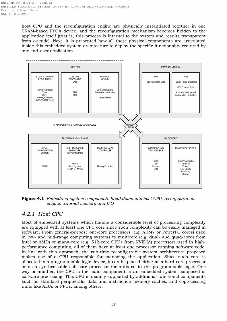
67
host CPU and the reconfiguration engine are physically instantiated together in one SRAM-based FPGA device, and the reconfiguration mechanism becomes hidden to the application itself (that is, this process is internal to the system and results transparent from outside). Next, it is presented how all these physical components are articulated inside this embedded system architecture to deploy the specific functionality required by any end-user application. Figure 4.1 Embedded system components breakdown into host CPU, reconfiguration
engine, external memory and I/O
4.2.1 Host CPU
Most of embedded systems which handle a considerable level of processing complexity are equipped with at least one CPU core since such complexity can be easily managed in software. From general-purpose one-core processors (e.g. ARM7 or PowerPC cores) used in low- and mid-range computing systems to multicore (e.g. dual- and quad-cores from Intel or AMD) or many-core (e.g. 512-core GPUs from NVIDIA) processors used in high-performance computing, all of them have at least one processor running software code. In line with this approach, the run-time reconfigurable system architecture proposed makes use of a CPU responsible for managing the application. Since such core is allocated in a programmable logic device, it can be placed either as a hard-core processor or as a synthesisable soft-core processor instantiated in the programmable logic. One way or another, the CPU is the main component in an embedded system composed of software processing. This CPU is usually supported by additional functional components such as standard peripherals, data and instruction memory caches, and coprocessing units like ALUs or FPUs, among others.
SRAM-BASED PROGRAMMABLE LOGIC DEVICE
RECONFIGURATION ENGINE
HOST CPU
STATIC STANDARD
PERIPHERALS
Interrupt Controller Timer UART
Memory Controller (DDR-SDRAM, Flash)
INTERNAL MEMORY
Data & Instructions (Bootloader, Application)
Cache Memory
CENTRAL
PROCESSING UNIT
FPU ALU
EXTERNAL MEMORY
FPGA
CONFIGURATION MEMORY
SRAM
RUN-TIME RECONF.
HARDWARE COPROCESSORS
Partially Reconfigurable
Region or Partition
RECONFIGURATION
CONTROLLER
Memory Controller
INPUT/OUTPUT
RAM
User-Application Data
NVM
Full and Partial Bitstreams
CPU Program Code
Application Settings and
Configuration Parameters
COMMUNICATION TRANSCEIVERS
RS232 USB
Ethernet CAN
SENSORS/ACTUATORS
Switch/Push Button SmartFET DC Motor
LCD Display LED/Lamp
Camera
CROSSBAR
SWITCH
UNIVERSITAT ROVIRA I VIRGILI EMBEDDED ELECTRONIC SYSTEMS DRIVEN BY RUN-TIME RECONFIGURABLE HARDWARE Francisco Fons Lluís DL: T. 877-2012
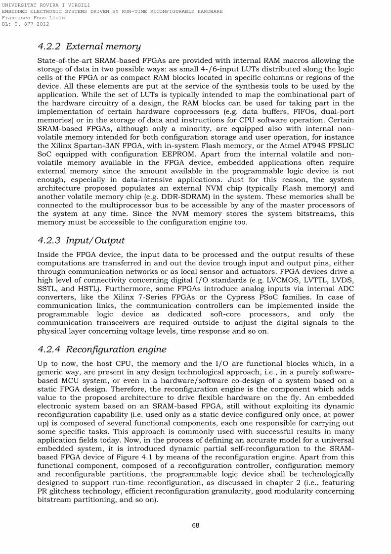
68
4.2.2 External memory
State-of-the-art SRAM-based FPGAs are provided with internal RAM macros allowing the storage of data in two possible ways: as small 4-/6-input LUTs distributed along the logic cells of the FPGA or as compact RAM blocks located in specific columns or regions of the device. All these elements are put at the service of the synthesis tools to be used by the application. While the set of LUTs is typically intended to map the combinational part of the hardware circuitry of a design, the RAM blocks can be used for taking part in the implementation of certain hardware coprocessors (e.g. data buffers, FIFOs, dual-port memories) or in the storage of data and instructions for CPU software operation. Certain SRAM-based FPGAs, although only a minority, are equipped also with internal non-volatile memory intended for both configuration storage and user operation, for instance the Xilinx Spartan-3AN FPGA, with in-system Flash memory, or the Atmel AT94S FPSLIC SoC equipped with configuration EEPROM. Apart from the internal volatile and non-volatile memory available in the FPGA device, embedded applications often require external memory since the amount available in the programmable logic device is not enough, especially in data-intensive applications. Just for this reason, the system architecture proposed populates an external NVM chip (typically Flash memory) and another volatile memory chip (e.g. DDR-SDRAM) in the system. These memories shall be connected to the multiprocessor bus to be accessible by any of the master processors of the system at any time. Since the NVM memory stores the system bitstreams, this memory must be accessible to the configuration engine too.
4.2.3 Input/Output
Inside the FPGA device, the input data to be processed and the output results of these computations are transferred in and out the device trough input and output pins, either through communication networks or as local sensor and actuators. FPGA devices drive a high level of connectivity concerning digital I/O standards (e.g. LVCMOS, LVTTL, LVDS, SSTL, and HSTL). Furthermore, some FPGAs introduce analog inputs via internal ADC converters, like the Xilinx 7-Series FPGAs or the Cypress PSoC families. In case of communication links, the communication controllers can be implemented inside the programmable logic device as dedicated soft-core processors, and only the communication transceivers are required outside to adjust the digital signals to the physical layer concerning voltage levels, time response and so on.
4.2.4 Reconfiguration engine
Up to now, the host CPU, the memory and the I/O are functional blocks which, in a generic way, are present in any design technological approach, i.e., in a purely software-based MCU system, or even in a hardware/software co-design of a system based on a static FPGA design. Therefore, the reconfiguration engine is the component which adds value to the proposed architecture to drive flexible hardware on the fly. An embedded electronic system based on an SRAM-based FPGA, still without exploiting its dynamic reconfiguration capability (i.e. used only as a static device configured only once, at power up) is composed of several functional components, each one responsible for carrying out some specific tasks. This approach is commonly used with successful results in many application fields today. Now, in the process of defining an accurate model for a universal embedded system, it is introduced dynamic partial self-reconfiguration to the SRAM-based FPGA device of Figure 4.1 by means of the reconfiguration engine. Apart from this functional component, composed of a reconfiguration controller, configuration memory and reconfigurable partitions, the programmable logic device shall be technologically designed to support run-time reconfiguration, as discussed in chapter 2 (i.e., featuring PR glitchess technology, efficient reconfiguration granularity, good modularity concerning bitstream partitioning, and so on).
UNIVERSITAT ROVIRA I VIRGILI EMBEDDED ELECTRONIC SYSTEMS DRIVEN BY RUN-TIME RECONFIGURABLE HARDWARE Francisco Fons Lluís DL: T. 877-2012
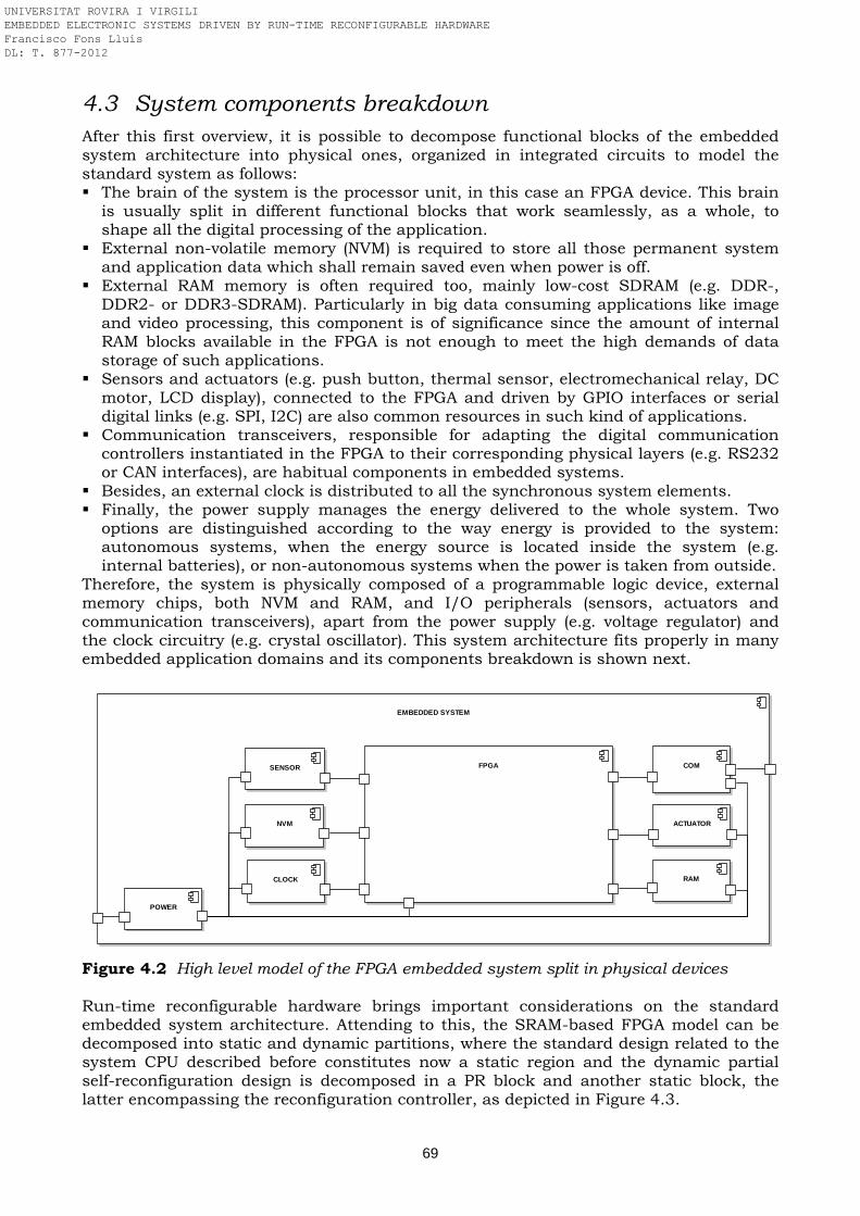
69
4.3 System components breakdown
After this first overview, it is possible to decompose functional blocks of the embedded system architecture into physical ones, organized in integrated circuits to model the standard system as follows: The brain of the system is the processor unit, in this case an FPGA device. This brain
is usually split in different functional blocks that work seamlessly, as a whole, to shape all the digital processing of the application.
External non-volatile memory (NVM) is required to store all those permanent system and application data which shall remain saved even when power is off.
External RAM memory is often required too, mainly low-cost SDRAM (e.g. DDR-, DDR2- or DDR3-SDRAM). Particularly in big data consuming applications like image and video processing, this component is of significance since the amount of internal RAM blocks available in the FPGA is not enough to meet the high demands of data storage of such applications.
Sensors and actuators (e.g. push button, thermal sensor, electromechanical relay, DC motor, LCD display), connected to the FPGA and driven by GPIO interfaces or serial digital links (e.g. SPI, I2C) are also common resources in such kind of applications.
Communication transceivers, responsible for adapting the digital communication controllers instantiated in the FPGA to their corresponding physical layers (e.g. RS232 or CAN interfaces), are habitual components in embedded systems.
Besides, an external clock is distributed to all the synchronous system elements. Finally, the power supply manages the energy delivered to the whole system. Two
options are distinguished according to the way energy is provided to the system: autonomous systems, when the energy source is located inside the system (e.g. internal batteries), or non-autonomous systems when the power is taken from outside.
Therefore, the system is physically composed of a programmable logic device, external memory chips, both NVM and RAM, and I/O peripherals (sensors, actuators and communication transceivers), apart from the power supply (e.g. voltage regulator) and the clock circuitry (e.g. crystal oscillator). This system architecture fits properly in many embedded application domains and its components breakdown is shown next.
EMBEDDED SYSTEM
NVM
RAM
COMSENSOR
ACTUATOR
POWER
CLOCK
FPGA
Figure 4.2 High level model of the FPGA embedded system split in physical devices Run-time reconfigurable hardware brings important considerations on the standard embedded system architecture. Attending to this, the SRAM-based FPGA model can be decomposed into static and dynamic partitions, where the standard design related to the system CPU described before constitutes now a static region and the dynamic partial self-reconfiguration design is decomposed in a PR block and another static block, the latter encompassing the reconfiguration controller, as depicted in Figure 4.3.
UNIVERSITAT ROVIRA I VIRGILI EMBEDDED ELECTRONIC SYSTEMS DRIVEN BY RUN-TIME RECONFIGURABLE HARDWARE Francisco Fons Lluís DL: T. 877-2012
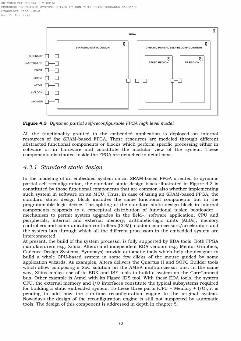
70
FPGA
toSENSOR
toACTUATOR
toNVM
toRAM
toCOM
toCLOCK
toPOWER
STANDARD STATIC DESIGN DYNAMIC PARTIAL SELF-RECONFIGURATION
STATIC REGION PR REGION
Figure 4.3 Dynamic partial self-reconfigurable FPGA high level model All the functionality granted to the embedded application is deployed on internal resources of the SRAM-based FPGA. These resources are modeled through different abstracted functional components or blocks which perform specific processing either in software or in hardware and constitute the modular view of the system. These components distributed inside the FPGA are detached in detail next.
4.3.1 Standard static design In the modeling of an embedded system on an SRAM-based FPGA oriented to dynamic partial self-reconfiguration, the standard static design block illustrated in Figure 4.3 is constituted by those functional components that are common also whether implementing such system in software on an MCU. Thus, in case of using an SRAM-based FPGA, the standard static design block includes the same functional components but in the programmable logic device. The spliting of the standard static design block in internal components responds to a conceptual distribution of functional tasks: bootloader –mechanism to permit system upgrades in the field–, software application, CPU and peripherals, internal and external memory, arithmetic-logic units (ALUs), memory controllers and communication controllers (COM), custom coprocessors/accelerators and the system bus through which all the different processors in the embedded system are interconnected. At present, the build of the system processor is fully supported by EDA tools. Both FPGA manufacturers (e.g. Xilinx, Altera) and independent EDA vendors (e.g. Mentor Graphics, Cadence Design Systems, Synopsys) provide automatic tools which help the designer to build a whole CPU-based system in some few clicks of the mouse guided by some application wizards. As examples, Altera delivers the Quartus II and SOPC Builder tools which allow composing a SoC solution on the AMBA multiprocessor bus. In the same way, Xilinx makes use of its EDK and ISE tools to build a system on the CoreConnect bus. Other example is Atmel with its Figaro IDS tool. With these EDA tools, the system CPU, the external memory and I/O interfaces constitute the typical subsystems required for building a static embedded system. To these three parts (CPU + Memory + I/O), it is pending to add now the run-time reconfiguration engine to the original system. Nowadays the design of the reconfiguration engine is still not supported by automatic tools. The design of this component is addressed in depth in chapter 5.
UNIVERSITAT ROVIRA I VIRGILI EMBEDDED ELECTRONIC SYSTEMS DRIVEN BY RUN-TIME RECONFIGURABLE HARDWARE Francisco Fons Lluís DL: T. 877-2012
71
4.3.2 Dynamic partial self-reconfiguration design
Out of the static standard design block, partial reconfiguration involves additional functional components, some of them deployed as static blocks and others as reconfigurable blocks. The static ones are detailed next: Reconfiguration controller. Any SRAM-based FPGA device is provided with a
configuration mechanism that permits to retrieve a full bitstream from a data repository and download it into the FPGA configuration memory at each power-up. However, in partially reconfigurable FPGA devices, after initial device configuration with a full bitstream, partial bitstreams can be downloaded into the configuration memory of some particular PR regions at run-time. The design of a high bandwidth reconfiguration controller specific for on the fly configurations is required.
PRR interfaces. It is convenient to define a standard interface between the static region and the reconfigurable region. This interface is part of the static design and remains unchanged during the reconfiguration of the PRRs. This standardization lets abstract the application-dependant PR coprocessors from the system architecture and makes possible to build standard coprocessors portable from one platform to another.
These additional static components placed inside the dynamic partial self-reconfiguration block of Figure 4.3 represent the area overhead due to the run-time reconfigurable hardware architecture versus a typical approach based on static hardware and software. This overhead, however, is compensated with the area reserved to partial reconfiguration where different functional PR modules can be multiplexed in time: One or more reconfigurable partitions or PR regions (PRRs) with the convenient area –
i.e., number and type of hardware resources– where specific and custom coprocessors (referred to as partial reconfigurable modules or PRMs) are swapped in and out during the execution of the application. The shape and size of each PRR keeps invariant for all the application life cycle. They constitute the portion of FPGA components to be used as flexible time-shared resources by the application.
Figure 4.3 highlights the fact that the system designer shall minimize the cost in resources of the reconfiguration controller in order to make this run-time reconfigurable approach viable compared to a static implementation. Besides, the continuous reuse of the resources of the PR partitions to fit there different coprocessors each time lets balance the total amount of resources and justify thus the cost savings originated by the use of this technology and architecture in the implementation of embedded applications. Similarly to the balance of area, concerning time, the processing speed up reached by implementing some computational tasks in dedicated hardware (exploiting parallelism) instead of software lets compensate the time overhead originated by the reconfiguration process introduced now in the application execution. Finally, a third term to be balanced with this solution is the power consumption. Therefore, there exists a clear area-time-power trade-off in the design of the standard embedded system architecture proposed.
4.4 System modeling and deployment
This section describes the modeling of a general-purpose electronic system architecture intended for implementing specific embedded applications in reconfigurable hardware and software. The proposed model is oriented to run-time partially reconfigurable SRAM-based FPGA devices – it does not cover single context or multi-context FPGAs according to chapter 2 classification. In a first step, the formal model of the embedded system architecture is particularized to a minimalist approach, being the system composed only of one PR partition and one single data repository. Since the presented architecture is totally scalable, that first approach is extended later in other two more complex scenarios in which the number of PR regions and data repositories increases. Although the model aims to be generic, its physical deployment is conducted on a specific platform, to be exact the commercial Xilinx ML401 evaluation board based on the Xilinx Virtex-4 XC4VLX25 FPGA. The experimental results confirm the feasibility of the model.
UNIVERSITAT ROVIRA I VIRGILI EMBEDDED ELECTRONIC SYSTEMS DRIVEN BY RUN-TIME RECONFIGURABLE HARDWARE Francisco Fons Lluís DL: T. 877-2012
72
4.4.1 Minimalist model: single data repository and single PR partition
The system architecture is based on two computing engines or cores: one host processor which performs tasks in software and one flexible and custom processor which takes charge of the computation of tasks in dedicated hardware. The host processor is placed in a static region of the FPGA and plays the role of a typical CPU to process functionality abstracted in the way of sequential assembler instructions. Similarly, the flexible processor, placed in a PR partition, becomes a dedicated hardware acceleration engine able to self-adapt its computational architecture at run-time to perform any assigned processing task in the most efficient way possible. This flexible computer is frequently seen as a coprocessor attached to the host CPU. The high level of flexibility granted to this system architecture based on a custom reconfigurable hardware computer defined into a partition of the FPGA is possible thanks to the exploitation of SRAM-based programmable logic technology. The powerful computational features of this second processor and its seamless integration into the CPU-based system are undoubtedly the most relevant novelties of the architecture proposed. While the concept of defining a CPU-based system in an FPGA platform is not new, the way of connecting the reconfigurable hardware processor with the host CPU presents certain innovative advances. In this sense, it is observed two types of data accesses to the PR partition, each one pursuing a different purpose: on the one hand, in the reconfiguration process, the partial bitstream is downloaded from the system repository –typically an external memory device– to the internal FPGA configuration memory aimed at changing the features of the processor placed in the PR partition; on the other hand, already in application mode, the processor instantiated in the PR partition must transfer and share some data with the rest of the system. Especially in data-intensive applications, these data are stored in the system repository instead of in internal FPGA memory due to the high volume required. To manage the transfer of both application data and partial bitstreams between the system repository –located in the static region– and the PR partition, the proposed architecture makes use of a master memory management unit (MMU). It is a key component in the system architecture since it lets offload the host CPU from the time-consuming transfers of data required either in the reconfiguration processes or in the processing of tasks inside the PR. Thus, the host processor works in foreground by managing the execution flow of the whole target application and performing some application tasks scheduled in software whereas, in parallel, the master MMU acts as a slave coprocessor that in background supports the reconfiguration and execution of tasks instantiated in the PR partition. From an application point of view, it is convenient that all the processors placed in the PR partition share a common interface to transfer data with the static region of the system. This design constraint is necessary since this interface is implemented in the static region of the FPGA and therefore it can not be modified at run-time. In this sense, the reconfigurable hardware processors instantiated in the PR partition are designed with standard input and output interfaces based on first-in-first-out (FIFO) memories. These FIFO interfaces enable the transfer of data in and out of the PR partition in a standard way –from the system repository to the hardware computer and vice versa– constituting a full-duplex link. Moreover, these FIFOs are implemented with internal RAM blocks of the FPGA, being one port controlled from the static region and the other from the reconfigurable region. The MMU handles the static side of the FIFO whereas the PRMs placed in the PRR takes charge of the FIFO ports accessible from the dynamic side. Other relevant design aspect in the architecture of embedded systems composed of multiple processors is the management of the access to the data repository since it becomes a shared resource. This repository is typically a large external memory device, e.g. a low-cost DDR-SDRAM chip, connected to the pinout of the FPGA. In accordance with the idea of partitioning the end-user application in tasks that are computed concurrently by multiple engines, both CPU and MMU engines need to be master processors to perform writing and reading accesses to the system repository at any time.
UNIVERSITAT ROVIRA I VIRGILI EMBEDDED ELECTRONIC SYSTEMS DRIVEN BY RUN-TIME RECONFIGURABLE HARDWARE Francisco Fons Lluís DL: T. 877-2012
73
For this, the DDR-SDRAM memory is managed by a multi-port memory controller (MPMC implemented in the static region of the FPGA. The multi-port interface allows the different master processors to access the memory from identical or different buses. In our proof-of-concept, the host CPU is connected to the DDR-SDRAM through both CoreConnect PLBv46 and Xilinx CacheLink (XCL) buses while the master MMU is connected via a fast Native Port Interface (NPI) bus. All these buses reach the MPMC and the this controller is who administrates the access of the different sources to the physical DDR-SDRAM at any time, by establishing arbitration mechanisms in case of collisions. Concerning the reconfiguration process, as mentioned above, the master MMU performs the transaction of the configuration bitstream from the system repository to the FPGA configuration memory. In the Virtex-4 FPGA, the datapath to the FPGA configuration memory can be performed through a specific primitive accessible from inside the FPGA logic named internal configuration access port (ICAP). As part of our reconfiguration controller, a finite state machine (FSM) controls the signals of the ICAP interface. This controller is connected with the master MMU through a FIFO memory. Such FIFO plays the role of an intermediate buffer that regulates the data flow, i.e., isolating or making independent the speed in which the data are produced (filled) by the master MMU with respect to the speed in which such data are then consumed (emptied) by the FPGA configuration memory, in accordance with the reconfiguration bandwidth constraints of the particular FPGA in use. Analogously, the FIFOs inserted as standard interfaces between the master MMU and the PR processor let decouple the stage related to the production or consumption of data in the system repository from the counterpart stage in the PR partition. This decoupling feature achieved with FIFOs is a key aspect in this design architecture because just the time independency reached with this approach lets ensure that the custom processors synthesized in the PR partition can be designed without inheriting any technical restriction coming from the rest of the static system (e.g. multiprocessor bus in use, etc). This feature is highly appreciated from the perspective of reusability of IP cores portable to different FPGA platforms. Besides, FIFOs transparently implement blocking-read and blocking-write synchronization mechanisms in case of empty and full buffer scenarios, and the set of control lines which constitute the FIFO wrapper is reasonably small and manageable. Furthermore, hardware modules can read/write from/to FIFOs using a simple, well-known communication protocol instead of other more complex addressing and syncronization schemes. As summary, the use of FIFO memories as standard interfaces among the master MMU, the PR partition and the FPGA configuration memory lets architect a system with multiple clock domains. Besides, a slave MMU is implemented to link the host processor with the master MMU and the PR processor. It consists of a series of configuration registers –some writable and others readable by the host CPU– used as control and status registers for managing the handshake between the master MMU and the PR processor. Through these registers, the CPU can configure a bistream transfer from the repository to the FPGA configuration memory; it is only a matter of specifying to the master MMU the initial address where the bitstream in located in memory and its total size and then give the go-ahead to start the reconfiguration. In parallel, the master MMU notifies the host CPU about the status of this transaction with register flags readable by the host. In addition to the transfer of bitstreams from the system repository to the FPGA configuration memory conducted by the master MMU in each partial reconfiguration, the master MMU is involved in the posterior transfer of data from the repository to that new coprocessor placed in the PR partition. In a similar way, the host CPU configures that transaction by means of configuration registers and the status of this process can be tracked in real-time by specific registers used by the master MMU and accessible at any moment by the host CPU. The same rules apply between the PR processor and the host CPU: specific registers of the slave MMU are written by the host CPU and take effect in the PR processor to initialize some configuration parameters before launching the processing of a specific hardware task. Similarly, the host CPU can be informed about this processing through registers adapted to each custom processor synthesized in the PR partition.
UNIVERSITAT ROVIRA I VIRGILI EMBEDDED ELECTRONIC SYSTEMS DRIVEN BY RUN-TIME RECONFIGURABLE HARDWARE Francisco Fons Lluís DL: T. 877-2012
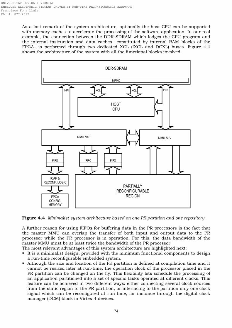
74
DDR-SDRAM
MPMC
NPI XCL XCL
HOST CPU
MMU SLV MMU MST
PARTIALLY RECONFIGURABLE
REGION
ICAP & RECONF. LOGIC
FPGA CONFIG. MEMORY
FIFO FIFO FIFO
PLB
As a last remark of the system architecture, optionally the host CPU can be supported with memory caches to accelerate the processing of the software application. In our real example, the connection between the DDR-SDRAM which lodges the CPU program and the internal instruction and data caches –constituted by internal RAM blocks of the FPGA– is performed through two dedicated XCL (IXCL and DCXL) buses. Figure 4.4 shows the architecture of the system with all the functional blocks involved. Figure 4.4 Minimalist system architecture based on one PR partition and one repository A further reason for using FIFOs for buffering data in the PR processors is the fact that the master MMU can overlap the transfer of both input and output data to the PR processor while the PR processor is in operation. For this, the data bandwidth of the master MMU must be at least twice the bandwidth of the PR processor. The most relevant advantages of this system architecture are highlighted next: It is a minimalist design, provided with the minimum functional components to design
a run-time reconfigurable embedded system. Although the size and location of the PR partition is defined at compilation time and it
cannot be resized later at run-time, the operation clock of the processor placed in the PR partition can be changed on the fly. This flexibility lets schedule the processing of an application partitioned into a set of specific tasks operated at different clocks. This feature can be achieved in two different ways: either connecting several clock sources from the static region to the PR partition, or interfacing to the partition only one clock signal which can be reconfigured at run-time, for instance through the digital clock manager (DCM) block in Virtex-4 devices.
UNIVERSITAT ROVIRA I VIRGILI EMBEDDED ELECTRONIC SYSTEMS DRIVEN BY RUN-TIME RECONFIGURABLE HARDWARE Francisco Fons Lluís DL: T. 877-2012
75
This minimalist approach owns also some drawbacks which, in occasions are accentuated depending on the requirements demanded to the target application: In any programmable logic design, the system designer is always exposed to a time-
area trade-off. That said, the minimalist model is designed with the target of lowest cost in mind. However, in systems based on only one PR partition, the reconfiguration time results in a penalty added to the processing time of the tasks.
An important design aspect linked to this architecture is the effective access to the memory, since this memory is a resource shared between two processors –CPU and master MMU– storing both application data and reconfiguration bitstreams. The master MMU provides data from the repository to two different consumers, the ICAP and the PRR, in addition to sending other data produced by the PRR back to the repository. In this way, the MPMC must dispatch in time all the requests coming from the master MMU and the CPU to not delay the processing. In fact, the bottleneck of many system architectures is found in the fetch and storage of data in memory.
One more limitation in reconfigurable systems composed of only one PR partition is the fixed size of the PRR. Just for this reason, to take the best benefit of this region, all the processors should consume the same number and type of resources. If one PRM placed in the PR partition takes much more resources than the others, this provokes a waste of resources since the size of the biggest PRM delimits the size of the PRR.
Attending to the design constraints of certain applications and aimed at improving the drawbacks discussed above regarding this first approach, other variants of the minimalist model are presented next, focused on reducing the impact of the reconfiguration latency over the application execution time, increasing the bandwidth to access the shared memory and optimizing the PR area reserved to the PR processors by making use of several PR partitions different in size.
4.4.2 Model with single data repository and two PR partitions
In time-critical applications which require fast or frequent switching of PR modules in a PRR, the reconfiguration time can be significant in absolute terms compared to the total execution time of the application. The model proposed in the previous section could reduce or definitively hide its inherent penalty in reconfiguration time by just performing a small change in its architecture. This change consists in adding a second PR partition into the system connected to the same master and slave MMUs. In this way, this redesign presents a reconfigurable system composed of two PR partitions with identical interfaces. The main reason to add the second PR partition is to deploy a bipartitioning strategy of hardware tasks. That is, it is feasible that at any time one PR partition is operative while the other is being reconfigured. Thus, the processing of a given task in one partition is overlapped with the reconfiguration process of the next task in the second partition. For this, the processing time of a hardware task Ti in a PR partition shall take identical or more time than the reconfiguration of the next task Ti+1 conducted in parallel in the other PR partition, and ensuring the fulfilment of this condition for all the hardware tasks which the applitation is split in. To make this model work correctly, the MPMC shall ensure it is able to serve in time all the requests from the host CPU and the master MMU, the latter dealing in this architecture with up to three FIFOs at the same time, one from the reconfiguration process and two from the active PR partition that runs a hardware processor at that moment. In this way, the master MMU supports in parallel the processing of a task and the reconfiguration process of the next one in background. Also of note, the use of two PR partitions offers more flexibility to the system architect to define the size of the PR processors since both partitions can be different in size, shape and types of resources. This fact lets skip more easily the case of having wasted resources in a PRR when a hardware task uses fewer resources than the ones the PRR provides. Furthermore, each PR partition encompasses a different clock domain; therefore, each PR partition can be clocked at a different operation frequency. The new model is illustrated in Figure 4.5.
UNIVERSITAT ROVIRA I VIRGILI EMBEDDED ELECTRONIC SYSTEMS DRIVEN BY RUN-TIME RECONFIGURABLE HARDWARE Francisco Fons Lluís DL: T. 877-2012
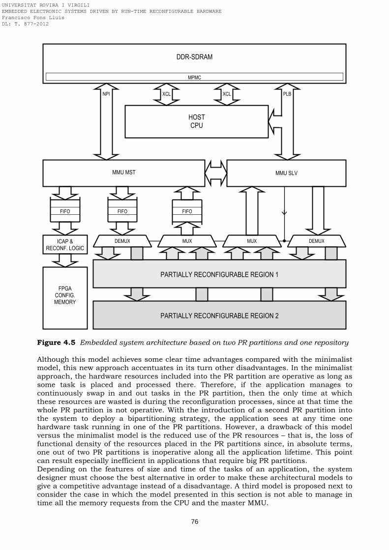
76
Figure 4.5 Embedded system architecture based on two PR partitions and one repository Although this model achieves some clear time advantages compared with the minimalist model, this new approach accentuates in its turn other disadvantages. In the minimalist approach, the hardware resources included into the PR partition are operative as long as some task is placed and processed there. Therefore, if the application manages to continuously swap in and out tasks in the PR partition, then the only time at which these resources are wasted is during the reconfiguration processes, since at that time the whole PR partition is not operative. With the introduction of a second PR partition into the system to deploy a bipartitioning strategy, the application sees at any time one hardware task running in one of the PR partitions. However, a drawback of this model versus the minimalist model is the reduced use of the PR resources – that is, the loss of functional density of the resources placed in the PR partitions since, in absolute terms, one out of two PR partitions is inoperative along all the application lifetime. This point can result especially inefficient in applications that require big PR partitions. Depending on the features of size and time of the tasks of an application, the system designer must choose the best alternative in order to make these architectural models to give a competitive advantage instead of a disadvantage. A third model is proposed next to consider the case in which the model presented in this section is not able to manage in time all the memory requests from the CPU and the master MMU.
DDR-SDRAM
MPMC
NPI XCL XCL
HOST CPU
MMU SLV MMU MST
PARTIALLY RECONFIGURABLE REGION 2
ICAP & RECONF. LOGIC
FPGA CONFIG. MEMORY
FIFO FIFO FIFO
DEMUX MUX DEMUX MUX
PARTIALLY RECONFIGURABLE REGION 1
PLB
UNIVERSITAT ROVIRA I VIRGILI EMBEDDED ELECTRONIC SYSTEMS DRIVEN BY RUN-TIME RECONFIGURABLE HARDWARE Francisco Fons Lluís DL: T. 877-2012
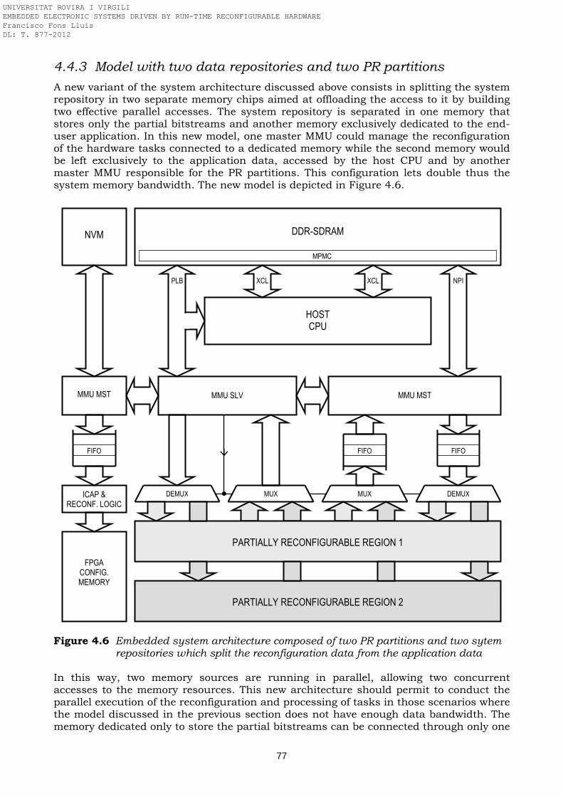
77
4.4.3 Model with two data repositories and two PR partitions
A new variant of the system architecture discussed above consists in splitting the system repository in two separate memory chips aimed at offloading the access to it by building two effective parallel accesses. The system repository is separated in one memory that stores only the partial bitstreams and another memory exclusively dedicated to the end-user application. In this new model, one master MMU could manage the reconfiguration of the hardware tasks connected to a dedicated memory while the second memory would be left exclusively to the application data, accessed by the host CPU and by another master MMU responsible for the PR partitions. This configuration lets double thus the system memory bandwidth. The new model is depicted in Figure 4.6.
Figure 4.6 Embedded system architecture composed of two PR partitions and two sytem
repositories which split the reconfiguration data from the application data In this way, two memory sources are running in parallel, allowing two concurrent accesses to the memory resources. This new architecture should permit to conduct the parallel execution of the reconfiguration and processing of tasks in those scenarios where the model discussed in the previous section does not have enough data bandwidth. The memory dedicated only to store the partial bitstreams can be connected through only one
NVM
XCL
HOST CPU
MMU MST MMU MST
PARTIALLY RECONFIGURABLE REGION 2
ICAP & RECONF. LOGIC
FPGA CONFIG. MEMORY
XCL
FIFO FIFO FIFO
DEMUX MUX DEMUX MUX
PARTIALLY RECONFIGURABLE REGION 1
MMU SLV
NPI
DDR-SDRAM
MPMC
PLB
UNIVERSITAT ROVIRA I VIRGILI EMBEDDED ELECTRONIC SYSTEMS DRIVEN BY RUN-TIME RECONFIGURABLE HARDWARE Francisco Fons Lluís DL: T. 877-2012
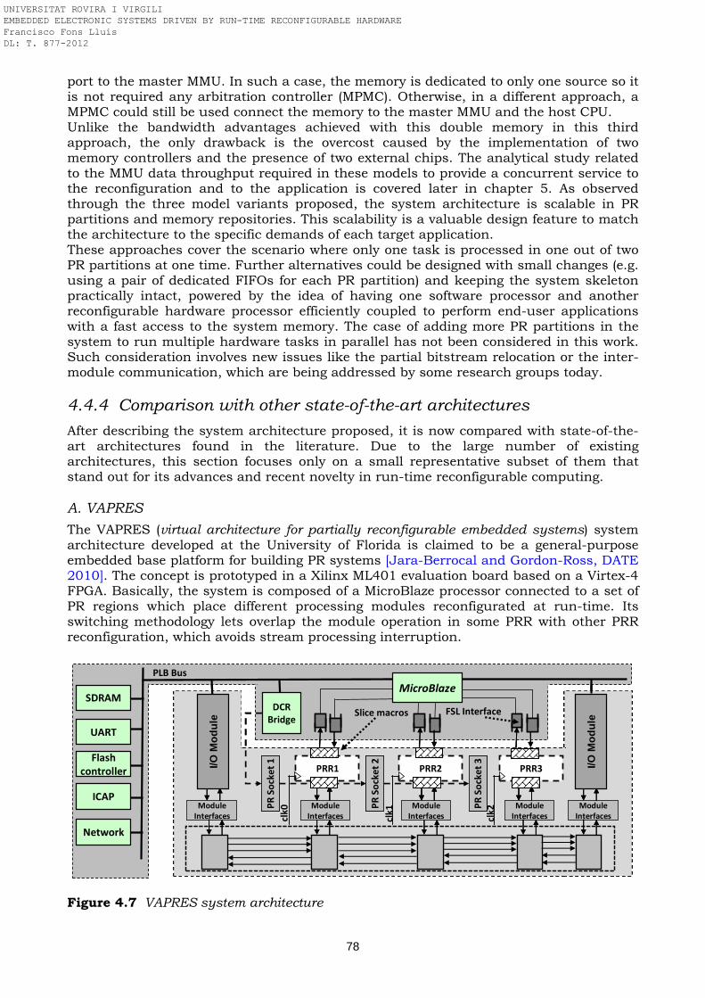
78
port to the master MMU. In such a case, the memory is dedicated to only one source so it is not required any arbitration controller (MPMC). Otherwise, in a different approach, a MPMC could still be used connect the memory to the master MMU and the host CPU. Unlike the bandwidth advantages achieved with this double memory in this third approach, the only drawback is the overcost caused by the implementation of two memory controllers and the presence of two external chips. The analytical study related to the MMU data throughput required in these models to provide a concurrent service to the reconfiguration and to the application is covered later in chapter 5. As observed through the three model variants proposed, the system architecture is scalable in PR partitions and memory repositories. This scalability is a valuable design feature to match the architecture to the specific demands of each target application. These approaches cover the scenario where only one task is processed in one out of two PR partitions at one time. Further alternatives could be designed with small changes (e.g. using a pair of dedicated FIFOs for each PR partition) and keeping the system skeleton practically intact, powered by the idea of having one software processor and another reconfigurable hardware processor efficiently coupled to perform end-user applications with a fast access to the system memory. The case of adding more PR partitions in the system to run multiple hardware tasks in parallel has not been considered in this work. Such consideration involves new issues like the partial bitstream relocation or the inter-module communication, which are being addressed by some research groups today.
4.4.4 Comparison with other state-of-the-art architectures
After describing the system architecture proposed, it is now compared with state-of-the-art architectures found in the literature. Due to the large number of existing architectures, this section focuses only on a small representative subset of them that stand out for its advances and recent novelty in run-time reconfigurable computing. A. VAPRES
The VAPRES (virtual architecture for partially reconfigurable embedded systems) system architecture developed at the University of Florida is claimed to be a general-purpose embedded base platform for building PR systems [Jara-Berrocal and Gordon-Ross, DATE 2010]. The concept is prototyped in a Xilinx ML401 evaluation board based on a Virtex-4 FPGA. Basically, the system is composed of a MicroBlaze processor connected to a set of PR regions which place different processing modules reconfigurated at run-time. Its switching methodology lets overlap the module operation in some PRR with other PRR reconfiguration, which avoids stream processing interruption.
Figure 4.7 VAPRES system architecture
PRR1 PRR2 PRR3
FSL Interface
PLB Bus
Module
Interfaces
Module
Interfaces
Module
Interfacesclk
1
clk
2
clk
0
ICAP
Flash
controller
UART
SDRAM
Network
I/O M
od
ule
I/O M
od
ule
DCR
Bridge
Module
Interfaces
Module
Interfaces
MicroBlaze
PR
So
cke
t 1
PR
So
cke
t 2
PR
So
cke
t 3
Slice macros
PRR1 PRR2 PRR3
FSL Interface
PLB Bus
Module
Interfaces
Module
Interfaces
Module
Interfacesclk
1
clk
2
clk
0
ICAP
Flash
controller
UART
SDRAM
Network
I/O M
od
ule
I/O M
od
ule
DCR
Bridge
Module
Interfaces
Module
Interfaces
MicroBlaze
PR
So
cke
t 1
PR
So
cke
t 2
PR
So
cke
t 3
PR
So
cke
t 1
PR
So
cke
t 2
PR
So
cke
t 3
Slice macros
UNIVERSITAT ROVIRA I VIRGILI EMBEDDED ELECTRONIC SYSTEMS DRIVEN BY RUN-TIME RECONFIGURABLE HARDWARE Francisco Fons Lluís DL: T. 877-2012
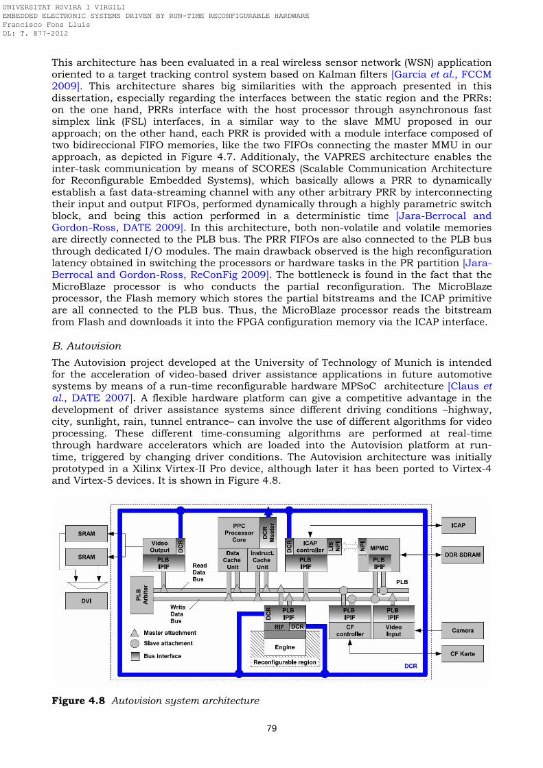
79
This architecture has been evaluated in a real wireless sensor network (WSN) application oriented to a target tracking control system based on Kalman filters [Garcia et al., FCCM 2009]. This architecture shares big similarities with the approach presented in this dissertation, especially regarding the interfaces between the static region and the PRRs: on the one hand, PRRs interface with the host processor through asynchronous fast simplex link (FSL) interfaces, in a similar way to the slave MMU proposed in our approach; on the other hand, each PRR is provided with a module interface composed of two bidireccional FIFO memories, like the two FIFOs connecting the master MMU in our approach, as depicted in Figure 4.7. Additionaly, the VAPRES architecture enables the inter-task communication by means of SCORES (Scalable Communication Architecture for Reconfigurable Embedded Systems), which basically allows a PRR to dynamically establish a fast data-streaming channel with any other arbitrary PRR by interconnecting their input and output FIFOs, performed dynamically through a highly parametric switch block, and being this action performed in a deterministic time [Jara-Berrocal and Gordon-Ross, DATE 2009]. In this architecture, both non-volatile and volatile memories are directly connected to the PLB bus. The PRR FIFOs are also connected to the PLB bus through dedicated I/O modules. The main drawback observed is the high reconfiguration latency obtained in switching the processors or hardware tasks in the PR partition [Jara-Berrocal and Gordon-Ross, ReConFig 2009]. The bottleneck is found in the fact that the MicroBlaze processor is who conducts the partial reconfiguration. The MicroBlaze processor, the Flash memory which stores the partial bitstreams and the ICAP primitive are all connected to the PLB bus. Thus, the MicroBlaze processor reads the bitstream from Flash and downloads it into the FPGA configuration memory via the ICAP interface. B. Autovision
The Autovision project developed at the University of Technology of Munich is intended for the acceleration of video-based driver assistance applications in future automotive systems by means of a run-time reconfigurable hardware MPSoC architecture [Claus et al., DATE 2007]. A flexible hardware platform can give a competitive advantage in the development of driver assistance systems since different driving conditions –highway, city, sunlight, rain, tunnel entrance– can involve the use of different algorithms for video processing. These different time-consuming algorithms are performed at real-time through hardware accelerators which are loaded into the Autovision platform at run-time, triggered by changing driver conditions. The Autovision architecture was initially prototyped in a Xilinx Virtex-II Pro device, although later it has been ported to Virtex-4 and Virtex-5 devices. It is shown in Figure 4.8.
Figure 4.8 Autovision system architecture
UNIVERSITAT ROVIRA I VIRGILI EMBEDDED ELECTRONIC SYSTEMS DRIVEN BY RUN-TIME RECONFIGURABLE HARDWARE Francisco Fons Lluís DL: T. 877-2012
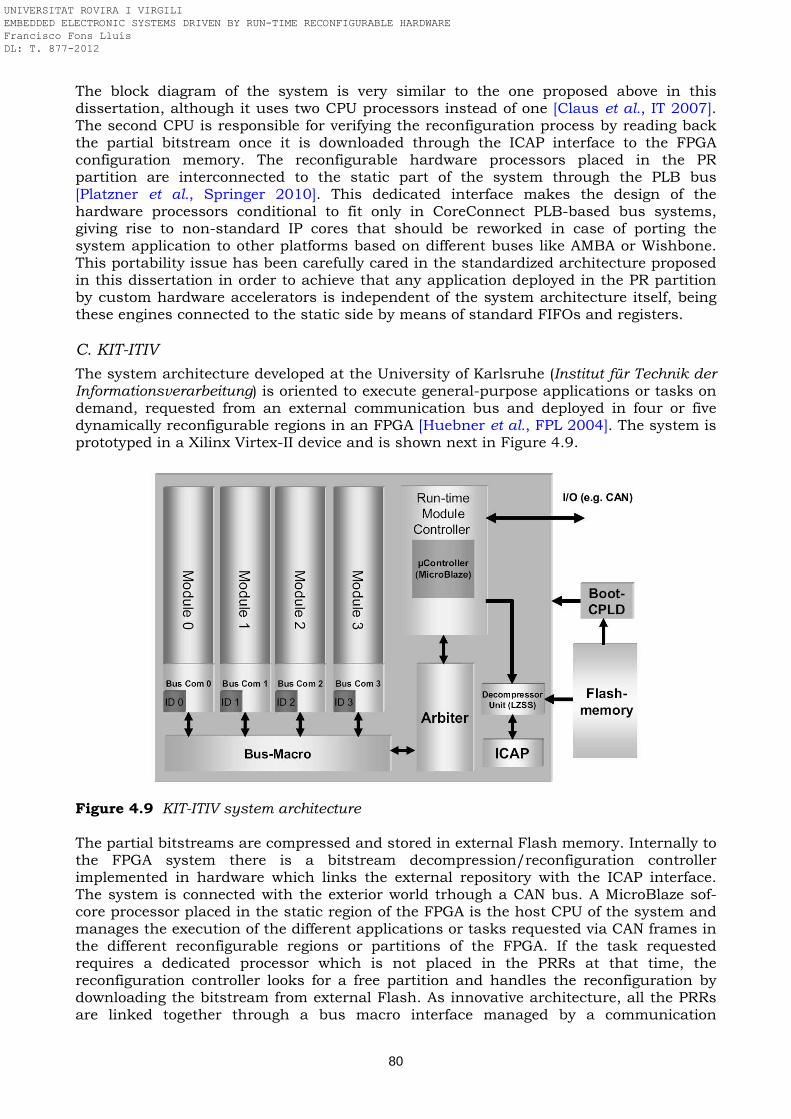
80
The block diagram of the system is very similar to the one proposed above in this dissertation, although it uses two CPU processors instead of one [Claus et al., IT 2007]. The second CPU is responsible for verifying the reconfiguration process by reading back the partial bitstream once it is downloaded through the ICAP interface to the FPGA configuration memory. The reconfigurable hardware processors placed in the PR partition are interconnected to the static part of the system through the PLB bus [Platzner et al., Springer 2010]. This dedicated interface makes the design of the hardware processors conditional to fit only in CoreConnect PLB-based bus systems, giving rise to non-standard IP cores that should be reworked in case of porting the system application to other platforms based on different buses like AMBA or Wishbone. This portability issue has been carefully cared in the standardized architecture proposed in this dissertation in order to achieve that any application deployed in the PR partition by custom hardware accelerators is independent of the system architecture itself, being these engines connected to the static side by means of standard FIFOs and registers. C. KIT-ITIV
The system architecture developed at the University of Karlsruhe (Institut für Technik der Informationsverarbeitung) is oriented to execute general-purpose applications or tasks on demand, requested from an external communication bus and deployed in four or five dynamically reconfigurable regions in an FPGA [Huebner et al., FPL 2004]. The system is prototyped in a Xilinx Virtex-II device and is shown next in Figure 4.9.
Figure 4.9 KIT-ITIV system architecture The partial bitstreams are compressed and stored in external Flash memory. Internally to the FPGA system there is a bitstream decompression/reconfiguration controller implemented in hardware which links the external repository with the ICAP interface. The system is connected with the exterior world trhough a CAN bus. A MicroBlaze sof-core processor placed in the static region of the FPGA is the host CPU of the system and manages the execution of the different applications or tasks requested via CAN frames in the different reconfigurable regions or partitions of the FPGA. If the task requested requires a dedicated processor which is not placed in the PRRs at that time, the reconfiguration controller looks for a free partition and handles the reconfiguration by downloading the bitstream from external Flash. As innovative architecture, all the PRRs are linked together through a bus macro interface managed by a communication
UNIVERSITAT ROVIRA I VIRGILI EMBEDDED ELECTRONIC SYSTEMS DRIVEN BY RUN-TIME RECONFIGURABLE HARDWARE Francisco Fons Lluís DL: T. 877-2012
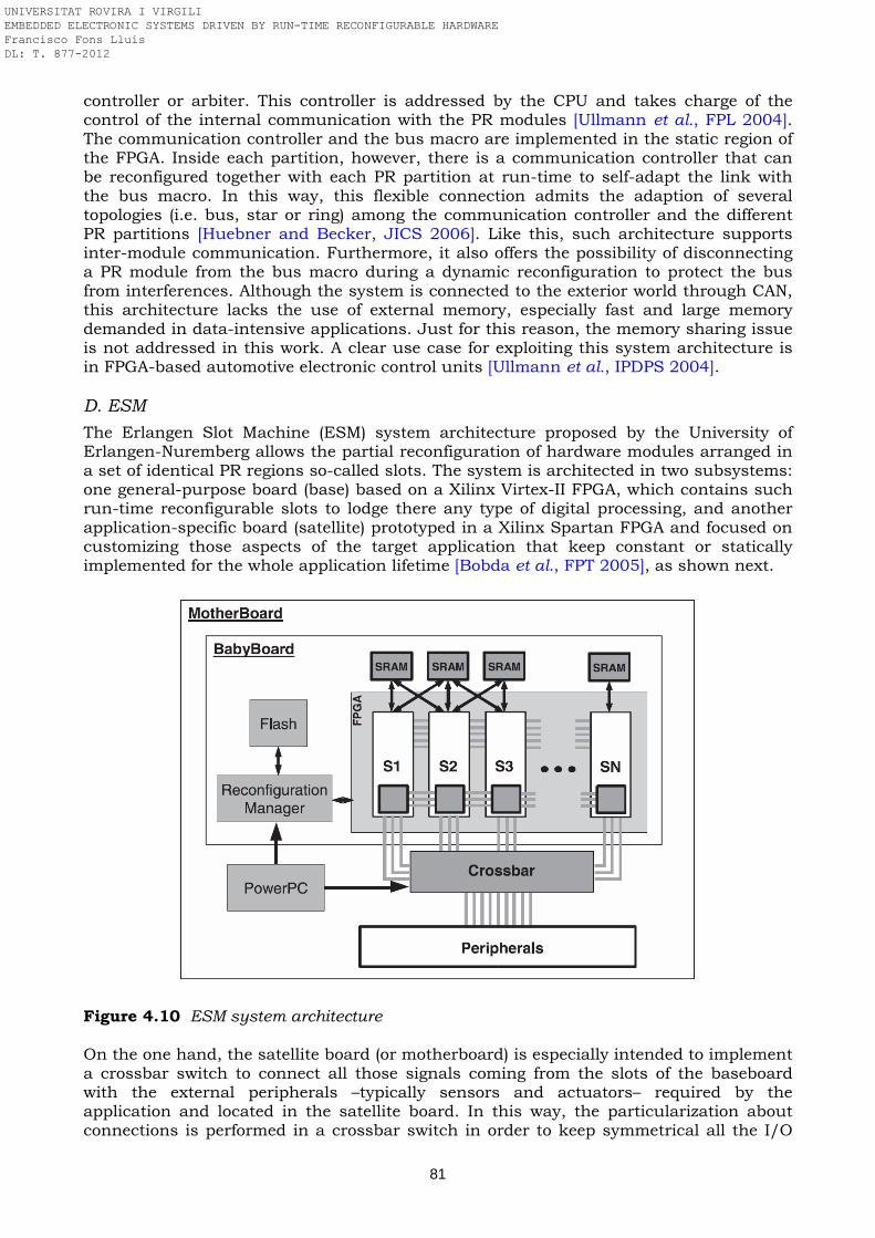
81
controller or arbiter. This controller is addressed by the CPU and takes charge of the control of the internal communication with the PR modules [Ullmann et al., FPL 2004]. The communication controller and the bus macro are implemented in the static region of the FPGA. Inside each partition, however, there is a communication controller that can be reconfigured together with each PR partition at run-time to self-adapt the link with the bus macro. In this way, this flexible connection admits the adaption of several topologies (i.e. bus, star or ring) among the communication controller and the different PR partitions [Huebner and Becker, JICS 2006]. Like this, such architecture supports inter-module communication. Furthermore, it also offers the possibility of disconnecting a PR module from the bus macro during a dynamic reconfiguration to protect the bus from interferences. Although the system is connected to the exterior world through CAN, this architecture lacks the use of external memory, especially fast and large memory demanded in data-intensive applications. Just for this reason, the memory sharing issue is not addressed in this work. A clear use case for exploiting this system architecture is in FPGA-based automotive electronic control units [Ullmann et al., IPDPS 2004]. D. ESM
The Erlangen Slot Machine (ESM) system architecture proposed by the University of Erlangen-Nuremberg allows the partial reconfiguration of hardware modules arranged in a set of identical PR regions so-called slots. The system is architected in two subsystems: one general-purpose board (base) based on a Xilinx Virtex-II FPGA, which contains such run-time reconfigurable slots to lodge there any type of digital processing, and another application-specific board (satellite) prototyped in a Xilinx Spartan FPGA and focused on customizing those aspects of the target application that keep constant or statically implemented for the whole application lifetime [Bobda et al., FPT 2005], as shown next.
Figure 4.10 ESM system architecture On the one hand, the satellite board (or motherboard) is especially intended to implement a crossbar switch to connect all those signals coming from the slots of the baseboard with the external peripherals –typically sensors and actuators– required by the application and located in the satellite board. In this way, the particularization about connections is performed in a crossbar switch in order to keep symmetrical all the I/O
UNIVERSITAT ROVIRA I VIRGILI EMBEDDED ELECTRONIC SYSTEMS DRIVEN BY RUN-TIME RECONFIGURABLE HARDWARE Francisco Fons Lluís DL: T. 877-2012
82
pinout connections of the slots in the baseboard. This aspect helps to promote the bistream relocation by reducing the complexity in the baseboard whereas the crossbar switch takes charge of establishing the connections in the satellite board which is application-specific. Apart from the crossbar switch, the satellite board also contains a PowerPC processor for managing the data flow and the communication with the exterior world. On the other hand, the baseboard (also called baby board) contains six identical slots inside the Virtex-II FPGA. Each slot is connected to a dedicated external SRAM memory to support the data processing carried out in that slot or its neighbours in left and right sides. This architecture gives solution to the inter-module communication through several options: bus macros, shared memory, reconfigurable multiple buses or external crossbar switch [Majer et al., VLSI 2007]. A reconfiguration manager is in charge of placing the partial bitstream indistinctly in any of the slots possible. As proof-of-concept, this platform has been used in modular video streaming applications. The main advantage of the ESM platform is the flexibility in communication, uniformity of resource distribution and placement freedom by means of relocation. The main disadvantage is the big number of components (BOM), which makes this approach prohibitive in some cost-sensitive applications. However, although some restrictions come from the non-support for two-dimensional reconfigurability of the Virtex-II FPGA (full-column reconfiguration only), these ideas can be ported to a 2D-reconfigurable FPGA (e.g. Virtex-4) and implement the crossbar switch in the static region of the device. E. Molen
Developed at the Delft University of Technology, the Molen architecture addresses both general-purpose and custom computing in one hybrid field-programmable custom computing machine [Vassiliadis et al., TC 2004]. It copes with a reconfigurable coprocessing extension seamlessly coupled to a processor, all prototyped in a Xilinx Virtex-II Pro FPGA. The PowerPC hard core embedded in the FPGA is operating as a general-purpose processor while the reconfigurable fabric is used as a reconfigurable coprocessor [Kuzmanov et al., SAMOS 2004]. Additionally, some exchange registers (XREG) are introduced to communicate the reconfigurable processor with the core processor giving rise to an architectural coupling. Moreover, this coupling is performed at the level of an assembler instructions extension: some few instructions are added to the original assembler instructions set of the core processor to drive the coprocessor. The minimal extension comprises only four instructions: two instructions (set/execute) for loading a hardware implementation and launching its execution on the reconfigurable hardware, and two instructions (movtx/movfx) for providing the communication via XREG registers between the reconfigurable hardware and the general-purpose processor. The two main components in the Molen machine organization are the Core Processor, which is a general-purpose processor, and the Reconfigurable Processor. The main memory stores the program code, the application data and the partial bitstreams. Instructions are fetched from the main memory and issued to either processor by the Arbiter. Data are fetched/stored by the Data Fetch unit. The Memory Mux/Demux unit is responsible for distributing/collecting data. The reconfigurable processor is divided in two units: the Reconfigurable Microcode (ρµ-code) Unit and the Custom Configuration Unit (CCU). The CCU consists of reconfigurable hardware (e.g. FPGA) and memory. The ρµ-code unit is responsible for controlling the downloading of the partial bitstream from the main memory to the FPGA configuration memory. This role assigned to the ρµ-code unit is deployed when executing the instructions set/execute during the reconfiguration and the next execution of the reconfigurable task: the set phase can be scheduled well ahead of the execute phase, thereby hiding the reconfiguration latency. After the reconfiguration, the role of the ρµ-code unit is to communicate the CCU with the core processor, taking care of the exchange of function parameters and results between both processors through the movtx/movfx instructions [Kuzmanov et al., SAMOS 2003]. The system architecture detached in functional blocks is depicted next.
UNIVERSITAT ROVIRA I VIRGILI EMBEDDED ELECTRONIC SYSTEMS DRIVEN BY RUN-TIME RECONFIGURABLE HARDWARE Francisco Fons Lluís DL: T. 877-2012
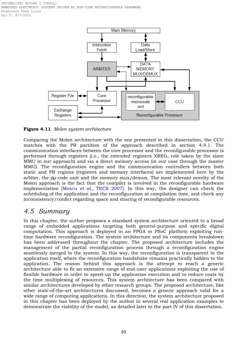
83
Figure 4.11 Molen system architecture Comparing the Molen architecture with the one presented in this dissertation, the CCU matches with the PR partition of the approach described in section 4.4.1. The communication interfaces between the core processor and the reconfigurable processor is performed through registers (i.e., the extended registers XREG, role taken by the slave MMU in our approach) and via a direct memory access (in our case through the master MMU). The reconfiguration engine and the communication controllers between both static and PR regions (registers and memory interfaces) are implemented here by the arbiter, the ρµ-code unit and the memory mux/demux. The most relevant novelty of the Molen approach is the fact that the compiler is involved in the reconfigurable hardware implementation [Moscu et al., TECS 2007]. In this way, the designer can check the scheduling of the application and the reconfiguration at compilation time, and check any inconsistency/confict regarding space and sharing of reconfigurable resources.
4.5 Summary
In this chapter, the author proposes a standard system architecture oriented to a broad range of embedded applications targeting both general-purpose and specific digital computation. This approach is deployed in an FPGA or PSoC platform exploiting run-time hardware reconfiguration. The system architecture and its components breakdown has been addressed throughout the chapter. The proposed architecture includes the management of the partial reconfiguration process through a reconfiguration engine seamlessly merged to the system. In this way, the reconfiguration is transparent to the application itself, where the reconfiguration handshake remains practically hidden to the application. The reason behind this approach is the attempt to reach a generic architecture able to fit an extensive range of end-user applications exploiting the use of flexible hardware in order to speed-up the application execution and to reduce costs by the time multiplexing of resources. This system architecture has been compared with similar architectures developed by other research groups. The proposed architecture, like other state-of-the-art architectures discussed, becomes a generic approach valid for a wide range of computing applications. In this direction, the system architecture proposed in this chapter has been deployed by the author in several real application examples to demonstrate the viability of the model, as detailed later in the part IV of this dissertation.
UNIVERSITAT ROVIRA I VIRGILI EMBEDDED ELECTRONIC SYSTEMS DRIVEN BY RUN-TIME RECONFIGURABLE HARDWARE Francisco Fons Lluís DL: T. 877-2012
84
References
[Bobda et al., FPT 2005] C. Bobda, A. Majer, A. Ahmadinia, T. Haller, A. Linarth, J. Teich, The Erlangen Slot Machine: Increasing flexibility in FPGA-based reconfigurable platforms, Proceedings of the IEEE International Conference on Field-Programmable Technology, pp. 37-42, 2005.
[Claus et al., DATE 2007] C. Claus, J. Zeppenfeld, F. Müller, W. Stechele, Using partial-run-time reconfigurable hardware to accelerate video processing in driver assistance systems, Proceedings of the Conference and Exhibition on Design, Automation, and Test in Europe, pp. 498–503, 2007.
[Claus et al., IT 2007] C. Claus, W. Stechele, A. Herkersdorf, Autovision – A run-time reconfigurable MPSoC architecture for future driver assistance systems, Information Technology, vol. 49, no. 3, pp. 181-187, 2007.
[Garcia et al., FCCM 2009] R. Garcia, A. Gordon-Ross, A. George, Exploiting partially reconfigurable FPGAs for situation-based reconfiguration in wireless sensor networks, Proceedings of the IEEE Symposium on Field Programmable Custom Computing Machines, pp.243-246, 2009.
[Huebner and Becker, JICS 2006] M. Huebner, J. Becker, Dynamic and partial FPGA self-reconfiguration using real-time LUT-based network-on-chip adaptive topologies for Xilinx FPGAs, Journal Integrated Circuits and Systems, vol. 1, no. 4, pp. 43-53, 2006.
[Huebner et al., FPL 2004] M. Huebner, M. Ullmann, L. Braun, A. Klausmann, J. Becker, Scalable application-dependent network on chip adaptivity for dynamical reconfigurable real-time systems, Proc. Int. Conf. on Field Programmable Logic and Applications, LNCS, vol. 3203, pp. 1037-1041, Springer-Verlag, 2004.
[Jara-Berrocal and Gordon-Ross, DATE 2009] A. Jara-Berrocal, A. Gordon-Ross, SCORES: A scalable and parametric streams-based communication architecture for modular reconfigurable systems, Proceedings of the Conference and Exhibition on Design, Automation, and Test in Europe, pp. 268-273, 2009.
[Jara-Berrocal and Gordon-Ross, DATE 2010] A. Jara-Berrocal, A. Gordon-Ross, VAPRES: A virtual architecture for partially reconfigurable embedded systems, Proc. Conf. and Exhibition on Design, Automation, and Test in Europe, pp. 837-842, 2010.
[Jara-Berrocal and Gordon-Ross, ReConFig 2009] A. Jara-Berrocal, A. Gordon-Ross, Runtime temporal partitioning assembly to reduce FPGA reconfiguration time, Proc. Int. Conf. on Reconfigurable Computing and FPGAs, pp. 374-379, 2009.
[Kuzmanov et al., SAMOS 2003] G. Kuzmanov, G.N. Gaydadjiev, S. Vassiliadis, Loading rm-code: Design considerations, Proceedings of the International Workshop on Computer Systems: Architectures, Modeling, and Simulation (SAMOS), LNCS, vol. 3133, pp. 11-19, Springer-Verlag, 2003.
[Kuzmanov et al., SAMOS 2004] G.K. Kuzmanov, G.N. Gaydadjiev, S. Vassiliadis, The Virtex II Pro™ MOLEN processor, Proceedings of the International Workshop on Computer Systems: Architectures, Modelling, and Simulation, LNCS, vol. 3133, pp. 192-202, Springer-Verlag, 2004.
[Majer et al., VLSI 2007] M. Majer, J. Teich, A. Ahmadinia, C. Bobda, The Erlangen Slot Machine: A dynamically reconfigurable FPGA-based computer, The Journal of VLSI Signal Processing, vol. 47, no. 1, pp. 15-31, 2007.
[Moscu et al., TECS 2007] E. Moscu Panainte, K. Bertels, S. Vassiliadis, The Molen compiler for reconfigurable processors, ACM Transactions in Embedded Computing Systems, vol. 6, no. 1, pp. 1-18, 2007.
[Platzner et al., Springer 2010] M. Platzner, J. Teich, N. Wehn (Eds.), Dynamically reconfigurable systems - Architectures, design methods and applications, Springer, ISBN 978-90-481-3484-7, 2010.
[Ullmann et al., FPL 2004] M. Ullmann, M. Hübner, B. Grimm, J. Becker, On-demand FPGA run-time system for dynamical reconfiguration with adaptive priorities, Proc. of the Int.Conference on Field Programmable Logic and Applications, LNCS, vol. 3203, pp. 454-463, Springer-Verlag, 2004.
[Ullmann et al., IPDPS 2004] M. Ullmann, M. Hübner, B. Grimm, J. Becker, An FPGA run-time system for dynamic on-demand reconfiguration, Proceedings of the International Parallel and Distributed Processing Symposium, 2004.
[Vassiliadis et al., TC 2004] S. Vassiliadis, G. Gaydadjiev, G. Kuzmanov, The MOLEN polymorphic processor, IEEE Transactions on Computers, vol. 53, no. 11, pp. 1363-1375, 2004.
UNIVERSITAT ROVIRA I VIRGILI EMBEDDED ELECTRONIC SYSTEMS DRIVEN BY RUN-TIME RECONFIGURABLE HARDWARE Francisco Fons Lluís DL: T. 877-2012
85
Chapter 5 Reconfiguration engine This chapter focuses on the mechanism which allows an SRAM-based programmable logic device to partially or fully reconfigure its logic resources at run-time, while the rest of its non-reconfigured/non-reconfigurable resources continue in operation without suffering any interruption (i.e., operation discontinuity) or affectation (i.e., malfunction), and making the reconfigured blocks –just after concluding the reconfiguration– restart their activity to join thus the rest of device already in operation. As part of the functional components which constitute the embedded reconfigurable system architecture promoted in the previous chapter, next it is presented the design features of the reconfiguration engine as well as the technological characteristics demanded to the SRAM-based programmable logic device that shall harbour it. After evaluating different closed (e.g. Atmel, Altera) and open (e.g. Xilinx) reconfiguration engine solutions applied to embedded systems based on FPGA or PSoC devices, the author details step by step the modeling of the reconfiguration engine proposed.
5.1 Reconfiguration design parameters
As introduced in chapter 4, given an embedded system based on an SRAM-based programmable logic device provided with run-time reconfigurable hardware technology, the reconfiguration engine is is one of the basic components in the system architecture. Apart from the bitstreams repository, typically composed of an external non-volatile or volatile memory chip, the reconfiguration engine is constituted by three functional blocks which build the reconfiguration datapath, as illustrated in Figure 4.1: the SRAM-based configuration memory of the programmable logic device, the PR partitions which delimit the set of resources subject to be reconfigured at run-time, and the reconfiguration controller which manages the transfer of the partial bitstreams from the repository to the internal configuration memory. Attending to features of the reconfiguration controller, certain programmable logic devices allow conducting the dynamic reconfiguration of their resources by themselves, that is, in an autonomous way – without requiring the help of any external logic. For this, these devices include in their fabric the complete reconfiguration logic. Other approaches are based on the use of external devices to implement the logic that controls the reconfiguration, for instance through an external processor or MCU responsible for carrying out the bistream transfer, or by means of an external CPLD which implements the specific controller, or even embedding this controller in the repository memory chip (e.g. platform flash PROM devices, composed of flash memory and a controller provided with an integrated bitstream delivery mechanism adapted to the transfer protocol of the Xilinx FPGA devices). Figure 5.1 shows these two different reconfiguration approaches: self-reconfiguration and external reconfiguration, in function of whether the reconfiguration controller is placed inside the FPGA or outside. In the block diagram, the reconfiguration controller is shown split in two parts, making a clear distinction between the functional block that takes care of translating the FPGA raw data received through the bitstream frames to be loaded into the internal FPGA configuration memory –called reconfiguration logic– and the logic block responsible for handling the high-level control and handshake of the bitstream transfer between the external memory and the FPGA – called reconfiguration controller. Both logic blocks are connected via the reconfiguration port. The reconfiguration efficiency is function of a large number of design parameters that shall be carefully evaluated, as discussed in chapter 2. Design parameters related to the technology of the programmable logic device –like reconfiguration granularity, bitstream
UNIVERSITAT ROVIRA I VIRGILI EMBEDDED ELECTRONIC SYSTEMS DRIVEN BY RUN-TIME RECONFIGURABLE HARDWARE Francisco Fons Lluís DL: T. 877-2012
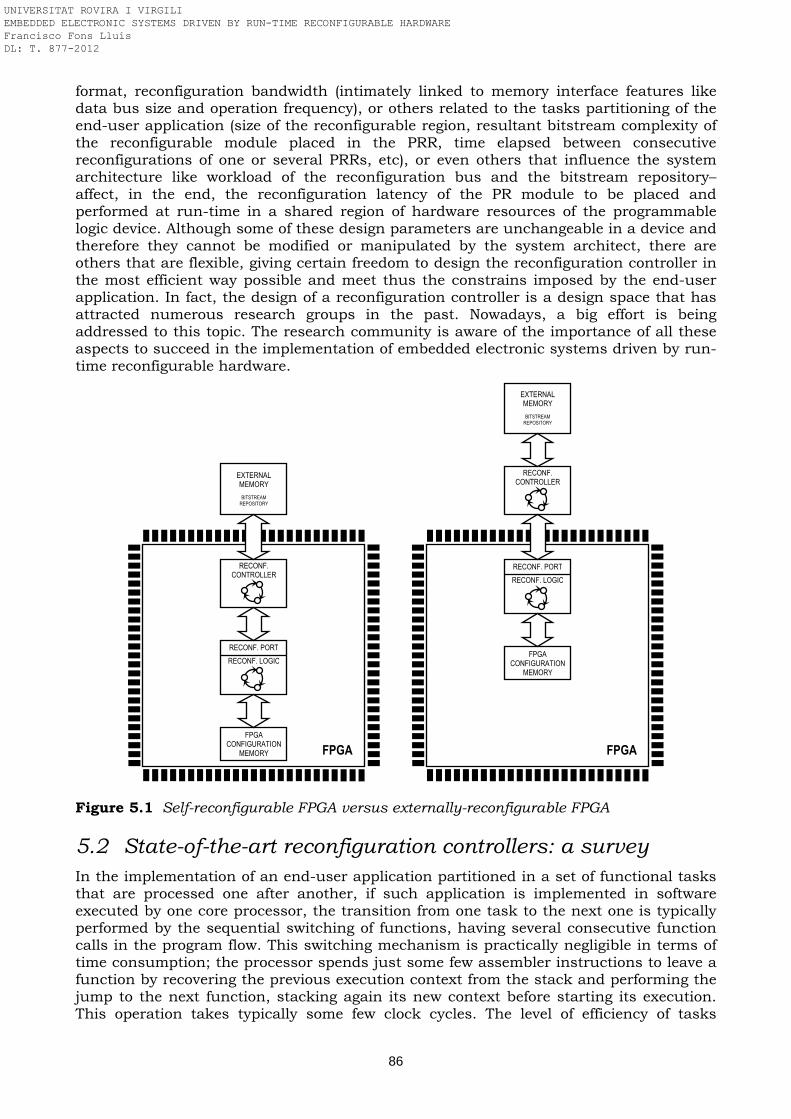
86
RECONF. CONTROLLER
RECONF. PORT
FPGA CONFIGURATION
MEMORY
RECONF. LOGIC
EXTERNAL MEMORY
BITSTREAM REPOSITORY
RECONF. CONTROLLER
RECONF. PORT
FPGA CONFIGURATION
MEMORY
RECONF. LOGIC
EXTERNAL MEMORY
BITSTREAM REPOSITORY
FPGA
FPGA
format, reconfiguration bandwidth (intimately linked to memory interface features like data bus size and operation frequency), or others related to the tasks partitioning of the end-user application (size of the reconfigurable region, resultant bitstream complexity of the reconfigurable module placed in the PRR, time elapsed between consecutive reconfigurations of one or several PRRs, etc), or even others that influence the system architecture like workload of the reconfiguration bus and the bitstream repository– affect, in the end, the reconfiguration latency of the PR module to be placed and performed at run-time in a shared region of hardware resources of the programmable logic device. Although some of these design parameters are unchangeable in a device and therefore they cannot be modified or manipulated by the system architect, there are others that are flexible, giving certain freedom to design the reconfiguration controller in the most efficient way possible and meet thus the constrains imposed by the end-user application. In fact, the design of a reconfiguration controller is a design space that has attracted numerous research groups in the past. Nowadays, a big effort is being addressed to this topic. The research community is aware of the importance of all these aspects to succeed in the implementation of embedded electronic systems driven by run-time reconfigurable hardware.
Figure 5.1 Self-reconfigurable FPGA versus externally-reconfigurable FPGA
5.2 State-of-the-art reconfiguration controllers: a survey
In the implementation of an end-user application partitioned in a set of functional tasks that are processed one after another, if such application is implemented in software executed by one core processor, the transition from one task to the next one is typically performed by the sequential switching of functions, having several consecutive function calls in the program flow. This switching mechanism is practically negligible in terms of time consumption; the processor spends just some few assembler instructions to leave a function by recovering the previous execution context from the stack and performing the jump to the next function, stacking again its new context before starting its execution. This operation takes typically some few clock cycles. The level of efficiency of tasks
UNIVERSITAT ROVIRA I VIRGILI EMBEDDED ELECTRONIC SYSTEMS DRIVEN BY RUN-TIME RECONFIGURABLE HARDWARE Francisco Fons Lluís DL: T. 877-2012
87
switching reached when these tasks are synthesized in software would be a priori expected also when these tasks are implemented in reconfigurable hardware on a PR partition. However, this short latency is not feasible in case of switching hardware tasks in a partially reconfigurable FPGA, especially if the processing unit instantiated in the PR partition is large. Physically, this switching consists in transferring a partial bitstream from the repository to the configuration memory of the programmable logic device, that is, to read data from one memory and write them into another memory. Such transaction takes a specific time delimited by the amount of data to be transferred, the bandwidth of the input and output memories, etc. In function of all these parameters, the reconfiguration time can result non-negligible, being even much longer than the time spent afterwards processing that task in the PR partition. As the time required by this physical transaction cannot be avoided, the strategic solution to this issue in partially reconfigurable FPGA devices consists in hiding this operation in background while other tasks are performed in foreground. This hiding mechanism can be achieved only if the reconfigurable system is a multi-processing system, composed of two or more hardware or software controllers able to reach a concurrent processing of several threads in parallel, in order to overlap the reconfiguration of one task with the execution of another task. In this way, one processor or coprocessor can perform the reconfiguration of a PRR to fit there a task Tj while other processor is simultaneously executing the functional task Ti scheduled at that time placed outside that PRR (i.e., either in software, or in hardware inside another PRR). Once the task currently in execution Ti finishes, the application flow can switch to process the next task Tj scheduled in the reconfigured PRR. As the reconfiguration has been performed in advance, the tasks switching is now immediate and practically does not penalize in time. Attending to the viability of hiding the reconfiguration process during the execution of an application, the system architecture can be classified in two types:
System architectures with unhidden reconfiguration latency In partially reconfigurable FPGAs composed of one PR partition, the reconfiguration cannot be hidden since the PRR is not operative while it is reconfigured (during the reconfiguration it stays in reset or transient state). Therefore, to the time required to process the hardware tasks it is necessary to add now the time required to reconfigure each one of these tasks into the PRR, resulting in a time overhead for the application execution. In such a case, the implementation efficiency of the reconfiguration engine is a key design factor, especially in real-time or time-critical embedded applications.
System architectures with hidden reconfiguration latency In partially reconfigurable FPGAs with two PR partitions and in multi-context FPGAs, the reconfiguration latency can be hidden by reconfiguring one PRR or context while another is in operation. In this way, the system can see one hardware task running at any time. The price to pay in order to reach this linear execution of tasks is however quantified in area, i.e. hardware resources. The uninterrupted sequential processing of application tasks, without interleaving wait states originated by the reconfiguration process, is achievable in a single hardware context composed of two PRRs at expenses of having one of two PRRs inoperative whenever it is reconfigured, fact that involves an area overhead that the system must afford. In multi-context FPGAs, the context swap time is basically null –one clock cycle is usually enough to switch from one hardware context to the next one, although the time required to transfer the new bitstream from the repository shall be considered too– but to hide the reconfiguration time there is an evident overhead of resources since the device is architected with two or more hardware contexts and only one context is active at one time. Another approach is the use of partially reconfigurable FPGAs with more than two PR partitions, where two or more hardware tasks can be executed simultaneously in different PRRs. However, these systems can require a higher reconfiguration bandwidth in order to support the concurrent execution of several PR modules.
UNIVERSITAT ROVIRA I VIRGILI EMBEDDED ELECTRONIC SYSTEMS DRIVEN BY RUN-TIME RECONFIGURABLE HARDWARE Francisco Fons Lluís DL: T. 877-2012
88
Current state-of-the-art programmable logic devices provide a limited solution regarding run-time partial reconfiguration efficiency. Some devices integrate solutions totally closed from the architectural viewpoint, without offering any chance to the system architect to improve some design aspects of the reconfiguration controller. Other devices offer more open solutions where the system architect can still tailor the reconfiguration controller. Just in these cases, however, the reconfiguration controller is not a standard IP selectable from a library which can be parameterized automatically supported by EDA tools. In open platforms, these reconfiguration controllers are designed by hand today. Many research groups address the design of custom reconfiguration controllers to embed them in their designs. The next sections show a survey of the current reconfiguration controllers used in the most advanced reconfigurable systems available in the scientific literature. Besides, the work conducted focuses on several commercial families of PSoC and FPGA devices from different vendors –Atmel, Altera and Xilinx– which have been deeply investigated in this dissertation. Some experiments have been carried out with those devices, prototyping real applications based on run-time self-reconfiguration.
5.2.1 Closed reconfiguration controller solutions
Some programmable logic devices, especially SoCs provided with an MCU and an FPGA in a single chip, offer a hard-coded reconfiguration controller solution through which the MCU can manage the reconfiguration of the FPGA at run-time. In this approach, the hard-core processor of the MCU stays active while the FPGA can be fully or partially reconfigured. This solution is totally closed from an architectural viewpoint since the FPGA configuration memory is accessible only through such hard-wired interface at run-time. Therefore, only the MCU can perform the reconfiguration by transferring the bitstream to the FPGA configuration memory through such specific interface. Two similar approaches, one from Atmel and another from Altera, are described next. A. Atmel AT94K/AT94S FPSLIC
The Atmel AT94K Field Programmable System Level Integration Circuit (FPSLIC) is a family of programmable SoC devices which combines an Atmel 8-bit AVR RISC hard-core MCU and an Atmel AT40K SRAM-based FPGA. The on-chip FPGA configuration memory is accessible from the MCU core to support in-system dynamic full or partial FPGA reconfiguration, trademarked as Cache Logic by Atmel Corporation [Atmel Corp., AN1088 1998]. The AT94K family supports the writing and reading of design specific data to or from the configuration SRAM by means of a simple single port synchronous SRAM type interface. This configuration interface consists of a clock, a write/read control line, an error flag line, a 24-bit address bus and an 8-bit data bus. The CPU has direct access to the data buses of the FPGA configuration SRAM and is able to download bitstreams as required [Atmel Corp., RM1138 2008]. This interface is depicted next.
Figure 5.2 Internal FPGA configuration port in Atmel AT94K FPSLIC
UNIVERSITAT ROVIRA I VIRGILI EMBEDDED ELECTRONIC SYSTEMS DRIVEN BY RUN-TIME RECONFIGURABLE HARDWARE Francisco Fons Lluís DL: T. 877-2012
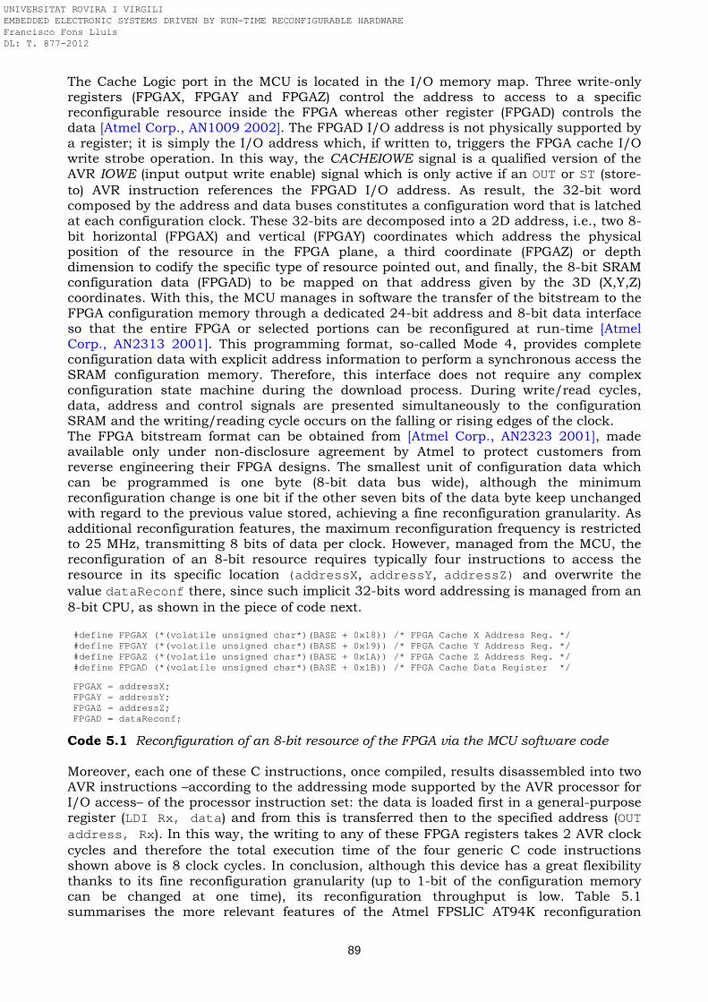
89
The Cache Logic port in the MCU is located in the I/O memory map. Three write-only registers (FPGAX, FPGAY and FPGAZ) control the address to access to a specific reconfigurable resource inside the FPGA whereas other register (FPGAD) controls the data [Atmel Corp., AN1009 2002]. The FPGAD I/O address is not physically supported by a register; it is simply the I/O address which, if written to, triggers the FPGA cache I/O write strobe operation. In this way, the CACHEIOWE signal is a qualified version of the AVR IOWE (input output write enable) signal which is only active if an OUT or ST (store-to) AVR instruction references the FPGAD I/O address. As result, the 32-bit word composed by the address and data buses constitutes a configuration word that is latched at each configuration clock. These 32-bits are decomposed into a 2D address, i.e., two 8-bit horizontal (FPGAX) and vertical (FPGAY) coordinates which address the physical position of the resource in the FPGA plane, a third coordinate (FPGAZ) or depth dimension to codify the specific type of resource pointed out, and finally, the 8-bit SRAM configuration data (FPGAD) to be mapped on that address given by the 3D (X,Y,Z) coordinates. With this, the MCU manages in software the transfer of the bitstream to the FPGA configuration memory through a dedicated 24-bit address and 8-bit data interface so that the entire FPGA or selected portions can be reconfigured at run-time [Atmel Corp., AN2313 2001]. This programming format, so-called Mode 4, provides complete configuration data with explicit address information to perform a synchronous access the SRAM configuration memory. Therefore, this interface does not require any complex configuration state machine during the download process. During write/read cycles, data, address and control signals are presented simultaneously to the configuration SRAM and the writing/reading cycle occurs on the falling or rising edges of the clock. The FPGA bitstream format can be obtained from [Atmel Corp., AN2323 2001], made available only under non-disclosure agreement by Atmel to protect customers from reverse engineering their FPGA designs. The smallest unit of configuration data which can be programmed is one byte (8-bit data bus wide), although the minimum reconfiguration change is one bit if the other seven bits of the data byte keep unchanged with regard to the previous value stored, achieving a fine reconfiguration granularity. As additional reconfiguration features, the maximum reconfiguration frequency is restricted to 25 MHz, transmitting 8 bits of data per clock. However, managed from the MCU, the reconfiguration of an 8-bit resource requires typically four instructions to access the resource in its specific location (addressX, addressY, addressZ) and overwrite the value dataReconf there, since such implicit 32-bits word addressing is managed from an 8-bit CPU, as shown in the piece of code next. #define FPGAX (*(volatile unsigned char*)(BASE + 0x18)) /* FPGA Cache X Address Reg. */ #define FPGAY (*(volatile unsigned char*)(BASE + 0x19)) /* FPGA Cache Y Address Reg. */ #define FPGAZ (*(volatile unsigned char*)(BASE + 0x1A)) /* FPGA Cache Z Address Reg. */ #define FPGAD (*(volatile unsigned char*)(BASE + 0x1B)) /* FPGA Cache Data Register */
FPGAX = addressX; FPGAY = addressY; FPGAZ = addressZ; FPGAD = dataReconf;
Code 5.1 Reconfiguration of an 8-bit resource of the FPGA via the MCU software code Moreover, each one of these C instructions, once compiled, results disassembled into two AVR instructions –according to the addressing mode supported by the AVR processor for I/O access– of the processor instruction set: the data is loaded first in a general-purpose register (LDI Rx, data) and from this is transferred then to the specified address (OUT address, Rx). In this way, the writing to any of these FPGA registers takes 2 AVR clock cycles and therefore the total execution time of the four generic C code instructions shown above is 8 clock cycles. In conclusion, although this device has a great flexibility thanks to its fine reconfiguration granularity (up to 1-bit of the configuration memory can be changed at one time), its reconfiguration throughput is low. Table 5.1 summarises the more relevant features of the Atmel FPSLIC AT94K reconfiguration
UNIVERSITAT ROVIRA I VIRGILI EMBEDDED ELECTRONIC SYSTEMS DRIVEN BY RUN-TIME RECONFIGURABLE HARDWARE Francisco Fons Lluís DL: T. 877-2012
90
controller architecture. In the part IV of this dissertation, some reconfigurable applications are deployed in the AT94K FPSLIC aimed at exploring the performance of this architecture. The main drawback of this PSoC device is, however, its limited size (only 40 Kgates in the AT94K40 device), enabling only the development of small embedded applications. Table 5.1 Atmel AT94K/AT94S FPSLIC reconfiguration controller
DEVICE FAMILY
RECONF. WORD
MAX. RECONF. FREQUENCY
CONFIG. INTERFACE
RECONF. LATENCY
RECONF. GRAIN
AT94K / AT94S
8 bits 25 MHz explicit word address+data 4 memory accesses per data byte 1 bit SRAM
B. Altera Excalibur EPXA SoPC
Altera developed the family of Excalibur system-on-programmable-chip devices which combine a 32-bit RISC ARM9 MCU with an Altera APEX20KE FPGA on a single chip [Altera Corp. HRMEPXA 2002]. The embedded MCU consists of a hard core 32-bit ARM922T processor, on-chip SRAM and dual-port SRAM memories and standard peripherals such as timers, UART or SDRAM controllers, all interconnected through two AMBA AHB buses, AHB1 and AHB2. Besides, external non-volatile and volatile memories (used to store the CPU program and the application data, as well as the FPGA bitstreams) can be linked to the SoPC device through both a SDRAM controller and an expansion bus interface (EBI) internally connected to the AHB buses. All these components compose a typical MCU-based computing platform. In addition to the MCU, an FPGA device is connected to the system through some internal dual-port memories (DPRAM) and also AHB bus interfaces which enable the communication among peripherals of the embedded MCU and custom hardware processors implemented by the designer in the FPGA. In addition, the shared DPRAM allows the logic in the FPGA to interface with the MCU. Besides, a reconfiguration controller is connected to the AHB2 bus to carry out the reconfiguration of the FPGA at run-time. This reconfiguration controller is managed by the ARM9 processor through a set of configuration registers placed in the system memory map. One of these registers is used to buffer the bitstream to the internal FPGA configuration memory. The other control and status configuration registers are connected to the logic of the configuration controller to handle the transfer of the full bitstream from the MCU data buffer register to the FPGA configuration memory adapted to the specific configuration protocol of the APEX20KE device. In this way, the reconfiguration controller provides the configuration port (control, data and status signals) for the specific FPGA interface. The system bitstream contains the configuration data for all the system, i.e., the embedded MCU configuration and its program code, and also the FPGA configuration data. This FPGA admits only a full reconfiguration of the device; a partial reconfiguration is not possible. In this way, the configuration controller takes charge of all the boot process of the Excalibur device, such as configuring the PLLs, the memory map and even the embedded MCU and its cache memories, although the last step related to the FPGA configuration is performed by the embedded MCU itself. In fact, during the reconfiguration, the FPGA is not operative while the MCU keeps in operation and takes charge of the reconfiguration process [Altera Corp., AN187 2003]. The set of configuration registers accessible by the ARM9 CPU to transfer the full bitstream to the configuration memory of the APEX 20KE FPGA are detailed next: The CFG_DATA register is the input buffer through which the reconfiguration
controller receives synchronously the FPGA bitstream, The CFG_CLCK register lets configure the clock frequency used to transfer the
bitstream to the FPGA,
UNIVERSITAT ROVIRA I VIRGILI EMBEDDED ELECTRONIC SYSTEMS DRIVEN BY RUN-TIME RECONFIGURABLE HARDWARE Francisco Fons Lluís DL: T. 877-2012
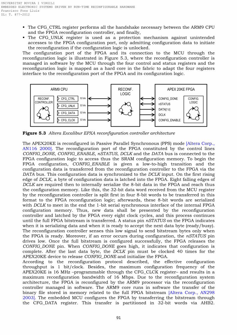
91
ARM9 CPU RECONF. LOGIC
CFG_UNLK
32 bits
CFG_DATA
CFG_CLCK
CFG_CTRL
nSTATUS
DATA[7:0]
DCLK
CONFIG_DONE
APEX 20KE FPGA
32 bits
32 bits
32 bits CONFIG_ENABLE
RECONF. CONTROLLER
CONFIG. LOGIC
The CFG_CTRL register performs all the handshake necessary between the ARM9 CPU and the FPGA reconfiguration controller, and finally,
The CFG_UNLK register is used as a protection mechanism against unintended accesses to the FPGA configuration port, only admitting configuration data to initiate the reconfiguration if the configuration logic is unlocked.
The configuration port of the FPGA and its connection to the MCU through the reconfiguration logic is illustrated in Figure 5.3, where the reconfiguration controller is managed in software by the MCU through the four control and status registers and the reconfiguration logic is mapped as a hard core in the fabric to adapt the four registers interface to the reconfiguration port of the FPGA and its configuration logic.
Figure 5.3 Altera Excalibur EPXA reconfiguration controller architecture The APEX20KE is reconfigured in Passive Parallel Synchronous (PPS) mode [Altera Corp., AN116 2000]. The reconfiguration port of the FPGA constituted by the control lines CONFIG_DONE, CONFIG_ENABLE, nSTATUS, DCLK and the DATA bus is connected to the FPGA configuration logic to access thus the SRAM configuration memory. To begin the FPGA configuration, CONFIG_ENABLE is given a low-to-high transition and the configuration data is transferred from the reconfiguration controller to the FPGA via the DATA bus. This configuration data is synchronized to the DCLK input. On the first rising edge of DCLK, a byte of configuration data is latched into the FPGA. Eight falling edges of DCLK are required then to internally serialize the 8-bit data in the FPGA and reach thus the configuration memory. Like this, the 32-bit data word received from the MCU register by the reconfiguration controller is split first in four 8-bit words to be transferred in this format to the FPGA reconfiguration logic; afterwards, these 8-bit words are serialized with DCLK to meet in the end the 1-bit serial synchronous interface of the internal FPGA configuration memory. Thus, new data shall be presented by the reconfiguration controller and latched by the FPGA every eight clock cycles, and this process continues until the full FPGA bitstream is transferred. A status pin nSTATUS on the FPGA indicates when it is serializing data and when it is ready to accept the next data byte (ready/busy). The reconfiguration controller senses this low signal to send bitstream bytes only when the FPGA is ready. Moreover, if an error occurs during configuration, the nSTATUS pin drives low. Once the full bitstream is configured successfully, the FPGA releases the CONFIG_DONE pin. When CONFIG_DONE goes high, it indicates that configuration is complete. After the last data byte, the DCLK pin must be clocked 40 times for the APEX20KE device to release CONFIG_DONE and initialize the FPGA. According to the reconfiguration protocol described, the effective configuration throughput is 1 bit/clock. Besides, the maximum configuration frequency of the APEX20KE is 16 MHz –programmable through the CFG_CLCK register– and results in a maximum reconfiguration bandwidth of 16 Mbps. Due to the reconfiguration system architecture, the FPGA is reconfigured by the ARM9 processor via the reconfiguration controller managed in software. The ARM9 core runs in software the transfer of the binary file stored in memory related to the full FPGA bitstream [Altera Corp., AN298 2003]. The embedded MCU configures the FPGA by transferring the bitstream through the CFG_DATA register. This transfer is partitioned in 32-bit words via AHB2.
UNIVERSITAT ROVIRA I VIRGILI EMBEDDED ELECTRONIC SYSTEMS DRIVEN BY RUN-TIME RECONFIGURABLE HARDWARE Francisco Fons Lluís DL: T. 877-2012
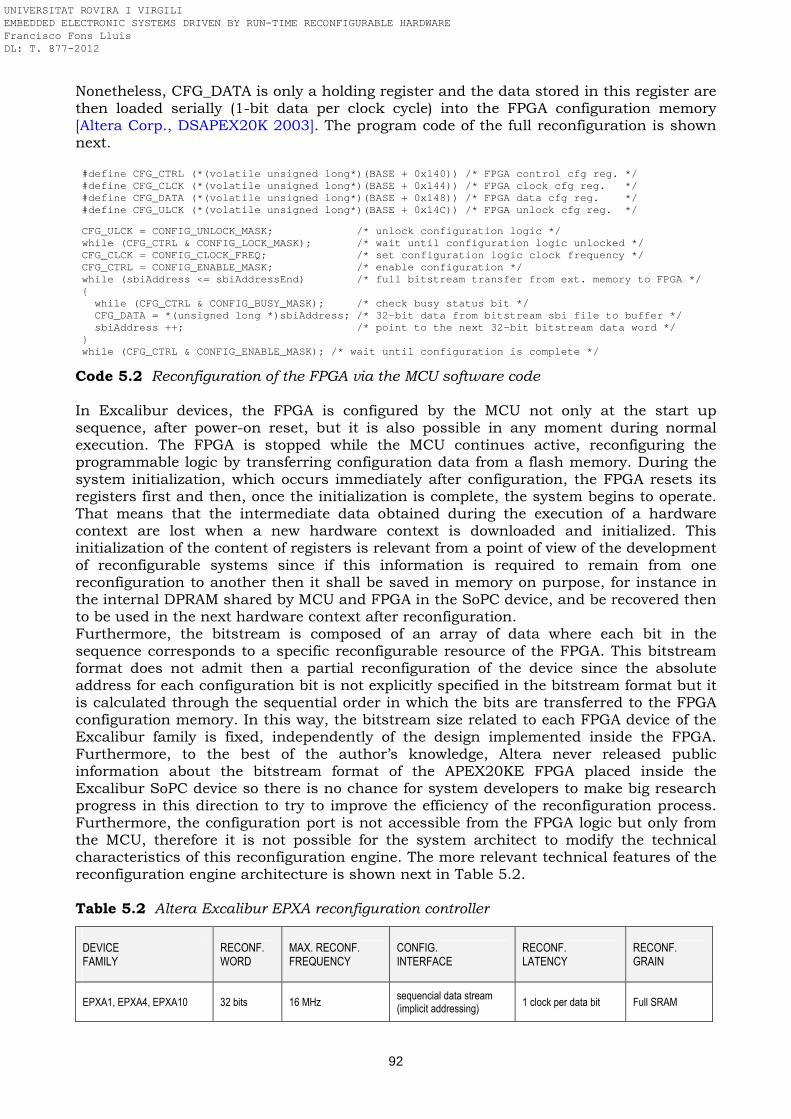
92
Nonetheless, CFG_DATA is only a holding register and the data stored in this register are then loaded serially (1-bit data per clock cycle) into the FPGA configuration memory [Altera Corp., DSAPEX20K 2003]. The program code of the full reconfiguration is shown next. #define CFG_CTRL (*(volatile unsigned long*)(BASE + 0x140)) /* FPGA control cfg reg. */ #define CFG_CLCK (*(volatile unsigned long*)(BASE + 0x144)) /* FPGA clock cfg reg. */ #define CFG_DATA (*(volatile unsigned long*)(BASE + 0x148)) /* FPGA data cfg reg. */ #define CFG_ULCK (*(volatile unsigned long*)(BASE + 0x14C)) /* FPGA unlock cfg reg. */
CFG_ULCK = CONFIG_UNLOCK_MASK; /* unlock configuration logic */ while (CFG_CTRL & CONFIG_LOCK_MASK); /* wait until configuration logic unlocked */ CFG_CLCK = CONFIG_CLOCK_FREQ; /* set configuration logic clock frequency */ CFG_CTRL = CONFIG_ENABLE_MASK; /* enable configuration */ while (sbiAddress <= sbiAddressEnd) /* full bitstream transfer from ext. memory to FPGA */ while (CFG_CTRL & CONFIG_BUSY_MASK); /* check busy status bit */ CFG_DATA = *(unsigned long *)sbiAddress; /* 32-bit data from bitstream sbi file to buffer */ sbiAddress ++; /* point to the next 32-bit bitstream data word */ while (CFG_CTRL & CONFIG_ENABLE_MASK); /* wait until configuration is complete */
Code 5.2 Reconfiguration of the FPGA via the MCU software code In Excalibur devices, the FPGA is configured by the MCU not only at the start up sequence, after power-on reset, but it is also possible in any moment during normal execution. The FPGA is stopped while the MCU continues active, reconfiguring the programmable logic by transferring configuration data from a flash memory. During the system initialization, which occurs immediately after configuration, the FPGA resets its registers first and then, once the initialization is complete, the system begins to operate. That means that the intermediate data obtained during the execution of a hardware context are lost when a new hardware context is downloaded and initialized. This initialization of the content of registers is relevant from a point of view of the development of reconfigurable systems since if this information is required to remain from one reconfiguration to another then it shall be saved in memory on purpose, for instance in the internal DPRAM shared by MCU and FPGA in the SoPC device, and be recovered then to be used in the next hardware context after reconfiguration. Furthermore, the bitstream is composed of an array of data where each bit in the sequence corresponds to a specific reconfigurable resource of the FPGA. This bitstream format does not admit then a partial reconfiguration of the device since the absolute address for each configuration bit is not explicitly specified in the bitstream format but it is calculated through the sequential order in which the bits are transferred to the FPGA configuration memory. In this way, the bitstream size related to each FPGA device of the Excalibur family is fixed, independently of the design implemented inside the FPGA. Furthermore, to the best of the author’s knowledge, Altera never released public information about the bitstream format of the APEX20KE FPGA placed inside the Excalibur SoPC device so there is no chance for system developers to make big research progress in this direction to try to improve the efficiency of the reconfiguration process. Furthermore, the configuration port is not accessible from the FPGA logic but only from the MCU, therefore it is not possible for the system architect to modify the technical characteristics of this reconfiguration engine. The more relevant technical features of the reconfiguration engine architecture is shown next in Table 5.2. Table 5.2 Altera Excalibur EPXA reconfiguration controller
DEVICE FAMILY
RECONF. WORD
MAX. RECONF. FREQUENCY
CONFIG. INTERFACE
RECONF. LATENCY
RECONF. GRAIN
EPXA1, EPXA4, EPXA10
32 bits 16 MHz sequencial data stream (implicit addressing)
1 clock per data bit Full SRAM
UNIVERSITAT ROVIRA I VIRGILI EMBEDDED ELECTRONIC SYSTEMS DRIVEN BY RUN-TIME RECONFIGURABLE HARDWARE Francisco Fons Lluís DL: T. 877-2012
93
The Excalibur device has been used in some application examples conducted in this dissertation, partitioning the application in functional tasks synthesized in specific coprocessors that are performed in the APEX220KE FPGA and reconfigured dynamically by the ARM9 processor. Furthermore, some reconfiguration experiments based on overclocking have been also performed, running the full FPGA reconfiguration at 50 MHz instead of the maximum frequency specified by Altera of 16 MHz, reaching a reconfiguration speed up factor of 3.125 without realizing any failure. Although the Altera Excalibur family is nowadays deprecated, this device remains one of the few commercial SoPCs –along with the Atmel FPSLIC AT94K– which admitted the exploitation of run-time reconfigurable computing already ten years ago, constituted by an ARM processor and an FPGA in the same package. Novel SoC devices recently announced like Altera Cyclone-V and Arria-V SoC FPGAs or Xilinx Zynq-7000 EPPs keep strong similarities with this SoPC device.
5.2.2 Open reconfiguration controller solutions
The reconfigurable platforms overviewed up to now offer a closed, hard-wired solution regarding its reconfiguration engine. Other opposite alternative in commercial FPGAs is to offer the reconfiguration engine as an accessible block, left open to customization after manufacturing the device. Thus, in this case the system architect can design the reconfiguration controller together with the end-user application. This more flexible design approach is possible today with Xilinx FPGA devices, where the reconfiguration controller can be designed as a soft-core IP at post-fabrication. A. Xilinx Virtex/Spartan FPGAs
Xilinx is the FPGA vendor with the longest experience in the exploitation of run-time partial reconfiguration in programmable logic devices. Concerning the reconfiguration granularity of the Xilinx FPGA devices, the grain has been evolving with the launch of new families of devices. As example, the fist Virtex families of FPGA devices (e.g. Virtex-II) are arranged in frames that are tiled about the device. That is, the internal configuration memory is partitioned into vertical segments of one-bit wide called frames. Thus, a frame is the atomic unit of configuration –it is the smallest portion of the configuration memory that can be written to or read from– and all operations must therefore act upon whole configuration frames, while the number and size of frames varies with the device. More recent families of Virtex devices (e.g. Virtex-4) admit a grain composed of a portion (some CLB tall inside the same clock region) of a frame whereas in the Spartan families (e.g. Spartan-3) the grain is increased to a full column, wich is composed of several frames. Thus, depending on the family used, the reconfiguration grain of the programmable logic device is restricted to a specific size. Although a single CLB LUT or flip-flop can be modified, the underlying reconfiguration mechanism does not permit the writing to the configuration memory by addressing a resource lower than the smallest grain. That means that the reconfiguration of a 1-bit resource to change it from 0 to 1 (or 1 to 0) is not possible unless the entire or partial column or frame where this resource is fitted is reconfigured, changing only the target 1-bit resource and overwriting the rest of resources with exactly the same values. As a consequence of this reconfiguration grain, Xilinx FPGAs can be classified in two types from the point of view of partial reconfiguration technology: PR glitchless and non-glitchless devices. Focusing on the devices currently in the market, the PR non-glitchless devices are the Spartan-3 and the extended Spartan-3A/3AN/3A DSP FPGA families. On the contrary, the latest Spartan-6 and the Virtex families Virtex-II, Virtex-II Pro, Virtex-4, Virtex-5 and Virtex-6, in addition to the 7-Series FPGAs and Zynq-7000 EPP devices are built with PR glitchless technology. This is a crucial aspect concerning partial reconfiguration feasibility. PR glitchless technology means that when an FPGA memory cell (logic or routing resource) is reconfigured with the same value (0 or 1) than it has already stored, the memory cell keeps such value constant (0 or 1) before, during and after the reconfiguration, therefore
UNIVERSITAT ROVIRA I VIRGILI EMBEDDED ELECTRONIC SYSTEMS DRIVEN BY RUN-TIME RECONFIGURABLE HARDWARE Francisco Fons Lluís DL: T. 877-2012
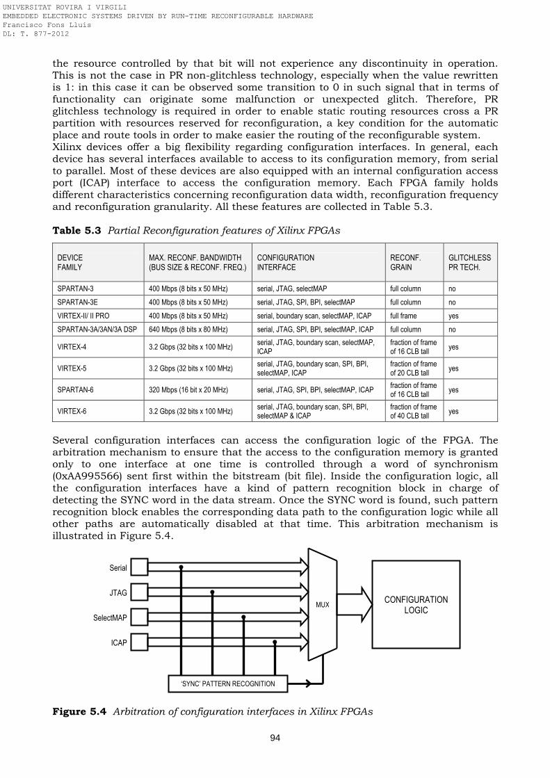
94
CONFIGURATION LOGIC
Serial
‘SYNC’ PATTERN RECOGNITION
MUX
JTAG
SelectMAP
ICAP
the resource controlled by that bit will not experience any discontinuity in operation. This is not the case in PR non-glitchless technology, especially when the value rewritten is 1: in this case it can be observed some transition to 0 in such signal that in terms of functionality can originate some malfunction or unexpected glitch. Therefore, PR glitchless technology is required in order to enable static routing resources cross a PR partition with resources reserved for reconfiguration, a key condition for the automatic place and route tools in order to make easier the routing of the reconfigurable system. Xilinx devices offer a big flexibility regarding configuration interfaces. In general, each device has several interfaces available to access to its configuration memory, from serial to parallel. Most of these devices are also equipped with an internal configuration access port (ICAP) interface to access the configuration memory. Each FPGA family holds different characteristics concerning reconfiguration data width, reconfiguration frequency and reconfiguration granularity. All these features are collected in Table 5.3. Table 5.3 Partial Reconfiguration features of Xilinx FPGAs
DEVICE FAMILY
MAX. RECONF. BANDWIDTH (BUS SIZE & RECONF. FREQ.)
CONFIGURATION INTERFACE
RECONF. GRAIN
GLITCHLESS PR TECH.
SPARTAN-3 400 Mbps (8 bits x 50 MHz) serial, JTAG, selectMAP full column no
SPARTAN-3E 400 Mbps (8 bits x 50 MHz) serial, JTAG, SPI, BPI, selectMAP full column no
VIRTEX-II/ II PRO 400 Mbps (8 bits x 50 MHz) serial, boundary scan, selectMAP, ICAP full frame yes
SPARTAN-3A/3AN/3A DSP 640 Mbps (8 bits x 80 MHz) serial, JTAG, SPI, BPI, selectMAP, ICAP full column no
VIRTEX-4 3.2 Gbps (32 bits x 100 MHz) serial, JTAG, boundary scan, selectMAP, ICAP
fraction of frame of 16 CLB tall
yes
VIRTEX-5 3.2 Gbps (32 bits x 100 MHz) serial, JTAG, boundary scan, SPI, BPI, selectMAP, ICAP
fraction of frame of 20 CLB tall
yes
SPARTAN-6 320 Mbps (16 bit x 20 MHz) serial, JTAG, SPI, BPI, selectMAP, ICAP fraction of frame of 16 CLB tall
yes
VIRTEX-6 3.2 Gbps (32 bits x 100 MHz) serial, JTAG, boundary scan, SPI, BPI, selectMAP & ICAP
fraction of frame of 40 CLB tall
yes
Several configuration interfaces can access the configuration logic of the FPGA. The arbitration mechanism to ensure that the access to the configuration memory is granted only to one interface at one time is controlled through a word of synchronism (0xAA995566) sent first within the bitstream (bit file). Inside the configuration logic, all the configuration interfaces have a kind of pattern recognition block in charge of detecting the SYNC word in the data stream. Once the SYNC word is found, such pattern recognition block enables the corresponding data path to the configuration logic while all other paths are automatically disabled at that time. This arbitration mechanism is illustrated in Figure 5.4.
Figure 5.4 Arbitration of configuration interfaces in Xilinx FPGAs
UNIVERSITAT ROVIRA I VIRGILI EMBEDDED ELECTRONIC SYSTEMS DRIVEN BY RUN-TIME RECONFIGURABLE HARDWARE Francisco Fons Lluís DL: T. 877-2012
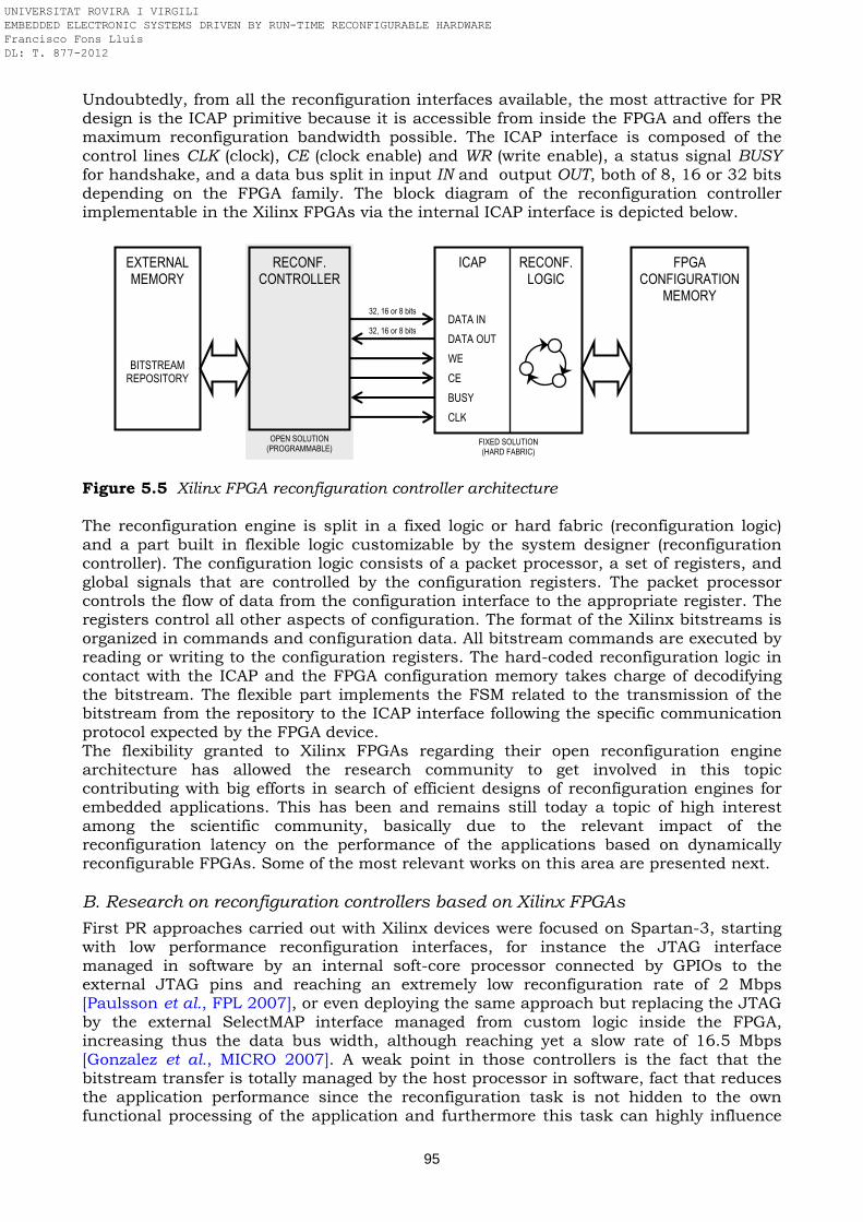
95
RECONF. CONTROLLER
ICAP
32, 16 or 8 bits
DATA OUT
WE
CE
DATA IN
FPGA CONFIGURATION
MEMORY
BUSY
RECONF. LOGIC
CLK
32, 16 or 8 bits
EXTERNAL MEMORY
BITSTREAM REPOSITORY
OPEN SOLUTION (PROGRAMMABLE)
FIXED SOLUTION (HARD FABRIC)
Undoubtedly, from all the reconfiguration interfaces available, the most attractive for PR design is the ICAP primitive because it is accessible from inside the FPGA and offers the maximum reconfiguration bandwidth possible. The ICAP interface is composed of the control lines CLK (clock), CE (clock enable) and WR (write enable), a status signal BUSY for handshake, and a data bus split in input IN and output OUT, both of 8, 16 or 32 bits depending on the FPGA family. The block diagram of the reconfiguration controller implementable in the Xilinx FPGAs via the internal ICAP interface is depicted below.
Figure 5.5 Xilinx FPGA reconfiguration controller architecture The reconfiguration engine is split in a fixed logic or hard fabric (reconfiguration logic) and a part built in flexible logic customizable by the system designer (reconfiguration controller). The configuration logic consists of a packet processor, a set of registers, and global signals that are controlled by the configuration registers. The packet processor controls the flow of data from the configuration interface to the appropriate register. The registers control all other aspects of configuration. The format of the Xilinx bitstreams is organized in commands and configuration data. All bitstream commands are executed by reading or writing to the configuration registers. The hard-coded reconfiguration logic in contact with the ICAP and the FPGA configuration memory takes charge of decodifying the bitstream. The flexible part implements the FSM related to the transmission of the bitstream from the repository to the ICAP interface following the specific communication protocol expected by the FPGA device. The flexibility granted to Xilinx FPGAs regarding their open reconfiguration engine architecture has allowed the research community to get involved in this topic contributing with big efforts in search of efficient designs of reconfiguration engines for embedded applications. This has been and remains still today a topic of high interest among the scientific community, basically due to the relevant impact of the reconfiguration latency on the performance of the applications based on dynamically reconfigurable FPGAs. Some of the most relevant works on this area are presented next. B. Research on reconfiguration controllers based on Xilinx FPGAs
First PR approaches carried out with Xilinx devices were focused on Spartan-3, starting with low performance reconfiguration interfaces, for instance the JTAG interface managed in software by an internal soft-core processor connected by GPIOs to the external JTAG pins and reaching an extremely low reconfiguration rate of 2 Mbps [Paulsson et al., FPL 2007], or even deploying the same approach but replacing the JTAG by the external SelectMAP interface managed from custom logic inside the FPGA, increasing thus the data bus width, although reaching yet a slow rate of 16.5 Mbps [Gonzalez et al., MICRO 2007]. A weak point in those controllers is the fact that the bitstream transfer is totally managed by the host processor in software, fact that reduces the application performance since the reconfiguration task is not hidden to the own functional processing of the application and furthermore this task can highly influence
UNIVERSITAT ROVIRA I VIRGILI EMBEDDED ELECTRONIC SYSTEMS DRIVEN BY RUN-TIME RECONFIGURABLE HARDWARE Francisco Fons Lluís DL: T. 877-2012
96
the application scheduling. This reconfiguration time, usually carried out in one shot –without interruptions in between– to accelerate thus the swapping of PR modules, could provoke some difficulties to fit a long non-preemptive task devoted to reconfiguration in the scheduling of applications like digital signal processing that demand a cyclic signal sampling/computation at high frequencies. Just for this reason, intended to minimize the impact of the reconfiguration over the application processing itself and not to degrade the CPU performance with excessive additional workload, it results advisable to design a master reconfiguration processor to manage all the transfer by itself, freeing thus the system CPU. All these advances are applied in [Bayar and Yurdakul, HiPEAC 2008], still under Spartan-3, based on a stand-alone hardware reconfiguration controller which downloads the partial bitstream via the SelectMAP interface. Although it reaches the maximum reconfiguration throughput of Spartan-3 FPGAs (8-bit data at 50 MHz, i.e. 400 Mbps), the main drawback of this solution is that the partial bitstream has to be preloaded in BRAM (internal RAM blocks of the FPGA) because the controller retrieves the data from there. This fact restricts this solution to extremely small partial bitstreams given that, in general, the amount of RAM blocks available inside a FPGA is very limited. Hence, this solution is only suitable for small PR regions. Another approach based on Spartan-3 is presented in [Cantó et al., FPL 2009] where it is developed a custom reconfiguration controller connected to the LMB-EMC bus. This controller retrieves 32-bit words from an external SRAM or Flash memory using a LMB-EMC memory controller and drives the 8-bit SelectMAP interface under a system clock of 40 MHz, reaching a reconfiguration throughput of 319.8 Mbps. Apart from Spartan-3 devices, other works have been conducted on Virtex-II Pro devices. A NoC system equipped with a custom ICAP-based configuration controller under Virtex-II Pro is presented in [Möller et al., ReCoSoC 2007], reaching a reconfiguration throughput of around 80 Mbps. This reconfiguration throughput is achieved also in [Bomel et al., ARCS 2009] with an embedded application running over Ethernet at 100 Mbps where the reconfiguration controller retrieve from remote servers the partial bitstreams to be downloaded in the FPGA. This solution is prototyped in a Virtex-II Pro device running at 100 MHz and the reconfiguration controller is implemented in software by the PPC405 core and supported by DMA transfers. Both the processor and the Ethernet controller are connected to the CoreConnect PLB bus and from there the bitstream is bridged to the OPB bus where the ICAP interface resides. Another work based on Virtex-II Pro and detailed in [Van der Bok et al., ProRISC 2007] concerns to the implementation of an ICAP-based reconfiguration controller able to reconfigure a PRR at its maximum throughput of 400 Mbps (8-bit data interface operating at 50 MHz). However, such reconfiguration controller is designed in the way that it is connected to the repository of reconfigurable bitstreams in an exclusive mode, i.e., an external memory device is used as a dedicated resource connected only to the reconfiguration controller by means of a specific memory controller –so-called partial reconfiguration management unit (PRMU) – and connected to the external memory. The fact of using a dedicated memory instead of a shared one to store the partial bitstreams can notoriously increase the cost of the embedded solution since other processors in the system, e.g. the CPU, do not have access to that data source and probably will require access to extensive data, demanding thus the presence a second memory source in the system. Apart from this drawback, as advantage, the dedicated bus to connect the reconfiguration controller to the memory releases the processor bus, freeing it to other processors. Going on with the overview of Virtex-II Pro based reconfiguration controllers, a master CoreConnect PLB ICAP controller is developed in [Claus et al., IPDPS 2007]. It is equipped with DMA capability to work independently of the CPU. The PLB and ICAP are clocked at 100 MHz. This ICAP overclocking is possible by using a simple handshake protocol based on the BUSY signal of the ICAP. This signal informs when it is possible to flow data through the ICAP port. When the ICAP is busy, it is necessary to insert wait states as a result of overclocking the ICAP above its specified frequency. In these conditions, it was possible to achieve an effective throughput of 760 Mbps.
UNIVERSITAT ROVIRA I VIRGILI EMBEDDED ELECTRONIC SYSTEMS DRIVEN BY RUN-TIME RECONFIGURABLE HARDWARE Francisco Fons Lluís DL: T. 877-2012
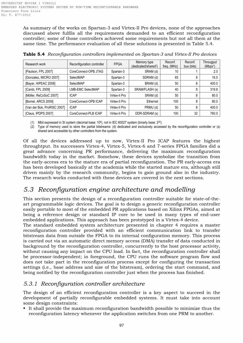
97
As summary of the works on Spartan-3 and Virtex-II Pro devices, none of the approaches discussed above fulfils all the requirements demanded to an efficient reconfiguration controller; some of those controllers achieved some requirements but not all them at the same time. The performance evaluation of all these solutions is presented in Table 5.4. Table 5.4 Reconfiguration controllers implemented on Spartan-3 and Virtex-II Pro devices
Research work Reconfiguration controller FPGA Memory type
(dedicated/shared2) Reconf.
freq. (MHz) Reconf.
bus (bits) Througput (Mbps1)
[Paulson, FPL 2007] CoreConnect-OPB JTAG Spartan-3 SRAM (d) 10 1 2.0
[Gonzalez, MICRO 2007] SelectMAP Spartan-3 SDRAM (d) 65 8 16.5
[Bayar, HiPEAC 2008] SelectMAP Spartan-3 BRAM (d) 50 8 400.0
[Cantó, FPL 2009] LMB-EMC SelectMAP Spartan-3 SRAM/FLASH (s) 40 8 319.8
[Möller, ReCoSoC 2007] ICAP Virtex-II Pro SRAM (d) 50 8 80.0
[Bomel, ARCS 2009] CoreConnect-OPB ICAP Virtex-II Pro Ethernet 100 8 80.0
[Van der Bok, ProRISC 2007] ICAP Virtex-II Pro PRMU (d) 50 8 400.0
[Claus, IPDPS 2007] CoreConnect-PLB ICAP Virtex-II Pro DDR-SDRAM (s) 100 32 760.0
(1) Mbit expressed in SI system (decimal base: 106), not in IEC 60027 system (binarly base: 220). (2) Type of memory used to store the partial bitstreams: (d) dedicated and exclusively accessed by the reconfiguration controller or (s)
shared and accessible by other controllers from the system. Of all the devices addressed up to now, Virtex-II Pro ICAP features the highest throughtput. Its successors Virtex-4, Virtex-5, Virtex-6 and 7-series FPGA families did a great advance concerning PR performance, delivering the maximum reconfiguration bandwidth today in the market. Somehow, these devices symbolize the transition from the early-access era to the mature era of partial reconfiguration. The PR early-access era has been developed basically at the academia while the started mature era, although still driven mainly by the research community, begins to gain ground also in the industry. The research works conducted with these devices are covered in the next sections.
5.3 Reconfiguration engine architecture and modelling
This section presents the design of a reconfiguration controller suitable for state-of-the-art programmable logic devices. The goal is to design a generic reconfiguration controller easily portable to most of the embedded PR applications based on Xilinx FPGAs, aimed at being a reference design or standard IP core to be used in many types of end-user embedded applications. This approach has been prototyped in a Virtex-4 device. The standard embedded system architecture presented in chapter 4 requires a master reconfiguration controller provided with an efficient communication link to transfer bitstream data from outside the FPGA to its internal configuration memory. This process is carried out via an automatic direct memory access (DMA) transfer of data conducted in background by the reconfiguration controller, concurrently to the host processor activity, without causing any impact on the CPU load. In fact, the reconfiguration controller shall be processor-independent; in foreground, the CPU runs the software program flow and does not take part in the reconfiguration process except for configuring the transaction settings (i.e., base address and size of the bitstream), ordering the start command, and being notified by the reconfiguration controller just when the process has finished.
5.3.1 Reconfiguration controller architecture
The design of an efficient reconfiguration controller is a key aspect to succeed in the development of partially reconfigurable embedded systems. It must take into account some design constraints: It shall provide the maximum reconfiguration bandwidth possible to minimize thus the
reconfiguration latency whenever the application switches from one PRM to another.
UNIVERSITAT ROVIRA I VIRGILI EMBEDDED ELECTRONIC SYSTEMS DRIVEN BY RUN-TIME RECONFIGURABLE HARDWARE Francisco Fons Lluís DL: T. 877-2012
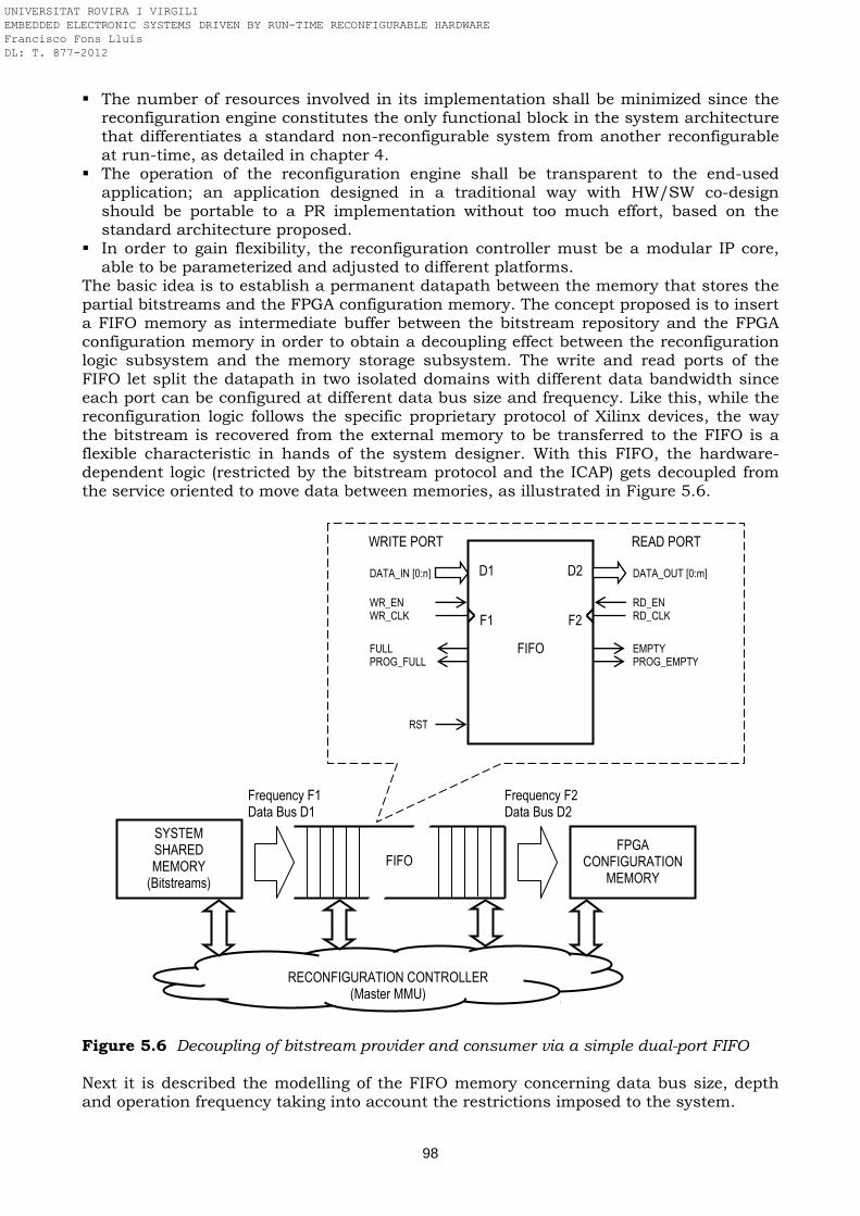
98
The number of resources involved in its implementation shall be minimized since the reconfiguration engine constitutes the only functional block in the system architecture that differentiates a standard non-reconfigurable system from another reconfigurable at run-time, as detailed in chapter 4.
The operation of the reconfiguration engine shall be transparent to the end-used application; an application designed in a traditional way with HW/SW co-design should be portable to a PR implementation without too much effort, based on the standard architecture proposed.
In order to gain flexibility, the reconfiguration controller must be a modular IP core, able to be parameterized and adjusted to different platforms.
The basic idea is to establish a permanent datapath between the memory that stores the partial bitstreams and the FPGA configuration memory. The concept proposed is to insert a FIFO memory as intermediate buffer between the bitstream repository and the FPGA configuration memory in order to obtain a decoupling effect between the reconfiguration logic subsystem and the memory storage subsystem. The write and read ports of the FIFO let split the datapath in two isolated domains with different data bandwidth since each port can be configured at different data bus size and frequency. Like this, while the reconfiguration logic follows the specific proprietary protocol of Xilinx devices, the way the bitstream is recovered from the external memory to be transferred to the FIFO is a flexible characteristic in hands of the system designer. With this FIFO, the hardware-dependent logic (restricted by the bitstream protocol and the ICAP) gets decoupled from the service oriented to move data between memories, as illustrated in Figure 5.6.
Figure 5.6 Decoupling of bitstream provider and consumer via a simple dual-port FIFO Next it is described the modelling of the FIFO memory concerning data bus size, depth and operation frequency taking into account the restrictions imposed to the system.
Frequency F1 Data Bus D1
Frequency F2 Data Bus D2
FPGA CONFIGURATION
MEMORY
SYSTEM SHARED MEMORY
(Bitstreams)
FIFO
RECONFIGURATION CONTROLLER (Master MMU)
WR_CLK RD_EN WR_EN RD_CLK
EMPTY FULL PROG_EMPTY PROG_FULL
RST
DATA_IN [0:n] DATA_OUT [0:m]
FIFO
WRITE PORT READ PORT
D2
F2
D1
F1
UNIVERSITAT ROVIRA I VIRGILI EMBEDDED ELECTRONIC SYSTEMS DRIVEN BY RUN-TIME RECONFIGURABLE HARDWARE Francisco Fons Lluís DL: T. 877-2012
99
5.3.2 Analytical model formulation
The decoupling of data bandwidth between the write port and the read port of the FIFO memory is achieved by designing both parameters –data bus size and operation frequency– of each port individually, according to particular restrictions imposed to every side of the FIFO, i.e., the memory storage and the reconfiguration logic itself. The side related to the bistreams repository, which operates the write port of the FIFO, is usually managed by a memory management unit (MMU). We use this acronym to refer to terms of this part. The other side affected by the read port of the FIFO involves to the configuration logic; likewise, the parameters related to this side will be designated by the acronym CFG in the following mathematical development. In a first formulation, it is presented the study of throughput aimed at minimizing the reconfiguration time. A. Minimum reconfiguration time
Given a module described in HDL to implement a specific functionality in programmable logic, once it is mapped in a certain FPGA technology and placed and routed in a specific PRR, this PRM is abstracted in a binary file or bitstream. The resultant length of this bitstream depends on the area bounded by the PRR (i.e., type and number of programmable resources affected) and on the complexity of the PRM to synthesize such functionality on those specific resources of the FPGA. Compilation tools perform all this process automatically to convert the HDL code in binary data. This bistream must be as short of possible to optimise thus two metrics: memory space and reconfiguration time. Given a PRM defined by a partial bitstream of n bits, its reconfiguration into a specific PRR consists in transferring the n bits to the configuration logic. The configuration logic decodifies the n bits of the bitstream –usually decomposed in instructions, addresses and configuration data– to store thus each configuration bit into the specific address of the FPGA configuration memory. In order to minimize the reconfiguration time, the transfer of data to the configuration logic must be performed at the maximum throughput admitted, which is obtained when combining the maximum bandwidth (i.e., maximum operation frequency f and maximum data bus width w of the configuration logic interface) and furthermore transferring the n bits continuously at one word per clock until the end, without interrupting this process by inserting wait states in between. Thus, given a FIFO parameterized by the features shown next where the write port is connected to the MMU and the read port is connected to the configuration logic (CFG): Write Port
[ ][ ]Hz
Tffrequency
bitswword
MMUMMU
MMU
1==
= (5.1)
Read Port
[ ][ ]Hz
Tffrequency
bitswword
CFGCFG
CFG
1==
= (5.2)
in order to achieve the minimum reconfiguration latency, fCFG and wCFG shall match both the respective maximum values admitted. Additionally, once the bitstream transaction starts and the first word is received in the FIFO, the data flow must continue until the n bits are transferred to the configuration logic. This condition implies that the FIFO memory must not get empty until the transfer ends, so that the read port is continuously sourcing data to the configuration logic. This condition can be expressed in the form that the write port of the FIFO (MMU domain) shall provide a throughput or effective
UNIVERSITAT ROVIRA I VIRGILI EMBEDDED ELECTRONIC SYSTEMS DRIVEN BY RUN-TIME RECONFIGURABLE HARDWARE Francisco Fons Lluís DL: T. 877-2012
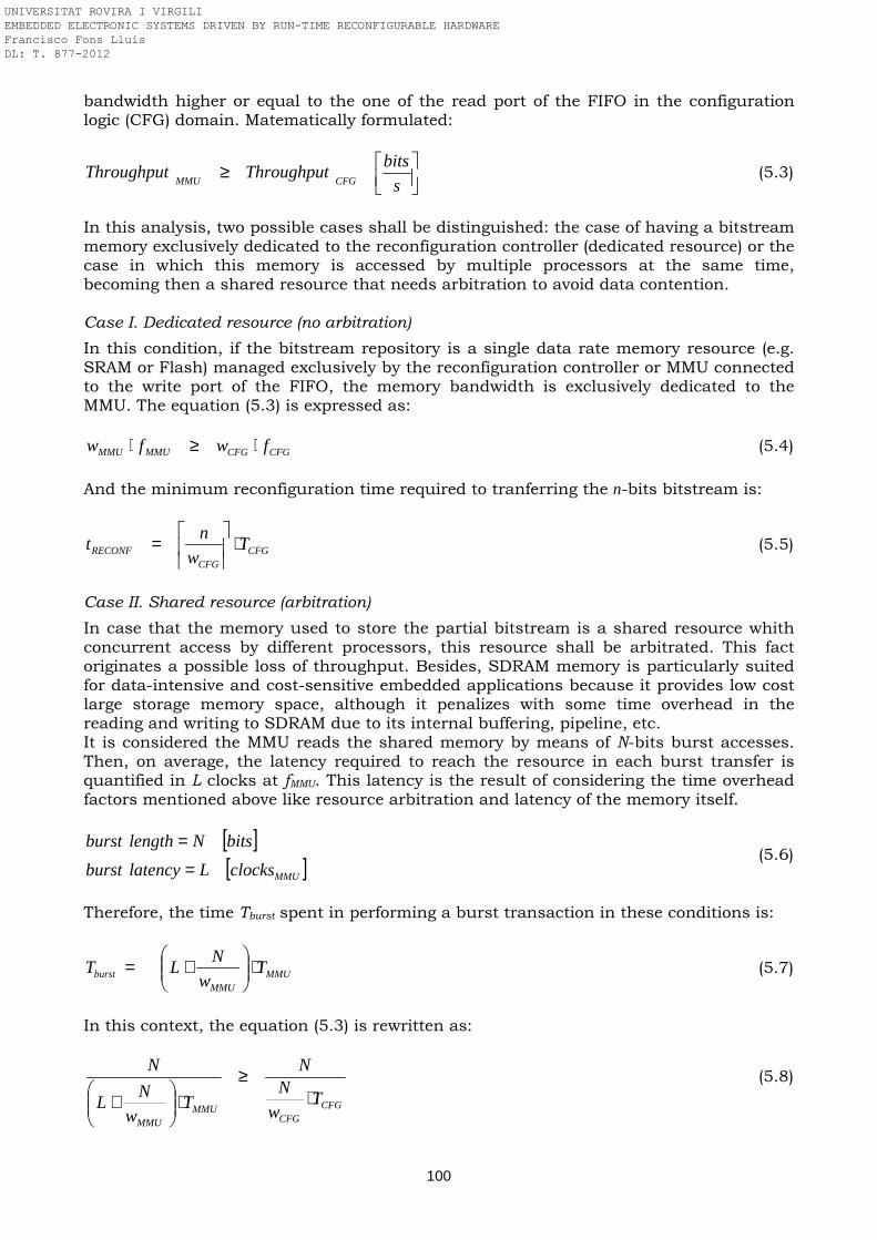
100
bandwidth higher or equal to the one of the read port of the FIFO in the configuration logic (CFG) domain. Matematically formulated:
≥s
bitsThroughputThroughput
CFGMMU (5.3)
In this analysis, two possible cases shall be distinguished: the case of having a bitstream memory exclusively dedicated to the reconfiguration controller (dedicated resource) or the case in which this memory is accessed by multiple processors at the same time, becoming then a shared resource that needs arbitration to avoid data contention. Case I. Dedicated resource (no arbitration)
In this condition, if the bitstream repository is a single data rate memory resource (e.g. SRAM or Flash) managed exclusively by the reconfiguration controller or MMU connected to the write port of the FIFO, the memory bandwidth is exclusively dedicated to the MMU. The equation (5.3) is expressed as:
CFGCFGMMUMMU fwfw ⋅≥⋅ (5.4)
And the minimum reconfiguration time required to tranferring the n-bits bitstream is:
CFGCFG
RECONF Tw
nt ⋅
= (5.5)
Case II. Shared resource (arbitration)
In case that the memory used to store the partial bitstream is a shared resource whith concurrent access by different processors, this resource shall be arbitrated. This fact originates a possible loss of throughput. Besides, SDRAM memory is particularly suited for data-intensive and cost-sensitive embedded applications because it provides low cost large storage memory space, although it penalizes with some time overhead in the reading and writing to SDRAM due to its internal buffering, pipeline, etc. It is considered the MMU reads the shared memory by means of N-bits burst accesses. Then, on average, the latency required to reach the resource in each burst transfer is quantified in L clocks at fMMU. This latency is the result of considering the time overhead factors mentioned above like resource arbitration and latency of the memory itself.
[ ][ ]MMUclocksLlatencyburst
bitsNlengthburst
==
(5.6)
Therefore, the time Tburst spent in performing a burst transaction in these conditions is:
MMUMMU
burst Tw
NLT ⋅
+= (5.7)
In this context, the equation (5.3) is rewritten as:
CFGCFG
MMUMMU
Tw
NN
Tw
NL
N
⋅≥
⋅
+
(5.8)
UNIVERSITAT ROVIRA I VIRGILI EMBEDDED ELECTRONIC SYSTEMS DRIVEN BY RUN-TIME RECONFIGURABLE HARDWARE Francisco Fons Lluís DL: T. 877-2012
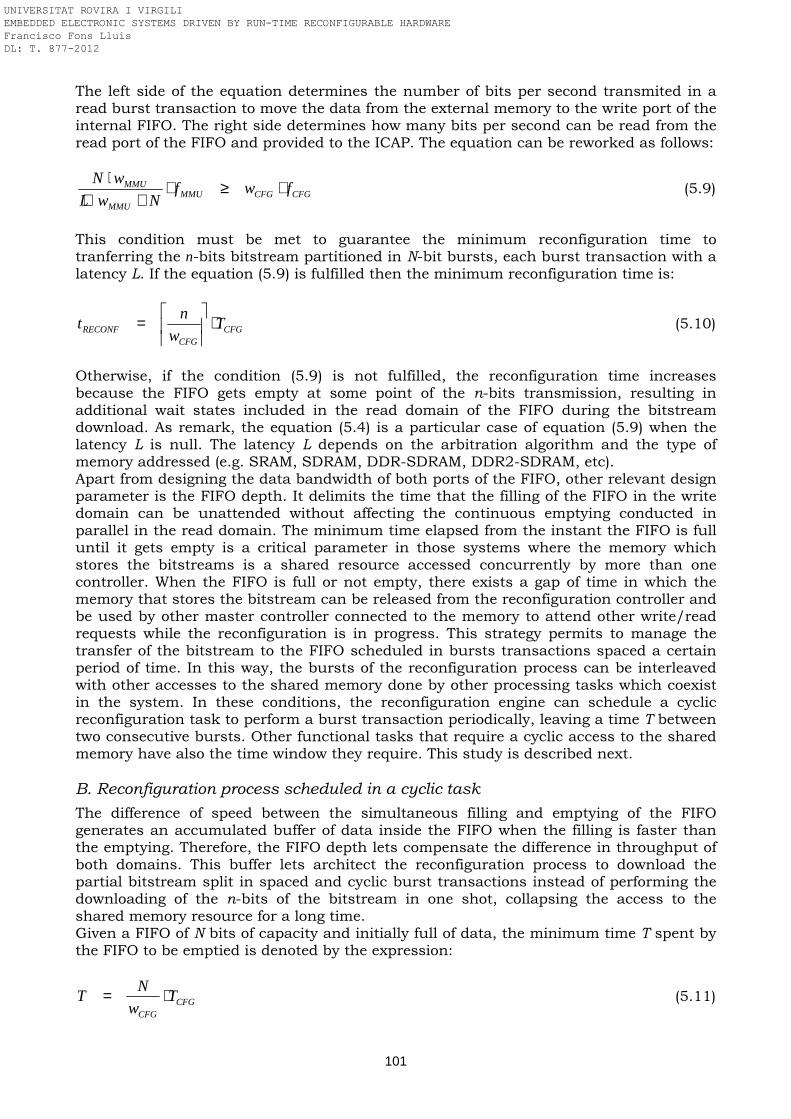
101
The left side of the equation determines the number of bits per second transmited in a read burst transaction to move the data from the external memory to the write port of the internal FIFO. The right side determines how many bits per second can be read from the read port of the FIFO and provided to the ICAP. The equation can be reworked as follows:
CFGCFGMMUMMU
MMU fwfNwL
wN ⋅≥⋅+⋅
⋅ (5.9)
This condition must be met to guarantee the minimum reconfiguration time to tranferring the n-bits bitstream partitioned in N-bit bursts, each burst transaction with a latency L. If the equation (5.9) is fulfilled then the minimum reconfiguration time is:
CFGCFG
RECONF Tw
nt ⋅
= (5.10)
Otherwise, if the condition (5.9) is not fulfilled, the reconfiguration time increases because the FIFO gets empty at some point of the n-bits transmission, resulting in additional wait states included in the read domain of the FIFO during the bitstream download. As remark, the equation (5.4) is a particular case of equation (5.9) when the latency L is null. The latency L depends on the arbitration algorithm and the type of memory addressed (e.g. SRAM, SDRAM, DDR-SDRAM, DDR2-SDRAM, etc). Apart from designing the data bandwidth of both ports of the FIFO, other relevant design parameter is the FIFO depth. It delimits the time that the filling of the FIFO in the write domain can be unattended without affecting the continuous emptying conducted in parallel in the read domain. The minimum time elapsed from the instant the FIFO is full until it gets empty is a critical parameter in those systems where the memory which stores the bitstreams is a shared resource accessed concurrently by more than one controller. When the FIFO is full or not empty, there exists a gap of time in which the memory that stores the bitstream can be released from the reconfiguration controller and be used by other master controller connected to the memory to attend other write/read requests while the reconfiguration is in progress. This strategy permits to manage the transfer of the bitstream to the FIFO scheduled in bursts transactions spaced a certain period of time. In this way, the bursts of the reconfiguration process can be interleaved with other accesses to the shared memory done by other processing tasks which coexist in the system. In these conditions, the reconfiguration engine can schedule a cyclic reconfiguration task to perform a burst transaction periodically, leaving a time T between two consecutive bursts. Other functional tasks that require a cyclic access to the shared memory have also the time window they require. This study is described next. B. Reconfiguration process scheduled in a cyclic task
The difference of speed between the simultaneous filling and emptying of the FIFO generates an accumulated buffer of data inside the FIFO when the filling is faster than the emptying. Therefore, the FIFO depth lets compensate the difference in throughput of both domains. This buffer lets architect the reconfiguration process to download the partial bitstream split in spaced and cyclic burst transactions instead of performing the downloading of the n-bits of the bitstream in one shot, collapsing the access to the shared memory resource for a long time. Given a FIFO of N bits of capacity and initially full of data, the minimum time T spent by the FIFO to be emptied is denoted by the expression:
CFGCFG
Tw
NT ⋅= (5.11)
UNIVERSITAT ROVIRA I VIRGILI EMBEDDED ELECTRONIC SYSTEMS DRIVEN BY RUN-TIME RECONFIGURABLE HARDWARE Francisco Fons Lluís DL: T. 877-2012

102
This time delimits the period of the task scheduled to perform the downloading of a n-bits bitstream organized in burst transactions of N-bits size and freeing up the memory access after each burst to other resources accessing the shared memory, with a latency L to access the shared resource. The free time Tfree between two consecutive bursts is obtained from equations (5.7) and (5.11) as follows:
MMUMMU
CFGCFG
burstfree Tw
NLT
w
NTTT ⋅
+−⋅=−= (5.12)
This free time of the shared resource can be used by other master controllers in the systems to access the memory while the reconfiguration is conducted. This interleaving of tasks is interesting in order to hide the reconfiguration process of one PRM while other tasks are processed concurrently. Furthermore, this reconfiguration can be hidden by other hardware tasks processed in other PRRs while one of the PRRs is reconfigured.
5.3.3 System integration and proof of feasibility
The reconfiguration controller modelled in the previous section has been prototyped in a Xilinx Virtex-4 FPGA. The platform used is the Xilinx ML401 evaluation board composed of the XC4VLX25 FPGA. Following the minimalist system architecture proposed in chapter 4, the embedded system is composed of a host processor (MicroBlaze sof-core), the reconfiguration controller and a PR region. Besides, a DDR-SDRAM chip is managed by a MPMC synthesized in the FPGA connected to four buses: a 64-bit Native Port Interface (NPI), a 32-bit PLBv46, and two Xilinx Cache Link (XCL) buses, where the system designer can define the priority given to each of the buses [Xilinx Inc., DS643 2008]. The NPI is connected to the master MMU. The PLBv46 is the multiprocessor bus of the system, used by the host processor and its peripherals. The other two XCL buses are oriented to fast instructions and data caches of the host processor, respectively. These caches are built with internal RAM blocks of the FPGA. Although the system also has Flash memory, the system uses DDR-SDRAM as repository of bitstreams since, in a generic case, the bitstream can come also from an external communication link in case of a remote system update. In this way, it is considered that the bitstream will be moved to the DDR-SDRAM before starting the reconfiguration process. This DDR-SDRAM memory stores the program code, the settings or application data required by the different controllers of the system and the partial bitstreams. Therefore, this memory is a shared resource accessible by the host processor, the PRMs and the reconfiguration engine at any time. Due to this reason, it is connected to a MPMC from which it can be accessed either by the host processor –from the PLBv46 system bus or the XCL buses– or by the reconfiguration controller or PRM – via the NPI bus connected to a master MMU specifically designed for establishing a fast link between the external DDR-SDRAM repository and both the ICAP primitive and the PRR. The block diagram of the system is shown in Figure 5.7. The designed master MMU handles the data transaction between the DDR-SDRAM memory and up to three internal FIFOs, one connected to the FPGA configuration memory and the others to the PRR, via the NPI protocol. The NPI is configured with a 64-bits data bus. This 64-bit data bus is connected to the write port of the FIFO inserted in the datapath of the FPGA configuration memory. The counterpart read port of such FIFO uses a data bus length of 32-bit since this is the maximum length admitted by the ICAP primitive in Virtex-4 devices. Regarding operation frequencies, both write and read ports of the FIFO, i.e. NPI and ICAP sides, work at 100 MHz, although the NPI side could work at a higher rate if necessary. The maximum frequency admitted by the ICAP interface is 100 MHz. Concerning capacity, the FIFO has a depth of 1024 words of 32 bits, delimited basically by the size (total RAM bits) and flexible geometry (width and depth) admitted by the RAM blocks in the Virtex-4 technology.
UNIVERSITAT ROVIRA I VIRGILI EMBEDDED ELECTRONIC SYSTEMS DRIVEN BY RUN-TIME RECONFIGURABLE HARDWARE Francisco Fons Lluís DL: T. 877-2012
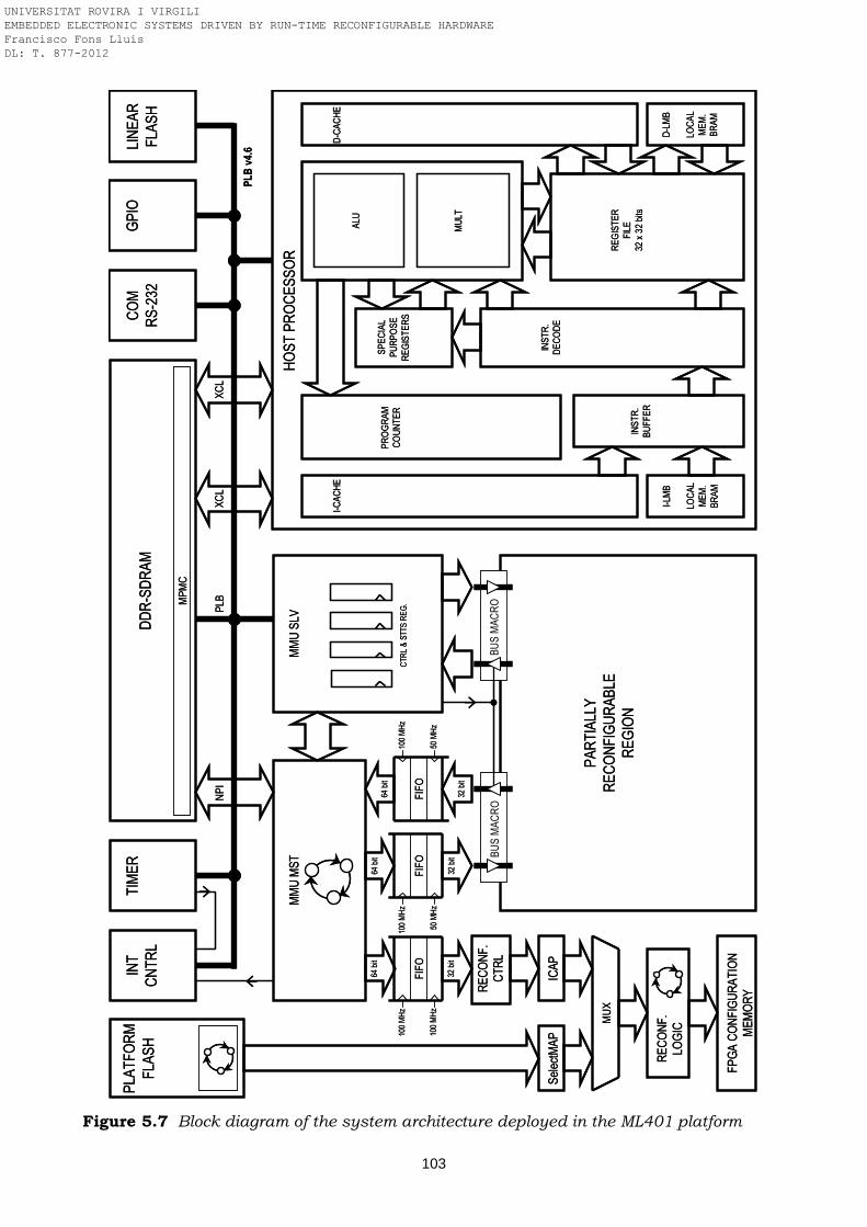
103
Figure 5.7 Block diagram of the system architecture deployed in the ML401 platform
PLAT
FOR
M
FLAS
H
PLB
HO
ST P
RO
CES
SOR
MM
U M
ST
Sele
ctM
AP
FPG
A C
ON
FIG
UR
ATIO
NM
EMO
RY
FIFO
FIFO
FIFO
PAR
TIAL
LYR
ECO
NFI
GU
RAB
LER
EGIO
N
MM
U S
LV
NPI
DD
R-S
DR
AM
MPM
C
INT
CN
TRL
TIM
ERC
OM
RS-
232
GPI
OLI
NEA
R
FLAS
H
REC
ON
F.
LOG
IC
MU
X
ICAP
REC
ON
F.C
TRL
PLB v4.6
CTR
L &
STT
S R
EG
.
BUS
MAC
RO
BUS
MAC
RO
100
MH
z
100
MH
z
100
MH
z
50 M
Hz
100
MH
z
50 M
Hz
64 b
it64
bit
64 b
it
32 b
it32
bit
32 b
it
XCL
XCL
I-CAC
HE
PRO
GR
AM
CO
UN
TER
INST
R.
BUFF
ER
INST
R.
DEC
OD
E
REG
ISTE
RFI
LE32
x 3
2 bi
ts
ALU
MU
LT
SPEC
IAL
PUR
POSE
REG
ISTE
RS
D-L
MB
LOC
ALM
EM.
BRAM
D-C
ACH
E
I-LM
B
LOC
ALM
EM.
BRAM
UNIVERSITAT ROVIRA I VIRGILI EMBEDDED ELECTRONIC SYSTEMS DRIVEN BY RUN-TIME RECONFIGURABLE HARDWARE Francisco Fons Lluís DL: T. 877-2012
104
In order to reduce the transfer latency at minimum, the master MMU performs the bitstream reconfiguration in burst transfers of the maximum size possible to the internal FIFO. In this way, it is reduced the number of requests to access the shared resource. The maximum number of words (32-bits) transferred in each burst is 64 words. NPI throughput increases with burst size so the 64 word bursts offer the highest throughput. In the other side, the reconfiguration controller reads the stored FIFO data and transfers them in 32-bit format to the ICAP primitive as long as the FIFO is not empty. The read port of this FIFO is dedicated to the ICAP only. In summary, the master MMU is handling the direct memory access to huge DDR-SDRAM memory to download the bitstream into the FPGA in an autonomous way to not overhead the host processor during the reconfiguration. The other two bidirectional FIFOs are connected directly to the PRR. They are used by the end-user application as a fast communication channel between the static side (MCU) and the reconfigurable module placed in the PRR, especially if intensive transfers of data are required, and constitute a full-duplex link. The slave MMU implemented as a part of the reconfiguration engine and connected to the PLBv46 bus is based on a set of control and status registers which link the reconfiguration engine with the host processor. Some of these registers are written by the master MMU or the PRM and read by the host processor. The other registers work in the opposite direction, i.e., they are written by the CPU to be read then by the master MMU or the PRM. In addition, some of these registers are used by the CPU to directly control the enable lines of the bus macros, aimed at putting in high impedance the output lines of the PRR while the reconfiguration is in progress, to prevent the PRR could alter the static part of the design during its reconfiguration. In this way, the dynamic region is decoupled from the static region when that region is reconfigured. Moreover, the PRR is tied to reset –also through a control line managed from the slave MMU registers– during the reconfiguration, and this reset line is released once the reconfiguration has finished in order to make the new PRM start its execution. As observed in Figure 5.7, the PRR is connected to two types of interfaces: FIFOs, capable of transferring huge amounts of data, and registers, used as control and configuration signals during the reconfiguration and the execution of the PR coprocessors. These two types of interfaces lets cover most of the demands regarding transfer of information between the two processing units (MCU and PR unit) required by a broad range of embedded applications. Apart from the registers, the master MMU uses an interrupt source connected to the interrupt controller through which it can notify the CPU when a specific event occurs, usually the one related to the completion of a data transaction between the ICAP or the PRR and the DDR-SDRAM. Other interrupt source connectable to the interrupt controller could be a timer in case the software applications need to perform some processing following a scheduling of periodic tasks. The slave MMU and the interrupt controller, both connected to the PLBv46, constitute the physical link between the host processor and the reconfiguration engine. Additionaly to this, the DDR-SDRAM data is also a shared resource between both engines. The reconfiguration process is organized in the following way: the host processor manages the application flow and triggers the reconfiguration when required. After this trigger, the reconfiguration controller starts the downloading of the specific bitstream to the FPGA configuration memory by means of the master MMU. This instruction is given by the host CPU through the configuration registers of the slave MMU. The host processor only needs to configure the initial address and size of the partial bitstream to be downloaded in the PRR and then give the go ahead to the master MMU to start the reconfiguration process. Then, the master MMU starts the bitstream DMA transfer to the internal FIFO and from this to the ICAP primitive. Once the transfer is finished, the host processor is notified either through some flag read from the status registers of the slave MMU in case of making use of a polling strategy, or attending an interrupt service routine (ISR) related to the interrupt source of the master MMU. Both options are possible. Thanks to the use of a dedicated master MMU, the host CPU only takes charge of ordering the start of the reconfiguration process but is not involved in the transfer. In
UNIVERSITAT ROVIRA I VIRGILI EMBEDDED ELECTRONIC SYSTEMS DRIVEN BY RUN-TIME RECONFIGURABLE HARDWARE Francisco Fons Lluís DL: T. 877-2012
105
this way, the reconfiguration is practically transparent to the processing of tasks of the end-user application. From a software point of view, the reconfiguration process seen by the host processor can be abstracted by a simple function call inserted in the program flow of the application whenever a new task must be processed in hardware in the PRR. The prototype of this generic function is shown next in Code 5.3. void reconf(u32* bitstreamAddress, u32 bitstreamSize);
Code 5.3 Reconfiguration function used by the host processor The master MMU continuosly check a flag from the slave MMU registers that triggers the data transfer from the external DDR-SDRAM to the FPGA configuration memory. If this flag is set then it initializes the process by reading the initial address and size of the partial bitstream placed in DDR-SDRAM to start the data transaction by means of DMA transfers without requiring CPU intervention. Once this transaction is concluded, the master MMU either raises an interrupt or sets a flag in one of the registers of the slave MMU to notify the CPU. A part from the interrupt source and the slave MMU registers to link the reconfiguration engine with the host processor, other way of communication is the shared memory. As observed in the system block diagram, the host processor is connected to the DDR-SRAM not only via the PLBv46 bus but also through the XCL buses of instructions and data caches. These caches let the host CPU accelerate the software processing by reducing the access to memory (access to dedicated cache memory instead of to a shared, bursted and arbitrated memory) but also let minimize the access to the DDR-SDRAM by the CPU, fact that goes in benefit of all the system and especially of the reconfiguration engine since the probability of collisions for accessing the shared DDR-SDRAM memory –involving retries and therefore increasing latencies– is reduced. If the CPU minimizes the access to DDR-SDRAM, then the other resources have more effective time to access the shared memory while the application is in progress. Moreover, special care shall be taken in case the host processor is connected to the shared DDR-SDRAM memory and is caching data that can be modified by both CPU and master MMU concurrently. In certain processing applications, the CPU and the PRMs can share some data in the DDR-SDRAM. In that case, if there is a possibility that some data is modified by the PRM in DDR-SDRAM whereas the CPU is using an obsolete copy of such data from DCACHE, for avoiding this desyncronization, the portion of data memory written by the PRM and read by the CPU should not be cached, to ensure the CPU works at any time with data up-to-date by accessing always those data directly from DDR-SDRAM. Another option is to cache those data but making the CPU to enable and disable the cache during the application execution, performing a flush to refresh the data in DCACHE before using them if it is known that the PRM could have modified them. The second option described is the one used in the proof of concept conducted in our experiments. In designs with a stringent demand on low power consumption, if the use of the PRR is not very high and the PRR keeps in idle state for long periods of time, in this case it could be necessary to reconfigure the PRR module with a blank bitstream once the PRM finishes its processing just to contribute to reduce power consumption (both static and dynamic terms), specially when the PRR is of big dimensions. In this way, the execution of the task related to that PRM processing task involves two reconfiguration processes instead of one, that is: PRM reconfiguration + PRM task processing + PRR blank reconfiguration. Otherwise, if the hardware tasks scheduled in the PRR are swapped and processed one after the other without idle states in between, then in this case one hardware task is replaced by the next one in the chain and therefore the execution of each task would involve only one reconfiguration, that is: PRM reconfiguration + PRM task processing. The model of the reconfiguration engine has been prototyped and evaluated in a real platform. The analysis of the experimental results achieved follows next.
UNIVERSITAT ROVIRA I VIRGILI EMBEDDED ELECTRONIC SYSTEMS DRIVEN BY RUN-TIME RECONFIGURABLE HARDWARE Francisco Fons Lluís DL: T. 877-2012
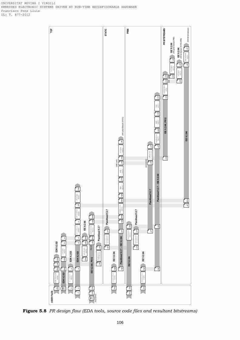
106
Figure 5.8 PR design flow (EDA tools, source code files and resultant bitstreams)
(bus
mac
ros)
.xmp
.xmp
BS
B-w
izard
(ED
K)
BS
B-w
izard
(ED
K)
.ucf
.ucf
.mss
.mss
.mhs
.mhs
EDK
libra
ryED
K lib
rary
.mss
.mss
.mhs
.mhs
libgen
(XP
S)
libgen
(XP
S)
.a.a.h.h
.s.s.a.a
as-
asse
mbl
er
(GN
U)
as-
asse
mbl
er
(GN
U)
.h.h.c.c
.a.a.h.h
.a.a.o.o
gcc
-com
pile
r
(GN
U)
gcc
-com
pile
r
(GN
U)
ld-lin
ker
(GN
U)
ld-lin
ker
(GN
U)
objc
opy
(GN
U)
objc
opy
(GN
U)
.elf
.elf
.hex
.hex
.mhs
.mhs
pla
tgen
(XS
T)
pla
tgen
(XS
T)
.bmm
.bmm
.vhd
.vhd
.vhd
.vhd
.nmc
.nmc
.bmm
.bmm
.vhd
.vhd
synth
esi
s(X
ST
)sy
nth
esi
s(X
ST
).bm
m.bm
m.ng
c.ng
c
.xco
.xco
core
gen
era
tor
(IS
E)
core
gen
era
tor
(IS
E)
.ngc
.ngc
.ucf
.ucf
hdbuild
(Pla
nA
head
)hdbuild
(Pla
nA
head
).uc
f.uc
f
.bmm
.bmm
.ngc
.ngc
ngdbuild
(XS
T)
ngdbuild
(XS
T)
.ngd
.ngd
.bmm
.bmm
.ngc
.ngc
.ucf
.ucf
MA
P(X
ST
)M
AP
(XS
T)
PA
R(X
ST
)P
AR
(XS
T)
.ncd
.ncd
.ncd
.ncd
bitg
en
(XS
T)
bitg
en
(XS
T)
.bit
.bit
.nmc
.nmc
.vhd
.vhd
.ngc
.ngc
synth
esi
s(X
ST
)sy
nth
esi
s(X
ST
)
.xco
.xco
core
gen
era
tor
(IS
E)
core
gen
era
tor
(IS
E)
.ngc
.ngc
.ucf
.ucf
hdbuild
(Pla
nA
head
)hdbuild
(Pla
nA
head
).uc
f.uc
f
.ngc
.ngc
.ngc
.ngc
ngdbuild
(XS
T)
ngdbuild
(XS
T)
.ngd
.ngd
MA
P(X
ST
)M
AP
(XS
T)
PA
R(X
ST
)P
AR
(XS
T)
.ncd
.ncd
.ncd
.ncd
bitg
en
(XS
T)
bitg
en
(XS
T)
.bit
.bit
bitg
en
(XS
T)
bitg
en
(XS
T)
.bit
.bit
.ncd
.ncd
.bmm
.bmm
.elf
.elf
data
2m
em
(XS
T)
data
2m
em
(XS
T)
.bit
.bit
.bit
.bit
EDK 9.2.02i
EDK 9.2.02i
EDK 9.2.02i
EDK 9.2.02i
ISE 9.2.04i
ISE 9.2.04i
ISE 9.2.04i_PR12
PlanAhead9.2.7
PlanAhead9.2.7
–ISE 9.2.04i
I SE 9.2.04i
ISE 9.2.04i
PlanAhead9.2.7
PlanAhead9.2.7
–ISE 9.2.04i
.ucf
.ucf
.ucf
.ucf
(sta
tic.u
sed)
(arc
s.ex
clud
e)
(top.
ucf)
.ucf
.ucf
floor
pla
nne
r(P
lan
Ahe
ad)
floor
pla
nne
r(P
lan
Ahe
ad)
.ucf
.ucf
PlanAhead9.2.7
.ucf
.ucf
floor
pla
nne
r(P
lan
Ahe
ad)
floor
pla
nne
r(P
lan
Ahe
ad)
PlanAhead9.2.7
.ucf
.ucf
.ucf
.ucf
.ncd
.ncd
ISE 9.2.04i
(HW
par
tialb
itstre
amPR
M)
(HW
full
bits
tream
STAT
IC+P
RM
)
(HW
+SW
full
bits
tream
)
(HW
par
tialb
itstre
amST
ATIC
)
.ncd
.ncd
merg
edes
(PR
)m
erg
edes
(PR
).nc
d.nc
d.nc
d.nc
dISE 9.2.04i_PR12
ISE 9.2.04i
(par
tial)
.ncd
.ncd
(full)
ISE 9.2.04i
USER FILES
TOP
STATIC
PRMi
PR BITSTREAMS
PR
libra
ryPR
lib
rary
UNIVERSITAT ROVIRA I VIRGILI EMBEDDED ELECTRONIC SYSTEMS DRIVEN BY RUN-TIME RECONFIGURABLE HARDWARE Francisco Fons Lluís DL: T. 877-2012
107
A. Performance evaluation
The proof of feasibility of the reconfiguration engine has been conducted in a Xilinx ML401 development platform composed of a XC4VLX25 Virtex-4 FPGA from Xilinx and two 256-Mbit HYB25D256160BT-7 DDR-SDRAM devices from Infineon. The system has been mainly described in VHDL and synthesized, mapped, placed and routed with the Xilinx toolset from the Early Access Partial Reconfiguration lounge based on a modular design methodology (http://www.xilinx.com/support/prealounge/protected/index.htm). The processor system has been implemented with EDK 9.2.02i. The floorplanning of all the modules has been performed with PlanAhead 9.2.7. The generation of the full and partial bitstreams has been carried out with ISE 9.2.04i and the PR patch PR12. In addition, the design of specific hard macros has been done with the Xilinx Core Generator toolset, for instance the FIFOs, built with the FIFO Generator v3.3 tool. This tool enables the customization of both depth and width of the FIFO and the selection of distributed memory or embedded RAM blocks. Besides, the ChipScope Pro tool has been used for debugging, validation and verification of the design. This tool has been of big help to test the real latency and performance of the reconfiguration controller. By inserting a ChipScope ICON (integrated controller) core and a ChipScope ILA (integrated logic analyser) core in the design it has been possible to verify the real performance of the reconfiguration controller by monitoring the lines of the ICAP and the NPI buses during the operation. Figure 5.8 shows the PR methodology and design flow followed. The main goal of our approach is to ensure the maximum reconfiguration throughput. As presented above, Virtex-4 technology admits a reconfiguration bandwidth of 3.2 Gbps when running the ICAP controller at 32 bits and 100 MHz. Several scenarios have been evaluated: the first test consists in performing a reconfiguration of the PRR guided by the master MMU while the host processor is not accessing the DDR-SDRAM, just to see which throughput can be achieved in these conditions. The second case evaluates the worst case by forcing the continuous access to DDR-SDRAM from the host processor while the master MMU is reconfiguring a PRR. The results are detailed next. Case I. Shared memory accessed by MMU only (no data contention)
It is programmed an application where the host processor starts a reconfiguration of the PRR and keeps in a waiting loop until the master MMU confirms the end of the bitstream transaction from the external memory to the ICAP. It is necessary to ensure that the code related to the active waiting is executed from the DCACHE, without requiring the CPU to access the DDR-SDRAM. In these conditions, it is observed that once the reconfiguration FIFO is not empty it starts the transfer to the ICAP without suffering any interruption due to lack of data in the FIFO during all the process. The bistream download is conducted through consecutive bursts of 64 words of 32 bits. The equation (5.9) is next particularized to the specific case as follows:
[ ][ ]
[ ][ ]
[ ]bitsN
MHzf
MHzf
bitsw
bitsw
CFG
MMU
CFG
MMU
20483264
100
100
32
64
=⋅=====
CFGCFGMMUMMU
MMU fwfNwL
wN ⋅≥⋅+⋅
⋅
[ ]MMUMMUCFGCFG
MMU clocksw
N
fw
fNL 32
64
2048
10032
1002048 =−⋅
⋅=−⋅
⋅≤
UNIVERSITAT ROVIRA I VIRGILI EMBEDDED ELECTRONIC SYSTEMS DRIVEN BY RUN-TIME RECONFIGURABLE HARDWARE Francisco Fons Lluís DL: T. 877-2012
108
It means that, in these conditions, the latency of each read burst shall be less than or equal to 32 clocks to guarantee the minimum reconfiguration time. The latency L obtained experimentally is 24 clocks for each 64-word read burst performed, measured with the support of the Chipscope ILA logic analyser core. Therefore, starting at the instant that the FIFO receives the first data, the transfer is performed at 3.2 Gbps. The latency achieved experimentally can also be analysed theoretically by examining the interface between the FPGA and the DDR-SDRAM as well as the technical features of this memory. The external DDR-SDRAM is constituted by two 256-Mbit HYB25D256160BT-7 DDR-SDRAM devices [Xilinx Inc., UG080 2006]. Each device is organized in a 16-bit data bus and they are connected in parallel, with the same addressing, in order to reach thus a data bus of 32 bits. Internally, read and write accesses to this DDR-SDRAM are burst oriented, with the burst length being programmable. The burst length determines the maximum number of column locations that can be accessed for a given read or write command. Burst lengths of 2, 4 or 8 locations are available. Therefore, accesses start at a selected location and continue for the programmed number of locations in a sequence. Furthermore, this memory has a read latency of 2.5 clocks and its dual data rate characteristic permit to read or write at both rising and falling edges of the memory clock [Infinieon Tech., DS HYB25D256 2003]. Wih these features, each 64-word (32-bit) NPI read burst commanded by the master MMU is decomposed in 8 consecutive 8-word (32-bit) read bursts in the DDR-SDRAM. In one clock, the two 32-bit words read by the DDR-SDRAM (one at each edge) compose one 64-bit word that can be stored in the 64-bit read FIFO of the NPI interface. Only from the 8 DDR-SDRAM bursts it is obtained a read latency related to the memory itself of 20 clocks (8 x 2.5) and the other 4 clocks are spent in the arbitration and the NPI protocol. Therefore, the total time measured in a NPI read burst, according to equation (5.7), is:
[ ][ ]
[ ][ ]MMU
MMU
MMU
clocksL
bitsN
MHzf
bitsw
24
2048
100
64
==
==
[ ]nsTw
NLT MMU
MMUburst 56010
64
204824 =⋅
+=⋅
+=
Case II. Shared memory accessed by MMU and CPU with data contention
The reconfiguration test of case I has been repeated now but making the CPU to continuously write or read the DDR-SDRAM memory while the master MMU is carrying out the reconfiguration, aimed at seeing how much the reconfiguration process can be slowed due to the collisions. In this case, the latency L observed amounts to 40 clocks, measured with the Chipscope ILA logic analyser core. This 64-word read burst latency is detached in 20 clocks due to memory latency itself as in case I and other 20 clocks due to the arbitration of the collisioned requests between the reconfiguration controller and the host processor to access the shared memory. This latency higher than 32 clocks means that in these conditions it is not possible to perform the reconfiguration at the maximum rate of Virtex-4. However, this extreme situation can be skipped through the use of the cache memory by the CPU. In order to avoid the loss of performance observed in this test, it is convenient to cache the program code executed by the host processor when a reconfiguration is in progress in order to not impact on the reconfiguration latency. If the software host processor is cached, then it is possible to eradicate the additional latency due to the arbitration of the memory resource since the CPU will run the program code from the ICACHE instead of DDR-SDRAM. With this, the DDR-SDRAM is leaved to the master MMU and only from time to time the CPU will access to DDR-
UNIVERSITAT ROVIRA I VIRGILI EMBEDDED ELECTRONIC SYSTEMS DRIVEN BY RUN-TIME RECONFIGURABLE HARDWARE Francisco Fons Lluís DL: T. 877-2012
109
SDRAM to perform some data update. By caching the CPU data and program code, the probability of collision in the access to the shared external memory by the CPU and the master MMU is notoriously reduced. In this way, this architecture lets execute the two tasks, partial reconfiguration and software execution, in parallel without impacting the DDR-SDRAM. Another possibility to improve the efficiency could be the use of a DDR-SDRAM with lower read latency. Anyhow, as conclusion, this reconfiguration engine architecture achieves to transfer the partial bitstream at the maximum throughput of Virtex-4 technology, even if the DDR-SDRAM is accessed by the CPU via XCL or PLBv46 buses at the same time given that, in the end, the CPU runs the program flow in internal BRAM cache, freeing thus the access to the external DDR-SDRAM to the reconfiguration controller. To the best of the author’s knowledge, at the time of finishing the implementation of this reconfiguration controller, around the beginning of 2009, this was the first work to achieve a controller able to self-reconfigure any PR region of the FPGA at the maximum throughput specified by Xilinx technology, overcoming the time performance achieved by other works published until then in the scientist literature by the research community. This design lets attain a bandwidth of 3.2 Gbps with no restrictions on the partial bitstreams size, and residing the downloadable bitstream files stored in external low-cost SDRAM where, moreover, this memory works as a shared resource in the system, i.e. accessible at any time not only by the reconfiguration controller but by any other processor (CPU) connected to the multiprocessor bus. As remark, the designed reconfiguration controller is not using the readback capability, that is, it does not make use of the read port available in the ICAP. However, in case it was necessary, it could be included in the design with no major changes. Finally, the reconfiguration controller modeled and validated in this work is submitted next to benchmarking of other relevant works found in the literature.
5.3.4 Comparison with state-of-the-art architectures
Virtex-4 devices, together with their successors Virtex-5, Virtex-6 and Virtex-7, are at present the state-of-the-art on the subject of commercially available high-performance dynamic partial self-reconfiguration technology. Virtex-4 FPGAs meant a serious advance regarding reconfiguration bandwidth: it comes with a 32-bit data bus ICAP interface qualified to self-reconfigure at run-time any portion of the device at a frequency of 100 MHz, what puts the reconfiguration rate to 3.2 Gbps – the highest bandwidth today in the market. As benchmark, the reconfiguration model proposed in this chapter and prototyped in Virtex-4 is compared next with the latest works found in the scientist literature also based on Virtex-4 technology. As introduction, the Xilinx FPGA vendor made some ICAP controller proposals to be connected to the OPB or PLBv46 buses like OPB HWICAP [Xilinx Inc., DS280 2004] and XPS HWICAP [Xilinx Inc., DS586 2010], respectively. However, in both cases the bitstream transfer from the repository to the ICAP interface is performed by the system CPU, fact that limits the reconfiguration throughput. In the XPS HWICAP controller, for instance, the CPU bursts the required bitstream data directly from main memory. Incoming data is stored within a write FIFO in the reconfiguration controller, from where it can be fed to the ICAP. The XPS HWICAP also provides for read back of configuration resource states. In this case, the frames are read back into the read FIFO one at a time and the CPU reads the data frame directly from there. Experiments with these controllers found in the literature reveal a low reconfiguration throughput. Going on with further examples, the work presented in [Hübner et al., RAW 2010] targets a cost-effective implementation of the reconfiguration controller in terms of resources consumed, leaving in a second term the reconfiguration throughput. Taking into account such goal, the host processor is responsible for performing the bitstream transfer from external memory connected to the ICAP interface. The host processor is connected to the external repository through a MPMC via XCL or PLB buses to internal registers of the core processor and from here to the ICAP interface through a Fast Simplex Link (FSL)
UNIVERSITAT ROVIRA I VIRGILI EMBEDDED ELECTRONIC SYSTEMS DRIVEN BY RUN-TIME RECONFIGURABLE HARDWARE Francisco Fons Lluís DL: T. 877-2012
110
managed by the core processor. The main disadvantage of this architecture is the fact that the core processor is totally blocked during the the reconfiguration process since it performs the bitstream transfer. The throughput reached is 226 Mbps. In [Claus et al., FPL 2008], it is proposed a CoreConnect PLB ICAP controller with DMA capability via PLB bus to accesss the repository and fetch a bitstream through burst transfers, and without involving the CPU, thus off-loading it. The throughput achieved is 2.36 Gbps. In the work [Liu et al., FPL 2009], it is proposed a reconfiguration controller connected to the PLB bus where the partial bitstream is stored in internal RAM blocks of the FPGA, with the subsequent restriction of this solution to small bitstreams of 64 Kbytes as maximum. The highest reconfiguration speed attainable with this solution is 2.97 Gbps. Another approach is deployed in [Manet et al., JES 2008]. This time the ICAP-based reconfiguration controller is based on the CoreConnect OPB bus architecture. The custom controller is equipped with DMA capability and reaches a reconfiguration throughput of 3.0 Gbps. The work presented in [Nabina and Nuñez-Yañez, FPL 2010] develops a system based on the AMBA multiprocessor bus, where the main processor –LEON3 soft-core– and the memory controller are connected to the AMBA AHB bus together with the ICAP controller. As novelty, the reconfiguration controller proposed incudes –in addition to DMA, burst transfers and end transaction notification via interrupt to the host processor– a bitstream decompressor in the datapath. In this way, as the bitstream is stored compressed in the repository, the latency experimented in the transfer from the off-chip memory repository to an internal FIFO buffer present in the reconfiguration controller is decreased since the number of accesses to memory is reduced in comparison to the case of storing the same bitstream uncompressed. The system is implemented in a Virtex-5 device. The low bus efficienty of this system is compensated by the high compression ratio of the bitstream, obtaining a maximum throughput of 3.08 Gbps. This bitstream compression strategy, however, is only effective in case the reconfiguration bottleneck is in the access to the off-chip memory since the bitstream must be transferred uncompressed to the FPGA configuration memory. Another approach which incorpores the bitstream decompression phase in the reconfiguration datapath to improve the transfer rate of the bitstream from the external memory (SRAM) to the reconfiguration controller is [Liu et al., MSR-TR-2009-150]. In this system architecture proposed by Microsoft Research, the decompression operation involves a two-cycle overhead that makes not possible to achieve the theoretical maximum throughput. The tests conducted show a throughput that ranges from 2.99 to 3.14 Gbps. Following a different research line, one approach that makes use of ICAP overclocking is presented in [Shelburne et al., FPL 2008]. The reconfiguration controller is implemented in a Virtex-4 device and admits two types of operations: readback and configuration. Here, the configuration engine is used as a NoC without requiring routing the nodes but communicating them by means of the reconfiguration controller, moving data from one internal RAM block (BRAM) to another through the reconfiguration. That is, the configuration information of the BRAM connected to a node of the network is read by the reconfiguration controller and written to another BRAM related to another node afterwards. In this approach, in order to accelerate the reconfiguration process, the ICAP interface is overclocked at a frequency of 144 MHz and is capable of providing a reconfiguration throughput of 1.75 Gbps. Up to now, none of the implementations assessed have reached the theoretical maximum reconfiguration speed of Virtex-4 technology. The following ones met this target and even overpass it by means of overclocking strategies. In [Delorme et al., ReConFig 2009], it is proposed a reconfiguration controller based on three components: an external SRAM memory exclusively dedicated to store the partial bitstreams, a custom custom reconfiguration controller with access to the ICAP interface, and a MicroBlaze processor interfaced via the CoreConnect OPB bus to the reconfiguration controller through several configuration registers. The reconfiguration controller, after receiving the configuration commands from MicroBlaze, performs the reconfiguration process autonomously. With this architecture, it is achieved the maximum reconfiguration throughput in Virtex-4
UNIVERSITAT ROVIRA I VIRGILI EMBEDDED ELECTRONIC SYSTEMS DRIVEN BY RUN-TIME RECONFIGURABLE HARDWARE Francisco Fons Lluís DL: T. 877-2012
111
running at 100 MHz and 32 bits. Besides, the same reconfiguration approach is tested on a Virtex-5 overclocking the ICAP interface at 125 MHz, reaching a throughput of 4 Gbps. Although this model reaches an excellent reconfiguration performance in terms of time, concerning cost the fact that the reconfiguration controller is based on a dedicated external SRAM memory to store the bitstreams accessible only by the reconfiguration controller –not by MicroBlaze– could mean some handicap to certain types of applications. The exclusive use of this FPGA for storing only bitstreams can be an expensive solution if the application requires other external memory devices for storing application data. Just for this reason, the model proposed in this dissertation makes use of a generic low-cost external memory where any kind of data (program code, application data, partial bitstreams) can be stored and accessed by any of the controllers present in the system. Going on with more examples, the work presented in [Hoffman and Pattichis, IJRC 2011] copes with the implementation of an ICAP-based reconfiguration engine which introduces the use of overclocking with active feedback. During overclocking, it receives active feedback from the System Monitor IP [Xilinx Inc., UG192 2011] to ensure that the device voltage and temperature are within nominal operating conditions. The custom reconfiguration controller leads to a bandwidth of 3.4 Gbps for both reads and writes to the ICAP port. A similar reconfiguration engine approach to the one proposed in this dissertation is the one proposed in [Claus et al., ARC 2010] and [Claus et al., XCell 2010] oriented to a video-based driver assistance system. The PR region lodges different image processing coprocessors multiplexed in time. These hardware accelerators are attached as bus masters to the PLB bus. Thus, the PR region is connected to the system through the PLB interface by means of two separate read and write data buses, each 64-bit wide. With this, the reconfigurable coprocessors can perform direct memory accesses without involving the host CPU. The reconfiguration controller is connected to external DDR-SRAM by means of a MPMC and linked to a NPI bus. It also uses an intermediate FIFO for data buffering. This FIFO permits to split the bitstream datapath in two clock domains, one for the external memory and the other for the ICAP. The ICAP controller can initiate data transactions using DMA and burst transfers. By means of overclocking the ICAP interface, it is obtained a high reconfiguration throughput. Furthermore, the reconfiguration controller includes an online verification module to ensure the reconfiguration is performed correctly in overclocking conditions. The verification consists in a CRC IP module connected between the FIFO output port and the ICAP port to check the data fed into the ICAP. Like this, while the bitstream is pushed into the ICAP, the system calculates in parallel a cyclic redundancy check to ensure the bitstream integrity. If the bitstream was corrupted during the transfer it would be detected by this module and the configuration could be stopped. The reconfiguration throughput reached in a Virtex-4 device at 140 MHz is 4.48 Gbps and a Virtex-5 device at 300 MHz is 9.6 Gbps. Still in the field of ICAP overclocking, in [Hansen et al., IPDPS 2011] it is proposed the design –built with the Xilinx FPGA Editor tool– of an enhanced extension of the Xilinx native ICAP primitive. By extending the ICAP with custom logic it is designed an enhanced ICAP hard macro provided with 64-bit input and output ports. Its function is to widen the data path size of the original ICAP primitive from 32 bits to 64 bits in order to gain configuration throughput. Thus, the enhanced ICAP hard macro can be seen as a 64-to-32 bit data multiplexer that takes 64-bit input data at one data rate and multiplex it out as two 32-bit output data at twice the data rate. This concept is similar to the one proposed by the author in this dissertation by means of the FIFO managed by the master MMU of Figure 5.7. The main progress of this work is that it has explored the limit sustainable by the ICAP, verifying that it is possible to overclock the ICAP interface at up to 550 MHz without malfunction, achieving thus a maximum reconfiguration speed of 17.6 Gbps, a value 5.5 times higher than the default reconfiguration throughput specified by Xilinx. However, the main drawback of this reconfiguration engine is the fact that it does not solve the paradigm related to the data path connection between the bitstream repository and the ICAP interface: the enhanced ICAP hard macro makes use of 64 Kbytes FIFO for temporary storing the partial
UNIVERSITAT ROVIRA I VIRGILI EMBEDDED ELECTRONIC SYSTEMS DRIVEN BY RUN-TIME RECONFIGURABLE HARDWARE Francisco Fons Lluís DL: T. 877-2012
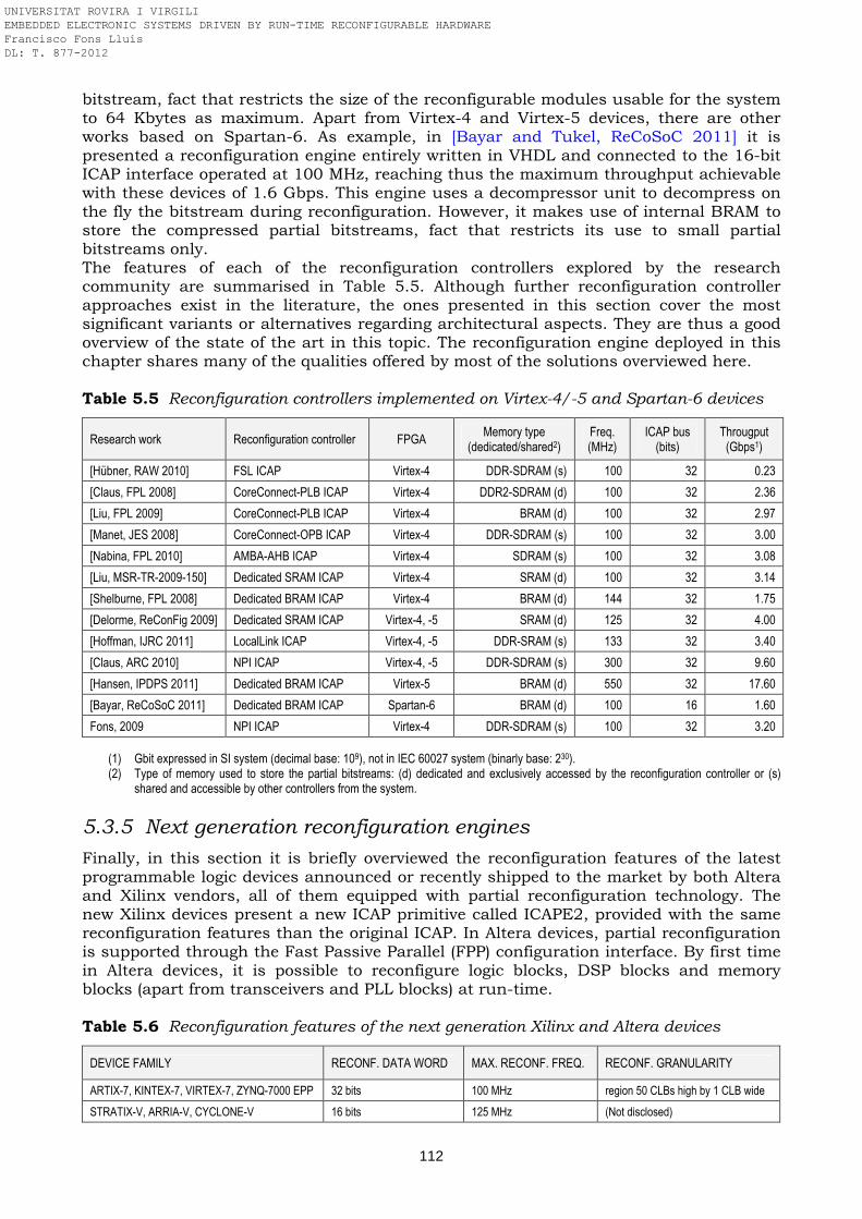
112
bitstream, fact that restricts the size of the reconfigurable modules usable for the system to 64 Kbytes as maximum. Apart from Virtex-4 and Virtex-5 devices, there are other works based on Spartan-6. As example, in [Bayar and Tukel, ReCoSoC 2011] it is presented a reconfiguration engine entirely written in VHDL and connected to the 16-bit ICAP interface operated at 100 MHz, reaching thus the maximum throughput achievable with these devices of 1.6 Gbps. This engine uses a decompressor unit to decompress on the fly the bitstream during reconfiguration. However, it makes use of internal BRAM to store the compressed partial bitstreams, fact that restricts its use to small partial bitstreams only. The features of each of the reconfiguration controllers explored by the research community are summarised in Table 5.5. Although further reconfiguration controller approaches exist in the literature, the ones presented in this section cover the most significant variants or alternatives regarding architectural aspects. They are thus a good overview of the state of the art in this topic. The reconfiguration engine deployed in this chapter shares many of the qualities offered by most of the solutions overviewed here. Table 5.5 Reconfiguration controllers implemented on Virtex-4/-5 and Spartan-6 devices
Research work Reconfiguration controller FPGA Memory type
(dedicated/shared2) Freq. (MHz)
ICAP bus (bits)
Througput (Gbps1)
[Hübner, RAW 2010] FSL ICAP Virtex-4 DDR-SDRAM (s) 100 32 0.23
[Claus, FPL 2008] CoreConnect-PLB ICAP Virtex-4 DDR2-SDRAM (d) 100 32 2.36
[Liu, FPL 2009] CoreConnect-PLB ICAP Virtex-4 BRAM (d) 100 32 2.97
[Manet, JES 2008] CoreConnect-OPB ICAP Virtex-4 DDR-SDRAM (s) 100 32 3.00
[Nabina, FPL 2010] AMBA-AHB ICAP Virtex-4 SDRAM (s) 100 32 3.08
[Liu, MSR-TR-2009-150] Dedicated SRAM ICAP Virtex-4 SRAM (d) 100 32 3.14
[Shelburne, FPL 2008] Dedicated BRAM ICAP Virtex-4 BRAM (d) 144 32 1.75
[Delorme, ReConFig 2009] Dedicated SRAM ICAP Virtex-4, -5 SRAM (d) 125 32 4.00
[Hoffman, IJRC 2011] LocalLink ICAP Virtex-4, -5 DDR-SRAM (s) 133 32 3.40
[Claus, ARC 2010] NPI ICAP Virtex-4, -5 DDR-SDRAM (s) 300 32 9.60
[Hansen, IPDPS 2011] Dedicated BRAM ICAP Virtex-5 BRAM (d) 550 32 17.60
[Bayar, ReCoSoC 2011] Dedicated BRAM ICAP Spartan-6 BRAM (d) 100 16 1.60
Fons, 2009 NPI ICAP Virtex-4 DDR-SDRAM (s) 100 32 3.20
(1) Gbit expressed in SI system (decimal base: 109), not in IEC 60027 system (binarly base: 230). (2) Type of memory used to store the partial bitstreams: (d) dedicated and exclusively accessed by the reconfiguration controller or (s)
shared and accessible by other controllers from the system.
5.3.5 Next generation reconfiguration engines
Finally, in this section it is briefly overviewed the reconfiguration features of the latest programmable logic devices announced or recently shipped to the market by both Altera and Xilinx vendors, all of them equipped with partial reconfiguration technology. The new Xilinx devices present a new ICAP primitive called ICAPE2, provided with the same reconfiguration features than the original ICAP. In Altera devices, partial reconfiguration is supported through the Fast Passive Parallel (FPP) configuration interface. By first time in Altera devices, it is possible to reconfigure logic blocks, DSP blocks and memory blocks (apart from transceivers and PLL blocks) at run-time. Table 5.6 Reconfiguration features of the next generation Xilinx and Altera devices
DEVICE FAMILY RECONF. DATA WORD MAX. RECONF. FREQ. RECONF. GRANULARITY
ARTIX-7, KINTEX-7, VIRTEX-7, ZYNQ-7000 EPP 32 bits 100 MHz region 50 CLBs high by 1 CLB wide
STRATIX-V, ARRIA-V, CYCLONE-V 16 bits 125 MHz (Not disclosed)
UNIVERSITAT ROVIRA I VIRGILI EMBEDDED ELECTRONIC SYSTEMS DRIVEN BY RUN-TIME RECONFIGURABLE HARDWARE Francisco Fons Lluís DL: T. 877-2012
113
5.4 Summary
Going on with the conception of a standard embedded system architecture driven by run-time reconfigurable hardware started in chapter 4, this chapter focuses its attention in the design of the reconfiguration engine. Aimed at minimizing the reconfiguration latency by achieving a high bandwidth link between the bitstream repository and the FPGA configuration memory, the design of this system component is an active research field which has attracted great attention. Hence, this chapter reviews first the technical features of the reconfiguration controllers embedded in commercial devices like Atmel AT94K FPSLIC, Altera Excalibur SoPC and Xilinx Virtex-4 FPGA. Although the first two SoCs offer only a closed engine solution, the third one allows the designer to customize the reconfiguration controller to the application needs. Thus, afterwards, a reconfiguration engine has been modelled and verified on Virtex-4. To the best of the author’s knowledge, this work is a pioneer in terms of achieving the maximum reconfiguration throughput specified by Virtex-4 technology (i.e. 3.2 Gbps – the highest rate of existing devices in the industry today) with no constraints on the partial bitstream size, and being the downloadable bitstream file stored in an external SDRAM memory architected as a shared resource in the system (i.e. not dedicated) accessible concurrently by several processors. Finally, in the part IV of this dissertation, the three reconfiguration engines from different FPGA vendors studied in this chapter have been deeply evaluated by prototyping them in several real applications and verifying the validity of the reconfiguration engine model developed.
References
[Altera Corp., AN116 2000] Altera Corp., Configuring APEX 20K, FLEX 10K, & FLEX 6000 Devices, App. Note 116 (v1.03), 2000.
[Altera Corp., AN187 2003] Altera Corp., Booting Excalibur Devices, Application Note 187 (v1.2), 2003.
[Altera Corp., AN298 2003] Altera Corp., Reconfiguring Excalibur devices under processor control, Application Note 298 (v1.0), 2003.
[Altera Corp., DSAPEX20K 2003] Altera Corp., APEX 20K programmable logic device family, Data Sheet (v5.1), 2004.
[Altera Corp., HRMEPXA 2002] Altera Corp., Excalibur devices hardware reference manual, Reference Manual (v3.1), 2002.
[Atmel Corp., AN1009 2002] Atmel Corp., AT40K series configuration, Application Note 1009, 2002.
[Atmel Corp., AN1088 1998] Atmel Corp., AT40K series Cache Logic (mode 4) configuration, Application Note 1088, 1998.
[Atmel Corp., AN2313 2001] Atmel Corp., AT94K series configuration, Application Note 2313, 2001.
[Atmel Corp., AN2323 2001] Atmel Corp., AT94K series Cache Logic (mode 4) configuration, Application Note 2323, 2001.
[Atmel Corp., RM1138 2008] Atmel Corp., AT94KAL Series Field Programmable System Level Integrated Circuit, Ref. Man. 1138, 2008.
[Bayar and Tukel, ReCoSoC 2011] S. Bayar, M. Tukel, A self-reconfigurable platform for general purpose image processing systems on low-cost Spartan-6 FPGAs, Proc. Int. Workshop on Reconf. Communication-centric SoC, pp. 1-9, 2011.
[Bayar and Yurdakul, HiPEAC 2008] S. Bayar, A. Yurdakul, Dynamic partial self-reconfiguration on Spartan-III FPGAs via a parallel configuration access port (PCAP), Proc. HiPEAC Workshop on Reconfigurable Computing, pp. 1-10, 2008.
[Bomel et al., ARCS 2009] P. Bomel, J. Crenne, L. Ye, J.P. Diguet, G. Gogniat, Ultra-fast downloading of partial bitstreams through Ethernet, Int. Conf. on Architecture of Computing Systems, LNCS, vol. 5455, pp. 72-83, Springer, 2009.
[Cantó et al., FPL 2009] E. Cantó, M. Fons, M. López, R. Ramos, Acceleration of complex algorithms on a fast reconfigurable embedded system on Spartan-3, Proc. Int. Conf. on Field Prog. Logic & Applications, pp. 429-434, 2009.
[Claus et al., ARC 2010] C. Claus, R. Ahmed, F. Altenried, W. Stechele, Towards rapid dynamic partial reconfiguration in video-based driver assistance systems, International Symposium on Applied Reconfigurable Computing, LNCS, vol. 5992, pp. 55-67, Springer-Verlag, 2010.
UNIVERSITAT ROVIRA I VIRGILI EMBEDDED ELECTRONIC SYSTEMS DRIVEN BY RUN-TIME RECONFIGURABLE HARDWARE Francisco Fons Lluís DL: T. 877-2012
114
[Claus et al., FPL 2008] C. Claus, B. Zhang, W. Stechele, L. Braun, M. Hübner, J. Becker, A multi-platform controller allowing for maximum dynamic partial reconfiguration throughput, Proc. Int. Conf. on Field Programmable Logic and Applications, pp. 535-538, 2008.
[Claus et al., IPDPS 2007] C. Claus, F.H. Müller, J. Zeppenfeld, W. Stechele, A new framework to accelerate Virtex-II Pro dynamic partial self-reconfiguration, Proc. IEEE Int. Parallel & Distributed Processing Symposium, pp. 1-7, 2007.
[Claus et al., XCell 2010] C. Claus, F. Altenried, W. Stechele, Dynamic partial reconfiguration of Xilinx FPGAs lets system adapt on the fly, Xcell Journal, issue 70, pp. 18-23, Xilinx Inc., First Quarter 2010.
[Delorme et al., ReConFig 2009] J. Delorme, A. Nafkha, P. Leray, C. Moy, New OPBHWICAP interface for realtime partial reconfiguration of FPGA, Proc. of the Int. Conference of Reconfigurable Computing and FPGAs, pp. 386-391, 2009.
[Gonzalez et al., MICRO 2007] I. Gonzalez, E. Aguayo, S. Lopez-Buedo, Self-reconfigurable embedded systems on low-cost FPGAs, MICRO, IEEE, pp. 49-57, 2007.
[Hansen et al., IPDPS 2011] S.G. Hansen, D. Koch, J. Torresen, High speed partial run-time reconfiguration using enhanced ICAP hard macro, Proc. of the IEEE Int. Parallel and Distributed Processing Symposium, pp. 174-180, 2011.
[Hoffman and Pattichis, IJRC 2011] J.C. Hoffman, M.S. Pattichis, A high-speed dynamic partial reconfiguration controller using direct memory access through a multiport memory controller and overclocking with active feedback, International Journal of Reconfigurable Computing, vol. 2011, pp. 1-10, 2011.
[Hübner et al., RAW 2010] M. Hübner, D. Göhringer, J. Noguera, J. Becker, Fast dynamic and partial reconfiguration data path with low hardware overhead on Xilinx FPGAs, Proc. Reconfigurable Architectures Workshop, pp. 1-8, 2010.
[Infinieon Tech., DS HYB25D256 2003] Infineon, HYB25D256[400/800/160]B[T/C](L) 256-Mbit DDR SDRAM, Datasheet (v1.1), 2003.
[Liu et al., FPL 2009] M. Liu, W. Kuehn, Z. Lu, A. Jantsch, Run-time partial reconfiguration speed investigation and architectural design space exploration, Proc. Int. Conf. on Field Prog. Logic and App., pp. 498-502, 2009.
[Liu et al., MSR-TR-2009-150] S. Liu, R. Neil Pittman, A. Forin, Minimizing partial reconfiguration overhead with fully streaming DMA engines and intelligent ICAP controller, Microsoft Research, Technical Report MSR-TR-2009-150, pp. 1-33, 2009.
[Manet et al., JES 2008] P. Manet, D. Maufroid, L. Tosi, G. Gailliard, O. Mulertt, M. Di Ciano, J.D. Legat, D. Aulagnier, C. Gamrat, R. Liberati, V. La Barba, P. Cuvelier, B. Rousseau, P. Gelineau, An evaluation of dynamic partial reconfiguration for signal and image processing in professional electronics applications, EURASIP Journal on Embedded Systems, pp.1-11, 2008.
[Möller et al., ReCoSoC 2007] L. Möller, I. Grehs, E. Carvalho, R. Soares, N. Calazans, F. Moraes, A NoC-based infrastructure to enable dynamic self reconfigurable system, Proc. Int. Workshop ReCoSoC, pp. 23-30, 2007.
[Nabina and Nuñez-Yañez, FPL 2010] A. Nabina, J.L. Nuñez-Yañez, Dynamic reconfiguration optimisation with streaming data decompression, Proc. of the Int. Conference on Field-Programmable Logic and Applications, pp. 602-607, 2010.
[Paulsson et al., FPL 2007] K. Paulsson, M. Hübner, G. Auer, M. Dreschmann, L. Chen, J. Becker, Implementation of a virtual internal configuration access port (JCAP) for enabling partial self-reconfiguration on Xilinx Spartan III FPGAs, Proc. of the Int. Conference on Field Programmable Logic and Applications, pp. 351-356, 2007.
[Shelburne et al., FPL 2008] M. Shelburne, C. Patterson, P. Athanas, M. Jones, B. Martin, R. Fong, MetaWire: Using FPGA configuration crcuitry to emulate a network-on-chip, Proc. of the Int. Conf. on Field Programmable Logic and Applications, pp. 257-262, 2008.
[Van der Bok et al., ProRISC 2007] K. van der Bok, R. Chaves, G. Kuzmanov, L. Sousa, A. van Genderen, Dynamic FPGA reconfigurations with run-time region delimitation, Proc. Workshop on Circuits, Syst. & Signal Proc., pp. 201-207, 2007.
[Xilinx Inc., DS280 2004] Xilinx Inc., OPB HWICAP, Datasheet 280 (v1.3), 2004.
[Xilinx Inc., DS586 2010] Xilinx Inc., LogiCORE IP XPS HWICAP, Datasheet 586 (v5.00a), 2010.
[Xilinx Inc., DS643 2008] Xilinx Inc., Multi-Port Memory Controller (MPMC), Datasheet 643 (v4.02.a), 2008.
[Xilinx Inc., UG080 2006] Xilinx Inc., ML401/ML402/ML403 Evaluation Platform, User Guide 80 (v2.5), 2006.
[Xilinx Inc., UG192 2011] Xilinx Inc., Virtex-5 FPGA System Monitor, User Guide 192 (v1.7.1), 2011
UNIVERSITAT ROVIRA I VIRGILI EMBEDDED ELECTRONIC SYSTEMS DRIVEN BY RUN-TIME RECONFIGURABLE HARDWARE Francisco Fons Lluís DL: T. 877-2012

Part IV
Proofs of Concept & Use Cases
UNIVERSITAT ROVIRA I VIRGILI EMBEDDED ELECTRONIC SYSTEMS DRIVEN BY RUN-TIME RECONFIGURABLE HARDWARE Francisco Fons Lluís DL: T. 877-2012

UNIVERSITAT ROVIRA I VIRGILI EMBEDDED ELECTRONIC SYSTEMS DRIVEN BY RUN-TIME RECONFIGURABLE HARDWARE Francisco Fons Lluís DL: T. 877-2012
117
Chapter 6 Exploration and exploitation
From long time ago, the scientific community has been actively involved in the search and exploration of potential killer applications for run-time reconfigurable hardware technology. Reconfigurable computing fits well in many application fields and, in this chapter, application domains that benefit from this technology are pointed out. Its potential has been demonstrated in numerous research works, gaining up to several orders of magnitude in performance/cost benefits compared to other traditional implementation alternatives based on static hardware. A survey of potential applications and successful stories of commercial products based on this technology is presented next. In summary, these examples share a common vision about the importance of reconfigurable computing and some very exciting ideas and directions for future work. After this outlook, the next chapters of the part IV of the dissertation encompass the design of specific solutions based on run-time reconfigurable hardware to solve six particular engineering problems. Through these experimental examples developed, the author aims at extracting a compelling methodology to exploit run-time reconfigurable hardware and give evidences of its proof-of-feasibility. It is an attempt to brigde the gap between the theoretical math of engineering apps and the design issues to make it possible in practice with current FPGA devices. They show how to translate an algorithm to a circuit using techniques which match the advantages of area and time multiplexing.
6.1 Potential applications
The goal of this section is to collect a comprehensive list of current computing and engineering applications which, deployed in reconfigurable hardware technology, can contribute to add value to real solutions in both industrial and academic areas. Software-defined radio, cryptography or high-performance computing are among the system applications beginning to use partial reconfiguration today. Furthermore, because this field is still growing, new fields of application are likely to be developed in the future.
6.1.1 Space applications
Electronic systems specifically designed to carry out space applications under strong operating environments (e.g. telecom, military or avionics) are submitted to aggressive requirements and qualification tests concerning features like low-power consumption, reduced weight and size, electromagnetic compatibility (EMC) and, mainly, immunity and tolerance to single event upset (SEU) due to the exposition of the silicon area to cosmic radiation. The atmosphere contains several types of subatomic energetic particles that whether collide with semiconductor devices can cause them some kind of damage, interfering thus with the normal operation of those electronic components. These particles –basically high-energy protons, neutrons and heavy ions– are the result of the collision of both solar and galactic cosmic rays with the oxygen and nitrogen atoms in the Earth’s atmosphere. The single event upsets are radiation-induced errors in microelectronics circuits caused when these charged particles lose energy by ionising the medium through which they pass, leaving behind a wake of electron-hole pairs. If these charges generated in the silicon substrate in CMOS devices are located near to a transistor can be then collected by its source and drain producing a current pulse which, if it is large enough, can finally change the state of a memory cell or configuration bit from logic 1 to logic 0 and vice versa.
UNIVERSITAT ROVIRA I VIRGILI EMBEDDED ELECTRONIC SYSTEMS DRIVEN BY RUN-TIME RECONFIGURABLE HARDWARE Francisco Fons Lluís DL: T. 877-2012
118
Despite SRAM-based FPGAs are more susceptible to particle-induced SEUs than Flash or anti-fuse FPGAs, they are gaining relevance due to its high potential as on-orbit fully/partially reconfigurable systems [Osterloh et al., AHS 2009]. There exists a clear trend towards re-designing the control electronics of space applications up till now based on mask-programmable or one-time programmable (OTP) silicon platforms, such as ASICs or antifuse-based FPGAs (e.g. Actel FPGAs), by introducing SRAM-based FPGAs (e.g. Xilinx and Atmel FPGAs). The reasons are their higher performance and reconfiguration capabilities, as well as the considerable reduction of development time and costs. Besides, SRAM-based FPGAs provide the flexibility to update processing algorithms as needed during the development cycle and even post–launch by replacing faulty/outdated designs at different stages of a mission. That is, reconfigurability can be used to change the resources where a particular function is implemented, upon the successful detection and diagnosis of a fault affecting the area of the device in which it had been originally placed. It is relevant to note here that space qualification for printed circuit boards (PCB) restricts to only a maximum of three soldering and de-soldering cycles for any given pad, therefore the use of SRAM-based programmable logic devices lets skip these constraints since they can be in-system reconfigured repeatedly, once the device is soldered onto the PCB. An additional reason is that the FPGA vendors have already begun to develop SEU mitigation techniques in order to make their devices usable in space applications: the European Space Agency (ESA) is activelly working with the European provider of FPGAs Atmel, which develops radiation-hardened versions of SRAM-based (rad-hard) FPGA devices admitting also run-time reconfiguration (http://spacefpga.atmel-nantes.fr/spacefpga), and the National Aeronautics and Space Administration (NASA) is working with Xilinx FPGAs. Apart from this, it is expected that future space missions will require measurements from high data rate instruments. Recent internal studies at NASA’s Jet Propulsion Laboratory estimate approximately a transaction of 1–5 Terabytes of raw data (uncompressed) per day. Implementations of on-board processing algorithms to perform lossless data reduction are required to drastically reduce data volumes to within the downlink capabilities of the spacecraft and existing ground stations. Reconfigurable FPGAs can include embedded processors thereby providing a flexible hardware and software co–design architecture to meet the on–board processing challenges of these missions while reducing the critical spacecraft resources of mass and volume of earlier generation flight–qualified single board computers. With satellite lifetimes increased far beyond ten years –much longer than the validity of telecom standards– re-programmability in flight becomes a stringent requirement. If software solutions are not possible, dynamically reconfigurable FPGAs may soon be the only solution. In summary, they offer flexibility for changing requirements, in-system and on-orbit programmability as well as potential recovery of in-flight failures.
6.1.2 Bio-inspired applications
Nature has always inspired humans. As proof of this, reconfigurable technology is allowing the physical implementation of bio-inspired systems, emulating the structure, the behavior and the mechanisms of biological organisms. Natural capabilities such as growth, evolution, learning, healing, self-replication or reasoning can be modelled by hardware systems to reach an approach of what could be called artificial life. From a global viewpoint it can be considered that these basic principles are structured around three main axes: phylogenesis (evolution), ontogenesis (growth, self-replication, self-repair) and epigenesis (learning). These three axes are the key representatives of a new hardware conception paradigm known as bio-inspired hardware and, analogous to nature, the space of bio-inspired hardware system can be partitioned along them: the phylogenesis encompasses all the processes which result in what is usually called natural evolution, i.e., the history of the evolution of the species, the development of living species and populations driven by the pressure exerted by the environment. If one considers the specific case of phylogenetic hardware, one finds the domain of evolvable
UNIVERSITAT ROVIRA I VIRGILI EMBEDDED ELECTRONIC SYSTEMS DRIVEN BY RUN-TIME RECONFIGURABLE HARDWARE Francisco Fons Lluís DL: T. 877-2012
119
hardware. The ontogenesis involves the development of a single individual from its own genetic code, essentially without environmental interactions. The self-replication and self-repair capabilities that can be usually observed in living beings and cellular systems are based on the concept of ontogeny, where a single mother cell gives rise, through multiple divisions, to a multiple cellular organism. Ontogenetic hardware mainly involves hardware implementations of self-replicating and self-repairing cellular systems. Finally, the epigenesis handles the learning through environmental interactions that take place after formation of the individual. It consists in the development of an individual through learning processes influenced by both genetic code (the innate) and environment (the acquired). Epigenetic hardware mainly involves artificial neural network hardware architectures. Therefore, these three organisation principles have provided a longstanding inspiration for solving an extensive list of engineering problems as navigation management in autonomous robots, evolutive artificial neural models in applications where an autonomous system reacts and learn in real-time from the environment, the design of fault-tolerant integrated circuits due the continuous semiconductor technology scaling, or online repairing strategies for electronic systems in hostile environments that may damage the device such as space applications discussed above. Many bio-inspired projects have been carried out in the last years on reconfigurable logic architectures. BioWall is an excellent example of a bio-inspired electronic tissue composed by an array of 5700 Xilinx Spartan FPGAs that replicates biological functions in digital hardware [Tempesti and Teuscher, Xcell 2003]. Other research projects are POEtic, which develops an electronic tissue in the form of an ASIC [Moreno et al., MIXDES 2006], and PERPLEXUS, an project that implements a scalable hardware platform made of custom reconfigurable devices for designing systems able to grow by means of cellular replication, where, by using a small configuration bitstream (describing a single cell), it is possible to generate a complete highly complex organism composed of several cells [Thoma et al., ARCS 2007].
6.1.3 Data security applications
With the continuous and rapid expansion of internet and wireless-based communications across open networks, the value of data as a corporate asset itself is growing and data security becomes a mandatory element required in almost any new system architecture. Applications such as electronic banking, electronic commerce, healthcare practice supported by electronic processes and communication, or virtual private networks (VPNs) require an efficient and cost-effective way to address security over public domains. Security, in the context of information technology, refers basically to properties like: confidentiality or assurance that information is not disclosed to unauthorised individuals; integrity, i.e. ensuring that information retains its original level of accuracy; authentication –recognizing/verifying valid users to allow them access to certain system privileges– and non-repudiation. Consequently, cryptography is the fundamental component for securing such confidential data. The security level provided by cryptographic systems depends on aspects as the mathematical features of the algorithm itself, the way it is implemented (e.g. its power consumption and its prevention of power analysis attacks), the management and length of the keys, etc, and these cryptographic algorithms can impose tremendous processing power demands. Furthermore, the swapping between several encryption algorithms at run-time is a feature highly demanded in many communication systems, therefore the cryptographic implementation must support different algorithms or standards, as well as rapid changes of them being upgradeable in the field since, otherwise, interoperability among different systems is prohibited and any upgrade results in excessive cost. In addition, each security association or link is restricted by its lifetime, after the expiration of which, a new security association has to be established by dynamically negotiating the security parameters between the communicating entities. The ultimate solution for cryptography in terms of flexibility and data transfer rates in line with these demands is an adaptive
UNIVERSITAT ROVIRA I VIRGILI EMBEDDED ELECTRONIC SYSTEMS DRIVEN BY RUN-TIME RECONFIGURABLE HARDWARE Francisco Fons Lluís DL: T. 877-2012
120
cryptographic processor. Just this target is reachable by means of reconfigurable hardware technology. Encryption applications, which involve repetitive computation and have inherent parallelism of large data, are specifically well suited to the use of FPGAs. Reconfigurable hardware emerges as a superior implementation platform with which to address these high-computational algorithms to reach secure applications and overcome the drawbacks of software-based alternatives. Besides, at lowest level, some inherent implementation features of the encryption/decryption algorithm as the change of keys and sub-keys generation, data permutations, data shift, or dynamic changes of constant coefficient multipliers (KCM) and constant coefficient adders (KCA), and the exploitation of hash functions, e.g. Secure Hash Algorithm (SHA), to implement a cryptosystem which can switch between several hash functions are all well-suited to be handled through reconfigurable hardware. Summarizing, reconfigurable hardware devices such as SRAM-based FPGAs combine potential advantages of SW and HW implementations in cryptographic applications. As examples, many works exist which show the benefits of deploying cryptographic systems based on reconfigurable hardware for IDEA and AES algorithms [Gonzalez et al., FPL 2003], [Granado et al., MEJ 2009], aimed at using the hardware resources in an optimal way. Moreover, other viewpoint is presented in [Mentens et al., CHES 2008], where it is exploited the use of dynamic reconfiguration to improve the resistance of cryptographic systems against physical attacks. A new class of countermeasures are introduced which provides increased resistance, in particular against fault attacks, by randomly changing the physical location of functional blocks on the chip area at run-time –introducing in this way spatial jitter by means of random relocation of the functional blocks– and by randomly positioning registers in between functional blocks by means of a dynamically reconfigurable switch matrix to introduce delays – countermeasures that aim at introducing temporal jitter into the sequence of operations in order to desynchronize the observations of power consumption. Therefore, in order to improve the resistance of the implementation against fault analysis attacks, it is proposed a dynamically architecture in which both the location of the subfunctions and the addition of intermediate registers is altered randomly based on a true random number generator to introduce a spatial and temporal jitter.
6.1.4 Thermal self-protected systems
If an integrated circuit is submitted to a severe thermal stress, for instance leading the chip to an increased junction temperature or to the presence of regions that dissipate excessive amounts of heat (hotspots), this overtemperature unleashes negative effects in the device like performance degradation or increase in its leakage current. Hence, the thermal testing/monitoring of an electronic design plays a vital role to ensure safe and reliable thermal operating conditions. In addition to static techniques to remove the heat from the die and reduce the temperature (e.g. sophisticated chip packaging techniques), dynamic techniques of thermal management are essential. Such techniques rely on accurate on-chip temperature information. Thermal monitoring by employing thermal sensors is a widely used technique for assessing thermal behavior of integrated circuits and providing thus preventive measures at run-time to ensure a reliable operation of the device and make it to self-adapt to the environment in case of overtemperature. Traditionally, microprocessors operate only at a single frequency and voltage, thus always consuming full power; however, state-of-the-art microprocessors are built to allow their voltage and frequency to be scaled to decrement power usage before the chip overheats and improve thus the battery life in laptops and handheld devices where they are used (e.g. Intel Xeon processor). Similarly, in the field of programmable logic devices, FPGA circuits can operate at reconfigurable operating frequencies. Besides, their power dissipation depends on the characteristics of the specific application placed and routed in the FPGA. In order to obtain the termograph of either the whole FPGA device or a specific region, an array of on-chip thermal sensors should be distributed along the area
UNIVERSITAT ROVIRA I VIRGILI EMBEDDED ELECTRONIC SYSTEMS DRIVEN BY RUN-TIME RECONFIGURABLE HARDWARE Francisco Fons Lluís DL: T. 877-2012

121
under study. A way to measure chip heating is to construct a ring oscillator and calibrate its output drift in MHz/ºC. A ring oscillator consists of a feedback loop that includes an odd number of inverters needed to produce the phase shifting that maintains the oscillation, with the particularity that the resulting period is twice the sum of the delays of all elements that compose the loop. Ring oscillators are extensively used for implementing thermal sensors on the FPGA fabric since their advantages as thermal transducers are multiple: they can be implemented with few hardware resources (the inverters can be easily synthesized as gates “not” in LUTs of the FPGA) and they can be placed in virtually any position of the chip; moreover, they can be inserted, moved or eliminated by means of dynamic reconfiguration, making possible the construction of a thermal map of the die without requiring any external equipment; also, they do measure the junction temperature and not the package temperature, and unlike reusing specific thermal sensing diodes or I/O pad clamping diodes present in some FPGAs, no I/O pads are necessary to measure the die temperature, hence it is not necessary to make any PCB modification. As application examples, López-Buedo et al. present a thermal monitoring strategy suitable for FPGA-based systems based on the idea that a fully digital temperature transducer can be dynamically inserted, operated, and eliminated from the circuit under test using reconfiguration [López-Buedo et al., TCPT 2002]. Similarly, Jones et al. exploit these ideas on an image processing application implemented on a Xilinx Virtex-4 FPGA [Jones et al., FPL 2007]. By time-multiplexing the system between running the application and making a temperature measurement, they present an adaptive mechanism that automatically adjusts some system operating parameters to yield the best performance for the given environmental conditions, overcoming thus the performance loss in such systems due to overtemperature. The image recognition system sustains a safe operational temperature by automatically adjusting its frequency and output quality to self-regulate its temperature. Like this, the circuit sacrifices output performance and quality to lower its internal temperature as the ambient temperature increases, and can leverage cooler temperatures by increasing output performance and quality. The adaptive application firstly reduces its frequency and secondly the number of cores as well as their size and functional characteristics in order to operate safety under worst-case thermal conditions. In this way, this solution adaptively reacts to changing environmental conditions to obtain the highest possible performance while maintaining a safe temperature. Furthermore, the circuit is able to shutdown if the ambient temperature becomes too hot for the device to function properly; this is performed by downloading a blank bitstream to the FPGA. As summary, thermal monitoring is a valid application field for reconfigurable hardware. The reconfiguration capability of FPGAs transforms these devices into a powerful tool for the study of thermal aspects of ICs and packaging, making possible new alternatives for building thermally self-protected systems.
6.1.5 Software defined radio
In the last years, there has been a strong push to replace analog radio systems by digital radio systems. The Joint Tactical Radio System (JTRS) program of the US Department of Defense shifted the emphasis on the development of software-defined radio (SDR) aimed at doing an essential step towards the unification of radio communication systems, the transparency of services and the exchangeability of components. Like this, SDR is considered a key technology expected to play a decisive role in the wireless communication evolution and spectrum management. It basically refers to a set of techniques that permit the reconfiguration of a communication system without the need to change any hardware system element. The goal is to solve incompatible wireless network issues by implementing radio functionalities as software modules running on generic hardware platforms. The key point is the fact that this adaptation shall be dynamic, in real-time, and even on the fly in case service continuity is required (e.g.
UNIVERSITAT ROVIRA I VIRGILI EMBEDDED ELECTRONIC SYSTEMS DRIVEN BY RUN-TIME RECONFIGURABLE HARDWARE Francisco Fons Lluís DL: T. 877-2012

122
roaming, reconfiguring the terminal to change from one network to another without losing the connection). Although the idea of having a single versatile hand-held device supporting a large number of wireless standards and enabling ubiquitous connectivity through seamless handovers is not new, still today the major bottleneck is the need for low cost, low power consumption, multi-purpose chipsets that support a large variety of bit rates, modulation formats, physical bandwidths and carrier frequencies. Nevertheless, multi-purpose SDR systems turn out to be the only viable option to enable cost-effective mobile terminals incorporating multiple wireless technologies. Only recently, semiconductor technology has evolved to make SDR possible. Although typical architectures implement waveforms in the digital domain using MCUs and DSPs, today the new generation of partially and dynamically reconfigurable FPGAs have specific features which enable SDR implementation. Conceptually, a SDR is a radio communication system which can tune to any frequency band (e.g. GSM, DECT, WLAN) and receive any data modulation (e.g. BPSK, QPSK, OFDM) across a large frequency spectrum by means of programmable hardware controlled by software. Some examples of SDR platforms synthesized in run-time reconfigurable hardware are [Delahaye et al., WSR 2004], where the system is composed of one TI DSP C6201 and one Xilinx FPGA Virtex 1000E driven by run-time partial reconfiguration, and [Rauwerda and Smit, ProRISC 2004], where it is used a coarse-grained reconfigurable MONTIUM processor. Thus, in general, the adaptivity features of the SDR falls into four broad classifications, ordered in an increasing level of both adaptivity and sophistication: functions (e.g. basic building blocks such as Kahlman filters, fast Fourier transforms (FFT) and finite impulse response (FIR) filters), components (e.g. digital down converters and digital up converters which adapt to waveforms that support different bit rates or sampling rates), applications (e.g. modulators) and services (e.g. radio services, network awareness services, ad-hoc networking and even anti-jam services) shall be able to adapt to changing conditions as needed. These levels of adaptivity are possible with PR-FPGAs, although the SDR platforms are still in their early development stages and many issues must be solved to reach the flexibility, scalability and reconfigurability demanded. However, this research field has attracted a large expectation of both industry and academia, and the advances in FPGAs lets be a step closer toward the deployment of reconfigurable radios.
6.1.6 Control applications
There are many application fields which build real-time control systems based on PID, fuzzy logic, artificial neural networks (ANN) or state-space controllers. The need for a transparent and straightforward design methodology of controllers often leads to software implementations, that is, microprocessor programs described in a high-level language using floating-point arithmetic. This approach, however, is inappropriate for some applications that require high sampling rates with short computational times. Like this, FPGA technology exploiting run-time reconfiguration has been explored in the field of control applications, resulting in an efficient alternative to controllers executed by either software-based processors or synthesized in fixed hardware. Many industrial processes, due to their nature, present a dynamic behavior modelled by a set of operating regimes. Each of these regimes is delimited by a series of environment conditions (temperature, humidity, etc) in which the system can be immersed. Thus, depending on the changing environment, the plant must change its operating regime at real-time by adapting its plant controller (either small changes as modifying some parameters of a controller or big structural changes like adding and removing some processing units) to the new operation conditions. With conventional methods it might be possible to design a controller able to control the plant in all operating regimes, but often it is not possible to guarantee optimal working conditions in all the operational range. Parameter adaptive controllers could be used, but they might respond too slowly to abrupt changes of the plant’s dynamic behavior. In this case, it is possible a multiple-model approach
UNIVERSITAT ROVIRA I VIRGILI EMBEDDED ELECTRONIC SYSTEMS DRIVEN BY RUN-TIME RECONFIGURABLE HARDWARE Francisco Fons Lluís DL: T. 877-2012
123
composed of a set of controller modules implemented in static hardware, each optimized for a special operating regime of the plant, with a supervisor module responsible for switching among the controller modules to determine the active module. However, in this multi-controller architecture, although all modules are instantiated in parallel, only one controller module is active at one time, leading to an inefficient design in terms of area and power consumption. Partial run-time reconfiguration can increase the resource efficiency by keeping the currently active controller on the FPGA while inactive controllers are stored in an external NVM. As example, the University of Paderbon proposed an architecture where two controller modules coexist in hardware, one in foreground and the other in background, in order to hide the reconfiguration time typical of the controller switching during normal operation. This architecture takes advantage of the inherent features of the reconfigurable hardware [Danne et al., FPL 2003]. A similar approach exploiting the benefits of partial reconfiguration is found in the work of Rümmele-Werner et al. oriented to the design of a real-time multi-object-tracker. The system is able to track three objects simultaneously by using different algorithms to get the best result. By using the dynamic partial reconfiguration capability of FPGAs, the algorithms can be exchanged during run-time without interrupting the object-tracking process [Rümmele-Werner et al., ISCAS 2011]. Other example of controller that can benefit from run-time reconfigurable hardware technology is the design of artificial neural networks since this technology provides designers with a very flexible platform for the development of adaptive digital circuits. Most types of neural networks have two operation modes which are processed depending on the moment of the execution: training and operation. As the algorithm used in each mode is different, it is possible to switch from one mode to another by implementing the two specific hardware circuits in a reconfigurable FPGA. Moreover, many neural networks training algorithms, in turn, can be partitioned into a series of smaller sub-algorithms that are sequentially executed. This partitioning can be exploited by FPGAs because only one of the sub-algorithms needs to be implemented in hardware at any time. Moreover, some types of neural networks have many different types of training algorithms, and each one of these algorithms would require its own special hardware. This allows a more effective use of hardware resources. All these criteria were put in practice by the Reconfigurable Logic Laboratory at the Brigham Young University (BYU) to develop the so-called Run-Time Reconfiguration Artificial Neural Network (RRANN and RRANN2) as a proof-of-concept system that demonstrates the effectiveness of run-time reconfigurable FPGAs for implementing neural networks [Eldredge and Hutchings, VLSI 1996]. The RRANN architecture, designed on Xilinx XC3090 FPGAs, divides the backpropagation algorithm into the sequential execution of three time-exclusive stages known as feed-forward, backpropagation, and update. This work was extended later in the RRANN2 project, implementing theANN on a fine-grained SRAM-based FPGA with run-time partial reconfiguration –the National Semiconductor CLAy31 FPGA– where the reconfiguration process entails only reconfiguring those portions of the FPGA that change between two consecutive configurations [Hadley and Hutchings, FCCM 1995].
6.1.7 Hardware emulation and rapid prototyping
Today’s embedded systems design has to deal with the growing complexity implied by the combination of emerging technologies and the increasing need for reconfigurability motivated by the combination of the backward compatibility demanded to the current products and the emergence of new protocols/standards or functionality in general. With this, one of the most difficult tasks in the design of modern complex embedded systems is the validation phase. In this sense, the use of FPGA dynamic reconfiguration technology allows having an early analysis of the behavior of the system under almost real conditions while providing an extreme flexibility for embedded validation by adding or modifying the design: different specific peripherals or trace mechanisms can be included on the FPGA on demand to improve the observability and even controllability of
UNIVERSITAT ROVIRA I VIRGILI EMBEDDED ELECTRONIC SYSTEMS DRIVEN BY RUN-TIME RECONFIGURABLE HARDWARE Francisco Fons Lluís DL: T. 877-2012
124
the system. This specific data path to extract information from the device under test can be configured and removed on-the-fly adapted to different test situations. The system can then run during long tests, where different operations are performed and different equipment is connected, without having to stop the whole system. This concept can also be extended to the debug phase, where traditionally there has been a problem of visibility of internal signals. This limited visibility can be overcome by adding reconfigurable monitoring IPs on the fly on the design under test. Such adaptable system design offered by the reconfigurable hardware has been particularly popular among test equipment manufacturers since reconfigurable FPGAs can be used to adapt the same hardware to perform varying types of tests. Moreover, another valuable feature exploited by run-time reconfigurable hardware is the system failure injection [Antoni et al., DFT 2000].
6.1.8 Digital signal processing and arithmetic computing
Many embedded applications implement digital signal processing algorithms to perform certain functionality. In specific domains, software-based implementations do not attain the level of performance required. In such cases, characterized typically by aggressive real-time constraints, hardware coprocessors provided with a high level of parallelism and attached to the host processor are often the solution. Many of these coprocessing architectures, furthermore, demand a level of flexibility and versatility not reachable with static hardware. Run-time reconfigurable hardware technology fits well in such applications oriented to signal filtering, data transmission, arithmetic computing, etc. As examples, in the field of digital filtering, the capability of reconfiguring a filter at run-time is of special interest for applications such as wireless communications or SDR [Delahaye et al., MWCS 2007]. Llamoca et al. developed a 1D FIR filtering system on distributed arithmetic of an FPGA platform that lets, by means of dynamic partial reconfiguration, to reconfigure either only the filter coefficients or the full filter core architecture, modifying the number of coefficients as well as the coefficient values [Llamoca et al., IJRC 2010]. The same concept based on run-time reconfigurable hardware has been successfully applied to the implementation of other use cases like discrete wavelet transform, fast Fourier transform (FFT), discrete cosine transform (DCT), etc. In the area of arithmetic computation, reconfigurable systems achieve significant increases in performance by adapting to computations that are not so well supported by general-purpose processors. Such computational systems are based on processing units customized to the requirements of a particular application. In this context, special attention is given to problems in the area of combinatorial optimization. Among them, the boolean satisfiability (SAT) problem stands out because of the extremely wide range of practical applications in a variety of engineering areas, including the testing of electronic circuits, pattern recognition, logic synthesis, etc. SAT is a very well-known combinatorial problem that consists of determining whether for a given boolean formula, composed of a set of clauses and variables, there exists an assignment of values to the variables which makes the given formula true. Implementations based on reconfigurable hardware enable the primary operations of the respective algorithms to be executed in parallel. Consequently, the effect of exponential growth in the computation time can be delayed, thus allowing larger size instances of SAT to be solved. Recently, several research groups have explored different approaches to solve the SAT problem with the aid of reconfigurable hardware [Skiliarova and De Brito, TOC 2004].
6.1.9 Image processing and multimedia applications
Real-time image processing systems are finding many new applications in areas such as real-time video processing, medical instrumentation or multimedia. Most of these systems are commonly implemented on general-purpose processors; however, an alternative solution is the use of reconfigurable computing systems, which have demonstrated their efficiency to execute complex algorithms satisfying the simultaneous
UNIVERSITAT ROVIRA I VIRGILI EMBEDDED ELECTRONIC SYSTEMS DRIVEN BY RUN-TIME RECONFIGURABLE HARDWARE Francisco Fons Lluís DL: T. 877-2012
125
application needs of performance and flexibility. Moreover, computer vision algorithms are characterized by complex and repetitive operations on large amounts of data involving a variety of data interactions (e.g., point operations but also neighbourhood operations) and they can be efficiently synthesized in dedicated hardware coprocessors. Apart from image processing, in the multimedia and consumer electronics domain, audio processing is also of relevance. The boom of sales of portable multimedia devices in the past years went joined with the appearance in the market of many emerging compression and communication technologies adopted in standards organizations such as ISO, ITU and IEEE. As example, the MPEG and JPEG groups have developed standards to address the compression needs of audio and video. These compression standards address a broad range of application areas, such as digital video broadcast, medical imaging, video surveillance and digital cinema. In this direction, new standards offer unprecedented levels of performance but at a computational cost that favors FPGA technology over traditional processor-based solutions. Besides, the tremendous growth of formats makes dynamic reconfigurable FPGAs an effective platform for this kind of applications to support and play whatever new multimedia format under the same hardware platform. As use case, in [Castillo et al., ReConFig 2006], it is presented a multimedia player system that can be self-reconfigured with appropriate hardware codec to perform the audio and video reproduction depending on the multimedia file to be played, e.g. audio coding formats like WAV (Waveform Audio Format) and MP3 (MPEG-1 Audio Layer 3), or video formats such as JPEG (Joint Photographic Experts Group) and MPEG-2 (Moving Picture Experts Group). Still in the field of multimedia applications, the expansion of wired and wireless network infrastructures and advancement of electronic devices enable the society to enjoy a new life style where we download added-value contents from remote servers and play them on local PCs or embedded appliances such as smart phones. As example, IMEC developed a reconfigurable Internet camera called Cam-E-Leon, combining reconfigurable hardware and embedded software. The appliance implements a secure VPN (Virtual Private Network) with 3DES encryption and an Internet camera server (including JPEG compression), which is run-time reconfigurable by the client, allowing to switch among several available image manipulation functions from a web browser [Desmet et al., SAMOS 2002]. Other work related to video compression is the one performed in [Ramachandran and Srinivasan, VLSID 2002], where a dynamically reconfigurable video encoder lets switch among JPEG, MPEG-1, MPEG-2 and H.263 standards through the partitioning of the algorithm using dynamic reconfiguration. The video encoder is implemented on the Atmel AT6000 FPGA and the dynamic reconfigurability for the entire encoder system is confined to only a portion of a Variable Length Coder (VLC) module residing in the FPGA. This video encoder presents a flexible solution to dynamically switch from one standard to another, changing program features like colour, picture size and channel rate to achieve the desired image quality.
6.1.10 Telecommunications and networking
The recent proliferation of wireless communication systems has highlighted the need to dynamically adapt communications architectures at the hardware level, characterized via a set of configurable parameters. Many other application fields arise in the area of telecom and networking, like data error recovery. The use of error-correcting codes has proven to be an effective way to overcome data corruption in digital communication channels. For this, the system is composed of an encoder and a decoder, separated one from the other by a communication channel exposed to different sources of noise. Encoding is accomplished through the addition of redundant bits into the binary information sequence that is transmitted over the communication channel. These redundant bits provide the decoder with the capability to detect and correct transmission errors originated by the effects of noise and interference into the communication channel. Thus, values received at the decoder may differ from values sent by the encoder due to the noisy and error-prone channel, affected by characteristics such as weather
UNIVERSITAT ROVIRA I VIRGILI EMBEDDED ELECTRONIC SYSTEMS DRIVEN BY RUN-TIME RECONFIGURABLE HARDWARE Francisco Fons Lluís DL: T. 877-2012
126
(wireless communication), distance or battery-power. The changes in these parameters result in a change in the signal-to-noise ratio (SNR). The function of the decoder is to attempt to reconstruct the input sequence transmitted by the encoder by evaluating the received channel output, and the performance of this decoder is characterized by the bit error rate (BER), i.e., the ratio of the number of decoded output bits in error to the total number of bits transmitted. The ability of error correction codes to increase the signal to noise ratio of a communication channel depends on the code chosen. Several of these coding/decoding (CODEC) strategies implemented on reconfigurable hardware are presented next. Viterbi and Adaptive Viterbi decoders are some of the most extensively used
techniques for detecting and correcting error in communication systems based on convolutional codes. Their implementation is typically accomplished by means of shift registers and logic (XOR) functions. As example, Swaminathan et al. proposed the implementation of a dynamically reconfigurable adaptive Viterbi decoder implemented in reconfigurable hardware [Swaminathan et al., FPGA 2002]. In this way, if the channel noise increases, a more accurate but slower running decoder is swapped into the FPGA hardware. Reduced channel noise leads to the opposite effect, downloading in hardware a decoder version of reduced computation and memory to support faster performance and achieve the same decode accuracy.
Turbo codes are other error-correction codes based on redundant data transmission. The component encoder consists of a shift register augmented with generator functions (AND and XOR) to compose one or more parity bits per each input bit. Liang et al. developed a dynamically reconfigurable ASOVA (Adaptive Soft Output Viterbi Architecture) turbo decoder mapped on an Altera Stratix FPGA [Liang et al., FCCM 2004]. Dynamic reconfiguration is used to ensure that, in response to changing channel conditions, the lowest-power decoder that meets the required BER is present in the FPGA at any time, while saving power in comparison to a static implementation.
Reed-Solomon (RS) codes are further examples of codes used to perform Forward Error Correction (FEC) by introducing redundancy in data before they are transmitted. The fundamental operations in RS encoding and decoding involve Galois field arithmetic. These codes are particularly well suited to correct burst errors, in which a continuous sequence of bits is received with errors. Haase et al. developed a Reed-Solomon coder/decoder taking advantage of the partial dynamic reconfiguration of Xilinx Virtex FPGA devices [Haase et al., DATE 2002].
Apart from error correction algorithms, in the field of networked applications, the always increasing demands of the Internet directly affect the requirements of networking routers and firewalls in aspects like data bandwidth and flexibility to support the implementation of new features and functions, e.g. new protocols, enhanced security, all of course without involving prohibitive costs. On the one hand, existing router architectures that provide sufficient flexibility and data-flow processing employ software-based platforms containing multiple RISC cores, therefore some features can be added or removed in the router by upgrading the software in the system. The sequential nature of the microprocessor, however, can limit the system throughput. On the other hand, existing high-performance router architectures capable of data processing at optical line speeds employ ASICs to perform parallel computations in hardware. Nevertheless, these architectures often provide limited flexibility for the deployment of new applications or protocols due to the static nature of the ASIC circuit and consequently they need longer design cycles and higher costs than software-based solutions. In this context, the diversity of networking applications and data flows suggests dynamically reconfigurable hardware to cover this potential design space. As example, the Applied Research Lab from the Washington University developed the Field Programmable Port Extender (FPX), a prototype which enables customized packet processing functions to be implemented as modules which can be dynamically loaded into hardware over a network. Each of these modules, called Dynamic Hardware Plugins (DHP), is deployed in the physical router. The DHP architecture employs reconfigurable hardware to provide a flexible hardware
UNIVERSITAT ROVIRA I VIRGILI EMBEDDED ELECTRONIC SYSTEMS DRIVEN BY RUN-TIME RECONFIGURABLE HARDWARE Francisco Fons Lluís DL: T. 877-2012
127
processing environment for programmable multi-port routers, allowing multiple hardware applications to be dynamically loaded into a single device and run in parallel. The modular design of the FPX makes the system of interest for active networking systems as it allows customized applications to achieve the higher performance via hardware acceleration while these modular components can be dynamically reconfigured over the Internet [Taylor et al., OPENARCH 2001].
6.1.11 Automotive applications
There exist many potential applications in the automotive industry which can take advantage of run-time reconfigurable computing like driver assistance, infotainment (information & entertainment), telematics (the convergence of mobile telecommunications and information processing in vehicles) or the traditional body control and engine management functions. Today, the automobile is provided with novel functionality; linked to this trend, the percentage of vehicle added-value due to mechanical parts is constantly decreasing while the percentage related to electronic components goes just in the opposite direction embedded in the electronic control units (ECUs) present in the vehicle. These ECUs are requested to increase their computational power to join and take charge of much more functionality. In an attempt to manage this complexity, DaimlerChrysler AG in cooperation with the Institute for Information Processing Technology (ITIV) of the University of Karlsruhe investigated the design of an automotive ECU based on the usage of dynamic and partially reconfigurable hardware [Becker et al., IEEE 2007]. Partial and dynamic run-time self-reconfiguration of FPGA devices enables the development of adaptive hardware for a huge variety of applications. In this approach, the typical microcontroller as central component of an ECU is replaced by a dynamically and partially reconfigurable FPGA able to provide vehicle functions on demand. This approach is based on the fact that not all vehicle functions must be available or needed at the same time –in fact, this neither happens today in a vehicle when several functions or tasks are sequentially executed by the same MCU within an ECU– therefore it should be possible to identify an adequate subset of functions which can be operated on the same reconfigurable resource by applying a kind of flexible demand-driven time-multiplexing. This fact makes possible to save hardware resources and power consumption. In the work conducted by Daimler and ITIV, the system consists of a run-time module controller, implemented on a MicroBlaze soft-core processor and four reconfigurable module slots where the different hardware-based application functions are dynamically downloaded and executed on-demand. The system is prototyped in a Xilinx Virtex-II FPGA device. In the static region of the FPGA, a MicroBlaze sof-core processor is the host CPU of the system. The system is connected to its environment via a Controller Area Network (CAN) bus, which is a well established communication interface in the automotive domain. The CPU manages the execution of the different applications or tasks requested via CAN frames in the different reconfigurable regions or partitions of the FPGA. If the task requested via CAN requires a dedicated processor that is not placed at that time in the partially reconfigurable regions, then the reconfiguration controller looks for a free partition and handles the reconfiguration by downloading its bitstream from external Flash memory. This system was implanted in a real car for conducting system tests in a real-world scenario to deploy body functions like seat memory, window lifter or rear mirrors. The results prove that the reduction of power dissipation by adapting the hardware to the actual demand of the application is possible with reconfigurable hardware by means of a dynamically and partially reconfigurable FPGA.
6.1.12 High-performance computing
The potential of FPGAs for scientific computation, high-performance computing or supercomputing is well understood today although their long implementation cycles have
UNIVERSITAT ROVIRA I VIRGILI EMBEDDED ELECTRONIC SYSTEMS DRIVEN BY RUN-TIME RECONFIGURABLE HARDWARE Francisco Fons Lluís DL: T. 877-2012
128
hindered their faster adoption for numerically intensive applications. At present, various key research contributions and initiatives propel FPGA-based computation from the embedded space into scientific computing. A large set of examples can be found in the literature, such as bioinformatics and computational biology, financial computing, astrophysics simulations or weather and climate modelling. Pattern matching, for instance, is an application domain extended in the area of bioinformatics, speech recognition, or in search engines. In many cases, regular expression pattern matching needs to support high processing throughput at lowest possible hardware cost. When performance is critical, software platforms may not be able to provide efficient regular expression implementations. It is a fact that they can be more than one order of magnitude slower than hardware implementations, their performance does not scale well as the number of regular expressions increases and their memory requirements may be substantially large. Parallel hardware architectures offer large advantages in time performance compared to software designs, due to easily extracted parallelism in the intrusion detection string-matching problem. A generic ASIC design would be fast but not suitable due to the dynamic nature of the ruleset –as new vulnerabilities and attacks are identified, new rules must be added to the database and the device configuration must be regenerated. Compared to CPU- or ASIC-based designs, an FPGA allows for exceptional performance due to the parallel hardware nature of execution as well as the ability to customize the device for a particular set of patterns through on-the-fly reconfiguration of a new ruleset. FPGAs can operate at hardware speed and exploit parallelism. Moreover, they provide the required flexibility to change the regular expression ruleset implementation on demand. As the size of the regular expressions set grows, conventional CPU performance may deteriorate appreciably compared to an FPGA-based approach. Consequently, regular expression pattern matching is an application field suitable to best exploit the advantages of reconfigurable hardware.
6.2 Success cases of commercial products and industrial applications
The potentiality of all these applications fields enumerated in the previous section has encouraged the FPGA vendors, supported by research groups in universities, to develop this technology to definitely move it from research to industry. In this sense, additional indicators which confirm the acceptance of run-time reconfigurable hardware is the slow but progressive emergence in the market of commercial products or real use cases that take advantage of this technology in the way of end applications. Nowadays, a very reduced set of commercial products and industrial apps have revealed that make use of run-time reconfigurable hardware technology. These success stories can be probably turned out into the beginning of a new computing wave.
6.2.1 Consumer electronics
Sony Corp. released in 2003 the industry’s first consumer electronics product –the Network Walkman NW-MS70D– driven by run-time hardware reconfiguration technology (so-called Virtual Mobile Engine or VME) for audio codecs. Other commercial products from Sony which integrate run-time reconfigurable hardware are the PlayStation Portable console (PSP) or the Network Walkman NW-E405, deployed through VME technology [Sony Corp., CX-NEWS 2009].
6.2.2 Computing platforms
FPGAs have become commonplace in embedded systems and are now beginning to appear in high-performance, server-class computing applications as well. This shift toward HPRC has been driven by the continuous growth of FPGA device capabilities. As example, in the area of computation, the SwitchBack reconfigurable PC from RMT Inc.,
UNIVERSITAT ROVIRA I VIRGILI EMBEDDED ELECTRONIC SYSTEMS DRIVEN BY RUN-TIME RECONFIGURABLE HARDWARE Francisco Fons Lluís DL: T. 877-2012
129
deployed with the Black Diamond Advanced Technology [Lewis, Xcell 2009], or the supercomputer Altix 4700 from SGI, based on its Reconfigurable Application-Specific Computing (RASC) technology [Silicon Graphics Inc., www 2005], are pioneer computing architectures powered by reconfigurable SRAM-based FPGA devices.
6.2.3 NASA/ESA aerospace missions
In the aerospace field, the SpaceCube computing platform, an on-board science data processing system developed at the NASA Goddard Space Flight Center, successfully proved the feasibility of SRAM-based FPGA technology in the space through the STS-125 and STS-129 missions carried out in May and November 2009, respectively [Flatley, ESTF 2010]. The SpaceCube incorporates commercial rad-tolerant SRAM-based FPGA technology (Xilinx Virtex-4 or Virtex-5 devices) and couples it with an upset mitigation software architecture to provide improvements in computing power quantified between one and two orders of magnitude over traditional rad-hard flight systems. Methods for fault mitigation, circuit redundancy and fault scrubbing have definitively enabled the use of SRAM-based FPGAs in space making use of run-time partial reconfiguration. Thus, the system is partially reconfigurable in flight, through either ground commanding or autonomously in response to detected events in the instrument data stream [Flatley, GTT 2009]. On the other hand, in Europe, the ESA, under the research project called "FPGA based generic module and dynamic reconfigurator", focuses on reconfigurable hardware devices for exploiting run-time adaptability and processing performance of payload onboard processing systems. Since performance requirements for onboard processing of satellite instrument data are steadily increasing and the data volume generated by the next generation of earth observation instrumentation can hardly be transmitted to ground (because science data downlinks offer limited capacity only), a dynamically reconfigurable processing module demonstrator based on Xilinx Virtex-4 FPGAs is developed which exploits and unveils partial and dynamic reconfigurability of SRAM-based FPGAs for space applications, including advanced concepts for mitigating radiation effects [Dittmann et al., SpaceWire 2010].
6.2.4 Signal processing at CERN
Another real use case of run-time reconfigurable computing is found at CERN (European Council for Nuclear Research) with the high energy physic experiments for particle accelerators, e.g. ALICE, where it must be possible to change at run-time the functionality of filters and other processing units of data acquisition systems along the life cycle of such experiments [Abel et al., TNS 2010].
6.2.5 Software defined radio
Over 90 new satellites are projected to be launched by 2013 which will provide global navigation satellite system (GNSS) signals on many different frequencies and with dozens of different code types. Under this context, NAVSYS Corp., a company specialized in developing next generation global positioning system (GPS) technology, is currently leveraging its development efforts to design a miniaturized SDR architecture with low-power design features and dynamic reconfiguration of the receiver channels to allow different GNSS frequency bands and signal codes to be processed by each channel. By using dynamic reconfiguration of the GNSS receiver channels rather than a conventional fixed ASIC design approach, the channel resources can be reallocated to operate with any GNSS code/frequency pair in order to compute the optimum navigation solution from a subset of the many visible GNSS satellites. The SDR design is flexible enough to cover the GNSS frequency bands for L1 and L2 operation and the new civil L5 frequencies using either the military or civil codes. The entire receiver baseband processing is being implemented on a single Xilinx Virtex-6 FPGA. The base band
UNIVERSITAT ROVIRA I VIRGILI EMBEDDED ELECTRONIC SYSTEMS DRIVEN BY RUN-TIME RECONFIGURABLE HARDWARE Francisco Fons Lluís DL: T. 877-2012
130
processing system is able to switch among six different receiver channels managed by a navigation and host processor. In its turn, each of these FPGA receiver channels in the GNSS SDR can be dynamically reconfigured to track a different GPS frequency or satellite signal. For this, once triggered by the host processor, an encrypted bitstream of the receiver channel is downloaded into the appropriate FPGA reconfigurable region from external flash memory by a crypto core, being the channel reconfigured in approximately 1.5 milliseconds. The design, oriented to the United States GPS, is flexible enough to handle in the future the signals from other GNSS constellations such as the European Galileo, the Russian GLONASS, the Japanese QZSS, the Indian GAGAN or the Chinese CNNS [Brown and Reed, GNSS 2011].
6.2.6 Cryptography
Nallatech Ltd., a company specialized in the development of reconfigurable computing systems, designed a reconfigurable video encryption system oriented to military applications for the UK Ministry of Defence (MOD). Using FPGAs, Nallatech successfully designed a reconfigurable system that proved how the MOD could replace one or more components of its original video encryption platform without affecting the rest of the system and software. To prove this flexible concept, Nallatech designed a reconfigurable video encryption system on a FPGA device by creating two identical designs with different encryption cores. For the first encryption core, Nallatech chose a modified Enigma encryption algorithm used by German military and intelligence communications during World War II. For the second core, they chose the Advanced Encryption System (AES) algorithm. The original system was updated with a new encryption core by fully reconfiguring the FPGA [Denning et al., FPL 2003]. Thus, they successfully demonstrated the feasibility of IP obsolescence protection and update by means of reconfigurable hardware technology.
6.3 Summary
FPGA dynamic partial reconfiguration has attracted high attention from both academia and industry in recent years. The advances in run-time reconfigurable hardware technology have been nototious, moving from a very early and inmature level some years ago –when only a minor group of curious researchers and FPGA vendors payed attention on it– to starting recently to be a respected technology in disruptive sectors of the industry like aerospace, military and defense, telecommunications or networking. Reconfigurable computing changes the way computing systems are designed, built, and even used, in favour of qualities like the efficiency in cost and power consumption. As design space exploration, this chapter has showed many potential application domains which can take benefit of reconfigurable computing technology, fact that demonstrates the momentum of this technology, with real applications starting to exploit this technology in the market on fields like SDR, consumer electronics, high-performance computing platforms and aerospace missions.
References
[Abel et al., TNS 2010] N. Abel, S. Manz, F. Grüll, U. Kebschull, Increasing design changeability using dynamic partial reconfiguration, IEEE Transactions on Nuclear Science, vol. 57, no. 2, pp. 602-209, 2010.
[Antoni et al., DFT 2000] L. Antoni, R. Leveugle, B. Fehér, Using run-time reconfiguration for fault injection in hardware prototypes, Proc. of the IEEE International Symposium on Defect and Fault-Tolerance in VLSI Systems, pp. 405-413, 2000.
[Becker et al., IEEE 2007] J. Becker, M. Hübner, G. Hettich, R. Constapel, J. Eisenmann, J. Luka, Dynamic and partial FPGA exploitation, Proceedings of the IEEE, vol. 95, no. 2, pp. 438-452, 2007.
UNIVERSITAT ROVIRA I VIRGILI EMBEDDED ELECTRONIC SYSTEMS DRIVEN BY RUN-TIME RECONFIGURABLE HARDWARE Francisco Fons Lluís DL: T. 877-2012
131
[Brown and Reed, GNSS 2011] A.K. Brown, D. Reed, Dynamic reconfiguration in a GNSS software defined radio for multi-constellation operation, Proc. of Institute of Navigation Global Navigation Satellite System Conference, pp. 1-8, 2011.
[Castillo et al., ReConFig 2006] J. Castillo, P. Huerta, C. Pedraza, J.I. Martínez, A self-reconfigurable multimedia player on FPGA, Proc. of the IEEE International Conference on Reconfigurable Computing and FPGAs, pp. 1-6, 2006.
[Danne et al., FPL 2003] K. Danne, C. Bobda, H. Kalte, Run-time exchange of mechatronic controllers using partial hardware reconfiguration, Proceedings of the International Conference on Field Programmable Logic and Applications, LNCS, vol. 2778, pp. 272–281, Springer-Verlag, 2003.
[Delahaye et al., MWCS 2007] J.P. Delahaye, J. Palicot, C. Moy, Pierre Leray, Partial reconfiguration of FPGAs for dynamical reconfiguration of a software radio platform, Proc. of the IST Mobile and Wireless Communications Summit, pp. 1-5, 2007.
[Delahaye et al., WSR 2004] J. P. Delahaye, G. Gogniat, C. Roland, P. Bomel, Software radio and dynamic reconfiguration on a DSP/FPGA platform, Proceedings of the Karlsruhe Workshop on Software Radios, pp. 143-151, 2004.
[Denning et al., FPL 2003] D. Denning, N. Harold, M. Devlin, J. Irvine, Using System Generator to design a reconfigurable video encryption system, Proceedings of the International Conference on Field Programmable Logic and Applications, LNCS, vol. 2778, pp. 1-10, Springer-Verlag, 2003.
[Desmet et al., SAMOS 2002] D. Desmet, P. Avasare, P. Coene, S. Decneut, F. Hendrickx, T. Marescaux, J.Y. Mignolet, R. Pasko, P. Schaumont, D. Verkest, Design of Cam-E-leon, a run-time reconfigurable web camera, Proc. of the Int. Conf. on Embedded Computer Systems: Architectures, Modelling and Simulation, LNCS, vol. 2268, pp. 274-290, Springer-Verlag, 2002.
[Dittmann et al., SpaceWire 2010] F. Dittmann, M. Linke, J. Harris, J. Ilstad, Implementation of a dynamically reconfigurable processing module for SpaceWire networks, Proc. of the International SpaceWire Conference, pp. 193-196, 2010.
[Eldredge and Hutchings, VLSI 1996] J.G. Eldredge , B.L. Hutchings, Run-time reconfiguration: a method for enhancing the functional density of SRAM-based FPGAs, Journal of VLSI Signal Processing, vol. 12, no. 1, pp. 67-86, 1996.
[Flatley, ESTF 2010] T. Flatley, Advanced hybrid on-board science data processor - SpaceCube 2.0, NASA Earth Science Technology Forum, 2010.
[Flatley, GTT 2009] T.P. Flatley, What would you rather have: more data or perfect data?, Goddard Tech Trends, vol. 5, no. 3, pp. 7–7, 2009.
[Gonzalez et al., FPL 2003] I. Gonzalez, S. Lopez-Buedo, F.J. Gomez, J. Martinez, Using partial reconfiguration in cryptographic applications: an implementation of the IDEA algorithm, FPL 2003, Lectura Notes in Computer Science, vol. 2778, pp. 194–203, Springer-Verlag, 2003.
[Granado et al., MEJ 2009] J.M. Granado, M.A. Vega-Rodríguez, J.M. Sánchez-Pérez, J.A. Gómez-Pulido, IDEA and AES, two cryptographic algorithms implemented using partial and dynamic reconfiguration, Microelectronics Journal, vol. 40, no. 6, pp. 1032–1040, 2009.
[Haase et al., DATE 2002] A. Haase, C. Kretzschmar, R. Siegmund, D. Müller, J. Schneider, M. Boden, M. Langer, Design of a Reed Solomon decoder using partial dynamic reconfiguration of xilinx virtex fpgas – a case study, Proceedings of the Design, Automation and Test in Europe Conference, pp. 1-4, 2002.
[Hadley and Hutchings, FCCM 1995] J.D. Hadley, B.L. Hutchings, Design methodologies for partially reconfigured systems, Proceedings of the IEEE Symposium on FPGAs for Custom Computing Machines, pp. 78-84, 1995.
[Jones et al., FPL 2007] P.H. Jones, J. Moscola, Y.H. Cho, J.W. Lockwood, Adaptive thermoregulation for applications on reconfigurable devices, Proc. Int. Conf. Field Programmable Logic and Applications, pp. 246-253, 2007.
[Lewis, Xcell 2009] S. Lewis, Virtex-5 powers reconfigurable, Rugged PC, Xcell Journal, issue 68, pp. 28–31, Xilinx Inc., First Quarter 2009.
[Liang et al., FCCM 2004] Jian Liang, Russell Tessier, Dennis Goeckel, A dynamically reconfigurable, power-efficient Turbo decoder, Proc. of the IEEE Symposium on Field-Programmable Custom Computing Machines, pp. 91-100, 2004.
[Llamocca et al., IJRC 2010] D. LLamocca, M. Pattichis, G. Alonzo Vera, Partial reconfigurable FIR filtering system using distributed arithmetic, International Journal of Reconfigurable Computing, Hindawi, vol. 2010, pp. 1-14, 2010.
UNIVERSITAT ROVIRA I VIRGILI EMBEDDED ELECTRONIC SYSTEMS DRIVEN BY RUN-TIME RECONFIGURABLE HARDWARE Francisco Fons Lluís DL: T. 877-2012
132
[López-Buedo et al., TCPT 2002] S. López-Buedo, J. Garrido, E.I. Boemo, Dynamically inserting, operating, and eliminating thermal sensors of FPGA-based systems, IEEE Transactions on Components and Packaging Technologies, vol. 25, no. 4, pp. 561-566, 2002.
[Mentens et al., CHES 2008] N. Mentens, B. Gierlichs, I. Verbauwhede, Power and fault analysis resistance in hardware through
dynamic reconfiguration, Proceedings of the International Workshop on Cryptographic Hardware and Embedded Systems, LNCS, vol. 5154, pp. 346-362, 2008.
[Moreno et al., MIXDES 2006] J.M. Moreno, Y. Thoma, E. Sanchez: POEtic: A hardware prototyping platform with bio-inspired capabilities, Proc. Int. Conf. on Mixed Design of Integrated Circuits and Systems, pp. 363-368, 2006.
[Osterloh et al., AHS 2009] B. Osterloh, H. Michalik, S. Alexander Habinc, B. Fiethe, Dynamic partial reconfiguration in space applications, Proc. NASA/ESA Conference on Adaptive Hardware and Systems, pp. 336-343, 2009.
[Ramachandran and Srinivasan, VLSID, 2002] S. Ramachandran, S. Srinivasan, A dynamically reconfigurable video compression scheme using FPGAs with coarse-grain parallelism, VLSI Design, vol. 15, no. 2, pp. 521-528, Hindawi, 2002.
[Rauwerda and Smit, ProRISC 2004] G.K. Rauwerda, G.J.M. Smit, Software defined radio and heterogeneous reconfigurable hardware, Proceedings of the Workshop on Circuits, Systems and Signal Processing, pp. 125-132, 2004.
[Rümmele-Werner et al., ISCAS 2011] M. Rümmele-Werner, T. Perschke, L. Braun, M. Hübner, J. Becker, A FPGA based fast runtime reconfigurable real-time multi-object-tracker, Proc. of the IEEE Int. Symposium on Circuits and Systems, pp. 853-856, 2011.
[Silicon Graphics Inc., www 2005] http://www.sgi.com/company_info/newsroom/press_releases/2005/september/rasc.html
[Skiliarova and De Brito, TOC 2004] I. Skliarova, A. de Brito Ferrari, Reconfigurable hardware SAT solvers: a survey of systems, IEEE Trans. on Computers, vol. 53, no. 11, pp. 1449-1461, 2004.
[Sony Corp., CX-NEWS 2009] Sony Corp., CX-NEWS Sony Semiconductor & LCD News (web magazine), vol. 42, November 2005, http://www.sony.net/Products/SC-HP/cx_news/vol42/sideview.html
[Swaminathan et al., FPGA 2002] Sriram Swaminathan, Russell Tessier, Dennis Goeckel, Wayne Burleson, A dynamically reconfigurable adaptive Viterbi decoder, Proceedings of the FPGA Conference, pp. 227-236, 2002.
[Taylor et al., OPENARCH 2001] D.E. Taylor, J.S. Turner, J.W. Lockwood, Dynamic hardware plugins (DHP): Exploiting reconfigurable hardware for high-performance programmable routers, Proceedings of the IEEE Conference on Open Architectures and Network Programming, pp. 2-34, 2001.
[Tempesti and Teuscher, Xcell 2003] G. Tempesti, C. Teuscher, Biology goes digital, Xcell Journal, issue 47, pp. 40-45, Xilinx Inc., Fall 2003.
[Thoma et al., ARCS 2007] Y. Thoma, A. Upegui, A. Perez-Uribe, E. Sanchez, Self-replication mechanism by means of self-reconfiguration, Proc. of the Int. Conference on Architecture of Computing Systems, pp. 105-112, 2007.
UNIVERSITAT ROVIRA I VIRGILI EMBEDDED ELECTRONIC SYSTEMS DRIVEN BY RUN-TIME RECONFIGURABLE HARDWARE Francisco Fons Lluís DL: T. 877-2012
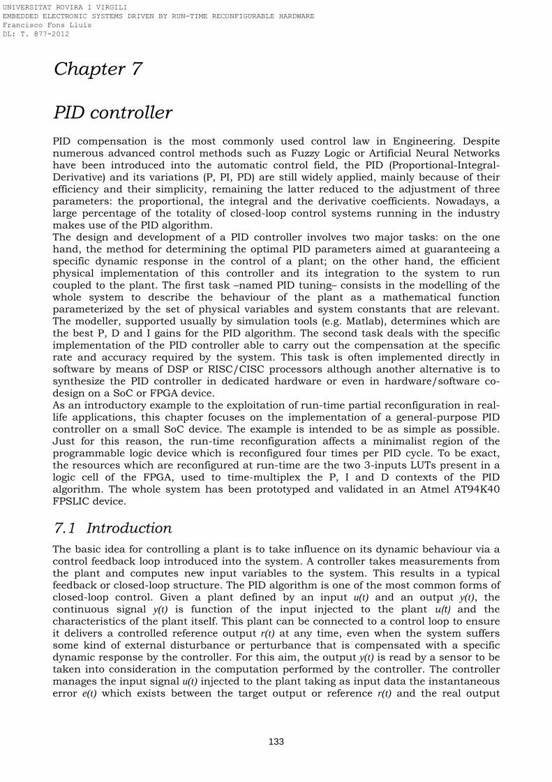
133
Chapter 7
PID controller PID compensation is the most commonly used control law in Engineering. Despite numerous advanced control methods such as Fuzzy Logic or Artificial Neural Networks have been introduced into the automatic control field, the PID (Proportional-Integral-Derivative) and its variations (P, PI, PD) are still widely applied, mainly because of their efficiency and their simplicity, remaining the latter reduced to the adjustment of three parameters: the proportional, the integral and the derivative coefficients. Nowadays, a large percentage of the totality of closed-loop control systems running in the industry makes use of the PID algorithm. The design and development of a PID controller involves two major tasks: on the one hand, the method for determining the optimal PID parameters aimed at guaranteeing a specific dynamic response in the control of a plant; on the other hand, the efficient physical implementation of this controller and its integration to the system to run coupled to the plant. The first task –named PID tuning– consists in the modelling of the whole system to describe the behaviour of the plant as a mathematical function parameterized by the set of physical variables and system constants that are relevant. The modeller, supported usually by simulation tools (e.g. Matlab), determines which are the best P, D and I gains for the PID algorithm. The second task deals with the specific implementation of the PID controller able to carry out the compensation at the specific rate and accuracy required by the system. This task is often implemented directly in software by means of DSP or RISC/CISC processors although another alternative is to synthesize the PID controller in dedicated hardware or even in hardware/software co-design on a SoC or FPGA device. As an introductory example to the exploitation of run-time partial reconfiguration in real-life applications, this chapter focuses on the implementation of a general-purpose PID controller on a small SoC device. The example is intended to be as simple as possible. Just for this reason, the run-time reconfiguration affects a minimalist region of the programmable logic device which is reconfigured four times per PID cycle. To be exact, the resources which are reconfigured at run-time are the two 3-inputs LUTs present in a logic cell of the FPGA, used to time-multiplex the P, I and D contexts of the PID algorithm. The whole system has been prototyped and validated in an Atmel AT94K40 FPSLIC device.
7.1 Introduction
The basic idea for controlling a plant is to take influence on its dynamic behaviour via a control feedback loop introduced into the system. A controller takes measurements from the plant and computes new input variables to the system. This results in a typical feedback or closed-loop structure. The PID algorithm is one of the most common forms of closed-loop control. Given a plant defined by an input u(t) and an output y(t), the continuous signal y(t) is function of the input injected to the plant u(t) and the characteristics of the plant itself. This plant can be connected to a control loop to ensure it delivers a controlled reference output r(t) at any time, even when the system suffers some kind of external disturbance or perturbance that is compensated with a specific dynamic response by the controller. For this aim, the output y(t) is read by a sensor to be taken into consideration in the computation performed by the controller. The controller manages the input signal u(t) injected to the plant taking as input data the instantaneous error e(t) which exists between the target output or reference r(t) and the real output
UNIVERSITAT ROVIRA I VIRGILI EMBEDDED ELECTRONIC SYSTEMS DRIVEN BY RUN-TIME RECONFIGURABLE HARDWARE Francisco Fons Lluís DL: T. 877-2012
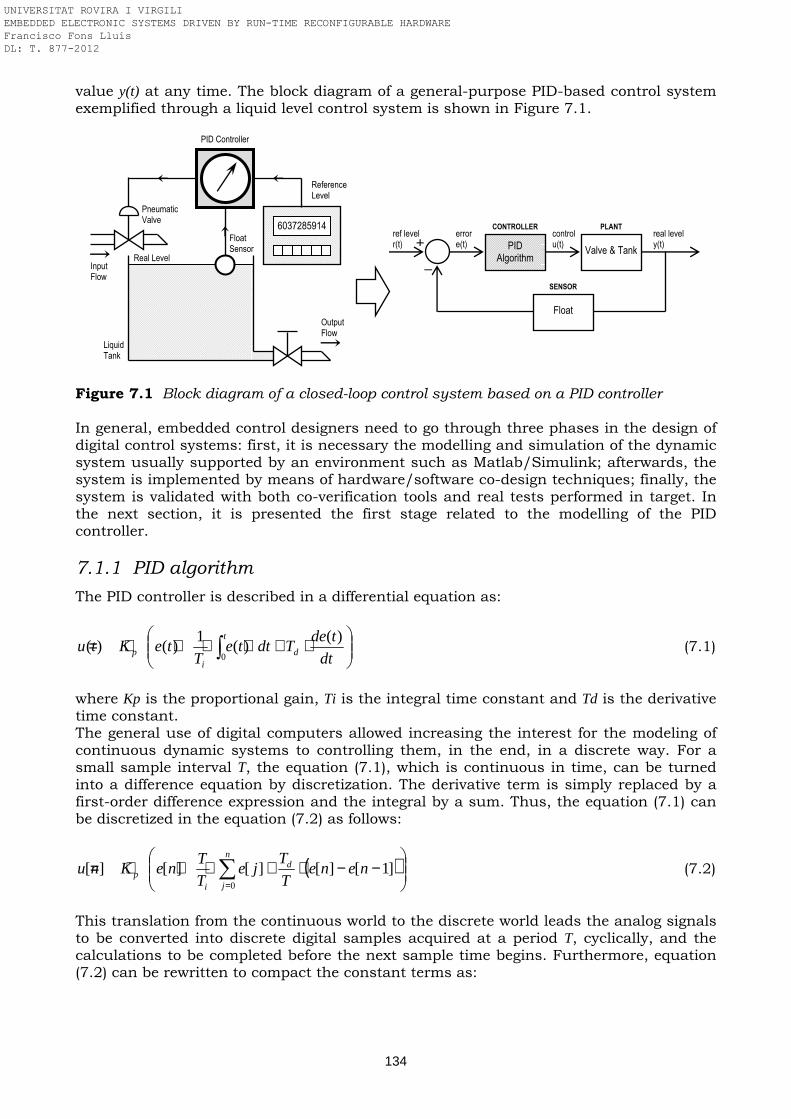
134
value y(t) at any time. The block diagram of a general-purpose PID-based control system exemplified through a liquid level control system is shown in Figure 7.1.
Figure 7.1 Block diagram of a closed-loop control system based on a PID controller In general, embedded control designers need to go through three phases in the design of digital control systems: first, it is necessary the modelling and simulation of the dynamic system usually supported by an environment such as Matlab/Simulink; afterwards, the system is implemented by means of hardware/software co-design techniques; finally, the system is validated with both co-verification tools and real tests performed in target. In the next section, it is presented the first stage related to the modelling of the PID controller.
7.1.1 PID algorithm
The PID controller is described in a differential equation as:
⋅+⋅⋅+⋅= ∫ dt
tdeTdtte
TteKtu d
t
ip
)()(
1)()(
0 (7.1)
where Kp is the proportional gain, Ti is the integral time constant and Td is the derivative time constant. The general use of digital computers allowed increasing the interest for the modeling of continuous dynamic systems to controlling them, in the end, in a discrete way. For a small sample interval T, the equation (7.1), which is continuous in time, can be turned into a difference equation by discretization. The derivative term is simply replaced by a first-order difference expression and the integral by a sum. Thus, the equation (7.1) can be discretized in the equation (7.2) as follows:
( )
−−⋅+⋅+⋅= ∑
=
n
j
d
ip nene
T
Tje
T
TneKnu
0
]1[][][][][ (7.2)
This translation from the continuous world to the discrete world leads the analog signals to be converted into discrete digital samples acquired at a period T, cyclically, and the calculations to be completed before the next sample time begins. Furthermore, equation (7.2) can be rewritten to compact the constant terms as:
PID Algorithm
Valve & Tank
Float
CONTROLLER PLANT
SENSOR
ref level r(t)
error e(t)
control u(t)
real level y(t) +
_
6037285914
Reference Level
Float Sensor
Pneumatic Valve
Liquid Tank
Input Flow
Output Flow
PID Controller
Real Level
UNIVERSITAT ROVIRA I VIRGILI EMBEDDED ELECTRONIC SYSTEMS DRIVEN BY RUN-TIME RECONFIGURABLE HARDWARE Francisco Fons Lluís DL: T. 877-2012
135
( )]1[][][][][0
−−⋅+⋅+⋅= ∑=
neneKjeKneKnu d
n
jip (7.3)
where Ki = Kp·T/Ti is the integral gain, and Kd = Kp·Td/T is the derivative gain. This difference equation can now be easily implemented by a digital system, either in hardware or in software. It is a matter of cyclically acquiring e[n] and performing the products and additions required. The pseudo-code of the PID algorithm is shown next: /* Initialization stage */ Kp = PrpConstant /* Configuration of the proportional gain */ Ki = IntConstant /* Configuration of the integral gain */ Kd = DerConstant /* Configuration of the derivative gain */ Em = 0 /* Error Em=e[n-1] initialized to zero */ SumEm = 0 /* SumEm=e[0]+e[1]+...+e[n-1] initialized to zero */ /* Cyclic operation */ Loop En = error /* Error En=e[n]=r[n]-y[n], acquisition */ Un = Kp·En+Ki·(En+SumEm)+Kd·(En-Em) /* Control Un=u[n], closed-loop control */ SumEm = En+SumEm Em = En Wait T /* Sampling period T */ End loop
Code 7.1 PID algorithm Therefore, the PID controller compensates the error between the desired and the real value of the output signal. The closed loop inserted makes the plant to be self-fed by an input consisting of the sum of three terms: a proportional factor responsible for adjusting the control signal in the same percentage than the instantaneous error, a derivative factor that contributes proportionally to the rate of change of such error, and an integral term with the role of integrating the instantaneous error along the time. In PID control, increasing the proportional gain can increase system response speed and it can decrease steady-state error but not eliminate it completely. Additionally, the performance of the closed-loop system becomes more oscillatory and takes longer to settle down after being disturbed as the gain is increased. To avoid these difficulties, integral control and derivative control can eliminate steady-state error and improve system stability, respectively. Thus, the three terms help to cancel any deviation or disturbance present or appeared at any time in the system and maintain therefore the equilibrium, achieving the tracking of the reference level with a dynamic response in accordance with the fixed characteristics of the whole plant-controller.
7.2 Related work
PID control is widely used in the industry. The implementation of PID controllers has gone through several stages of evolution, from early mechanical and pneumatic designs to microprocessor-based systems. Recently, FPGAs have become an alternative solution for the realization of digital control systems, which were previously dominated by general-purpose microprocessor systems. The PID algorithm has been proposed to be implemented in hardware in many occasions in the literature. This section describes some of these works. Samet et al. do research into three different PID hardware architectures (serial, parallel and mixed) in the XC4000 family of Xilinx FPGA devices [Samet et al., ICECS 1998]. The PID computation time fluctuates from one clock of 220 ns period in the parallel architecture to 28 clock cycles at 120 ns in the serial approach (3360 ns), having as an intermediate solution the mixed architecture that needs 6 clocks at 115 ns (690 ns) to complete the PID computation.
UNIVERSITAT ROVIRA I VIRGILI EMBEDDED ELECTRONIC SYSTEMS DRIVEN BY RUN-TIME RECONFIGURABLE HARDWARE Francisco Fons Lluís DL: T. 877-2012
136
The PID controller presented in [Astarloa et al., IECON 2006] is implemented in a Xilinx Spartan-3 FPGA and integrated in a motor multi-axis control system. The system constitutes a four axis controller and each axis is controlled by a PID unit. A 32-bit host processor manages all the application while four PID controllers take charge of the trajectory managed by four local tiny soft processors. In this system, the PID computation is the most intensive task and is performed in hardware while other less demanding tasks like the trajectory computation are performed in software. The PID controller is implemented in a 3-stages pipeline and the processing of the proportional, integral and derivative terms is performed in parallel by means of three embedded hardware multipliers included in the FPGA. Additionally, the program of the tiny processor and the PID control constants can be replaced using dynamic partial reconfiguration. This reconfiguration is handled by the tiny processor interfaced to the reconfiguration controller. The sampling rate of this system is 50 MHz. Chen et al. implemented a complete electric wheelchair controller on an Altera Flex 10K FPGA device and partitioned in several independent functional blocks [Chen et al., TIE 2000]. The PID control block is the largest block of the system occupying 740 logic cells, figure that represents the 73% of the resources used by the whole system. It constitutes a parallel and pipelined PID controller composed of an accumulator, some registers working as delay elements, four adders and three multipliers. The control cycle is set to 128 Hz. A distributed-arithmetic (DA) based PID controller algorithm is proposed in [Chan et al., TIE 2007] to be applied in a temperature control system. The DA-based PID controller demonstrates 80% savings in hardware utilization and 40% savings in power consumption compared to the multiplier-based scheme. The synthesized DA-based PID is implemented in a Xilinx Spartan-IIE FPGA and allows a maximum clock frequency of 47 MHz with 456 mW power consumption. The frequency and the power consumed by the synthesized multiplier-based PID are 25 MHz and 765 mW, respectively, and it is implemented in a Xilinx Spartan-3 FPGA provided with embedded 18x18 multipliers. It should be noted that, due to the serial nature of the DA method, the DA-based PID controller needs 17 clock cycles or 361 ns computation time while the design using multipliers needs one clock cycle or 67 ns. In [Zhao et al., ICAR 2005], it is researched the design of a digital control system implemented in reconfigurable hardware in a Xilinx Spartan-II FPGA platform and applied to small-scale robots. Specifically, the authors looked at closed-loop proportitonal-integral-derivative control for a robot with high degrees-of-freedom, which when implemented in software requires a lot of CPU time and a real-time operating system. By moving control to hardware, the robot can dedicate the CPU time to other tasks. They analize the different design trade-offs in terms of area, power consumption and execution time. In this work, equation (7.3) is rewritten and implemented as an alternative recursive algorithm where the calculation of u[n] is based on u[n-1]. The authors propose a parallel and a serial design: for the parallel approach, each basic operation has its own arithmetic unit (either an adder or a multiplier) and the design requires four adders and three multipliers in total, apart from registers and other logic that constitutes the datapath; for the serial design, however, all operations share only one adder and one multiplier. As result, the PID computation takes four clocks in a serial approach and one clock in a parallel approach. Nevertheless, the critical path delay of the parallel design is quite long relative to the serial design and it includes the delay of one multiplier and three adders of different operands size. The parallel design is mainly a combinational logic requiring only a single cycle to complete where the delay is around 50 ns so the sampling cycle is set to 20 MHz. In the serial design, thee delay is close to 30 ns and each PID computation requires four cycles so the minimum sampling period results in 120 ns, that is, a sampling frequency of 8.33 MHz. Furthermore, whereas all the prior works are for one channel control, in this work different designs for the closed-loop PID control algorithm are implemented on an FPGA for one channel and also for multiple channels. In multiple-channel design, either a PID unit is dedicated to each
UNIVERSITAT ROVIRA I VIRGILI EMBEDDED ELECTRONIC SYSTEMS DRIVEN BY RUN-TIME RECONFIGURABLE HARDWARE Francisco Fons Lluís DL: T. 877-2012
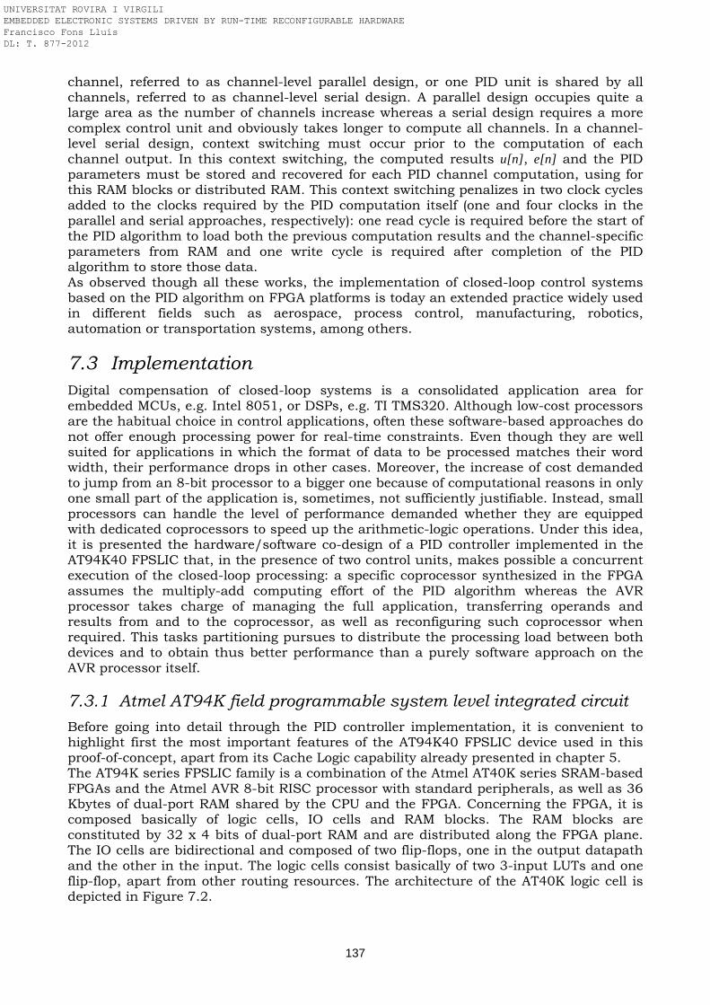
137
channel, referred to as channel-level parallel design, or one PID unit is shared by all channels, referred to as channel-level serial design. A parallel design occupies quite a large area as the number of channels increase whereas a serial design requires a more complex control unit and obviously takes longer to compute all channels. In a channel-level serial design, context switching must occur prior to the computation of each channel output. In this context switching, the computed results u[n] , e[n] and the PID parameters must be stored and recovered for each PID channel computation, using for this RAM blocks or distributed RAM. This context switching penalizes in two clock cycles added to the clocks required by the PID computation itself (one and four clocks in the parallel and serial approaches, respectively): one read cycle is required before the start of the PID algorithm to load both the previous computation results and the channel-specific parameters from RAM and one write cycle is required after completion of the PID algorithm to store those data. As observed though all these works, the implementation of closed-loop control systems based on the PID algorithm on FPGA platforms is today an extended practice widely used in different fields such as aerospace, process control, manufacturing, robotics, automation or transportation systems, among others.
7.3 Implementation
Digital compensation of closed-loop systems is a consolidated application area for embedded MCUs, e.g. Intel 8051, or DSPs, e.g. TI TMS320. Although low-cost processors are the habitual choice in control applications, often these software-based approaches do not offer enough processing power for real-time constraints. Even though they are well suited for applications in which the format of data to be processed matches their word width, their performance drops in other cases. Moreover, the increase of cost demanded to jump from an 8-bit processor to a bigger one because of computational reasons in only one small part of the application is, sometimes, not sufficiently justifiable. Instead, small processors can handle the level of performance demanded whether they are equipped with dedicated coprocessors to speed up the arithmetic-logic operations. Under this idea, it is presented the hardware/software co-design of a PID controller implemented in the AT94K40 FPSLIC that, in the presence of two control units, makes possible a concurrent execution of the closed-loop processing: a specific coprocessor synthesized in the FPGA assumes the multiply-add computing effort of the PID algorithm whereas the AVR processor takes charge of managing the full application, transferring operands and results from and to the coprocessor, as well as reconfiguring such coprocessor when required. This tasks partitioning pursues to distribute the processing load between both devices and to obtain thus better performance than a purely software approach on the AVR processor itself.
7.3.1 Atmel AT94K field programmable system level integrated circuit
Before going into detail through the PID controller implementation, it is convenient to highlight first the most important features of the AT94K40 FPSLIC device used in this proof-of-concept, apart from its Cache Logic capability already presented in chapter 5. The AT94K series FPSLIC family is a combination of the Atmel AT40K series SRAM-based FPGAs and the Atmel AVR 8-bit RISC processor with standard peripherals, as well as 36 Kbytes of dual-port RAM shared by the CPU and the FPGA. Concerning the FPGA, it is composed basically of logic cells, IO cells and RAM blocks. The RAM blocks are constituted by 32 x 4 bits of dual-port RAM and are distributed along the FPGA plane. The IO cells are bidirectional and composed of two flip-flops, one in the output datapath and the other in the input. The logic cells consist basically of two 3-input LUTs and one flip-flop, apart from other routing resources. The architecture of the AT40K logic cell is depicted in Figure 7.2.
UNIVERSITAT ROVIRA I VIRGILI EMBEDDED ELECTRONIC SYSTEMS DRIVEN BY RUN-TIME RECONFIGURABLE HARDWARE Francisco Fons Lluís DL: T. 877-2012
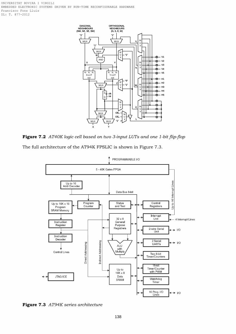
138
YL
WL
ZL
Y
Z
X
XL
X-LUT
D
Q
Y-LUT
MUX
MUX
MUX
MUX
AND
MUX
MUX
MUX
MUX
MUX
MUX
MUX
MUX
MUX
MUX
MUX L
V1
V2
V3
V4
V5
H1
H2
H3
H4
H5
OEV
OEH
“1”
“0”
“1”
“1”
“1”
“1” “1”
ORTHOGONAL NEIGHBOURS
(N, S, E, W)
DIAGONALNEIGHBOURS
(NW, NE, SE, SW)
clkrst
a0 a1 a2 a2 a1 a0
outout
X Y
W
YL
WL
ZL
Y
Z
X
XL
X-LUT
D
Q
Y-LUT
MUX
MUX
MUX
MUX
AND
MUX
MUX
MUX
MUX
MUX
MUX
MUX
MUX
MUX
MUX
MUX L
V1
V2
V3
V4
V5
H1
H2
H3
H4
H5
OEV
OEH
“1”
“0”
“1”
“1”
“1”
“1” “1”
ORTHOGONAL NEIGHBOURS
(N, S, E, W)
DIAGONALNEIGHBOURS
(NW, NE, SE, SW)
clkrst
a0 a1 a2 a2 a1 a0
outout
X Y
W
Figure 7.2 AT40K logic cell based on two 3-input LUTs and one 1-bit flip-flop The full architecture of the AT94K FPSLIC is shown in Figure 7.3.
Figure 7.3 AT94K series architecture
UNIVERSITAT ROVIRA I VIRGILI EMBEDDED ELECTRONIC SYSTEMS DRIVEN BY RUN-TIME RECONFIGURABLE HARDWARE Francisco Fons Lluís DL: T. 877-2012
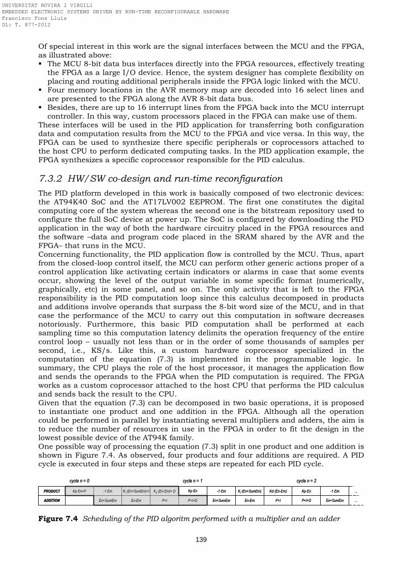
139
Of special interest in this work are the signal interfaces between the MCU and the FPGA, as illustrated above: The MCU 8-bit data bus interfaces directly into the FPGA resources, effectively treating
the FPGA as a large I/O device. Hence, the system designer has complete flexibility on placing and routing additional peripherals inside the FPGA logic linked with the MCU.
Four memory locations in the AVR memory map are decoded into 16 select lines and are presented to the FPGA along the AVR 8-bit data bus.
Besides, there are up to 16 interrupt lines from the FPGA back into the MCU interrupt controller. In this way, custom processors placed in the FPGA can make use of them.
These interfaces will be used in the PID application for transferring both configuration data and computation results from the MCU to the FPGA and vice versa. In this way, the FPGA can be used to synthesize there specific peripherals or coprocessors attached to the host CPU to perform dedicated computing tasks. In the PID application example, the FPGA synthesizes a specific coprocessor responsible for the PID calculus.
7.3.2 HW/SW co-design and run-time reconfiguration
The PID platform developed in this work is basically composed of two electronic devices: the AT94K40 SoC and the AT17LV002 EEPROM. The first one constitutes the digital computing core of the system whereas the second one is the bitstream repository used to configure the full SoC device at power up. The SoC is configured by downloading the PID application in the way of both the hardware circuitry placed in the FPGA resources and the software –data and program code placed in the SRAM shared by the AVR and the FPGA– that runs in the MCU. Concerning functionality, the PID application flow is controlled by the MCU. Thus, apart from the closed-loop control itself, the MCU can perform other generic actions proper of a control application like activating certain indicators or alarms in case that some events occur, showing the level of the output variable in some specific format (numerically, graphically, etc) in some panel, and so on. The only activity that is left to the FPGA responsibility is the PID computation loop since this calculus decomposed in products and additions involve operands that surpass the 8-bit word size of the MCU, and in that case the performance of the MCU to carry out this computation in software decreases notoriously. Furthermore, this basic PID computation shall be performed at each sampling time so this computation latency delimits the operation frequency of the entire control loop – usually not less than or in the order of some thousands of samples per second, i.e., KS/s. Like this, a custom hardware coprocessor specialized in the computation of the equation (7.3) is implemented in the programmable logic. In summary, the CPU plays the role of the host processor, it manages the application flow and sends the operands to the FPGA when the PID computation is required. The FPGA works as a custom coprocessor attached to the host CPU that performs the PID calculus and sends back the result to the CPU. Given that the equation (7.3) can be decomposed in two basic operations, it is proposed to instantiate one product and one addition in the FPGA. Although all the operation could be performed in parallel by instantiating several multipliers and adders, the aim is to reduce the number of resources in use in the FPGA in order to fit the design in the lowest possible device of the AT94K family. One possible way of processing the equation (7.3) split in one product and one addition is shown in Figure 7.4. As observed, four products and four additions are required. A PID cycle is executed in four steps and these steps are repeated for each PID cycle.
Figure 7.4 Scheduling of the PID algoritm performed with a multiplier and an adder
En+SumEmP+I+D
cycle n = 0
KpEn=P -1Em Ki(En+SumEm)=I Kd(En-Em)= D
En+SumEm En-Em
PRODUCT
ADDITION P+I
KpEn -1Em Ki(En+SumEm) Kd(En-Em)
En-Em P+I P+I+D
KpEn -1Em
En+SumEm ...
...
cycle n = 1 cycle n = 2
En+SumEmP+I+D
cycle n = 0
KpEn=P -1Em Ki(En+SumEm)=I Kd(En-Em)= D
En+SumEm En-Em
PRODUCT
ADDITION P+I
KpEn -1Em Ki(En+SumEm) Kd(En-Em)
En-Em P+I P+I+D
KpEn -1Em
En+SumEm ...
...
cycle n = 1 cycle n = 2
UNIVERSITAT ROVIRA I VIRGILI EMBEDDED ELECTRONIC SYSTEMS DRIVEN BY RUN-TIME RECONFIGURABLE HARDWARE Francisco Fons Lluís DL: T. 877-2012
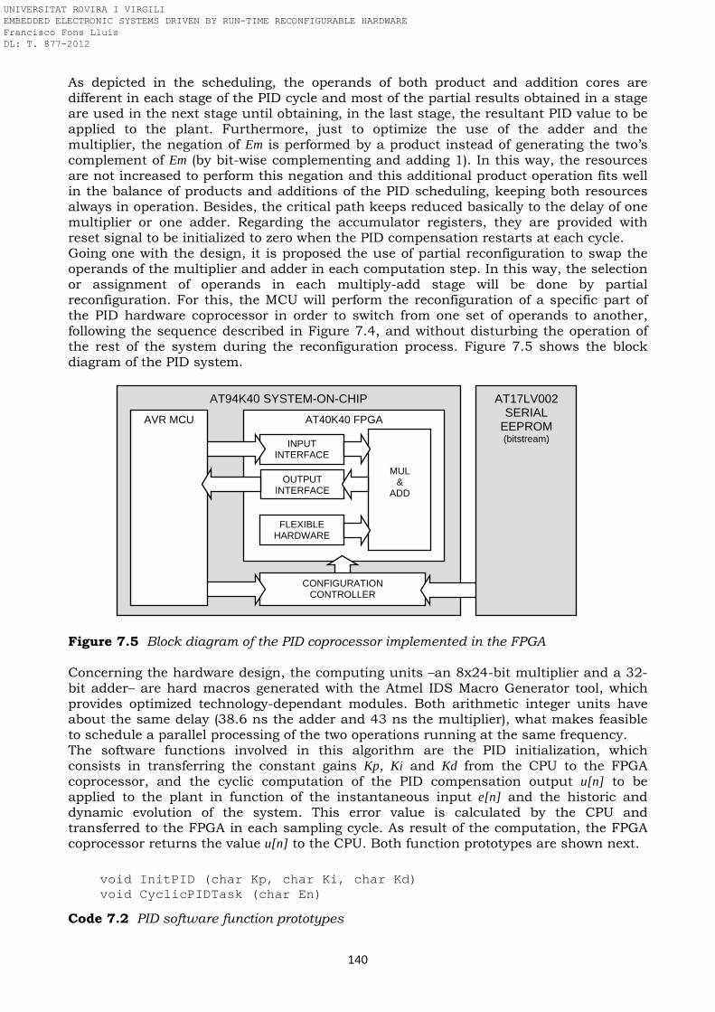
140
As depicted in the scheduling, the operands of both product and addition cores are different in each stage of the PID cycle and most of the partial results obtained in a stage are used in the next stage until obtaining, in the last stage, the resultant PID value to be applied to the plant. Furthermore, just to optimize the use of the adder and the multiplier, the negation of Em is performed by a product instead of generating the two’s complement of Em (by bit-wise complementing and adding 1). In this way, the resources are not increased to perform this negation and this additional product operation fits well in the balance of products and additions of the PID scheduling, keeping both resources always in operation. Besides, the critical path keeps reduced basically to the delay of one multiplier or one adder. Regarding the accumulator registers, they are provided with reset signal to be initialized to zero when the PID compensation restarts at each cycle. Going one with the design, it is proposed the use of partial reconfiguration to swap the operands of the multiplier and adder in each computation step. In this way, the selection or assignment of operands in each multiply-add stage will be done by partial reconfiguration. For this, the MCU will perform the reconfiguration of a specific part of the PID hardware coprocessor in order to switch from one set of operands to another, following the sequence described in Figure 7.4, and without disturbing the operation of the rest of the system during the reconfiguration process. Figure 7.5 shows the block diagram of the PID system. Figure 7.5 Block diagram of the PID coprocessor implemented in the FPGA Concerning the hardware design, the computing units –an 8x24-bit multiplier and a 32-bit adder– are hard macros generated with the Atmel IDS Macro Generator tool, which provides optimized technology-dependant modules. Both arithmetic integer units have about the same delay (38.6 ns the adder and 43 ns the multiplier), what makes feasible to schedule a parallel processing of the two operations running at the same frequency. The software functions involved in this algorithm are the PID initialization, which consists in transferring the constant gains Kp, Ki and Kd from the CPU to the FPGA coprocessor, and the cyclic computation of the PID compensation output u[n] to be applied to the plant in function of the instantaneous input e[n] and the historic and dynamic evolution of the system. This error value is calculated by the CPU and transferred to the FPGA in each sampling cycle. As result of the computation, the FPGA coprocessor returns the value u[n] to the CPU. Both function prototypes are shown next.
void InitPID (char Kp, char Ki, char Kd) void CyclicPIDTask (char En)
Code 7.2 PID software function prototypes
AT94K40 SYSTEM-ON-CHIP
AT40K40 FPGA
MUL &
ADD
INPUT INTERFACE
OUTPUT INTERFACE
FLEXIBLE HARDWARE
CONFIGURATION CONTROLLER
AT17LV002 SERIAL
EEPROM (bitstream)
AVR MCU
UNIVERSITAT ROVIRA I VIRGILI EMBEDDED ELECTRONIC SYSTEMS DRIVEN BY RUN-TIME RECONFIGURABLE HARDWARE Francisco Fons Lluís DL: T. 877-2012
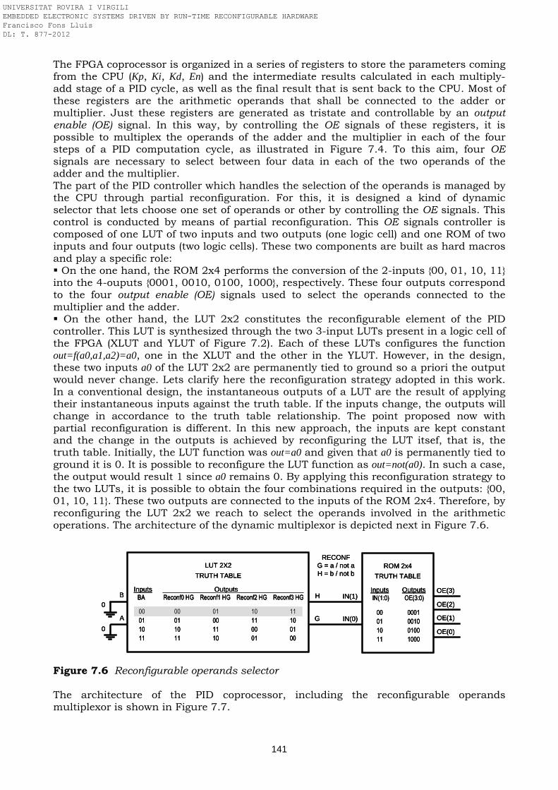
141
The FPGA coprocessor is organized in a series of registers to store the parameters coming from the CPU (Kp, Ki, Kd, En) and the intermediate results calculated in each multiply-add stage of a PID cycle, as well as the final result that is sent back to the CPU. Most of these registers are the arithmetic operands that shall be connected to the adder or multiplier. Just these registers are generated as tristate and controllable by an output enable (OE) signal. In this way, by controlling the OE signals of these registers, it is possible to multiplex the operands of the adder and the multiplier in each of the four steps of a PID computation cycle, as illustrated in Figure 7.4. To this aim, four OE signals are necessary to select between four data in each of the two operands of the adder and the multiplier. The part of the PID controller which handles the selection of the operands is managed by the CPU through partial reconfiguration. For this, it is designed a kind of dynamic selector that lets choose one set of operands or other by controlling the OE signals. This control is conducted by means of partial reconfiguration. This OE signals controller is composed of one LUT of two inputs and two outputs (one logic cell) and one ROM of two inputs and four outputs (two logic cells). These two components are built as hard macros and play a specific role: On the one hand, the ROM 2x4 performs the conversion of the 2-inputs 00, 01, 10, 11 into the 4-ouputs 0001, 0010, 0100, 1000, respectively. These four outputs correspond to the four output enable (OE) signals used to select the operands connected to the multiplier and the adder. On the other hand, the LUT 2x2 constitutes the reconfigurable element of the PID controller. This LUT is synthesized through the two 3-input LUTs present in a logic cell of the FPGA (XLUT and YLUT of Figure 7.2). Each of these LUTs configures the function out=f(a0,a1,a2)=a0, one in the XLUT and the other in the YLUT. However, in the design, these two inputs a0 of the LUT 2x2 are permanently tied to ground so a priori the output would never change. Lets clarify here the reconfiguration strategy adopted in this work. In a conventional design, the instantaneous outputs of a LUT are the result of applying their instantaneous inputs against the truth table. If the inputs change, the outputs will change in accordance to the truth table relationship. The point proposed now with partial reconfiguration is different. In this new approach, the inputs are kept constant and the change in the outputs is achieved by reconfiguring the LUT itsef, that is, the truth table. Initially, the LUT function was out=a0 and given that a0 is permanently tied to ground it is 0. It is possible to reconfigure the LUT function as out=not(a0). In such a case, the output would result 1 since a0 remains 0. By applying this reconfiguration strategy to the two LUTs, it is possible to obtain the four combinations required in the outputs: 00, 01, 10, 11. These two outputs are connected to the inputs of the ROM 2x4. Therefore, by reconfiguring the LUT 2x2 we reach to select the operands involved in the arithmetic operations. The architecture of the dynamic multiplexor is depicted next in Figure 7.6.
Figure 7.6 Reconfigurable operands selector The architecture of the PID coprocessor, including the reconfigurable operands multiplexor is shown in Figure 7.7.
LUT 2X2
TRUTH TABLE
Inputs OutputsBA Reconf0 HG Reconf1 HG Reconf2 HG Reconf3 HG
00 00 01 10 1101 01 00 11 1010 10 11 00 0111 11 10 01 00
ROM 2x4
TRUTH TABLE
Inputs OutputsIN(1:0) OE(3:0)
00 000101 001010 010011 1000
OE(3)
OE(2)
OE(1)
OE(0)
IN(1)
IN(0)
B
A
H
G
RECONFG = a / not aH = b / not b
0
0
LUT 2X2
TRUTH TABLE
Inputs OutputsBA Reconf0 HG Reconf1 HG Reconf2 HG Reconf3 HG
00 00 01 10 1101 01 00 11 1010 10 11 00 0111 11 10 01 00
ROM 2x4
TRUTH TABLE
Inputs OutputsIN(1:0) OE(3:0)
00 000101 001010 010011 1000
OE(3)
OE(2)
OE(1)
OE(0)
IN(1)
IN(0)
B
A
H
G
RECONFG = a / not aH = b / not b
0
0
LUT 2X2
TRUTH TABLE
Inputs OutputsBA Reconf0 HG Reconf1 HG Reconf2 HG Reconf3 HG
00 00 01 10 1101 01 00 11 1010 10 11 00 0111 11 10 01 00
ROM 2x4
TRUTH TABLE
Inputs OutputsIN(1:0) OE(3:0)
00 000101 001010 010011 1000
OE(3)
OE(2)
OE(1)
OE(0)
IN(1)
IN(0)
B
A
H
G
RECONFG = a / not aH = b / not b
0
0
UNIVERSITAT ROVIRA I VIRGILI EMBEDDED ELECTRONIC SYSTEMS DRIVEN BY RUN-TIME RECONFIGURABLE HARDWARE Francisco Fons Lluís DL: T. 877-2012
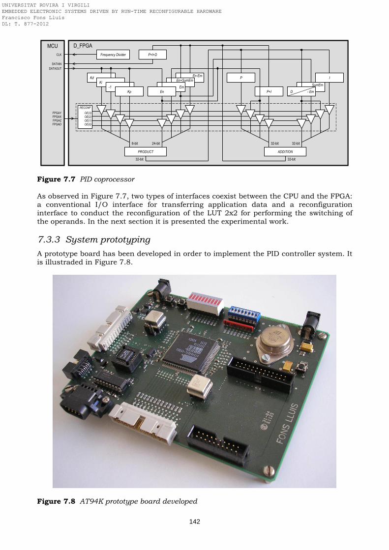
142
Figure 7.7 PID coprocessor As observed in Figure 7.7, two types of interfaces coexist between the CPU and the FPGA: a conventional I/O interface for transferring application data and a reconfiguration interface to conduct the reconfiguration of the LUT 2x2 for performing the switching of the operands. In the next section it is presented the experimental work.
7.3.3 System prototyping
A prototype board has been developed in order to implement the PID controller system. It is illustraded in Figure 7.8.
Figure 7.8 AT94K prototype board developed
En-Em
MCU
PRODUCT
Kd
ADDITION
I
RECONF
Frequency Divider
D_FPGA
Ki
-1
Kp
En+SumEm
Em
En P+I
P
SumEm
D
P+I+D
8-bit 24-bit
32-bit
32-bit 32-bit
32-bit
CLK
DATAIN
DATAOUT
FPGAYFPGAXFPGAZFPGAD
- Em
OE(3)
OE(2)
OE(1)
OE(0)
En-Em
MCU
PRODUCT
Kd
ADDITION
I
RECONF
Frequency Divider
D_FPGA
Ki
-1
Kp
En+SumEm
Em
En P+I
P
SumEm
D
P+I+D
8-bit 24-bit
32-bit
32-bit 32-bit
32-bit
CLK
DATAIN
DATAOUT
FPGAYFPGAXFPGAZFPGAD
- Em
OE(3)
OE(2)
OE(1)
OE(0)
UNIVERSITAT ROVIRA I VIRGILI EMBEDDED ELECTRONIC SYSTEMS DRIVEN BY RUN-TIME RECONFIGURABLE HARDWARE Francisco Fons Lluís DL: T. 877-2012
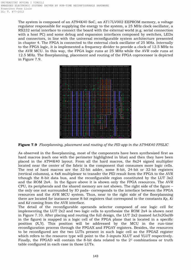
143
The system is composed of an AT94K40 SoC, an AT17LV002 EEPROM memory, a voltage regulator responsible for supplying the energy to the system, a 25 MHz clock oscillator, a RS232 serial interface to connect the board with the external world (e.g. serial connection with a host PC) and some debug and expansion interfaces composed by switches, LEDs and connectors, in line with the universal reconfigurable system architecture presented in chapter 4. The FPGA is connected to the external clock oscillator of 25 MHz. Internally to the FPGA logic, it is implemented a frequency divider to provide a clock of 12.5 MHz to the AVR MCU. In this way, the FPGA logic runs at 25 MHz while the AVR code runs at 12.5 MHz. The floorplanning, placement and routing of the FPGA coprocessor is depicted in Figure 7.9.
Figure 7.9 Floorplanning, placement and routing of the PID app in the AT94K40 FPSLIC As observed in the floorplanning, most of the components have been synthesized first as hard macros (each one with the perimeter highlighted in blue) and then they have been placed in the AT94K40 layout. From all the hard macros, the 8x24 signed multiplier located near the center of the fabric is the component that consumes more logic cells. The rest of hard macros are the 32-bit adder, some 8-bit, 24-bit or 32-bit registers (vertical columns), a 4x8 multiplexor to transfer the PID result form the FPGA to the AVR trhough the 8-bit data bus, and the reconfigurable region constituted by the LUT 3x2 and the ROM 2x4. In the figure above it is shown only the FPGA resources. The AVR CPU, its peripherals and the shared memory are not shown. The right side of the figure –the only one not surrounded by IO pads– corresponds to the interface between the FPGA resources and the AVR MCU system. Thus, near to the right side of the floorplanning there are located for instance some 8-bit registers that correspond to the constants Kp, Ki and Kd coming from the AVR interface. The detail of the reconfigurable operands selector composed of one logic cell for implementing the LUT 2x2 and two logic cells to synthesize the ROM 2x4 is shown next in Figure 7.10. After placing and routing the full design, the LUT 2x2 (named lut3x2GaHb in the figure) is mapped in a logic cell of the FPGA plane that is located in a specific position (X,Y). This position will be addressed by the MCU in the run-time reconfiguration process through the FPGAX and FPGAY registers. Besides, the resources to be reconfigured are the two LUTs present in such logic cell so the FPGAZ register which refers to the resource type will point to the 3-inputs XLUT and YLUT respectively. Finally, the FPGAD will contain the 8-bit data related to the 23 combinations or truth table configured in each case in those LUTs.
UNIVERSITAT ROVIRA I VIRGILI EMBEDDED ELECTRONIC SYSTEMS DRIVEN BY RUN-TIME RECONFIGURABLE HARDWARE Francisco Fons Lluís DL: T. 877-2012
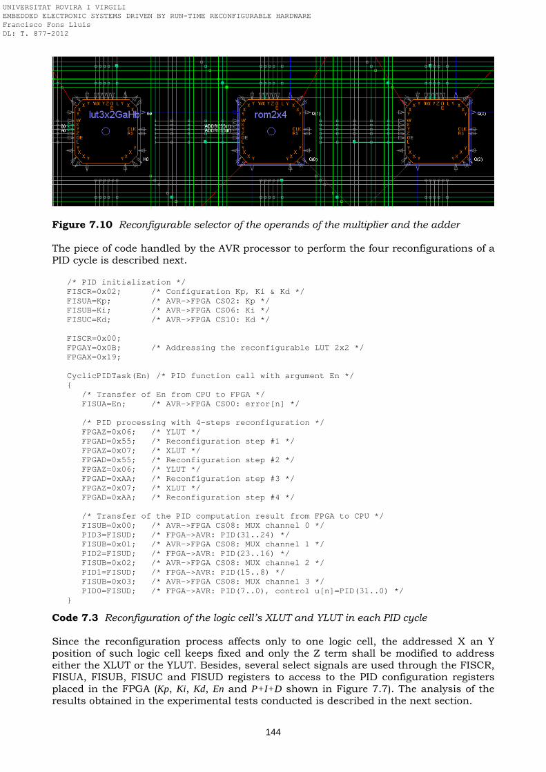
144
Figure 7.10 Reconfigurable selector of the operands of the multiplier and the adder The piece of code handled by the AVR processor to perform the four reconfigurations of a PID cycle is described next. /* PID initialization */ FISCR=0x02; /* Configuration Kp, Ki & Kd */ FISUA=Kp; /* AVR->FPGA CS02: Kp */ FISUB=Ki; /* AVR->FPGA CS06: Ki */ FISUC=Kd; /* AVR->FPGA CS10: Kd */ FISCR=0x00; FPGAY=0x0B; /* Addressing the reconfigurable LUT 2x2 */ FPGAX=0x19; CyclicPIDTask(En) /* PID function call with argument En */ /* Transfer of En from CPU to FPGA */ FISUA=En; /* AVR->FPGA CS00: error[n] */ /* PID processing with 4-steps reconfiguration */ FPGAZ=0x06; /* YLUT */ FPGAD=0x55; /* Reconfiguration step #1 */ FPGAZ=0x07; /* XLUT */ FPGAD=0x55; /* Reconfiguration step #2 */ FPGAZ=0x06; /* YLUT */ FPGAD=0xAA; /* Reconfiguration step #3 */ FPGAZ=0x07; /* XLUT */ FPGAD=0xAA; /* Reconfiguration step #4 */ /* Transfer of the PID computation result from FPGA to CPU */ FISUB=0x00; /* AVR->FPGA CS08: MUX channel 0 */ PID3=FISUD; /* FPGA->AVR: PID(31..24) */ FISUB=0x01; /* AVR->FPGA CS08: MUX channel 1 */ PID2=FISUD; /* FPGA->AVR: PID(23..16) */ FISUB=0x02; /* AVR->FPGA CS08: MUX channel 2 */ PID1=FISUD; /* FPGA->AVR: PID(15..8) */ FISUB=0x03; /* AVR->FPGA CS08: MUX channel 3 */ PID0=FISUD; /* FPGA->AVR: PID(7..0), control u[n]=PID(31..0) */
Code 7.3 Reconfiguration of the logic cell’s XLUT and YLUT in each PID cycle Since the reconfiguration process affects only to one logic cell, the addressed X an Y position of such logic cell keeps fixed and only the Z term shall be modified to address either the XLUT or the YLUT. Besides, several select signals are used through the FISCR, FISUA, FISUB, FISUC and FISUD registers to access to the PID configuration registers placed in the FPGA (Kp, Ki, Kd, En and P+I+D shown in Figure 7.7). The analysis of the results obtained in the experimental tests conducted is described in the next section.
UNIVERSITAT ROVIRA I VIRGILI EMBEDDED ELECTRONIC SYSTEMS DRIVEN BY RUN-TIME RECONFIGURABLE HARDWARE Francisco Fons Lluís DL: T. 877-2012
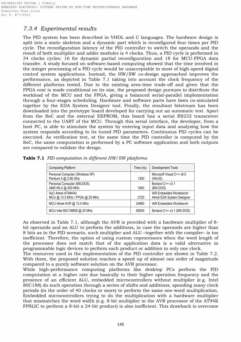
145
7.3.4 Experimental results
The PID system has been described in VHDL and C languages. The hardware design is split into a static skeleton and a dynamic part which is reconfigured four times per PID cycle. The reconfiguration latency of the PID controller to switch the operands and the result of both multiplier and adder modules is 4 clocks. Thus, a PID cycle is performed in 34 clocks cycles: 16 for dynamic partial reconfiguration and 18 for MCU-FPGA data transfer. A study focused on software-based computing showed that the time involved in the integer processing of a PID cycle would be unacceptable in most of high-speed digital control system applications. Instead, the HW/SW co-design approached improves the performance, as depicted in Table 7.1 taking into account the clock frequency of the different platforms tested. Due to the existing area-time trade-off and given that the FPGA cost is made conditional on its size, the proposed design pursues to distribute the workload of the MCU and the FPGA, giving a balanced serial-parallel implementation through a four-stages scheduling. Hardware and software parts have been co-simulated together by the EDA System Designer tool. Finally, the resultant bitstream has been downloaded into the prototype board developed for carrying out an automatic test. Apart from the SoC and the external EEPROM, this board has a serial RS232 transceiver connected to the UART of the MCU. Through this serial interface, the developer, from a host PC, is able to stimulate the system by entering input data and analyzing how the system responds according to its tuned PID parameters. Continuous PID cycles can be executed. As verification test, at the same time the PID controller is computed by the SoC, the same computation is performed by a PC software application and both outputs are compared to validate the design. Table 7.1 PID computation in different HW/SW platforms
Computing Platform Time (ns) Development Tools
Personal Computer (Windows XP) Pentium 4 @ 2.66 GHz
1350
Microsoft Visual C++ v6.0 (Win32)
Personal Computer (MS-DOS) AMD K6-2 @ 450 MHz
1840
Borland C++ v3.1 (MS-DOS)
SoC Atmel AT94K40 MCU @ 12.5 MHz / FPGA @ 25 MHz
2720
IAR Embedded Workbench Atmel EDA System Designer
MCU Atmel AVR @ 12.5 MHz 24960 IAR Embedded Workbench
MCU Intel 80C188EB @ 25 MHz 58000 Borland C++ v3.1 (MS-DOS)
As observed in Table 7.1, although the AVR is provided with a hardware multiplier of 8-bit operands and an ALU to perform the additions, in case the operands are higher than 8 bits as in the PID scenario, such multiplier and ALU –together with the compiler– is too inefficient. Therefore, the option of using custom coprocessors when the word length of the processor does not match that of the application data is a valid alternative in programmable logic devices to perform each product or addition in only one clock. The resources used in the implementation of the PID controller are shown in Table 7.2. With them, the proposed solution reaches a speed up of almost one order of magnitude compared to a purely software solution on the AVR processor. While high-performance computing platforms like desktop PCs perform the PID computation at a higher rate due basically to their higher operation frequency and the presence of an efficient ALU, embedded microcontrollers without multiplier (e.g. Intel 80C188) do such operation through a series of shifts and additions, spending many clock periods (in the order of 40 clocks or more) to perform the same one-word multiplication. Embedded microcontrollers trying to do the multiplication with a hardware multiplier that mismatches the word width (e.g. 8-bit multiplier in the AVR processor of the AT94K FPSLIC to perform a 8-bit x 24-bit product) is also inefficient. This drawback is overcome
UNIVERSITAT ROVIRA I VIRGILI EMBEDDED ELECTRONIC SYSTEMS DRIVEN BY RUN-TIME RECONFIGURABLE HARDWARE Francisco Fons Lluís DL: T. 877-2012
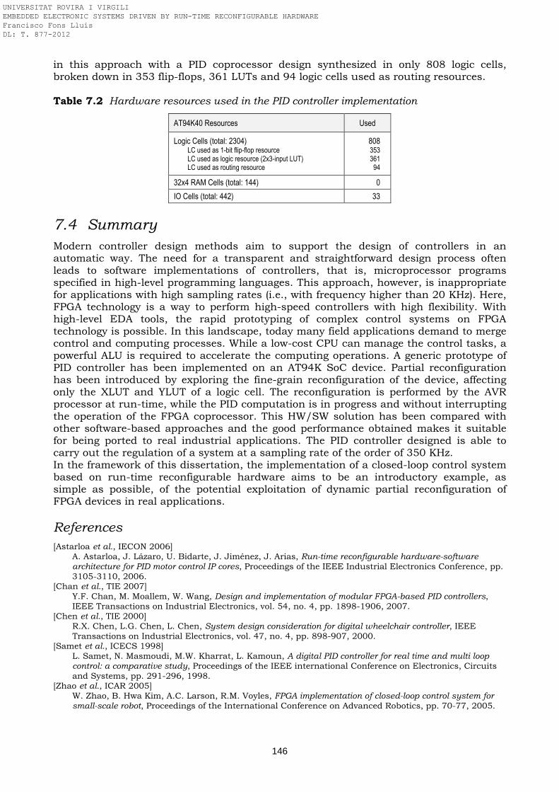
146
in this approach with a PID coprocessor design synthesized in only 808 logic cells, broken down in 353 flip-flops, 361 LUTs and 94 logic cells used as routing resources. Table 7.2 Hardware resources used in the PID controller implementation
AT94K40 Resources Used
Logic Cells (total: 2304) LC used as 1-bit flip-flop resource LC used as logic resource (2x3-input LUT) LC used as routing resource
808 353 361
94
32x4 RAM Cells (total: 144) 0
IO Cells (total: 442) 33
7.4 Summary
Modern controller design methods aim to support the design of controllers in an automatic way. The need for a transparent and straightforward design process often leads to software implementations of controllers, that is, microprocessor programs specified in high-level programming languages. This approach, however, is inappropriate for applications with high sampling rates (i.e., with frequency higher than 20 KHz). Here, FPGA technology is a way to perform high-speed controllers with high flexibility. With high-level EDA tools, the rapid prototyping of complex control systems on FPGA technology is possible. In this landscape, today many field applications demand to merge control and computing processes. While a low-cost CPU can manage the control tasks, a powerful ALU is required to accelerate the computing operations. A generic prototype of PID controller has been implemented on an AT94K SoC device. Partial reconfiguration has been introduced by exploring the fine-grain reconfiguration of the device, affecting only the XLUT and YLUT of a logic cell. The reconfiguration is performed by the AVR processor at run-time, while the PID computation is in progress and without interrupting the operation of the FPGA coprocessor. This HW/SW solution has been compared with other software-based approaches and the good performance obtained makes it suitable for being ported to real industrial applications. The PID controller designed is able to carry out the regulation of a system at a sampling rate of the order of 350 KHz. In the framework of this dissertation, the implementation of a closed-loop control system based on run-time reconfigurable hardware aims to be an introductory example, as simple as possible, of the potential exploitation of dynamic partial reconfiguration of FPGA devices in real applications.
References
[Astarloa et al., IECON 2006] A. Astarloa, J. Lázaro, U. Bidarte, J. Jiménez, J. Arias, Run-time reconfigurable hardware-software architecture for PID motor control IP cores, Proceedings of the IEEE Industrial Electronics Conference, pp. 3105-3110, 2006.
[Chan et al., TIE 2007] Y.F. Chan, M. Moallem, W. Wang, Design and implementation of modular FPGA-based PID controllers, IEEE Transactions on Industrial Electronics, vol. 54, no. 4, pp. 1898-1906, 2007.
[Chen et al., TIE 2000] R.X. Chen, L.G. Chen, L. Chen, System design consideration for digital wheelchair controller, IEEE Transactions on Industrial Electronics, vol. 47, no. 4, pp. 898-907, 2000.
[Samet et al., ICECS 1998] L. Samet, N. Masmoudi, M.W. Kharrat, L. Kamoun, A digital PID controller for real time and multi loop control: a comparative study, Proceedings of the IEEE international Conference on Electronics, Circuits and Systems, pp. 291-296, 1998.
[Zhao et al., ICAR 2005] W. Zhao, B. Hwa Kim, A.C. Larson, R.M. Voyles, FPGA implementation of closed-loop control system for small-scale robot, Proceedings of the International Conference on Advanced Robotics, pp. 70-77, 2005.
UNIVERSITAT ROVIRA I VIRGILI EMBEDDED ELECTRONIC SYSTEMS DRIVEN BY RUN-TIME RECONFIGURABLE HARDWARE Francisco Fons Lluís DL: T. 877-2012
147
Chapter 8 Fuzzy logic controller Fuzzy Logic is a control technique widely extended today in nonlinear control system applications. The facility of fuzzy logic controllers (FLCs) to capture the knowledge of human experts and translate it into robust control strategies without the need of a mathematical model of the plant has led to a significant increase in the number of control applications using fuzzy inference techniques in the last decades. These fuzzy control systems can be implemented following different approaches, ranging from fully software or hardware solutions to hybrid strategies that allow reaching adequate trade-offs between flexibility and inference speed. Hybrid realizations require a processor for software tasks execution and dedicated hardware for implementing complex time-consuming tasks, i.e., typically the fuzzy inference process. This work adds a new point-of-view to the continuous efforts in search of an optimized hardware-software co-design of a dual-input single-output fuzzy logic controller. Our approach breaks up with the classical three-stage implementation process –fuzzification, fuzzy rule inference and defuzzification cores– to focus it on directly synthesizing the resultant control surface. An innovative design methodology is defined by firstly splitting the total area in rectangular sectors to, afterwards, model each of them by second-order polynomial functions. The algorithm is finally embedded in an MCU-FPGA platform to achieve a balanced cost-performance solution inspired by efficient concepts in terms of run-time and silicon-area as parallel processing and dynamic partial reconfiguration, respectively. The result is a standard FLC where the control surface is parameterized and handled through a simple data file appended to the design bitstream in the way of initialized SRAM memory. This HW/SW architecture therefore provides a general-purpose solution able to customize whichever fuzzy application by only updating the data which model the particular control surface segmented in rectangular sectors.
8.1 Introduction
Fuzzy Logic theory, formally introduced in 1965 by Lotfi A. Zadeh, has been successfully applied to many engineering problems from its birth until today [Zadeh, IC 1965]. It emerges as a really useful alternative in those scenarios where the mathematical model of the system is either unattainable or, on the contrary, in spite of reaching it, its inherent complexity makes unsuitable its use. In recent years, this technique has become more and more popular mainly because of two reasons: it offers a universal solution to convert human knowledge into functional rules that, even though they handle imprecise information, may give rise to accurate results; in addition, the intuitive reasoning methodology in which it is inspired allows the easy interpretation and traceability of these results. The mathematical framework of fuzzy inference techniques provides systematic and deterministic algorithms that can be easily described with high-level programming languages or implemented as electronic circuits. Thus, there are basically two alternatives for fuzzy controller implementation: one based on software and the other on hardware, apart from the co-design of both hardware and software together. Software solutions offer flexibility as one of their main features (the designer can choose any type of fuzzy sets, operators, and rules). For this reason, many of the first fuzzy controllers were implemented in software on general-purpose computers. In applications in which size, weight, power, or cost are constrained, as occurs with consumer electronics, standard microcontrollers have been usually employed. The main drawback of software implementations of FLCs is speed limitation due to the sequential program execution and
UNIVERSITAT ROVIRA I VIRGILI EMBEDDED ELECTRONIC SYSTEMS DRIVEN BY RUN-TIME RECONFIGURABLE HARDWARE Francisco Fons Lluís DL: T. 877-2012
148
the fact that standard processors do not directly support many fuzzy operations. In order to reduce the lack of fuzzy operations, some MCUs like the Motorola MC68HC12 and the ST FIVE 508 family from ST Microelectronics modified the architecture of standard processors to support fuzzy computation. Although the specific hardware added to these commercial devices speeds up fuzzy computation by at least one order of magnitude over standard processors, these software solutions are still not fast enough for some time-critical applications, where a dedicated hardware structure must be used. The first hardware implementations of a FLC were the full-custom digital design reported in 1986 at AT&T Bell Laboratories [Togai and Watanabe, Expert 1986] and the analog implementation of Yamagawa and Miki based on the standard CMOS process in nonlinear analog current-mode circuits [Yamakawa and Miki, TC 1986]. Since then, many microelectronic implementations of fuzzy controllers have emerged. Both digital and analog design techniques have been employed, with the digital approaches being the most widely used due to the availability of well-established design methodologies and CAD tools. In order to accelerate fuzzy computation, many hardware solutions implement the inference module or some of its units on a dedicated integrated circuit, so they need to be connected to a general-purpose processing system to complete their operation. These hardware implementations, known as fuzzy accelerators or fuzzy coprocessors, were very popular at the end of the 1990s. Some examples of commercially available fuzzy coprocessors are the SAE 81C99 and SAE 81C991 families from Siemens or the FP1000, FP3000, and FP5000 fuzzy coprocessors from Omron. Nowadays, fuzzy coprocessors are seldom used, and most of them have disappeared from the market as a consequence of the increasing speed of conventional processors, which makes possible to execute the simple fuzzy algorithms required by many applications. Recent advances in silicon technologies allow integrating a complex fuzzy logic control system on a single chip. The rapid evolution of silicon technologies has allowed that programmable logic devices reduce their die sizes and therefore their cost, so hardware platforms like FPGAs can be used not only as rapid prototyping approaches but also as final solutions that greatly shorten the time-to-market of new consumer products. As a consequence, the availability of both low-cost large-capacity FPGAs and many standard system components described as IP modules make possible the whole development of a system-on-chip solution which, depending on the application and the number of chips to be fabricated, may become more attractive than an ASIC. This chapter describes a new and generic design methodology to efficiently develop a FLC in a SoC platform. As novelty, this solution exploits the fine-grain partial reconfiguration of the programmable logic. Next sections briefly introduce the fundamentals of fuzzy control and present the classical fuzzy design flow with emphasis on the resultant control surface. The algorithmic aspects and the development considerations of the FLC as well as its porting to a SoC device and the experimental results achieved are also presented later.
8.1.1 Fuzzy logic fundamentals
Fuzzy Logic is not fuzzy logic; it is a precise logic of imprecision. The potential to linguistically describe with simple rules the experience and knowledge of a human expert in order to control a plant without the need of mathematical models has caused a great increase of engineering applications at present based on fuzzy techniques. Given a plant or process as scenario, it is planned to control it under certain behavioral specifications to get a suitable real-time dynamic response. For this, it is necessary to connect the plant to a controller that is going to carry out the closed-loop control of the system, as shown in Figure 8.1. The introduction to fuzzy logic that follows is particularized to two-inputs one-ouput control systems, although it could be generalized to other MIMO configurations. Therefore, the controller interface is composed of two inputs x-y and one output z, and the dynamics of the whole plant-controller would be modeled by functional rules aimed at the plant output v0 tracking the reference input vref in real-time.
UNIVERSITAT ROVIRA I VIRGILI EMBEDDED ELECTRONIC SYSTEMS DRIVEN BY RUN-TIME RECONFIGURABLE HARDWARE Francisco Fons Lluís DL: T. 877-2012
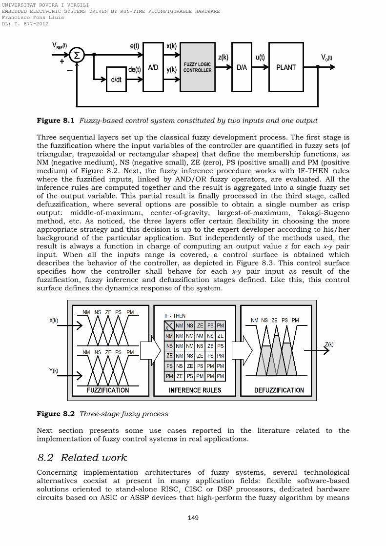
149
Figure 8.1 Fuzzy-based control system constituted by two inputs and one output Three sequential layers set up the classical fuzzy development process. The first stage is the fuzzification where the input variables of the controller are quantified in fuzzy sets (of triangular, trapezoidal or rectangular shapes) that define the membership functions, as NM (negative medium), NS (negative small), ZE (zero), PS (positive small) and PM (positive medium) of Figure 8.2. Next, the fuzzy inference procedure works with IF-THEN rules where the fuzzified inputs, linked by AND/OR fuzzy operators, are evaluated. All the inference rules are computed together and the result is aggregated into a single fuzzy set of the output variable. This partial result is finally processed in the third stage, called defuzzification, where several options are possible to obtain a single number as crisp output: middle-of-maximum, center-of-gravity, largest-of-maximum, Takagi-Sugeno method, etc. As noticed, the three layers offer certain flexibility in choosing the more appropriate strategy and this decision is up to the expert developer according to his/her background of the particular application. But independently of the methods used, the result is always a function in charge of computing an output value z for each x-y pair input. When all the inputs range is covered, a control surface is obtained which describes the behavior of the controller, as depicted in Figure 8.3. This control surface specifies how the controller shall behave for each x-y pair input as result of the fuzzification, fuzzy inference and defuzzification stages defined. Like this, this control surface defines the dynamics response of the system.
Figure 8.2 Three-stage fuzzy process Next section presents some use cases reported in the literature related to the implementation of fuzzy control systems in real applications.
8.2 Related work
Concerning implementation architectures of fuzzy systems, several technological alternatives coexist at present in many application fields: flexible software-based solutions oriented to stand-alone RISC, CISC or DSP processors, dedicated hardware circuits based on ASIC or ASSP devices that high-perform the fuzzy algorithm by means
FUZZY LOGIC
CONTROLLER D/A PLANTA/D
VO(t)
VREF(t)
d/dt
u(t)z(k)
x(k)
y(k)
e(t)
de(t)
Σ+ _ FUZZY LOGIC
CONTROLLER D/A PLANTA/D
VO(t)
VREF(t)
d/dt
u(t)z(k)
x(k)
y(k)
e(t)
de(t)
Σ+ _
UNIVERSITAT ROVIRA I VIRGILI EMBEDDED ELECTRONIC SYSTEMS DRIVEN BY RUN-TIME RECONFIGURABLE HARDWARE Francisco Fons Lluís DL: T. 877-2012
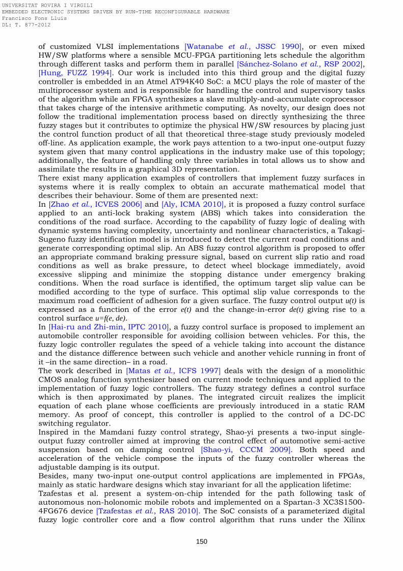
150
of customized VLSI implementations [Watanabe et al., JSSC 1990], or even mixed HW/SW platforms where a sensible MCU-FPGA partitioning lets schedule the algorithm through different tasks and perform them in parallel [Sánchez-Solano et al., RSP 2002], [Hung, FUZZ 1994]. Our work is included into this third group and the digital fuzzy controller is embedded in an Atmel AT94K40 SoC: a MCU plays the role of master of the multiprocessor system and is responsible for handling the control and supervisory tasks of the algorithm while an FPGA synthesizes a slave multiply-and-accumulate coprocessor that takes charge of the intensive arithmetic computing. As novelty, our design does not follow the traditional implementation process based on directly synthesizing the three fuzzy stages but it contributes to optimize the physical HW/SW resources by placing just the control function product of all that theoretical three-stage study previously modeled off-line. As application example, the work pays attention to a two-input one-output fuzzy system given that many control applications in the industry make use of this topology; additionally, the feature of handling only three variables in total allows us to show and assimilate the results in a graphical 3D representation. There exist many application examples of controllers that implement fuzzy surfaces in systems where it is really complex to obtain an accurate mathematical model that describes their behaviour. Some of them are presented next: In [Zhao et al., ICVES 2006] and [Aly, ICMA 2010], it is proposed a fuzzy control surface applied to an anti-lock braking system (ABS) which takes into consideration the conditions of the road surface. According to the capability of fuzzy logic of dealing with dynamic systems having complexity, uncertainty and nonlinear characteristics, a Takagi-Sugeno fuzzy identification model is introduced to detect the current road conditions and generate corresponding optimal slip. An ABS fuzzy control algorithm is proposed to offer an appropriate command braking pressure signal, based on current slip ratio and road conditions as well as brake pressure, to detect wheel blockage immediately, avoid excessive slipping and minimize the stopping distance under emergency braking conditions. When the road surface is identified, the optimum target slip value can be modified according to the type of surface. This optimal slip value corresponds to the maximum road coefficient of adhesion for a given surface. The fuzzy control output u(t) is expressed as a function of the error e(t) and the change-in-error de(t) giving rise to a control surface u=f(e, de). In [Hai-ru and Zhi-min, IPTC 2010], a fuzzy control surface is proposed to implement an automobile controller responsible for avoiding collision between vehicles. For this, the fuzzy logic controller regulates the speed of a vehicle taking into account the distance and the distance difference between such vehicle and another vehicle running in front of it –in the same direction– in a road. The work described in [Matas et al., ICFS 1997] deals with the design of a monolithic CMOS analog function synthesizer based on current mode techniques and applied to the implementation of fuzzy logic controllers. The fuzzy strategy defines a control surface which is then approximated by planes. The integrated circuit realizes the implicit equation of each plane whose coefficients are previously introduced in a static RAM memory. As proof of concept, this controller is applied to the control of a DC-DC switching regulator. Inspired in the Mamdani fuzzy control strategy, Shao-yi presents a two-input single-output fuzzy controller aimed at improving the control effect of automotive semi-active suspension based on damping control [Shao-yi, CCCM 2009]. Both speed and acceleration of the vehicle compose the inputs of the fuzzy controller whereas the adjustable damping is its output. Besides, many two-input one-output control applications are implemented in FPGAs, mainly as static hardware designs which stay invariant for all the application lifetime: Tzafestas et al. present a system-on-chip intended for the path following task of autonomous non-holonomic mobile robots and implemented on a Spartan-3 XC3S1500-4FG676 device [Tzafestas et al., RAS 2010]. The SoC consists of a parameterized digital fuzzy logic controller core and a flow control algorithm that runs under the Xilinx
UNIVERSITAT ROVIRA I VIRGILI EMBEDDED ELECTRONIC SYSTEMS DRIVEN BY RUN-TIME RECONFIGURABLE HARDWARE Francisco Fons Lluís DL: T. 877-2012
151
Microblaze soft-core processor. The FLC plays the role of a co-processor and supports the fuzzy path tracking algorithm. It is connected to the Microblaze via the FSL bus. The placing and routing of the full system occupies 4021 slices, 11 block multipliers and 16 block RAMs. This design achieves a system clock operating frequency of 71 MHz. In [Cortés et al., MICAI 2010], an FPGA implementation of fuzzy system with parametric membership functions and conjunctions is proposed. The implemented system is based on a Sugeno fuzzy model with two input variables. The fuzzy control system is implemented in an Altera Cyclone II EP2C35F672C6. Sánchez-Solano et al. present the hardware/software co-design of a fuzzy control system applied to solving the navigation tasks of an autonomous vehicle [Sánchez-Solano et al., TIE 2007]. The hardware realization of this FLC consumes 3438 slices of the Spartan-xc3s1000 FPGA. The 60% of these resources are required to implement the MicroBlaze processing system and its associated components. The remaining 40% correspond to the fuzzy inference module. The system works at 50 MHz. Once the fuzzy inputs are established, the fuzzy inference module completes the inference process and provides a valid output after 16 clock cycles (320 ns). Although there exist a large amount of FLC designs based on an FPGA or SoC device, very few approaches of fuzzy control systems are implemented in programmable logic platforms that furthermore make use of run-time partial reconfiguration: Mermoud et al. present a fuzzy control system implemented on a Xilinx FPGA platform that is able to evolve at run-time [Mermoud et al., IWANN 2005]. Herein, they concentrate it research in reaching a system architecture able to perform the tuning of system parameters on the fly. In that architecture, parameter tuning implies modifying only some LUT functions. They use the Xilinx difference-based reconfiguration flow since only small modifications are required. With the difference based flow the designer must manually edit low-level changes such as look-up-table equations, internal RAM contents, I/O standards, multiplexers, flip-flop initialization and reset values. Then, a partial bitstream is generated, containing only the differences between the before and the after designs. To this aim, they created three hard macros using LUTs for each evolvable part of the platform: the input membership functions parameters, the inference rules, the aggregation configuration and the output membership functions parameters. By using hard macros location constraints, it is possible to locate each LUT and hence modify it by using difference-based reconfiguration, as described in [Xilinx Inc., XAPP290 2007]. As result, the fuzzy system gets totally defined by an array of bits that configure the different LUTs of the different modules of the fuzzy logic controller. In [Economakos and Economakos, MED 2007], it is proposed a fuzzy logic PID controller where the fuzzy module takes charge of calculating the Kp, Ki and Kd parameters of the PID controller whenever the system is submitted to changes with respect to external conditions. These parameters are then reconfigured at run-time. The system is implemented in a Xilinx Virtex-4 device. The fuzzy logic module is implemented in software by means of an embedded soft-core host processor while the PID controller is implemented in hardware. The host processor –MicroBlaze soft-core instance– calculates the fuzzy gain parameters for PID control and also generates all reconfiguration information to perform parameter changes. The PID parameters are stored in a single reconfiguration frame of the FPGA; this constrained placement is intended to reduce the reconfiguration time to a minimum, in accordance with the reconfiguration grain of the Virtex-4 device. The reconfiguration is performed through the ICAP interface by means of the HWICAP controller and managed by MicroBlaze. When the fuzzy logic module calculates new values for the PID parameters, these can be written directly to the appropriate place within the reconfiguration frame and then be exchanged in the FPGA configuration memory through HWICAP. The main advantage of this approach is that by reconfiguring small parts of the application (only the PID parameters) the reconfiguration does not impose time overheads that make online reconfiguration not practical. The FLC proposed in this chapter keeps some similarities with some of these works regarding the use of run-time partial reconfiguration.
UNIVERSITAT ROVIRA I VIRGILI EMBEDDED ELECTRONIC SYSTEMS DRIVEN BY RUN-TIME RECONFIGURABLE HARDWARE Francisco Fons Lluís DL: T. 877-2012
152
8.3 Hardware/Software co-design
Getting the support of simulation tools is a habitual practice in the development of fuzzy control systems; Matlab-Simulink, for instance, offers a toolbox that permits one to perform all the fuzzy logic stages. Once the controller is modelled with the help of these tools, the physical implementation of the three-stage algorithm can be carried out in software and/or hardware. Many research efforts have been addressed to find strategies able to optimize the implementation and accelerate the processing. In the particular case of two-input one-ouput control systems, instead of going through the specific hardware or software implementation of the fuzzifier, rules-based inference engine and defuzzifier the work presented in this chapter proposes a new approach focused on directly implementing the resultant fuzzy control surface z=f(x,y). Hence, this approach does not demand a concrete fuzzification or defuzzification method since it takes as input just the resultant control surface coming from the theoretical fuzzy model. This feature adds flexibility to the design, without loosing generality, in search of a universality-oriented FLC. The proposed controller is then deployed through HW/SW tasks partitioning in the Atmel AT94K40 FPSLIC: the CPU manages the application flow in software while a hardware coprocessor mapped in the FPGA takes charge of the fuzzy control surface computation. Following it is described how this system is synthesized in programmable logic aimed at computing the z=f(x,y) function in a cost- and time-efficient way.
8.3.1 Fuzzy algorithm
Nonlinear surfaces result when designing a two-inputs one-output FLC for controlling a nonlinear system. An option for implementing this 2D function would be to directly store the control surface point-by-point into a LUT but this approach would require an intolerable amount of memory in most cases [Dharia et al., IJCNN 2002]. Our challenge then is to split the control surface z=f(x,y) in a set of n rectangular areas and model each of them through a second-order function through multiple polynomial regression, that is,
22),( yfxeyxdycxbayxfz ⋅+⋅+⋅⋅+⋅+⋅+== (8.1)
where the surface of each rectangular sector, limited by its two extreme up-left and down-right vertexes (xul,yul) and (xdr,ydr), yul ≤ y ≤ ydr, xul ≤ x ≤ xdr, becomes totally defined by 6 coefficients a, b, c, d, e, f . The key point of this approach is to find the convenient n rectangles in which the surface should be split in order to reach the modeling of the partial surfaces as similar to the original fuzzy control surface as possible, within an acceptable error ε. Mathematical-statistical software tools can assist this development task, e.g. Minitab. The number of rectangles n and their sizes, i.e. (x0,x1,…xi), (y0, y1,…yj) partitions, are a function of the control surface, which obviously depends, in the last term, on the features of the whole plant-controller, as depicted in Figure 8.1. The partitioning of the surface into rectangular parts shall make feasible its subsequent storage and indexing in memory (2D-coordinates and polynomial coefficients). In fact, the resultant n rectangular sectors that comprise the whole control surface are indexed and stored in increasing order into SRAM –as a function of the Y and X components of their extreme vertexes, and considering the component Y of higher weight than the component X– as illustrated in Figure 8.3. Moreover, this flexibility in segmenting the surface permits to cover not only continuous surfaces but also discontinuous ones typical of nonlinear systems (saturation effects, etc). All this conditioning must enable later to use a binary search algorithm to find in real-time at which sector falls each periodic sampling point (xp,yp). Besides, it is important to note in this approach that, until now, both fuzzy development process and surface polynomial modeling are tasks carried out off-line; in fact, they constitute the theoretical analysis/study previous to the system implementation, and the fact of skipping all this fuzzy preprocessing in the implementation aims to simplify the HW/SW design as well as reduce costs.
UNIVERSITAT ROVIRA I VIRGILI EMBEDDED ELECTRONIC SYSTEMS DRIVEN BY RUN-TIME RECONFIGURABLE HARDWARE Francisco Fons Lluís DL: T. 877-2012
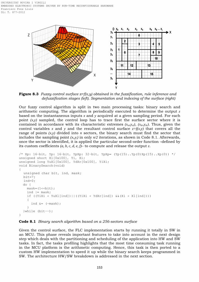
153
Y
X0 x0 x1 x2 x3 x4 x5 x6 ... xj
y00
1
23 4 5
67
8 9
10
11 12 13
14 15
y1
y2
y3
y4
y5
y6
yk
...
Z
XY
Y
X0 x0 x1 x2 x3 x4 x5 x6 ... xj
y00
1
23 4 5
67
8 9
10
11 12 13
14 15
y1
y2
y3
y4
y5
y6
yk
...
Y
X0 x0 x1 x2 x3 x4 x5 x6 ... xj
y00
1
23 4 5
67
8 9
10
11 12 13
14 15
y1
y2
y3
y4
y5
y6
yk
...
Z
XY
Z
XY
Figure 8.3 Fuzzy control surface z=f(x,y) obtained in the fuzzification, rule inference and
defuzzification stages (left). Segmentation and indexing of the surface (right) Our fuzzy control algorithm is split in two main processing tasks: binary search and arithmetic computing. The algorithm is periodically executed to determine the output z based on the instantaneous inputs x and y acquired at a given sampling period. For each point (x,y) sampled, the control loop has to trace first the surface sector where it is contained in accordance with its characteristic extremes (xul,yul), (xdr,ydr). Thus, given the control variables x and y and the resultant control surface z=f(x,y) that covers all the range of points (x,y) divided into n sectors, the binary search must find the sector that includes the sampling point (xi,yi) in only n/2 iterations, as shown in Code 8.1. Afterwards, once the sector is identified, it is applied the particular second-order function –defined by its custom coefficients (a, b, c, d, e, f)– to compute and release the output z. /* Xp: 16-bit, Yp: 16-bit, YpXp: 32-bit, YpXp= (Yp(15)..Yp(0)Xp(15)..Xp(0)) */ unsigned short Xl[0x100], Yi, Xi; unsigned long YuXl[0x100], YdXr[0x100], YiXi; void BinarySearch(void)
unsigned char bit, ind, mask; bit=7; ind=0;
do mask=(1<<bit); ind |= mask; if ((YiXi < YuXl[ind])||((YiXi < YdXr[ind]) &&(Xi < Xl[ind]))) ind &= (~mask); while (bit--);
Code 8.1 Binary search algorithm based on a 256-sectors surface Given the control surface, the FLC implementation starts by running it totally in SW in an MCU. This phase reveals important features to take into account in the next design step which deals with the partitioning and scheduling of the application into HW and SW tasks. In fact, the tasks profiling highlights that the most time consuming task running in the MCU platform is the arithmetic computing. Hence, this task is then ported to a custom HW implementation to speed it up while the binary search keeps programmed in SW. The architecture HW/SW breakdown is addressed in the next section.
UNIVERSITAT ROVIRA I VIRGILI EMBEDDED ELECTRONIC SYSTEMS DRIVEN BY RUN-TIME RECONFIGURABLE HARDWARE Francisco Fons Lluís DL: T. 877-2012
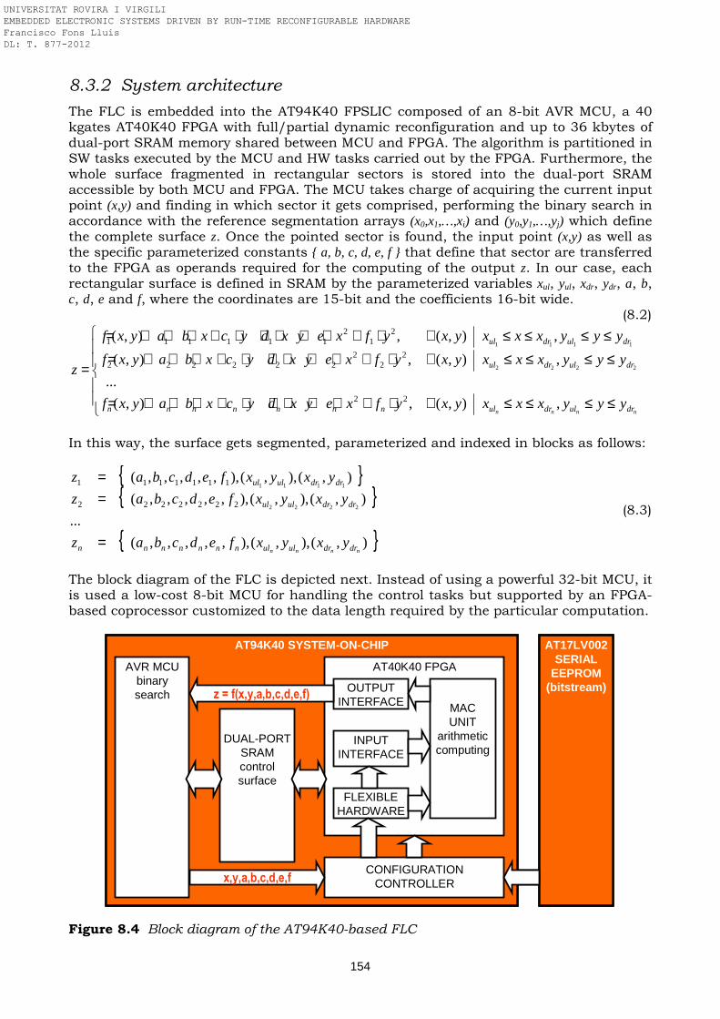
154
8.3.2 System architecture
The FLC is embedded into the AT94K40 FPSLIC composed of an 8-bit AVR MCU, a 40 kgates AT40K40 FPGA with full/partial dynamic reconfiguration and up to 36 kbytes of dual-port SRAM memory shared between MCU and FPGA. The algorithm is partitioned in SW tasks executed by the MCU and HW tasks carried out by the FPGA. Furthermore, the whole surface fragmented in rectangular sectors is stored into the dual-port SRAM accessible by both MCU and FPGA. The MCU takes charge of acquiring the current input point (x,y) and finding in which sector it gets comprised, performing the binary search in accordance with the reference segmentation arrays (x0,x1,…,xi) and (y0,y1,…,yj) which define the complete surface z. Once the pointed sector is found, the input point (x,y) as well as the specific parameterized constants a, b, c, d, e, f that define that sector are transferred to the FPGA as operands required for the computing of the output z. In our case, each rectangular surface is defined in SRAM by the parameterized variables xul, yul, xdr, ydr, a, b, c, d, e and f, where the coordinates are 15-bit and the coefficients 16-bit wide. (8.2)
≤≤≤≤∀⋅+⋅+⋅⋅+⋅+⋅+=
≤≤≤≤∀⋅+⋅+⋅⋅+⋅+⋅+=≤≤≤≤∀⋅+⋅+⋅⋅+⋅+⋅+=
=
nnnn druldrulnnnnnnn
druldrul
druldrul
yyyxxxyxyfxeyxdycxbayxf
yyyxxxyxyfxeyxdycxbayxf
yyyxxxyxyfxeyxdycxbayxf
z
,),(,),(
...
,),(,),(
,),(,),(
22
22
2222222
21
2111111
2222
1111
In this way, the surface gets segmented, parameterized and indexed in blocks as follows:
),(),,(),,,,,,(
...
),(),,(),,,,,,(
),(),,(),,,,,,(
2222
1111
2222222
1111111
nnnn drdrululnnnnnnn
drdrulul
drdrulul
yxyxfedcbaz
yxyxfedcbaz
yxyxfedcbaz
=
==
(8.3)
The block diagram of the FLC is depicted next. Instead of using a powerful 32-bit MCU, it is used a low-cost 8-bit MCU for handling the control tasks but supported by an FPGA-based coprocessor customized to the data length required by the particular computation.
Figure 8.4 Block diagram of the AT94K40-based FLC
AT94K40 SYSTEM-ON-CHIP
AT40K40 FPGAAVR MCUbinarysearch
AT17LV002SERIAL
EEPROM(bitstream)
MACUNIT
arithmeticcomputing
INPUTINTERFACE
OUTPUTINTERFACE
FLEXIBLEHARDWARE
CONFIGURATIONCONTROLLER
DUAL-PORTSRAMcontrolsurface
AT94K40 SYSTEM-ON-CHIP
AT40K40 FPGAAVR MCUbinarysearch
AT17LV002SERIAL
EEPROM(bitstream)
MACUNIT
arithmeticcomputing
INPUTINTERFACE
OUTPUTINTERFACE
FLEXIBLEHARDWARE
CONFIGURATIONCONTROLLER
DUAL-PORTSRAMcontrolsurface
x,y,a,b,c,d,e,f
z = f(x,y,a,b,c,d,e,f)
UNIVERSITAT ROVIRA I VIRGILI EMBEDDED ELECTRONIC SYSTEMS DRIVEN BY RUN-TIME RECONFIGURABLE HARDWARE Francisco Fons Lluís DL: T. 877-2012
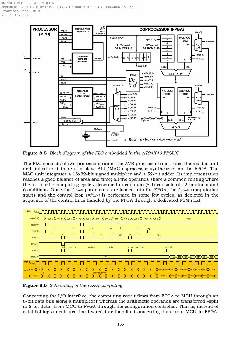
155
Figure 8.5 Block diagram of the FLC embedded in the AT94K40 FPSLIC The FLC consists of two processing units: the AVR processor constitutes the master unit and linked to it there is a slave ALU/MAC coprocessor synthesized on the FPGA. The MAC unit integrates a 16x32-bit signed multiplier and a 52-bit adder. Its implementation reaches a good balance of area and time; all the operands share a common routing where the arithmetic computing cycle z described in equation (8.1) consists of 12 products and 6 additions. Once the fuzzy parameters are loaded into the FPGA, the fuzzy computation starts and the control loop z=f(x,y) is performed in some few cycles, as depicted in the sequence of the control lines handled by the FPGA through a dedicated FSM next.
Figure 8.6 Scheduling of the fuzzy computing Concerning the I/O interface, the computing result flows from FPGA to MCU through an 8-bit data bus along a multiplexer whereas the arithmetic operands are transferred –split in 8-bit data– from MCU to FPGA through the configuration controller. That is, instead of establishing a dedicated hard-wired interface for transferring data from MCU to FPGA,
di
AT17LV002EEPROM
(bitstream)
PROCESSOR(MCU)
COPROCESSOR (FPGA)FPGAX
FPGAY
FPGAZ
FPGAD
8-bit OUTPUT
CS
CLKAVR
CONFIGURATIONCONTROLLER
FSM
CLKAT40K
FREQ.DIVIDER
fCLK/2 zi = f(xi,yi) = ai + bixi + ciyi + dixiyi + eixi2 + fiyi
2
DUAL-PORTSRAM
(control surface)
MUL 16x32
ai
bi
ci
ei
fi
00000001
WR EN
PWMZi
PORT D
PORT EYi
Xi
q(47)&q(47) &q(47)&q(47) &q(47..0)
LUT-basedDR-ROM 8x16
DATA OUT
ADDRESS
WR EN
ADDRESS
RD EN
WR EN
DATA
CLKAVR CLKAT40K
8-bitDATA24-bit
ADDRESS
16-bit
DATA IN
IOWE
INIT
CON
SDATA
CCLK
yi
xi
32-bit
MULACCffD32
PRODUCTffD48
ADDACCffD52
ADD 52
52-bit 52-bit
MUX2x8
MUX8x8
LUT-basedDR-MIXER 8x8
IORE
enfsm(2..0)
ldfsm(1..0)
rdfsm(2..0)
zi (07..00)
zi (15..08)
zi (23..16)
zi (31..24)
zi (39..32)
zi (47..40)
zi (55..48)
swap(7..0)
opfsm(2..0)
rdfsm(2..0)
opfsm(2..0)
CLKAT40K
D
Q
ldfsm(0)
MUX2x52
CLKAT40KCLKAT40K
DD
ldfsm(1)
enfsm(0)
enfsm(1)enfsm(2)
addacc(51..0),zi (51..0)
000...000
selfsm(2..0)
selfsm(2..0)
swap(7..0)
8-bit DR-INPUT
yi xi ai bi ci di ei fi
ch7
ch0
di
AT17LV002EEPROM
(bitstream)
PROCESSOR(MCU)
COPROCESSOR (FPGA)FPGAX
FPGAY
FPGAZ
FPGAD
8-bit OUTPUT
CS
CLKAVR
CONFIGURATIONCONTROLLER
FSM
CLKAT40K
FREQ.DIVIDER
fCLK/2 zi = f(xi,yi) = ai + bixi + ciyi + dixiyi + eixi2 + fiyi
2
DUAL-PORTSRAM
(control surface)
MUL 16x32
ai
bi
ci
ei
fi
00000001
WR EN
PWMZi
PORT D
PORT EYi
Xi
q(47)&q(47) &q(47)&q(47) &q(47..0)q(47)&q(47) &q(47)&q(47) &q(47..0)
LUT-basedDR-ROM 8x16
DATA OUT
ADDRESS
WR EN
ADDRESS
RD EN
WR EN
DATA
CLKAVR CLKAT40K
8-bitDATA24-bit
ADDRESS
16-bit
DATA IN
IOWE
INIT
CON
SDATA
CCLK
yi
xi
32-bit
MULACCffD32
PRODUCTffD48
ADDACCffD52
ADD 52
52-bit 52-bit
MUX2x8
MUX8x8
LUT-basedDR-MIXER 8x8
IORE
enfsm(2..0)
ldfsm(1..0)
rdfsm(2..0)
zi (07..00)
zi (15..08)
zi (23..16)
zi (31..24)
zi (39..32)
zi (47..40)
zi (55..48)
swap(7..0)
opfsm(2..0)
rdfsm(2..0)
opfsm(2..0)
CLKAT40K
D
Q
ldfsm(0)
MUX2x52
CLKAT40KCLKAT40K
DD
ldfsm(1)
enfsm(0)
enfsm(1)enfsm(2)
addacc(51..0),zi (51..0)addacc(51..0),zi (51..0)
000...000
selfsm(2..0)
selfsm(2..0)
swap(7..0)
8-bit DR-INPUT
yi xi ai bi ci di ei fi
ch7
ch0
FPGA
MCU
opfsm(2..0)
clkAVR
in R, @ in R, @ in R, @ in R, @ in R, @ in R, @ in R, @
application code
out @, RASM
b6=fisucfisua=0C
b4=fisuc b3=fisuc b2=fisuc b1=fisuc b0=fisuc
ldi R, 0 out @, R
fisub=0
ldi R, 0
b5=fisuc
001-x 011-b 001-x 110-e 000-y 100-c 000-y 111-f 010-a 001-x 000-y 101-d 000-y
110 101 100 011 010 001 000111
clkAT40K
ldsfsm(0)
enfsm(0)
enfsm(2)
ldsfsm(1)
enfsm(1)
1 1x xx 1 1y yy 1 1x xy
xyd1ayyfycxxexb
z=z+xbz=0 z=z+xxe z=z+yc z=z+yyf z=z+1a z=z+xyd
rdfsm(2..0)
UNIVERSITAT ROVIRA I VIRGILI EMBEDDED ELECTRONIC SYSTEMS DRIVEN BY RUN-TIME RECONFIGURABLE HARDWARE Francisco Fons Lluís DL: T. 877-2012
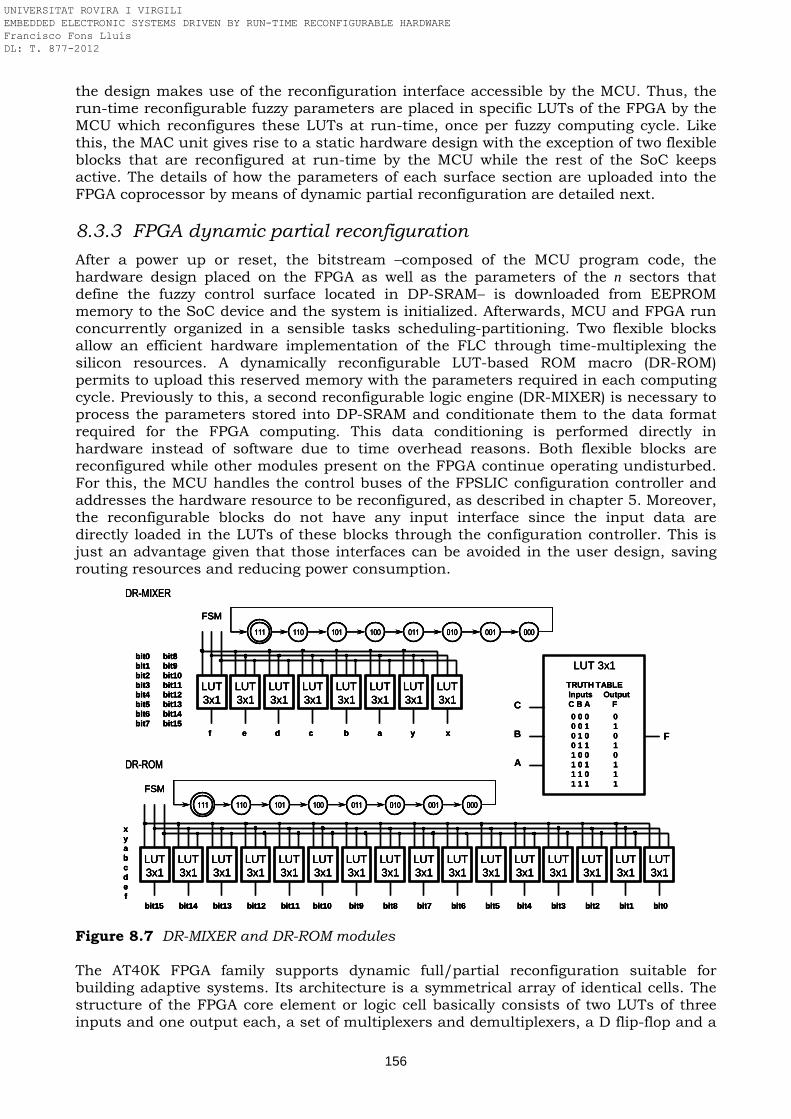
156
the design makes use of the reconfiguration interface accessible by the MCU. Thus, the run-time reconfigurable fuzzy parameters are placed in specific LUTs of the FPGA by the MCU which reconfigures these LUTs at run-time, once per fuzzy computing cycle. Like this, the MAC unit gives rise to a static hardware design with the exception of two flexible blocks that are reconfigured at run-time by the MCU while the rest of the SoC keeps active. The details of how the parameters of each surface section are uploaded into the FPGA coprocessor by means of dynamic partial reconfiguration are detailed next.
8.3.3 FPGA dynamic partial reconfiguration
After a power up or reset, the bitstream –composed of the MCU program code, the hardware design placed on the FPGA as well as the parameters of the n sectors that define the fuzzy control surface located in DP-SRAM– is downloaded from EEPROM memory to the SoC device and the system is initialized. Afterwards, MCU and FPGA run concurrently organized in a sensible tasks scheduling-partitioning. Two flexible blocks allow an efficient hardware implementation of the FLC through time-multiplexing the silicon resources. A dynamically reconfigurable LUT-based ROM macro (DR-ROM) permits to upload this reserved memory with the parameters required in each computing cycle. Previously to this, a second reconfigurable logic engine (DR-MIXER) is necessary to process the parameters stored into DP-SRAM and conditionate them to the data format required for the FPGA computing. This data conditioning is performed directly in hardware instead of software due to time overhead reasons. Both flexible blocks are reconfigured while other modules present on the FPGA continue operating undisturbed. For this, the MCU handles the control buses of the FPSLIC configuration controller and addresses the hardware resource to be reconfigured, as described in chapter 5. Moreover, the reconfigurable blocks do not have any input interface since the input data are directly loaded in the LUTs of these blocks through the configuration controller. This is just an advantage given that those interfaces can be avoided in the user design, saving routing resources and reducing power consumption.
DR-MIXER
xyabcdef
LUT3x1
LUT3x1
LUT3x1
LUT3x1
LUT3x1
LUT3x1
LUT3x1
LUT3x1
LUT3x1
LUT3x1
LUT3x1
LUT3x1
LUT3x1
LUT3x1
LUT3x1
LUT3x1
bit15 bit14 bit13 bit12 bit11 bit10 bit9 bit8 bit7 bit6 bit5 bit4 bit3 bit2 bit1 bit0
FSM
111 110 101 100 011 010 001 000
bit0 bit8bit1 bit9 bit2 bit10bit3 bit11bit4 bit12bit5 bit13bit6 bit14bit7 bit15
LUT3x1
LUT3x1
LUT3x1
LUT3x1
LUT3x1
LUT3x1
LUT3x1
LUT3x1
f e d c b a y x
FSM
111 110 101 100 011 010 001 000
DR-ROM
TRUTH TABLEInputs OutputC B A F
0 0 0 00 0 1 10 1 0 00 1 1 11 0 0 01 0 1 11 1 0 11 1 1 1
LUT 3x1
F
C
B
A
DR-MIXER
xyabcdef
LUT3x1
LUT3x1
LUT3x1
LUT3x1
LUT3x1
LUT3x1
LUT3x1
LUT3x1
LUT3x1
LUT3x1
LUT3x1
LUT3x1
LUT3x1
LUT3x1
LUT3x1
LUT3x1
bit15 bit14 bit13 bit12 bit11 bit10 bit9 bit8 bit7 bit6 bit5 bit4 bit3 bit2 bit1 bit0
FSM
111 110 101 100 011 010 001 000
bit0 bit8bit1 bit9 bit2 bit10bit3 bit11bit4 bit12bit5 bit13bit6 bit14bit7 bit15
LUT3x1
LUT3x1
LUT3x1
LUT3x1
LUT3x1
LUT3x1
LUT3x1
LUT3x1
f e d c b a y x
FSM
111 110 101 100 011 010 001 000
DR-ROM
DR-MIXER
xyabcdef
LUT3x1
LUT3x1
LUT3x1
LUT3x1
LUT3x1
LUT3x1
LUT3x1
LUT3x1
LUT3x1
LUT3x1
LUT3x1
LUT3x1
LUT3x1
LUT3x1
LUT3x1
LUT3x1
bit15 bit14 bit13 bit12 bit11 bit10 bit9 bit8 bit7 bit6 bit5 bit4 bit3 bit2 bit1 bit0
FSM
111 110 101 100 011 010 001 000
xyabcdef
LUT3x1
LUT3x1
LUT3x1
LUT3x1
LUT3x1
LUT3x1
LUT3x1
LUT3x1
LUT3x1
LUT3x1
LUT3x1
LUT3x1
LUT3x1
LUT3x1
LUT3x1
LUT3x1
bit15 bit14 bit13 bit12 bit11 bit10 bit9 bit8 bit7 bit6 bit5 bit4 bit3 bit2 bit1 bit0
FSM
111 110 101 100 011 010 001 000
bit0 bit8bit1 bit9 bit2 bit10bit3 bit11bit4 bit12bit5 bit13bit6 bit14bit7 bit15
LUT3x1
LUT3x1
LUT3x1
LUT3x1
LUT3x1
LUT3x1
LUT3x1
LUT3x1
f e d c b a y x
FSM
111 110 101 100 011 010 001 000
bit0 bit8bit1 bit9 bit2 bit10bit3 bit11bit4 bit12bit5 bit13bit6 bit14bit7 bit15
LUT3x1
LUT3x1
LUT3x1
LUT3x1
LUT3x1
LUT3x1
LUT3x1
LUT3x1
f e d c b a y x
FSM
111 110 101 100 011 010 001 000
DR-ROM
TRUTH TABLEInputs OutputC B A F
0 0 0 00 0 1 10 1 0 00 1 1 11 0 0 01 0 1 11 1 0 11 1 1 1
LUT 3x1
F
C
B
A
TRUTH TABLEInputs OutputC B A F
0 0 0 00 0 1 10 1 0 00 1 1 11 0 0 01 0 1 11 1 0 11 1 1 1
LUT 3x1
F
C
B
A
Figure 8.7 DR-MIXER and DR-ROM modules The AT40K FPGA family supports dynamic full/partial reconfiguration suitable for building adaptive systems. Its architecture is a symmetrical array of identical cells. The structure of the FPGA core element or logic cell basically consists of two LUTs of three inputs and one output each, a set of multiplexers and demultiplexers, a D flip-flop and a
UNIVERSITAT ROVIRA I VIRGILI EMBEDDED ELECTRONIC SYSTEMS DRIVEN BY RUN-TIME RECONFIGURABLE HARDWARE Francisco Fons Lluís DL: T. 877-2012
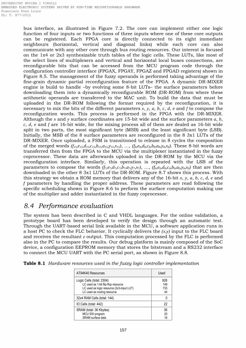
157
bus interface, as illustrated in Figure 7.2. The core can implement either one logic function of four inputs or two functions of three inputs where one of these core outputs can be registered. Each FPGA core is directly connected to its eight immediate neighbours (horizontal, vertical and diagonal links) while each core can also communicate with any other core through bus routing resources. Our interest is focused on the 1x4 or 2x3 synthesizable truth tables of the logic cells. These LUTs, like most of the select lines of multiplexers and vertical and horizontal local buses connections, are reconfigurable bits that can be accessed from the MCU program code through the configuration controller interface (FPGAX, FPGAY, FPGAZ and FPGAD registers) shown in Figure 8.5. The management of the fuzzy operands is performed taking advantage of the fine-grain dynamic partial reconfiguration feature of the FPGA. A dynamic DR-MIXER engine is build to handle –by evolving some 8-bit LUTs– the surface parameters before downloading them into a dynamically reconfigurable ROM (DR-ROM) from where these arithmetic operands are transferred to the MAC unit. To build the data that must be uploaded in the DR-ROM following the format required by the reconfiguration, it is necessary to mix the bits of the different parameters x, y, a, b, c, d, e and f to compose the reconfiguration words. This process is performed in the FPGA with the DR-MIXER. Although the x and y surface coordinates are 15-bit wide and the surface parameters a, b, c, d, e and f are 16-bit wide, for the mixing process all of them are dealed as 16-bit wide split in two parts, the most significant byte (MSB) and the least significant byte (LSB). Initially, the MSB of the 8 surface parameters are reconfigured in the 8 3x1 LUTs of the DR-MIXER. Once uploaded, a FSM is transitioned to release in 8 cycles the composition of the merged words (f15,e15,d15,c15,b15,a15,y15,x15), …, (f8,e8,d8,c8,b8,a8,y8,x8). These 8-bit words are transferred then from the FPGA to the MCU via the multiplexer instantiated in the fuzzy coprocessor. These data are afterwards uploaded in the DR-ROM by the MCU via the reconfiguration interface. Similarly, this operation is repeated with the LSB of the parameters to compose the words (f7,e7,d7,c7,b7,a7,y7,x7), …, (f0,e0,d0,c0,b0,a0,y0,x0) that are then downloaded in the other 8 3x1 LUTs of the DR-ROM. Figure 8.7 shows this process. With this strategy we obtain a ROM memory that delivers any of the 16-bit x, y, a, b, c, d, e and f parameters by handling the proper address. These parameters are read following the specific scheduling shown in Figure 8.6 to perform the surface computation making use of the multiplier and adder instantiated in the fuzzy coprocessor.
8.4 Performance evaluation
The system has been described in C and VHDL languages. For the online validation, a prototype board has been developed to verify the design through an automatic test. Through the UART-based serial link available in the MCU, a software application runs in a host PC to check the FLC behavior. It cyclically delivers the (x,y) input to the FLC board and receives the resultant z output. This computation processed by the FLC is performed also in the PC to compare the results. Our debug platform is mainly composed of the SoC device, a configuration EEPROM memory that stores the bitstream and a RS232 interface to connect the MCU UART with the PC serial port, as shown in Figure 8.8. Table 8.1 Hardware resources used in the fuzzy logic controller implementation
AT94K40 Resources Used
Logic Cells (total: 2304) LC used as 1-bit flip-flop resource LC used as logic resource (2x3-input LUT) LC used as routing resource
926 149 733
44
32x4 RAM Cells (total: 144) 0
IO Cells (total: 442) 22
SRAM (total: 36 Kbytes) MCU SW program SRAM surface data
36 20 16
UNIVERSITAT ROVIRA I VIRGILI EMBEDDED ELECTRONIC SYSTEMS DRIVEN BY RUN-TIME RECONFIGURABLE HARDWARE Francisco Fons Lluís DL: T. 877-2012
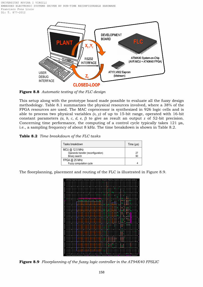
158
Figure 8.8 Automatic testing of the FLC design This setup along with the prototype board made possible to evaluate all the fuzzy design methodology. Table 8.1 summarizes the physical resources involved, where a 38% of the FPGA resources are used. The MAC coprocessor is synthesized in 926 logic cells and is able to process two physical variables (x, y) of up to 15-bit range, operated with 16-bit constant parameters (a, b, c, d, e, f) to give as result an output z of 52-bit precision. Concerning time performance, the computing of a control cycle typically takes 121 µs, i.e., a sampling frequency of about 8 kHz. The time breakdown is shown in Table 8.2. Table 8.2 Time breakdown of the FLC tasks
Tasks breakdown Time (µs)
MCU @ 12.5 MHz Operands transfer (reconfiguration) Binary search
27 90
FPGA @ 25 MHz Fuzzy computation cycle
4
The floorplanning, placement and routing of the FLC is illustrated in Figure 8.9.
Figure 8.9 Floorplanning of the fuzzy logic controller in the AT94K40 FPSLIC
USERDEBUGINTERFACE
RS232INTERFACE
DEVELOPMENTBOARD
AT17LV002 Eeprom(bitstream)
AT94K40 System-on-Chip(AVR MCU + AT40K40 FPGA)
Xi ,Yi
Zi
CLOSED-LOOP
PLANT FLC
USERDEBUGINTERFACE
RS232INTERFACE
DEVELOPMENTBOARD
AT17LV002 Eeprom(bitstream)
AT94K40 System-on-Chip(AVR MCU + AT40K40 FPGA)
Xi ,Yi
Zi
CLOSED-LOOP
PLANT FLC
UNIVERSITAT ROVIRA I VIRGILI EMBEDDED ELECTRONIC SYSTEMS DRIVEN BY RUN-TIME RECONFIGURABLE HARDWARE Francisco Fons Lluís DL: T. 877-2012
159
8.5 Summary
In the research field of control systems, the development of decision strategies necessary for autonomous operation plays a central role. Many studies focus on behavior-based approaches, in which the reactivity to unforeseeable circumstances is achieved with computationally simple algorithms that process sensory information in real-time by means of high-level inference mechanisms. In this context, fuzzy logic is often adopted to overcome the difficulties of modeling the unstructured, dynamically changing environment which is difficult to express using mathematical equations. Fuzzy control becomes a practical alternative for the design of a great variety of control applications. It provides an advisable method for the synthesis of non-linear controllers using heuristic information. The relatively simple architecture of the FLC processing algorithm naturally leads to straightforward implementations in dedicated hardware instead of software-based approaches. In fact, its execution on an instruction-set processor is often too slow. FPGAs, on the other hand, deliver true parallel execution and make possible to exceed the computing power of processors executing programs just by breaking the paradigm of sequential execution and accomplishing more per clock cycle. Flexibility is another of the strong points of these control systems; this feature is accentuated in run-time partially reconfigurable FPGAs by allowing hardware to be adjusted on-demand. This work presents a novel methodology for developing two-input one-output fuzzy controllers taking into account the fact that a clear trade-off shall be met between the accuracy of the computing results and the implementation costs. The commercial success or failure of this product will highly depend on this compromise. In this direction, the design flow is conceptually split in two basic stages: a first phase of intensive study performed off-line which includes the traditional three-stage fuzzy system simulation followed by a multiple polynomial regression of the output function, and a second phase where this resultant mathematic model is implemented through HW/SW co-design in search of a cost-effective and generic solution that lets reduce the fuzzy computing to a simple binary search process followed by a multiply-and-accumulate arithmetic operation. As application example, a general-purpose dual-input single-output FLC has been embedded in a SoC suitable for whichever industrial application: by only changing the RAM data of the control surface it can switch from one application to another, converting this approach into a universal and field-customizable solution. The parameterized surface information is included into the bitstream as a simple data file with the rectangular sectors composed of their border coordinates and function polynomial coefficients. These data are swapped in the coprocessor by exploiting fine-grain partial reconfiguration. As summary, this chapter shows an application example of the embedded CPU+FPGA system architecture proposed in this dissertation. A simple run-time reconfigurable hardware arithmetic coprocessor attached to a small 8-bit MCU –all integrated in a SoC device– is a valid alternative in terms of performance-cost to a purely software solution based on a more powerful (32-bit) MCU to take charge of the real-time FLC computation. Besides, this work demonstrates the feasibility of use of reconfigurable computing in the industry.
References
[Aly, ICMA 2010] A.A. Aly, Intelligent fuzzy control for antilock brake system with road-surfaces identifier, Proceedings of the International Conference on Mechatronics and Automation, pp. 699-705, 2010.
[Cortés et al., MICAI 2010] P. Cortés Antonio, I. Batyrshin, H. Molina Lozano, L.A. Villa Vargas, I. Rudas, FPGA implementation of fuzzy system with parametric membership functions and parametric conjunctions, Proc. of the Mexican International Conference on Artificial Intelligence, LNCS, vol. 6438, pp. 487–499, Springer, 2010.
[Dharia et al., IJCNN 2002] N. Dharia, J. Gownipalli, O. Kaynak, B.M. Wilamowski, Fuzzy controller with second order defuzzification algorithm, Proc. of the Int. Joint Conference on Neural Networks, vol. 3, pp. 2327-2332, 2002.
UNIVERSITAT ROVIRA I VIRGILI EMBEDDED ELECTRONIC SYSTEMS DRIVEN BY RUN-TIME RECONFIGURABLE HARDWARE Francisco Fons Lluís DL: T. 877-2012
160
[Economakos and Economakos, MED 2007] G. Economakos, C. Economakos, A run-time reconfigurable fuzzy PID controller based on modern FPGA devices, Proceedings of the Mediterranean Conference on Control and Automation, pp. 1-6, 2007.
[Hai-ru and Zhi-min, IPTC 2010] G. Hai-ru, L. Zhi-min, An intelligent controller design for automobile anti-collision based on fuzzy network, Proc. Int. Symposium on Intelligence Information Processing and Trusted Computing, pp. 305-308, 2010.
[Hung, FUZZ 1994] D.L. Hung, Custom design of a hardware fuzzy logic controller, Proceedings of the IEEE Conference on Fuzzy Systems, vol. 3, pp. 1781-1785, 1994.
[Matas et al., ICFS 1997] J. Matas, L. García de Vicuña, M. Castilla, A synthesys of fuzzy control surfaces in CMOS technology, Proceedings of the IEEE International Conference on Fuzzy Systems, vol. 2, pp. 641-646, 1997.
[Mermoud et al., IWANN 2005] G. Mermoud, A. Upegui, C.A. Peña, E. Sanchez, A dynamically-reconfigurable FPGA platform for evolving fuzzy systems, Proc. of the Int. Work-Conference on Artificial Neural Network, LNCS, vol. 3512, pp. 572–581, Springer, 2005.
[Sánchez-Solano et al., RSP 2002] S. Sánchez-Solano, R. Senhadji, A. Cabrera, I. Baturone, C.J. Jiménez, A. Barriga, Prototyping of fuzzy logic-based controllers using standard FPGA development boards, Proceedings of the IEEE International Workshop on Rapid System Prototyping, pp. 25-32, 2002.
[Sánchez-Solano et al., TIE 2007] S. Sánchez-Solano, A.J. Cabrera, I. Baturone, F.J. Moreno-Velo, M. Brox, FPGA implementation of embedded fuzzy controllers for robotic applications, IEEE Transactions on Industrial Electronics, vol. 54, no. 4, pp. 1937-1945, 2007.
[Shao-yi, CCCM 2009] B. Shao-yi, Fuzzy controller for automotive semi-active suspension based on damping control, Proc. of the ISECS Int. Colloquium on Computing, Communication, Control, and Management, pp.296-299, 2009.
[Togai and Watanabe, Expert 1986] M. Togai, H. Watanabe, Expert system on a chip: an engine for real-time approximate reasoning, IEEE Expert Magazine, vol. 1, no. 3, pp. 55–62, 1986.
[Tzafestas et al., RAS 2010] S.G. Tzafestas, K.M. Deliparaschos, G.P. Moustri, Fuzzy logic path tracking control for autonomous non-holonomic mobile robots: design of system on a chip, Robotics and Autonomous Systems, vol. 58, pp. 1017-1027, 2010.
[Watanabe et al., JSSC 1990] H. Watanabe, W.D. Dettloff, K.E. Yount, A VLSI fuzzy logic controller with reconfigurable, cascadable architecture, IEEE Journal of Solid-State Circuits, vol. 25, no. 2, pp. 376-382, 1990.
[Xilinx Inc., XAPP290 2007] E. Eto, Difference-based partial reconfiguration, Xilinx Inc, Application Note XAPP290 (v2.0), 2007.
[Yamakawa and Miki, TC 1986] T. Yamakawa, T. Miki, The current mode fuzzy logic integrated circuits fabricated by the standard CMOS process, IEEE Transactions on Computers, vol. 35, no. 2, pp. 161–167, 1986.
[Zadeh, IC 1965] L.A. Zadeh, Fuzzy Sets, Information and Control, vol. 8, no. 3, pp. 338–353, 1965.
[Zhao et al., ICVES 2006] Z. Zhao, Z. Yu, Z. Sun, Research on fuzzy road surface identification and logic control for anti-lock braking system, Proc. of the IEEE Int. Conference on Vehicular Electronics and Safety, pp. 380-387, 2006.
UNIVERSITAT ROVIRA I VIRGILI EMBEDDED ELECTRONIC SYSTEMS DRIVEN BY RUN-TIME RECONFIGURABLE HARDWARE Francisco Fons Lluís DL: T. 877-2012
161
Chapter 9 2D convolution processor Two-dimensional (2D) convolution is a basic operation in digital signal processing, especially in image and video applications. Although its computation is conceptually simple, a sum of products of constants by variables, its implementation is high-demanding in terms of computational power, especially when addressed to real-time embedded systems. This chapter brings an innovative approach oriented to dynamically reconfigurable hardware. A flexible 2D convolver is deployed on an SRAM-based FPGA split in two parts: a static region and a partially reconfigurable region (PRR). Just to provide a universal solution, all the configurable aspects of the convolver (kernel dimensions, operands resolution, constant coefficients, pipeline stages, etc) fit allocated in the PRR. In this way, the computer can self-adapt its structure on the fly, according to the characteristics of the image to be processed each time. Although there are many research articles in the literature encompassing the design of 2D convolution computers, to the best of the author’s knowledge, this is the first work that implements a 2D convolver based on run-time reconfigurable hardware, while other approaches synthesize it either directly in software or in hardware as fully static designs. This pioneer alternative –exploiting key implementation aspects like parallelism, pipeline, flexibility and functional density– overcomes both computational performance of software solutions and cost-effectiveness of static hardware designs, while delivering an outstanding level of adaptability. The balanced time-area trade-off achieved with this technology makes it appropriate for high-performance low-cost embedded systems.
9.1 Introduction
General-purpose microprocessors founded on Harvard or Von Neumann architectures are often addressed to compute 2D convolutions in software. Although it is a flexible solution, the transformation of the convolution algorithm from its innate parallel computational conception to a sequential software flow significantly degrades its efficiency. This architectural mismatch is hidden in high-performance computing platforms like PCs operating at frequencies in the range of GHz. However, when porting such an algorithm to microcontrollers running at tens of MHz, its inappropriate architecture is made visible now in the way of poor performance. This fact advises the designer to reject a pure software approach in favor of hardware/software co-design in application scenarios oriented to embedded systems with time-critical constraints. On the other hand, an extremely rigid approach focused on a hardware 2D convolver with hard-wired design parameters like kernel dimensions (J,I), constants of the filter (Kj,i) or signal bit-depth offer a particular solution only, far from being adaptable to different convolution requirements claimed at the same time in an image processing application. By nature, a 2D image convolution delimited by a spatial J x I kernel (J=2n+1, I=2m+1, n>0, m>0) demands a high level of parallelism of both product and addition operations, just as its mathematical expression denotes:
∑ ∑−= −=
++⋅=n
nj
m
mi
ixjypijKxyp ),(),(),(' (9.1)
where p is a generic pixel of the input Y x X image, Kj,i are the kernel weights applied to the J x I neighbourhood of pixels centred at p, and p’ is the resultant convolved pixel of the output image. Moreover, a high bandwidth is needed for transferring data as long as they are processed by the convolver, fact that points out towards a pipeline
UNIVERSITAT ROVIRA I VIRGILI EMBEDDED ELECTRONIC SYSTEMS DRIVEN BY RUN-TIME RECONFIGURABLE HARDWARE Francisco Fons Lluís DL: T. 877-2012
162
implementation. Nevertheless, parallelism and pipelining are not the only design concerns; a further characteristic, flexibility, is demanded to the 2D convolution computer. Flexibility plays a fundamental role to empower the 2D convolver to support a large range of signal processing applications. Although from a structural point of view it holds its computational skeleton invariant, depending on the processing stage, certain aspects like constant values (convolution function), type of filter (e.g. isotropic, quadrant symmetric, etc), or kernel size (neighborhood) originate functional changes in the convolver which shall be tailored to each particular case. All these requirements fit very well with run-time reconfigurable computing technology, available today in the market through self-reconfigurable FPGAs. Run-time partially reconfigurable FPGAs let balance all these design parameters in an optimal way, exploiting hardware advantages such as parallelism and pipelining but without neglecting, in its turn, the flexibility delivered by software. Furthermore, along with the flexibility aspect of the reconfigurable hardware, other important characteristics of partial reconfiguration are its cost-effectiveness, derived from the increased functional density of the hardware resources, and its potential to reduce power consumption in contrast to the classical approaches based on static hardware designs. With these criteria in mind, this chapter explores the performance and architectural trade-off involved in the design of a reconfigurable 2D convolution processor in line with the standardized embedded system architecture proposed in chapters 4 and 5 of this dissertation.
9.2 Related work
Software architectures oriented to 2D convolutions are usually discarded in time-critical scenarios such as image processing applications. The reason is, basically, the high penalty in time caused by the sequential execution of code to perform an arithmetic sum of products on a Harvard machine. Another option in the market is the use of DSP processors. Even with their multiple single-cycle multiply-and-accumulate capability at GHz clock rates, e.g. Texas Instruments TMS320C6457 device, the fact of completing the full 2D convolution in several instruction cycles results in an inadmissible overhead for certain applications. Once discarded sequential alternatives, the design of efficient architectures oriented to parallel 2D convolution processors has received a great deal of interest in the last years, and a lot of approaches have been proposed for optimizing performance. Although there are many examples of parallel 2D convolvers in the literature, only a reduced number of them pay special attention on flexibility aspects for targeting adaptive computers, as presented next: In [Jamro and Wiatr, FPL 2002], for example, it is proposed a 2D convolver where the configurable kernel constants are stored in RAM instead of ROM, fact that enables the dynamic change of such kernel coefficients. In other hardware approaches, the flexibility is reached at expenses of more static hardware resources to let choose among several alternatives at the same time [Strollo et al., ICECS 2001]. The 3 x 3 2D convolver presented in [Bosi et al., VLSI 1999] is restricted to kernels with constant weights to be chosen among only 7 fixed values. This approach does not permit to modify neither those constant coefficients nor the data bit resolution (length), although it admits to obtain different scalable kernel sizes by concatenating 3 x 3 convolvers. However, the ease of design offered by the dissection of a large convolution kernel into smaller size kernels is obtained at the price of a larger overall complexity. The work presented in [Perri and Corsonello, CDS 2003] deals with the implementation of a 2D convolver oriented to isotropic kernels. As noted there, if several adjacent convolutions are processed in parallel, then some partial additions are repeated in the computing of those adjacent pixels in the image, what permits to perform this addition only once and reuse its result many times. However, the solution presented is limited to 3 x 3 isotropic kernels, with no chance to modify the kernel size.
UNIVERSITAT ROVIRA I VIRGILI EMBEDDED ELECTRONIC SYSTEMS DRIVEN BY RUN-TIME RECONFIGURABLE HARDWARE Francisco Fons Lluís DL: T. 877-2012
163
A different approach of a 3 x 3 2D convolver is developed in [Perri et al., MAPLD 2003]. In that case, the convolver is characterized by the use of single instruction multiple data (SIMD) arithmetic circuits on an FPGA. It configures the bit resolution of pixels and kernel constants, selecting either the convolution of one 3 x 3 kernel of 16-bit weights with 16-bit pixels or the processing in parallel of two adjacent 3 x 3 convolutions on 8-bit pixels and 8-bit kernel weights. This selection is made by means of a control line connected to the convolver. Later on, that work is extended in [Perri et al., MICPRO 2005] by adding a new control line that lets select the size of the kernel. This new flexibility is reached by interconnecting several copies of the basic 3 x 3 convolver in a 2D grid. In this way, the new 2D convolver supports both 3 x 3 and 5 x 5 convolutions for both 16-bit and 8-bit data. In these modular designs [Bosi et al., VLSI 1999], [Perri et al., MICPRO 2005], the connection of modules is not transparent and some additional shift registers –used as delay lines to temporarily hold data– or multiplexers are needed to interconnect them. The main drawback of these architectures is probably the high dependency of the convolver design with the own width of the image kernel to be processed. In other direction, in [Sriram and Kearney, PDCAT 2007], it is proposed a 2D convolver that permits to change the constants of the kernel at real-time through a convolver implementation consisting of two components, namely a kernel generator which produces new kernel coefficients every clock cycle, and a convolver which performs the computation. Nevertheless, the transfer of the new kernels constants from the generator to the convolver itself penalize in the way of a high latency before the first convolution can be performed. Despite their titles, all the works overviewed until now are far from delivering a good level of adaptability; that is, they offer only a very limited flexibility and just for this reason they cannot be considered as general-purpose 2D convolution solutions. The work presented in this chapter pay special attention on this issue aimed at implementing a totally flexible solution based on an SRAM-based FPGA powered by run-time partial reconfiguration technology. This work encompasses the design of a universal 2D convolver by building a library of hardware modules, described in VHDL hardware description language, to be processed in a PR FPGA. The convolver placed and routed in the FPGA can be reconfigured at run-time –while the rest of the system continues operating unaffected– in order to reach a fine-tuning of the spatial filter applied, and using for this the same hardware resources but adapted to the new circuitry required each time. Therefore, the 2D convolver design space exploration carried out in this work provides a series of generic IP blocks that let compose any 2D convolution of any kernel size and data resolution, only limited by the own number of resources available in the defined PRR where they are placed. Each of these IP blocks is organized as a pipelined stage of the convolver architecture proposed.
9.3 FPGA-based design
Since their introduction, FPGAs have attracted a special interest due to their potential as reconfigurable logic. Being the fastest growing segment of the microelectronics sector, FPGA devices are rapidly moving into practically every application field, such as automotive, telecommunications, defence, medical, chemistry, molecular biology, astrophysics and many others. Among them, specific niches like software defined radio, cryptography, aerospace missions or optical transport network solutions have showed their firm interest in exploiting PR. Taking into account all these features, the author proposes the design of a flexible 2D convolution processor. In this chapter, it is described how a 2D convolution computer can be designed making use of PR technology to integrate some flexible features of the processor into a reconfigurable region of the programmable logic device. This processor is finally prototyped in a Xilinx Virtex-4 FPGA device on the ML401 evaluation board, guided by the architectural concepts provided in chapter 4 and the reconfiguration engine proposed in chapter 5.
UNIVERSITAT ROVIRA I VIRGILI EMBEDDED ELECTRONIC SYSTEMS DRIVEN BY RUN-TIME RECONFIGURABLE HARDWARE Francisco Fons Lluís DL: T. 877-2012

164
Figure 9.1 ML401 evaluation board used in the prototyping of the 2D convolver
9.3.1 System architecture
The system architecture of the 2D convolution computer fits well with the standard architecture presented in chapter 4, confirming that such generic approach is easily portable to many high-performance low-cost embedded applications. Conceptually, our adaptive 2D convolver can be seen as a specific coprocessor linked to a system CPU or master processor with the special characteristic that it can be reconfigured on the fly due to the fact that it is instantiated in a reconfigurable region of an SRAM-based programmable logic device. The computational units of the system are embedded in the Xilinx Virtex-4 XC4VLX25 FPGA. This device obeys, in our example, to a spatial partitioning of resources organized in two regions: a PRR, where the 2D convolver is placed and reconfigured at run-time –as long as the application advances– by simply changing the specific modules instantiated there to process different convolutions in each moment; and a static region, which keeps invariant for all the application life cycle, composed basically of a soft-core 32-bit MicroBlaze processor playing the role of host CPU, and a reconfiguration engine responsible for reconfiguring the PRR on demand. The system components’ breakdown and their interconnections are depicted in Figure 9.2. In gray it is shown the different chips out of the FPGA, i.e. external memories and a communications transceiver that enables the link with the exterior world. The rest of functional blocks in white correspond to different modules synthesized and mapped on resources of the FPGA. The MicroBlaze processor is equipped with standard peripherals like an interrupt controller, a timer, or a UART, all of them synthesized in the FPGA. The memory controllers, required to access to the external non-volatile (Flash) and DDR-SDRAM memories, are also implemented in the FPGA. All these components are interconnected through a CoreConnect PLBv46 multiprocessor bus. Furthermore, MicroBlaze is provided with instruction and data memory caches in order to speed up the processing of the program flow. Thus, both code and data are transferred from external memory to cache built with internal RAM blocks of the FPGA.
UNIVERSITAT ROVIRA I VIRGILI EMBEDDED ELECTRONIC SYSTEMS DRIVEN BY RUN-TIME RECONFIGURABLE HARDWARE Francisco Fons Lluís DL: T. 877-2012
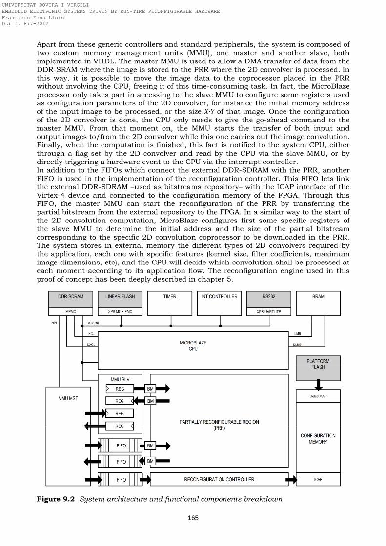
165
Apart from these generic controllers and standard peripherals, the system is composed of two custom memory management units (MMU), one master and another slave, both implemented in VHDL. The master MMU is used to allow a DMA transfer of data from the DDR-SRAM where the image is stored to the PRR where the 2D convolver is processed. In this way, it is possible to move the image data to the coprocessor placed in the PRR without involving the CPU, freeing it of this time-consuming task. In fact, the MicroBlaze processor only takes part in accessing to the slave MMU to configure some registers used as configuration parameters of the 2D convolver, for instance the initial memory address of the input image to be processed, or the size X·Y of that image. Once the configuration of the 2D convolver is done, the CPU only needs to give the go-ahead command to the master MMU. From that moment on, the MMU starts the transfer of both input and output images to/from the 2D convolver while this one carries out the image convolution. Finally, when the computation is finished, this fact is notified to the system CPU, either through a flag set by the 2D convolver and read by the CPU via the slave MMU, or by directly triggering a hardware event to the CPU via the interrupt controller. In addition to the FIFOs which connect the external DDR-SDRAM with the PRR, another FIFO is used in the implementation of the reconfiguration controller. This FIFO lets link the external DDR-SDRAM –used as bitstreams repository– with the ICAP interface of the Virtex-4 device and connected to the configuration memory of the FPGA. Through this FIFO, the master MMU can start the reconfiguration of the PRR by transferring the partial bitstream from the external repository to the FPGA. In a similar way to the start of the 2D convolution computation, MicroBlaze configures first some specific registers of the slave MMU to determine the initial address and the size of the partial bitstream corresponding to the specific 2D convolution coprocessor to be downloaded in the PRR. The system stores in external memory the different types of 2D convolvers required by the application, each one with specific features (kernel size, filter coefficients, maximum image dimensions, etc), and the CPU will decide which convolution shall be processed at each moment according to its application flow. The reconfiguration engine used in this proof of concept has been deeply described in chapter 5.
Figure 9.2 System architecture and functional components breakdown
UNIVERSITAT ROVIRA I VIRGILI EMBEDDED ELECTRONIC SYSTEMS DRIVEN BY RUN-TIME RECONFIGURABLE HARDWARE Francisco Fons Lluís DL: T. 877-2012
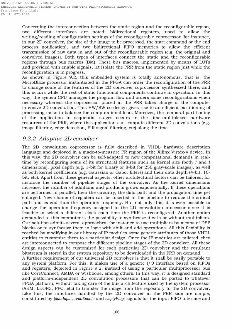
166
Concerning the interconnection between the static region and the reconfigurable region, two different interfaces are noted: bidirectional registers, used to allow the writing/reading of configuration settings of the reconfigurable coprocessor (for instance, in our 2D convolver, the size of the image to be processed, the start command or the end process notification), and two bidirectional FIFO memories to allow the efficient transmission of raw data in and out of the reconfigurable region (e.g. the original and convolved images). Both types of interfaces connect the static and the reconfigurable regions through bus macros (BM). These bus macros, implemented by means of LUTs and provided with enable signals, let isolate the PRR from the static region just while the reconfiguration is in progress. As shown in Figure 9.2, this embedded system is totally autonomous, that is, the MicroBlaze processor instantiated in the FPGA can order the reconfiguration of the PRR to change some of the features of the 2D convolver coprocessor synthesized there, and this occurs while the rest of static functional components continue in operation. In this way, the system CPU manages the program flow and orders some reconfigurations when necessary whereas the coprocessor placed in the PRR takes charge of the compute-intensive 2D convolution. This HW/SW co-design gives rise to an efficient partitioning of processing tasks to balance the computational load. Moreover, the temporal partitioning of the application in sequential stages occurs in the time-multiplexed hardware resources of the PRR, where the application can compute different 2D convolutions (e.g. image filtering, edge detection, FIR signal filtering, etc) along the time.
9.3.2 Adaptive 2D convolver
The 2D convolution coprocessor is fully described in VHDL hardware description language and deployed in a made-to-measure PR region of the Xilinx Virtex-4 device. In this way, the 2D convolver can be self-adapted to new computational demands in real-time by reconfiguring some of its structural features such as kernel size (both J and I dimensions), pixel depth (e.g. 1-bit for binary or 8-bit for 256 gray-scale images), as well as both kernel coefficients (e.g. Gaussian or Gabor filters) and their data depth (4-bit, 16-bit, etc). Apart from these general aspects, other architectural factors can be tailored, for instance the number of pipeline stages of the convolver. As the kernel dimensions increase, the number of additions and products grows exponentially. If these operations are performed in parallel, then the circuitry, the data path and the propagation time get enlarged. New chains of registers can be inserted in the pipeline to reduce the critical path and extend thus the operation frequency. But not only this, it is even possible to change the operation frequency assigned to the 2D convolution processor since it is feasible to select a different clock each time the PRR is reconfigured. Another option demanded to this computer is the possibility to synthesize it with or without multipliers. Our solution admits several approaches, for instance to use multipliers by means of DSP blocks or to synthesize them in logic with shift and add operations. All this flexibility is reached by modifying in our library of IP modules some generic attributes of those VHDL entities to customize them to a particular design. Once the IP modules are tailored, they are interconnected to compose the different pipeline stages of the 2D convolver. All these design aspects can be customized for each particular 2D convolver and the resultant bitstream is stored in the system repository to be downloaded in the PRR on demand. A further requirement of our universal 2D convolver is that it shall be easily portable to any system platform. For this, it makes use of a generic I/O interface based on FIFOs and registers, depicted in Figure 9.2, instead of using a particular multiprocessor bus like CoreConnect, AMBA or Wishbone, among others. In this way, it is designed standard and platform-independent 2D convolution processors that can be ported to whatever FPGA platform, without taking care of the bus architecture used by the system processor (ARM, LEON3, PPC, etc) to transfer the image from the repository to the 2D convolver. Like this, the interfaces handled by the 2D convolver in the PRR side are simple, constituted by dataInput, readEnable and emptyFlag signals for the input FIFO interface and
UNIVERSITAT ROVIRA I VIRGILI EMBEDDED ELECTRONIC SYSTEMS DRIVEN BY RUN-TIME RECONFIGURABLE HARDWARE Francisco Fons Lluís DL: T. 877-2012
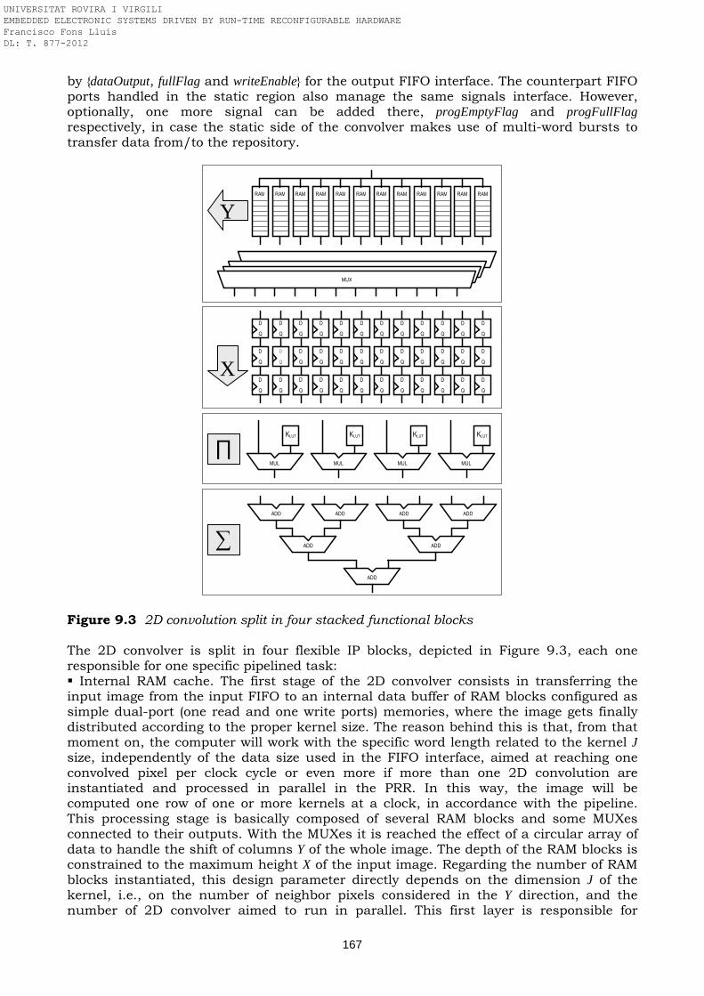
167
by dataOutput, fullFlag and writeEnable for the output FIFO interface. The counterpart FIFO ports handled in the static region also manage the same signals interface. However, optionally, one more signal can be added there, progEmptyFlag and progFullFlag respectively, in case the static side of the convolver makes use of multi-word bursts to transfer data from/to the repository.
ADD
ADD
ADD
ADD
ADD ∑
ADD
ADD
∏
X
Y
MUX
D
Q
D
Q
D
Q
D
Q
D
Q
D
Q
D
Q
D
Q
D
Q
D
Q
D
Q
D
Q
D
Q
D
Q
D
Q
D
Q
D
Q
D
Q
D
Q
D
Q
D
Q
D
Q
D
Q
D
Q
D
Q
D
Q
D
Q
D
Q
D
Q
D
Q
D
Q
D
Q
D
Q
D
Q
D
Q
D
Q
RAM RAM RAM RAM RAM RAM RAM RAM RAM RAM RAM RAM
MUL
MUL
MUL
MUL
KLUT
KLUT
KLUT
KLUT
Figure 9.3 2D convolution split in four stacked functional blocks The 2D convolver is split in four flexible IP blocks, depicted in Figure 9.3, each one responsible for one specific pipelined task: Internal RAM cache. The first stage of the 2D convolver consists in transferring the input image from the input FIFO to an internal data buffer of RAM blocks configured as simple dual-port (one read and one write ports) memories, where the image gets finally distributed according to the proper kernel size. The reason behind this is that, from that moment on, the computer will work with the specific word length related to the kernel J size, independently of the data size used in the FIFO interface, aimed at reaching one convolved pixel per clock cycle or even more if more than one 2D convolution are instantiated and processed in parallel in the PRR. In this way, the image will be computed one row of one or more kernels at a clock, in accordance with the pipeline. This processing stage is basically composed of several RAM blocks and some MUXes connected to their outputs. With the MUXes it is reached the effect of a circular array of data to handle the shift of columns Y of the whole image. The depth of the RAM blocks is constrained to the maximum height X of the input image. Regarding the number of RAM blocks instantiated, this design parameter directly depends on the dimension J of the kernel, i.e., on the number of neighbor pixels considered in the Y direction, and the number of 2D convolver aimed to run in parallel. This first layer is responsible for
UNIVERSITAT ROVIRA I VIRGILI EMBEDDED ELECTRONIC SYSTEMS DRIVEN BY RUN-TIME RECONFIGURABLE HARDWARE Francisco Fons Lluís DL: T. 877-2012
168
shifting the whole image in direction Y with a particular observation: each pixels of the image is transferred only once from its repository to the input FIFO of the 2D convolver. This point shall be noted here because of the need to not stress unnecessarily the bandwidth required in the data transfer from the repository to the input FIFO, given that the repository is usually a shared resource accessible by the core processor and other master controllers in the system, like the 2D convolver. Once a pixel reaches the FIFO and is transferred to the internal RAM cache, it keeps there until it is not required any more, since that pixel takes part in the convolution of the pixel itself and their neighbors limited by the kernel dimensions. The second layer of the pipelined 2D convolver is one or more two-dimensional grids J x I of shift registers organized in columns and with a depth of I registers, delimited by the X coordinate of the kernel in use. As soon as the first (J-1) RAM blocks are filled in with their X pixels and the Jth RAM block receives its first pixel, the start signal is given to the shift registers to start the image shifting row by row in X direction. Once started, this shifting continues for each clock, evolving all the registers together, until the whole image is transferred. The goal of this second layer, concatenated to the previous one in pipeline, consists in shifting the image in the X direction. The composition of these two first stages gives as result the displacement of the image in both Y and X directions, where the control logic for loading the pipe is linear and simple, as shown in Figure 9.4. The third layer takes charge of the product operation. Normally, in modern FPGAs, this operation is performed via hard-wired multipliers located in DSP blocks. Another alternative would be to implement multipliers by consuming logic resources of the FPGA. It is convenient to remark here the possibility of adding in this layer a stage of pre-adders if the kernel has some constant coefficients repeated, e.g. in isotropic filters. This layer of pre-adders lets reduce the effective 2D-convolution, minimizing not only the amount of operations but also the number of parallel hardware multipliers and adders required, as shown later in this work in a concrete implementation example. The last stage is the adder tree where all the partial products are summed. Depending on the kernel dimensions, this stage can require some chains of registers following pipeline and retiming rules. The result of this stage is finally transferred to the output FIFO. Both third and fourth stages can also be implemented together via a vector multiplier approach [Atmel Corp., AN0764, 1999].
Figure 9.4 Parallelism and 4-stage pipeline of the 2D convolver placed in the PRR These four reconfigurable stages of the 2D convolver are placed in the PRR integrated with the rest of system which resides in the static region as highlighted in the block diagram of Figure 9.2. These four generic blocks are connected in pipeline, although depending on the structure of the 2D convolver in some configurations it is not possible to deliver an output in each one clock but in some of them. The interface that connects one stage with the next one consists of a reduced set of data and control lines, typically composed of the inputs dataInput, enableInput, dataValidInput and enableOutput and the outputs dataOutput and dataValidOutput. Figure 9.4 shows the four stages scheduled in time and their connections with the FIFO memories placed in the static region.
FIFO
Y pipe load
X pipe load
Y
X
∏
∑
CLK
n p yx pixels/clk
n p’yx pixels/clk FIFO
UNIVERSITAT ROVIRA I VIRGILI EMBEDDED ELECTRONIC SYSTEMS DRIVEN BY RUN-TIME RECONFIGURABLE HARDWARE Francisco Fons Lluís DL: T. 877-2012
169
9.4 Experimental results
Several 2D convolution examples have been carried out in this section. Thus, the performance evaluation of this proof-of-concept has been compared with other alternatives by means of a set of experiments. Our 2D convolution processing system, implemented in a Xilinx Virtex-4 XC4VLX25 FPGA, exploits both hardware/software co-design and run-time reconfigurable computing techniques in search of a cost-effective solution able to be integrated in whatever low cost, high performance embedded application. Next, it is described the main PR features of the Virtex-4 device.
9.4.1 Virtex-4 FPGA
This section shows a brief overview of the Virtex-4 FPGA from a pure PR perspective, highlighting those features which have a notorious impact on the dynamic partial self-reconfiguration concept exploited in this work: Virtex-4 devices have glitchless reconfiguration. This feature enables static routes to cross PR regions, fact that simplifies the routing constraints for building a PR design and permits to optimize the system placement and routing. Thus, although in the PRR all the combinational (LUTs) and sequential (flip flops) resources of the configurable logic blocks (CLBs) are automatically reserved to the PR modules, the routing resources are enabled to be used by the static region, which must stay invariant in all the reconfigured PRMs. In this way, they will not be affected by the run-time reconfiguration; that is, as long as the static routes are implemented identically in every PRM, no glitches will occur on them when overwriting these bits with the same values they already have. Therefore, these static routes in the PRR are not affected when PRMs are reconfigured. Regarding reconfiguration grain, Virtex-4 admits a PR granularity of a bit-wise frame of 16 CLBs tall, where a configuration frame consists of forty-one 32-bit words. In this way, it is feasible to dynamically reconfigure 2D regions as small as 16 CLBs rows high and 1-bit wide. Virtex-4 devices are equipped with an internal interface called ICAP (Internal Configuration Access Port) which enables the device itself to carry out the reconfiguration of some region of the device –just the one not affecting the ICAP circuitry– through a specific reconfiguration controller synthesized with own resources of the device, and at run-time, while the rest of the device continues the operation undisturbed. Furthermore, the ICAP interface of Virtex-4 devices delivers a greater bandwidth in comparison to former FPGA families. This aspect is especially relevant for run-time PR applications. The internal reconfiguration port admits 32-bit data bus to transfer the partial bitstreams at a maximum frequency of 100MHz. Both features, finer reconfiguration granularity and higher reconfiguration bandwidth lets minimize the impact in time of the reconfiguration latency on any time-critical compute-intensive application. Although Virtex-4, -5 and -6 FPGA families deliver the same maximum reconfiguration rate, Virtex-4 was the first and only family which fully supported a mature PR design flow at the moment of developing this work, especially regarding toolset availability. The tools for the other two families, Virtex-5 and Virtex-6, although also incorporated to the PR design flow, were still in development in the moment this work was carried out. Just for this reason, this work focused on Virtex-4 to implement a reconfigurable 2D convolution computer.
9.4.2 Performance evaluation
Virtex-4 is probably the first device equipped with a level of PR performance –both technological aspects and supported development tools– acceptable for industrial and commercial perspectives. The design flow followed is based on modular design: it allows designs to be split into modules that are coded, synthesized, mapped, placed and routed independently. The toolset used in this work, available in the Xilinx Early Access Partial
UNIVERSITAT ROVIRA I VIRGILI EMBEDDED ELECTRONIC SYSTEMS DRIVEN BY RUN-TIME RECONFIGURABLE HARDWARE Francisco Fons Lluís DL: T. 877-2012
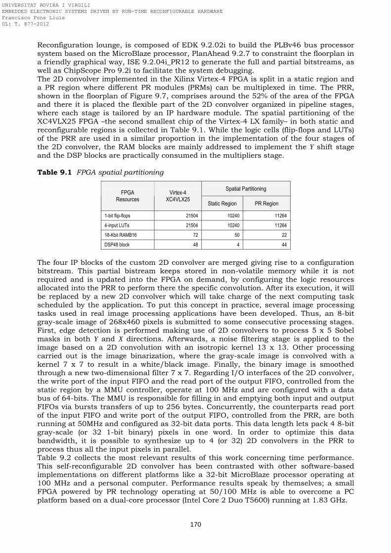
170
Reconfiguration lounge, is composed of EDK 9.2.02i to build the PLBv46 bus processor system based on the MicroBlaze processor, PlanAhead 9.2.7 to constraint the floorplan in a friendly graphical way, ISE 9.2.04i_PR12 to generate the full and partial bitstreams, as well as ChipScope Pro 9.2i to facilitate the system debugging. The 2D convolver implemented in the Xilinx Virtex-4 FPGA is split in a static region and a PR region where different PR modules (PRMs) can be multiplexed in time. The PRR, shown in the floorplan of Figure 9.7, comprises around the 52% of the area of the FPGA and there it is placed the flexible part of the 2D convolver organized in pipeline stages, where each stage is tailored by an IP hardware module. The spatial partitioning of the XC4VLX25 FPGA –the second smallest chip of the Virtex-4 LX family– in both static and reconfigurable regions is collected in Table 9.1. While the logic cells (flip-flops and LUTs) of the PRR are used in a similar proportion in the implementation of the four stages of the 2D convolver, the RAM blocks are mainly addressed to implement the Y shift stage and the DSP blocks are practically consumed in the multipliers stage. Table 9.1 FPGA spatial partitioning
Spatial Partitioning FPGA
Resources Virtex-4
XC4VLX25 Static Region PR Region
1-bit flip-flops 21504 10240 11264
4-input LUTs 21504 10240 11264
18-Kbit RAMB16 72 50 22
DSP48 block 48 4 44
The four IP blocks of the custom 2D convolver are merged giving rise to a configuration bitstream. This partial bistream keeps stored in non-volatile memory while it is not required and is updated into the FPGA on demand, by configuring the logic resources allocated into the PRR to perform there the specific convolution. After its execution, it will be replaced by a new 2D convolver which will take charge of the next computing task scheduled by the application. To put this concept in practice, several image processing tasks used in real image processing applications have been developed. Thus, an 8-bit gray-scale image of 268x460 pixels is submitted to some consecutive processing stages. First, edge detection is performed making use of 2D convolvers to process 5 x 5 Sobel masks in both Y and X directions. Afterwards, a noise filtering stage is applied to the image based on a 2D convolution with an isotropic kernel 13 x 13. Other processing carried out is the image binarization, where the gray-scale image is convolved with a kernel 7 x 7 to result in a white/black image. Finally, the binary image is smoothed through a new two-dimensional filter 7 x 7. Regarding I/O interfaces of the 2D convolver, the write port of the input FIFO and the read port of the output FIFO, controlled from the static region by a MMU controller, operate at 100 MHz and are configured with a data bus of 64-bits. The MMU is responsible for filling in and emptying both input and output FIFOs via bursts transfers of up to 256 bytes. Concurrently, the counterparts read port of the input FIFO and write port of the output FIFO, controlled from the PRR, are both running at 50MHz and configured as 32-bit data ports. This data length lets pack 4 8-bit gray-scale (or 32 1-bit binary) pixels in one word. In order to optimize this data bandwidth, it is possible to synthesize up to 4 (or 32) 2D convolvers in the PRR to process thus all the input pixels in parallel. Table 9.2 collects the most relevant results of this work concerning time performance. This self-reconfigurable 2D convolver has been contrasted with other software-based implementations on different platforms like a 32-bit MicroBlaze processor operating at 100 MHz and a personal computer. Performance results speak by themselves; a small FPGA powered by PR technology operating at 50/100 MHz is able to overcome a PC platform based on a dual-core processor (Intel Core 2 Duo T5600) running at 1.83 GHz.
UNIVERSITAT ROVIRA I VIRGILI EMBEDDED ELECTRONIC SYSTEMS DRIVEN BY RUN-TIME RECONFIGURABLE HARDWARE Francisco Fons Lluís DL: T. 877-2012
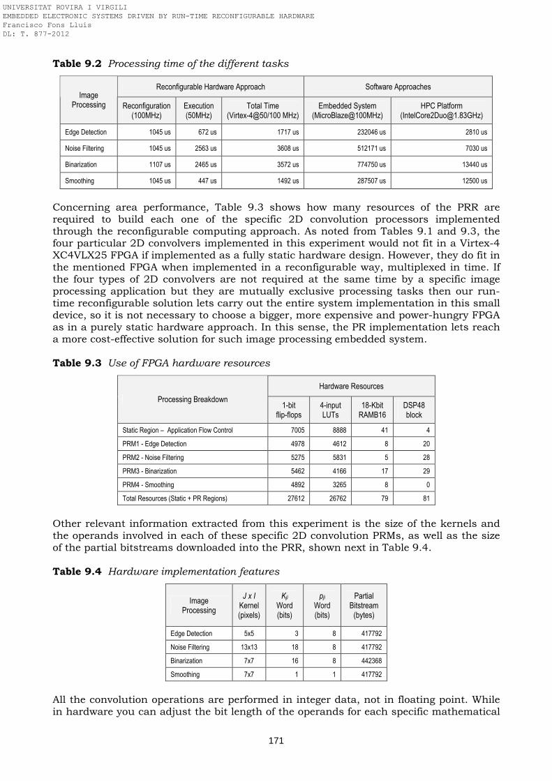
171
Table 9.2 Processing time of the different tasks
Reconfigurable Hardware Approach Software Approaches Image
Processing Reconfiguration (100MHz)
Execution (50MHz)
Total Time (Virtex-4@50/100 MHz)
Embedded System (MicroBlaze@100MHz)
HPC Platform ([email protected])
Edge Detection 1045 us 672 us 1717 us 232046 us 2810 us
Noise Filtering 1045 us 2563 us 3608 us 512171 us 7030 us
Binarization 1107 us 2465 us 3572 us 774750 us 13440 us
Smoothing 1045 us 447 us 1492 us 287507 us 12500 us
Concerning area performance, Table 9.3 shows how many resources of the PRR are required to build each one of the specific 2D convolution processors implemented through the reconfigurable computing approach. As noted from Tables 9.1 and 9.3, the four particular 2D convolvers implemented in this experiment would not fit in a Virtex-4 XC4VLX25 FPGA if implemented as a fully static hardware design. However, they do fit in the mentioned FPGA when implemented in a reconfigurable way, multiplexed in time. If the four types of 2D convolvers are not required at the same time by a specific image processing application but they are mutually exclusive processing tasks then our run-time reconfigurable solution lets carry out the entire system implementation in this small device, so it is not necessary to choose a bigger, more expensive and power-hungry FPGA as in a purely static hardware approach. In this sense, the PR implementation lets reach a more cost-effective solution for such image processing embedded system. Table 9.3 Use of FPGA hardware resources
Hardware Resources
Processing Breakdown 1-bit
flip-flops 4-input LUTs
18-Kbit RAMB16
DSP48 block
Static Region – Application Flow Control 7005 8888 41 4
PRM1 - Edge Detection 4978 4612 8 20
PRM2 - Noise Filtering 5275 5831 5 28
PRM3 - Binarization 5462 4166 17 29
PRM4 - Smoothing 4892 3265 8 0
Total Resources (Static + PR Regions) 27612 26762 79 81
Other relevant information extracted from this experiment is the size of the kernels and the operands involved in each of these specific 2D convolution PRMs, as well as the size of the partial bitstreams downloaded into the PRR, shown next in Table 9.4. Table 9.4 Hardware implementation features
Image Processing
J x I Kernel (pixels)
Kji Word (bits)
pji Word (bits)
Partial Bitstream
(bytes)
Edge Detection 5x5 3 8 417792
Noise Filtering 13x13 18 8 417792
Binarization 7x7 16 8 442368
Smoothing 7x7 1 1 417792
All the convolution operations are performed in integer data, not in floating point. While in hardware you can adjust the bit length of the operands for each specific mathematical
UNIVERSITAT ROVIRA I VIRGILI EMBEDDED ELECTRONIC SYSTEMS DRIVEN BY RUN-TIME RECONFIGURABLE HARDWARE Francisco Fons Lluís DL: T. 877-2012
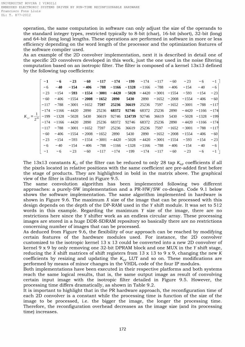
172
operation, the same computation in software can only adjust the size of the operands to the standard integer types, restricted typically to 8-bit (char), 16-bit (short), 32-bit (long) and 64-bit (long long) lengths. These operations are performed in software in more or less efficiency depending on the word length of the processor and the optimization features of the software compiler used. As an example of the 2D convolver implementation, next it is described in detail one of the specific 2D convolvers developed in this work, just the one used in the noise filtering computation based on an isotropic filter. The filter is composed of a kernel 13x13 defined by the following tap coefficients:
−−−−−−−−−−−−−−−−−−−−−−−−−−−−−−−−−−−−−−−−−−−−−−−−−−−−−−−−−−−−−−−−−−−−−−−−−−−−−−−−−−−−−−−−−−−−−−−−−−−−−−−−−−−−−−−−−−−−−−−−−−−−−−−−−−−−
=
162360117174199174117602361
640154406788116613281166788406154406
23154593155430014420502844203001155459315423
6040615542008165228905430289016522008155440660
117788300116527597252363661925236759716523001788117
1741166442028902523668372927466837225236289044201166174
19913285028543036619927469274636619543050281328199
174116644202890252366837225236289044201166174
1177883001165275972523616523001788117
604061554200816522890155440660
2315459315543001442015423
64015440678811666
162360117174
2
120, 124739
9274668372
36619252367597
5430289016522008
5028442030011554593
1328116678840615440
199174117602361
ijK
The 13x13 constants Kj,i of the filter can be reduced to only 28 tap Kq,p coefficients if all the pixels located in relative positions with the same coefficient are pre-added first before the stage of products. They are highlighted in bold in the matrix above. The graphical view of the filter is illustrated in Figure 9.5. The same convolution algorithm has been implemented following two different approaches: a purely-SW implementation and a PR-HW/SW co-design. Code 9.1 below shows the software implementation. The same algorithm implemented in hardware is shown in Figure 9.6. The maximum X size of the image that can be processed with this design depends on the depth of the DP-RAM used in the Y shift module. It was set to 512 words in this example. Regarding the maximum Y size of the image, there are no restrictions here since the Y shifter work as an endless circular array. These processing images are stored in a huge DDR-SDRAM repository so basically there are no restrictions concerning number of images that can be processed. As deduced from Figure 9.6, the flexibility of our approach can be reached by modifying certain features of the hardware modules used. For instance, the 2D convolver customized to the isotropic kernel 13 x 13 could be converted into a new 2D convolver of kernel 9 x 9 by only removing one 32-bit DPRAM block and one MUX in the Y shift stage, reducing the X shift matrices of shift registers from 13 x 13 to 9 x 9, changing the new K coefficients by resizing and updating the Kq,p LUT and so on. These modifications are performed by means of minor changes in the VHDL code of the four IP modules. Both implementations have been executed in their respective platforms and both systems reach the same logical results, that is, the same output image as result of convolving certain input image with the isotropic filter detailed in Figure 9.5. However, the processing time differs dramatically, as shown in Table 9.2. It is important to highlight that in the PR hardware approach, the reconfiguration time of each 2D convolver is a constant while the processing time is function of the size of the image to be processed, i.e. the bigger the image, the longer the processing time. Therefore, the reconfiguration overhead decreases as the image size (and its processing time) increases.
UNIVERSITAT ROVIRA I VIRGILI EMBEDDED ELECTRONIC SYSTEMS DRIVEN BY RUN-TIME RECONFIGURABLE HARDWARE Francisco Fons Lluís DL: T. 877-2012
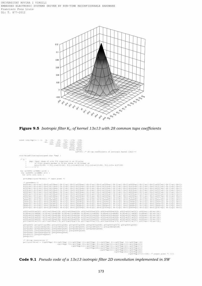
173
y0-6
y0-5
y0-4
y0-3
y0-2
y0-1
y0
y0+1
y0+2
y0+3
y0+4
y0+5
y0+6 x0-6
x0-5x0-4
x0-3
x0-2x0-1
x0x0+1
x0+2x0+3
x0+4x0+5
x0+6-0,02
0
0,02
0,04
0,06
0,08
0,1
0,12
Figure 9.5 Isotropic filter Kj,i of kernel 13x13 with 28 common taps coefficients const long Kqp[]= -1, -6, -23, -60, -117, -174, -199, -40, -154, -406, -788, -1166, -1328, -593, -1554, -3001, -4420, -5028, -2008, -1652, 2890, 5430, 7597, 25236, 36619, 68372, 92746, 124739; /* 28 tap coefficients of isotropic kernel 13x13 */ void NoiseFiltering(unsigned char *bmp) /* X ^ | bmp: input image of size Y*X organized in an 1D-array | of 8-bit pixels packed in 32-bit words in 2D-format as | bits31:00) -> P(j,i)=b[31:24], P(j,i+1)=b[23:16] P(j,i+2)=b[15:08], P(j,i+3)= b[07:00] +------> Y */ for (y=YSTT; y<YEND; y+=4) for (x=XSTT; x<=XEND; x++) for (z=0; z<4; z++) pi=&(bmp[((y+z)*X)+x]); /* input pixel */ /* preadders */ p000C=pi[-6X-6]+pi[-6X+6];p010B=pi[-6X-5]+pi[-6X+5];p020A=pi[-6X-4]+pi[-6X+4];p0309=pi[-6X-3]+pi[-6X+3];p0408=pi[-6X-2]+pi[-6X+2];p0507=pi[-6X-1]+pi[-6X+1]; p101C=pi[-5X-6]+pi[-5X+6];p111B=pi[-5X-5]+pi[-5X+5];p121A=pi[-5X-4]+pi[-5X+4];p1319=pi[-5X-3]+pi[-5X+3];p1418=pi[-5X-2]+pi[-5X+2];p1517=pi[-5X-1]+pi[-5X+1]; p202C=pi[-4X-6]+pi[-4X+6];p212B=pi[-4X-5]+pi[-4X+5];p222A=pi[-4X-4]+pi[-4X+4];p2329=pi[-4X-3]+pi[-4X+3];p2428=pi[-4X-2]+pi[-4X+2];p2527=pi[-4X-1]+pi[-4X+1]; p303C=pi[-3X-6]+pi[-3X+6];p313B=pi[-3X-5]+pi[-3X+5];p323A=pi[-3X-4]+pi[-3X+4];p3339=pi[-3X-3]+pi[-3X+3];p3438=pi[-3X-2]+pi[-3X+2];p3537=pi[-3X-1]+pi[-3X+1]; p404C=pi[-2X-6]+pi[-2X+6];p414B=pi[-2X-5]+pi[-2X+5];p424A=pi[-2X-4]+pi[-2X+4];p4349=pi[-2X-3]+pi[-2X+3];p4448=pi[-2X-2]+pi[-2X+2];p4547=pi[-2X-1]+pi[-2X+1]; p505C=pi[-1X-6]+pi[-1X+6];p515B=pi[-1X-5]+pi[-1X+5];p525A=pi[-1X-4]+pi[-1X+4];p5359=pi[-1X-3]+pi[-1X+3];p5458=pi[-1X-2]+pi[-1X+2];p5557=pi[-1X-1]+pi[-1X+1]; p606C=pi[ 0X-6]+pi[ 0X+6];p616B=pi[ 0X-5]+pi[ 0X+5];p626A=pi[ 0X-4]+pi[ 0X+4];p6369=pi[ 0X-3]+pi[ 0X+3];p6468=pi[ 0X-2]+pi[ 0X+2];p6567=pi[ 0X-1]+pi[ 0X+1]; p707C=pi[ 1X-6]+pi[ 1X+6];p717B=pi[ 1X-5]+pi[ 1X+5];p727A=pi[ 1X-4]+pi[ 1X+4];p7379=pi[ 1X-3]+pi[ 1X+3];p7478=pi[ 1X-2]+pi[ 1X+2];p7577=pi[ 1X-1]+pi[ 1X+1]; p808C=pi[ 2X-6]+pi[ 2X+6];p818B=pi[ 2X-5]+pi[ 2X+5];p828A=pi[ 2X-4]+pi[ 2X+4];p8389=pi[ 2X-3]+pi[ 2X+3];p8488=pi[ 2X-2]+pi[ 2X+2];p8587=pi[ 2X-1]+pi[ 2X+1]; p909C=pi[ 3X-6]+pi[ 3X+6];p919B=pi[ 3X-5]+pi[ 3X+5];p929A=pi[ 3X-4]+pi[ 3X+4];p9399=pi[ 3X-3]+pi[ 3X+3];p9498=pi[ 3X-2]+pi[ 3X+2];p9597=pi[ 3X-1]+pi[ 3X+1]; pA0AC=pi[ 4X-6]+pi[ 4X+6];pA1AB=pi[ 4X-5]+pi[ 4X+5];pA2AA=pi[ 4X-4]+pi[ 4X+4];pA3A9=pi[ 4X-3]+pi[ 4X+3];pA4A8=pi[ 4X-2]+pi[ 4X+2];pA5A7=pi[ 4X-1]+pi[ 4X+1]; pB0BC=pi[ 5X-6]+pi[ 5X+6];pB1BB=pi[ 5X-5]+pi[ 5X+5];pB2BA=pi[ 5X-4]+pi[ 5X+4];pB3B9=pi[ 5X-3]+pi[ 5X+3];pB4B8=pi[ 5X-2]+pi[ 5X+2];pB5B7=pi[ 5X-1]+pi[ 5X+1]; pC0CC=pi[ 6X-6]+pi[ 6X+6];pC1CB=pi[ 6X-5]+pi[ 6X+5];pC2CA=pi[ 6X-4]+pi[ 6X+4];pC3C9=pi[ 6X-3]+pi[ 6X+3];pC4C8=pi[ 6X-2]+pi[ 6X+2];pC5C7=pi[ 6X-1]+pi[ 6X+1]; p00C0=p000C+pC0CC; p01C1=p010B+pC1CB; p02C2=p020A+pC2CA; p03C3=p0309+pC3C9; p04C4=p0408+pC4C8; p05C5=p0507+pC5C7; p06C6=pi[-6X]+pi[6X]; p10B0=p101C+pB0BC; p11B1=p111B+pB1BB; p12B2=p121A+pB2BA; p13B3=p1319+pB3B9; p14B4=p1418+pB4B8; p15B5=p1517+pB5B7; p16B6=pi[-5X]+pi[5X]; p20A0=p202C+pA0AC; p21A1=p212B+pA1AB; p22A2=p222A+pA2AA; p23A3=p2329+pA3A9; p24A4=p2428+pA4A8; p25A5=p2527+pA5A7; p26A6=pi[-4X]+pi[4X]; p3090=p303C+p909C; p3191=p313B+p919B; p3292=p323A+p929A; p3393=p3339+p9399; p3494=p3438+p9498; p3595=p3537+p9597; p3696=pi[-3X]+pi[3X]; p4080=p404C+p808C; p4181=p414B+p818B; p4282=p424A+p828A; p4383=p4349+p8389; p4484=p4448+p8488; p4585=p4547+p8587; p4686=pi[-2X]+pi[2X]; p5070=p505C+p707C; p5171=p515B+p717B; p5272=p525A+p727A; p5373=p5359+p7379; p5474=p5458+p7478; p5575=p5557+p7577; p5676=pi[-1X]+pi[1X]; p00=p00C0; p01=p01C1+p10B0; p02=p02C2+p20A0; p03=p03C3+p3090; p04=p04C4+p4080; p05=p05C5+p5070; p06=p06C6+p606C; p11=p11B1; p12=p12B2+p21A1; p13=p13B3+p3191; p14=p14B4+p4181; p15=p15B5+p5171; p16=p16B6+p616B; p22=p22A2; p23=p23A3+p3292; p24=p24A4+p4282; p25=p25A5+p5272; p26=p26A6+p626A; p33=p3393; p34=p3494+p4383; p35=p3595+p5373; p36=p3696+p6369; p44=p4484; p45=p4585+p5474; p46=p4686+p6468; p55=p5575; p56=p5676+p6567; p66=pi[0]; /* 28-tap convolution */ po[((y+z)*X)+x] = (((p00*Kqp[ 0])+(p01*Kqp[ 1])+(p02*Kqp[ 2])+(p03*Kqp[ 3])+(p04*Kqp[ 4])+(p05*Kqp[ 5])+(p06*Kqp[ 6]) +(p11*Kqp[ 7])+(p12*Kqp[ 8])+(p13*Kqp[ 9])+(p14*Kqp[10])+(p15*Kqp[11])+(p16*Kqp[12]) +(p22*Kqp[13])+(p23*Kqp[14])+(p24*Kqp[15])+(p25*Kqp[16])+(p26*Kqp[17]) +(p33*Kqp[18])+(p34*Kqp[19])+(p35*Kqp[20])+(p36*Kqp[21]) +(p44*Kqp[22])+(p45*Kqp[23])+(p46*Kqp[24]) +(p55*Kqp[25])+(p56*Kqp[26]) +(p66*Kqp[27]))>>20); /* output pixel */
Code 9.1 Pseudo code of a 13x13 isotropic filter 2D convolution implemented in SW
UNIVERSITAT ROVIRA I VIRGILI EMBEDDED ELECTRONIC SYSTEMS DRIVEN BY RUN-TIME RECONFIGURABLE HARDWARE Francisco Fons Lluís DL: T. 877-2012
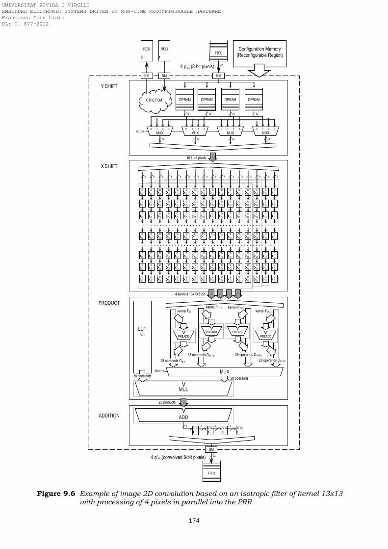
174
Figure 9.6 Example of image 2D convolution based on an isotropic filter of kernel 13x13
with processing of 4 pixels in parallel into the PRR
Configuration Memory (Reconfigurable Region)
DPRAM
SEL[1:0]
D
Q
D
Q
D
Q
D
Q
D
Q
D
Q
D
Q
D
Q
D
Q
D
Q
D
Q
D
Q
D
Q
D
Q
D
Q
D
Q
D
Q
D
Q
D
Q
D
Q
D
Q
D
Q
D
Q
D
Q
D
Q
D
Q
D
Q
D
Q
D
Q
D
Q
D
Q
D
Q
D
Q
D
Q
D
Q
D
Q
D
Q
D
Q
D
Q
D
Q
D
Q
D
Q
D
Q
D
Q
D
Q
Pj+3,i
D
Q
D
Q
D
Q
D
Q
D
Q
D
Q
Pj+2,i
D
Q
D
Q
D
Q
D
Q
D
Q
D
Q
Pj+1,i
D
Q
D
Q
D
Q
D
Q
D
Q
D
Q
Pj,i
D
Q
D
Q
D
Q
D
Q
D
Q
D
Q
D
Q
D
Q
D
Q
D
Q
D
Q
D
Q
D
Q
D
Q
D
Q
D
Q
D
Q
D
Q
D
Q
D
Q
D
Q
D
Q
D
Q
D
Q
D
Q
D
Q
D
Q
D
Q
D
Q
D
Q
D
Q
D
Q
D
Q
D
Q
D
Q
D
Q
D
Q
D
Q
D
Q
D
Q
D
Q
D
Q
D
Q
D
Q
D
Q
DPRAM DPRAM DPRAM
32 32 32 32
0 1 2 3
MUX
0 1 2 3
MUX
0 1 2 3
MUX
0 1 2 3
MUX
32 32 32 32
8 8 8 8 8 8 8 8 8 8 8 8 8 8 8 8
32
CTRL FSM
PREADD
MUX
16 8-bit pixels
4 kernels 13x13 8-bit
LUT Kq,p
PREADD
MUL
ADD
8 8
FIFO
32
REG REG
BM BM BM
BM
. . . . . . . . . . . . . . . . . . . . . . . . . . . . . . . . . . . . . . . . . . . . .
. . . . . . . . . . . . . . . . . . . . . . . . . . . . . . . . . . . . . . . . . . . . .
Y SHIFT
PREADD
PREADD
28 operands Oq,p
28 constants
28 operands Oq+1,p
28 operands Oq+3,p
28 operands Oq+2,p
28 products
4 p’yx (convolved 8-bit pixels)
4 p yx (8-bit pixels)
X SHIFT
PRODUCT
ADDITION
kernel Pj,i kernel Pj+1,i kernel Pj+2,i
kernel Pj+3,i
D Q 8
D Q 8
D Q D Q
28 operands
FIFO
SELK[1:0]
UNIVERSITAT ROVIRA I VIRGILI EMBEDDED ELECTRONIC SYSTEMS DRIVEN BY RUN-TIME RECONFIGURABLE HARDWARE Francisco Fons Lluís DL: T. 877-2012
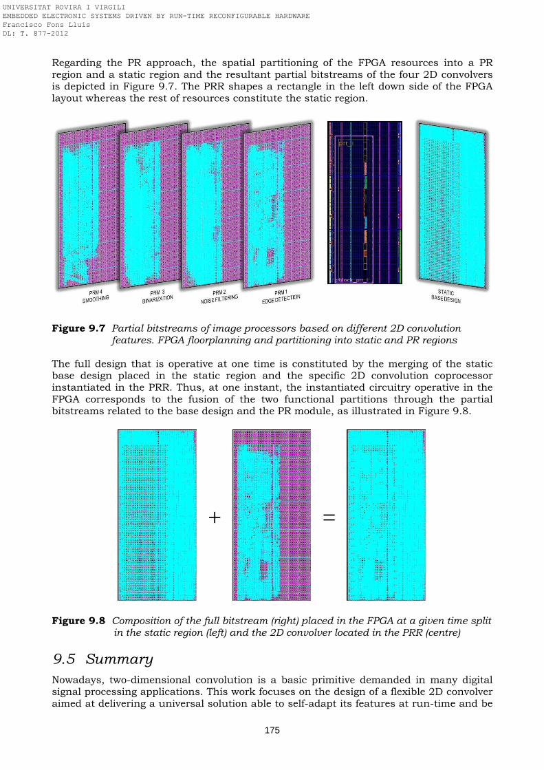
175
Regarding the PR approach, the spatial partitioning of the FPGA resources into a PR region and a static region and the resultant partial bitstreams of the four 2D convolvers is depicted in Figure 9.7. The PRR shapes a rectangle in the left down side of the FPGA layout whereas the rest of resources constitute the static region.
Figure 9.7 Partial bitstreams of image processors based on different 2D convolution
features. FPGA floorplanning and partitioning into static and PR regions The full design that is operative at one time is constituted by the merging of the static base design placed in the static region and the specific 2D convolution coprocessor instantiated in the PRR. Thus, at one instant, the instantiated circuitry operative in the FPGA corresponds to the fusion of the two functional partitions through the partial bitstreams related to the base design and the PR module, as illustrated in Figure 9.8.
= +
Figure 9.8 Composition of the full bitstream (right) placed in the FPGA at a given time split
in the static region (left) and the 2D convolver located in the PRR (centre)
9.5 Summary
Nowadays, two-dimensional convolution is a basic primitive demanded in many digital signal processing applications. This work focuses on the design of a flexible 2D convolver aimed at delivering a universal solution able to self-adapt its features at run-time and be
UNIVERSITAT ROVIRA I VIRGILI EMBEDDED ELECTRONIC SYSTEMS DRIVEN BY RUN-TIME RECONFIGURABLE HARDWARE Francisco Fons Lluís DL: T. 877-2012
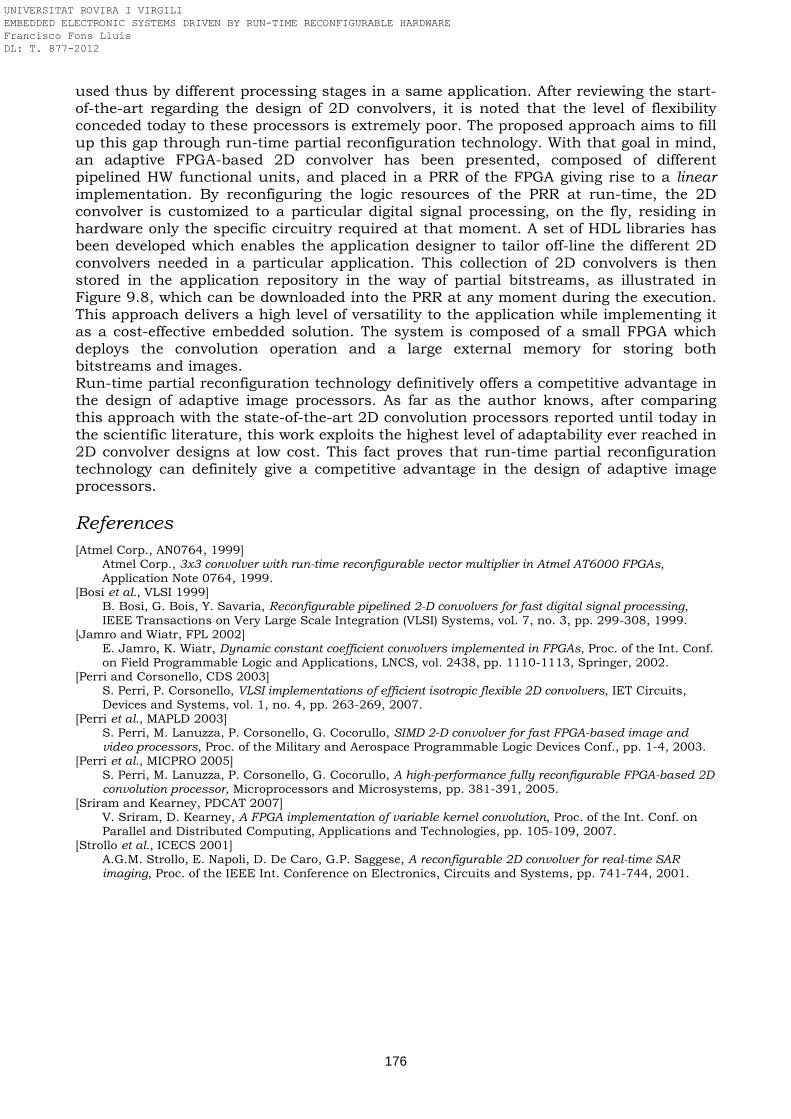
176
used thus by different processing stages in a same application. After reviewing the start-of-the-art regarding the design of 2D convolvers, it is noted that the level of flexibility conceded today to these processors is extremely poor. The proposed approach aims to fill up this gap through run-time partial reconfiguration technology. With that goal in mind, an adaptive FPGA-based 2D convolver has been presented, composed of different pipelined HW functional units, and placed in a PRR of the FPGA giving rise to a linear implementation. By reconfiguring the logic resources of the PRR at run-time, the 2D convolver is customized to a particular digital signal processing, on the fly, residing in hardware only the specific circuitry required at that moment. A set of HDL libraries has been developed which enables the application designer to tailor off-line the different 2D convolvers needed in a particular application. This collection of 2D convolvers is then stored in the application repository in the way of partial bitstreams, as illustrated in Figure 9.8, which can be downloaded into the PRR at any moment during the execution. This approach delivers a high level of versatility to the application while implementing it as a cost-effective embedded solution. The system is composed of a small FPGA which deploys the convolution operation and a large external memory for storing both bitstreams and images. Run-time partial reconfiguration technology definitively offers a competitive advantage in the design of adaptive image processors. As far as the author knows, after comparing this approach with the state-of-the-art 2D convolution processors reported until today in the scientific literature, this work exploits the highest level of adaptability ever reached in 2D convolver designs at low cost. This fact proves that run-time partial reconfiguration technology can definitely give a competitive advantage in the design of adaptive image processors.
References
[Atmel Corp., AN0764, 1999] Atmel Corp., 3x3 convolver with run-time reconfigurable vector multiplier in Atmel AT6000 FPGAs, Application Note 0764, 1999.
[Bosi et al., VLSI 1999] B. Bosi, G. Bois, Y. Savaria, Reconfigurable pipelined 2-D convolvers for fast digital signal processing, IEEE Transactions on Very Large Scale Integration (VLSI) Systems, vol. 7, no. 3, pp. 299-308, 1999.
[Jamro and Wiatr, FPL 2002] E. Jamro, K. Wiatr, Dynamic constant coefficient convolvers implemented in FPGAs, Proc. of the Int. Conf. on Field Programmable Logic and Applications, LNCS, vol. 2438, pp. 1110-1113, Springer, 2002.
[Perri and Corsonello, CDS 2003] S. Perri, P. Corsonello, VLSI implementations of efficient isotropic flexible 2D convolvers, IET Circuits, Devices and Systems, vol. 1, no. 4, pp. 263-269, 2007.
[Perri et al., MAPLD 2003] S. Perri, M. Lanuzza, P. Corsonello, G. Cocorullo, SIMD 2-D convolver for fast FPGA-based image and video processors, Proc. of the Military and Aerospace Programmable Logic Devices Conf., pp. 1-4, 2003.
[Perri et al., MICPRO 2005] S. Perri, M. Lanuzza, P. Corsonello, G. Cocorullo, A high-performance fully reconfigurable FPGA-based 2D convolution processor, Microprocessors and Microsystems, pp. 381-391, 2005.
[Sriram and Kearney, PDCAT 2007] V. Sriram, D. Kearney, A FPGA implementation of variable kernel convolution, Proc. of the Int. Conf. on Parallel and Distributed Computing, Applications and Technologies, pp. 105-109, 2007.
[Strollo et al., ICECS 2001] A.G.M. Strollo, E. Napoli, D. De Caro, G.P. Saggese, A reconfigurable 2D convolver for real-time SAR imaging, Proc. of the IEEE Int. Conference on Electronics, Circuits and Systems, pp. 741-744, 2001.
UNIVERSITAT ROVIRA I VIRGILI EMBEDDED ELECTRONIC SYSTEMS DRIVEN BY RUN-TIME RECONFIGURABLE HARDWARE Francisco Fons Lluís DL: T. 877-2012
177
Chapter 10 Trigonometric CORDIC computer Trigonometrics is present in many signal processing fields. An implementation alternative of the trigonometric computing is the CORDIC (COordinate Rotation DIgital Computer) algorithm. Essentially, by rotating a two-dimensional vector in linear, circular and hyperbolic coordinate systems, CORDIC lets perform products/divisions, trigonometric and hyperbolic functions, respectively. The rotation is carried out through a sequence of iterations; one micro rotation of a prefixed elementary angle is performed for each iteration by means of addition-shift operations, being the rotated vector scaled by a constant factor that is then compensated. CORDIC is attractive for the computing of elementary functions due to its simplicity and accuracy. However, the main benefit of the CORDIC algorithm is its easy implementation in hardware, consisting basically of three adders-substractors, two shift registers and one LUT of precomputed elementary angles. Besides, this iterative algorithm can be synthesized unrolled by inserting registers in each adder-substractor stage, enabling thus a pipelined computation. This chapter deals with the implementation of a trigonometric CORDIC computer making use of run-time reconfigurable hardware. Two approaches are presented: one exploiting the fine-grain reconfiguration of the different CORDIC elementary functions and the other exploiting the coarse-grain reconfiguration of the full computing unit. The first option permits to implement different mathematical functions over the same computational hardware skeleton, achieving a versatile computer thanks to small functional changes performed with run-time reconfiguration. The other approach describes the implementation of a trigonometric CORDIC coprocessor which is swapped in and out of a partially reconfigurable region of the computing system where different coprocessors are multiplexed in time during the execution of an application.
10.1 Introduction
Nowadays, the trigonometric computing is exploited in many engineering fields. As example, global positioning and navigation systems responsible for calculating trajectories in real-time (robots, satellites, radars, etc) make use of Trigonometrics. A well-known technique for trigonometric calculus is the CORDIC algorithm, characterized by its implementation simplicity, efficiency and elegance. Originally credited to Volder [Volder, IRETEC 1959] and generalized later by Walther [Walther, SJCC 1971], the CORDIC concept consists in rotating a 2D vector a desired angle φ along a circular, linear or hyperbolic coordinate system decomposing it into a sum of predefined elementary angles φi such that, iteratively in each step i, the rotated angle φi can be expressed as a value that depends on the i-th power of 2, what finally is computed by simple binary shifts and additions, and where the result is more and more accurate as the number of iterations increases since the vector orientation is successively closer to its target or convergence point. The use of FPGAs emerged as a viable means of offsetting microprocessor performance limitations in applications that require high-speed processing of large data, as CORDIC computing. Standard DSP processors can be ill-suited to perform at the required rates due to the serial nature of their architecture or to the lack of certain instructions set extension. FPGAs have been successfully used to mitigate these problems by performing them in hardware, bypassing the sequential stored-program techniques in favour of parallel and dedicated logic functions. Moreover, the multi-purpose CORDIC algorithm exhibits additional characteristics useful to implement by evolvable hardware because of the high similarity among its different operation modes. Implementation examples of
UNIVERSITAT ROVIRA I VIRGILI EMBEDDED ELECTRONIC SYSTEMS DRIVEN BY RUN-TIME RECONFIGURABLE HARDWARE Francisco Fons Lluís DL: T. 877-2012
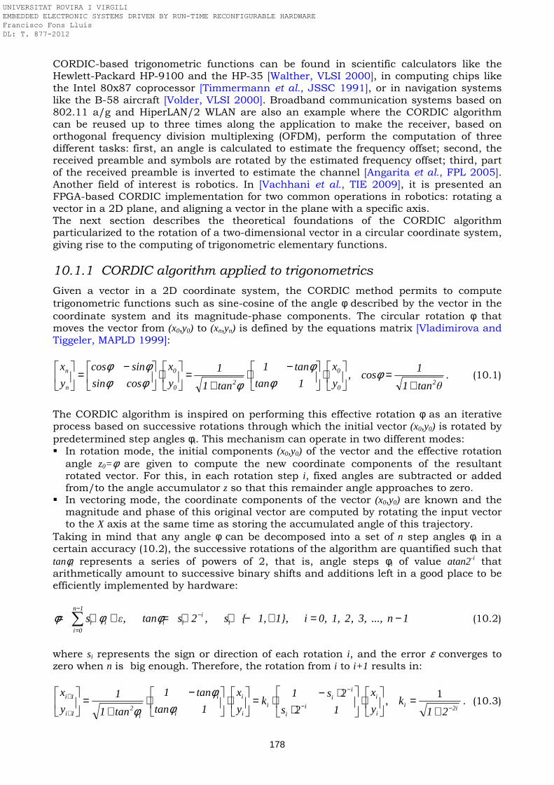
178
CORDIC-based trigonometric functions can be found in scientific calculators like the Hewlett-Packard HP-9100 and the HP-35 [Walther, VLSI 2000], in computing chips like the Intel 80x87 coprocessor [Timmermann et al., JSSC 1991], or in navigation systems like the B-58 aircraft [Volder, VLSI 2000]. Broadband communication systems based on 802.11 a/g and HiperLAN/2 WLAN are also an example where the CORDIC algorithm can be reused up to three times along the application to make the receiver, based on orthogonal frequency division multiplexing (OFDM), perform the computation of three different tasks: first, an angle is calculated to estimate the frequency offset; second, the received preamble and symbols are rotated by the estimated frequency offset; third, part of the received preamble is inverted to estimate the channel [Angarita et al., FPL 2005]. Another field of interest is robotics. In [Vachhani et al., TIE 2009], it is presented an FPGA-based CORDIC implementation for two common operations in robotics: rotating a vector in a 2D plane, and aligning a vector in the plane with a specific axis. The next section describes the theoretical foundations of the CORDIC algorithm particularized to the rotation of a two-dimensional vector in a circular coordinate system, giving rise to the computing of trigonometric elementary functions.
10.1.1 CORDIC algorithm applied to trigonometrics
Given a vector in a 2D coordinate system, the CORDIC method permits to compute trigonometric functions such as sine-cosine of the angle φ described by the vector in the coordinate system and its magnitude-phase components. The circular rotation φ that moves the vector from (x0,y0) to (xn,yn) is defined by the equations matrix [Vladimirova and Tiggeler, MAPLD 1999]:
θtan1
1cos
y
x
1tan
tan1
tan1
1
y
x
cossin
sincos
y
x2
0
0
20
0
n
n
+=
⋅
−⋅
+=
⋅
−=
φφ
φφφφ
φφ, . (10.1)
The CORDIC algorithm is inspired on performing this effective rotation φ as an iterative process based on successive rotations through which the initial vector (x0,y0) is rotated by predetermined step angles φi. This mechanism can operate in two different modes: In rotation mode, the initial components (x0,y0) of the vector and the effective rotation
angle z0=φ are given to compute the new coordinate components of the resultant rotated vector. For this, in each rotation step i, fixed angles are subtracted or added from/to the angle accumulator z so that this remainder angle approaches to zero.
In vectoring mode, the coordinate components of the vector (x0,y0) are known and the magnitude and phase of this original vector are computed by rotating the input vector to the X axis at the same time as storing the accumulated angle of this trajectory.
Taking in mind that any angle φ can be decomposed into a set of n step angles φi in a certain accuracy (10.2), the successive rotations of the algorithm are quantified such that tanφi represents a series of powers of 2, that is, angle steps φi of value atan2-i that arithmetically amount to successive binary shifts and additions left in a good place to be efficiently implemented by hardware:
1n...,3,,21,0,i1,1,s,2stanεs ii
ii
1n
0iii −=+−∈⋅=+⋅= −
−
=∑ φφφ , (10.2)
where si represents the sign or direction of each rotation i, and the error ε converges to zero when n is big enough. Therefore, the rotation from i to i+1 results in:
2iii
i
ii
ii
ii
i
i
i
i2
1i
1i
21k
y
x
12s
2s1k
y
x
1tan
tan1
tan1
1
y
x−−
−
+
+
+=
⋅
⋅⋅−
⋅=
⋅
−⋅
+=
1,
φφ
φ. (10.3)
UNIVERSITAT ROVIRA I VIRGILI EMBEDDED ELECTRONIC SYSTEMS DRIVEN BY RUN-TIME RECONFIGURABLE HARDWARE Francisco Fons Lluís DL: T. 877-2012

179
This rotation is illustrated next in Figure 10.1. Figure 10.1 Circular CORDIC rotation of a vector in a 2D coordinate system If the factors ki are removed from equation (10.3) and an auxiliary variable zi is introduced to compute the accumulated angle, finally the called CORDIC micro-rotations are obtained:
iii1i
iiii1i
iiii1i atan2szz2xsyy2ysxx −
+−
+−
+ ⋅−=⋅⋅+=⋅⋅−= ,, (10.4) These three difference equations, restricted to angles comprised within the range –90º ≤ φ ≤ +90º due to convergence reasons, define the CORDIC algorithm for trigonometric computing. The fact of not considering the removed ki factors in the final equations makes a CORDIC micro-rotation be not a pure rotation but a rotation with an intrinsic increase of the magnitude r of the resultant vector shown in Figure 10.1 that is quantified by the term An. Thus, in a CORDIC rotation, after n iterations: (10.5)
n
1n
0iin
1n
0ii
2n
0
0
1n
0iii
1n
0iii
1n
0iii
1n
0iii
nn
n A1kKtan1Ay
x
scosssin
ssinscosA
y
x==+=
⋅
⋅
⋅
⋅−
⋅⋅=
∏∏∑∑
∑∑ −
=
−
=−
=
−
=
−
=
−
= ,, φφφ
φφ.
Although the distortion or scale factor An depends on the number of iterations n (micro rotations), this term approaches to the constant 1.6467 as the number of iterations goes to infinity. On the other hand, in a real rotation its value would be 1. In rotation mode, the angle accumulator z is initiated with the target angle φ and the decision concerning the direction of rotation taken at each iteration is made to reduce the magnitude of the residual angle present in that angle accumulator. This criterion is therefore based on the sign of the resultant angle after each step. The sign rules along with the resultant outputs are as follows:
−=≥+<−
= 1n...1,0,i0z1,
0z1,s
i
i
i , (10.6)
( ) ( ) ∞→→⋅+⋅⋅=⋅−⋅⋅= nwhen0zsinzxcoszyAysinzycoszxAx n0000nn0000nn ,, .
Y
xixi+1
yi
yi+1
αi
r i+1=Air i
2i
2ii yxr +=
X
Y
xixi+1
yi
yi+1
αi
r i+1=Air i
2i
2ii yxr +=
X
UNIVERSITAT ROVIRA I VIRGILI EMBEDDED ELECTRONIC SYSTEMS DRIVEN BY RUN-TIME RECONFIGURABLE HARDWARE Francisco Fons Lluís DL: T. 877-2012
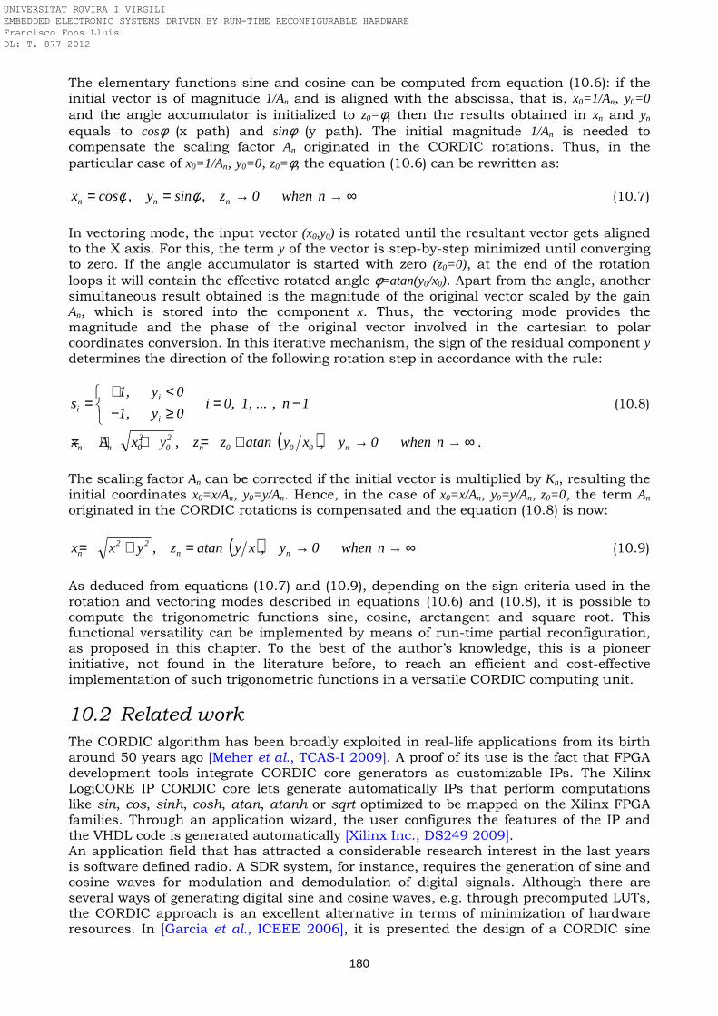
180
The elementary functions sine and cosine can be computed from equation (10.6): if the initial vector is of magnitude 1/An and is aligned with the abscissa, that is, x0=1/An, y0=0 and the angle accumulator is initialized to z0=φ, then the results obtained in xn and yn equals to cosφ (x path) and sinφ (y path). The initial magnitude 1/An is needed to compensate the scaling factor An originated in the CORDIC rotations. Thus, in the particular case of x0=1/An, y0=0, z0=φ, the equation (10.6) can be rewritten as:
∞→→== nwhen0zsinycosx nnn ,, φφ (10.7)
In vectoring mode, the input vector (x0,y0) is rotated until the resultant vector gets aligned to the X axis. For this, the term y of the vector is step-by-step minimized until converging to zero. If the angle accumulator is started with zero (z0=0), at the end of the rotation loops it will contain the effective rotated angle φ=atan(y0/x0). Apart from the angle, another simultaneous result obtained is the magnitude of the original vector scaled by the gain An, which is stored into the component x. Thus, the vectoring mode provides the magnitude and the phase of the original vector involved in the cartesian to polar coordinates conversion. In this iterative mechanism, the sign of the residual component y determines the direction of the following rotation step in accordance with the rule:
−=≥−<+
= 1n...1,0,i0y1,
0y1,s
i
i
i , (10.8)
( ) ∞→→+=+⋅= nwhen0yxyatanzzyxAx n000n20
20nn ,, .
The scaling factor An can be corrected if the initial vector is multiplied by Kn, resulting the initial coordinates x0=x/An, y0=y/An. Hence, in the case of x0=x/An, y0=y/An, z0=0, the term An originated in the CORDIC rotations is compensated and the equation (10.8) is now:
( ) ∞→→=+= nwhen0yxyatanzyxx nn22
n ,, (10.9)
As deduced from equations (10.7) and (10.9), depending on the sign criteria used in the rotation and vectoring modes described in equations (10.6) and (10.8), it is possible to compute the trigonometric functions sine, cosine, arctangent and square root. This functional versatility can be implemented by means of run-time partial reconfiguration, as proposed in this chapter. To the best of the author’s knowledge, this is a pioneer initiative, not found in the literature before, to reach an efficient and cost-effective implementation of such trigonometric functions in a versatile CORDIC computing unit.
10.2 Related work
The CORDIC algorithm has been broadly exploited in real-life applications from its birth around 50 years ago [Meher et al., TCAS-I 2009]. A proof of its use is the fact that FPGA development tools integrate CORDIC core generators as customizable IPs. The Xilinx LogiCORE IP CORDIC core lets generate automatically IPs that perform computations like sin, cos, sinh, cosh, atan, atanh or sqrt optimized to be mapped on the Xilinx FPGA families. Through an application wizard, the user configures the features of the IP and the VHDL code is generated automatically [Xilinx Inc., DS249 2009]. An application field that has attracted a considerable research interest in the last years is software defined radio. A SDR system, for instance, requires the generation of sine and cosine waves for modulation and demodulation of digital signals. Although there are several ways of generating digital sine and cosine waves, e.g. through precomputed LUTs, the CORDIC approach is an excellent alternative in terms of minimization of hardware resources. In [Garcia et al., ICEEE 2006], it is presented the design of a CORDIC sine
UNIVERSITAT ROVIRA I VIRGILI EMBEDDED ELECTRONIC SYSTEMS DRIVEN BY RUN-TIME RECONFIGURABLE HARDWARE Francisco Fons Lluís DL: T. 877-2012
181
and cosine wave generator. It is proposed a pipelined implementation of the CORDIC algorithm working in rotation mode to provide an output sample at every clock cycle. The full design is targeted into a Spartan-3 XC3S200-5FT256 device and it is synthesized in two ways: speed optimization and area optimization. In speed optimization, the maximum frequency of operation is estimated in 154.69 MHz and the resources used are 1104 slices, 615 flip-flops, 1748 4-input LUTs and 43 IOBs. In area optimization, the maximum frequency remains at 124.67 MHz and the resources involved are 1075 slices, 570 flip-flops, 1737 4-input LUTs and 43 IOBs. Vachhani et al. propose two CORDIC algorithms with an angular resolution of 1º [Vachhani et al., TCAS-II 2009]. The two architectures are mapped on a Xilinx Spartan XC2S200E FPGA device. The first one eliminates the use of ROM and requires 3 adders-substractors. It occupies 186 slices decomposed in 350 LUTs and 97 flip-flops/latches. The second one eliminates the use of barrel shifters and requires 2 adders-substractors and a ROM. It is composed of 203 slices with a total of 378 LUTs and 73 flip-flops/latches. Both algorithms require 10 iterations in the worst case to converge within 1º, although they take 7 or fewer iterations for about the 80% of the angles. The operation frequency is 54.35 MHz for the first algorithm and 60.80 MHz for the second. In [Adiono and Saut, ICEEI 2009], it is presented a pipelined datapath architecture of a 14-iteration CORDIC computer on an Altera Cyclone-II EP2C35F672C6N FPGA device. It operates with 16-bit fixed point data reaching an error of 0.058533 and 0.060059 for the X and Y components, while no error is obtained in the angle. Synthesis results show that the design fits in the 9% of the total logic elements of the FPGA and runs at 81.31 MHz. The implementation approaches seen up to now are based on conventional radix-2 CORDIC architectures. The development of high-radix CORDIC algorithm arises as a valid alternative intended for reducing the number of iterations, i.e., CORDIC calculation latency, with a reasonable increment of hardware complexity in high-speed applications. With the increment of radix, the number of iterations for a given precision is reduced, resulting in a potentially faster execution. In [Bhattacharyya et al., MICPRO 2010], it is proposed a radix-4 CORDIC processor implemented in a Xilinx XCV1000-6BG560 FPGA. The latency of the architecture is n/2 clock cycles and the throughput rate is one valid result per n/2 clocks for n bit precision. Thus, a 16-bit radix-4 CORDIC is implemented with the corresponding latency of eight clock cycles. It occupies 797 slices, 1554 LUTs, 85 flip-flops and 118 IOBs and operates at 56.96 MHz. All the related works introduced above are implemented in FPGA devices giving rise to a static hardware design. To the best of the author’s knowledge, the CORDIC implementation proposed in this chapter is the first one in the scientific literature that exploits the run-time reconfigurable features of modern FPGA devices. After this approach, other works conducted by the research community have appeared that implement a CORDIC processor able to be reconfigured on the fly, some of them inspired in part by the work presented in this chapter. Thus, Wang et al. present a CORDIC core mapped on a dynamically reconfigurable FPGA device oriented to a multiple input multiple output (MIMO) square root decoder for wireless applications [Wang et al., IPDPS 2007], [Wang et al., ICC 2008]. Similarly, Jianwen and Chuen propose a partially reconfigurable FPGA platform for computing the matrix inversion operation based on a run-time reconfigurable CORDIC computer [Jianwen and Ching, ISIC 2007]. The next section describes two implementation approaches of a trigonometric CORDIC computer implemented in two comercial run-time self-reconfigurable FPGA platforms.
10.3 Run-time reconfigurable hardware implementation
Despite the habitual trend of implementing signal processing algorithms through DSPs or GPPs, the CORDIC algorithm is optimized through dedicated hardware owing to its potential customizable parallelism and other reasons listed next [Andraka, FPGA 1998]: The algorithm presents an iterative mechanism easily synthesizable in an FPGA. Many
of the involved elementary functions such as trigonometric, exponential and
UNIVERSITAT ROVIRA I VIRGILI EMBEDDED ELECTRONIC SYSTEMS DRIVEN BY RUN-TIME RECONFIGURABLE HARDWARE Francisco Fons Lluís DL: T. 877-2012
182
logarithmic operations, on the contrary, cannot be efficiently evaluated with multiply-accumulate (MAC) units present in DSP processors. Consequently, whenever algorithms incorporate these functions, it is not unusual to observe significant performance degradation.
The accuracy of the result depends basically on the number of iterations done by the algorithm and the data size of the operands involved in the computations. This characteristic demands to increase the word width to the necessary length in accordance with the desirable precision, and this fact, unlike the microprocessor architecture, can be customized in an ASIC or FPGA. In an MCU, computations involving operands or data length longer than the MCU word penalize dramatically the system performance achievable in software.
Additionally, a relevant characteristic is noticed from the theoretical study shown above: the difference between the sine/cosine and the arctangent/magnitude functions is found only in the sign criterion, given that the three CORDIC equations (10.4) remain invariable in both rotation and vectoring modes. This fact inspires the author to perform a CORDIC implementation under a SoC/FPGA device based on partial reconfiguration: the computing unit is partitioned in a static circuitry or hardware skeleton that remains unchanged and a dynamically reconfigurable block that can evolve at run-time depending on the mathematic function to compute. Another idea exploited in this chapter consists in synthesizing specific trigonometric computers that are downloaded into a PR region of the FPGA when required and are switched with other computers or coprocessors executed multiplexed in time in the PRR while the application progresses. These concepts are explored in detail in the next sections.
10.3.1 Hardware/Software co-design and run-time reconfiguration
This chapter evaluates the implementation of a radix-2 CORDIC-based trigonometric computer on different platforms attending to the reconfiguration granularity of the FPGA device in use. Two implementation approaches are presented: On the one hand, it is proposed the implementation of a general-purpose trigonometric
computer that allows synthesizing different trigonometric functions under a fixed architectural skeleton provided with some reconfigurable modules which via dynamic reconfiguration can switch among different trigonometric functions. This fine-grain reconfiguration solution is conducted in an Atmel AT94K FPSLIC and permits to perfom operations like sin(φ), cos(φ), atan(y,x) and sqrt(x2+y2).
On the other hand, a second approach is proposed aimed at integrating a specific trigonometric computer responsible for the atan(y,x) function implemented in a Xilinx Virtex-4 FPGA in accordance with the general-purpose system architecture proposed in chapter 4. This second alternative, unlike the fine-grain approach in FPSLIC, corresponds to a coarse-grain reconfiguration alternative where the trigonometric computer is instantiated in a PRR when required. Once such computation is finished, the application can decide to replace the current trigonometric computer by another specific coprocessor in the PRR. In this option, the reconfiguration of the CORDIC processor is conducted as a whole.
These two CORDIC implementation approaches are detailed in sections 10.4 and 10.5.
10.4 Unified fine-grain reconfigurable implementation
The chosen platform is the Atmel AT94K40 especially due to its single-chip architecture composed of an 8-bit AVR MCU and an AT40K40 FPGA and its fine configuration granularity, supporting full and partial dynamic reconfiguration. The entire device or selected portions can be reconfigured at run-time by the MCU or the FPGA itself through the internal configuration controller. In this way, MCU and FPGA work seamlessly in computing elementary functions of the trigonometric CORDIC algorithm such as sin(z0), cos(z0), atan(y0/x0) and magn(y0,x0). The API or function prototypes are described next.
UNIVERSITAT ROVIRA I VIRGILI EMBEDDED ELECTRONIC SYSTEMS DRIVEN BY RUN-TIME RECONFIGURABLE HARDWARE Francisco Fons Lluís DL: T. 877-2012
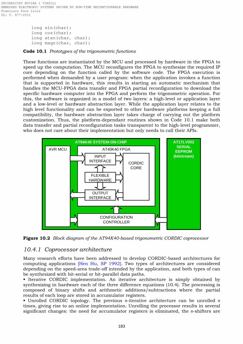
183
long sin(char); long cos(char); long atan(char, char); long magn(char, char);
Code 10.1 Prototypes of the trigonometric functions These functions are instantiated by the MCU and processed by hardware in the FPGA to speed up the computation. The MCU reconfigures the FPGA to synthesize the required IP core depending on the function called by the software code. The FPGA execution is performed when demanded by a user program: when the application invokes a function that is supported in hardware, this results in starting an automatic mechanism that handles the MCU-FPGA data transfer and FPGA partial reconfiguration to download the specific hardware computer into the FPGA and perform the trigonometric operation. For this, the software is organized in a model of two layers: a high-level or application layer and a low-level or hardware abstraction layer. While the application layer relates to the high level functionality and can be exported to other hardware platforms keeping a full compatibility, the hardware abstraction layer takes charge of carrying out the platform customization. Thus, the platform-dependant routines shown in Code 10.1 make both data transfer and partial reconfiguration tasks transparent to the high-level programmer, who does not care about their implementation but only needs to call their APIs.
AT94K40 SYSTEM-ON-CHIP
AT40K40 FPGAAVR MCU
AT17LV002SERIAL
EEPROM(bitstream)
CORDICCORE
INPUTINTERFACE
OUTPUTINTERFACE
FLEXIBLEHARDWARE
CONFIGURATIONCONTROLLER
AT94K40 SYSTEM-ON-CHIP
AT40K40 FPGAAVR MCU
AT17LV002SERIAL
EEPROM(bitstream)
CORDICCORE
INPUTINTERFACE
OUTPUTINTERFACE
FLEXIBLEHARDWARE
CONFIGURATIONCONTROLLER
Figure 10.2 Block diagram of the AT94K40-based trigonometric CORDIC coprocessor
10.4.1 Coprocessor architecture
Many research efforts have been addressed to develop CORDIC-based architectures for computing applications [Hen Hu, SP 1992]. Two types of architectures are considered depending on the speed-area trade-off intended by the application, and both types of can be synthesized with bit-serial or bit-parallel data paths. Iterative CORDIC implementation. An iterative architecture is simply obtained by synthesizing in hardware each of the three difference equations (10.4). The processing is composed of binary shifts and arithmetic additions/subtractions where the partial results of each loop are stored in accumulator registers. Unrolled CORDIC topology. The previous n-iterative architecture can be unrolled n times, giving rise to an online implementation. Unrolling the processor results in several significant changes: the need for accumulator registers is eliminated, the n-shifters are
UNIVERSITAT ROVIRA I VIRGILI EMBEDDED ELECTRONIC SYSTEMS DRIVEN BY RUN-TIME RECONFIGURABLE HARDWARE Francisco Fons Lluís DL: T. 877-2012
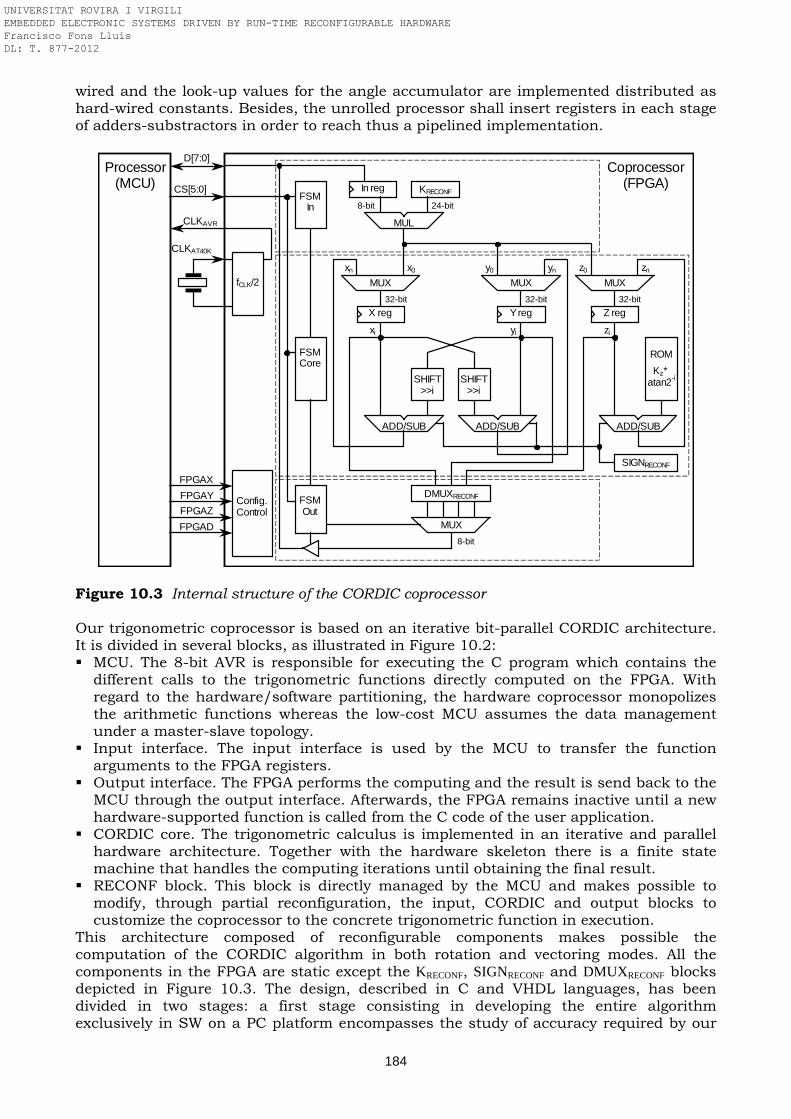
184
wired and the look-up values for the angle accumulator are implemented distributed as hard-wired constants. Besides, the unrolled processor shall insert registers in each stage of adders-substractors in order to reach thus a pipelined implementation.
Figure 10.3 Internal structure of the CORDIC coprocessor Our trigonometric coprocessor is based on an iterative bit-parallel CORDIC architecture. It is divided in several blocks, as illustrated in Figure 10.2: MCU. The 8-bit AVR is responsible for executing the C program which contains the
different calls to the trigonometric functions directly computed on the FPGA. With regard to the hardware/software partitioning, the hardware coprocessor monopolizes the arithmetic functions whereas the low-cost MCU assumes the data management under a master-slave topology.
Input interface. The input interface is used by the MCU to transfer the function arguments to the FPGA registers.
Output interface. The FPGA performs the computing and the result is send back to the MCU through the output interface. Afterwards, the FPGA remains inactive until a new hardware-supported function is called from the C code of the user application.
CORDIC core. The trigonometric calculus is implemented in an iterative and parallel hardware architecture. Together with the hardware skeleton there is a finite state machine that handles the computing iterations until obtaining the final result.
RECONF block. This block is directly managed by the MCU and makes possible to modify, through partial reconfiguration, the input, CORDIC and output blocks to customize the coprocessor to the concrete trigonometric function in execution.
This architecture composed of reconfigurable components makes possible the computation of the CORDIC algorithm in both rotation and vectoring modes. All the components in the FPGA are static except the KRECONF, SIGNRECONF and DMUXRECONF blocks depicted in Figure 10.3. The design, described in C and VHDL languages, has been divided in two stages: a first stage consisting in developing the entire algorithm exclusively in SW on a PC platform encompasses the study of accuracy required by our
KRECONF In reg
Processor (MCU)
Coprocessor (FPGA)
FPGAX
FPGAY
FPGAZ
FPGAD
D[7:0]
CS[5:0]
CLKAVR
x0
xn
yn
yi
zn
zi
xi
z0
y0
MUL
ADD/SUB
ADD/SUB
ADD/SUB
SIGNRECONF
DMUXRECONF
ROM
Kz∗ atan2-i
MUX
MUX
MUX
MUX
Config. Control
FSM In
SHIFT >>i
SHIFT >>i
CLKAT40K
FSM Core
FSM Out
Y reg
fCLK/2
Z reg X reg
8-bit
24-bit
32-bit
32-bit
32-bit
8-bit
UNIVERSITAT ROVIRA I VIRGILI EMBEDDED ELECTRONIC SYSTEMS DRIVEN BY RUN-TIME RECONFIGURABLE HARDWARE Francisco Fons Lluís DL: T. 877-2012
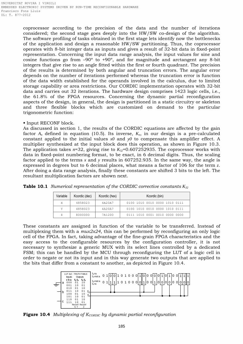
185
coprocessor according to the precision of the data and the number of iterations considered; the second stage goes deeply into the HW/SW co-design of the algorithm. The software profiling of tasks obtained in the first stage lets identify now the bottlenecks of the application and design a reasonable HW/SW partitioning. Thus, the coprocessor operates with 8-bit integer data as inputs and gives a result of 32-bit data in fixed-point representation. Concerning the input data range analysis, the input values for sine and cosine functions go from –90º to +90º, and for magnitude and arctangent any 8-bit integers that give rise to an angle fitted within the first or fourth quadrant. The precision of the results is determined by both angular and truncation errors. The angular error depends on the number of iterations performed whereas the truncation error is function of the data width established for the operands involved in the calculus, due to limited storage capability or area restrictions. Our CORDIC implementation operates with 32-bit data and carries out 32 iterations. The hardware design comprises 1423 logic cells, i.e., the 61.8% of the FPGA resources. Concerning the dynamic partial reconfiguration aspects of the design, in general, the design is partitioned in a static circuitry or skeleton and three flexible blocks which are customized on demand to the particular trigonometric function: Input RECONF block. As discussed in section 1, the results of the CORDIC equations are affected by the gain factor An defined in equation (10.5). Its inverse, Kn, in our design is a pre-calculated constant applied to the initial values x0 and y0 to compensate this amplifier effect. A multiplier synthesized at the input block does this operation, as shown in Figure 10.3. The application takes n=32, giving rise to K32=0.607252935. The coprocessor works with data in fixed-point numbering format, to be exact, in 6 decimal digits. Thus, the scaling factor applied to the terms x and y results in 607252.935. In the same way, the angle is expressed in degrees but to 6 decimal places, what means a factor of 106 for the term z. After doing a data range analysis, finally these constants are shifted 3 bits to the left. The resultant multiplication factors are shown next. Table 10.1 Numerical representation of the CORDIC corrective constants K32
Variable Kcordic (dec) Kcordic (hex) Kcordic (bin)
X 4858023 4A20A7 0100 1010 0010 0000 1010 0111
Y 4858023 4A20A7 0100 1010 0010 0000 1010 0111
Z 8000000 7A1200 0111 1010 0001 0010 0000 0000
These constants are assigned in function of the variable to be transferred. Instead of multiplexing them with a mux2x24, this can be performed by reconfiguring an only logic cell of the FPGA. In fact, taking advantage of the fine-grain FPGA characteristics and the easy access to the configurable resources by the configuration controller, it is not necessary to synthesize a generic MUX with its select lines controlled by a dedicated FSM; this can be handled by the MCU through reconfiguring the LUT of a logic cell in order to negate or not its input and in this way generate two outputs that are applied to the bits that differ from a constant to another, as depicted in Figure 10.4.
Figure 10.4 Multiplexing of KCORDIC by dynamic partial reconfiguration
LUT 3x2 - TRUTH TABLE 0
1
0
0
1
0
0
0
1
0
0
0
0
0
0
0
1
1
0
1
0
1
1
1
0
0
1
1
0
0
0
0
0
0
1
0
0
1
0
0
0
0
fG=a fH=not a
fG=not a fH=a
a
b
c
fG
fH
Inputs Outputs c b a fG fH fG fH
0 0 0 0 1 1 0 0 0 1 1 0 0 1 0 1 0 0 1 1 0 0 1 1 1 0 0 1 1 0 0 0 1 1 0 1 0 1 1 0 0 1 1 1 0 0 1 1 0 1 1 1 1 0 0 1
Reconf Reconf X, Y Z
1
0
1
0
1
0
UNIVERSITAT ROVIRA I VIRGILI EMBEDDED ELECTRONIC SYSTEMS DRIVEN BY RUN-TIME RECONFIGURABLE HARDWARE Francisco Fons Lluís DL: T. 877-2012
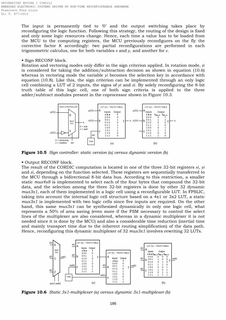
186
The input is permanently tied to ‘0’ and the output switching takes place by reconfiguring the logic function. Following this strategy, the routing of the design is fixed and only some logic resources change. Hence, each time a value has to be loaded from the MCU to the computing registers, the MCU previously reconfigures on the fly the corrective factor K accordingly: two partial reconfigurations are performed in each trigonometric calculus, one for both variables x and y, and another for z. Sign RECONF block. Rotation and vectoring modes only differ in the sign criterion applied. In rotation mode, zi is considered for taking the addition/subtraction decision as shown in equation (10.6) whereas in vectoring mode the variable yi becomes the selection key in accordance with equation (10.8). Like this, the sign criterion can be implemented through an only logic cell combining a LUT of 2 inputs, the signs of yi and zi. By solely reconfiguring the 8-bit truth table of this logic cell, one of both sign criteria is applied to the three adder/subtract modules present in the coprocessor shown in Figure 10.3.
Figure 10.5 Sign controller: static version (a) versus dynamic version (b) Output RECONF block. The result of the CORDIC computation is located in one of the three 32-bit registers xi, yi and zi, depending on the function selected. These registers are sequentially transferred to the MCU through a bidirectional 8-bit data bus. According to this restriction, a smaller static mux4x8 is implemented to select each of the four bytes that compound the 32-bit data, and the selection among the three 32-bit registers is done by other 32 dynamic mux3x1, each of them implemented in a logic cell using a reconfigurable LUT. In FPSLIC, taking into account the internal logic cell structure based on a 4x1 or 3x2 LUT, a static mux3x1 is implemented with two logic cells since five inputs are required. On the other hand, this same mux3x1 can be synthesized dynamically in only one logic cell, what represents a 50% of area saving (even more if the FSM necessary to control the select lines of the multiplexer are also considered, whereas in a dynamic multiplexer it is not needed since it is done by the MCU) and also a considerable time reduction (inertial time and mainly transport time due to the inherent routing simplification) of the data path. Hence, reconfiguring this dynamic multiplexer of 32 mux3x1 involves rewriting 32 LUTs.
Figure 10.6 Static 3x1-multiplexer (a) versus dynamic 3x1-multiplexer (b)
sel
yi(31)
(a) (b)
LUT 3x1 – TRUTH TABLE
a
b
c
f
Inputs Output c b a f
0 0 0 0 0 0 1 1 0 1 0 0 0 1 1 1 1 0 0 1 1 0 1 1 1 1 0 0 1 1 1 0
zi(31)
sel
si
yi(31)
LUT 3x1 – TRUTH TABLE
a
b
c
f
Inputs Output c b a fSEL=0 fSEL=1
0 0 0 0 1 0 0 1 1 1 0 1 0 0 0 0 1 1 1 0 1 0 0 0 1 1 0 1 1 1 1 1 0 0 0 1 1 1 1 0
zi(31)
si
FSM
zi(31)
yi(31)
MUX 2x1
0 = vectoring 1 = rotation
0
1
SIGN CONTROLLER
0 = sub 1 = add
si
x(i)
(a) (b)
LUT 3x1 – TRUTH TABLE
a
b
c
f
Inputs Output c b a f
0 0 0 0 0 0 1 1 0 1 0 0 0 1 1 1 1 0 0 0 1 0 1 0 1 1 0 1 1 1 1 1
y(i)
sel(0)
LUT 3x1 – TRUTH TABLE
a
b
c
f
z(i)
FSM
z(i)
x(i)
out(i)
MUX 3x1
sel(1) sel(0)
0
1
2
y(i)
x(i)
LUT 3x1 – TRUTH TABLE
a
b
c
f
Inputs Output c b a fSEL=0 fSEL=1 fSEL=2
0 0 0 0 0 0 0 0 1 1 0 0 0 1 0 0 1 0 0 1 1 1 1 0 1 0 0 0 0 1 1 0 1 1 0 1 1 1 0 0 1 1 1 1 1 1 1 1
y(i)
sel(1)
Inputs Output c b a f
0 0 0 0 0 0 1 1 0 1 0 0 0 1 1 1 1 0 0 0 1 0 1 0 1 1 0 1 1 1 1 1
out(i)
out(i)
z(i)
UNIVERSITAT ROVIRA I VIRGILI EMBEDDED ELECTRONIC SYSTEMS DRIVEN BY RUN-TIME RECONFIGURABLE HARDWARE Francisco Fons Lluís DL: T. 877-2012
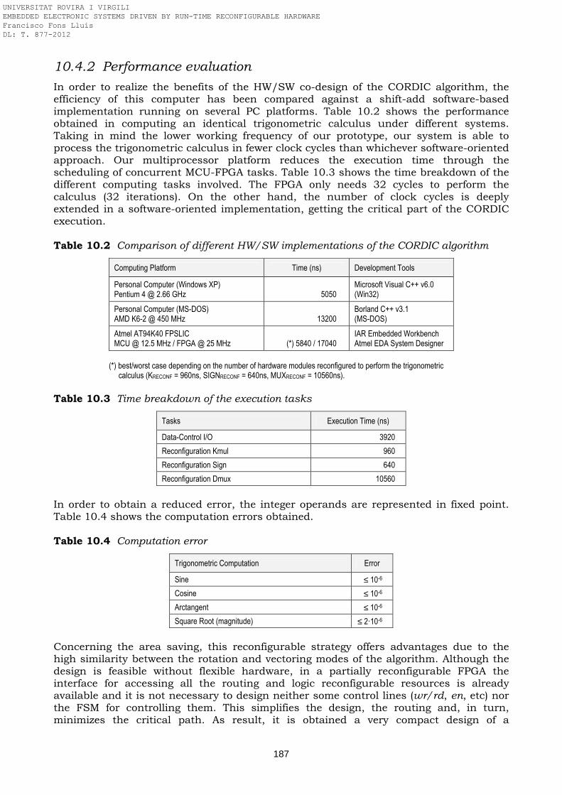
187
10.4.2 Performance evaluation
In order to realize the benefits of the HW/SW co-design of the CORDIC algorithm, the efficiency of this computer has been compared against a shift-add software-based implementation running on several PC platforms. Table 10.2 shows the performance obtained in computing an identical trigonometric calculus under different systems. Taking in mind the lower working frequency of our prototype, our system is able to process the trigonometric calculus in fewer clock cycles than whichever software-oriented approach. Our multiprocessor platform reduces the execution time through the scheduling of concurrent MCU-FPGA tasks. Table 10.3 shows the time breakdown of the different computing tasks involved. The FPGA only needs 32 cycles to perform the calculus (32 iterations). On the other hand, the number of clock cycles is deeply extended in a software-oriented implementation, getting the critical part of the CORDIC execution. Table 10.2 Comparison of different HW/SW implementations of the CORDIC algorithm
Computing Platform Time (ns) Development Tools
Personal Computer (Windows XP) Pentium 4 @ 2.66 GHz
5050
Microsoft Visual C++ v6.0 (Win32)
Personal Computer (MS-DOS) AMD K6-2 @ 450 MHz
13200
Borland C++ v3.1 (MS-DOS)
Atmel AT94K40 FPSLIC MCU @ 12.5 MHz / FPGA @ 25 MHz
(*) 5840 / 17040
IAR Embedded Workbench Atmel EDA System Designer
(*) best/worst case depending on the number of hardware modules reconfigured to perform the trigonometric calculus (KRECONF = 960ns, SIGNRECONF = 640ns, MUXRECONF = 10560ns).
Table 10.3 Time breakdown of the execution tasks
Tasks Execution Time (ns)
Data-Control I/O 3920
Reconfiguration Kmul 960
Reconfiguration Sign 640
Reconfiguration Dmux 10560
In order to obtain a reduced error, the integer operands are represented in fixed point. Table 10.4 shows the computation errors obtained. Table 10.4 Computation error
Trigonometric Computation Error
Sine ≤ 10-6
Cosine ≤ 10-6
Arctangent ≤ 10-6
Square Root (magnitude) ≤ 210-6
Concerning the area saving, this reconfigurable strategy offers advantages due to the high similarity between the rotation and vectoring modes of the algorithm. Although the design is feasible without flexible hardware, in a partially reconfigurable FPGA the interface for accessing all the routing and logic reconfigurable resources is already available and it is not necessary to design neither some control lines (wr/rd, en, etc) nor the FSM for controlling them. This simplifies the design, the routing and, in turn, minimizes the critical path. As result, it is obtained a very compact design of a
UNIVERSITAT ROVIRA I VIRGILI EMBEDDED ELECTRONIC SYSTEMS DRIVEN BY RUN-TIME RECONFIGURABLE HARDWARE Francisco Fons Lluís DL: T. 877-2012
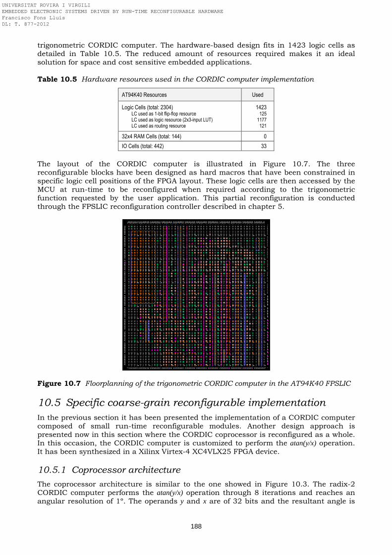
188
trigonometric CORDIC computer. The hardware-based design fits in 1423 logic cells as detailed in Table 10.5. The reduced amount of resources required makes it an ideal solution for space and cost sensitive embedded applications. Table 10.5 Hardware resources used in the CORDIC computer implementation
AT94K40 Resources Used
Logic Cells (total: 2304) LC used as 1-bit flip-flop resource LC used as logic resource (2x3-input LUT) LC used as routing resource
1423 125
1177 121
32x4 RAM Cells (total: 144) 0
IO Cells (total: 442) 33
The layout of the CORDIC computer is illustrated in Figure 10.7. The three reconfigurable blocks have been designed as hard macros that have been constrained in specific logic cell positions of the FPGA layout. These logic cells are then accessed by the MCU at run-time to be reconfigured when required according to the trigonometric function requested by the user application. This partial reconfiguration is conducted through the FPSLIC reconfiguration controller described in chapter 5.
Figure 10.7 Floorplanning of the trigonometric CORDIC computer in the AT94K40 FPSLIC
10.5 Specific coarse-grain reconfigurable implementation
In the previous section it has been presented the implementation of a CORDIC computer composed of small run-time reconfigurable modules. Another design approach is presented now in this section where the CORDIC coprocessor is reconfigured as a whole. In this occasion, the CORDIC computer is customized to perform the atan(y/x) operation. It has been synthesized in a Xilinx Virtex-4 XC4VLX25 FPGA device.
10.5.1 Coprocessor architecture
The coprocessor architecture is similar to the one showed in Figure 10.3. The radix-2 CORDIC computer performs the atan(y/x) operation through 8 iterations and reaches an angular resolution of 1º. The operands y and x are of 32 bits and the resultant angle is
UNIVERSITAT ROVIRA I VIRGILI EMBEDDED ELECTRONIC SYSTEMS DRIVEN BY RUN-TIME RECONFIGURABLE HARDWARE Francisco Fons Lluís DL: T. 877-2012
189
delivered in 32-bit format. The reconfigurable components used in Figure 10.3 are not required now since the computer is architected to work only in vectoring mode. In this approach, the trigonometric computer becomes a coprocessor that is instantiated in the PR region of the standard and minimalist reconfigurable system architecture presented in chapter 4 (in section 4.4.1, Figure 4.4). Therefore, the whole CORDIC coprocessor is downloaded in the PRR when the application flow managed in software requires computing the arctangent function. Following the same application flow than in the FPSLIC solution, here the MicroBlaze processor takes charge of transferring the operands to the PRR and reading the computation result. Once this computation is performed, the application can decide to download new coprocessors in the PRR since this region is used as a time-shared resource.
10.5.2 Performance evaluation
The resources involved in the synthesis of this coprocessor placed in the PRR are shown next in Table 10.6. In this occasion, the microprocessor runs at 100 MHz whereas the coprocessor placed in the PRR works at 50 MHz. Since the computation of the arctangent is performed in 8 iterations and each iteration is performed in one clock, an output angle is obtained each 160 ns. Table 10.6 Hardware resources used in the CORDIC atan(y/x) computer implementation
XC4VLX25 Resources Used
Slices (total: 10752) 529
1-bit flip-flop (total: 21504) 284
4-input LUT (total: 21504) 945
18-kbit RAMB16 block (total: 72) 0
DSP48 block (total: 48) 0
Bonded IOBs (total: 448) 0
10.6 Summary
The beauty of CORDIC lies in the fact that by simple shift-add operations, it can perform several computing tasks such as trigonometric, hyperbolic and logarithmic functions, real and complex multiplications, divisions, square roots and many others. Moreover, accurate computations can be performed in hardware-efficient implementations without employing time- and area-consuming divisions and floating-point calculations. Taking into account the inherent flexibility of the CORDIC algorithm to implement different types of computations, this work describes the design of a dynamically reconfigurable trigonometric coprocessor mapped in two different SoC/FPGA platforms where, while a low-cost CPU runs the program flow, a hardware coprocessor takes charge of the computing. Two implementation approaches are explored: fine-grain reconfiguration, where the design pursues to optimize the placement and routing of the computer by reconfiguring on the fly only specific LUT-based blocks, and coarse-grain reconfiguration, where the CORDIC coprocessor –treated as an IP core– is reconfigured as a whole in a specific PR region of the FPGA when that specific trigonometric computation is required by the application. The concept reached is a single-chip cost-effective embedded system that just running at a low frequency perfoms sine, cosine, arctangent and square root operations at rates comparable to PC platform. The proof-of-feasibility conducted in this work demonstrates that PR is a powerful technology with an enormous potential that can dramatically extend the capabilities of programmable logic devices. The system architecture presented is specially suited to cost-sensitive time-critical embedded applications.
UNIVERSITAT ROVIRA I VIRGILI EMBEDDED ELECTRONIC SYSTEMS DRIVEN BY RUN-TIME RECONFIGURABLE HARDWARE Francisco Fons Lluís DL: T. 877-2012
190
References
[Adiono and Saut, ICEEI 2009] T. Adiono, R. Saut Purba, Scalable pipelined CORDIC architecture design and implementation in FPGA, Proc. of the International Conference on Electrical Engineering and Informatics, pp. 646-649, 2009.
[Andraka, FPGA 1998] R. Andraka, A survey of CORDIC algorithms for FPGA based computers, Proceedings of the ACM/SIGDA International Symposium on Field Programmable Gate Arrays, pp.191-200, 1998.
[Angarita et al., FPL 2005] F. Angarita, A. Perez-Pascual, T. Sansaloni, J. Valls, Efficient FPGA implementation of CORDIC algorithm for circular and linear coordinates, Proc. Int. Conf. on Field Programmable Logic and Applications, pp. 535-538, 2005.
[Bhattacharyya et al., MICPRO 2010] K. Bhattacharyya, R. Biswas, A.S. Dhar, S. Banerjee, Architectural design and FPGA implementation of radix-4 CORDIC processor, Microprocessor and Microsystems, vol. 34, no.2-4, pp. 96-101, 2010.
[Garcia et al., ICEEE 2006] E.O. Garcia, R. Cumplido, M. Arias, Pipelined CORDIC design on FPGA for a digital sine and cosine waves generator, Proc. of the Int. Conf. on Electrical and Electronics Engineering, pp. 104-107, 2006.
[Hen Hu, SP 1992] Y. Hen Hu, CORDIC-based VLSI architectures for digital signal processing, IEEE Signal Processing Magazine, pp.16-35, 1992.
[Jianwen and Ching, ISIC 2007] L. Jianwen, J. Ching Chuen, A System-on-Chip dynamically reconfigurable FPGA platform for matrix inversion, Proceedings of the IEEE International Symposium on Integrated Circuits, pp. 465-468, 2007.
[Meher et al., TCAS-I 2009] P.K. Meher, J. Valls, T.B. Juang, K. Sridharan, K. Maharatna, 50 years of CORDIC: algorithms, architectures, and applications, IEEE Trans. of Circuits and Systems I, vol. 56, no. 9, pp. 1893-1907, 2009.
[Timmermann et al., JSSC 1991] D. Timmermann, H. Hahn, B.J. Hosticka, G. Schimdt, A programmable CORDIC chip for digital signal processing applications, IEEE Journal of Solid-State Circuits, vol. 26, no. 9, pp. 1317-1321, 1991.
[Vachhani et al., TCAS-II 2009] L. Vachhani, K. Sridharan, P.K. Meher, Efficient CORDIC algorithms and architectures for low area and high throughput implementation, IEEE Trans. on Circuits and Systems II, vol. 56, no. 1, pp. 61-65, 2009.
[Vachhani et al., TIE 2009] L. Vachhani, K. Sridharan, P.K. Meher, Efficient FPGA realization of CORDIC with application to robotic exploration, IEEE Transactions on Industrial Electronics, vol. 56, no. 12, pp. 4915-4929, 2009.
[Vladimirova and Tiggeler, MAPLD 1999] T. Vladimirova, H. Tiggeler, FPGA implementation of sine and cosine generators using the CORDIC algorithm, Proc. of Military & Aerospace Applications of Prog. Devices and Technologies Conf., 1999.
[Volder, IRETEC 1959] J.E. Volder, The CORDIC trigonometric computing technique, IRE Transactions on Electronic Computers, vol. EC-8, no. 3, pp. 330–334, 1959.
[Volder, VLSI 2000] J.E. Volder, The birth of CORDIC, Journal of VLSI Signal Processing, vol. 25, no. 2, pp. 101-105, 2000.
[Walther, SJCC 1971] J.S. Walther, A unified algorithm for elementary functions, Proceedings of Spring Joint Computer Conference, pp. 379–385, 1971.
[Walther, VLSI 2000] J.S. Walther, The story of unified CORDIC, Journal of VLSI Signal Processing, vol. 25, no. 2, pp. 107-112, 2000.
[Wang et al., ICC 2008] H. Wang, P. Leray, J. Palicot, An efficient MIMO V-BLAST decoder based on a dynamically reconfigurable FPGA including its reconfiguration management, Proc. IEEE Int. Conf. on Communications, pp. 746-750, 2008.
[Wang et al., IPDPS 2007] H. Wang, J.P. Delahaye, P. Leray, J. Palicot, Managing dynamic reconfiguration on MIMO decoder, Proc. of the IEEE International Parallel and Distributed Processing Symposium, pp. 1-8, 2007.
[Xilinx Inc., DS249 2009] Xilinx Inc., CORDIC v4.0, Datasheet 249, 2009.
UNIVERSITAT ROVIRA I VIRGILI EMBEDDED ELECTRONIC SYSTEMS DRIVEN BY RUN-TIME RECONFIGURABLE HARDWARE Francisco Fons Lluís DL: T. 877-2012
191
Chapter 11 Automatic fingerprint authentication system In the current era of communications and information technologies, embedded security is a feature highly demanded to systems that manage confidential, sensitive or critical data. More and more, our society needs secure applications which, as prerequisite, verify their users before authorizing them to access certain privileges stored there. It is not difficult to find real application examples in our daily lives; electronic tellers, computer networks, mobile phones or even automobiles are use cases that perform such authorization before granting access to the system. Under this context, many end-user applications that demand better levels of security than PINs, passwords or ID cards address personal recognition algorithms based on biometric (physiological or behavioral) characteristics. Today, automatic biometric-based personal recognition systems comprise high-performance signal- and image-processing applications with time-critical constraints, motivated especially by quality-of-service and ergonomic reasons. Moreover, biometric personal recognition is an appropriate example of compute-intensive algorithm decomposed in a series of processing tasks executed in a sequential order. The natural batch process observed in the execution of the biometric algorithm enables the use of run-time reconfiguration technology in an attempt to synthesize this application efficiently. In fact, as suggested in this chapter, run-time reconfigurable hardware technology brings key advantages in the design of automatic personal recognition systems, especially when oriented to consumer applications with stringent demands on real-time and low-cost. To the best of the author’s knowledge, this work is pioneer in regard to the introduction of run-time reconfigurable hardware to address the design and development of biometric recognition systems; although it is known the existence of biometric applications implemented in static hardware exploiting parallelism, e.g. on ASIC, ASSP or FPGA devices, this is probably the first time these applications are furthermore synthesized in hardware that evolves at run-time, aimed at sharing the available computational resources throughout the execution of mutually exclusive tasks of the application. The experimental results achieved prove it is possible to embed a full and highly demanding biometric recognition algorithm in a small electronic platform composed of a programmable logic device, processing such algorithm at real-time, preserving data accuracy and precision in the computation, and multiplexing functionality on the fly over a reduced set of physical resources reaching thus a low cost solution. Furthermore, the proven maturity experienced in this work regarding both run-time reconfiguration technology and EDA toolset supporting the design flow lets predict that the spread of this technology from research to industry is not far.
11.1 Introduction
Computationally complex applications processed in real-time, driven at low rates of power consumption and synthesized at low cost are unavoidable requirements today in the design and development of embedded systems, particularly when addressed to mass-production niches. Under this context, dynamic partial reconfiguration of SRAM-based FPGAs arises as a firm technological alternative, able to deliver a high functional density of resources to efficiently balance all those demands for time-, power- and cost-sensitive applications. Software-defined radio, aerospace missions and cryptography are some of the known applications that exploit the benefits of dynamic partial reconfiguration of programmable logic devices today. Following this line, this work applies now PR to a new application space that has not traditionally leveraged it: biometrics.
UNIVERSITAT ROVIRA I VIRGILI EMBEDDED ELECTRONIC SYSTEMS DRIVEN BY RUN-TIME RECONFIGURABLE HARDWARE Francisco Fons Lluís DL: T. 877-2012
192
There exist basically three methodologies for authenticating or identifying a user, depending on: something you have, for instance a key or an ID card; something you know, as a password or a PIN; and something you are – namely, biometrics. In spite of the three strategies available, the last one delivers the highest safety level against external attacks or frauds since biometric information, unlike keys or passwords, cannot be lost, stolen or forgotten. Hence, as security has become a major issue in today’s digital information environment, especially for application fields like e-commerce, ehealth, e-passports, e-banking or e-voting, among others, the author believes the use of PR in biometrics holds great promise. As humans, we all use our natural abilities to recognize people through their faces, fingerprints, voices and other genuine traits. Electronic systems, on the other hand, must be algorithmically instructed in how to use this same observable information to perform human recognition. Technological advances in the biometric field are helping to close the gap between human perception and machine recognition. A priority goal of using biometrics is to provide identity assurance –or the capability to accurately recognize individuals– with great reliability and speed, in addition to low cost. As a proof of concept in introducing run-time reconfigurable computing in high-performance applications, an automatic fingerprint authentication system (AFAS) has been implemented in two different programmable logic platforms: first in a SoPC composed of a hard-core MCU and an FPGA, and afterwards in a dynamically reconfigurable FPGA partitioned in a static region –which allocates a soft-core processor, some standard peripherals and a reconfiguration controller– and a partially reconfigurable region where different custom biometric IPs can be swapped in and out along the time. In both cases, all the tasks that compose the biometric algorithm are partitioned and synthesized first in a series of coprocessors that are then instantiated and executed multiplexed in time on the logic resources of the programmable logic device. Thus, the work conducted in this chapter presents the design of a full biometric recognition application driven by hardware/software co-design and reconfigurable hardware giving place to a collection of hardware IPs that are processed multiplexed in time in a set of shared resources in the programmable logic device.
11.1.1 Basics of biometrics
Biometric recognition systems offer automated methods for identity verification on the principle of measurable physiological or behavioral characteristics. Well-known personal biometric modalities include voice, face, gait, signature, fingerprint, iris, hand geometry, etc. From a commercial perspective, the market of biometric applications has gained significant attention in the last years: First, ensuring the safety of the citizens has become a major concern for most of our
governments. Besides, a great deal of IT applications such as e-commerce, e-banking and e-health
have triggered a real need for reliable, user-friendly, and widely acceptable control mechanisms for checking the identity of an individual.
Nowadays, fingerprint recognition is one of the biometric modalities most implanted in the society due to its acceptable identification rate, ease-of-use, ergonomics and efficiency in acquiring the biometric features, mainly oriented to silicon or optical (touchless) sensors, which let obtain a fingerprint image with good accuracy at an acceptable cost. Since long time ago, commercial products based on biometrics are available from different vendors and there exist many real application examples coming from official institutions all over the world that make use of fingerprint features, like the Federal Bureau of Investigation (FBI) or the US-Visit program from the U.S. Department of Homeland Security. Nevertheless, field deployment has raised many technical and non-technical issues which need to be tackled. Regarding embedded fingerprint-based recognition applications, basically two technical concerns are still open:
UNIVERSITAT ROVIRA I VIRGILI EMBEDDED ELECTRONIC SYSTEMS DRIVEN BY RUN-TIME RECONFIGURABLE HARDWARE Francisco Fons Lluís DL: T. 877-2012
193
On the one hand, the theoretical aspects applied to the recognition algorithm do not guarantee yet a free-of-errors authentication rate today. The last fingerprint verification competitions (FVC), conducted by both industry and academia, showed errors around 2.2% in both false acceptance and false rejection rates (FAR and FRR, respectively). The accuracy of the current state-of-the-art biometric recognition algorithms is still far from guaranteeing definitive levels of confidence. In this direction, a considerable research effort is still needed in signal and image processing in order to enhance the fingerprint recognition algorithms so that reduce those figures, aimed at providing a 100% of success in automatic machines to take the correct decision in authenticating/identifying a user. This fact would give even a major confidence to biometrics technology to extend its use in new potential application fields.
On the other hand, intimately related to the previous issue, the physical implementation of such biometric recognition algorithm in a cost-effective electronic platform and processed at acceptable ergonomic rates (i.e., performing the authentication/identification process at real-time, that usually means around 2 or 3 seconds) is today a really hard requirement only achievable through HPC platforms with prohibitive prices, fact that obstructs the deployment of such security level into certain cost-sensitive applications. Technological aspects focused on finding an electronic computing platform restricted in cost and compliant with the strict real-time specifications of the AFAS application are still non-solved, especially in embedded system domains addressed to manage medium or large fingerprint databases and perform the user identification in critical time. In this sense, increasing performance by lowering cost is one of the biggest technical issues that the developers of embedded AFAS face today.
This work concentrates its efforts in the second open issue mentioned above. However, biometrics, from a computational point of view, is complex. It requires stringent and computationally intensive image/signal processing in real-time, along with a great deal of flexibility. In addition, personal recognition algorithms are in continuous evolution. As the research community expends major effort in this field, error rates are decreasing. As a consequence, consumers are growing more confident about biometric systems, and acceptance is increasing. On the other hand, given that progress in biometrics technology is expected to continue in the future, biometric products already in the market will have to admit upgrades in the field just to avoid getting obsolete, and for this they require open system architectures. In this regard, the flexible hardware found in run-time reconfigurable FPGA devices meets the versatility and scalability needed. Moreover, cost-effectiveness is probably the most important reason for biometrics to make use of partial reconfigurability. In aggressive markets like consumer electronics or automotive, vendors must market their systems at a competitive cost. Customers demand products with the highest level of security at the lowest possible price point and the way to improve security and reliability is by increasing the computational power of the biometric recognition algorithm. This increment of computation usually involves a like increment in execution time and also in cost (resources). However, the cost is hardly affected in those scenarios where the design is based on dynamic-partial-reconfiguration technology. Using PR, designers can partition that new computation and schedule it as new processing stages added to the current sequential execution flow of the application. Thus, cost often can be held invariant to functional changes of the algorithm. Designers can partition the biometric recognition algorithm into a series of mutually exclusive stages that are processed sequentially, where the outputs or results of one stage become the input data for the next. This sequential order means designers can multiplex hardware resources in time and customize them to execute a different task or role at each moment, increasing their functional density and thus keeping constant the total number of resources needed to process the entire algorithm. Moreover, the reconfiguration overhead is short enough so as not to eclipse the benefits gained by hardware acceleration, and reconfiguring one set of resources on the fly will not interrupt
UNIVERSITAT ROVIRA I VIRGILI EMBEDDED ELECTRONIC SYSTEMS DRIVEN BY RUN-TIME RECONFIGURABLE HARDWARE Francisco Fons Lluís DL: T. 877-2012
194
the rest of the resources available in the FPGA. In this way, the resources that are not reconfigured continue to operate and guarantee the permanent link with the exterior world for the entire life cycle of the application. The challenge of this work consists in demonstrating that PR fits well in the development of complex personal recognition algorithms based on biometric characteristics, making use of a two-dimensional design abstraction level through which the functionality is managed not only in space but also in time. How the author emcompasses this target is described in the next sections.
11.1.2 Automatic fingerprint authentication system
Fingerprint verification is one of the most popular and reliable biometric techniques used in automatic personal recognition. Essentially, the technique splits the AFAS application in two processes or stages carried out at different times and in different conditions: enrollment and recognition. Enrollment is the system configuration process through which the user gets
registered. Generally, the user exposes his/her fingerprint to the system, which submits it to a set of computationally intensive image processing phases aimed at extracting all relevant, permanent and distinctive information that will permit the system to unequivocally recognize the fingerprint’s genuine owner. This set of characteristics becomes the user ID, which the system stores in its database. This process is normally conducted off-line, in a secure environment and under the guidance of expert staff.
Once the user is registered, the next time his/her fingerprint is exposed to the system in the recognition stage, the system will check if it corresponds with any authorized member within the database. All the processing tasks performed in the enrollment are repeated now to again extract those distinctive characteristics from the live fingerprint sample. The system then compares these characteristics with the information stored as user templates in the database to conclude whether the live scan matches any of the registered templates. Recognition comes in two modalities depending on the size of the database: authentication, when a one-to-one (or one-to-few) matching is processed; and identification, when the matching is one-to-many due to the fact that many users are registered in the system. Recognition is normally performed online in a less-secure environment and under real-time constraints.
Each of these stages is, in its turn, partitioned into a series of processing tasks designed to extract from the fingerprint image such information as will distinguish one user from the others. With that object in view, the system carries out specific computations, such as image processing (2D convolution, morphologic operations), trigonometrics (sin, cos, atan) or statistics (mean, variance).
11.2 Related work
In the arena of real-time secure media, cryptography and biometrics are two engineering fields intimately connected to each other, mainly due to several evident concerns: security is more and more demanded today; to deliver high levels of confidence it is required complex and compute-intensive processing; however, such computational demand shall not penalize in ergonomics, i.e., it must not impact on real-time performance of the end-user application. Like this, most applications that require the highest levels of security make use of these two closely related disciplines: on the one hand, the personal authentication/identification of a user becomes a necessary condition to grant access into a secure system and, on the other hand, in case this system needs to share some information with the exterior world, any shared information spread outside shall be encrypted in order to make difficult the interception and interpretation of such raw data through any kind of attack, for instance in wireless communication. More and more, both algorithms are natural candidates for being implemented through run-time
UNIVERSITAT ROVIRA I VIRGILI EMBEDDED ELECTRONIC SYSTEMS DRIVEN BY RUN-TIME RECONFIGURABLE HARDWARE Francisco Fons Lluís DL: T. 877-2012
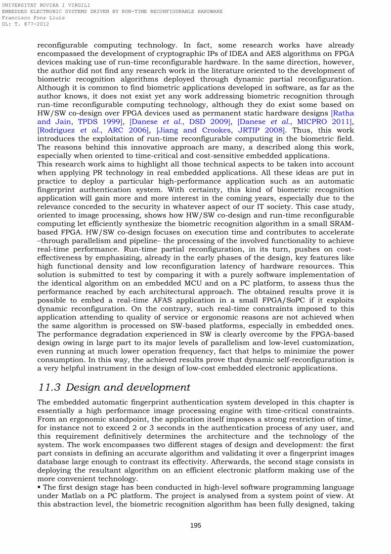
195
reconfigurable computing technology. In fact, some research works have already encompassed the development of cryptographic IPs of IDEA and AES algorithms on FPGA devices making use of run-time reconfigurable hardware. In the same direction, however, the author did not find any research work in the literature oriented to the development of biometric recognition algorithms deployed through dynamic partial reconfiguration. Although it is common to find biometric applications developed in software, as far as the author knows, it does not exist yet any work addressing biometric recognition through run-time reconfigurable computing technology, although they do exist some based on HW/SW co-design over FPGA devices used as permanent static hardware designs [Ratha and Jain, TPDS 1999], [Danese et al., DSD 2009], [Danese et al., MICPRO 2011], [Rodríguez et al., ARC 2006], [Jiang and Crookes, JRTIP 2008]. Thus, this work introduces the exploitation of run-time reconfigurable computing in the biometric field. The reasons behind this innovative approach are many, a described along this work, especially when oriented to time-critical and cost-sensitive embedded applications. This research work aims to highlight all those technical aspects to be taken into account when applying PR technology in real embedded applications. All these ideas are put in practice to deploy a particular high-performance application such as an automatic fingerprint authentication system. With certainty, this kind of biometric recognition application will gain more and more interest in the coming years, especially due to the relevance conceded to the security in whatever aspect of our IT society. This case study, oriented to image processing, shows how HW/SW co-design and run-time reconfigurable computing let efficiently synthesize the biometric recognition algorithm in a small SRAM-based FPGA. HW/SW co-design focuses on execution time and contributes to accelerate –through parallelism and pipeline– the processing of the involved functionality to achieve real-time performance. Run-time partial reconfiguration, in its turn, pushes on cost-effectiveness by emphasizing, already in the early phases of the design, key features like high functional density and low reconfiguration latency of hardware resources. This solution is submitted to test by comparing it with a purely software implementation of the identical algorithm on an embedded MCU and on a PC platform, to assess thus the performance reached by each architectural approach. The obtained results prove it is possible to embed a real-time AFAS application in a small FPGA/SoPC if it exploits dynamic reconfiguration. On the contrary, such real-time constraints imposed to this application attending to quality of service or ergonomic reasons are not achieved when the same algorithm is processed on SW-based platforms, especially in embedded ones. The performance degradation experienced in SW is clearly overcome by the FPGA-based design owing in large part to its major levels of parallelism and low-level customization, even running at much lower operation frequency, fact that helps to minimize the power consumption. In this way, the achieved results prove that dynamic self-reconfiguration is a very helpful instrument in the design of low-cost embedded electronic applications.
11.3 Design and development
The embedded automatic fingerprint authentication system developed in this chapter is essentially a high performance image processing engine with time-critical constraints. From an ergonomic standpoint, the application itself imposes a strong restriction of time, for instance not to exceed 2 or 3 seconds in the authentication process of any user, and this requirement definitively determines the architecture and the technology of the system. The work encompasses two different stages of design and development: the first part consists in defining an accurate algorithm and validating it over a fingerprint images database large enough to contrast its effectivity. Afterwards, the second stage consists in deploying the resultant algorithm on an efficient electronic platform making use of the more convenient technology. The first design stage has been conducted in high-level software programming language under Matlab on a PC platform. The project is analysed from a system point of view. At this abstraction level, the biometric recognition algorithm has been fully designed, taking
UNIVERSITAT ROVIRA I VIRGILI EMBEDDED ELECTRONIC SYSTEMS DRIVEN BY RUN-TIME RECONFIGURABLE HARDWARE Francisco Fons Lluís DL: T. 877-2012
196
as guide or reference certain state-of-the-art biometric computing algorithms found in the literature. Hence, the different processing stages required to ensure a good level of confidency in performing the recognition of the fingerprint samples are defined at this stage clearly focused on algorithmic aspects, and the biometric algorithm is fully validated submitting it to large databases of public fingerprint images. The second stage turns around the efficient implementation on an electronic embedded system able to support the resultant algorithm designed in the previous stage. For this, first of all the software algorithm described in Matlab is rewritten in C programming language under Microsoft Visual Studio v6.0 (Visual C++) environment in order to be ported and adapted to the characteristics of an embedded software platform. This new version of the algorithm is executed first on the PC platform, just to confirm that we obtain the same logical results than when executed in Matlab. In this way it is confirmed the porting from Matlab code to C code is correct. Once the algorithm is described in C code and the different tasks of this batch process are properly identified, it is feasible to make a first profiling of the different stages involved in the recognition algorithm already on a PC platform to identify the more time consuming functions. However, the same algorithm described in C is also ported to several embedded microprocessor platforms in order to make a more accurate and realistic profiling since as final goal this algorithm is intended to be lodged in embedded platforms instead of HPC platforms. This fact implies to optimize the implementation already at this point, for instance considering necessary the usage of integers instead of floating-point data if with this decision it is possible to improve performance without degradating data accuracy. Other design rules adopted here are not to use certain powerful but expensive libraries of signal processing if they involve too much resources when running on an embedded platform, or not to use excessive RAM data to store intermediate data/images if this amount is not be available in the platform where it is finally decided to synthesize the application, etc. The analysis of this software-based solution brings an important feedback concerning costs (execution time, memory requirements, etc) of each task involved in the algorithm, information that is used to decide key architectural aspects like the HW/SW partitioning of tasks and the proper dimensioning of the communication interfaces. Just in this step, through the profiling of the application, it is possible to find out which are the more compute-intensive tasks to be implemented in hardware whereas the less time-critical tasks can be kept in software. With all this information, the SW tasks are described in C programming language and the HW tasks in VHDL hardware description language over logic programmable resources. Concurrently, both hardware co-processors and software functions are co-verified with appropiate SoC development tools. Until now the system is designed statically, i.e. with coprocessors that stay in the system for all the application lifetime. The following step of the design flow consists in the temporal partitioning of the application by updating the HW tasks in the same set of shared resources of the programmable logic device. For this, from all the tasks identified in the bach process, the ones implemented in hardware can share in time their hardware resources if they are not required at the same time, and dynamically while the rest of the system is running. The aim of this stage is to optimize the hardware costs of the system, multiplexing in time the silicon area of the FPGA and being able, thus, to implement the application in a smaller FPGA device. By temporally partitioning the algorithm, the system can locate different logical circuitries into the same device every time, what makes possible to save area. In this way, the MCU downloads the bitstream to the partial or total part of the FPGA in order to change its functional behavior at the same time as the system is evolving without stopping the processing. Finally, once the system is verified and validated, a prototype can be implemented either designing a new PCB or just using a commercial evaluation board equipped with the resources needed, where basically only one chip performs all the digital processing of the biometric algorithm. As a final integration test, the system prototype has been validated on real fingerprint images acquired by the system as well as on other fingerprint images that exist in public
UNIVERSITAT ROVIRA I VIRGILI EMBEDDED ELECTRONIC SYSTEMS DRIVEN BY RUN-TIME RECONFIGURABLE HARDWARE Francisco Fons Lluís DL: T. 877-2012
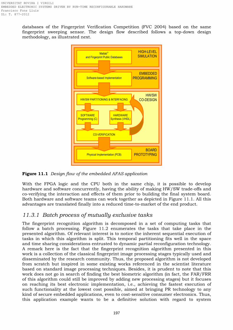
197
databases of the Fingerprint Verification Competition (FVC 2004) based on the same fingerprint sweeping sensor. The design flow described follows a top-down design methodology, as illustrated next. Figure 11.1 Design flow of the embedded AFAS application With the FPGA logic and the CPU both in the same chip, it is possible to develop hardware and software concurrently, having the ability of making HW/SW trade-offs and co-verifying the interaction and effects of them prior to building the final system board. Both hardware and software teams can work together as depicted in Figure 11.1. All this advantages are translated finally into a reduced time-to-market of the end product.
11.3.1 Batch process of mutually exclusive tasks
The fingerprint recognition algorithm is decomposed in a set of computing tasks that follow a batch processing. Figure 11.2 enumerates the tasks that take place in the presented algorithm. Of relevant interest is to notice the inherent sequential execution of tasks in which this algorithm is split. This temporal partitioning fits well in the space and time sharing considerations entrusted to dynamic partial reconfiguration technology. A remark here is the fact that the fingerprint recognition algorithm presented in this work is a collection of the classical fingerprint image processing stages typically used and disseminated by the research community. Thus, the proposed algorithm is not developed from scratch but inspired in some existing works referenced in the scientist literature based on standard image processing techniques. Besides, it is prudent to note that this work does not go in search of finding the best biometric algorithm (in fact, the FAR/FRR of this algorithm could still be improved by adding new processing stages) but it focuses on reaching its best electronic implementation, i.e., achieving the fastest execution of such functionality at the lowest cost possible, aimed at bringing PR technology to any kind of secure embedded applications, even to cost-sensitive consumer electronics. Thus, this application example wants to be a definitive solution with regard to system
HW/SW CO-DESIGN
HIGH-LEVEL SIMULATION
BOARD PROTOTYPING
EMBEDDED PROGRAMMING
Matlab
and Fingerprint Public Databases
SOFTWARE Programming (C)
HARDWARE Synthesis (VHDL)
Software-based Implementation
HW/SW PARTITIONING & INTERFACING
CO-VERIFICATION
Physical Implementation (PCB)
UNIVERSITAT ROVIRA I VIRGILI EMBEDDED ELECTRONIC SYSTEMS DRIVEN BY RUN-TIME RECONFIGURABLE HARDWARE Francisco Fons Lluís DL: T. 877-2012
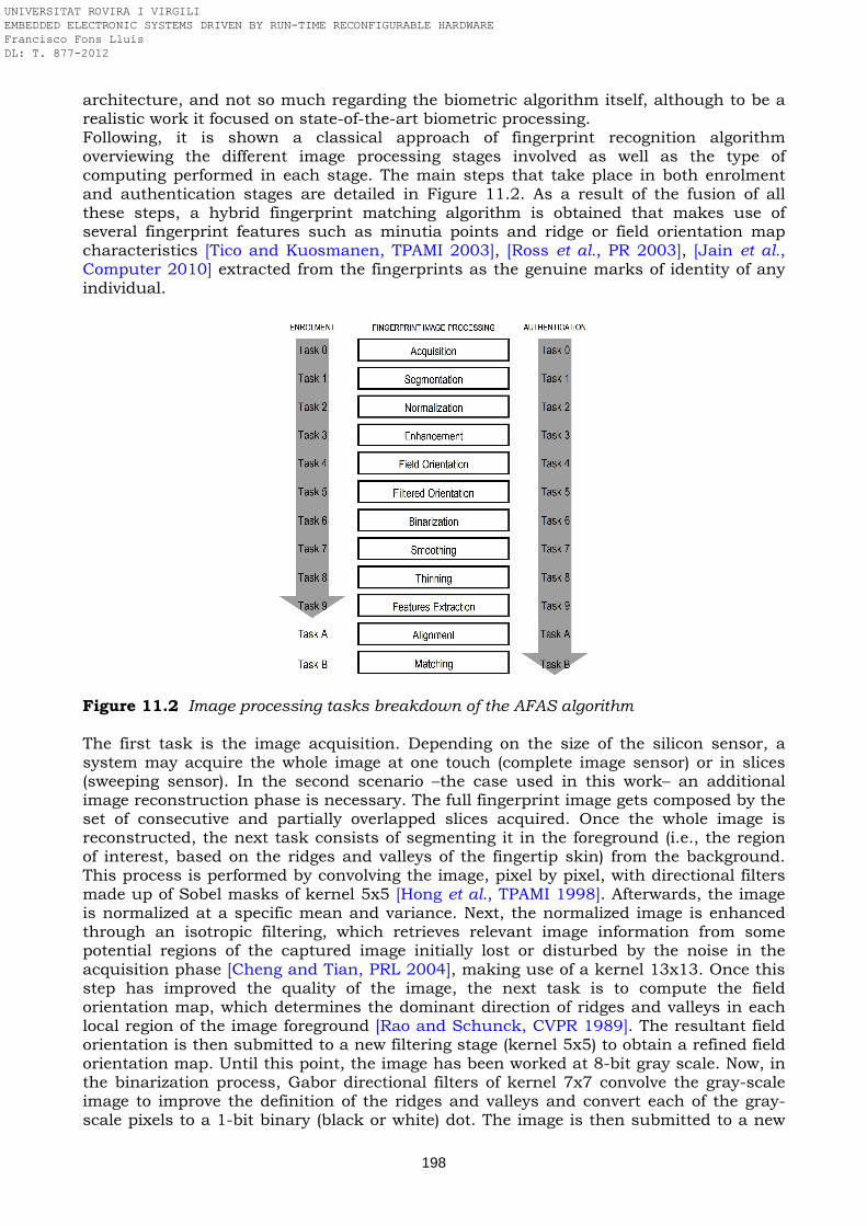
198
architecture, and not so much regarding the biometric algorithm itself, although to be a realistic work it focused on state-of-the-art biometric processing. Following, it is shown a classical approach of fingerprint recognition algorithm overviewing the different image processing stages involved as well as the type of computing performed in each stage. The main steps that take place in both enrolment and authentication stages are detailed in Figure 11.2. As a result of the fusion of all these steps, a hybrid fingerprint matching algorithm is obtained that makes use of several fingerprint features such as minutia points and ridge or field orientation map characteristics [Tico and Kuosmanen, TPAMI 2003], [Ross et al., PR 2003], [Jain et al., Computer 2010] extracted from the fingerprints as the genuine marks of identity of any individual.
Figure 11.2 Image processing tasks breakdown of the AFAS algorithm The first task is the image acquisition. Depending on the size of the silicon sensor, a system may acquire the whole image at one touch (complete image sensor) or in slices (sweeping sensor). In the second scenario –the case used in this work– an additional image reconstruction phase is necessary. The full fingerprint image gets composed by the set of consecutive and partially overlapped slices acquired. Once the whole image is reconstructed, the next task consists of segmenting it in the foreground (i.e., the region of interest, based on the ridges and valleys of the fingertip skin) from the background. This process is performed by convolving the image, pixel by pixel, with directional filters made up of Sobel masks of kernel 5x5 [Hong et al., TPAMI 1998]. Afterwards, the image is normalized at a specific mean and variance. Next, the normalized image is enhanced through an isotropic filtering, which retrieves relevant image information from some potential regions of the captured image initially lost or disturbed by the noise in the acquisition phase [Cheng and Tian, PRL 2004], making use of a kernel 13x13. Once this step has improved the quality of the image, the next task is to compute the field orientation map, which determines the dominant direction of ridges and valleys in each local region of the image foreground [Rao and Schunck, CVPR 1989]. The resultant field orientation is then submitted to a new filtering stage (kernel 5x5) to obtain a refined field orientation map. Until this point, the image has been worked at 8-bit gray scale. Now, in the binarization process, Gabor directional filters of kernel 7x7 convolve the gray-scale image to improve the definition of the ridges and valleys and convert each of the gray-scale pixels to a 1-bit binary (black or white) dot. The image is then submitted to a new
UNIVERSITAT ROVIRA I VIRGILI EMBEDDED ELECTRONIC SYSTEMS DRIVEN BY RUN-TIME RECONFIGURABLE HARDWARE Francisco Fons Lluís DL: T. 877-2012
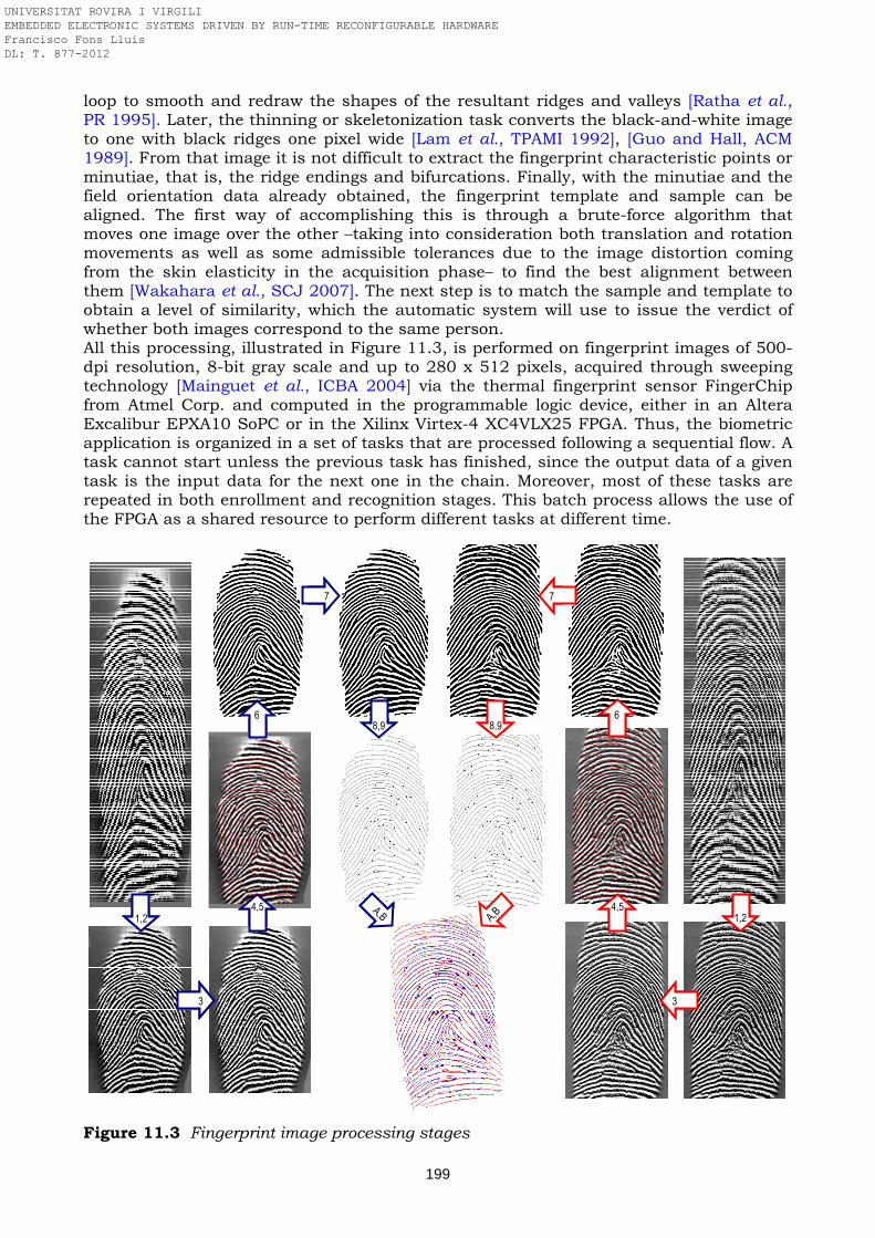
199
loop to smooth and redraw the shapes of the resultant ridges and valleys [Ratha et al., PR 1995]. Later, the thinning or skeletonization task converts the black-and-white image to one with black ridges one pixel wide [Lam et al., TPAMI 1992], [Guo and Hall, ACM 1989]. From that image it is not difficult to extract the fingerprint characteristic points or minutiae, that is, the ridge endings and bifurcations. Finally, with the minutiae and the field orientation data already obtained, the fingerprint template and sample can be aligned. The first way of accomplishing this is through a brute-force algorithm that moves one image over the other –taking into consideration both translation and rotation movements as well as some admissible tolerances due to the image distortion coming from the skin elasticity in the acquisition phase– to find the best alignment between them [Wakahara et al., SCJ 2007]. The next step is to match the sample and template to obtain a level of similarity, which the automatic system will use to issue the verdict of whether both images correspond to the same person. All this processing, illustrated in Figure 11.3, is performed on fingerprint images of 500-dpi resolution, 8-bit gray scale and up to 280 x 512 pixels, acquired through sweeping technology [Mainguet et al., ICBA 2004] via the thermal fingerprint sensor FingerChip from Atmel Corp. and computed in the programmable logic device, either in an Altera Excalibur EPXA10 SoPC or in the Xilinx Virtex-4 XC4VLX25 FPGA. Thus, the biometric application is organized in a set of tasks that are processed following a sequential flow. A task cannot start unless the previous task has finished, since the output data of a given task is the input data for the next one in the chain. Moreover, most of these tasks are repeated in both enrollment and recognition stages. This batch process allows the use of the FPGA as a shared resource to perform different tasks at different time.
A,B A,B1,2
3 3
1,24,5 4,5
6 6
7 7
8,9 8,9
A,B A,B1,2
3 3
1,24,5 4,5
6 6
7 7
8,9 8,9
Figure 11.3 Fingerprint image processing stages
UNIVERSITAT ROVIRA I VIRGILI EMBEDDED ELECTRONIC SYSTEMS DRIVEN BY RUN-TIME RECONFIGURABLE HARDWARE Francisco Fons Lluís DL: T. 877-2012
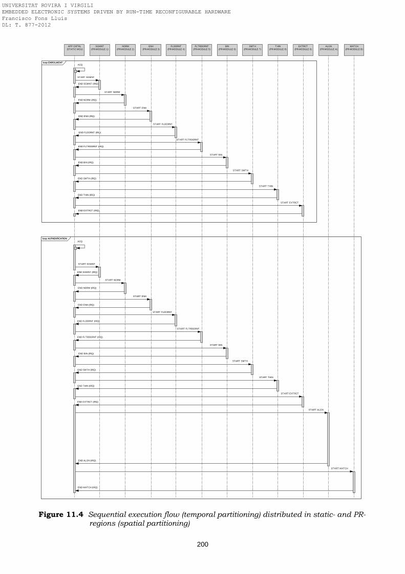
200
APP CNTRL(STATIC MCU)
MATCH(PR-MODULE B)
ALGN(PR-MODULE A)
EXTRCT(PR-MODULE 9)
THIN (PR-MODULE 8)
SMTH(PR-MODULE 7)
BIN (PR-MODULE 6)
FLTRDORNT(PR-MODULE 5)
FLDORNT(PR-MODULE 4)
loop ENROLMENT
ENH (PR-MODULE 3)
loop AUTHENTICATION
NORM(PR-MODULE 2)
SGMNT(PR-MODULE 1)
ACQ
START SGMNT
END SGMNT (IRQ)
START NORM
END NORM (IRQ)
START ENH
END ENH (IRQ)
START FLDORNT
END FLDORNT (IRQ)
START FLTRDORNT
END FLTRDORNT (IRQ)
START BIN
END BIN (IRQ)
START SMTH
END SMTH (IRQ)
START THIN
END THIN (IRQ)
START EXTRCT
END EXTRCT (IRQ)
ACQ
START SGMNT
END SGMNT (IRQ)
START NORM
END NORM (IRQ)
START ENH
END ENH (IRQ)
START FLDORNT
END FLDORNT (IRQ)
START FLTRDORNT
END FLTRDORNT (IRQ)
START BIN
END BIN (IRQ)
START SMTH
END SMTH (IRQ)
START THIN
END THIN (IRQ)
START EXTRCT
END EXTRCT (IRQ)
START ALGN
END ALGN (IRQ)
START MATCH
END MATCH (IRQ)
Figure 11.4 Sequential execution flow (temporal partitioning) distributed in static- and PR-regions (spatial partitioning)
UNIVERSITAT ROVIRA I VIRGILI EMBEDDED ELECTRONIC SYSTEMS DRIVEN BY RUN-TIME RECONFIGURABLE HARDWARE Francisco Fons Lluís DL: T. 877-2012
201
11.3.2 Spatial and temporal partitioning of tasks
Figure 11.2 identifies the different processing stages of the AFAS application. Each of these sequential stages, in its turn, can be implemented in a set of hardware and software tasks processed in serial or parallel. The software tasks are left to the host CPU of the system. The hardware tasks are performed in several custom master or slave coprocessors in connection with the CPU. Figure 11.4 shows the partitioning of tasks identifying up to 12 sequential stages. From these stages, the first one (acquisition) and the last two (alignment and matching) combine tasks in software and hardware at the same time. The other 10 out of 12 stages are described in VHDL to be totally synthesized in custom hardware. All these coprocessors are designed following a pipelined architecture and the implementation exhibits a great deal of parallelism in order to guarantee a real-time authentication response. Furthermore, since all these stages are mutually exclusive as depicted in the sequence diagram of Figure 11.4, they can be multiplexed in time in an area of the programmable logic device, becoming this area a shared resource. This strategy enhances the functional density of the resources in use, in exchange for minimizing the number of resources required. However, as overhead, the reconfiguration latency of these shared resources is added to the original processing time of each computational stage. The spatial partitioning of the application in static hardware and reconfigurable hardware has been experimented in two different platforms. First, in a SoPC device composed of a hard-core host processor and an FPGA that admits to perform a full reconfiguration conducted by the host CPU. The second option is based on a run-time partially reconfigurable FPGA partitioned in a static region and a PR region. In this case, the static region lodges a soft-core processor and the PR region is addressed to allocate the different hardware coprocessors. In this way the PR region of the FPGA device can be reconfigured on the fly while this reconfiguration process is managed from the static region. These two different implementation approaches carried out in this work are detailed in the next section.
11.4 Experimental results
Two scenarios have been evaluated, both exploring run-time reconfiguration. In the first one, the system is embedded in an Altera Excalibur SoPC device composed of a hard-core processor (ARM9) and an FPGA. In this case, the FPGA –an Altera APEX20KE– is totally reconfigured in several stages to swap there in and out new coprocessors each time. In the second approach, the same concept is applied to an FPGA device provided with dynamic partial reconfiguration capability, to be exact the Xilinx Virtex-4 LX device. In this case, the system is composed of a soft-core processor (MicroBlaze) instantiated in a static region of the FPGA and a partially reconfigurable region is used as a shared resource where different coprocessors can be placed and removed along the execution of the application. In this second approach, the shared resource is not all the FPGA but only a partition. For this, the FPGA is built with PR glitchless technology and admits run-time partial reconfiguration. The technical features of the reconfiguration engine of these two platforms –Excalibur SoPC and Virtex-4 FPGA– have been described in detail in chapter 5. From the point of view of reconfiguration granularity for the application, in the first approach several hardware coprocessors coexist at the same time in one context of the FPGA and they are swapped by other set of coprocessors when the FPGA is fully reconfigured. In the second approach this reconfiguration granularity is reduced to only one coprocessor that fits in a more reduced area consisting of a PR region of the FPGA. The reason to implement compute intensive tasks in hardware instead of software is due basically to reduce the execution time of the application, to perform it at real-time by exploiting parallelism. The two run-time reconfiguration alternatives –based on full or partial reconfiguration of an FPGA device– pursue to minimize the programmable logic
UNIVERSITAT ROVIRA I VIRGILI EMBEDDED ELECTRONIC SYSTEMS DRIVEN BY RUN-TIME RECONFIGURABLE HARDWARE Francisco Fons Lluís DL: T. 877-2012
202
resources required to implement the AFAS solution given that a full AFAS approach implemented with all the hardware accelerators synthesized in a static and permanent way on silicon would penalize too much in cost in comparison to a software-based solution on a MCU device. Furthermore, in the reconfigurable solution proposed, the time spent on the (full or partial) FPGA reconfiguration is part of the application execution time and shall be minimized. The implementation benchmark of the AFAS either as a pure software approach on a PC platform under a dual-core processor (Intel Core 2 Duo T5600 at 1.83 GHz) or as a reconfigurable SoPC/FPGA co-design (identical algorithm partitioned in HW/SW tasks operating in the range of tens of MHz on the the Altera Excalibur EPXA10 SoPC or the Xilinx Virtex-4 XC4VLX25 FPGA) highlights a speed-up of one order of magnitude in favor of the SoPC/FPGA alternative. This acceleration rate grows up to two orders of magnitude when such run-time reconfigurable alternative is compared with a SW solution based on an embedded MCU platform running at hundreds of MHz instead of a PC system running at GHz. These results let point out biometric recognition as a sensible killer application for run-time reconfigurable computing, mainly in terms of efficiently balancing computational power, functional flexibility and cost. Such features, reached through dynamic reconfiguration, are easily portable today to a broad range of embedded applications with identical system architecture.
11.4.1 Approach I: Full FPGA reconfiguration on Excalibur SoPC
The combination of hardware acceleration and flexibility makes reconfigurable SRAM-based FPGAs key devices for implementing efficient computing systems. These, when interfaced to a microcontroller unit, let move the most demanding processing tasks into dedicated HW coprocessors. Thus, the traditional way of implementing algorithms only in SW is nowadays a more and more obsolete practice, especially in the image processing field where the current generation of FPGAs, with reconfigurable digital signal processing resources as well as embedded processors, is gradually attracting the interest of this market with powerful SoC platforms. In this direction, this work looks for exploiting the benefits of developing an embedded AFAS prototype able to achieve good levels of security at low cost under an efficient HW-SW architecture. The development platform is constituted by the Altera Excalibur EPXA10 SoPC, as illustrated in Figure 11.5. This device integrates an ARM922T core processor, standard peripherals, programmable logic resources collected in a 1Mgates APEX20KE FPGA and both on-chip single-port and dual-port SRAM memory blocks shared by the ARM processor and the FPGA. All these components are linked through two internal AMBA AHB interfaces. In addition to the EPXA10 device, the development setup is equipped with an Atmel FingerChip FCD4B14 fingerprint sensor, which is directly connected to the FPGA by means of a dedicated HW controller in order to acquire the fingerprint images of the user. Next, external SDRAM memory, interfaced to a SDRAM controller present in the SoPC, stores the fingerprint images and lets access to them from both MCU (considering the embedded stripe composed of ARM core, memory and peripherals) and FPGA sides. Another external memory available in our AFAS prototype is Flash. This non-volatile memory stores several bitstreams corresponding to the different HW contexts that are sequentially downloaded into the FPGA while the biometric algorithm is in progress. Just for this, the EPXA10 SoPC integrates a configuration controller from where the MCU can handle the reconfiguration of the FPGA resources at any time during system operation. Thus, inside the FPGA, it is instantiated a dedicated arithmetic coprocessor to perform the specific computation needed each time. This evolvable coprocessor is connected to the internal DP-SRAM accessible by the ARM processor and the FPGA through an Altera AVALON controller. This dual-port memory is used to store partial data computed in a task that could be accessed or shared by both processors in some other task. Furthermore, it has been implemented an AHB master controller in the FPGA to access to the AHB-based devices, especially the SDRAM controller which connects with the
UNIVERSITAT ROVIRA I VIRGILI EMBEDDED ELECTRONIC SYSTEMS DRIVEN BY RUN-TIME RECONFIGURABLE HARDWARE Francisco Fons Lluís DL: T. 877-2012
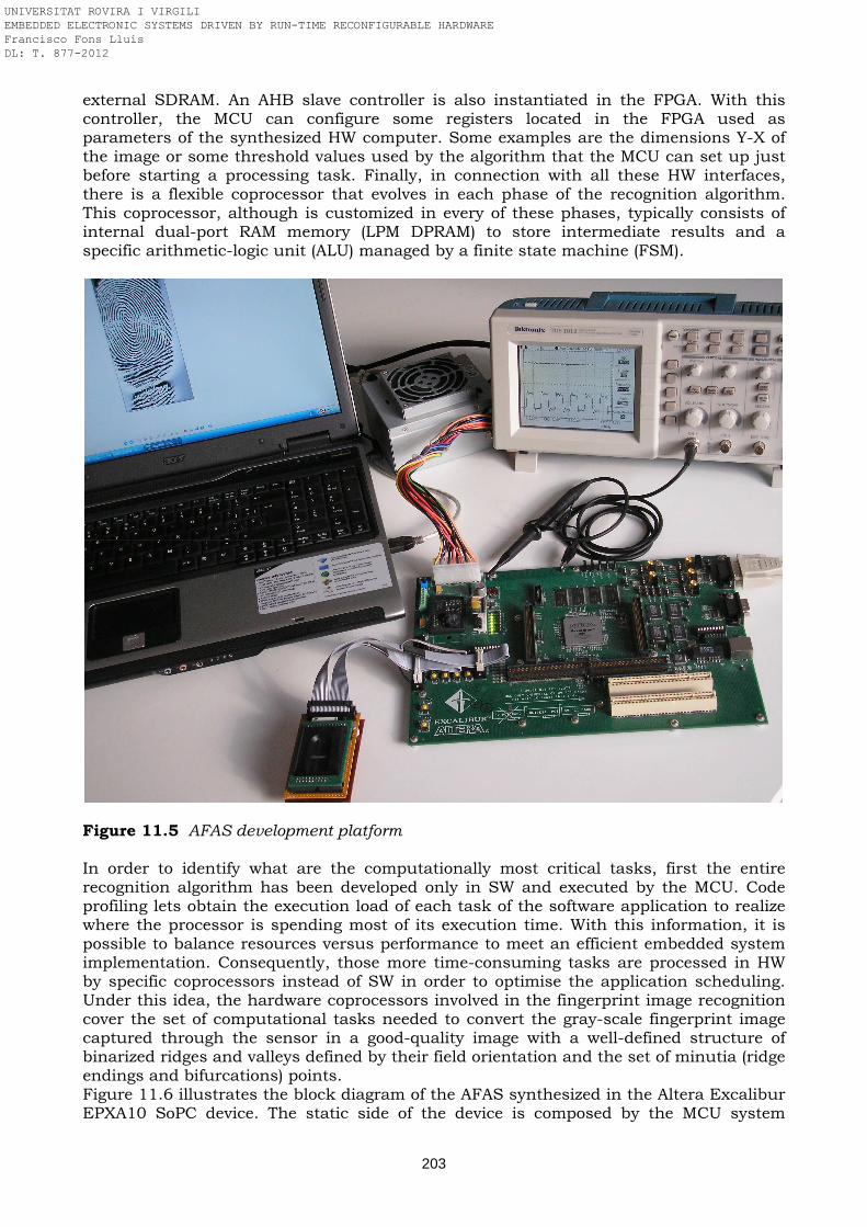
203
external SDRAM. An AHB slave controller is also instantiated in the FPGA. With this controller, the MCU can configure some registers located in the FPGA used as parameters of the synthesized HW computer. Some examples are the dimensions Y-X of the image or some threshold values used by the algorithm that the MCU can set up just before starting a processing task. Finally, in connection with all these HW interfaces, there is a flexible coprocessor that evolves in each phase of the recognition algorithm. This coprocessor, although is customized in every of these phases, typically consists of internal dual-port RAM memory (LPM DPRAM) to store intermediate results and a specific arithmetic-logic unit (ALU) managed by a finite state machine (FSM).
Figure 11.5 AFAS development platform In order to identify what are the computationally most critical tasks, first the entire recognition algorithm has been developed only in SW and executed by the MCU. Code profiling lets obtain the execution load of each task of the software application to realize where the processor is spending most of its execution time. With this information, it is possible to balance resources versus performance to meet an efficient embedded system implementation. Consequently, those more time-consuming tasks are processed in HW by specific coprocessors instead of SW in order to optimise the application scheduling. Under this idea, the hardware coprocessors involved in the fingerprint image recognition cover the set of computational tasks needed to convert the gray-scale fingerprint image captured through the sensor in a good-quality image with a well-defined structure of binarized ridges and valleys defined by their field orientation and the set of minutia (ridge endings and bifurcations) points. Figure 11.6 illustrates the block diagram of the AFAS synthesized in the Altera Excalibur EPXA10 SoPC device. The static side of the device is composed by the MCU system
UNIVERSITAT ROVIRA I VIRGILI EMBEDDED ELECTRONIC SYSTEMS DRIVEN BY RUN-TIME RECONFIGURABLE HARDWARE Francisco Fons Lluís DL: T. 877-2012
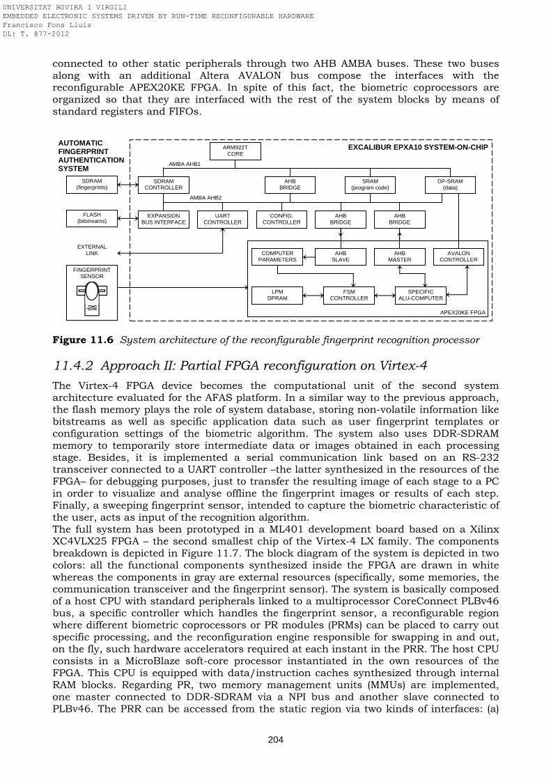
204
connected to other static peripherals through two AHB AMBA buses. These two buses along with an additional Altera AVALON bus compose the interfaces with the reconfigurable APEX20KE FPGA. In spite of this fact, the biometric coprocessors are organized so that they are interfaced with the rest of the system blocks by means of standard registers and FIFOs.
Figure 11.6 System architecture of the reconfigurable fingerprint recognition processor
11.4.2 Approach II: Partial FPGA reconfiguration on Virtex-4
The Virtex-4 FPGA device becomes the computational unit of the second system architecture evaluated for the AFAS platform. In a similar way to the previous approach, the flash memory plays the role of system database, storing non-volatile information like bitstreams as well as specific application data such as user fingerprint templates or configuration settings of the biometric algorithm. The system also uses DDR-SDRAM memory to temporarily store intermediate data or images obtained in each processing stage. Besides, it is implemented a serial communication link based on an RS-232 transceiver connected to a UART controller –the latter synthesized in the resources of the FPGA– for debugging purposes, just to transfer the resulting image of each stage to a PC in order to visualize and analyse offline the fingerprint images or results of each step. Finally, a sweeping fingerprint sensor, intended to capture the biometric characteristic of the user, acts as input of the recognition algorithm. The full system has been prototyped in a ML401 development board based on a Xilinx XC4VLX25 FPGA – the second smallest chip of the Virtex-4 LX family. The components breakdown is depicted in Figure 11.7. The block diagram of the system is depicted in two colors: all the functional components synthesized inside the FPGA are drawn in white whereas the components in gray are external resources (specifically, some memories, the communication transceiver and the fingerprint sensor). The system is basically composed of a host CPU with standard peripherals linked to a multiprocessor CoreConnect PLBv46 bus, a specific controller which handles the fingerprint sensor, a reconfigurable region where different biometric coprocessors or PR modules (PRMs) can be placed to carry out specific processing, and the reconfiguration engine responsible for swapping in and out, on the fly, such hardware accelerators required at each instant in the PRR. The host CPU consists in a MicroBlaze soft-core processor instantiated in the own resources of the FPGA. This CPU is equipped with data/instruction caches synthesized through internal RAM blocks. Regarding PR, two memory management units (MMUs) are implemented, one master connected to DDR-SDRAM via a NPI bus and another slave connected to PLBv46. The PRR can be accessed from the static region via two kinds of interfaces: (a)
FINGERPRINT SENSOR
AUTOMATIC FINGERPRINT AUTHENTICATION SYSTEM
APEX20KE FPGA
EXCALIBUR EPXA10 SYSTEM-ON-CHIP
AMBA AHB1
AMBA AHB2
SDRAM CONTROLLER
ARM922T CORE
DP-SRAM (data)
SRAM (program code)
AHB BRIDGE
EXPANSION BUS INTERFACE
CONFIG. CONTROLLER
AHB BRIDGE
AHB BRIDGE
AHB SLAVE
AHB MASTER
LPM DPRAM
SPECIFIC ALU-COMPUTER
AVALON CONTROLLER
UART CONTROLLER
COMPUTER PARAMETERS
FSM CONTROLLER
SDRAM (fingerprints)
FLASH (bitstreams)
EXTERNAL
LINK
UNIVERSITAT ROVIRA I VIRGILI EMBEDDED ELECTRONIC SYSTEMS DRIVEN BY RUN-TIME RECONFIGURABLE HARDWARE Francisco Fons Lluís DL: T. 877-2012
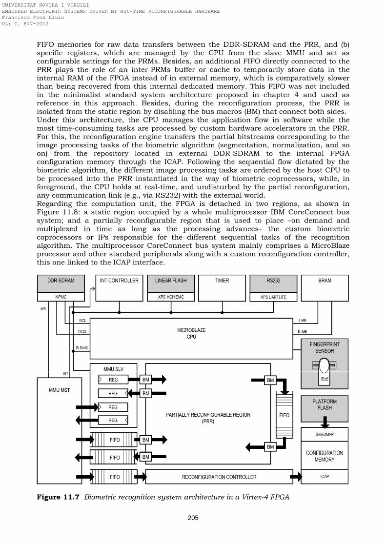
205
FIFO memories for raw data transfers between the DDR-SDRAM and the PRR, and (b) specific registers, which are managed by the CPU from the slave MMU and act as configurable settings for the PRMs. Besides, an additional FIFO directly connected to the PRR plays the role of an inter-PRMs buffer or cache to temporarily store data in the internal RAM of the FPGA instead of in external memory, which is comparatively slower than being recovered from this internal dedicated memory. This FIFO was not included in the minimalist standard system architecture proposed in chapter 4 and used as reference in this approach. Besides, during the reconfiguration process, the PRR is isolated from the static region by disabling the bus macros (BM) that connect both sides. Under this architecture, the CPU manages the application flow in software while the most time-consuming tasks are processed by custom hardware accelerators in the PRR. For this, the reconfiguration engine transfers the partial bitstreams corresponding to the image processing tasks of the biometric algorithm (segmentation, normalization, and so on) from the repository located in external DDR-SDRAM to the internal FPGA configuration memory through the ICAP. Following the sequential flow dictated by the biometric algorithm, the different image processing tasks are ordered by the host CPU to be processed into the PRR instantiated in the way of biometric coprocessors, while, in foreground, the CPU holds at real-time, and undisturbed by the partial reconfiguration, any communication link (e.g., via RS232) with the external world. Regarding the computation unit, the FPGA is detached in two regions, as shown in Figure 11.8: a static region occupied by a whole multiprocessor IBM CoreConnect bus system; and a partially reconfigurable region that is used to place –on demand and multiplexed in time as long as the processing advances– the custom biometric coprocessors or IPs responsible for the different sequential tasks of the recognition algorithm. The multiprocessor CoreConnect bus system mainly comprises a MicroBlaze processor and other standard peripherals along with a custom reconfiguration controller, this one linked to the ICAP interface.
Figure 11.7 Biometric recognition system architecture in a Virtex-4 FPGA
UNIVERSITAT ROVIRA I VIRGILI EMBEDDED ELECTRONIC SYSTEMS DRIVEN BY RUN-TIME RECONFIGURABLE HARDWARE Francisco Fons Lluís DL: T. 877-2012
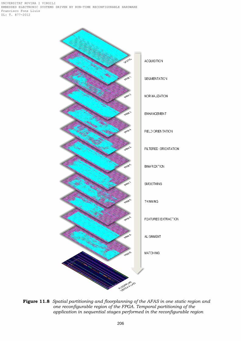
206
Figure 11.8 Spatial partitioning and floorplanning of the AFAS in one static region and one reconfigurable region of the FPGA. Temporal partitioning of the application in sequential stages performed in the reconfigurable region
UNIVERSITAT ROVIRA I VIRGILI EMBEDDED ELECTRONIC SYSTEMS DRIVEN BY RUN-TIME RECONFIGURABLE HARDWARE Francisco Fons Lluís DL: T. 877-2012
207
All the processing tasks are enumerated from 0 (static) to B in Figure 11.2, according to sequential execution order. Custom hardware coprocessors implement all the tasks in the PRR, with the exception of the fingerprint acquisition process which is performed in software by MicroBlaze. The reason behind this specific hardware/software partitioning is that the sweeping sensor needs an integration time of 5 milliseconds to acquire consecutive slices. That is enough time for it to perform the image reconstruction on the fly directly in software under MicroBlaze control. Therefore, it is not necessary to implement this image reconstruction with a custom hardware coprocessor. The image acquisition consists of capturing 100 slices at a rate of 5 ms per slice, with each slice consisting of 280 x 8 pixels. Software handles the reconstruction in real-time by detecting the overlapping of rows of pixels between each two consecutives image slices. The rest of the tasks, however, are implemented as custom hardware coprocessors in the PRR of the FPGA simply because of real-time constraints. Moreover, regarding tasks partitioning, each task involves the transfer of many data –typically the full fingerprint image– from external memory to the PRR where it is processed and back to external memory. Each of these tasks has been scheduled in a different coprocessor. Once the processing of each particular task is finished, the reconfiguration controller –located on the static region of the device and instructed by the MicroBlaze processor– replaces the coprocessor currently instantiated in the PRR by the one corresponding to the next stage of the biometric algorithm. The reconfiguration controller does this job by simply downloading the new partial bitstream into the PRR and transferring this data directly from DDR-SDRAM to the internal FPGA configuration memory via the ICAP interface. It is important to note that it is used a standard interface based on FIFO memories and flip-flop registers between the static and the reconfigurable regions. This allows to develop standard biometric coprocessors or IPs placed in the PRR which are independent of the multiprocessor bus the system uses, be it AMBA, CoreConnect, Wishbone or some other, as depicted in Figure 11.7. This point is fundamental in order to guarantee standardization and portability of the biometric algorithm to different platforms.
11.4.3 Performance evaluation
The AFAS application can be classified as a high-performance image processing transaction since it exhibits a great deal of parallelism and demands a real-time authentication response, what from an ergonomic standpoint means not to exceed some few seconds. Furthermore, despite the implementation trade-off between processing time and consumed resources, a low cost solution is mandatory if we pursue to port this technical proposal also to high volume consumer applications. Submitted to all these constraints, the system architecture presented in our approach is centered in a computation unit driven by hardware/software co-design and run-time reconfiguration technologies applied to programmable logic devices. In general, the verification efficiency of two different biometric algorithms can be compared by evaluating their accuracy in identifying (or rejecting) a same set of genuine (or fraudulent) users trying to access to the system. The equal error rate (EER), false acceptance rate (FAR) or false rejection rate (FRR) are addressed to this aim. However, to assess the implementation efficiency of an algorithm against different technological approaches (e.g., software-oriented solutions on a GPU or MCU, or HW/SW co-design on an FPGA), the metrics in use are mainly the execution time spent (i.e., ergonomics) and the physical resources involved (i.e., cost). Just for this reason, we have submitted our algorithm to several implementation approaches under different platforms: a SW-based implementation on a PC first and on several embedded MCUs later, and a HW/SW co-design of the same algorithm on a SoPC and on an FPGA in the end making use of PR. As introduced in section 11.3, the design flow entails several development loops. Initially, we fully developed the algorithm in software in Matlab on a PC platform. Afterward, we ported this software code to embedded software in the C programming language and executed it first in the same PC, just to confirm that we would obtain the same results,
UNIVERSITAT ROVIRA I VIRGILI EMBEDDED ELECTRONIC SYSTEMS DRIVEN BY RUN-TIME RECONFIGURABLE HARDWARE Francisco Fons Lluís DL: T. 877-2012
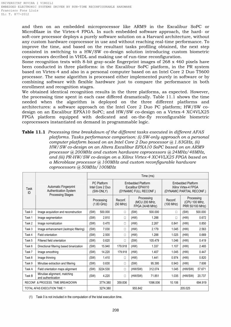
208
and then on an embedded microprocessor like ARM9 in the Excalibur SoPC or MicroBlaze in the Virtex-4 FPGA. In such embedded software approach, the hard- or soft-core processor deploys a purely software solution on a Harvard architecture, without any custom hardware coprocessor in use and without reaching real-time performance. To improve the time, and based on the resultant tasks profiling obtained, the next step consisted in switching to a HW/SW co-design solution introducing custom biometric coprocessors decribed in VHDL and making use of run-time reconfiguration. Some recognition tests with 8-bit gray-scale fingerprint images of 268 x 460 pixels have been conducted in three platforms: in the Excalibur SoPC platform, in the PR system based on Virtex-4 and also in a personal computer based on an Intel Core 2 Duo T5600 processor. The same algorithm is processed either implemented purely in software or by combining software with flexible hardware just to compare the performance in both enrollment and recognition stages. We obtained identical recognition results in the three platforms, as expected. However, the processing time spent in each case differed dramatically. Table 11.1 shows the time needed when the algorithm is deployed on the three different platforms and architectures: a software approach on the Intel Core 2 Duo PC platform; HW/SW co-design on an Excalibur EPXA10 SoPC; and HW/SW co-design on a Virtex-4 XC4VLX25 FPGA platform equipped with dedicated and on-the-fly reconfigurable biometric coprocessors instantiated on demand in programmable logic. Table 11.1 Processing time breakdown of the different tasks executed in different AFAS
platforms. Tasks performance comparison: (i) SW-only approach on a personal computer platform based on an Intel Core 2 Duo processor @ 1.83GHz, (ii) HW/SW co-design on an Altera Excalibur EPXA10 SoPC based on an ARM9 processor @ 200MHz and custom hardware coprocessors @ 24MHz/48MHz, and (iii) PR-HW/SW co-design on a Xilinx Virtex-4 XC4VLX25 FPGA based on a Microblaze processor @ 100MHz and custom reconfigurable hardware coprocessors @ 50MHz/100MHz
Time (ms)
PC Platform Intel Core 2 Duo
(SW-ONLY)
Embedded Platform Excalibur EPAX10
(DYNAMIC FULL RECONF.)
Embedded Platform Xilinx Virtex-4 FPGA
(DYNAMIC PARTIAL RECONF.)
Task
ID
Automatic Fingerprint Authentication System
Processing Stages
Processing (1.83 GHz)
Reconf. (50 MHz)
Processing (MCU 200 MHz,
FPGA 24/48 MHz)
Reconf. (100 MHz)
Processing (CPU 100 MHz,
PRR 50/100 MHz)
Task 0 Image acquisition and reconstruction (SW) 500.000 (SW) 500.000 (SW) 500.000
Task 1 Image segmentation (SW) 2.810 (HW) 1.288 (HW) 0.672
Task 2 Image normalization (SW) 0.470 (HW) 2.267 0.841 (HW) 0.850
Task 3 Image enhancement (isotropic filtering) (SW) 7.030 (HW) 2.179 1.045 (HW) 2.563
Task 4 Field orientation (SW) 2.500 (HW) 1.288 1.025 (HW) 0.669
Task 5 Filtered field orientation (SW) 0.620 (SW) 105.479 1.046 (HW) 0.419
Task 6 Directional filtering based binarization (SW) 15.940 179.918 (HW) 1.337 1.107 (HW) 2.465
Task 7 Image smoothing (SW) 14.220 179.918 (HW) 1.407 1.045 (HW) 0.447
Task 8 Image thinning (SW) 1.410 (HW) 1.441 0.974 (HW) 0.820
Task 9 Minutiae extraction and filtering (SW) 0.630 (SW) 95.395 0.943 (HW) 7.606
Task A Field orientation maps alignment (SW) 3224.530 (HW/SW) 312.074 1.045 (HW/SW) 57.671
Task B Minutiae alignment, matching and authentication
(SW) 4.220 (HW/SW) 71.851 1.035 (HW/SW) 20.737
RECONF. & PROCESS. TIME BREAKDOWN 3774.380 359.836 1096.006 10.106 694.919
TOTAL AFAS EXECUTION TIME (1) 3274.380 955.842 205.025
(1) Task 0 is not included in the computation of the total execution time.
UNIVERSITAT ROVIRA I VIRGILI EMBEDDED ELECTRONIC SYSTEMS DRIVEN BY RUN-TIME RECONFIGURABLE HARDWARE Francisco Fons Lluís DL: T. 877-2012
209
The reconfiguration interface in the Excalibur SoPC is composed of a 1-bit data bus operated at 50 MHz, giving rise to a reconfiguration bandwidth of 50 Mbps. In the Virtex-4 FPGA, the physical features of such interface are 32-bit and 100 MHz, what results in 3.2 Gbps. As deduced from Table 11.1, even though HW/SW approaches add a penalty in time due to the reconfiguration latency (2 full FPGA reconfigurations in the Excalibur approach and up to 10 partial reconfigurations of the PRR in the Virtex-4 approach), this overhead is overcome by the hardware parallelism reached with custom hardware coprocessors. In comparison to the sequential execution of code under a purely software implementation approach in a Harvard-based CPU architecture, an important acceleration rate is achieved with custom coprocessors. As a result, the reconfiguration time is negligible in comparison to the total processing time of the biometric recognition application. Without considering the acquisition task, which is fixed at 500 ms due to the physical sweeping-sensor restrictions (100 slices captured with an integration time of 5 ms and image reconstructed from them on the fly), the reconfigurable system architectures on Excalibur and Virtex-4 let reduce the application execution time due to the rest of the processing tasks to 956 ms and 205 ms respectively. That compares with the latency of 3,274 ms in the pure-software approach on the PC, which means a speedup of 3.4x and 16x in favor of the run-time reconfiguration solution. Thus, Table 11.1 makes it evident that real-time authentication is feasible with HW/SW co-design that exploits parallelism and pipeline techniques, along with run-time reconfigurable hardware technology, thanks to its low reconfiguration latency. But it is not only addressed time in this solution. By means of dynamic reconfiguration, it is intended to reduce cost to the minimum, minimizing the number of resources involved in the design that let achieve the real-time requirements demanded to the application. It has been also carefully considered cost-effectiveness by means of the time-sharing of computational resources. In the first HW/SW co-design prototype based on Excalibur, several coprocessors are synthesized at the same time in the programmable logic to minimize the number of full reconfigurations of the FPGA. In the second prototype on Virtex-4, the number of coprocessors placed at one time is reduced to one and the number of reconfigurations is then increased. This second approach is however the one that reaches a better performance-cost trade-off. The XC4VLX25 FPGA device contains 21,504 slice flip-flops, 21,504 four-input LUTs, 72 18-kbit RAMB16 blocks and 48 DSP48 blocks. Regarding the partitioning of resources in both static and reconfigurable regions, the reconfigurable region takes 11,264 slice flip-flops, 11,264 four-input LUTs, 22 18-kbit RAMB16 blocks and 44 DSP48 blocks, while the rest of the resources of the device keep static for the entire life cycle of the application. The PRR is in charge of the execution of up to 11 different sequential tasks of the recognition algorithm. As shown in Table 11.2, the same application synthesized on a fully static design would not fit fully on the XC4VLX25 FPGA; therefore, that would typically force designers to choose a bigger and more expensive device with the proper amount of resources. However, using PR eliminates this issue. Table 11.2 definitely demonstrates that automatic personal authentication can be performed at low cost today with the reuse of logic resources thanks to PR technology, basically with only an additional time overhead related to the reconfiguration latency. This delta of time, however, is quantified in 10 ms in Table 11.1. This means only a 1.4% of the whole authentication time and, therefore, practically does not degrade the real-time constraints of the target application. On the contrary, the contribution in cost savings of FPGA resources are valued between 59 and 142%, just the delta of price that would mean to move the design from the XC4VLX25 FPGA device used in our approach to a bigger device of the XC4VLX family –XC4VLX40 or XC4VLX60, respectively– which would be required in case of synthesizing the same AFAS algorithm through HW/SW co-design but implementing all the hardware coprocessors in a static way instead of multiplexing them in time in a PRR of the FPGA. This impact in cost takes only into account the device exchange, i.e., the savings in resources. Other factors like reduction of power
UNIVERSITAT ROVIRA I VIRGILI EMBEDDED ELECTRONIC SYSTEMS DRIVEN BY RUN-TIME RECONFIGURABLE HARDWARE Francisco Fons Lluís DL: T. 877-2012
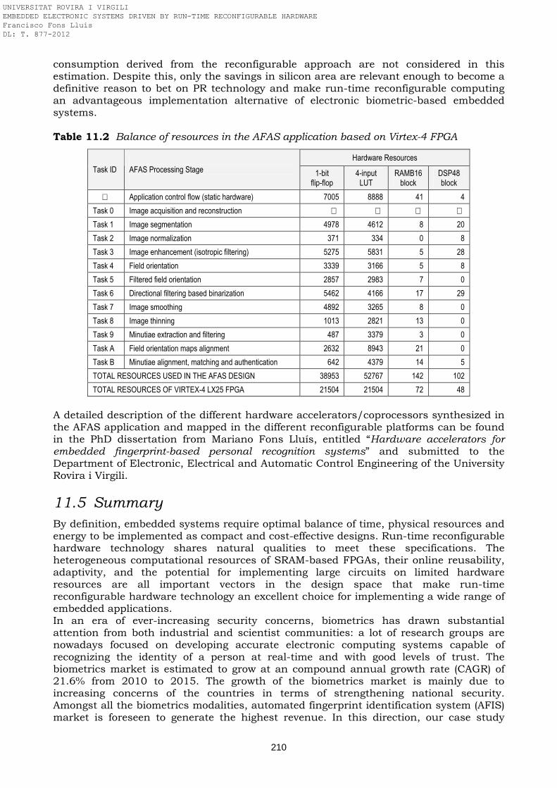
210
consumption derived from the reconfigurable approach are not considered in this estimation. Despite this, only the savings in silicon area are relevant enough to become a definitive reason to bet on PR technology and make run-time reconfigurable computing an advantageous implementation alternative of electronic biometric-based embedded systems. Table 11.2 Balance of resources in the AFAS application based on Virtex-4 FPGA
Hardware Resources Task ID
AFAS Processing Stage
1-bit flip-flop
4-input LUT
RAMB16 block
DSP48 block
Application control flow (static hardware) 7005 8888 41 4
Task 0 Image acquisition and reconstruction
Task 1 Image segmentation 4978 4612 8 20
Task 2 Image normalization 371 334 0 8
Task 3 Image enhancement (isotropic filtering) 5275 5831 5 28
Task 4 Field orientation 3339 3166 5 8
Task 5 Filtered field orientation 2857 2983 7 0
Task 6 Directional filtering based binarization 5462 4166 17 29
Task 7 Image smoothing 4892 3265 8 0
Task 8 Image thinning 1013 2821 13 0
Task 9 Minutiae extraction and filtering 487 3379 3 0
Task A Field orientation maps alignment 2632 8943 21 0
Task B Minutiae alignment, matching and authentication 642 4379 14 5
TOTAL RESOURCES USED IN THE AFAS DESIGN 38953 52767 142 102
TOTAL RESOURCES OF VIRTEX-4 LX25 FPGA 21504 21504 72 48
A detailed description of the different hardware accelerators/coprocessors synthesized in the AFAS application and mapped in the different reconfigurable platforms can be found in the PhD dissertation from Mariano Fons Lluís, entitled “Hardware accelerators for embedded fingerprint-based personal recognition systems” and submitted to the Department of Electronic, Electrical and Automatic Control Engineering of the University Rovira i Virgili.
11.5 Summary
By definition, embedded systems require optimal balance of time, physical resources and energy to be implemented as compact and cost-effective designs. Run-time reconfigurable hardware technology shares natural qualities to meet these specifications. The heterogeneous computational resources of SRAM-based FPGAs, their online reusability, adaptivity, and the potential for implementing large circuits on limited hardware resources are all important vectors in the design space that make run-time reconfigurable hardware technology an excellent choice for implementing a wide range of embedded applications. In an era of ever-increasing security concerns, biometrics has drawn substantial attention from both industrial and scientist communities: a lot of research groups are nowadays focused on developing accurate electronic computing systems capable of recognizing the identity of a person at real-time and with good levels of trust. The biometrics market is estimated to grow at an compound annual growth rate (CAGR) of 21.6% from 2010 to 2015. The growth of the biometrics market is mainly due to increasing concerns of the countries in terms of strengthening national security. Amongst all the biometrics modalities, automated fingerprint identification system (AFIS) market is foreseen to generate the highest revenue. In this direction, our case study
UNIVERSITAT ROVIRA I VIRGILI EMBEDDED ELECTRONIC SYSTEMS DRIVEN BY RUN-TIME RECONFIGURABLE HARDWARE Francisco Fons Lluís DL: T. 877-2012
211
encompasses fingerprint-based recognition. It is presented the design and development of a fingerprint image computer able to deploy all the typical processing stages involved in a classical biometric recognition algorithm. This work aims to be a best practice example of run-time partial reconfiguration for embedded applications. The concept of temporal partitioning of an application into tasks processed in a sequential order on a subset of shared resources of an FPGA fits well in the two technological disciplines involved in real-time embedded security: cryptography and biometric personal recognition. Both computing disciplines admit a temporal breakdown of serial or parallel tasks that can be processed in space on a shared region of an FPGA. On the one hand, cryptography has already been exploited through PR by the research community reaching good results, as presented in chapter 6. On the other hand, for the first time in the scientific community, it is proposed now to address the development of an automatic personal recognition system based on biometric features through run-time reconfigurable hardware technology, aimed at achieving a well-balanced price-performance trade-off. In this pioneer conception, the compute-intensive tasks of the biometric personal recognition algorithm are partitioned and synthesized first in a series of coprocessors that are then instantiated and executed multiplexed in time on a partially reconfigurable region of the FPGA. The implementation benchmark of the AFAS either as a pure software approach on a PC platform under a dual-core processor (Intel Core 2 Duo T5600 at 1.83 GHz) or as a reconfigurable FPGA co-design (identical algorithm partitioned in HW/SW tasks operating at 50 or 100 MHz on the second smallest device of the Xilinx Virtex-4 LX family) highlights a speed-up of one order of magnitude in favor of the FPGA alternative. The proposed FPGA-based architecture is able to handle a biometric recognition system at real-time. Specifically, the proposed architecture running at 50–100 MHz delivers a processing speed up of 16 in comparison to an instruction-set processor clocked at 1.83 GHz. Furthermore, this design strategy based on run-time reconfigurable computing allows to save an important amount of silicon area in contrast to the number of resources which would be needed in case of a traditional solution based on a static hardware implementation of the whole system (with all the hardware computers mapped on silicon at the same time and present for all the execution time), while still fulfilling stringent real-time characteristics demanded by this type of ergonomic applications. Thus, this work is a sensible demonstration that a high-demanding (time-critical) AFAS application can be embedded into a small and low-cost FPGA device. These results let point out biometric recognition as a sensible killer application for run-time reconfigurable computing, mainly in terms of efficiently balancing computational power, functional flexibility and cost. In this sense, the results of this work can leverage embedded biometric applications in the market to propel the implementation of highly efficient recognition algorithms at an affordable cost, fact that should definitively allow embedding them into many consumer applications or portable equipments and introduce thus run-time reconfigurable hardware technology in commercial products. The infallibility of the biometric recognition is today an open issue. The results of FAR 2.2% and FRR 2.2% obtained in the last edition of the Fingerprint Verification Competition (FVC 2006) prove that the state-of-the-art in algorithmics does not guarantee yet an error-free authentication/identification rate. In order to improve these figures, the complexity of the biometric algorithm seems will have to increase, fact that will lead to increase the processing power of the system intended to execute such computations. Many research groups from both academia and industria are joining efforts in search of the whole free-of-errors solution, fact that should help to increase the acceptance of these biometric systems in the society. This work proves the fact that PR technology is in a well position to contribute to the efficient implementation of biometric processing. The results obtained in this work let appoint run-time partial reconfiguration as a valid alternative to overcome the growing complexity of the embedded applications at low-cost, by simply translating the future new computational tasks that will probably require the applications into new hardware coprocessors to be processed on the same set
UNIVERSITAT ROVIRA I VIRGILI EMBEDDED ELECTRONIC SYSTEMS DRIVEN BY RUN-TIME RECONFIGURABLE HARDWARE Francisco Fons Lluís DL: T. 877-2012
212
of shared resources, just to not impact on system cost. Although there are many works published by the research community that disseminate the use of programmable logic (FPGA or SoC) devices to implement biometric algorithms, as far as the author knows, this work is the pioneer in spreading the use of run-time flexible hardware in the implementation of automatic personal recognition systems. The concept applied to fingerprints can also be extrapolated to multi-modal biometrics, where other physiological or behavioral features such as iris, face or voice can be processed over a partition of time-shared resources of a reconfigurable-programmable logic device to execute specific signal processing stages at real-time.
References
[Cheng and Tian, PRL 2004] J. Cheng, J. Tian, Fingerprint enhancement with dyadic scale-space, Pattern Recognition Letters, vol. 25, no. 11, p. 1273-1284, 2004.
[Danese et al., DSD 2009] G. Danese, M. Giachero, F. Leporati, G. Matrone, N. Nazzicari, An FPGA-based embedded system for fingerprint matching using phase-only correlation algorithm, Euromicro Conference on Digital System Design, Architectures, Methods and Tools, pp. 672-679, 2009.
[Danese et al., MICPRO 2011] G. Danese, M. Giachero, F. Leporati, N. Nazzicari, An embedded multi-core biometric identification system, Microprocessors and Microsystems, vol. 35, no. 5, pp. 510-521, 2011.
[Guo and Hall, ACM 1989] Z. Guo, W.R. Hall, Parallel thinning with two-subiteration algorithm, Communications of the ACM, vol. 32, no. 3, pp. 359-373, 1989.
[Hong et al., TPAMI 1998] L. Hong, Y. Wan, A. Jain, Fingerprint image enhancement: algorithm and performance evaluation, IEEE Transactions on Pattern Analysis and Machine Intelligence, vol. 20, no. 8, pp. 777-789, 1998.
[Jain et al., Computer 2010] A. K. Jain, J. Feng, K. Nandakumar, Fingerprint matching, IEEE Computer, February 2010.
[Jiang and Crookes, JRTIP 2008] R.M. Jiang, D. Crookes, FPGA-based minutia matching for biometric fingerprint image database retrieval, Journal of Real-Time Image Processing, vol. 3, no. 3, pp. 177-182, Springer-Verlag, 2008.
[Lam et al., TPAMI 1992] L. Lam, S. W. Lee, C.Y. Suen, Thinning methodologies. A comprehensive survey, IEEE Transactions on Pattern Analysis and Machine Intelligence, vol. 14, no. 9, pp. 869-885, 1992.
[Mainguet et al., ICBA 2004] J.F. Mainguet, W. Gong, A. Wang, Reducing silicon fingerprint sensor area, Proc. of the Int. Conference on Biometric Authentication, LNCS, vol. 3072, pp. 301-308, 2004.
[Ratha and Jain, TPDS 1999] N.K. Ratha, A.K. Jain, Computer vision algorithms on reconfigurable logic arrays, IEEE Transactions on Parallel and Distributed Systems, vol. 10, no. 1, pp. 29–43, 1999.
[Rao and Schunck, CVPR 1989] A. Ravishankar Rao, B.G. Schunck, Computing oriented texture fields, IEEE International Conference on Computer Vision and Pattern Recognition, pp. 61-68, 1989.
[Ratha et al., PR 1995] N.K. Ratha, S. Chen, A.K. Jain, Adaptive flow orientation-based feature extraction in fingerprint images, Pattern Recognition, vol. 28, no. 11, pp. 1657-1672, 1995.
[Ross et al., PR 2003] A. Ross, A. Jain, J. Reisman, A hybrid fingerprint matcher, Pattern Recognition, vol. 36, no. 7, pp. 1661-1673, 2003.
[Rodríguez et al., ARC 2006] D. Rodríguez, J.M. Sánchez, A. Duran, Mobile fingerprint identification using a hardware accelerated biometric service provider, Reconfigurable Computing: Architectures and Applications, LNCS, vol. 3985, pp. 383-388, Springer, 2006.
[Tico and Kuosmanen, TPAMI 2003] M. Tico, P. Kuosmanen, Fingerprint matching using an orientation-based minutia descriptor, IEEE Transactions on Pattern Analysis and Machine Intelligence, vol. 25, no. 8, pp. 1009-1014, 2003.
[Wakahara et al., SCJ 2007] T. Wakahara, Y. Kimura, A. Suzuki, A. Shio, M. Sano, Fingerprint verification using ridge direction distribution and minutiae correspondence, Journal Systems and Computers in Japan, vol. 28, no. 3, pp. 72–82, 2007.
UNIVERSITAT ROVIRA I VIRGILI EMBEDDED ELECTRONIC SYSTEMS DRIVEN BY RUN-TIME RECONFIGURABLE HARDWARE Francisco Fons Lluís DL: T. 877-2012
213
Chapter 12 Automotive electronic control unit Nowadays, the use of electronics is the basis for introducing competitive advantages in the automobile industry. Leading companies must constantly innovate by providing new end-user functionality, typically synthesized in hardware and software in the way of electronic control units (ECUs). On the one hand the escalating competition among cars manufacturers to offer exclusive technological features to their customers and, on the other hand, the strict safety and environmental regulations imposed by the legislation have led to the explosive growth of the automotive electronics industry. In this scenario, AUTOSAR (Automotive Open System Architecture) and Functional Safety (ISO 26262) standards are today the two hottest topics in the automotive field which articulate the technical and architectural bases of design of ECUs. At the same time as the automotive electronics density increases to satisfy the growing functional demand for new vehicles, FPGA manufacturers are delivering bigger devices –capable already of integrating a full embedded application inside– at a more competitive price. This trend makes feasible the expansion of reconfigurable computing technology in the automotive industry. In this direction, the author addresses in this chapter a pioneering approach to architect an automotive ECU on a programmable logic device deploying both AUTOSAR and ISO 26262 standards. The author highlights the advantages of synthesizing an AUTOSAR-compliant ECU provided with safety-related functions on a SoC/FPGA instead of on a typical single-core/dual-core MCU. Hence, this work spreads a computing paradigm change based on the replacement of a software-only solution by an alternative driven by hardware/software co-design and reconfigurable computing techniques in specific ECU scenarios where a purely sofware approach is not feasible due to performance-complexity reasons.
12.1 Introduction
Due to the growing electronic content of vehicles, the automotive industry is expected to become increasingly important to semiconductor manufacturers. Analysts predict that the market for semiconductors in automotive applications will increase at a CAGR of 8% in the coming five years. One of the fastest-growing segments relates to MCUs and FPGAs. This would come as a result of the wide range and greater number of emerging applications for motor vehicles, including safety and driver assistance, car-to-car communications, driver monitoring, comfort and control functions, navigation systems, entertainment and the popular spectrum of hybrid-electric technologies. In such a landscape, the evolution of automotive electronics is expanding at a rapid rate and the automobile has been transformed from a primarily electro-mechanical device into an integrated machine controlled by electronics, with embedded hardware and software in all its major subsystems, including engine control, power train, energy management, body functions and infotainment. The computational power present in a vehicle is today distributed through ECUs interconnected via several communication networks. In modern cars, one can find more than 70 ECUs which manage lots of embedded functions like fuel injection, anti-lock braking system (ABS) or battery state-of-charge/state-of-health monitoring, to name just a few. Automotive leading manufacturers realized soon the unavoidable need to address the growing complexity of designing and managing automotive systems in an effective way. Today and also in the future, both AUTOSAR and ISO 26262 standards constraint the way hardware and software systems are architected, designed, developed and deployed in real automotive ECUs.
UNIVERSITAT ROVIRA I VIRGILI EMBEDDED ELECTRONIC SYSTEMS DRIVEN BY RUN-TIME RECONFIGURABLE HARDWARE Francisco Fons Lluís DL: T. 877-2012

214
12.1.1 AUTOSAR
AUTOSAR is an initiative conducted by the automobile industry that represents a step forward towards the definition of a standard system architecture for the electronic control units distributed in vehicles. It is a partnership of manufacturers and suppliers working together to develop and establish a de-facto open industry standard for automotive electrical/electronic (E/E) architectures. From a technical point of view, several major issues are intended to be addressed: manage the growing complexity of automotive E/E systems associated with the continuous increase of functionality; improve flexibility for product modification, upgrade and update; improve scalability of solutions within and across product lines; improve quality and reliability of E/E systems; and enable detection of errors in early design phases. Since 2003, this development partnership of car manufacturers, suppliers and other companies from the electronics, semiconductor and software industry have been working on the basis for reliably controlling the growing complexity of the E/E systems in motor vehicles, as well as improving cost efficiency without compromising quality. The core partners of AUTOSAR are the BMW Group, Bosch, Continental, Daimler, Ford, General Motors, PSA Peugeot Citroën, Toyota and the Volkswagen Group. In addition to these companies, more than 160 members play an important role in the success of the partnership. Their common objective is to create a basis for industry collaboration on basic functions while providing a platform which continues to encourage competition on innovative functions. Under the slogan “cooperate on standards, compete on implementation”, automotive manufacturers and suppliers work together to develop and establish an open industry standard aimed at being a breakthrough in automotive E/E design (http://www.autosar.org).
12.1.2 ISO 26262
During the last years, mechanical components within vehicles have been more and more displaced by electronic components which are taking over additional control, monitoring and diagnostic functions. These higher levels of complexity together with shorter product development cycles result in product failures. Functional safety turns out to be one of the key issues of present and future automobile development as new safety-critical functions increasingly emerge. Since August 2004, the International Electrotechnical Commission’s IEC 61508 is a master, accepted worldwide standard for functional safety of electrical, electronic and programmable electronic (E/E/PE) safety-related systems and components. It contains a generic solution for all activities during the safety life cycle of E/E/PE equipment that is performing safety functions. Based on the various fields of application of all these safety-related systems, tailored standards have been established. Among them, the International Organization for Standardization's ISO 26262 is an adaptation of the IEC 61508 for automotive E/E systems, in place since the end of 2011. It is a regulation that provides the automotive industry with support for the safe development of automotive software and hardware system architectures. The entire D&D life cycle is thus governed by standards that demand systematic processes. The bases of functional safety are the avoidance of faults (e.g. systematic software faults) or the detection and handling of faults (e.g. random hardware faults) in order to mitigate their effects and thus prevent the violation of any established safety goal. The basic idea behind reducing risk emanating from vehicle systems is that based on the severity of possible accidents, the probability of exposure to certain driving situation and the risk reduction due to external measures, an automotive safety integrity level (ASIL) is defined which, in case that all requirements are satisfied, reduces the intolerable risk to a tolerable residual risk. In this context, the term risk is defined as the combination of the probability of a harm/damage occurring and its severity, and during the engineering development phase all potential hazards and risks shall be assessed in advance and take suitable measures to minimize them.
UNIVERSITAT ROVIRA I VIRGILI EMBEDDED ELECTRONIC SYSTEMS DRIVEN BY RUN-TIME RECONFIGURABLE HARDWARE Francisco Fons Lluís DL: T. 877-2012
215
This standard is aligned to automotive industry use cases and definitions of acceptable risks and intends to prevent failures that could result in a catastrophe. Manufacturers as well as suppliers need to prove to their customers and accreditation authorities that despite increasing complexity and software determination their electronic systems will deliver the required functionality safely and reliably, according to industry-specific regulations (http://www.iso.org/iso/).
12.2 Related work
Recently, the automotive sector has been working actively in defining the design rules of the automobile of the future driven by AUTOSAR and ISO 26262 standards. At the same time that these standards have been defined, the semiconductor companies have worked hard to launch new devices adapted to these new requirements. In this direction, suppliers of microcontrollers like STMicroelectronics or Freescale Semiconductor have jointly develop new families of MPC560/SPC560 processors based on a PowerPC architecture and adapted to the AUTOSAR demands, as well as keeping specific reliability/safety functions implemented in hardware like memory protection units (MPU) and error correction codes (ECC). In parallel, Texas Instruments Inc. has introduced the automotive TMS570 microcontroller, an ARM Cortex-R4F lock step dual-core processor specifically designed to meet the IEC 61508 SIL3 or ISO 26262 ASIL D safety levels. A similar approach has been conducted by Freescale Semiconductor with its Leopard MPC564xL MCU composed of a dual-core PowerPC processor admitting both lock step and dual parallel modes, certified according to IEC 61508 SIL3 and equipped with core hardware enhancements for self-test, redundant computation mechanisms, MPUs, redundant voltage monitor, ECC on all memories, etc. Other companies focused on the development of embedded software have developed their solutions to offer AUTOSAR-based applications with safety-related functions certified to specific ASIL levels, like Vector Informatik GmbH and its MICROSAR Safe solution, containing safety integrity functions such as program flow monitoring for safety-related SWCs, reliable intra- and inter-ECU communication, periodic hardware checking during operation, and so on. Other initiatives are research projects. The DysCAS (dynamically self-configuring automotive systems) project, funded by the Sixth Framework Programme (FP6) of the European Commission and composed of partners from both academia and industry –including automakers like Volvo Technology AB and Daimler AG– targets the self-configuration of automotive embedded systems. The main work of the project has been the development of a reference middleware architecture that, unlike the common static design-time configurations, is able to adapt itself after its production –in driving, stand-still or in the dealer– to changing internal and external conditions. In the project, corresponding middleware implementations have been realized based on several different real-time operating systems, networks and processors. The main result is the reference architecture which provides sophisticated capabilities to configure itself in context-aware ways to meet the quality-of-service requirements of applications, to automatically optimize resource usage, and to dynamically detect and resolve certain categories of faults. In this way, the DySCAS project, although mainly oriented to infotainment applications, represents a first step towards self-managing automotive systems [Anthony et al., EIK 2006]. Up to now, it has been overviewed approaches based on MCUs. On the other extreme, the use of programmable logic oriented to take part in AUTOSAR and functional safety solutions has been also promoted by other groups. In the field of FPGA-based ECU designs in the automotive industry based on programmable logic, many FPGA suppliers like Xilinx and Altera have qualified devices for automotive applications. Most of these devices are used across driver assistance, driver information and infotainment systems. Besides, EDA tools providers like Mathworks show interest for this field [Sharma and Chen, SAE 2009]. As example of functional safety deployment on FPGAs, TÜV Rheinland
UNIVERSITAT ROVIRA I VIRGILI EMBEDDED ELECTRONIC SYSTEMS DRIVEN BY RUN-TIME RECONFIGURABLE HARDWARE Francisco Fons Lluís DL: T. 877-2012
216
–a company dedicated to technical safety services and consulting– qualified the FPGA design methodology and tools of Altera aimed at enabling the implementation of FPGA-based safety-related systems. This FPGA-based design methodology allows FPGA users to design their own customized safety controllers and provides a significant competitive advantage over traditional MCU- or ASIC-based designs concerning flexibility and simplicity in complex safety systems [Altera Corp., WP01123 2010]. Besides, in [Salewski and Kowalewski, TII 2008] a comparison of MCUs and FPGAs with respect to safety and reliability properties is presented. With regard to the handling of hardware faults, no major differences are identified between those two hardware platforms, therefore there is not any technical obstacle or stopper in the use of FPGA technology in automotive safety-critical applications. In [Conmy and Bate, TII 2010], it is shown how a modular design embedded on an FPGA can be exhaustively analyzed from a safety perspective. It traces very low-level FPGA faults to high-level system hazards. This is achieved by performing exhaustive bottom-up failure analysis of the FPGA circuit to determine how potentially hazardous outputs can occur at the I/O pins of the FPGA device. A hierarchical component-based approach is then used to manage scale. Concerning automotive applications based on FPGA devices used as static hardware designs, in [Hong-qiang et al., ICVES 2007] it is designed a door module ECU that integrates a window lifter controller with anti-trap protection. The whole system is embedded in an Altera Stratix EP1S40 FPGA composed of a soft-core 8051 CPU and a CAN controller, both described in VHDL. In the area of FPGA-based automotive applications exploiting dynamic reconfiguration, not too many initiatives have been conducted up to now. Within the research project ReCoNets [Teich et al., DATE 2006], concepts like self-adaptation and fault-tolerance in automotive control architectures are addressed by bringing FPGA reconfiguration in ECUs. The idea proposed consists in allowing the reallocation of functionality in hardware or software in case of detecting ECU faults to repair quickly the fault and reach a proper balance of computational load among functional nodes. As proof-of-concept, this approach is demonstrated in a self-adaptive driver assistance system. In another work, Toyota evaluates the use of FPGA dynamic reconfiguration for reaching fail-safe ECU systems [Chujo, TCRDL 2002]. An FPGA-based subsystem is configured to monitor and detect failures under normal operation conditions. If a fault is detected, the FPGA is dynamically reconfigured to be a backup circuit to the faulty control circuit. The proof of feasibility is conducted in a Xilinx 6216 FPGA. Still another use case, in [Becker et al., IEEE 2007], the University of Karlsruhe and Daimler AG worked together on a cooperative research project concerning the usage of dynamic and partially reconfigurable hardware for automotive applications. The project is oriented to the design of an automotive ECU concept implemented in a run-time reconfigurable FPGA platform. The proof of concept, applied to a body controller ECU responsible for the control of actuators like window lifters, seats or rear mirrors, shows that dynamically reconfigurable FPGAs can be exploited to reduce power dissipation and increase the adaptivity of such embedded systems. Concerning AUTOSAR and reconfigurable computing, the work carried out by Pham et al. focuses on assuring fault-tolerant communication among automotive ECUs by the use of FPGA dynamic partial reconfiguration, integrating this approach inside the AUTOSAR system architecture [Pham et al., ITST 2009]. The proof of feasibility is based on the use of FlexRay and CAN standard communication protocols. They propose a method for switching from one bus to another if some error occurs in one of them. In that case, the change of communication protocol is performed by reconfiguring the communication IP. For this, the ECU is prototyped in a Xilinx Virtex-5 XC5VSX50T FPGA provided with a PR region where it is placed the partition of the COM stack that can be reconfigured on the fly. In order to integrate the partial reconfiguration into the AUTOSAR architecture, it is exploited the post-build AUTOSAR attribute. Although this application example is applied only to a minor part of the ECU system, it is an early concept about integrating a dynamically reconfigurable architecture in AUTOSAR environments.
UNIVERSITAT ROVIRA I VIRGILI EMBEDDED ELECTRONIC SYSTEMS DRIVEN BY RUN-TIME RECONFIGURABLE HARDWARE Francisco Fons Lluís DL: T. 877-2012
217
Now, aimed at going one step further in the spread of reconfigurable computing in the automotive industry, the work proposed in this chapter describes the use of FPGA hardware resources to complement the AUTOSAR architecture originated for a MCU device with new standard and custom peripherals –implemented in reconfigurable hardware– that make easier and more flexible the design of an ECU system, including furthermore the deployment of safety components derived from the implementation of the ISO 26262 standard, and synthesizing all these components either in hardware or in software depending on the specific functional requirements demanded. Like this, the approach presented in the next sections, although it is only an early concept, is pioneer in terms of merging both AUTOSAR and functional safety with run-time reconfigurable hardware to implement a full automotive ECU embedded system. In fact, although today reconfigurable hardware is not covered in AUTOSAR, this possibility can not be discarded in the future. A clear example of this assumption is for instance the fact that run-time reconfigurable hardware is already used in aerospace applications, and the automotive field has been following and adopting, in many aspects and during many occasions in the past, the trends put in practice previously in the aerospace field.
12.3 System architecture
As introduced in the previous sections, this chapter addresses an open issue highlighted from time ago by automakers regarding the increasing system complexity in the automobile and the need for handling this complexity in an effective way. Automotive manufacturers face the challenge of having to integrate a growing amount of software, mechanical and electronic technologies across a vast ecosystem of suppliers. AUTOSAR and ISO 26262 directives are mainly led from a software development perspective and oriented to computing platforms based on microcontroller units. However, the inclusion of hardware/software co-design and reconfigurable computing techniques can bring some advantages in this landscape. While nowadays standard MCUs are the dominant hardware platform in automotive ECUs, as price for programmable logic devices come down, the FPGA/SoC devices are seeing broader acceptance in the automotive markets. That is particularly true in the infotainment sector today, where high speeds for digital-signal processing are opening doors for the technology. This work aims to put together all the advantages of use of reconfigurable hardware in automotive applications. For this, the author describes in this chapter the potential of this technology through a use case oriented to one of the most important ECUs found in the automobile concerning deployment of end-user functions: a body control module or BCM. Important reasons support this innovative approach, as expounded next.
12.3.1 Real scenario
The standardization of the ECU architecture proposed by AUTOSAR is necessary in order to manage the increasing functional complexity in a cost-efficient way. It enables a high integration of functions and the reusability of software components or applications. The main goal of AUTOSAR is to define a uniform software architecture for ECUs and decouple the hardware from the software. Like this, AUTOSAR promotes the reuse of software by defining interfaces that are hardware independent, that is, a software component that has been written in accordance with the AUTOSAR standard should work on any vendor’s microcontroller provided it has been properly integrated into an AUTOSAR-compliant run-time environment (RTE). This fact delivers increased flexibility to the automaker, which can exchange the same software modules developed by different suppliers in a transparent way, thanks to its plug and play characteristics, and without affecting the behavior of the vehicle. Thus, hardware and software reach to be widely independent of each other. This decoupling is achieved by means of a system architecture composed of software layers. Figure 12.1 shows the system architecture promoted by AUTOSAR decomposed in functional layers.
UNIVERSITAT ROVIRA I VIRGILI EMBEDDED ELECTRONIC SYSTEMS DRIVEN BY RUN-TIME RECONFIGURABLE HARDWARE Francisco Fons Lluís DL: T. 877-2012
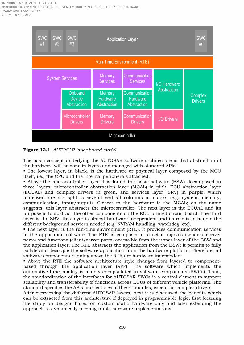
218
Figure 12.1 AUTOSAR layer-based model The basic concept underlying the AUTOSAR software architecture is that abstraction of the hardware will be done in layers and managed with standard APIs: The lowest layer, in black, is the hardware or physical layer composed by the MCU itself, i.e., the CPU and the internal peripherals attached. Above the microcontroller layer it is found the basic software (BSW) decomposed in three layers: microcontroller abstraction layer (MCAL) in pink, ECU abstraction layer (ECUAL) and complex drivers in green, and services layer (SRV) in purple, which moreover, are are split is several vertical columns or stacks (e.g. system, memory, communication, input/output). Closest to the hardware is the MCAL; as the name suggests, this layer abstracts the microcontroller. The next layer is the ECUAL and its purpose is to abstract the other components on the ECU printed circuit board. The third layer is the SRV; this layer is almost hardware independent and its role is to handle the different background services needed (e.g. NVRAM handling, watchdog, etc). The next layer is the run-time environment (RTE). It provides communication services to the application software. The RTE is composed of a set of signals (sender/receiver ports) and functions (client/server ports) accessible from the upper layer of the BSW and the application layer. The RTE abstracts the application from the BSW; it permits to fully isolate and decouple the software application from the hardware platform. Therefore, all software components running above the RTE are hardware independent. Above the RTE the software architecture style changes from layered to component-based through the application layer (APP). The software which implements the automotive functionality is mainly encapsulated in software components (SWCs). Thus, the standardization of the interfaces for AUTOSAR SWCs is a central element to support scalability and transferability of functions across ECUs of different vehicle platforms. The standard specifies the APIs and features of these modules, except for complex drivers. After overviewing the different AUTOSAR layers, next it is discussed the benefits which can be extracted from this architecture if deployed in programmable logic, first focusing the study on designs based on custom static hardware only and later extending the approach to dynamically reconfigurable hardware implementations.
Run-Time Environment (RTE)
Microcontroller
Complex Drivers
I/O Hardware Abstraction
I/O Drivers
Communication Services
Communication Drivers
Communication Hardware
Abstraction
Memory Services
Memory Drivers
Memory Hardware
Abstraction
Microcontroller Drivers
Onboard Device
Abstraction
System Services
Application Layer
SWC
#1
SWC
#2
SWC
#3
SWC
#n
UNIVERSITAT ROVIRA I VIRGILI EMBEDDED ELECTRONIC SYSTEMS DRIVEN BY RUN-TIME RECONFIGURABLE HARDWARE Francisco Fons Lluís DL: T. 877-2012
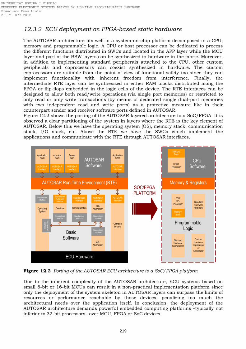
219
12.3.2 ECU deployment on FPGA-based static hardware The AUTOSAR architecture fits well in a system-on-chip platform decomposed in a CPU, memory and programmable logic. A CPU or host processor can be dedicated to process the different functions distributed in SWCs and located in the APP layer while the MCU layer and part of the BSW layers can be synthesized in hardware in the fabric. Moreover, in addition to implementing standard peripherals attached to the CPU, other custom peripherals and coprocessors can coexist synthesized in hardware. The custom coprocessors are suitable from the point of view of functional safety too since they can implement functionality with inherent freedom from interference. Finally, the intermediate RTE layer can be synthesized in either RAM blocks distributed along the FPGA or flip-flops embedded in the logic cells of the device. The RTE interfaces can be designed to allow both read/write operations (via single port memories) or restricted to only read or only write transactions (by means of dedicated single dual-port memories with two independent read and write ports) as a protective measure like in their counterpart sender and receiver software ports defined in AUTOSAR. Figure 12.2 shows the porting of the AUTOSAR-layered architecture to a SoC/FPGA. It is observed a clear partitioning of the system in layers where the RTE is the key element of AUTOSAR. Below this we have the operating system (OS), memory stack, communication stack, I/O stack, etc. Above the RTE we have the SWCs which implement the applications and communicate with the RTE through AUTOSAR interfaces. Figure 12.2 Porting of the AUTOSAR ECU architecture to a SoC/FPGA platform Due to the inherent complexity of the AUTOSAR architecture, ECU systems based on small 8-bit or 16-bit MCUs can result in a non-practical implementation platform since only the deployment of the system skeleton in AUTOSAR layers can surpass the limits of resources or performance reachable by those devices, penalizing too much the architectural needs over the application itself. In conclusion, the deployment of the AUTOSAR architecture demands powerful embedded computing platforms –typically not inferior to 32-bit processors– over MCU, FPGA or SoC devices.
Basic Software
AUTOSAR Software
Application
SWC
AUTOSAR Interface
Application
SWC
AUTOSAR Interface
Actuator
SWC
AUTOSAR Interface
Sensor SWC
AUTOSAR Interface
AUTOSAR Run-Time Environment (RTE)
AUTOSAR Interface
Programmable Logic
CPU Software
Memory & Registers
BSW CPU
Processor
Standard Hardware
Coprocessor
Memory Block
HOST
Processor
Memory Block
Custom
Hardware Coprocessor
or Accelerator
Standard Hardware Peripheral
ECU
Abstraction
AUTOSAR Interface
Standardized Interface
MCU
Abstraction
Standardized Interface
Operating System
Standardized Interface
Communication
Standardized Interface
Standardized Interface
Services
Standardized AUTOSAR Interface
Standardized Interface
Complex Drivers
ECU-Hardware
Standardized interface
SOC/FPGA PLATFORM
UNIVERSITAT ROVIRA I VIRGILI EMBEDDED ELECTRONIC SYSTEMS DRIVEN BY RUN-TIME RECONFIGURABLE HARDWARE Francisco Fons Lluís DL: T. 877-2012
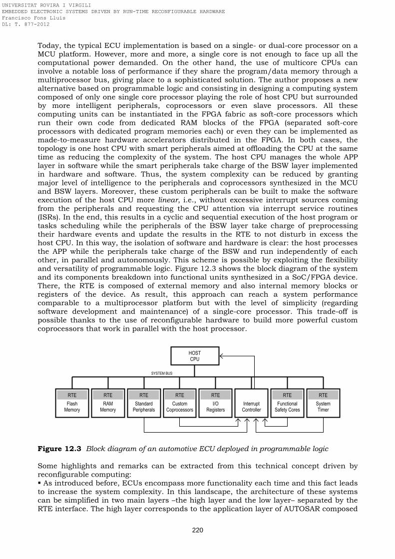
220
Today, the typical ECU implementation is based on a single- or dual-core processor on a MCU platform. However, more and more, a single core is not enough to face up all the computational power demanded. On the other hand, the use of multicore CPUs can involve a notable loss of performance if they share the program/data memory through a multiprocessor bus, giving place to a sophisticated solution. The author proposes a new alternative based on programmable logic and consisting in designing a computing system composed of only one single core processor playing the role of host CPU but surrounded by more intelligent peripherals, coprocessors or even slave processors. All these computing units can be instantiated in the FPGA fabric as soft-core processors which run their own code from dedicated RAM blocks of the FPGA (separated soft-core processors with dedicated program memories each) or even they can be implemented as made-to-measure hardware accelerators distributed in the FPGA. In both cases, the topology is one host CPU with smart peripherals aimed at offloading the CPU at the same time as reducing the complexity of the system. The host CPU manages the whole APP layer in software while the smart peripherals take charge of the BSW layer implemented in hardware and software. Thus, the system complexity can be reduced by granting major level of intelligence to the peripherals and coprocessors synthesized in the MCU and BSW layers. Moreover, these custom peripherals can be built to make the software execution of the host CPU more linear, i.e., without excessive interrupt sources coming from the peripherals and requesting the CPU attention via interrupt service routines (ISRs). In the end, this results in a cyclic and sequential execution of the host program or tasks scheduling while the peripherals of the BSW layer take charge of preprocessing their hardware events and update the results in the RTE to not disturb in excess the host CPU. In this way, the isolation of software and hardware is clear: the host processes the APP while the peripherals take charge of the BSW and run independently of each other, in parallel and autonomously. This scheme is possible by exploiting the flexibility and versatility of programmable logic. Figure 12.3 shows the block diagram of the system and its components breakdown into functional units synthesized in a SoC/FPGA device. There, the RTE is composed of external memory and also internal memory blocks or registers of the device. As result, this approach can reach a system performance comparable to a multiprocessor platform but with the level of simplicity (regarding software development and maintenance) of a single-core processor. This trade-off is possible thanks to the use of reconfigurable hardware to build more powerful custom coprocessors that work in parallel with the host processor. Figure 12.3 Block diagram of an automotive ECU deployed in programmable logic Some highlights and remarks can be extracted from this technical concept driven by reconfigurable computing: As introduced before, ECUs encompass more functionality each time and this fact leads to increase the system complexity. In this landscape, the architecture of these systems can be simplified in two main layers –the high layer and the low layer– separated by the RTE interface. The high layer corresponds to the application layer of AUTOSAR composed
SYSTEM BUS
HOST CPU
Flash Memory
RAM Memory
Standard Peripherals
Custom Coprocessors
I/O Registers
Interrupt Controller
System Timer
Functional Safety Cores
RTE
RTE
RTE
RTE
RTE
RTE
RTE
UNIVERSITAT ROVIRA I VIRGILI EMBEDDED ELECTRONIC SYSTEMS DRIVEN BY RUN-TIME RECONFIGURABLE HARDWARE Francisco Fons Lluís DL: T. 877-2012
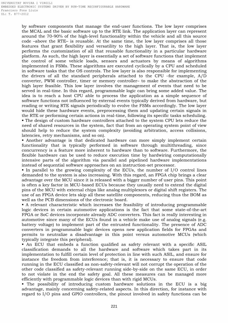
221
by software components that manage the end-user functions. The low layer comprises the MCAL and the basic software up to the RTE link. The application layer can represent around the 70-90% of the high-level functionality within the vehicle and all this source code –above the RTE– is reusable. At the same time, the low layer comprises all those features that grant flexibility and versatility to the high layer. That is, the low layer performs the customization of all that reusable functionality in a particular hardware platform. As such, the high layer is essentially a set of software functions that implement the control of some vehicle loads, sensors and actuators by means of algorithms implemented in FSMs. These algorithms are executed cyclically by a CPU and scheduled in software tasks that the OS controls. The low layer is also responsible for implementing the drivers of all the standard peripherals attached to the CPU –for example, A/D converter, PWM controller, timer or memory controller– to make the abstraction of the high layer feasible. This low layer involves the management of events that need to be served in real-time. In this regard, programmable logic can bring some added value. The idea is to reach a host CPU able to process the application as a simple sequence of software functions not influenced by external events typically derived from hardware, but reading or writing RTE signals periodically to evolve the FSMs accordingly. The low layer would hide these hardware events, preprocessing them and updating certain signals in the RTE or performing certain actions in real-time, following its specific tasks scheduling. The design of custom hardware controllers attached to the system CPU lets reduce the need of shared resources in the system, fact that from an operating system point of view should help to reduce the system complexity (avoiding arbitration, access collisions, latencies, retry mechanisms, and so on). Another advantage is that dedicated hardware can more simply implement certain functionality that is typically performed in software through multithreading, since concurrency is a feature more inherent to hardware than to software. Furthermore, the flexible hardware can be used to reduce execution time by hardwiring computationally intensive parts of the algorithm via parallel and pipelined hardware implementations instead of sequential software approaches on an instruction-set processor. In parallel to the growing complexity of the ECUs, the number of I/O control lines demanded to the system is also increasing. With this regard, an FPGA chip brings a clear advantage over the MCU since it is released with a bigger number of user pins. This point is often a key factor in MCU-based ECUs because they usually need to extend the digital pins of the MCU with external chips like analog multiplexors or digital shift registers. The use of an FPGA device lets skip all these satellite components, reducing thus the BOM as well as the PCB dimensions of the electronic board. A relevant characteristic which increases the feasibility of introducing programmable logic devices in certain automotive applications is the fact that some state-of-the-art FPGA or SoC devices incorporate already ADC converters. This fact is really interesting in automotive since many of the ECUs found in a vehicle make use of analog signals (e.g. battery voltage) to implement part of the entrusted functionality. The presence of ADC converters in programmable logic devices opens new application fields for FPGAs and permits to neutralize a disadvantage in this point versus automotive MCUs (which typically integrate this peripheral). An ECU that embeds a function qualified as safety relevant with a specific ASIL classification demands to all the hardware and software which takes part in its implementation to fulfill certain level of protection in line with such ASIL, and ensure for instance the freedom from interference; that is, it is necessary to ensure that code running in the ECU classified as non-safety-relevant will not corrupt the operation of the other code classified as safety-relevant running side-by-side on the same ECU, in order to not violate in the end the safety goal. All these measures can be managed more efficiently with programmable logic devices than with rigid MCUs. The possibility of introducing custom hardware solutions in the ECU is a big advantage, mainly concerning safety-related aspects. In this direction, for instance with regard to I/O pins and GPIO controllers, the pinout involved in safety functions can be
UNIVERSITAT ROVIRA I VIRGILI EMBEDDED ELECTRONIC SYSTEMS DRIVEN BY RUN-TIME RECONFIGURABLE HARDWARE Francisco Fons Lluís DL: T. 877-2012
222
grouped in made-to-measure I/O ports accessed exclusively by safety components inside the ECU. This approach permits to decouple the safety-critical pins from the non-safety-critical pins of the system, assuring the intended freedom from interference by design. This idea is depicted in Figure 12.4. Besides, the size of each GPIO port can be designed at the measure of the SWC which manages it. In this way, each application managed by a different SWC (e.g. window lifter, wiper/washer, etc) could have its specific port mapped in specific registers within the system memory map. In MCUs this is not possible since their ports have a fixed size (typically 8, 16 or 32 bits wide) and are addressed in a word-wise mode, not bit-wise, therefore it becomes a shared resource accessed by several SWCs at the same time. This strategy applied to a GPIO controller can be extended to other standard peripherals too (e.g. PWM controllers, ADC converters, etc).
Figure 12.4 HW/SW co-design of a safety architecture that isolates the safety-relevant ports from non-safety ports to guarantee the freedom from interference
The same decoupling strategy disclosed above for MCU standard peripherals can be applied to all the safety channels or data paths of a safety function. A typical way of implementating a certain ASIL necessary to reach a defined safety goal is by means of the ASIL decomposition strategy: a high level ASIL like C or D can be decomposed in redundant partitions of lower ASIL level so that each of these parts performed in duplicate is then implemented according to its new level. This safety strategy based on redundancy is a sensible argument for recurring to hardware, where several identical processing engines can be instantiated multiple times in the same programmable logic device. Moreover, the fulfilment of certain ASIL level is always clearer to prove with architectural approaches (hardware) than by means of software functionality. Other characteristic derived from the flexibility of programmable logic and applicable to functional safety is the possibility of implementing triple module redundancy (TMR) strategies. This is a commonly known method for single event upsets (SEU) mitigation. Such scheme involves three identical logic circuits performing the same task in parallel and with the corresponding outputs being compared through a majority voter circuit, being this strategy implemented very efficiently in hardware. A convincing advantage in the introduction of reconfigurable hardware in automotive ECUs is the fact that SoC/FPGA devices lets introduce this hardware feature progressively in a design. That is, the developer can design the system in software like typically would do for a MCU-based platform and then do the porting of certain parts originally implemented in software to hardware on the programmable logic resources. This methodology enables the designer to build different versions of a solution and realize the advantages of synthesizing some functions in custom hardware with respect to a purely software-based approach.
RTE
GPIO registers
BSW
oen out in
RTE
GPIO registers
BSW
oen out in
SAFETY SHELL
SAFETY-RELATED PATH
SW
HW
UNIVERSITAT ROVIRA I VIRGILI EMBEDDED ELECTRONIC SYSTEMS DRIVEN BY RUN-TIME RECONFIGURABLE HARDWARE Francisco Fons Lluís DL: T. 877-2012
223
12.3.3 ECU deployment on run-time reconfigurable hardware
After exploring the advantages of implementing ECUs in static hardware and software via programmable logic, some additional advantages are enumerated next in case that such solution exploits run-time partial reconfiguration technology. One advantage of run-time partially reconfigurable FPGAs against static FPGA designs is the fact that the startup time of the system can be reduced if the FPGA is composed of some PR regions that do not need to be configured at startup, for instance when the ECU wakes up. FPGAs which do not support active reconfiguration have to configure the whole FPGA resources at power up and this implies a considerable configuration latency to download the full bitstream. This latency can be notoriously reduced in systems based on big FPGAs equipped with run-time partial reconfiguration technology. In that case, it is possible to configure only the minimalist system at power up and initialize the rest of the system later when required. This startup process split in two phases lets speed up the initialization in case the system needs a fast response at power up or wakeup. Besides, if PRR regions are disabled, then it is possible to reduce the power consumption of the device. Power-saving modes are especially relevant in automotive battery-powered ECUs. For this reason, automotive MCUs make use of low-power modes to keep the ECU power consumption to a minimum when the vehicle is inactive (that is, in sleep mode). Analogously, the use of blank bitstreams to disable portions of the FPGA when not required reduces logic activity and consequently, dynamic power consumption. Inherited from the aerospace application field, the scrubbing technique can be used in automotive to recover the system in case of detecting failures on SRAM resources originated by SEU. By means of periodically reconfiguring the hardware peripherals it is guaranteed that in case of a malfunction the system is self-repaired and the maximum time the malfunction is present is restricted to the scrubbing period. Another promising feature coming from the flexibility of run-time partial reconfigurable technology is the fault recovery by means of function relocation in case of permanent or non-repairing circuit failures. Once a hardware or software fault has been identified, it is possible to automatically relocate the required functionality to another part of the programmable logic device inside the same ECU or even in another ECU. The most powerful characteristic of reconfigurable computing technology applicable in the automotive sector is, beyond doubt, the time-multiplexing of functionality on shared hardware resources on the fly. Time-sharing of functional applications processed in the same computing resources inside an ECU if these applications are mutually exclusive (for example, deployment of a lane-departure warning while a vehicle is running straight ahead and switching to a rear-camera view or park-assistance application when it is backing up) is an idea that could help to reduce the cost and complexity of such embedded systems, as well as freeing space and reducing weight in the vehicle. Porting the previous concept to its extreme, it is possible to envision a universal automotive ECU that is configured in the manufacturing line to customize it to a specific ECU for a specific automobile platform. This idea, technically feasible through reconfigurable hardware, would simplify to the minimum the stocks and logistics in the manufacturing plants since the module assembled in the production line from the hardware point of view would be the same for all the vehicle platforms, only the software or bitstream would change to make the ECU functional differentiation.
12.4 Summary
Nowadays, around 90 percent of innovation in the automotive sector is nowadays driven by electronics, and there is no end in sight. While in-vehicle functions grow in number and complexity, it is expected that the car of the future will be based on very advanced embedded software and hardware technologies. Moreover, controlling the cost of automotive embedded systems is extremely important for automobile suppliers competing in a very high-volume industry. As a result, one approach shared by many
UNIVERSITAT ROVIRA I VIRGILI EMBEDDED ELECTRONIC SYSTEMS DRIVEN BY RUN-TIME RECONFIGURABLE HARDWARE Francisco Fons Lluís DL: T. 877-2012
224
OEMs in the automobile industry is to reduce the number of ECUs present in the vehicle in exchange for delivering major functionality per unit. This is a goal that demands more powerful computing platforms, creating highly integrated ECUs as domain controllers aimed at reducing the system complexity. Besides, new design constraints have been inherited from the recent introduction of the AUTOSAR and ISO 26262 standards. All these trends permit to think about the possible introduction of reconfigurable hardware in the design of ECUs as a mean of facing up the complexity of these systems to reach a bearable solution in terms of performance and cost, just in a moment where FPGA vendors launch their new generation of devices at higher performance and lower costs. As a measure to keep the ever-increasing complexity in automotive electronics at bay, the author proposes in this chapter the use of programmable logic in the design of a flexible automotive ECU, alerted by the fact that on the one hand automotive design standards and on the other hand FPGA technology are gaining momentum in the automotive field. All together, this incessant increment of performance demanded to such systems along with the the continuous drop in price of the programmable logic, should make the change of MCU by reconfigurable hardware viable. This is a pioneer approach which claims how to adapt an FPGA/SoC device to implement an ECU under AUTOSAR and ISO 26262 standards, highlighting the competitive advantages derived from this approach. Nevertheless, it is difficult to predict how long it takes for advanced concepts to reach production vehicles; the reasons include the strong traditions and rather long time constants that characterize the automotive industry since before a paradigm shift can occur, new infrastructures, devices, people, processes and tools need to be in place. Despite this, the author firmly belives that such date, in a highly competitive domain like the automotive industry, is not far.
References
[Altera Corp., WP01123 2010] Altera Corp., Developing functional safety systems with TÜV-qualified FPGAs, White Paper 01123 (v1.1), 2010.
[Anthony et al., EIK 2006] R. Anthony, A. Leonhardi, C. Ekelin, D. Chen, M. Törngren, G. de Boer, I. Jahnich, S. Burton, O. Redell, A. Weber, V. Vollmer, A future dynamically reconfigurable automotive software system, Proc. of the Elektronik im Kraftfahrzeug, (Systeme von Morgen - Technische Innovationen und Entwicklungstrends) Conference, 2006.
[Becker et al., IEEE 2007] J. Becker, M. Hübner, G. Hettich, R. Constapel, J. Eisenmann, J. Luka, Dynamic and partial FPGA exploitation, Proceedings of the IEEE, vol. 95, no. 2, pp. 438-452, 2007.
[Chujo, TCRDL 2002] N. Chujo, Fail-safe ECU system using dynamic reconfiguration of FPGA, R&D Review of Toyota CRDL, vol. 37, no. 2, pp. 54-60, 2002.
[Conmy and Bate, TII 2010] P. Conmy, I. Bate, Component-based safety analysis of FPGAs, IEEE Transactions on Industrial Informatics, vol. 6, no. 2, pp.195-205, 2010.
[Hong-qiang et al., ICVES 2007] L. Hong-qiang, M. Chang-yun, W. Hua-ping, System-on-a-chip design of electronic control unit for car body control, Proc. of the IEEE Int. Conference on Vehicular Electronics and Safety, pp. 1-6, 2007.
[Pham et al., ITST 2009] H.M. Pham, S. Pillement, D. Demigny, Reconfigurable ECU communications in Autosar environment, Proc. of the Int. Conference on Intelligent Transport Systems Telecommunications, pp. 581-585, 2009.
[Salewski and Kowalewski, TII 2008] F. Salewski, S. Kowalewski, Hardware/software design considerations for automotive embedded systems, IEEE Transactions on Industrial Informatics, vol. 4, no. 3, pp. 156-163, 2008.
[Sharma and Chen, SAE 2009] S. Sharma, W. Chen, Using model-based design to accelerate FPGA development for automotive applications, SAE Int. Journal of Passenger Cars-Electronic and Electrical Systems, vol. 2, no. 1, pp. 150-158, 2009.
[Teich et al., DATE 2006] J. Teich, C. Haulbelt, D. Koch, T. Streichert, Concepts for self-adaptive automotive control architectures, Workshop on Future Trends in Automotive Electronics and Tool Integration, Conference on Design, Automation, and Test in Europe, 2006.
UNIVERSITAT ROVIRA I VIRGILI EMBEDDED ELECTRONIC SYSTEMS DRIVEN BY RUN-TIME RECONFIGURABLE HARDWARE Francisco Fons Lluís DL: T. 877-2012
Part V
Conclusions
UNIVERSITAT ROVIRA I VIRGILI EMBEDDED ELECTRONIC SYSTEMS DRIVEN BY RUN-TIME RECONFIGURABLE HARDWARE Francisco Fons Lluís DL: T. 877-2012

UNIVERSITAT ROVIRA I VIRGILI EMBEDDED ELECTRONIC SYSTEMS DRIVEN BY RUN-TIME RECONFIGURABLE HARDWARE Francisco Fons Lluís DL: T. 877-2012
227
Chapter 13 Reconfigurable hardware technology today: strengths and weaknesses Since reconfigurable hardware is unlikely to be the best solution for implementing electronically each and every functional application arisen in embedded computing, it makes sense to identify its limitations along with the added value it provides. This chapter aims to summarise the more or less common understanding of the research community about the state-of-health of reconfigurable computing today, enumerating those benefits that make run-time reconfigurable hardware a clear competitive advantage over other more classical implementation alternatives, but also pointing out all those technical drawbacks and open issues that need to be overcome in the near future to consolidate this technology as an efficient instrument to build embedded applications. This chapter collects a merged vision from the perspectives of research, industry and education, personalized also by the particular author’s viewpoint acquired along all these years of being in direct contact with such technology, highlighting those awesome pros which captivated him but also the cons he faced during the development of this work.
13.1 Benefits of run-time reconfigurable hardware
The last decade has experienced an increasing interest concerning the use of FPGAs in embedded systems. With the progress in manufacturing technology, FPGAs are bigger, faster, cheaper and more power efficient than in the past. All these features lead FPGAs to replace traditional ASIC, ASSP or MCU devices in specific applications field. According to the advances FPGA vendors are carrying out today, this trend is going to be maintained at least in a medium term. As example, nowadays it is possible to have a SoC device composed of a dual-core processor and a 28 nm programmable logic fabric at a price lower than $15. Although this target is still unacceptable in certain very high-volume aggressive products, this performance-cost rate is extremely competitive in other markets. Furthermore, in fields where power and cost are crucial design criteria, dynamic partial reconfiguration brings convincing arguments to address electronic designs [Xilinx Inc., WP374 2010]. All these strengths are detailed next.
13.1.1 FPGA technology
Reconfigurable computing and FPGA technology have become major subjects of research in computing and electrical/electronic engineering in the last years as they have been identified as powerful alternatives for creating highly efficient electronic systems. They offer substantial performance improvements when compared against traditional processing architectures, derived from the custom design and the flexible reconfiguration capability of such technology. With a given processor technology, the highest performance is achieved for an application if the user can program at the gate level minimizing the architectural overheads associated with a general-purpose processor. By tailoring the architecture for the application in mind, performance is maximized. This is the approach in designing ASICs. However, this approach is costly, time consuming, and is often irreversible to incorporate design changes and improvements. The other end of the spectrum is general-purpose processing. At the price of general programmability for many applications, performance is sacrificed. There are many novel architectural refinements that have been incorporated in the currently available GPPs to improve their performance: reduced-instruction set computing (RISC) paradigm is being preferred over complex-intrucction
UNIVERSITAT ROVIRA I VIRGILI EMBEDDED ELECTRONIC SYSTEMS DRIVEN BY RUN-TIME RECONFIGURABLE HARDWARE Francisco Fons Lluís DL: T. 877-2012
228
set computing (CISC) paradigm; also, pipelining is very well-known practice for performance improvement; architectural features including data cache and and on-chip support for floating point operations; and even the use of superscalar processors. The main goal of all these features is to reduce the average number of clock cycles per instruction. These improvements can account for about an order of magnitude higher performance on a GPP. Applications in need of more compute power have to resort to other means such as parallel processing and reconfigurable computing. Reconfigurable computing attempts to combine the advantages of both of the above mentioned approaches: it allows user-level programmability at a very low level and supports general-purpose computing by virtue of its reconfigurability [Ratha and Jain, TPDS 1999]. Dynamic partial reconfigurable FPGAs are hardware on one hand and can be changed after manufacturing like software on the other. Final design microstructure can be modified after shipping and the circuit still has the basic advantages of a hardware execution model like massive parallelism [Schallenberg et al., Springer 2005].
13.1.2 Time-to-solution and life cycle
Nowadays, most of embedded system applications exhibit market characteristics similar to those of consumer products: short time to market, short time in market and changing product specifications [Xilinx Inc., WP194 2002]. As example, the rapid evolution of the telecommunication market forces manufacturers of high-end telecommunication equipment to develop their new products using draft versions of standards since the standardization processes and specification of new features always take a very long time. In order to secure market segments, manufacturers must release their products as quickly as possible. In many cases, a well working product can be launched with less functionality first and later it can be upgraded in the field to incorporate new functionalities. These trends lead reconfigurable technology to an advantageous position in very flexible markets since post-fabrication customisable parts allow system designers to get new ideas into the market faster. FPGAs eliminate the custom silicon design time, fabrication time and manufacturing verification time typically needed for an ASIC. The customisation is now in code (both hardware description and software program), leaving open the possibility of hardware-software updates once the product is already in the customer’s hands. As a logical consequence, production and shipment can start earlier when compared with conventional systems, and it is possible to shorten the time to market and increase the time in market of the end products based on this technology.
13.1.3 Portability and immunity against components obsolescence
Obsolescence is an important concern in electronic design. After a product is launched to the market, it has to be produced and maintained for its entire lifetime program, modifying/adding new functional features by means of running changes, model years or even cost technical optimization (CTO) loops, and being active in the field even after the end-of-production, e.g. as spare parts. If some of the electronic components of this product get obsolete before such product reaches its end, the product supplier can be in troubles to guarantee the product supply to its customers. Often, the solution to this problem is to redesign the product by replacing the obsolete component, what involves affording further unexpected D&D costs. Moreover, a habitual practice in some consumer products such as mobile phones is to force them to be obsoleted at relatively short time to stimulate sales of the latest and greatest products. FPGAs offer the ability to create adaptable, obsolescence-proof designs. As example, the change of a microcontroller in a product has a relevant impact on both software and hardware aspects: even if the application has been coded in C programming language –which is seen as a portable code– there are always architecture specific instructions and features which hamper the porting from the obsolete processor to the next generation device. Besides, if the new processor has a different package or I/O configuration, it can
UNIVERSITAT ROVIRA I VIRGILI EMBEDDED ELECTRONIC SYSTEMS DRIVEN BY RUN-TIME RECONFIGURABLE HARDWARE Francisco Fons Lluís DL: T. 877-2012
229
involve performing a complete PCB redesign. Finally, the new product must be submitted to a new verification and validation phase. A robust solution to eradicate processor obsolescence and preserve many years of legacy code and development is to use soft-core processors embedded into an FPGA fabric [Xilinx Inc., WP169 2002]. Many IP cores are in use in the industry in the way of synthesisable HDL models like the ARM7 from ARM or LEON3 from Gaisler. Moreover, the fact of describing these IPs in HDL delivers a high portability between different programmable logic technologies.
13.1.4 System versatility, adaptability and self-adaptibity
Embedded systems grow in functionality. To the inherent complexity of implementing an application, the fact of multiplexing such original application with novel applications increases the system complexity. An example of this trend is observed in the development of personal hand-held devices which require a performance which exceeds the levels of current desktop computers, with enough flexibility to handle a variety of multimedia services and standards and the adaptability to accommodate to the nomadic environment [Smit et al., HUC 1999]. This approach also applies to products with system requirements that change very quickly. Thus, adaptation reflects the capability of a system to maintain or improve its performance in the context of internal or external changes, such as different users and preferences, modifications of standards and requirements, etc. Adaptation at hardware level increases the system capabilities beyond what is possible with software-only solutions [Tredennick and Shimamoto, Spectrum 2003]. Moreover, self-adaptivity –defined as the ability of a system to adapt to its environment and change its behaviour in order to preserve or improve the operation of the system in front of situations like faults and degradations, interferences, etc– requires the ability to sense both the environment and the state of some system parameters through run-time monitoring and this feature can be reached through reconfigurable hardware [Paulsson et al., FPL 2007].
13.1.5 Early system validation
One of the most difficult tasks in the design of embedded systems is the validation phase. In this context, the use of FPGA technology has the potential to allow early analysis of the behaviour of the system. Dynamic reconfiguration of FPGAs provides even more capabilities for the validation of this kind of systems: specific peripherals for information extraction and debugging can be included in the FPGA, configured and removed on the fly [Herrholz et al., FPL 2007]. One example is the Xilinx Chipscope approach, with which it is possible to embed a logic analyser inside the FPGA custom design for tracing purposes during development stages. On the other hand, the industrial demands of future electronic systems rely on systems to be fault-tolerant, since the system complexity will increase to the point that it is impossible to detect all errors during the design phase. The ability for a system to recover from a failure requires that incorrect system operation can be detected and analysed during run-time. To achieve this, methods for performing tests of functionalities and components must be dynamically incorporated into the system during the design phase. By exploiting the ability of dynamic and partial reconfiguration, reconfigurable hardware fits well in this scenario [Paulsson et al., ISVLSI 2006].
13.1.6 Performance improvement, acceleration and parallelism
Contemporary microprocessor architectures are sometimes poorly matched to the applications they run. For almost any application, one can conjecture additions or modifications to prevalent microprocessor architectures which would significantly enhance the application performance. However, the additions differ from application to application, and there is insufficient commonality among applications to merit inclusion
UNIVERSITAT ROVIRA I VIRGILI EMBEDDED ELECTRONIC SYSTEMS DRIVEN BY RUN-TIME RECONFIGURABLE HARDWARE Francisco Fons Lluís DL: T. 877-2012
230
of such additions in a microprocessor with a broad application base. Incorporating reconfigurable logic into the general-purpose microprocessor allows applications to specialize the processing hardware to match the application requirements while allowing a single microprocessor design to maintain its appeal across a broad range of application bases. Special-purpose architectures have been recognized as one path to higher performance application-specific computing systems [DeHon, FCCM, 1994]. Parallelism is another key factor to reach performance and accelerate the processing of a given functionality. It is handled in two ways: in space (replication: multiple instances operating concurrently) and in time (pipeline: multiple steps of the computation operating concurrently). Both ways are available to the designer using FPGAs. By off-loading some compute-intensive tasks onto hardware, the throughput of a system can be greatly enhanced.
13.1.7 Hardware customisation
Hardware customisation is a feature highly demanded in embedded systems. An example is when certain functions synthesized on a general-purpose processor operate on bit-widths that are different from the processor’s basic word size. In such case, the undesirable overhead of a general-purpose and fixed instruction set machine can penalize too much the performance. Experienced programmers often desire to tune instructions to meet their needs in order to satisfy application demands. High performance for an application can be achieved by exploiting the principle of providing an efficient architectural support for the more frequently executed code where it is spent the most portion of execution time. Based on this principle, it is possible to achieve high performance by identifying the core parts of the application that need architectural support and instruction-level support via reconfigurable hardware [Ratha and Jain, TPDS 1999]. Traditionally, instruction set architectures (ISAs) have been designed to provide primitives that facilitate low cost and low complexity implementations while offering high performance for a broad spectrum of applications. However, as discussed above, in some cases offering specialized operations tailored toward specific application domains can result in significant performance benefits. Such operations are specialized enough to allow significant performance improvement, and at the same time, they are general enough to be useful for a variety of applications. Reconfigurable hardware has the potential for providing a convenient way to address most of the aforementioned concerns [Ye et al., ISCA 2000].
13.1.8 Hardware reuse and functional density
The flexibility of SRAM-based FPGAs emerges from the fact that these devices can be dynamically reconfigured, on the fly. It is possible to configure on-demand a subset of functional units from a larger set of units and wire them up during execution time. Thus, each functional unit runs on the target device at different time intervals by utilizing the same hardware resources. With this ability, a portion of the FPGA can be partially reconfigured without stopping the functionality of the unchanged sections, enabling the FPGA to fully and rapidly adapt to the user needs. This fact makes feasible to increase the hardware density of the system. Such density is the ratio between the sum of the resources used by all the functional units mapped during the application execution and the available resources on the programmable device.
13.1.9 Reduction of complexity, space, weight and cost
The reconfigurable computing design flow emphasizes a fundamental requirement in reconfigurable design: it must be profitable. In this sense, the fact of partitioning a whole design into a set of n nested subdesigns that are sequentially loaded into the same hardware lets reduce the resultant effort and system complexity. A big design is divided
UNIVERSITAT ROVIRA I VIRGILI EMBEDDED ELECTRONIC SYSTEMS DRIVEN BY RUN-TIME RECONFIGURABLE HARDWARE Francisco Fons Lluís DL: T. 877-2012
231
in n smaller designs that can be architected simpler. This strategy means a beneficial impact on the compiler and place & route tools as well as in the development time. Furthermore, the fact of splitting the whole system in smaller time shared modules processed sequentially results in a design more modular and the test and maintenance of the full system is more manageable. Inherent to this aspect, space, weight and cost are also reduced [Butel et al., Xcell 2004].
13.1.10 Power consumption
Power consumption has become a primary concern for today’s designs. Like size and cost, it is a metric with strict limits in most systems. Despite its many advantages, FPGAs are not commonly used in today’s battery-powered applications because they consume more power than ASIC, ASSP, DSP or MCU devices and lack power management features. Hence, high-power consumption, in particular high standby power, has prevented FPGAs from being widely adopted in ultra-low-power products [Tuan et al., TCAD 2007]. Nevertheless, FPGAs have done a big progress on reducing these figures as the technology advances. The target is a stand-alone extremely low cost, ultra-low-power reconfigurable fabric. Intermediate steps toward this goal are nowadays the new 28 nm FPGA devices. The power optimization by means of reconfiguration has two aspects. The first one is the reduction of the static power or leakage current by fitting the design in one smaller device. Shrinking the design to smaller or fewer parts reduces static power consumption. The second one is the reduction of dynamic power consumption through the dynamic shutdown of unused functional blocks. The self-reconfiguration of FPGAs let reduce the power dissipation by storing functionality to external memory. The fact of removing or replacing power-hungry functions when those functions are not needed allows reducing dynamic power consumption too, just switching that logic and registers off by downloading a blank partial bitstream there [Xilinx Inc., WP374 2010]. Even though the power dissipation during reconfiguration cannot be neglected, the total power consumption of the system can be decreased compared to a static design. Besides, many designs must be able to run at very fast speed but that maximum performance might only be needed a small percentage of the time. To save power, it is possible to use partial reconfiguration to swap out a high performance design with a low power version of the same design – instead of designing for maximum performance 100% of time. The system can switch back to the high performance design when it is needed. This principle can also apply to I/O standards, especially when a high power interface is not required 100% of the time. For instance, it is possible to use partial reconfiguration to change the I/O form LVDS –a high power interface– to a low power interface such as LVCMOS when the highest performance is not required, and then switch back to LVDS when high speed transmissions are required.
13.1.11 System survivability and self-healing
Certain critical applications need to be able to operate in harsh environments. In such cases, the survivability and self-healing of the applications is a crucial issue even when exceeding the operating range limits. The reconfiguration can be used to detect, correct or relocate damaged functions. Moreover, the dynamic system test is a major issue for critical application in harsh environments. Upon the survivability requirements, the control of the functionality of the application by an external process is suitable to evaluate its ability to continue to operate. In this scope, reconfiguration can be useful.
13.1.12 Rapid prototyping platform but also end-user product
Rapid prototyping is certainly one of the most important fields of application of reconfiguration, for instance the use of FPGA-based computation in ASIC logic emulation, which allows a device to be tested in real hardware before the final
UNIVERSITAT ROVIRA I VIRGILI EMBEDDED ELECTRONIC SYSTEMS DRIVEN BY RUN-TIME RECONFIGURABLE HARDWARE Francisco Fons Lluís DL: T. 877-2012
232
production, as proof-of-concept. A reconfigurable device is useful in this scenario because it can implement different versions of the final product until an error-free version is attained. Moreover, such device can be tested under real operating conditions. In the past, reconfigurable logic has been used for development and rapid prototyping purposes whereas the deployment in the final product has been avoided because of its higher cost compared to off-the-shelf standard ASICs. Nevertheless, nowadays there exists an effective cost reduction of these devices and the gap between FPGAs and ASICs is getting shorter and shorter. In this way, the initial rapid prototyping platform developed for a project can become the final product too; this feature lets shorten the product development cycle [Ullmann et al., IPDPS 2004].
13.1.13 Technology accessibility
A further advantage of reconfigurable computing technology is its accessibility. It is open to everybody, not only to big companies able to assign a huge budget on resources and tools. The affordable toolset of reconfigurable devices promise tremendous perspectives for industrial users, especially SMEs [Becker et al., FPL 1998].
13.1.14 Host coupling
Reconfigurable systems are able to achieve significant speedups for some applications. However, purely FPGA-based systems are usually unsuitable for complete algorithm implementation. In most computations there is a large amount of functionality that is executed relatively rarely, and attempting to map all these functions into reprogrammable logic would result very hardware inefficient. The solution to this issue is to combine the advantages of both CPU and FPGA devices. It is more and more frequent to find programmable logic attached to CPU platforms to increase the computing power of the embedded platform. The CPU is used to support the bulk of the functionality in software as well as controlling the entire application flow. For its part, the reconfigurable logic is used to accelerate only the most critical computational tasks of the application. For all these systems, the interface between the fixed and reconfigurable logic is one of the most important aspects of the composite architecture since it has a critical effect on the communication overhead between the fixed and the reconfigurable logic [Todman et al., CDT 2005]. Several topologies are possible like external stand-alone processing units, i.e. discrete MCU and FPGA devices joined in a PCB, attached processors (e.g. PAM, SPLASH and DISC devices), coprocessors (e.g. GARP and NAPA-1000), reconfigurable functional unit architectures where the fabric is on the main processor’s datapath (for instance in approaches like PRISC, Chimaera, Molen and ONE-CHIP, allowing custom instructions to be executed) or even embedding the processor inside the programmable fabric, either as a hard-wired core or as a soft core. All these approaches go in search of an efficient data-transfer bandwidth [DeHon, FCCM 1994].
13.2 Weak points of reconfigurable hardware technology
As said, reconfigurable hardware is not the best solution for all the technical computational problems; in fact, it is not valid for some application domains. Hence, a list of weak points or simply open points pending to be solved is presented next, highlighting the more relevant FPGA implementation challenges that need to be tackled by the scientist community in the near future in order to definitively put this technology to the service of the industry on a massive scale.
13.2.1 Low ease of use and designer productivity
Nowadays, it is encouraging to realize that some commercial products in the market rely on reconfigurability as an efficient mechanism to provide application performance.
UNIVERSITAT ROVIRA I VIRGILI EMBEDDED ELECTRONIC SYSTEMS DRIVEN BY RUN-TIME RECONFIGURABLE HARDWARE Francisco Fons Lluís DL: T. 877-2012
233
Despite this fact, the primary challenge in reconfigurable computing relates to ease of use: an effective design toolset is still needed to fully exploit the capabilities of this technology and reach a convincing productivity. The high complexity of the CAD tools required to implement solutions based on reconfigurable hardware is not comparable to the medium or low complexity of the compilers required to develop solutions based on general-purpose processors; the time required by the CAD tools to place and route a design into a physical device can be extremely long, e.g. it can take some hours or even days, and it has been one of the main barriers preventing wider usage of FPGA devices. In fact, the complexity of embedded systems increases at a rate that is not met by the development of advanced CAD tools for managing such a large design space. This is not surprising considering how many generations of computer architectures became obsolete before compiler technology and computers could coexist efficiently. Almost two decades passed before optimizing the compiler technology and the processor architecture in use today. Although the progress in the reconfigurable computing world will continue to move forward, there exists the risk that this progress remains only in research prototypes and some few products but it does not advance enough to be commercially exploited in mass production. The natural properties of this technology along with the proper toolset to support the reconfigurable computing workflow are the only two elements able to decline the markets trends in favour of reconfigurable hardware [Mangione-Smith and Hutchings, RAW 1997]. Increasingly, there is a need to develop more complex digital systems and more quickly to reduce development time and cost and to get a new product to market first. In this context, a clear aspect which reinforces the bet on FPGA technology is the recent advances in high-level synthesis (HLS) tools to raise the level of abstraction beyond register transfer level (RTL). State-of-art C-to-FPGA synthesis solutions like AutoESL, which let convert original C/C++ source code in RTL, are achieving an improved design productivity compared to hand-coded design and can be of help in the near future to increase productivity by raising the level of abstraction.
13.2.2 Advances in design flow and development tools still needed
Software tools are the main enablers for the efficient exploitation of the reconfigurable hardware capabilities for the construction of self-adaptive and self-healing systems. In the past there has been a clear lack of tools; at that time, the progress conducted in reconfigurable computing applications has been performed only through heroic acts of a small set of highly skilled designers handling algorithms at low level abstractions. Thus, the success of reconfigurable computing systems highly depends on the efficiency of their development tools. Despite there is a lot of work to do, the quality of the current tools can be catalogued as valid to exploit reconfigurable hardware technology in the industry. The development tools have matured a lot in the last decade and the latest PR tools released by Xilinx have dramatically improved usability. However, it is admitted there is a gap for improvement that is still necessary to cover in order to boost all the potential of run-time reconfigurable hardware technology. The research community, aware of the fact that the lack of suitable design tools can slow the ramp up of this technology, is working hard on this topic [Paulsson et al., FPL 2007].
13.2.3 Lack of commercial devices with better reconfiguration features
Even though there are still many restrictions and limitations to overcome, dynamic partial reconfigurable FPGAs let increase the flexibility of a system implementation. Some improvements are still required on the current programmable logic devices in order to exploit the run-time reconfiguration features at maximum; it is needed to pay special attention to certain technical aspects of the device. In this direction, the reconfiguration engine is a basic component that can be improved in order to make run-time reconfigurable hardware technology more accessible to specific application fields; design parameters like the maximum reconfiguration frequency admissible or the
UNIVERSITAT ROVIRA I VIRGILI EMBEDDED ELECTRONIC SYSTEMS DRIVEN BY RUN-TIME RECONFIGURABLE HARDWARE Francisco Fons Lluís DL: T. 877-2012
234
reconfiguration data bus width are key points to ensure a high reconfiguration rate able to reduce the reconfiguration latency of the application. Other aspects which can be optimized are the reconfiguration grain and the bitstream format in order to reach a more flexible architecture of logic resources with a more efficient reconfiguration process. All these aspects should be improved in the next generation of FPGA devices.
13.2.4 Software but also hardware skills needed
Programming FPGAs is significantly more complex than programming microprocessors or GPUs. It shall be clearly undertood the fact that when working with reconfigurable hardware technology the development effort required to get any application to produce even modest performance is high compared with a purely software implementation, and any seemingly small detail can easily result in a significant performance degradation. Since the beginning of run-time reconfigurable computing, only an experienced and skilled designer can succeed in embedding computationally intensive applications in dynamically reconfigurable hardware devices because, regardless of the existence of valid devices and tools, this job remains in essence an expert job and the designer shall know the restrictions imposed by the silicon. Despite this fact, this scenario has been progressively changing in the last few years by easing the design flow of reconfigurable hardware technology. Thus, after performing recently intensive progresses in the design flow and tools, this technology is more close to beginner designers but a deep knowledge of the FPGA technology and the RTL hardware design expertise is still unavoidable to exploit run-time reconfigurable hardware on embedded systems. Besides, while the economic importance of reconfigurable computing and FPGAs is widely acknowledged, the strategic dimension of reconfigurable hardware has not been appreciated until recently. The academia has somehow failed to pay sufficient attention to the education of a community of high-quality system designers and programmers using such platforms. This has motivated a recent but ever growing interest in the question of educating specialists in this domain and this has also been recognized as a particularly difficult problem. It seems that a sufficiently large programmer population qualified for such computing paradigm change does not exist yet today.
13.2.5 Component cost
The price of FPGAs is still not comparable with the price of other alternaltive devices like MCUs in certain embedded applications. The cost of FPGAs currently prevents their use in cost-sensitive high-volume products. It is necessary that the FPGA costs continue growing down to massively introduce reconfigurable computing in practically any market niche of embedded electronic systems.
13.2.6 Lack of killer applications in place
Although some application examples can be identified today which take full advantage of run-time reconfigurable hardware technology, the lack of a killer application in the past delayed a lot the bet on this technology by the programmable logic industry. This fact made that, despite its outstanding potential, this technology was seen for many years by the FPGA vendors and the research community as an immature alternative unable to attract the interest of the market, thus limiting its acceptance in the industry. Despite this missing step, research kept going on. A lot of work has been done in the last decade. However, it seems that the commercial relevance of reconfigurable computing technology still remains in doubt nowadays. Applications that can benefit from parallelism and promote the widespread use of reconfigurable computing like SDR, cryptography or accelerators for scientific computing shall be consolidated in the near future. Enabling these killer applications hold great promise to force a definitive shift on the horizon for this technology [Bouldin, ERSA 2005].
UNIVERSITAT ROVIRA I VIRGILI EMBEDDED ELECTRONIC SYSTEMS DRIVEN BY RUN-TIME RECONFIGURABLE HARDWARE Francisco Fons Lluís DL: T. 877-2012
235
13.2.7 Energy management is increasingly demanded
Nowadays, the demand for low power systems is a must. For portable and battery-operated applications, power consumption has always been the greatest challenge since the battery life of the electronic system has a direct impact on the success of the product itself. As a result, FPGAs used in these applications shall meet low-power consumption requirements. Many MCU devices oriented to embedded applications are equipped with a powerful energy management subsystem that lets put the device in several operation modes from the power consumption point of view (low power modes like standby, sleep, shutdown, stop, idle, etc). In contrast, existing FPGAs designed for high-throughput and high-duty-cycle applications have few or no power management features [Tuan et al., TCAD 2007]. These features would be of great interest in reconfigurable logic devices to face new applications niches restricted to very low power consumption rates. This target is still far in partial reconfiguration technology and few FPGAs implement ways to reduce static power consumption utilizing sleep modes today.
13.2.8 Embedded security aspects
The fact that the design synthesized in an FPGA device shall be stored and downloaded to the FPGA in the way of raw data as a full or partial bitstream when required, at power on reset or at run-time, involves a series of risks. As this information can be intercepted, it is convenient to transfer this information encrypted. Current state-of-the-art FPGA devices are equipped with cryptographic hard cores integrated in the FPGA which take care of decrypting the received bitstream. However, the fact that most of bitstream repositories are placed in an external NVM outsite the FPGA shows an architectural weakness. In this direction, only a few SoC devices integrate NVM inside the chip to make a more secure solution. Besides, protection mechanism against power monitoring attacks shall be considered in these devices.
13.3 Summary
Demands for high-performance computing with both flexibility and low energy consumption are dramatically growing in the embedded systems industry. Reconfigurable computing systems driven by FPGAs are attracting great interest due to their flexibility and good balance of performance-cost. Nevertheless, to exploit such technologies, design and programming methodologies are more and more important. This chapter focuses on the analysis of the main issues to be faced in the near future in order to design heterogeneous customisable embedded systems for modern demanding applications able to deliver high performance, high flexibility and low energy consumption at the same time. In this direction, partial reconfiguration can dramatically extend the capabilities of programmable logic devices. Although this technology is definitely mature enough for industrial use, some open issues have to be addressed yet to put all its potential to the service of the society. With design complexity and power consumption being the main concerns among FPGA designers, traditional implementation tool flows and methodologies continue to be disjointed and often inadequate in meeting goals such as performance, area, power efficiency, and IP integration. Specific powerful software tools are needed to take advantage of the many different complex hardware resources included in current FPGAs as well as keep under control its management of power consumption. In this direction, the key to success probably will lie in improving designer productivity and the associated toolset ecosystem. If the remainder effort is properly addressed by the research community, this technology could become the natural replacement of other more conventional technologies currently in use. This chapter somehow highlights the direction towards which the scientist community is addressing its efforts in the coming years in search of conclusive advances in this field.
UNIVERSITAT ROVIRA I VIRGILI EMBEDDED ELECTRONIC SYSTEMS DRIVEN BY RUN-TIME RECONFIGURABLE HARDWARE Francisco Fons Lluís DL: T. 877-2012
236
References
[Becker et al., FPL 1998] J. Becker, A. Kirschbaum, F.M. Renner, M. Glesner, Perspectives of reconfigurable computing in research, industry and education, Field-Programmable Logic and Applications – From FPGAs to Computing Paradigm, LNCS, vol. 1482, pp. 39-48, 1998.
[Bouldin, ERSA 2005] D.W. Bouldin, Enabling killer applications of reconfigurable systems, Proceedings of the International Conference on Engineering of Reconfigurable Systems and Algorithms, pp. 7-16, 2005.
[Butel et al., Xcell 2004] P. Butel, G. Habay, A. Rachet, Managing partial dynamic reconfiguration in virtex-II pro fpgas, Xcell Journal, pp. 32-37, Xilinx Inc., 2004.
[DeHon, FCCM, 1994] A. DeHon, DPGA-coupled microprocessors: commodity ICs for the early 21st Century, Proceedings of the IEEE International Symposium on Field-Programmable Custom Computing Machines, pp. 31-39, 1994.
[Herrholz et al., FPL 2007] A. Herrholz, F. Oppenheimer, P. A. Hartmann, A. Schallenberg, W. Nebel, C. Grimm, M. Damm, J. Haase, F. Brame, F. Herrera, E. Villar, I. Sander, A. Jantsch, A.M. Fouilliart, M. Martinez, The ANDRES project: analysis and design of run-time reconfigurable, heterogeneous systems, Proceedings of the International Conference on Field-Programmable Logic and Applications, pp. 1-6, 2007.
[Mangione-Smith and Hutchings, RAW 1997] W.H. Mangione-Smith, B.L. Hutchings, Configurable computing: the road ahead, Proceedings of the Reconfigurable Architectures Workshop, pp. 81-96, 1997.
[Paulsson et al., FPL 2007] K. Paulsson, M. Hübner, J. Becker, J.M. Philippe, C. Gamrat, On-line routing of reconfigurable functions for future self-adaptive systems - Investigations within the ÆTHER project, Proc. of the Int. Conference on Field Programmable Logic and Applications, pp. 415-422, 2007.
[Paulsson et al., ISVLSI 2006] K. Paulsson, M. Hübner, M. Jung, J. Becker, Methods for run-time failure recognition and recovery in dynamic and partial reconfigurable systems based on Xilinx Virtex-II Pro FPGAs, IEEE Computer Society Annual Symposium on VLSI: Emerging VLSI Technologies and Architectures, pp.159-166, 2006.
[Ratha and Jain, TPDS 1999] N.K. Ratha, A.K. Jain, Computer vision algorithms on reconfigurable logic arrays, IEEE Transactions on Parallel and Distributed Systems, vol. 10, no. 1, pp. 29-43, 1999.
[Schallenberg et al., Springer 2005] A. Schallenberg, W. Nebel, F. Oppenheimer, Designing for dynamic partially reconfigurable FPGAS with SystemC and OSSS, Pierre Boulet (Ed.) Advances in design and specification languages for SoCs, pp. 183-198, Springer, 2005
[Smit et al., HUC 1999] G.J.M. Smit, T. Bos, P.J.M. Havinga, S.J. Mullender, J. Smit, Chameleon - reconfigurability in hand-held multimedia computers, Proc. Int. Symposium on Handheld and Ubiquitous Computing, pp. 1-3, 1999.
[Todman et al., CDT 2005] T.J. Todman, G.A. Constantinides, S.J.E. Wilton, O. Mencer, W. Luk, P.Y.K. Cheung, Reconfigurable computing: architectures and design methods, IEE Proceedings on Computer and Digital Techniques, vol. 152, no. 2, pp. 193-207, 2005.
[Tredennick and Shimamoto, Spectrum 2003] N. Tredennick, B. Shimamoto, Go reconfigure, IEEE Spectrum, vol. 40, no. 12, pp. 36-40, 2003.
[Tuan et al., TCAD 2007] T. Tuan, A. Rahman, S. Das, S. Trimberger, S. Kao, A 90-nm low-power fpga for battery-powered applications, IEEE Transactions on Computer-Aided Design of Integrated Circuits and Systems, vol. 26, no. 2, pp. 296-300, 2007.
[Ullmann et al., IPDPS 2004] M. Ullmann, M. Hübner, B. Grimm, J. Becker, An FPGA run-time system for dynamical on-demand reconfiguration, Proc. of the International Parallel and Distributed Processing Symposium, pp. 1-8, 2004.
[Xilinx Inc., WP169 2002] K. Parnell, Could automotive processor obsolescence be history?, Xilinx Inc., White Paper WP169 (v1.0), 2002.
[Xilinx Inc., WP194 2002] K. Parnell, Telematics digital convergence – How to cope with emerging standards and protocols, Xilinx Inc., White Paper WP194 (v1.0), 2003.
[Xilinx Inc., WP374 2010] D. Dye, Partial reconfiguration of Virtex FPGAs in ISE 12, Xilinx Inc., White Paper WP374 (v1.0), 2010.
[Ye et al., ISCA 2000] Z.A. Ye, A. Moshovos, S. Hauck, P. Banerjee, CHIMAERA: a high-performance architecture with a tightly-coupled reconfigurable functional unit, Proc. Int. Symp. on Computer Architecture, pp. 225-235, 2000.
UNIVERSITAT ROVIRA I VIRGILI EMBEDDED ELECTRONIC SYSTEMS DRIVEN BY RUN-TIME RECONFIGURABLE HARDWARE Francisco Fons Lluís DL: T. 877-2012
237
Chapter 14 Conclusions and future work Run-time reconfigurable hardware technology has experienced an enourmous progress in the last decade, just at the same time this PhD work has been carried out. The author has lived by himself the transition of this technology, moving from being considered at the beginning a hobbie of some passionate research engineers to definitively become a mature cutting edge technology today, able to reach levels of performance that other technologies can not reach. From the author perspective, this PhD research work has meant a hard and extremely long road to walk but at the same time a challenging and motivating experience. Somehow, the author feels fortunate to have started this work at that time, just at the moment this technology has been put in the spotlight of the scientist community and the industry in general, enjoying a big momentum. In fact, the society has recently started to face new technological problems that demand new solutions and they can be achieved by means of reconfigurable computing technology.
14.1 Conclusions
Although the idea of creating computing systems with flexible hardware dates back to the the early 1960s through the work done by Gerald Estrin, it was the emergence of SRAM-based FPGAs in the 1980s by Xilinx Inc. that boosted reconfigurable computing as a research and engineering field, converting such devices into the leading technology capable of putting that computing paradigm discovered in the past into practice. Since then, reconfigurable computing has become a vibrant field with an increasingly growing research community. This dissertation aims to help driving and stimulating product design innovation and creativity through the exploitation of run-time reconfigurable hardware, expecting that this technology is rapidly transformed into benefits and added value for the citizens and the industry. Along this work, it has been modeled a standard system architecture based on run-time reconfigurable hardware technology to synthesize embedded electronic applications. The key component in this architecture is the reconfiguration engine, which has been deeply investigated to minimize the achievable reconfiguration latency. It enables the time multiplexing of functional tasks in a partition of the programmable logic device, aimed at delivering a solution able to gain a competitive advantage concerning processing time, functional density of resources, cost and power consumption in contrast to other technical alternatives oriented to static hardware implementations. Fully programmable architectures –like general-purpose processors– are flexible, i.e., they can be used to compute virtually any algorithm, but, unfortunately, the overhead caused by this flexibility makes them sometimes inefficient. Application-specific architectures, on the other hand, are very efficient although they offer little flexibility because –by definition– are not programmable. The concession done by reconfigurable architectures is to limit the flexibility to a particular algorithm domain: a domain-specific reconfigurable architecture is efficient and flexible within its algorithm domain. Hence, this PhD work follows a domain-specific approach, where several electronic design solutions have been optimised for specific problems found in particular application domains. Several embedded applications have been deployed on reconfigurable hardware architectures exploiting both partial and full reconfiguration techniques. The complexity of the applications under test goes from simple computing systems to extremely complex ones, and ranging the level of dynamic hardware adaptation from parameter tuning to major structural modifications, intended to bring out thus all the levels of difficulty of this technology.
UNIVERSITAT ROVIRA I VIRGILI EMBEDDED ELECTRONIC SYSTEMS DRIVEN BY RUN-TIME RECONFIGURABLE HARDWARE Francisco Fons Lluís DL: T. 877-2012
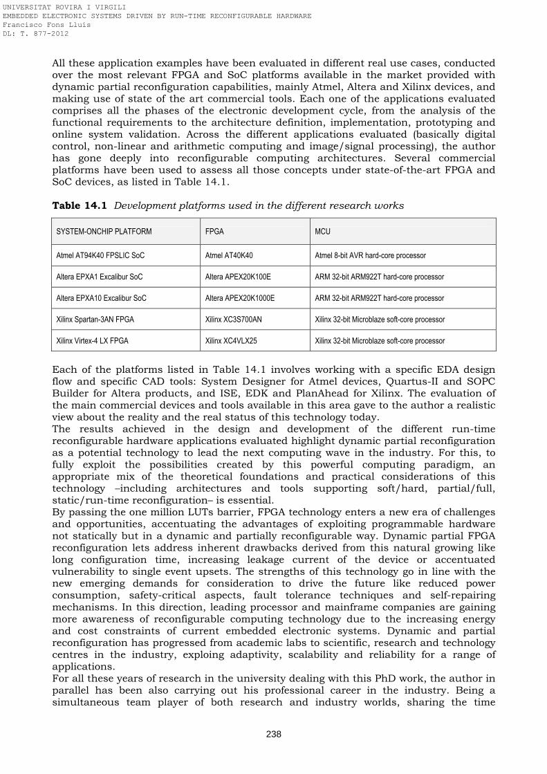
238
All these application examples have been evaluated in different real use cases, conducted over the most relevant FPGA and SoC platforms available in the market provided with dynamic partial reconfiguration capabilities, mainly Atmel, Altera and Xilinx devices, and making use of state of the art commercial tools. Each one of the applications evaluated comprises all the phases of the electronic development cycle, from the analysis of the functional requirements to the architecture definition, implementation, prototyping and online system validation. Across the different applications evaluated (basically digital control, non-linear and arithmetic computing and image/signal processing), the author has gone deeply into reconfigurable computing architectures. Several commercial platforms have been used to assess all those concepts under state-of-the-art FPGA and SoC devices, as listed in Table 14.1. Table 14.1 Development platforms used in the different research works
SYSTEM-ONCHIP PLATFORM FPGA MCU
Atmel AT94K40 FPSLIC SoC Atmel AT40K40 Atmel 8-bit AVR hard-core processor
Altera EPXA1 Excalibur SoC Altera APEX20K100E ARM 32-bit ARM922T hard-core processor
Altera EPXA10 Excalibur SoC Altera APEX20K1000E ARM 32-bit ARM922T hard-core processor
Xilinx Spartan-3AN FPGA Xilinx XC3S700AN Xilinx 32-bit Microblaze soft-core processor
Xilinx Virtex-4 LX FPGA Xilinx XC4VLX25 Xilinx 32-bit Microblaze soft-core processor
Each of the platforms listed in Table 14.1 involves working with a specific EDA design flow and specific CAD tools: System Designer for Atmel devices, Quartus-II and SOPC Builder for Altera products, and ISE, EDK and PlanAhead for Xilinx. The evaluation of the main commercial devices and tools available in this area gave to the author a realistic view about the reality and the real status of this technology today. The results achieved in the design and development of the different run-time reconfigurable hardware applications evaluated highlight dynamic partial reconfiguration as a potential technology to lead the next computing wave in the industry. For this, to fully exploit the possibilities created by this powerful computing paradigm, an appropriate mix of the theoretical foundations and practical considerations of this technology –including architectures and tools supporting soft/hard, partial/full, static/run-time reconfiguration– is essential. By passing the one million LUTs barrier, FPGA technology enters a new era of challenges and opportunities, accentuating the advantages of exploiting programmable hardware not statically but in a dynamic and partially reconfigurable way. Dynamic partial FPGA reconfiguration lets address inherent drawbacks derived from this natural growing like long configuration time, increasing leakage current of the device or accentuated vulnerability to single event upsets. The strengths of this technology go in line with the new emerging demands for consideration to drive the future like reduced power consumption, safety-critical aspects, fault tolerance techniques and self-repairing mechanisms. In this direction, leading processor and mainframe companies are gaining more awareness of reconfigurable computing technology due to the increasing energy and cost constraints of current embedded electronic systems. Dynamic and partial reconfiguration has progressed from academic labs to scientific, research and technology centres in the industry, exploing adaptivity, scalability and reliability for a range of applications. For all these years of research in the university dealing with this PhD work, the author in parallel has been also carrying out his professional career in the industry. Being a simultaneous team player of both research and industry worlds, sharing the time
UNIVERSITAT ROVIRA I VIRGILI EMBEDDED ELECTRONIC SYSTEMS DRIVEN BY RUN-TIME RECONFIGURABLE HARDWARE Francisco Fons Lluís DL: T. 877-2012
239
between two different and high demanding disciplines –PhD candidate in the Department of Electronic, Electrical and Automatic Control Engineering at the University Rovira i Virgili, and a full position as embedded electronic engineer in the industry–, has been a hard challenge not easy to carry ahead. However, with this dual view of the embedded electronic design world the author could gain experience and understanding on how new technologies are introduced in the industry. Under this perspective, the author believes that the level of maturity reached nowadays by the run-time reconfigurable hardware technology is good enough to be exploited –already in a professional way– in embedded applications of the real life. Through this PhD dissertation, the author uncovers the state of health of run-time reconfigurable hardware technology. At present, many potential killer apps, research projects and works disseminated in books, journals and conferences highlight the strengths of run-time reconfigurable hardware. Many researchers believe dynamically reconfigurable architectures are called to become platforms of choice for many applications in the not-to-distant future. One thing is true: the interest shown today by the scientific community for this technology is much higher than the interest shown some years ago, when the author started this research. Therefore, the advances done in this field are encouraging. However, in the modest opinion of the author, it is pending yet that the industry makes public more success stories in the professional use of this technology to definitively give a strong push of confidence on it.
14.2 Research projects
During all these years of work, the author, as an active member of the Development of Embedded Systems (DES) research group, has combined his research work with the participation in several European and Spanish funded research projects aligned with the interests of the PhD topic, where the DES research group has taken responsibility for tasks, work packages or other project deliverables. The author’s work falls within the scope of all these projects, as noted in the brief description of each of these projects that follows next. The list of projects is enumerated below in Table 1. Besides, the dissemination of results through books and journals, and the participation in International and National conferences have been regular and consolidated activities conducted for all this period. Table 14.2 European and Spanish research projects framework of this PhD dissertation
ACRONYM FULL PROJECT NAME SCOPE REFERENCE
TRUST-eS
Technology Responses to Ubiquitous Security Threads for e-Security
European project
FIT-070000-2003-930 and FIT-360000-2005-13 (MCyT, PROFIT, MEDEA+ A-306)
DELFIN
Development of a Fingerprint Co-processing System
Spanish project
SEG-2004-05592 (Plan Nacional de Investigación y Desarrollo, MCyT)
PIBES
Perfeccionamiento de la Identificación Biométrica y Evaluación de su Seguridad
Spanish project TEC2006-12365-C02-02 (MCyT)
14.2.1 TRUST-eS
During the past decade, Europe has led the development of smart-cards into complex media able to store, compute and securely manage multiple applications. However, there is a need to overcome technological limitations currently encountered in card-based transaction platforms to provide reliable and cost-effective solutions for e-security and e-government applications. In fact, cards employing conventional identity verification –passwords and PINs– are easily compromised while used in conjunction with biometrics offers one of the most reliable methods of determining individuals’ identities.
UNIVERSITAT ROVIRA I VIRGILI EMBEDDED ELECTRONIC SYSTEMS DRIVEN BY RUN-TIME RECONFIGURABLE HARDWARE Francisco Fons Lluís DL: T. 877-2012
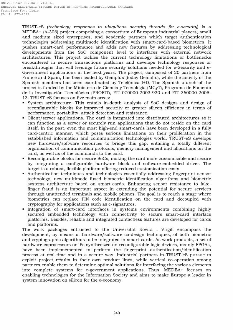
240
TRUST-eS (technology responses to ubiquitous security threads for e-security) is a MEDEA+ (A-306) project comprising a consortium of European industrial players, small and medium sized enterprises, and academic partners which target authentication technologies addressing multimode identification with smart-card-based biometrics. It pushes smart-card performance and adds new features by addressing technological developments from the SoC component level to interfaces with external network architectures. This project tackles the current technology limitations or bottlenecks encountered in secure transactions platforms and develops technology responses or breakthroughs that will leverage future security solutions needed for e-Security and e-Government applications in the next years. The project, composed of 20 partners from France and Spain, has been leaded by Gemplus (today Gemalto), while the activity of the Spanish members has been coordinated by Telefónica I+D. The Spanish branch of the project is funded by the Ministerio de Ciencia y Tecnología (MCyT), Programa de Fomento de la Investigación Tecnológica (PROFIT), FIT-070000-2003-930 and FIT-360000-2005-13. TRUST-eS focuses on five main areas: System architecture. This entails in-depth analysis of SoC designs and design of
reconfigurable blocks for improved security or greater silicon efficiency in terms of performance, portability, attack detection and resistance.
Client/server applications. The card is integrated into distributed architectures so it can function as a server or securely run applications that do not reside on the card itself. In the past, even the most high-end smart-cards have been developed in a fully card-centric manner, which poses serious limitations on their proliferation in the established information and communication technologies world. TRUST-eS develops new hardware/software resources to bridge this gap, entailing a totally different organisation of communication protocols, memory management and allocations on the card, as well as of the commands to the card.
Reconfigurable blocks for secure SoCs, making the card more customisable and secure by integrating a configurable hardware block and software-embedded driver. The target is a robust, flexible platform offering reduced customisation costs.
Authentication techniques and technologies essentially addressing fingerprint sensor technology, new multimode fused biometric identification algorithms and biometric systems architecture based on smart-cards. Enhancing sensor resistance to fake-finger fraud is an important aspect in extending the potential for secure services through unattended terminals and mobile phones. The goal is to reach a stage where biometrics can replace PIN code identification on the card and decoupled with cryptography for applications such as e-signatures.
Integration of smart-card interfaces in systems environments combining highly secured embedded technology with connectivity to secure smart-card interface platforms. Besides, reliable and integrated contactless features are developed for cards and platforms.
The work packages entrusted to the Universitat Rovira i Virgili encompass the development, by means of hardware/software co-design techniques, of both biometric and cryptographic algorithms to be integrated in smart-cards. As work products, a set of hardware coprocessors or IPs synthesized on reconfigurable logic devices, mainly FPGAs, have been implememented to perform the fingerprint authentication/identification process at real-time and in a secure way. Industrial partners in TRUST-eS pursue to exploit project results in their own product lines, while vertical co-operation among partners enable them to determine optimal solutions for interfacing the various elements into complete systems for e-government applications. Thus, MEDEA+ focuses on enabling technologies for the Information Society and aims to make Europe a leader in system innovation on silicon for the e-economy.
UNIVERSITAT ROVIRA I VIRGILI EMBEDDED ELECTRONIC SYSTEMS DRIVEN BY RUN-TIME RECONFIGURABLE HARDWARE Francisco Fons Lluís DL: T. 877-2012
241
14.2.2 DELFIN
DELFIN (development of a fingerprint co-processing system) is a Spanish project funded by the Plan Nacional de Investigación y Desarrollo from the Ministerio de Ciencia y Tecnología (McyT) under grant SEG-2004-05592, jointly developed by the Universitat Rovira i Virgili and the Universitat Politècnica de Catalunya. The goal of the project is the development of a low-power low-cost SoC platform so-called FICOS (FIngerprint COprocessing System) composed of an embedded processor with its corresponding data and program memories, and specific co-processors supporting the execution of the primitive operations of any access control system based on fingerprint biometrics, namely enrolment and matching. FICOS is connected to the external world through two interfaces: on the one hand, the fingerprint image is assumed to be stored in an external memory-like circuit (graphical interface); on the other hand, it receives commands and data from some external host processor (application interface). The definition of the corresponding communication protocols is part of the project. Internally FICOS includes a segmented flash memory able to store the features extracted from some reduced number of fingerprints. In some applications one or several of the flash memory segments are used for storing another type of confidential data, for example a private key used in some authentication protocol. The program executed by the embedded processor (firmware) depends on the particular application so that it is stored in another field-programmable non-volatile memory. A first prototype is built with an FPGA-based fast-prototyping board. A subsequent task is the evaluation of several lower cost solutions, among others: integration of the complete system within some type of commercial embedded array including the firmware and the flash memory, use of a low-cost sweep sensor and internal image reconstruction, and use of a dynamically programmable component, e.g. a SoC device, provided with dynamic partial reconfiguration capability. Furthermore, in order to evaluate the processor performance, a generic application is developed.
14.2.3 PIBES
Recent improvements in electronics and computer science have led to the consolidation of emerging technologies like biometrics. However, some initiatives for using biometrics in real applications have shown open issues that must be solved to enable its deployment and integration at large scale in everyday systems. PIBES (perfeccionamiento de la identificación biométrica y evaluación de su seguridad) is a Spanish project funded by the MCyT and split in two subprojects entitled “PIBES: Algorithmos Biométricos y Metodología de Evaluación” (TEC2006-12365-C02-01), coordinated by the University Carlos III, and “PIBES: Desarrollo de Coprocesadores Biométricos en Hardware Autoreconfigurable” (TEC2006-12365-C02-02), carried out by the Universitat Politècnica de Catalunya in conjunction with the Universitat Rovira i Virgili. PIBES approach tries to contribute to the improvement and validation of biometric systems in four major research lines: Solving some punctual problems currently unsolved in some biometric techniques, in
order to improve their performance and/or usability. Progress in developing multimodal biometric systems and increasing the verification
rates. Building biometric ID devices (biometric ID tokens) at lower cost and with higher
performance. Developing the design methodology and tools for the evaluation of the security of
biometric systems. The PIBES project pursues to improve the state-of-the-art of biometrics in some ways, providing interesting contributions to the scientific community in terms of new algorithms aimed at reducing the recognition error rates, making progresses in multi-modal biometrics as well as match-on-token, extract-on-token or even sensor-on-token
UNIVERSITAT ROVIRA I VIRGILI EMBEDDED ELECTRONIC SYSTEMS DRIVEN BY RUN-TIME RECONFIGURABLE HARDWARE Francisco Fons Lluís DL: T. 877-2012
242
devices, and delivering new guidelines and leassons learned focused on evaluation methodologies oriented to biometrics. From a social point of view, the project’s profits aims to bring biometrics identification closer to the citizens, so that they get familiar with this technology and have a bigger confidence in its techniques. Focused on the work conducted by UPC-URV group, at present, the implementation of biometric identification systems is usually based on high-performance and expensive general-purpose microprocessors or DSPs. The complex extraction and matching algorithms are normally designed or adapted to be executed with acceptable latencies over these kinds of platforms. However, these systems lack the presence of coprocessors specially designed for the execution of the compute intensive operations typically needed by the biometric algorithms. The UPC-URV group is focused in making interesting contributions in the development of embedded systems and hardware coprocessors designed for analyzing and processing extraction and matching biometric characteristics, devoted for developing low cost biometric recognition devices with extraction on token (EoT) and matching on token (MoT) capabilities. The system architecture proposed is based on a low-cost FPGA composed of a software host processor and several dedicated hardware coprocessors used for the resolution of the most time-critical tasks. This system architecture has proved to be competitive in terms of cost and very efficient in solving fingerprint algorithms and it is expected that similar hardware solutions can be applied to other biometric techniques, obtaining the advantages offered by this architecture. In fact, this possibility opens a novel research area, to be dealt in this project, based on developing specific tokens (single-mode) for different biometrics (voice, hand geometry, iris, etc) that can be integrated in low cost devices with high computational capabilities. Additionally, FPGAs are suited for applying dynamic self-reconfiguration techniques, which allow increasing the functional density of the programmable device in use. This characteristic, not used up to that moment in the development of biometric systems, enables the dynamic reconfiguration of a section of the FPGA, which works as a dynamic coprocessor able to map different functions in real-time, while the rest of the device maintains its static behaviour configured as an embedded microprocessor that controls the reconfiguration process and executes the non-time-critical tasks. The most important result of this approach is the significant reduction of the total area occupied by the system if compared with the area that would be obtained implementing the same system over a static and non-reconfigurable device. Dynamic self-reconfiguration is not only suitable for designing single-mode biometric tokens, but also for developing multimodal tokens (with two o more biometrics characteristics), a research line that is considered as one of the objectives of this project.
14.3 Future work
As future work, the author pursues to contribute to this research field in finding new opportunities for the deployment of run-time reconfigurable hardware technology in the industry – in the way of projects, applications or commercial products. The author belives that one effective way to consolidate the acceptance of this technology is to disseminate its potential through success stories in the industry/market. Exciting times lie ahead in the computing field and there will be plenty of computational problems and challenges to face where reconfigurable computing technology can help to solve them.
UNIVERSITAT ROVIRA I VIRGILI EMBEDDED ELECTRONIC SYSTEMS DRIVEN BY RUN-TIME RECONFIGURABLE HARDWARE Francisco Fons Lluís DL: T. 877-2012