DSPmagazine - AMiner
84
R INSIDE FPGA-Based MPEG-4 Codec Implementing Matrix Inversions in Fixed-Point Hardware Designing with the Virtex-4 XtremeDSP Slice The Design and Implementation of a GPS Receiver Channel INSIDE FPGA-Based MPEG-4 Codec Implementing Matrix Inversions in Fixed-Point Hardware Designing with the Virtex-4 XtremeDSP Slice The Design and Implementation of a GPS Receiver Channel Issue 1 October 2005 Simplifying DSP System Designs Simplifying DSP System Designs DSP magazine DSP magazine SOLUTIONS FOR HIGH-PERFORMANCE SIGNAL PROCESSING DESIGNS
-
Upload
khangminh22 -
Category
Documents
-
view
1 -
download
0
Transcript of DSPmagazine - AMiner

R
INSIDE
FPGA-Based MPEG-4 Codec
Implementing Matrix Inversions in Fixed-Point Hardware
Designing with the Virtex-4 XtremeDSP Slice
The Design andImplementation of a GPS Receiver Channel
INSIDE
FPGA-Based MPEG-4 Codec
Implementing Matrix Inversions in Fixed-Point Hardware
Designing with the Virtex-4 XtremeDSP Slice
The Design andImplementation of a GPS Receiver Channel
Issue 1October 2005
Simplifying DSPSystem DesignsSimplifying DSPSystem Designs
DSPmagazineDSPmagazineS O L U T I O N S F O R H I G H - P E R F O R M A N C E S I G N A L P R O C E S S I N G D E S I G N S

Enabling success from the center of technology™
1 800 332 8638
www.em.avnet.com
© Avnet, Inc. 2005. All rights reserved. AVNET is a registered trademark of Avnet, Inc.
Avnet Electronics Marketing has collaborated with National
Semiconductor® and Xilinx® to create a design guide that
matches National Semiconductor’s broad portfolio of power
solutions to the latest releases of FPGAs from Xilinx.
Featuring parametric tables, sample designs and step-by-step
directions, this guide is your fast, accurate source for choosing the
best National Semiconductor Power Supply Solution for your design.
It also provides an overview of the available design tools, including
application notes, development software and evaluation kits.
Go to em.avnet.com/powermgtguide
to request your copy today.
Support Across The Board.™
Power Management Solutions for FPGAs
National Devices supported:
• Voltage Regulators
• Voltage Supervisors
• Voltage References
Xilinx Devices supported:
• Virtex™
• Virtex-E
• Virtex-II
• Virtex-II Pro
• Virtex-4FX, 4LX, 4SX
• Spartan™-II
• Spartan™-IIE
• Spartan-3, 3E, 3L

Welcome ...........................................................................................................4
VIEWPOINT
Setting Industry Direction for High-Performance DSP ...................................................5
MULTIMEDIA, VIDEO, and IMAGING
FPGA-Based MPEG-4 Codec.................................................................................8
Rapid Development of Video/Imaging Systems .......................................................10
Encoding High-Resolution Ogg/Theora Video with Reconfigurable FPGAs ...................13
Implementing DSP Algorithms Using Spartan-3 FPGAs ..............................................16
Using FPGAs in Wireless Base Station Designs .......................................................20
Accelerated System Performance with APU-Enhanced Processing ................................24
Alpha Blending Two Data Streams Using a DSP48 DDR Technique.............................28
DEFENSE SYSTEMS
Implementing Matrix Inversions in Fixed-Point Hardware............................................32
Integrating MATLAB Algorithms into FPGA Designs...................................................37
Software-Defined Radio: The New Architectural Paradigm.........................................40
Virtex-4 FPGAs for Software Defined Radio.............................................................44
DIGITAL COMMUNICATION
Real-Time Analysis of DSP Designs ........................................................................46
The Design and Implementation of a GPS Receiver Channel......................................50
GENERAL PURPOSE AND IMPLEMENTATION
Designing Control Circuits for High-Performance DSP Systems ....................................55
Signal Processing Capability with the NuHorizons Spartan-3.....................................59
Designing with the Virtex-4 XtremeDSP Slice............................................................62
Synthesis Tool Strategies......................................................................................66
CUSTOMER SUCCESS
A Weapon Detection System Built with Xilinx FPGAs ................................................68
EDUCATION
DSP Design Flow – Intermediate Level....................................................................72
PRODUCT BRIEFS
Virtex-4 SX 35 XtremeDSP Development Kit for Digital Communication Applications .......74
Virtex-II Pro XtremeDSP Development Kit for Digital Communication Applications ............76
Virtex-4 DSP Brochure .........................................................................................79
C O N T E N T S
D S P M A G A Z I N E I S S U E 1 , O C T O B E R 2 0 0 5
F
High-Performance DSP – Vision, Leadership, CommitmentFPGAs are increasingly being used for signal processing applications. They provide the necessaryperformance and flexibility to tackle many of today’s most challenging DSP applications, fromMIMO digital communication systems to H.264 encoding to a high-definition broadcast system.
Within such systems, FPGAs are ideally suited for high-performance signal-processing tasks traditionally serviced by an ASIC or ASSP. But you can also use FPGAs to create high-performanceDSP engines that boost the performance of your programmable DSP system by performing complementary co-processing functions.
This unique coupling of high performance and flexibility – through exploiting parallelism andhardware reconfiguration – places Xilinx in an ideal position to set the industry direction in thehigh-performance segment of the DSP market.
Our DSP vision is built on five key pillars:
• Customer and market focus – we will create products that meet the needs of our customersand create products in those market segments that are the best fit for our FPGAs.
• Design methodology – as most DSP designers don’t speak VHDL or Verilog, we will continue to evolve software technologies to support languages that they do speak – like Simulink and MATLAB.
• Tailored system solutions – this includes algorithms, tools, services, and devices for focus markets.
• Ecosystem – partnerships/alliances with industry leaders like Texas Instruments, The MathWorks, and Xilinx Global Alliance members to deliver total DSP solutions.
• Awareness – educating you on how to quickly access FPGAs for signal processing regardless of your background skill set.
This month we are also launching new DSP Roadmaps for the high-performance segment of theDSP market. These roadmaps cover many areas, including digital communications, multimediavideo and imaging, defense systems, design tools and methodologies, development platforms, andbase IP solutions. The roadmaps demonstrate our continued investment and commitment in solving your current and future signal-processing challenges.
Finally, we are proud to deliver to you the first edition of DSP Magazine. Packed with articlesdemonstrating how you can create optimized DSP designs using FPGAs, this magazine is one ofmany ways in which we will provide you the knowledge to finish your DSP designs faster. I wouldlike to dedicate this first Xilinx DSP Magazine to you, the customer.
Xilinx, Inc.2100 Logic DriveSan Jose, CA 95124-3400Phone: 408-559-7778FAX: 408-879-4780
© 2005 Xilinx, Inc. All rights reserved. XILINX, the Xilinx Logo, and otherdesignated brands included here-in are trademarks of Xilinx, Inc. PowerPC is a trademark ofIBM, Inc. All other trademarks are the property of theirrespective owners.
The articles, information, and other materials included inthis issue are provided solely for the convenience of ourreaders. Xilinx makes no warranties, express, implied,statutory, or otherwise, and accepts no liability with respectto any such articles, information, or other materials or theiruse, and any use thereof is solely at the risk of the user.Any person or entity using such information in any wayreleases and waives any claim it might have against Xilinxfor any loss, damage, or expense caused thereby.
Omid Tahernia
Vice President and General ManagerXilinx DSP Division
EDITOR IN CHIEF Carlis [email protected]
EXECUTIVE EDITOR Forrest [email protected]
MANAGING EDITOR Charmaine Cooper Hussain
ONLINE EDITOR Tom [email protected]
ART DIRECTOR Scott Blair
ADVERTISING SALES Dan Teie1-800-493-5551
DSPmagazineDSPmagazine

by Jack ElwardSenior Director, Program Management, DSP DivisionXilinx, [email protected]
Have you ever been on a long trip, in some-what unfamiliar territory, and in search ofyour next move? You would certainly wel-come a map that shows what the roadholds in store ahead. Not only is it inform-ative, it can also be reassuring. A good roadmap will contain enough details about yourintended travel path so that you can confi-dently charge forward or plan for back-upsand alternatives. Of course, sometimes youwill want to contact your travel advisor formore details.
Such is the intent of the DSP Roadmapfrom Xilinx. In publishing the most com-prehensive, detailed set of IP, product, andtools plans ever attempted, we intend toshine a floodlight on our next few years oftechnical releases.
DSP Strategic PillarsThe Xilinx® DSP initiative is based on fivestrategic pillars:
• Market focus
• Design methodology
• Tailored solutions
• Ecosystem
• Awareness
These pillars are manifested in the DSPRoadmap in the following important ways:
For market focus, we listen to cus-tomers and their needs and select high-growth markets where we can add themost value through our products and serv-ices. Xilinx target segments include digitalcommunications (both wired and wire-less), aeronautics and defense, and MVI(multimedia, video, and imaging). OtherDSP markets (such as test and measure-
ment, industrial, and telemetrics) are wellserved by our current products and theirfuture roadmaps.
Design methodology refers to a growingawareness that traditional users of FPGAs(using VHDL and Verilog) represent onlyabout 10% of the DSP design community.The vast majority of these designers are:
• More familiar with software designtools such as C, C++, and MATLAB,
Setting Industry Direction for High-Performance DSPSetting Industry Direction for High-Performance DSP
October 2005 DSP magazine 5
Xilinx launches new market-focused DSP Roadmaps.Xilinx launches new market-focused DSP Roadmaps.
Applications Expertise
DSP Services
Design/Verification Tools
Hardware Platforms
DSP Algorithms (IP)
ICs
• New DSP Division, Partnerships, Specialists
• Design Services, Education and Support
• System Generator for DSP, Third-Party EDA
• Development Platforms, Starter Kits
• RACH Rx, Searcher, MPEG4
• Optimized Next Generation Co-Processing Interfaces
Complete DSP Design Solutions
Figure 1 – Solutions spectum

and a methodology that assumes arobust library of function calls andhardware layer abstraction
• Schooled or experienced in using DSPproducts from TI, ADI, and Freescale
• In search of higher bandwidth and per-formance, which can be best deliveredthrough the parallelism of FPGAs
• Concerned with system-level integra-tion, software compatibility and reuse,and rapid prototyping
The tailored solutions strategic pillar is anatural evolution of our traditional build-ing blocks (such as FFT, FIR filters, andother “base blocks”) for general DSP appli-cations. There are three clear tines in thisfork: IP, tools, and FPGA devices.
In addressing the ecosystem, Xilinx isacknowledging a successful strategy alreadyemployed throughout our history. We start-ed off as one of the first fabless semiconduc-tor companies and forged strategic allianceswith companies like IBM and TI. Now, witha broad set of IP and tools developed by andoffered from third-party vendors, wedemonstrate how important it is to gobeyond our internal development resourcesto provide increasingly complete solutions.
Finally, awareness is crucial in affectingthe sea change that we desire in positioningXilinx as a major supplier of DSP solutions.We are clearly positioned and recognized asthe world leader in programmable logic,but traditional customer surveys of “DSPsupplier awareness” show that we have anuphill climb in the field of entrenched DSPproviders such as TI. The roadmaps are aprimary vehicle in communicating theexpansion of expertise and product offer-ings, which the recently formed DSP divi-sion is capable of delivering.
The DSP Roadmaps cover a broadrange of products and services. Figure 1shows the solution spectrum, ranging fromDSP devices to design tools and designservices. Tools are inclusive of IP, libraries,boards, and kits.
IP and SolutionsTraditional offerings for DSP designershave been horizontal in nature and apply to
processor and DSP48 blocks. These coresinclude a floating point co-processor con-nected to the PowerPC through a dedicat-ed hardware port, and several coresembracing the versatility and inherent per-formance of the DSP48 slices in their cas-caded configuration.
The IP offerings are tailored to meet theneeds of specific vertical markets.Therefore, we have created roadmaps toaddress the following areas: Digital
market segments. Elements such as FFTs,FIR filters/compilers, encryption, and lin-ear algebra are good examples. The DSPRoadmaps continue to offer enhancementsto the functionality and performance,along with forward migration into newgenerations of FPGA families.
We are also introducing new buildingblocks to work in conjunction with com-plex, hard IP embedded into Xilinx FPGAfamilies, such as the PowerPC™ 405
6 DSP magazine October 2005
Figure 2 – Digital Communications DSP Roadmap
Figure 3 – Multimedia, Video, and Imaging Systems DSP Roadmap

October 2005 DSP magazine 7
Communication Systems; Multimedia,Video, and Imaging (MVI) Systems; andDefense Systems (represented in Figures2, 3, and 4, respectively). Each of theseroadmaps contains specialized compo-nents or solution platforms. This repre-sents the collective expertise of developers,application engineers, and field technicalexperts in conjunction with invaluableinput from customers.
In addition to developing building-block IP, Xilinx is moving toward sets ofproducts intended to provide proof of con-cept, and in some cases, reference qualitydesigns that can be adopted directly intocustomer solutions. Examples in the digitalcommunications arena are in the 3GPPand W-CDMA standards in radio-shelfand base-band implementations. New areasof rapidly growing interest are the WiMAX
standards and Picocell architectures.Similar solutions are included in each ofthe other market-focused roadmaps.
ToolsThe Tools and Methodologies Roadmapshown in Figure 5 illustrates our desire toaddress the designer community in threemajor tiers: traditional Xilinx hardware(FPGA) designers, DSP developmentengineers, and system designers. Thestrategy is built on the Xilinx ISE™ soft-ware tools suite, but incorporates SystemGenerator for DSP, our embedded devel-opment tool suites, and other third-partyofferings. If you haven’t reviewed this arearecently, you will be quite surprised to seethe advances in capability and perform-ance that have been introduced and arecoming over the next few releases.
DevicesThe Spartan™ and Virtex™ FPGA fam-ilies have continued to evolve and includespecific functions that optimize perform-ance and power for specific applicationareas. The multipliers, DSP48, andembedded processors are examples ofcontent directly aimed at the DSP field.The Virtex-4 generation identified sub-families that allow focused concentrationsof features for cost-optimized delivery. Inthe roadmap for future devices, you willcontinue to see this focus played out withadditional specialized circuits and build-ing blocks committed to silicon.
ConclusionThe DSP Roadmaps are not intended tobe a one-way communication. In pre-senting our vision of the future, weexpect to initiate and share in a dialogwith others. We intend to engender dis-cussion and commentary. This is ahealthy process of discovery that ulti-mately leads to better products fromXilinx that help you develop and deliverbetter products to your customers. Welook forward to this dialog and learningbetween Xilinx and the DSP world.
For more information about our newproducts and DSP Roadmaps, visit DSPCentral at www.xilinx.com/dsp.
Figure 4 – Defense Systems DSP Roadmap
Figure 5 – DSP Tools and Methodolgies Roadmap
by Paul SchumacherSenior Staff Research Engineer Xilinx, [email protected]
Wilson ChungSenior Staff Video and Imaging EngineerXilinx, [email protected]
Have you ever wanted to include state-of-the-art video compression in your FPGAdesign but found it too complex an under-taking? You no longer need to be a videoexpert to include video compression in yoursystem. Newly released MPEG-4encoder/decoder cores from Xilinx can helpsolve your video compression needs.
Video and multimedia systems arebecoming increasingly complex, and theavailability of low-cost, reliable IP cores foryour system is crucial to getting your productto market. In particular, video compressionalgorithms and standards have becomeextremely complicated circuits that can takea long time to design and are quite often bot-tlenecks in getting a system tested andshipped. These MPEG-4 simple profileencoder/decoder cores may just do the trickfor your next multimedia system.
ApplicationsMPEG-4 Part 2 is a recent internationalvideo coding standard in a series of suchstandards: H.261, MPEG-1, MPEG-2,and H.263. It was approved by ISO/IEC asInternational Standard 14 496-2 (MPEG-4Part 2) in December 1999. The MPEG-4Part 2 video codec provides an excellentbasis for a number of multimedia applica-tions. The standard provides a set of pro-files and levels to allow for a plethora ofdifferent application requirements, such asframe size and use of error-resilience tools.Examples of these applications include
broadcasting, video editing, teleconferenc-ing, security/surveillance, and consumerelectronics applications.
The video coding algorithm used inMPEG-4 Part 2 is an evolution from previouscoding standards. The frame data is dividedinto 16 x 16 macroblocks containing six 8 x 8blocks for YCbCr 4:2:0 formatted data.Motion estimation with half-pixel resolutionis used to efficiently code predicted blocksfrom the previous frame, while the discretecosine transform (DCT) provides the residualprocessing to create a more detailed view ofthe current frame. Simple profile provides 12bits of resolution for DCT coefficients with 8bits per sample for the sampled and recon-structed frame data. Coding efficiency of theMPEG-4 simple profile is better than the pre-vious generation in MPEG-2 across a rangeof coding bit rates.
A typical multimedia system can useMPEG-4 as the video compression compo-nent within a larger system. An example ofthis is an end-to-end video conferencing sys-
tem delivering compressed bitstreams betweentwo or more participants. Designations forthese sources can modify system requirements,where a key speaker or presenter for a confer-ence may require higher resolution video aswell as audio. This type of system can beexpanded to video surveillance and securityapplications, where a display station user maydecide to keep a mosaic of all video cameras orfocus in on a single camera view for detailedreal-time analysis. These applications requirethat the stream selection is performed at thereceiver and is capable of handling real-timeviewing specifications.
An FPGA provides an excellent program-mable concurrent processing platform thatallows for support of varying system require-ments while meeting the needs of systemthroughput. The Xilinx® MPEG-4 decodercore can be built with a scalable, multi-streaminterface customized for your application andsystem requirements, while both the MPEG-4encoder and decoder are also capable of servic-ing a user-specified maximum frame size.
FPGA-Based MPEG-4 Codec
8 DSP magazine October 2005
Using FPGAs to implement complex video codecs goes beyond ASIC prototyping.
blockFIFO (2)
blockFIFO (2)bl
ock
FIF
O (
2)
scalarFIFObl
ock
FIF
O (
3)
bloc
kF
IFO
(3)
bloc
kF
IFO
(2)
TextureUpdate
TextureCoding
VariableLengthCoding
BitstreamPacketization
MotionCompensation
Shared Mem
Shared Mem
MemoryController
CopyController
ExternalSRAM
Burst 64Register File
SoftwareOrchestrator(Rate Control
and Parameters)
MotionEstimation
InputController
MPEG-4 SP Encoder Core
Burst 64
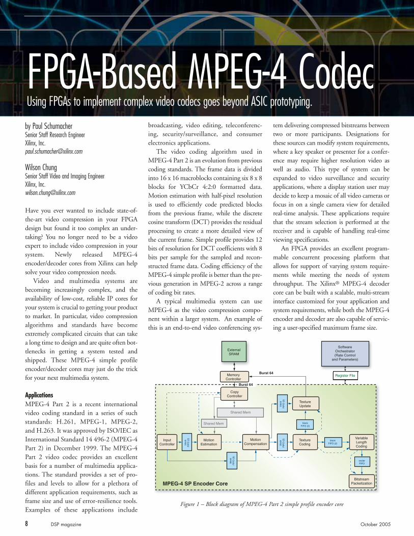
Figure 1 – Block diagram of MPEG-4 Part 2 simple profile encoder core
ArchitectureFigures 1 and 2 illustrate the block diagramsfor the MPEG-4 simple profile encoder anddecoder cores, respectively. Hardware-based,pipelined architectures were used for theseimplementations, with a host interface pro-vided on the encoder for software-controlledrate control. With an included memory con-troller, the raw, captured sequence for theencoder and the reconstructed frames for thedecoder are stored in an off-chip memory forfast, low-latency access to the pixel data. Asimple FIFO interface is provided for com-municating the compressed bitstreams, withthe decoder custom-built for a user-specifiednumber of bitstreams. A system interface isalso included to allow for maximum control-lability and observability.
To create scalable multi-stream designs thatcan meet the needs of different applications,the package provided with the core contains anumber of user-specified, compile-timeparameters that allow you to customize theencoder and decoder. To create a resource-effi-cient design, you can also set the maximumsupported frame width and height. The com-piled design would then include enough mem-ory and registers to support any framedimensions less than or equal to these twoparameters. Other parameters give you com-plete control over the scalability of the finaldesign and craft a system built exclusively foryour application.
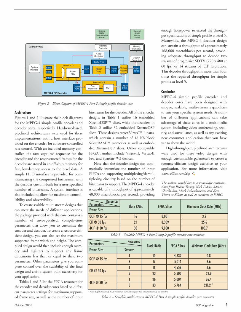
Tables 1 and 2 list the FPGA resources forthe encoder and decoder cores based on differ-ent parameter settings for maximum support-ed frame size, as well as the number of input
enough horsepower to exceed the through-put specifications of simple profile at level 5.Meanwhile, the MPEG-4 decoder designcan sustain a throughput of approximately168,000 macroblocks per second, provid-ing adequate throughput to decode twostreams of progressive SDTV (720 x 480 at60 fps) or 14 streams of CIF resolution.This decoder throughput is more than fourtimes the required throughput for simpleprofile at level 5.
ConclusionMPEG-4 simple profile encoder anddecoder cores have been designed withunique, scalable, multi-stream capabilitiesto suit your specific system needs. A num-ber of different applications can takeadvantage of these cores in a multimediasystem, including video conferencing, secu-rity, and surveillance, as well as any excitingnew consumer application that you haveyet to show the world.
High-throughput, pipelined architectureswere used for these video designs withenough customizable parameters to create aresource-efficient design exclusive to yourapplication. For more information, visitwww.xilinx.com/dsp.
The authors would like to acknowledge contribu-tions from Robert Turney, Nick Fedele, AdrianChirila-Rus, Mark Paluszkiewicz, and KeesVissers at Xilinx, as well as members at IMEC.
bitstreams for the decoder. All of the encoderdesigns in Table 1 utilize 16 embeddedXtremeDSP™ slices, while the decoders inTable 2 utilize 32 embedded XtremeDSPslices. These designs target Virtex™-4 parts,which contain a number of 18 Kb blockSelectRAM™ memories as well as embed-ded XtremeDSP slices. Other compatibleFPGA families include Virtex-II, Virtex-IIPro, and Spartan™-3 devices.
Note that the decoder design can auto-matically instantiate the number of inputFIFOs and supporting multiplexing/demul-tiplexing circuitry based on the number ofbitstreams to support. The MPEG-4 encoderis capable of a throughput of approximately48,000 macroblocks per second, providing
October 2005 DSP magazine 9
SystemInterface
FIFO
FIFO
FIFO
Parser/VLD
ParserFSM
Pre-Processor
Object FIFO
IDCT
MotionComp.
FIFO
Buffer YUV
ObjectFIFO
ObjectFIFO
ObjectFIFO
TextureUpdate
DisplayController
MemoryController
MemoryController
Texture/IDCT
CopyController
ExternalSRAM
ReconstructedFrame
ExternalSRAMDisplayFrame
MPEG-4 SP Decoder
Xilinx FPGA
Frame SizeBlock RAMs FPGA Slices Minimum Clock Rate (MHz)
QCIF @ 15 fps 16 8,051 3.2CIF @ 30 fps 21 8,309 25.64CIF @ 30 fps 30 9,000 100.7
ParametersResources
Frame Size StreamsBlock RAMs FPGA Slices Minimum Clock Rate (MHz)
QCIF @ 15 fps1 10 4,332 0.88 17 5,014 6.6
CIF @ 30 fps1 16 4,558 6.68 23 5,305 52.8
4CIF @ 30 fps1 26 5,004 26.48 33 5,764 211.2 *
Parameters Resources
Figure 2 – Block diagram of MPEG-4 Part 2 simple profile decoder core
Table 1 – Scalable MPEG-4 Part 2 simple profile encoder core resources
Table 2 – Scalable, multi-stream MPEG-4 Part 2 simple profile decoder core resources
* Note: Eight streams of 4CIF resolution currently require two instantiations of the decoders.

by Hong-Swee LimSenior Manager, DSP Product and Solutions MarketingXilinx, [email protected]
Advances in media encoding schemes areenabling a broad array of applications,including digital video recorders(DVRs), network surveillance cameras,medical imaging, digital broadcasting,and streaming set-top boxes. The prom-ise of streaming media presents a seriesof implementation challenges, especiallywhen processing complex compressionalgorithms such as MPEG-4 andMPEG-compressed video transcoding.Given the high computational horse-power required for encoding or decodingsuch complex algorithms, achievingoptimal balance of power, performance,and cost is a significant challenge forstreaming media devices.
By using FPGAs, you can differentiateyour standard-compliant systems fromyour competitor’s products and achievethe optimal balance for your application.With the MPEG-4 compression scheme,for example, it is possible to offload theIDCT (inverse discrete cosine transform)
portion of the algorithm from an MPEGprocessor to an FPGA to increase the pro-cessing bandwidth. IDCT (and DCT atthe encoder) can be implementedextremely efficiently using FPGAs, andoptimized IP cores are readily available toinclude in MPEG-based designs.
By integrating various IP cores togetherwith the IDCT core, you can develop alow-cost, single-chip solution that increas-es processing bandwidth and gives higherquality images than your competitor’sASSP-based solution.
To help you accelerate your systemdesign, Xilinx offers the Video Starter Kit(VSK) 4VSX35. The VSK is an all-digitalplatform for real-time video/image acqui-sition, processing, and display. It integratesthe power of hardware-accelerated process-ing as well as an embedded PowerPC™core for the transmission of high-resolu-tion digital video over lower bandwidths,or for processing network protocol stackand control functions.
Xilinx Video Starter Kit 4VSX35The Xilinx® VSK 4VSX35 allows you tojump-start your high-performance audio,video, and imaging processing designs. At
the heart of the VSK are two highly pro-grammable Xilinx FPGAs (XC2VP4 andXC4VSX35), video encoder, videodecoder, AC97 CODEC, and a wide rangeof video interfaces.
Figure 1 illustrates the VSK’s primarycomponents, peripherals, and available I/O.
The VSK comprises three major hard-ware components: a Xilinx ML402-SX35board; 752 x 480-pixel RGB progressivescan CMOS image-sensor camera with aframe rate as high as 60 frames per second(fps); and video I/O daughtercard(VIODC). The VIODC is connected tothe ML402-SX35 board through the XilinxGeneric Interface (XGI), while the CMOScamera is connected to the VIODCthrough the serial LVDS interface.
The video encoder is a high-speed,video digital-to-analog converter. It hasthree separate 10-bit-wide input portsthat accept data in high- or standard-defi-nition video formats. It also controls theinsertion of appropriate synchronizationsignals; external horizontal, vertical, andblanking signals; or EAV/SAV timingcodes for all standards.
The video decoder is a high-quality, sin-gle-chip, multi-format video decoder that
Rapid Development of Video/Imaging SystemsRapid Development of Video/Imaging Systems
10 DSP magazine October 2005
Build real-time video and imaging applications quickly and easily with the Xilinx Video Starter Kit.Build real-time video and imaging applications quickly and easily with the Xilinx Video Starter Kit.

automatically detects and converts PAL,NTSC, and SECAM standards in the formof composite, S-Video, and componentvideo into a digital ITU-R BT.656 format.The advanced and highly flexible digitaloutput interface enables performance videodecoding and conversion in line-lockedclock-based systems. This makes the VSKideally suited for a broad range of applica-tions with diverse video characteristics,including broadcast sources, security andsurveillance cameras, and professionalvideo systems. Figure 2 shows a block dia-gram of the Video Starter Kit.
With the video encoder, video decoder,DVI receiver, DVI transmitter, and camerasupporting a two-wire serial I2C-compati-ble interface, all of these devices can becontrolled through an I2C master corelocated either in the XC4VSX35 orXC2VP4 device.
The flexibility of the VSK architecturemakes it suitable as a development plat-form for a variety of multimedia, video,and imaging applications, which include:
• Medical imaging
• Home media gateways
• Multi-channel digital video recorders
• IP TV set-top boxes
• Video-on-demand servers
• Digital TV
• Digital camera and camcorders
• A/V broadcasts
• Network surveillance cameras
System Generator for DSP v8.1Converting image processing algorithms toFPGA implementations can be challeng-ing, as the algorithms may be proven insoftware but not directly linked to the actu-al implementation. Additionally, it can bedifficult to subjectively verify the imple-mentation.
Xilinx System Generator for DSP allowsfor high-level mathematical verificationand converts the heart of the algorithminto ready-to-use HDL, which bridges thegap from the algorithm developer to theFPGA engineer.
boundaries when determining implemen-tation trade-offs.
To accelerate video/imaging systemdevelopment, Xilinx has developed newSystem Generator blocks specifically forthe VSK, including:
• VIODC interface block
• Multi-port DDR memory controller block
• System-level blocks
With these pre-testedblocks, you can easily buildyour video/imaging systemby just dragging and drop-ping the blocks withinSystem Generator to con-struct your system, savingprecious time from codingthese essential interfacingblocks in HDL.
To be able to handle theenormous video data stream
Using System Generator and the VSKto develop and implement image-process-ing algorithms allows for a thoroughly ver-ified and easily executed design. Thehigh-level block diagram allows for easycommunication between team members,resulting in less time spent crossing skill
October 2005 DSP magazine 11
ComponentVideo
CompositeVideo
S-Video
HD-SDI
S-VideoInput
ComponentVideo
CompositeVideo
S-Video
HD-SDI
S-VideoOutput
Line Out/Headphone
Mic In/Line In
Serial
Camera
USBPeripherals
USB Host
RJ45
Video I/O Daughtercard
ML402
Video Decoder
Cable Equalization
DVI Receiver
Camera Interface
Video Encoder
Cable Driver
DVI Transmitter
AC97 Audio CODEC
RS232
16x32 Character
LCD
FLASH DDR SDRAM
USB Controller
Ethernet Interface
JTAG Header
Xilinx FPGAXC2VP4
Xilinx FPGAXC4VSX35
Figure 1 - Video Starter Kit 4VSX35
Figure 2 - Block diagram of Video Starter Kit 4VSX35

12 DSP magazine October 2005
from the VSK to the PC, another innova-tive high-speed hardware co-simulationthrough an Ethernet interface was intro-duced in System Generator for DSP 8.1.This interface allows high throughputwith low latency, which proved to beextremely useful when buildingvideo/imaging systems in the SystemGenerator environment.
Network Surveillance Camera ApplicationFPGAs have historically been found inhigh-end professional broadcast systemsand medical imaging equipment. TodayFPGAs are also finding their way intohigh-volume products such as digitalvideo recorders and network surveillancecameras because of their flexibility in han-dling a broad range of media formats suchas MPEG-2, MPEG-4, H.264, andWindows Media. Their extremely high-performance DSP horsepower also makesFPGAs suitable for other challengingvideo and audio tasks.
Typically, a network surveillance cam-era product comprises three parts: a cam-era to convert the real-world image into avideo stream; a video decoder for streamscompressed into H.264, MPEG-2, oranother format; and a video/image proces-
sor for de-interlacing, scaling, and noisereduction before packeting the digitizedvideo for transmission over the Internet.
FPGAs can have many areas of respon-sibility within surveillance cameras, asshown in Figure 3. Bridging betweenstandard chipsets as “glue logic” hasalways been a strong application ofFPGAs, but many more image-processingtasks (such as color-space conversion),IDE (Integrated Drive Electronics) inter-face, and support for network interfaces(such as IEEE 1394) are now also com-monly implemented in low-cost pro-grammable devices.
With high-performance DSP capabili-ty inside a network surveillance camera,you can digitize and encode the videostream to be sent over any computer net-work. You can use a standard Web brows-er to view live, full-motion video fromanywhere on a computer network, includ-ing over the Internet. Installation is sim-plified by using existing LAN wiring orwireless LAN. Features such as intelligentvideo, e-mail notification, FTP uploads,and local hard-disk storage provideenhanced differentiation and superiorcapability over analog systems.
The hard-processor core is an IBM
PowerPC 405 immersed in a XilinxVirtex™-II Pro™ FPGA, delivering 600DMIPS at 400 MHz runningMontaVista Linux or Wind RiverSystems’s VxWorks real-time operatingsystem (RTOS), as well as a network pro-tocol stack to implement these features.
Xilinx also offers the MicroBlaze™32-bit RISC processor core, delivering upto 138 DMIPS at 150 MHz and 166DMIPS at 180 MHz when used in theVirtex-II Pro and Virtex-4 devices,respectively.
Conclusion Bandwidth is precious; to make the mostof it, compression schemes have steadilyimproved – and new algorithms push theenvelope even further. As such, system-processing rates have increased over time,and real-time image processing is an idealway to meet these requirements whileremoving memory overhead.
At the same time, Moore’s Law hasresulted in low-cost programmable logicdevices, such as the new FPGAs, that pro-vide the same functionality and perform-ance previously found only in expensiveprofessional broadcast products.
FPGAs provide both professional andconsumer digital broadcast OEMs withreal-time image processing capabilitiesthat address the system requirements ofnew and emerging video applications.Compared to other technologies, FPGAsoffer an unrivalled flexibility that enablesyou to get your products to marketquickly. Remote field upgradeabilitymeans that systems can be shipped nowand features, upgrades, or design fixesadded later.
The VSK has been architected toreduce implementation risks, time tomarket, and development costs. By pro-viding hardware and MPEG-4 IP in apre-tested and integrated platform, youcan concentrate on implementing theapplication-specific video and imagingfunctionality that is most relevant to yourparticular product.
For more information, visit www.xilinx.com/products/design_resources/dsp_central/grouping/index.htm.
CMOSCamera
MIC
NTSC/PALDecoder
AudioProcessing IP
AC97CODEC
Flash SDRAM
Custom IP
EthernetPHY
VideoEncoder
Application
TCP/IP Stack
RTOS
Processor Core
MPEG-4CODEC IP Monitor
RJ45
Hard Disk
Video Starter Kit 4VSX35
Figure 3 - Network surveillance camera

by Andrey FilippovPresidentElphel, [email protected]
Much of the Spring 2003 issue of the XcellJournal in which my article aboutSpartan™-IIE-based Elphel Model 313cameras appeared (“How to Use FreeSoftware in FPGA Embedded Designs”)was dedicated to the Xilinx® Spartan-3FPGA. I immediately started to thinkabout using these devices in our new gen-eration of Elphel network cameras, but itwasn’t until last year that I was finally ableto start working with them.
One of the factors that slowed my com-pany’s adoption of this new technology wasthe fact that at first I could not find appro-priate software that could handle thedevices selected, as it is essential that ourend users can modify our products withoutexpensive software development tools.When I visited the Xilinx website inSummer 2004 and found that the currentversion of the free downloadableWebPACK™ software could handle theXC3S1000 – the largest device available ina small FT256 package – I knew it was theright time to switch to the Spartan-3 device.
Encoding High-Resolution Ogg/Theora Video with Reconfigurable FPGAs
Encoding High-Resolution Ogg/Theora Video with Reconfigurable FPGAs
October 2005 DSP magazine 13
Once the traditional application area of custom ASICs, modern FPGAs can now handle high-performance video encoding.Once the traditional application area of custom ASICs, modern FPGAs can now handle high-performance video encoding.

The Camera HardwareThe new Model 333 camera (Figure 1) uses the same Linux-optimized CPU(ETRAX100LX by Axis Communications)as the earlier Model 313, but withincreased system memory – 32 MB ofSDRAM and 16 MB of Flash. The secondmajor upgrade is the use of 32 MB of DDRSDRAM as a dedicated frame buffer thatworks in tandem with the FPGA, supple-menting its processing power with highcapacity and I/O bandwidth.
The Spartan-3 DDR I/O functionalitymade it possible to increase the memorybandwidth without increasing board size –the complete system still fits on a 1.5 x 3.5-inch four-layer board (see Figure 2). Theactual board area is even smaller, as the newone is designed to fit the sealed RJ45 con-nectors for outdoor applications.
For the camera circuit design, the goalsinclude combining high computational per-formance with small size (that also simpli-fies preserving high-speed signal integrityon the PCB) and providing the flexibilityfor the reconfigurable FPGA on the systemlevel. For the latter, I decided to split thecamera circuitry into two boards: one mainboard and a second containing just a sensorwith minimal related components. On themain board the FPGA I/O pins go directlyto the inter-board connector, so it is possi-
connected directly to the processor I/Opins, so I could not use the software thatcomes with Xilinx configuration hardware.The JTAG instruction register is six bitswide, not five as it was in the Spartan-IIEdevices with which I was familiar. Aftersome trial and error, I figured that out andfound that the same code could run at 125MHz (instead of 90 MHz in the previousmodel) and used just 36% (not 98% asbefore) of available slices – plenty of roomfor more challenging tasks.
Of course, I had some challenging tasksin mind, as motion JPEG is not a reallygood option for high-resolution/high-frame-rate cameras because the amount ofdata to be transferred or stored is quitehuge. It is a waste of network bandwidth orhard disk space when recording such videostreams, as fixed-view cameras in mostcases have very little difference betweenconsecutive frames. Something likeMPEG-2 could make a difference; that wasthe standard I was planning to implementin the camera.
But as soon as I got some books onMPEG-2 and started combing throughonline resources, I found another funda-mental difference between MPEG andJPEG – not just that it can use the similar-ity between consecutive frames. Contraryto JPEG, MPEG-2 requires you to paylicensing fees for using the encoders basedon this standard. The fee is small compared
to the cost of the hardware, but it stillcould be a hassle and does not provide free-dom for implementation.
It did not take long to find a perfectalternative – Theora, based on the VP3
ble to change the pin functions (includingpolarity) to match the particular sensorboards. A similar solution allowed the earli-er Model 313 camera to support differenttypes of sensors (most became availableafter the board design). It even works in our11-megapixel Model 323 cameras withoutany PCB modifications.
Selecting the Video Encoding TechniqueAfter the prototype camera was ready, ittook just a couple of weeks to modify thecode developed for the Spartan-IIE-based
camera and to implement motion JPEGcompression. Half of that time was spenttrying to figure out how to configure thenew FPGA with the generated bitstream.In the camera, JTAG pins of the device are
14 DSP magazine October 2005
CMOS ImageSensor
CPU/CompressorBoard (333)DDR SDRAM
16M x 16
ProgrammableClock Generator
(3 PLLs)
IEEE802.3afCompliant
PowerSupply
10/100 BaseTTransceiver LAN
Axis ETRAX100LX32-bit 100 MHz
GNU/Linus Processor
SDRAM8M x 32
JTAG Port
XilinxSpartan-3
1000K GatesFPGA
FLASH8M x 16
Sensor Board(304/314/317/318)
Figure 1 – Camera system block diagram
Figure 2 – Camera system board

codec developed by On2 Technologies(www.on2.com) and released as open-sourcesoftware for royalty-free use and modifica-tions (see www.theora.org/svn.html).
Theora is an advanced video codec thatcompetes with MPEG-4 and other similarlow-bit-rate video compression schemes. Itis now supported by the Xiph.orgFoundation along with Ogg, the transportlayer used with Theora to deliver the videocontent. The bitstream format is stableenough and supported by multiple playersrunning on different operating systems.Like JPEG and MPEG, it uses a two-dimensional 8 x 8 DCT.
FPGA ImplementationThe code for the Elphel Model 333 cameraFPGA is written in Verilog HDL (Figure3). It is designed around the 8-channelSDRAM controller that uses the Spartan-3DDR capabilities. The structure of thememory accesses and specially organized
data mapping both serve the same goal:optimizing memory bandwidth that other-wise would be a system bottleneck.
The rest of the code that currently usestwo-thirds of the general FPGA resources(slices) and 20 of 24 block RAM modulesincludes video compression modules, asensor, and system interfaces.
A detailed description of the cameracode is available, together with the sourcecode, at Sourceforge (https://sourceforge.net/projects/elphel).
ConclusionHigh-performance reconfigurable FPGAsmade it possible to build a fast high-resolu-tion low-bit-rate network camera capableof running 30 fps at a resolution of 1280 x1024 pixels (12 fps at a resolution of 2048x 1536). Many of the new features of theSpartan-3 devices proved to be very usefulin this design: embedded multipliers forDSP functions, advanced digital clock
management, DDR I/O functions, anincreased number of global clock networksfor the DDR SDRAM controller, andlarge block RAM modules for the varioustables and buffers in the camera.
The free video encoder (Theora) andcompletely open implementation of thecamera (all software and Verilog code isprovided under the GNU General PublicLicense) makes the second most importantfunction of Elphel products possible. Youcan use these cameras not only as finishedproducts but also as universal developmentplatforms – demonstrating the power andflexibility of the Spartan-3 family. It is pos-sible to add your own code, rerun the tools(both for the FPGA code and the C-lan-guage camera software), and immediatelytry the new camera with advanced imageprocessing implemented.
For more information, visitwww.elphel.com, https://sourceforge.net/projects/elphel/, and www.theora.org.
October 2005 DSP magazine 15
CMOSImageSensor
DDRSRAM
CPU
Oscil-lators
Sensor I/OSynchronization
Sensor Interface
SDRAM Controller
Compressor Stage 2
System Interface
Compressor Stage 1
Xilinx Spartan-3 1000K Gates FPGAGamma Correction
FPN CorrectionOverlay Application
Bypass Buffer
Bayer toYCbCr 4:2:0
Converter
8 x 8Forward
DCT
Quan-tizer
8 x 8 Inverse
DCTEOB RunsExtractor
CoefficientEncoder
(pretokens)
++-
DCPredictor
Dequan-tizer
DMABuffer/
Controller
Status Data
Command DecodeTables Write
ClockManagement
JTAGProgramming
Interface
BusInterface
HuffmanEncoder
BitstreamPackager
0 - Data from Sensor
1 - FPN Correction/Overlay
2.- 20 x 20 Pixel Tiles to Compressor
3 - PIO SDRAM Access
4 - Reference Frame Write
5 - Reference Frame Read
6 - Compressed Tokens Write
7 - Compressed Tokens Read
Figure 3 – Block diagram of the FPGA code

by Paolo GiaconGraduate StudentUniversità di Verona, [email protected]
Saul SagginUndergraduate StudentUniversità di Verona, [email protected]
Giovanni TommasiUndergraduate StudentUniversità di Verona, [email protected]
Matteo BustiGraduate StudentUniversità di Verona, [email protected]
Computer vision is a branch of artificialintelligence that focuses on equipping com-puters with the functions typical of humanvision. In this discipline, feature tracking isone of the most important pre-processingtasks for several applications, includingstructure from motion, image registration,and camera motion retrieval. The featureextraction phase is critical because of itscomputationally intensive nature.
Digital image warping is a branch ofimage processing that deals with tech-niques of geometric spatial transforma-tions. Warping images is an importantstage in many applications of image analy-sis, as well as some common applicationsof computer vision, such as view synthesis,image mosaicing, and video stabilizationin a real-time system.
In this article, we’ll present an FPGAimplementation of these algorithms.
Feature Extraction TheoryIn many computer vision tasks we areinterested in finding significant featurepoints – or more exactly, the corners.These points are important because if wemeasure the displacement between fea-tures in a sequence of images seen by thecamera, we can recover information bothon the structure of the environment andon the motion of the viewer.
Figure 1 shows a set of feature pointsextracted from an image captured by acamera. Corner points usually show asignificant change of the gradient valuesalong the two directions (x and y). Thesepoints are of interest because they can be
uniquely matched and tracked over asequence of images, whereas a pointalong an edge can be matched with anynumber of other points on the edge in asecond image.
The Feature Extraction AlgorithmThe algorithm employed to select goodfeatures is inspired by Tomasi andKanade’s method, with the Benedetti andPerona approximation, considering theeigenvalues α and β of the image gradientcovariance matrix. The gradient covari-ance matrix is given by:
where Ix and Iy denote the image gradi-ents in the x and y directions.
Hence we can classify the structurearound each pixel observing the eigenval-ues of H:
No structure : α ≈ β ≈ 0Edge : α ≈ 0, β >> 0Corner : α >> 0, β >> 0
H =Ix
Ix Iy
Ix Iy2
Ix2
Implementing DSP Algorithms Using Spartan-3 FPGAs Implementing DSP Algorithms Using Spartan-3 FPGAs
16 DSP magazine October 2005
This article presents two case studies of FPGA implementations for commonly used image processing algorithms – feature extraction and digital image warping. This article presents two case studies of FPGA implementations for commonly used image processing algorithms – feature extraction and digital image warping.

Using the Benedetti and Perona approx-imation, we can choose the corners withoutcomputing the eigenvalues.
We have realized an algorithm that,compared to the original method, doesn’trequire any floating-point operations.Although this algorithm can be imple-mented either in hardware or software, byimplementing it in FPGA technology wecan achieve real-time performance.
Input:
• 8-bit gray-level image of known size(up to 512 x 512 pixels)
• The expected number of feature points (wf )
Output:
• List of selected features (FL). The typeof the output is a 3 x N matrix whose:
– First row contains the degrees of con-fidence for each feature in the list
– Second row contains the x-coordinatesof the feature points
– Third row contains the y-coordinatesof the feature points
Semantic of the AlgorithmIn order to determine if a pixel (i, j) is a fea-ture point (corner), we followed Tomasiand Kanade’s method.
First, we calculate the gradient of theimage. Hence the 2 x 2 symmetric matrixG = [a b; b c] is computed, whose entriesderive from the gradient values in a patcharound the pixel (i, j).
If the minimum eigenvalue of G isgreater than a threshold, then the pixel (i, j)
compute for each pixel three coeffi-cients used by the characteristic poly-nomial. To store and read the gradientvalues, we use a buffer (implementedusing a Spartan-3 block RAM).
2. Calculation of the characteristic poly-nomial value. This value is importantto sort the features related to the spe-cific pixel. We implemented the mul-tiplications used for the characteristicpolynomial calculus employing theembedded multipliers on Spartan-3devices.
3. Feature sorting. We store computedfeature values in block RAM and sortthem step by step by using successivecomparisons.
4. Enforce minimum distance. This isdone to keep a minimum distancebetween features; otherwise we getclusters of features heaped around themost important ones. This is imple-mented using block RAMs, building anon-detect area around each mostimportant feature where other featureswill not be selected.
Spartan-3 Theoretical PerformanceThe algorithm is developed for gray-levelimages at different resolutions, up to 512 x512 at 100 frames per second.
The resources estimated by XilinxSystem Generator are:
• 1,576 slices
• 15 block RAMs
• 224 LUTs
• 11 embedded multipliers
The embedded multipliers and extensivememory resources of the Spartan-3 fabricallow for an efficient logic implementation.
Applications of Feature ExtractionFeature extraction is used in the front endfor any system employed to solve practicalcontrol problems, such as autonomousnavigation and systems that could rely onvision to make decisions and provide con-trol. Typical applications include activevideo surveillance, robotic arms motion,
is a corner point. The minimum eigenvalueis computed using an approximation toavoid the square root operation that isexpensive for hardware implementations.
The corner detection algorithm couldbe summarized as follows:
The image gradient is computed bymean of convolution of the input imagewith a predefined mask. The size and thevalues of this mask depend on the image res-olution. A typical size of the mask is 7 x 7.
• For each pixel (i, j) loop:
where N is the number of pixels in thepatch and Ix
k and Iyk are the components of
the gradient at pixel k inside the patch.
• Pi,j = (a – t)(c – t) – b2
where t is a fixed integer parameter.
• If (Pi,j > 0) and (ai,j > t), then we retainpixels (i,j )
• Discard any pixel that is not a localmaximum of Pi,j
• End loop
• Sort, in decreasing order, the feature listFL based on the degree of confidencevalues and take only the first wf items.
ImplementationWith its high-speed embedded multipliers,the Xilinx® Spartan™-3 architecturemeets the cost/performance characteristicsrequired by many computer vision systemsthat could take advantage of this algorithm.
The implementation is divided intofour fundamental tasks:
1. Data acquisition. Take in two gradientvalues along the x and y axis and
2, ( )
Nk
i j xk
a I=
,
Nk k
i j x yk
b I= I
2, ( )
Nk
i j yk
c I=
∑
∑
∑
October 2005 DSP magazine 17
Figure 1 – Feature points extracted from an image captured by a camera

measurement of points and distances, andautonomous guided vehicles.
Image Warping TheoryDigital image warping deals with tech-niques of geometric spatial transformations.
The pixels in an image are spatially rep-resented by a couple of Cartesian coordi-nates (x, y). To apply a geometric spatialtransformation to the image, it is conven-ient to switch to homogeneous coordi-nates, which allow us to express thetransformation by a single matrix opera-tion. Usually this is done by adding a thirdcoordinate with value 1 (x, y, 1).
In general, such transformation is repre-sented by a non-singular 3 x 3 matrix H andapplied through a matrix-vector multiplica-tion to the pixel homogeneous coordinates:
The matrix H, called homography orcollineation, is defined up to a scale factor(it has 8 degrees of freedom). The transfor-mation is linear in projective (or homoge-neous) coordinates, but non-linear inCartesian coordinates.
The formula implies that to obtainCartesian coordinates of the resulting pixelwe have to perform a division, an operationquite onerous in terms of time and areaconsumption on an FPGA. For this reason,we considered a class of spatial transforma-tions called “affine transformations” that isa particular specialization of homography.This allows us to avoid the division andobtain good observational results:
Affine transformations include severalplanar transformation classes as rotation,translation, scaling, and all possible combi-nations of these. We can summarize theaffine transformation as every planar trans-formation where the parallelism is pre-
served. Six parameters are required todefine an affine transformation.
Image Warping AlgorithmsThere are two common ways to warp animage:
• Forward mapping• Backward mappingUsing forward mapping, the source image
is scanned line by line and the pixels arecopied to the resulting image, in the positiongiven by the result of the linear system shownin equation (2). This technique is subject toseveral problems, the most important beingthe presence of holes in the final image in thecase of significant modification of the image(such as rotation or a scaling by a factorgreater than 1) (Figure 2).
The backward mapping approach gives
better results. Using the inverse transforma-tion A-1, we scan the final image pixel bypixel and transform the coordinates. Theresult is a pair of non-integer coordinates inthe source image. Using a bilinear interpola-tion of the four pixel values identified in thesource image, we can find a value for thefinal image pixel (see Figure 3).
This technique avoids the problem ofholes in the final image, so we adopted itas our solution for the hardware imple-mentation.
ImplementationSoftware implementations of this algorithmare well-known and widely used in applica-
tions where a personal computer or work-station is required. A hardwareimplementation requires further work toachieve efficiency constraints on an FPGA.
Essentially, the process can be dividedin two parts: transformation and interpo-
lation. We implemented the first as amatrix-vector multiplication (2), with fourmultipliers and four adders. The second isan approximation of the real result of theinterpolation: we weighted the four pixelvalues approximating the results of thetransformation with two bits after the bina-ry point. Instead of performing the calcula-tions given by the formula, we used a LUTto obtain the pixel final value, since wedivided possible results of the interpolationinto a set of discrete values.
Spartan-3 Theoretical PerformanceWe designed the algorithm using SystemGenerator for DSP, targeting a Spartan-3device. We generated the HDL code andsynthesized it with ISE™ design software,obtaining a resource utilization of:
• 744 slices (1,107 LUTs )
• 164 SRL16
• 4 embedded multipliers
The design can process up to 46 fps(frames per second) with 512 x 512 images.Theoretical results show a boundary of 360+fps in a Spartan-3-based system.
Applications of Image WarpingImage warping is typically used in manycommon computer vision applications, suchas view synthesis, video stabilization, andimage mosaicing.
Image mosaicing deals with the composi-tion of sequence (or collection) of imagesafter aligning all of them respective to a com-mon reference frame. These geometricaltransformations can be seen as simple rela-tions between coordinate systems.
By applying the appropriate transforma-tions through a warping operation andmerging the overlapping regions of awarped image, we can construct a singlepanoramic image covering the entire visiblearea of the scene. Image mosaicing providesa powerful way to create detailed three-dimensional models and scenes for virtualreality scenarios based on real imagery. It isemployed in flight simulators, interactivemulti-player games, and medical image sys-tems to construct true scenic panoramas orlimited virtual environments.
18 DSP magazine October 2005
( )'',''
1'
''
'
'
'
'
1 3,32,31,3
3,22,21,2
3,12,11,1
3,32,31,3
3,22,21,2
3,12,11,1
wywxwy
wx
w
y
x
HyHxH
HyHxH
HyHxH
y
x
HHH
HHH
HHH
==
++
++
++
=• (1)
( ','
1
'
'
111003,22,21,2
3,12,11,1
3,22,21,2
3,12,11,1
yxy
x
AyAxA
AyAxA
y
x
AAA
AAA
=++
++
= ) (2) •

ConclusionThe challenge is to design efficient, effec-tive, and reliable vision modules with thehighest possible reliability.
Ultimodule, a Xilinx XPERTS partner,and the VIPS Laboratory at theUniversità di Verona have defined a foun-dation platform for computer visionusing Ultimodule’s system-on-modulefamily. The platform provides a stereovi-sion system for real-time extraction ofthree-dimensional data and a real-timeimage-processing engine implementingmost of the algorithms required when anapplication relies on vision to make deci-sions and provide control.
The platform supports applicationsthat require high performance and robustvision analysis, both in qualitative andcomputational terms (real-time), includ-ing active video surveillance, robotic armmotion and control, autonomous vehiclenavigation, test and measurement, andhazard detection. The platform providesmodules with all required system controllogic, memory, and processing hardware,together with the application software.Interconnecting modules allow fast devel-opment of a complex architecture.
The platform leverages Xilinx Spartan-3 devices, which are an optimal choice forimage processing IP cores because of theirflexibility, high performance, and DSP-oriented targeting. The Spartan-3 familyprovides a valid, programmable alternativeto ASICs. This characteristic, coupled withits low cost structure, adds considerablevalue when time to market is crucial.
For more information about featureextraction, you can e-mail the authors [email protected] or [email protected]. For more informa-tion about image warping, you can [email protected] or [email protected].
We are grateful for the support from our advisor, Professor Murino, in the Vision, ImageProcessing, and Sound (VIPS) Laboratory inthe Dipartimento di Informatica at theUniversità di Verona, and contributions fromMarco Monguzzi, Roberto Marzotto, andAlessandro Negrente.
October 2005 DSP magazine 19
1
1 2 3 4 5 6 7 8 9 10 11
2
3
4
5
6
7
8
9
y
x
1
1 2 3 4 5 6 7 8 9 10 11
2
3
4
5
6
7
8
9
y'
x'
H
lw(1,2) = I(1,1)lw(3,2) = I(2,1)
INPUT: source image IFor every y from 1 to height (I) For every x from 1 to width(I) Calculate x', u = round(x') Calculate y', v = round(y') If 1<= u <= wodth(lw) and 1<= v <= height(lw) Copy I(x,y) to lw(u,v)
OUTPUT: warped image lw
Image l Image lwForward Mapping
1
1 2 3 4 5 6 7 8 9 10 11
2
3
4
5
6
7
8
9
y
x
1
1 2 3 4 5 6 7 8 9 10 11
2
3
4
5
6
7
8
9
y'
x'
H-1
INPUT: source image IFor every v from 1 to height (Iw) For every u from 1 to width(Iw) Calculate x Calculate y Calculate lw(u,v)as bilinear interpolation the four pixel values:
OUTPUT: warped image lw
Image l Image lw
I( , ), I( , ), I( x y x y x , y ), I( x , y ) such as
( ) ( ) ( ) ( ) ( ) 110111010011, pkhpkhpkhpkhvuIw + –+ – +• • • • • • •– –=
where:
( ) ( ) ( ) ( )
I=I=I=I=
–=–=
yxpyxpyxpyxp
yykxxh
,11,,01,,10,,00
,{
lw(4,5) = interpolation of { l(3,2), l(4,2), l(3,3), l(4,3)}lw(4,7) = interpolation of { l(3,4), l(4,4), l(3,5), l(4,5)}
Backward Mapping
Figure 2 – Forward mapping with a scaling factor greater than one
Figure 3 – Backward mapping with a scaling factor greater than one

by David GambaSenior Manager, Strategic Solutions MarketingXilinx, [email protected]
Wireless infrastructure revenue continuesto experience phenomenal growth, increas-ing from approximately $27 billion in2003 to an estimated $35 billion in 2004.Industry analysts are predicting that 2004will be the peak revenue year, as forecastsshow the revenue figure dropping back to$27 billion in 2005, eventually settling into the $10-$15 billion range by the end ofthe decade. This revenue decline is drivenboth by lower prices as well as a drop inbase station deployments, from nearly500,000 stations in 2004 to less than200,000 in 2010.
As the industry transitions from a high-growth phase to a more mature state, costpressures will increasingly mount in allfacets of the infrastructure, including thewireless base station. Next-generation basestation deployments must conquer thechallenge of continually reducing cost (asmeasured by cost per channel) whileadding functionality to support new servic-es, protocols, and changing subscriberusage patterns.
Using FPGAs in Wireless Base Station DesignsUsing FPGAs in Wireless Base Station Designs
20 DSP magazine October 2005
Wireless base station design trends benefit from Virtex-4 device features.Wireless base station design trends benefit from Virtex-4 device features.

To begin addressing this challenge,wireless base station designs are shiftingfrom ASIC technology to more readilyavailable off-the-shelf components such asFPGAs. This shift is driven both by declin-ing annual base station unit volumes aswell as FPGA technology improvementsthat increase processing power and enable amuch lower cost per channel.
The migration to FPGAs is not just anattempt to reduce costs and create a com-mon platform to achieve commoditization– it is also being driven by time-to-marketpressures, along with the need to make in-
field upgrades of base station deployments.This shift away from ASICs has enabledsignificant new design opportunities forXilinx® Virtex-4™ devices to fill the void.
Wireless Base Station Module Building BlocksInside a wireless base station are fairly dis-tinct module blocks performing differentfunctions, such as radio, baseband process-ing, transport network interfacing, andcontrol (Figure 1). Traditional base stationdesigns used ASICs – along with DSPs andother discrete components – to implementthese various architectural features andfunctions.
This design approach is rapidly givingway to more cost-effective and flexibledesigns that use FPGAs. With lower costsand increased flexibility, product delivery isaccelerated and inventory control is much
Extending Current Design LifecyclesStandardization is the first step towardsthe commoditization of base stationdesign and will eventually lead to a phas-ing out of ASICs from wireless base sta-tions. In the interim, companies areinserting discrete devices next to their cur-rent ASICs to support new functionalitythat cannot be added in a timely or cost-effective manner to the current design.
For instance, the Third GenerationPartnership Project (3GPP), which is acollaboration agreement between severaltelecommunications bodies, is activelycreating additional standards for thewireless industry. 3GPP has added ahigh-speed downlink packet access(HSDPA) feature as a new UniversalMobile Telecommunications System(UMTS) requirement in its latest base-band processing specification, Release 5,for Wideband Code Division MultipleAccess (W-CDMA).
ASICs in current base stations do notsupport this new variant for UMTS.This creates a hole in the service offer-ings for UMTS, which forecasters arepredicting will represent approximately80% of the wireless traffic in the nextfew years. This deficiency must beaddressed before future field deploy-ments, and it can be – without exceedingthe system power budget – by using aVirtex-4 LX device next to the ASIC,implementing HSDPA using the avail-able Xilinx HSDPA IP offering.
Next-Generation Base Station DesignsBut adding external devices to patchdesign holes created by existing ASICdesigns limitations is purely a stopgapsolution. Future base station designs mustbe able to quickly adapt to changes in sub-scriber traffic patterns, as well as supportthe upcoming convergence of new servic-es and emerging cellular technologies suchas W-CDMA, TD-SCDMA, EDGE,1xEV-DO, and WiMAX.
As shown in Figure 2, the amount ofcellular technologies is expected to contin-ue to proliferate, leading base stationsdown the path of having to support manymore technologies. Current issues such as
more manageable, avoiding some of themulti-million dollar inventory obsoles-cence issues that base station manufacturershave faced with ASIC solutions fabricatedto support the 3G launch.
Standardizing the Wireless Base StationAnother significant step taken by the wire-less industry is the launch of industryorganizations focused on standardizing thenon-differentiated features inside a basestation. The most notable development forXilinx is the migration to a standardizedhigh-speed serial interconnect solution
between the different base station moduleblocks, such as the Open Base StationArchitecture Initiative (OBSAI) ReferencePoint 3 (RP3) and Common Public RadioInterface (CPRI) interconnects for base-band and radio module connectivity.
Many leading base station manufactur-ers are members of these organizationsand are rapidly preparing to adopt one ofthese two standard interconnect solutionsin their upcoming design implementa-tions. Xilinx is fully prepared to supportthese standards, and has both OBSAI andCPRI IP solutions and reference designsavailable for implementing in Virtex-IIPro™, Virtex-II Pro X, and Virtex-4 FXFPGA devices, using the integratedRocketIO™ multi-gigabit tranceivers(MGTs) in association with the logicbuilding blocks.
October 2005 DSP magazine 21
Antenna
MultichannelPower Amp
Low NoiseAmp
ADC
AnalogRF RX
AnalogRF TX
ADC DAC
Digital DownConversion
Digital UpConversion
Digital Filteringand Antenna
Diversity
Pre-Distortionand Digital
Filtering
BasebandInterface Bus
SymbolEncoding
SymbolDecoding
Modulationand Spreading
SymbolDetection and
Combining
Chip-RateDemodulation
and Despreading
ChannelEstimation
Bac
kpla
ne
Circuit SwitchedNetwork Control
Packet SwitchedNetwork Control B
TS
to R
NC
IIn
terf
ace
Central Processor
ControlInterface
Timing and ClockGeneration Power Supply AC/DC
Power
E1, T1Frame Relay
orIP Network
(GigibitEthernet
etc.)
Amplifiers Baseband Processing Network Interface
Main Processor
TX/RX
Figure 1 – Wireless base station module block diagram

multi-user detection and antenna selectionwill be augmented by new technical chal-lenges, such as channel provisioning andbase station tuning, that will need to beresolved appropriately to reduce a serviceprovider’s customer turnover. The funda-mental expectation to receive the samehigh-quality wireless service wherever a cus-tomer roams must be completely addressed.
These customer expectations wouldbenefit from substantial flexibility in thebase station. Fortunately, many of the base-band processing functions and radio mod-ule functions are well suited forimplementation in Virtex-4 devices, taking
advantage of the integrated XtremeDSP™slices in the product architecture.
For instance, quite a few basebandprocessing tasks – such as call initiationand set-up and multi-path signal detec-tion and monitoring – are heavily basedon mathematical algorithms. You canvery efficiently implement these algo-rithms by using the integrated multipliercapabilities available in Virtex-4 devices,along with the readily available intellectu-al property components such as theRandom Access Channel (RACH),Searcher, and 3G Turbo ConvolutionalCodecs (3GTCC) that Xilinx has imple-
mented as reference designs to demon-strate these capabilities.
The integrated DSP capability in theVirtex-4 SX device enables a very lowpower implementation of these func-tions. Radio functions can be expandedby using a Virtex-4 SX device to enablemore channel support.
Several enabling pieces of intellectualproperty targeted at radio functions, suchas digital pre-distortion (DPD), crest fac-tor reduction (CFR), and digital up/downconversion (DUC/DDC), are supportedby the Virtex-4 SX device. Not only doesthis help increase in the number of chan-nels supported in a base station, but it alsohelps reduce the cost per channel. Table 1gives an overview of the different capabili-ties offered by Xilinx baseband and radiomodule IP offerings.
System Generator for DSP Development ToolXilinx complements its Virtex-4 productofferings with the System Generator forDSP tool. This is a complete integratedDSP design environment that simplifiesthe development, debug, and verificationof high-performance DSP designs target-ing wireless base stations. This tool alsohelps designers interface with complemen-tary general-purpose and DSP processorsused in wireless base station designs.
System Generator for DSP provideshigh-level abstractions that are automati-cally compiled into Virtex-4 devices at thepush of a button, with no loss in perform-ance over designs implemented in lower-level languages such as VHDL. SystemGenerator is part of the XtremeDSP solu-tion, which combines state-of-the-artFPGAs, design tools, intellectual propertycores, and design and education services.
ConclusionTo learn more about the key markets and end applications of Xilinx wirelesssolutions, visit www.xilinx.com/esp/, or e-mail [email protected]. For more details about Virtex-4 FPGAs, visitwww.xilinx.com/virtex4/. And for moredetails on System Generator for DSP orother pieces of the Xilinx DSP solution,visit www.xilinx.com/dsp/.
22 DSP magazine October 2005
GSM
TDMA
IS95a/b 1xRTT
1xEV-D0
1xEV-DV
3xRTT
W-CDMA
TD-SCDMA
GPRS EDGE HSDPA
Wireless LANs
4G
2G 2.5G 3G 3.5G 4G
Current Being Deployed Development Future
IEEE 802.11IEEE 802.16
Xilinx Baseband Intellectual Property Offerings
IP Offering Application
HSDPA Increases downlink data transmission rate to a peak of 14.4 Mbps
RACH Receiver path preamble detection (specified by W-CDMA)
Searcher Multi-path delay estimate for each subscriber
3G TCC Forward error correction
Xilinx Radio Intellectual Property Offerings
IP Offering Application
DPD Signal conditioning to enable use of lower cost RF power amplifiers
CFR Signal amplitude conditioning to enable increased RF power amplifier efficiency
DUC Baseband signal modulation for digital-to-analog converter input
DDC Receiver signal modulation for analog-to-digital converter input
Table 1 – Xilinx baseband and radio IP offerings
Figure 2 – Mobile technology roadmap

Simple, affordable, high-performancevideo processing in any format, on any device, in any seat in the house.That’s the DaVinci Effect.
When your video is better than live, that's the DaVinci Effect. See live
action like you've never imagined: closer, clearer and crisper. DaVinciTM
technology from Texas Instruments allows a high-performance, video
processing platform to stream directly to a handheld device, an on-board
system in your car or your home entertainment center. And because of its
DSP-based programmability, you can create unique, feature-rich devices
optimized with specific applications in mind and get them to market quickly.
The applicability is greater, the design process is faster, and the time
to begin is now. For a technical brief, go to www.thedavincieffect.com.
DaVinci™ technology is a DSP-based system solution tailoredfor digital video applications that provides optimized software, development tools, integrated silicon, and support to simplifydesign and stimulate innovation in less time. It consists of:
� DaVinci Optimized Software: Interoperable, optimized, off-the-shelf digital video and audio codecs, protocols, and user interfaces leveraging integrated accelerators, published APIs, and application specific frameworks that utilize a variety of real-time operating systems for rapid implementation
� DaVinci Development Tools: Complete development kits, referencedesigns, and comprehensive ARM/DSP system-level IDEs to speed design
� DaVinci Integrated Silicon: Scalable, programmable DSP-based system-on-chip solutions tailored for digital video applications
� DaVinci Support/Ecosystem: System integrators, hardware and software providers, as well as TI and third party comprehensive video system expertise
DaVinci, Technology for Innovators and the red/black banner are trademarks of Texas Instruments. 1140A0 © 2005 TI

by Ahmad Ansari Senior Staff Systems ArchitectXilinx, [email protected]
Peter RyserManager, Systems EngineeringXilinx, [email protected]
Dan IsaacsDirector, APD Embedded MarketingXilinx, [email protected]
The APU controller provides a flexiblehigh-bandwidth interface between the re-configurable logic in the FPGA fabric andthe pipeline of the integrated IBM™PowerPC™ 405 CPU. Fabric co-processormodules (FCM) implemented in the FPGAfabric are connected to the embeddedPowerPC processor through the APU con-troller interface to enable user-defined con-figurable hardware accelerators. Thesehardware accelerator functions operate asextensions to the PowerPC 405, therebyoffloading the CPU from demanding com-putational tasks.
APU InstructionsThe APU controller allows you to extend thenative PowerPC 405 instruction set with cus-tom instructions that are executed by the soft
FCM; the primary capabilities are shown inFigure 1. This provides a more efficient inte-gration between an application-specificfunction and the processor pipeline than ispossible using a memory-mapped coproces-sor and shared bus implementation.
The instructions supported by the APUare classified into three main categories:
• User-defined instructions (UDI)
• PowerPC floating-point instructions
• APU load/store instructions
The UDIs are programmed into thecontroller either dynamically through thePowerPC 405 device control register(DCR) or statically when the FPGA is con-figured through its bitstream. The APUcontroller allows you to optimize your sys-tem architecture by decoding instructionseither internally or in the FCM.
The floating-point unit (FPU) is anexample of an FCM. The PowerPC float-ing-point instruction set is decoded in theAPU controller, whereas the computation-al functionality is implemented in theFPGA fabric. To support FPUs with dif-ferent complexities, the APU controllerallows you to select subgroups of thePowerPC floating-point instructions.These instructions are executed in theFCM while other subgroups of instructionsare either computed through software FPU
emulation or ignored completely. This fine-tuning optimizes FPGA resources whileaccelerating the most critical calculationswith dedicated logic.
The APU controller also decodes high-performance load and store instructionsbetween the processor data cache or systemmemory and the FPGA fabric. A singleinstruction transfers up to 16 bytes of data –four times greater than a load or storeinstruction for one of the general purposeregisters (GPR) in the processor itself. Thus,this capability creates a low-latency and high-bandwidth data path to and from the FCM.
APU Controller OperationFigure 2 identifies the key modules of theAPU controller and the 405 CPU in rela-tion to the FCM soft coprocessor moduleimplemented in FPGA logic. To explainthe operation of the APU controller andthe processor interactions related to theexecution units in soft logic, we can tracethe step-by-step sequence of events thatoccur when an instruction is fetched fromcache or memory.
Once the instruction reaches the decodestage, it is simultaneously presented to boththe CPU and APU decode blocks. If theinstruction is detected as a CPU instruc-tion, the CPU will continue to execute theinstruction as it would normally.Otherwise, within the same cycle, the CPU
Accelerated System Performancewith APU-Enhanced ProcessingAccelerated System Performancewith APU-Enhanced Processing
24 DSP magazine October 2005
The Auxiliary Processor Unit (APU) controller is a key embedded processing feature in the Virtex-4 FX family.
The Auxiliary Processor Unit (APU) controller is a key embedded processing feature in the Virtex-4 FX family.

will look for a response from the APU con-troller. If the APU controller recognizes theinstruction, it will provide the necessaryinformation back to the CPU.
If the APU controller does not respondwithin that same cycle, an invalid instruc-tion exception will be generated by theCPU. If the instruction is a valid and rec-ognized instruction, the necessary operandsare fetched from the processor and passedto the FCM for processing.
Because the PowerPC processor and theFCM reside in two separate clock domains,synchronization modules of the APU con-troller manage the clock frequency differ-ence. This allows the FCM to operate at aslower frequency than the processor. In thisinstance, the APU controller would receivethe resultant data from the coprocessor and
implement synchronization semantics topace the software execution with the hard-ware FCM latency.
Non-autonomous instruction types arefurther divided into blocking and non-blocking. If blocking, asynchronous excep-tions or interrupts are blocked until theFCM instruction completes. Otherwise, ifnon-blocking, the exception or interrupt istaken and the FCM is flushed.
Software DescriptionSoftware engineers can access the FCMfrom within assembler or C code. On oneside, Xilinx has enabled the GCC compiler(which is contained in the EmbeddedDevelopment Kit) to generate code thatuses an FCM floating-point unit to calcu-late floating-point operations. Furthermore,assembler mnemonics are available forUDIs and the pre-defined load/storeinstructions, enabling you to place hard-ware-accelerated functions into the regularprogram flow. For the ultimate level of flex-ibility, you can define your own instructionsdesigned specifically for the hardware func-tionality of the FCM.
You can easily use the pre-definedload/store instructions through high-levelC macros. For example, in an applicationwhere the FCM is used to convert pixeldata into the frequency domain, 8 pixels of16 bits are transferred from main memoryto an FCM register with a simple program:
unsigned short pixel_row[8]; // 8 pixels,each pixel has a size of 16 bits
lqfcm(0, pixel_row); // transfer a row ofpixels to FCM register zero
The quadword load operation main-tains cache coherency as the data is movedthrough the cache, if caching is enabled forthe corresponding address space.
The FCM operation on the pixel datacan start on an explicit command; forexample, a UDI. However, for many appli-cations the operation starts immediatelyafter the FCM hardware detects the com-pletion of the load instruction.
The latter approach has many advantages:
• Simple software – A load operationmoves the data from the memory to
at the proper execution time send the databack to the processor. The APU controllerknows in advance, based on instructiontype, if or when it will get the result.
Autonomous and Non-Autonomous InstructionsTwo major categories of instructions exist:autonomous and non-autonomous. Forautonomous instructions, the CPU contin-ues issuing instructions and does not stallwhile the FCM is operating on an instruc-tion. This overlap of execution allows youto achieve high performance through tech-niques such as software pipelining.
On the other hand, during the syn-chronized execution, the CPU pipelinestalls while the FCM is operating on aninstruction. This feature allows you to
October 2005 DSP magazine 25
PowerPCAPU
Controller
SoftAuxiliary
Processor
PLB
OCM FPGA Fabric
APUI/F
FPGAI/F
Processor BlockProcessor Block
• Extends PPC 405 Instruction Set – Floating Point Support (with soft auxiliary processor) – User-Defined Instructions
• Offloads CPU-Intensive Operations – Matrix Calculations • Video Processing – Floating-Point Mathematics • 3D Data Processing
• Direct Interface to HW Accelerators – High Bandwidth – Low Latency
Fetch Stage
Decode Stage
Decode
EXE Stage
Exec. Units
WB Stage
Load WB Stage
DecodeControl
DecodeRegisters
APU Decode
Pipeline Control
Buffers andSynchronization
Optional Decode
ExecutionUnits
Register File
Intructions fromCache or Memory
Processor Block
Soft CoprocessorModule
405 Core
APU Controller
Instruction
Instruction
Control
Operands
OperandsResult Result
Load Data
Figure 1 – APU expanded processing capabilities
Figure 2 – APU controller processing operative block diagram

the FCM and starts the operation. Asubsequent store instruction retrievesthe result of the operation and stores itback to main memory.
• High data transfer rates – Quadwordload and store operations take just a fewcycles to complete. A single operationmoves 16 bytes within that timeframe.
• Low latency – FCM load operationsare simple to use. The processor com-pletes the operation in a single cycle.
The principle of the RISC architectureuses a number of simple instructions ondata stored in general-purpose registers(GPR) to compute complex operations.User-defined instructions fall into this cat-egory but take the concept a step further inthat the system architect defines the com-plexity of the operation on data stored inGPRs and FCM registers (FCR). Again,from a software point of view, the engineercodes user-defined instructions through Cmacros. GCC recognizes mnemonics suchas udi0fcm as a user-defined operation ofthe general form:
udi0fcm<FCRT5/RT5>,<FCRA5/RA5/imm>,<FCRB5/RB5/imm>
The target of the operation is either aGPR or an FCR. The operands are eitherGPRs, FCRs, immediate values, or a com-bination. As you can see, the semantics arenot defined by the instruction and dependon your intentions and the implementationin the FCM.
This code sequence demonstrates theuse of a user-defined instruction as anexample of a complex add operation:
struct complex {int r, i; // 32 bit integer for realand imaginary parts
};complex a, b, r;ldfcm(0, &a); // load complex number ainto FCM register 0ldfcm(1, &b); // load complex number binto FCM register 1udi0fcm(2, 1, 0); // udi0fcm computes r = a+ b, where r is stored in FCM register 2stdfcm(&r, 2); // store complex resultfrom FCM register 2 to variable r
To increase the readability of the code,you can redefine the user-defined instruc-tion with regular C preprocessor constructs.Instead of using the udi0fcm() macro, youcan redefine it to a more comprehensiblecomplex_add() macro with #define com-plex_add(r, a, b) udi0fcm(r, a, b) and changethe listing to call complex_add(2, 1, 0)instead of udi0fcm(2, 1, 0).
Therefore, system architects can partitiontheir tasks into hardware- and software-executed pieces that are efficiently and pre-cisely interfaced to one another through theuse of the APU controller. This partitioningcan be done statically during the initial sys-tem configuration or dynamically duringthe program execution. Using the directprocessor/FPGA coupling presented by theAPU controller and its high throughputinterfaces, hardware/software synchroniza-tion is greatly simplified and performancesignificantly improved.
Accelerating System PerformanceThe following examples showcase keyadvantages the APU provides based on twodifferent scenarios. The first scenario isessentially a benchmarking comparison of afinite impulse response (FIR) filter using asoft FPU core, implemented as an FCMattached directly to the APU controller (ascompared to software emulation used tocalculate the filter function). The secondscenario implements a two-dimensional
inverse discrete cosine transform (2D-IDCT) typically used as one of the pro-cessing blocks in MPEG-2 videodecompression, again compared to emu-lating the 2D-IDCT function in software.
The two use cases are different in thatthe FPU implements a set of registers in theFPGA fabric upon which the FPU instruc-tions operate. The 2D-IDCT only requiresload and store operations, while the func-tionality of the operation on the datastream is fixed. In either case the operationsare complex enough to justify offloadinginto the FPGA fabric.
Thus, the combination of using theAPU and FPGA hardware accelerationclearly provides a significant performanceadvantage over software emulation – or theconventional method involving the proces-sor and processor local bus architecturewith a soft co-processing function.
FIR FilterThe implementation of floating-pointcalculations in hardware yields animprovement by a factor of 20 over soft-ware emulation. Connecting the FPU asan FCM to the APU controller providesperformance improvement because thelatency to access the floating-point regis-ters is reduced and dedicated load andstore instructions move the operands andresults between the FPU registers and thesystem memory.
26 DSP magazine October 2005
PowerPCAPU
ControllerProcessor(soft logic)
XtremeDSPXtremeDSP
XtremeDSP
OCM FPGA Fabric
APUI/F
FPGAInterface
Processor BlockProcessor Block
43.8 .40 0
0 0 0 0 0 000
0 0 0 0 0 000
0 0 0 0 0 000
0 0 0 0 0 000
0 0 0 0 0 000
0 0 0 0 0 000
0 0 0 0 0 000
-4.1 0 -1.1 0 0
223 191 159 128 98 72 39 16
223 191 159 128 98 72 39 16
223 191 159 128 98 72 39 16
223 191 159 128 98 72 39 16
223 191 159 128 98 72 39 16
223 191 159 128 98 72 39 16
223 191 159 128 98 72 39 16
223 191 159 128 98 72 39 16
Pixel Amplitude Values
Pixel DCT ValuesRGB
YUV
Blocks
APU Function: • Decompresses encoded pixel data for output display• Utilize FPGA Resources – Less overhead logic – Fast data transfer
Spatial Redundancy:Pixel Decoding Using the IDCT
MPEG Decode Flow
Figure 3 – Utilizing APU to decode pixel data for display output

2D-IDCTThe 2D-IDCT transforms a block of 8 x 8data points from the frequency domain intopixel information. A high-level diagramdepicting the pixel decode by the APU con-troller, along with advantages, is shown inFigure 3. In this example, each data pointhas a resolution of 12 bits and is representedas a 16-bit integer value. The data structureis defined where each row of 8 pixels con-sumes 16 bytes. This is an ideal size thatallows optimal use of the FCM load andstore instructions described earlier. In otherwords, eight FCM quadword load instruc-tions are needed to load a data block into the2D-IDCT hardware. Eight FCM quadwordstore instructions are sufficient to copy thepixel data back into the system memory.
The calculation of the 2D-IDCT in theFCM starts immediately after the first load,and the pixel data is available shortly afterthe last load operation. As shown in Figure4, the 2D-IDCT makes uses of the newXtremeDSP™ slices in the Virtex-4 archi-tecture that offer multiply-and-accumulatefunctionality.
A software-only implementation of a2D-IDCT takes 11 multiplies and 29 addi-tions together with a number of 32-bit loadand store operations, while the hardware-accelerated version takes 8 load and 8 storeoperations. The reduced number of opera-tions results in a speed-up of 20X in favora 2D-IDCT FCM attached through theAPU controller.
By comparison, if you connect the 2D-IDCT hardware block to the processor localbus, as it is done conventionally, the systemperformance will be reduced. This increasedlatency is mainly caused by the bus arbitra-tion overhead and the large number of 32-bit load and store instructions. This isillustrated schematically in Figure 5.
ConclusionThe low-latency and high-bandwidth fab-ric coprocessor module interface of theAPU controller enables you to acceleratealgorithms through the use of dedicatedhardware. Where operations are complexenough to justify the offloading into theFPGA fabric, or when acceleration of a
specific algorithm is desired to achieveoptimal performance, the combination ofthe APU controller and FPGA hardwareacceleration provides a definitive per-formance advantage over software emula-tion or the conventional method ofattaching coprocessors to the processormemory bus.
Generating the accelerated functionscalled by user-defined instructions is easilyperformed through GUI-based wizards.This functionality will be included in sub-sequent releases of the powerful EmbeddedDevelopment Kit or Platform Studio.
If you are more comfortable workingat the source code or assembly level, theAPU controller allows you to define yourown instructions written specifically forthe hardware functionality of the FCM,or you can easily use the pre-definedload/store instructions through high-levelC macros.
The APU controller provides a closecoupling between the PowerPC processorand the FPGA fabric. This opens up anentire range of applications that can imme-diately benefit customers by achievingincreases in system performance that werepreviously unattainable.
For additional details on the APU con-troller in Virtex-4-FX devices, includingdetailed descriptions and timing waveforms,refer to the Virtex-4 PowerPC 405 ProcessorBlock Reference Guide at www.xilinx.com/bvdocs/userguides/ug018.pdf.
October 2005 DSP magazine 27
PowerPCAPU
Controller
AuxiliaryProcessor(soft logic)
XtremeDSPXtremeDSP
XtremeDSP
PLB
OCM FPGA Fabric
APUI/F
FPGAInterface
Processor BlockProcessor Block
• Leverages Integrated Features – PowerPC, APU, XtremeDSP Blocks
Example: Video Application – MPEG De-Compression Algorithm
• HW Acceleration Over Software – Lower Latency and High Bandwidth
• Effecient HW/SW Design Partitioning– Optimized Implementation
• Significant Performance Increase
Over 20X Performance Improvement Compared to Software Emulation
PowerPC
Memory
PowerPC
Memory Memory
ProcessorLocal Bus
ProcessorLocal Bus
FPGAInterface
SoftIDCT
SoftIDCT
PowerPC
FPGA Fabric FPGA Fabric FPGA Fabric
Software Emulation APU AcceleratedProcessor w/Soft IDCT
Software Only>200 Lines CodeSeveral 100 Instructions
Accelerated w/Soft CoreMultiple Load/Store Operationsper IDCT
APU w/XtremeDSP SlicesSingle Instruction ExecutionLeverages APU and Soft Logic
Inverse Two-Dimensional IDCT Algorithm
APUController
Processor Block
Figure 4 – Accelerated system performance with APU
Figure 5 – Comparison of implementation models for 2D-IDCT

by Reed Tidwell Sr. Staff Applications EngineerXilinx, [email protected]
The XtremeDSP™ system feature,embodied as the DSP48 slice primitive inthe Xilinx® Virtex-4™ architecture, is ahigh-performance computing elementoperating at an industry-leading 500 MHz.The design of the Virtex-4 infrastructuresupports this rate, with Xesium clock tech-nology, Smart RAM, and LUTs configuredas shift registers.
Many applications, however, do nothave data rates of 500 MHz. So how canyou harness the full computing perform-ance of the DSP48 slice with data streamsof lower rates?
The answer is to use a double-data-rate(DDR) technique through the DSP48slice. The DSP48 slice, operating at 500MHz, can multiplex between two datastreams, each operating at 250 MHz.
One application of this technique isalpha blending of video data. Alpha blend-ing refers to the combination of twostreams of video data according to aweighting factor, called alpha. In this arti-cle, we’ll explain the techniques and designconsiderations for applying DDR to twodata streams through a single DSP48 slice.
Alpha Blending Two Data StreamsUsing a DSP48 DDR Technique
28 DSP magazine October 2005
Achieve full throughput of the DSP48 slice with a double-data-rate technique.

Virtex-4 DSP48 The DSP system elements of Virtex-4FPGAs are dedicated, diffused silicon withdedicated, high-speed routing. Each is con-figurable as an 18 x 18-bit multiplier; amultiplier followed by a 48-bit accumulator(MACC); or a multiplier followed by anadder/subtracter. Built-in pipeline stagesprovide enhanced performance for 500MHz throughput – 35% higher than forcompeting technologies.
All Virtex-4 devices have DSP48 slices,although the SX family contains the largestnumber (an industry-high 512) and the high-est concentration of DSP48 slices to logic ele-ments, making it ideal for math-intensiveapplications such as image processing.
A triple-oxide 90 nm process makes theDSP48 slice very power-efficient.
flip-flops; CLB LUTs configured as shiftregisters (SRL16); or directly from blockRAM. Block RAM, configured as a FIFOusing the built-in FIFO support, also sup-ports the 500 MHz clock rate.
Design ConsiderationsDealing with data at 500 MHz requiresgreat care; you should observe strict pipelin-ing with registers on the outputs of eachmath or logic stage. The DSP48 slice pro-vides optional pipeline registers on the inputports, on the multiplier output, and on theoutput port from the adder/subtracter/accu-mulator. Block RAM also has an optionaloutput register for efficient pipelining wheninterfaced to the DSP48 slice.
Where you are using CLBs, place onlyminimal levels of logic between registers toprovide maximum speed. For DDR opera-tion, only a 2:1 mux (a single LUT level) isrequired between pipeline stages. Whetheryou are interfacing to the DSP48 slice withmemory or CLBs, placing connected 500MHz elements in close proximity mini-mizes connection lengths in the generalrouting matrix.
DDR requires the DSP48 slice to oper-ate at double the frequency of the inputdata streams. You can use a DCM to pro-vide a phase-aligned double-frequencyclock using the CLK 2X output.
Another aspect of inserting DDR datathrough a section of pipeline is ensuringthat data passes cleanly between clockdomains. This may require adding extraregisters clocked with the double-fre-quency clock at the output of the double-pumped section, to synchronize the datawith the original clock. The rule ofthumb is that in order to insert a double-pumped section cleanly into a single-pumped pipeline, there must be an evennumber of register delays in the double-pumped section.
Architectural features, including built-inpipeline registers, accumulator, and cas-cade logic nearly eliminate the use of gen-eral-purpose routing and logic resourcesfor DSP functions, and further reducepower. This slashes DSP power consump-tion to a fraction when compared toVirtex-II Pro™ devices.
DDR with Two Data StreamsDDR, in this context, refers to multiplex-ing two input data streams into onestream at twice the rate, interleaving (in time) the data from each stream(Figure 1). Figure 1 also shows the reverseoperation, creating two parallel resultantstreams after processing.
You can drive the DSP48 slice inputs atthe fast 500 MHz clock rate from CLB
October 2005 DSP magazine 29
Data Stream 0
Data Stream 1
DDR Data StreamDSP48
ProcessedStream 0
ProcessedStream 1
clk2xclk1x
A0
A1
B0
B1
out0 = A0 * B0out1 = A1 * B1
clk1x
out0
out1
DSP48
All Virtex-4 devices have DSP48 slices, although the SX family contains thelargest number (an industry-high 512) and the highest concentration of DSP48
slices to logic elements, making it ideal for math-intensive applications ...
Figure 1 – DSP48 DDR
Figure 2 – Two-stream multiply through DSP48 slice

ImplementationSeveral configuration options exist forimplementing DDR functionality. Figure2 shows a straightforward implementation.
In Figure 2, stream 0 consists of A0and B0 inputs. We multiply them togeth-er and output as out0. Likewise, stream 1consists of inputs A1 and B1 multipliedtogether and output as out1. There aretwo clock domains: the clk1x domain, atthe nominal data stream frequency, andthe clk2x domain, at twice the nominalfrequency.
Figure 2 shows two registers after themultiplier. The second is the accumula-tion register, even though we do not useaccumulation in this configuration. Theregister, however, is still required toachieve the full, pipelined performance.We use two sets of registers on the inputsof the DSP to make the total delaythrough the DSP48 slice an even number(four) for easier alignment of the outputdata with clk1x. These registers are “free”because they are built into the DSP48slice, and using them reduces the needfor alignment registers external to theDSP48 slice. The extra pipeline registeron out0 compensates for taking stream 0into the DSP one clk2x cycle beforestream 1. As seen from the timing dia-gram in Figure 3, this is required to re-align the stream 0 data back into theclk1x domain.
Note that the input mux select,mux_sel, is essentially the inverse of clk1x.It is important, however, to generate thissignal from a register based on clk2x (ratherthan deriving it from clk1x) to avoid hold-time violations on the receiving registers.
At the transitions between clockdomains, the data have only one clk2x peri-od to set up. This is the reason to have no
logical operations between registers in thetwo domains. The placement of the firstregisters in the clk1x domain is more criti-cal than other registers in the same domain.
Alpha BlendingAlpha blending of video streams is amethod of blending two images into a sin-gle combined image, such as fadingbetween two images, overlaying anti-aliased or semi-transparent graphics overan image, or making a transition bandbetween two images on a split-screen orwipe. Alpha is a weighting factor definingthe percentage of each image in the com-bined output picture. For two input pixels
30 DSP magazine October 2005
clk1x
clk2x
A0 Reg
A1 Reg
A DSP input
A0:0
A1:0
A0:0 A1:0
A0:1 A0:2 A0:3 A0:4 A0:5 A0:6
A1:1 A1:2 A1:3 A1:4 A1:5 A1:6
A0:1 A1:1 A0:2 A1:2 A0:3 A1:3 A0:4 A1:4 A0:5 A1:5 A0:6
B0 Reg
B1 Reg
B DSP input
B0:0
B1:0
B0:0 B1:0
B0:1 B0:2 B0:3 B0:4 B0:5 B0:6
B1:1 B1:2 B1:3 B1:4 B1:5 B1:6
B0:1 B1:1 B0:2 B1:2 B0:3 B1:3 B0:4 B1:4 B0:5 B1:5 B0:6
Mux sel
Prod0:0 Prod1:0 Prod0:1 Prod1:1 Prod0:2 Prod1:2 Prod0:3 Prod1:3 Prod0:4 Prod1:4 Prod0:5
align 0 reg
Mult. Reg
out 1
Prod0:0 Prod1:0 Prod0:1 Prod1:1 Prod0:2 Prod1:2 Prod0:3 Prod1:3 Prod0:4 Prod1:4Adder Reg
Prod1:0 Prod1:1 Prod1:2 Prod1:3
out 0 Prod0:0 Prod0:1 Prod0:2 Prod0:3
A0:0 A1:0 A0:1 A1:1 A0:2 A1:2 A0:3 A1:3 A0:4 A1:4 A0:5 A1:5A DSP input_del
B DSP input del B0:0 B1:0 B0:1 B1:1 B0:2 B1:2 B0:3 B1:3 B0:4 B1:4 B0:5 B1:5
Prod0:0 Prod1:0 Prod0:1 Prod1:1 Prod0:2 Prod1:2 Prod0:3 Prod1:3 Prod0:4
P0
P1
alpha
1 - alpha
Pf
clk2x
zero
Red 0
Red 1
Alp
ha
1-Alpha
Red out
clk1x
AlphaGenerator
1-
BlueGreen
Green out Blue out
Video Stream 0
Video Stream1
Red
DSP48
Figure 3 – Timing of two-stream multiply
Figure 4 – Alpha blend formula in graphical terms
Figure 5 – Alpha blend on three-component video

(P0, P1, and a blend factor, α, where 0 <=α < =1.0), the output pixel Pf will be:
Pf = αP0 + (1-α)P1 (see Figure 4)
This operation is performed separatelyfor each component: red, green, and blue.
A pixel rate of 250 MHz or less is suffi-cient for all standard and high-definitionvideo rates, and common VideoElectronics Standards Association (VESA)
standards as high as 1600 x 1200 at 85 Hz.Therefore, one DSP48 slice can performthe multiply and add on one component,and a set of three slices can alpha blend thethree components from each of two videostreams, as shown in Figure 5. The opera-tions must be performed identically and inparallel on each of the three components.
There are several ways to implementalpha blending depending on the nature
of the video streams and how alpha isgenerated. Figure 6 shows a basic imple-mentation with two video streams alter-nating as one multiplier input. The othermultiplier input alternates between alphaand 1- alpha.
The operating mode of the adderalternates between add zero (passthrough) mode and add output (accumu-late) mode. The DSP48 slice output reg-ister contains the result of the Video0 *alpha multiply during one clock cycle,and the final result (Video1 * (1 – alpha)+ Video0 * alpha) on the alternate clock.Figure 7 shows the timing for this configuration.
The align registers on the inputs ofthe DSP are used to make the total delaythrough the DSP48 slice an even number(four), as explained in the previousexample. The final output register forblend loads new data to every other DSPclock to register the blend results at theoriginal pixel rate.
ConclusionYou can efficiently use the high-perform-ance of Virtex-4 devices with DSP48slices by processing multiple data streamsin a time-multiplexed fashion. With care-ful design, a single DSP48 can performmultiply operations on two independentdata streams, operating at 250 MHz each.
Alpha blending of video streams, asoutlined in this article, is one example ofprocessing two data streams through a sin-gle DSP48 slice. This capability comple-ments the DSP features of Virtex-4 FPGAs– including built-in pipelining and cas-cading, integrated 48-bit accumulator,and an abundance of DSP48 slices in theSX family – to make Virtex-4 devices theideal DSP platform.
For details about the DSP48 slice, referto the “Virtex-4 FPGA Handbook,”Chapter 10, or the “XtremeDSP DesignConsiderations User Guide” at www.xilinx.com/bvdocs/userguides/ug073.pdf.
October 2005 DSP magazine 31
clk2x
zero
clk1x clk1x
DSP48
align
blend
blend = (Video0 * alpha) + (Video1 * (1-alpha))
Video0
Video1
alpha
1-alpha
A
B
clk1x
clk2x
Video0 reg
Video1 reg
V0:0
V1:0
V0:0 V1:0
V0:1 V0:2 V0:3 V0:4 V0:5 V0:6
V1:1 V1:2 V1:3 V1:4 V1:5 V1:6
V0:1 V1:1 V0:2 V1:2 V0:3 V1:3 V0:4 V1:4 V0:5 V1:5 V0:6A input reg
B input reg
a:0
1-a:0
a:0 1-a:0
a:1 a:2 a:3 a:4 a:5 a:6
1-a:1 1-a:2 1-a:3 1-a:4 1-a:5 1-a:6
a:1 1-a:1 a:2 1-a:2 a:3 1-a:3 a:4 1-a:4 a:5 1-a:5 a:6
Mux sel
blend output
Mult. Reg Prod0:0 Prod1:0 Prod0:1 Prod1:1 Prod0:2 Prod1:2 Prod0:3 Prod1:3 Prod0:4 Prod1:4 Prod0:5
Prod0:0 Blend0 Prod0:1 Blend1 Prod0:2 Blend2 Prod0:3 Blend3 Prod0:4 Blend4Acc. Reg
alpha reg
1 - alpha reg
Blend 0 Blend 1 Blend 2 Blend 3
V0:0 V1:0 V0:1 V1:1 V0:2 V1:2 V0:3 V1:3 V0:4 V1:4 V0:5 V1:5A align reg
B align reg a:0 1-a:0 a:1 1-a:1 a:2 1-a:2 a:3 1-a:3 a:4 1-a:4 a:5 1-a:5
You can efficiently use the high-performance of Virtex-4 devices with DSP48 slices by processing multiple data streams in a time-multiplexed fashion.
Figure 6 – Alpha blend implementation (one component)
Figure 7 – Alpha blend timing

by Ramon UribeSr. Principal IP Development EngineerAccelChip [email protected]
Tom CesearChief ScientistAccelChip [email protected]
Matrix inversion is an important opera-tion in many state-of-the-art DSP algo-rithms and implementations, includingradar, sonar, and multiple antenna sys-tems for communications. A commoncomponent of these algorithms is a beam-former or spatial filter, whose function isto steer (in some optimal fashion) theresponse of an array of sensors for thereception of signal sources.
When using the least-squares (LS) crite-rion, the computation of optimum weightsis based on the solution of a system of linearequations known as the deterministic nor-mal equation. This is shown in the equation:
Rx w = p
Here, w is a vector of beamformerweights, which can be obtained with inver-sion of the correlation matrix Rx as shownin the equation:
w = Rx-1 p
From a numerical point of view, the bestapproach to matrix inversion is to not do itexplicitly, whenever possible. Instead, it isbetter to solve the system of equationsusing an adequate solution technique.
Implementing Matrix Inversions in Fixed-Point HardwareImplementing Matrix Inversions in Fixed-Point Hardware
32 DSP magazine October 2005
Our method is based on a synthesizable QR-decomposition MATLAB model and the AccelChip DSP Synthesis tool.Our method is based on a synthesizable QR-decomposition MATLAB model and the AccelChip DSP Synthesis tool.

Traditionally, implementations like thishave been done with general-purpose DSPdevices using floating-point arithmetic tominimize round-off error. A disadvantage ofthese implementations, however, is the limitedprocessing power because of the small numberof floating-point processing units commonlyavailable per device. An appealing alternativefor implementation is to use the Xilinx®
Virtex™-4 FPGA family, which offers largeamounts of parallelism. One complicationwith these silicon fabrics is that they are tai-lored for fixed-point arithmetic, and imple-mentation in these is inherently challengingbecause of sensitivity to round-off error.
In this article, we’lI present an efficientmethodology that enables the implementationof algorithms involving matrix-inversion oper-ations in hardware with fixed-point arith-metic. This methodology includes threeessential steps to follow in the developmentprocess:
• Capturing the DSP algorithm descrip-tion in the MATLAB language
• Definition of the fixed-point parametersdirectly coupled to the MATLAB algo-rithm description
• Automated generation of a hardwareimplementation that is bit-accurate tothe fixed-point arithmetic model andthat meets area/speed requirements for aparticular application
Using this methodology, you can fullyexploit the benefits of the processing poweroffered by implementations in FPGA orASIC fixed-point hardware.
Beamforming and Matrix InversionFigure 1 shows a basic narrowband beam-former with K sensor elements arranged in auniform linear array (ULA); this also showsa signal source sq(t) impinging on the arrayat an angle of incidence q. The K beam-former weights (w1, w2, ..., wK) are used tolinearly combine the array data observationsamples (x1(n), x2(n), ..., xK(n)). These areset to “steer” the response of the array foroptimum reception. The output of thebeamformer is the scalar y(n).
A generalized sidelobe canceller (GSC) isa special beamformer structure that allows
One effective technique for the solutionof this equation is the recursive least-squares(RLS) approximation with QR decomposi-tion of the input data matrix. This tech-nique finds the solution without explicitinversion of a matrix and avoids construct-ing the correlation matrix, explicitly reduc-ing the dynamic range requirements ofsignals involved in the computations.
Figure 3 shows the diagram of an adap-tive GSC beamformer that uses a QRD-RLS algorithm for a recursive solution ofthe normal equation.
the use of unconstrained optimizationmethods in the design of the optimumbeamformer weights. The structure of theGSC is shown in Figure 2. To find the opti-mum weights wa using the LS criterion, thefollowing deterministic normal equationmust be solved:
Rx wa = b
Here, Rx is the correlation matrix of theinput to the unconstrained section of theGSC and the vector b is the cross-correlationof the input Xa and the ideal response.
October 2005 DSP magazine 33
x1(n)w1*
w2*
w3*
wK*
∑
x2(n)
sq (t)
x3(n)
xK(n)
y(n)
Sensor ArrayElements
Broadside
q
Data-IndependentWc
UnconstrainedWc
Block MatrixB
x y(n)
SensorData
BeamformerOutput
++
-
Non-AdaptiveWc
AdaptiveWc
Block MatrixB
x
xa
y(n)e(n)d(n)
SensorData
BeamformerOutput
QRD-RLS AdaptiveSpatial Filter
++
-
Figure 1 – Narrowband beamformer
Figure 2 – Generalized sidelobe canceller (GSC)
Figure 3 – Adaptive GSC beamformer
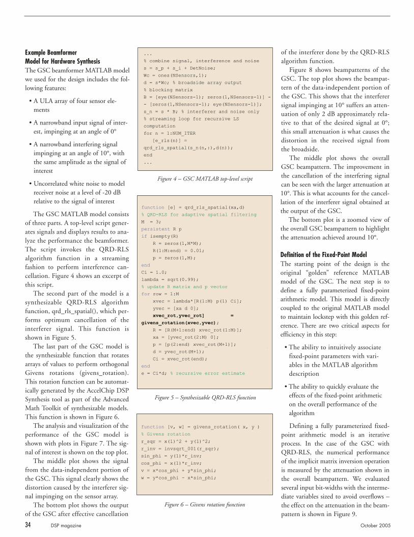
34 DSP magazine October 2005
Example Beamformer Model for Hardware SynthesisThe GSC beamformer MATLAB modelwe used for the design includes the fol-lowing features:
• A ULA array of four sensor ele-ments
• A narrowband input signal of inter-est, impinging at an angle of 0°
• A narrowband interfering signalimpinging at an angle of 10°, withthe same amplitude as the signal ofinterest
• Uncorrelated white noise to modelreceiver noise at a level of -20 dBrelative to the signal of interest
The GSC MATLAB model consistsof three parts. A top-level script gener-ates signals and displays results to ana-lyze the performance the beamformer.The script invokes the QRD-RLSalgorithm function in a streamingfashion to perform interference can-cellation. Figure 4 shows an excerpt ofthis script.
The second part of the model is asynthesizable QRD-RLS algorithmfunction, qrd_rls_spatial(), which per-forms optimum cancellation of theinterferer signal. This function isshown in Figure 5.
The last part of the GSC model isthe synthesizable function that rotatesarrays of values to perform orthogonalGivens rotations (givens_rotation).This rotation function can be automat-ically generated by the AccelChip DSPSynthesis tool as part of the AdvancedMath Toolkit of synthesizable models.This function is shown in Figure 6.
The analysis and visualization of theperformance of the GSC model isshown with plots in Figure 7. The sig-nal of interest is shown on the top plot.
The middle plot shows the signalfrom the data-independent portion ofthe GSC. This signal clearly shows thedistortion caused by the interferer sig-nal impinging on the sensor array.
The bottom plot shows the outputof the GSC after effective cancellation
of the interferer done by the QRD-RLSalgorithm function.
Figure 8 shows beampatterns of theGSC. The top plot shows the beampat-tern of the data-independent portion ofthe GSC. This shows that the interferersignal impinging at 10° suffers an atten-uation of only 2 dB approximately rela-tive to that of the desired signal at 0°;this small attenuation is what causes thedistortion in the received signal fromthe broadside.
The middle plot shows the overallGSC beampattern. The improvement inthe cancellation of the interfering signalcan be seen with the larger attenuation at10°. This is what accounts for the cancel-lation of the interferer signal obtained atthe output of the GSC.
The bottom plot is a zoomed view ofthe overall GSC beampattern to highlightthe attenuation achieved around 10°.
Definition of the Fixed-Point ModelThe starting point of the design is theoriginal “golden” reference MATLABmodel of the GSC. The next step is todefine a fully parameterized fixed-pointarithmetic model. This model is directlycoupled to the original MATLAB modelto maintain lockstep with this golden ref-erence. There are two critical aspects forefficiency in this step:
• The ability to intuitively associatefixed-point parameters with vari-ables in the MATLAB algorithmdescription
• The ability to quickly evaluate theeffects of the fixed-point arithmeticon the overall performance of thealgorithm
Defining a fully parameterized fixed-point arithmetic model is an iterativeprocess. In the case of the GSC withQRD-RLS, the numerical performanceof the implicit matrix inversion operationis measured by the attenuation shown inthe overall beampattern. We evaluatedseveral input bit-widths with the interme-diate variables sized to avoid overflows –the effect on the attenuation in the beam-pattern is shown in Figure 9.
...
% combine signal, interference and noise
s = s_p + s_i + DetNoise;
Wc = ones(NSensors,1);
d = s*Wc; % broadside array output
% blocking matrix
B = [eye(NSensors-1); zeros(1,NSensors-1)] -
- [zeros(1,NSensors-1); eye(NSensors-1)];
s_n = s * B; % interferer and noise only
% streaming loop for recursive LS
computation
for n = 1:NUM_ITER
[e_rls(n)] =
qrd_rls_spatial(s_n(n,:),d(n));
end
...
function [e] = qrd_rls_spatial(xa,d)
% QRD-RLS for adaptive spatial filtering
M = 3;
persistent R p
if isempty(R)
R = zeros(1,M*M);
R(1:M:end) = 0.01;
p = zeros(1,M);
end
Ci = 1.0;
lambda = sqrt(0.99);
% update R matrix and p vector
for row = 1:M
xvec = lambda*[R(1:M) p(1) Ci];
yvec = [xa d 0];
xvec_rot,yvec_rot] =
givens_rotation(xvec,yvec);
R = [R(M+1:end) xvec_rot(1:M)];
xa = [yvec_rot(2:M) 0];
p = [p(2:end) xvec_rot(M+1)];
d = yvec_rot(M+1);
Ci = xvec_rot(end);
end
e = Ci*d; % recursive error estimate
function [v, w] = givens_rotation( x, y )
% Givens rotation
r_sqr = x(1)^2 + y(1)^2;
r_inv = invsqrt_001(r_sqr);
sin_phi = y(1)*r_inv;
cos_phi = x(1)*r_inv;
v = x*cos_phi + y*sin_phi;
w = y*cos_phi - x*sin_phi;
Figure 4 – GSC MATLAB top-level script
Figure 5 – Synthesizable QRD-RLS function
Figure 6 – Givens rotation function

We selected a 16-bit implementationthat achieves an almost ideal interferencerejection, as shown in Figure 9.
Generation of Hardware ImplementationThe final step in our methodology is togenerate the hardware implementation.There are two critical aspects to achieveefficiency:
• The ability to automatically generatean implementation that is bit-accu-rate against the fixed-point model ofthe DSP algorithm
• The ability to tailor the hardwarearchitecture of the implementationto meet area/speed requirements
The generation of a suitable hard-ware implementation is also done itera-tively to balance resource utilizationand speed of operation. For the QRD-RLS algorithm, there are two pointswhere the area/speed of the implemen-tation can be affected:
• Controlling the degree of resourcesharing of the givens_rotationfunction
• The rotation of row elements inthe Givens rotation function canbe achieved with different compu-tation styles, including Newton-Raphson (using multipliers) andCORDIC (multiplier-less) micro-architectures
We performed iterations of this stepexploring different combinations ofresource utilization and speed of oper-ation of the QRD-RLS function. Theresults of RTL synthesis, summarizedin Table 1, are for a Xilinx Virtex-4XC4VSX55 target device.
The results indicate a smalldecrease in resource utilization (LUTs)with sequential implementations.With a goal of maximum speed ofoperation and a minimum use of hard-ware multipliers, the CORDIC paral-lel implementation was picked for theplace and route of the netlist fromRTL synthesis. The results of theimplementation using the XilinxISE™ software mapped to the sametarget device as during synthesis areshown in Table 2.
The hardware implementationresults show that the QRD-RLS func-tion can be implemented in 12% ofthe logic resources of a XC4VSX55device with a sustainable data rate of1.7 megasamples per second.
ConclusionYou can create an efficient hardwareimplementation of DSP algorithms inXilinx FPGAs using matrix inversionoperations with fixed-point arithmetic.The efficiency with which you canimplement these algorithms is based onthe use of the AccelChip DSP Synthesistool to enable a high level of automa-tion. The results show the effectivenessof this methodology in the implemen-tation of a challenging algorithm infixed-point arithmetic hardware.
To get more information aboutAccelChip’s solutions, visit www.accelchip.com. For a list of other techni-cal papers from AccelChip, visitwww.accelchip.com/papers.
This article is based on the paper, “EfficientMethodology for Implementation of MatrixInversion in Fixed-Point Hardware,” pre-sented at the 2005 GSPx Conference.
Metric Multiplier Parallel Multiplier Sequential CORDIC Parallel CORDIC Sequential
LUTs 5% 4% 10% 9%
DSP48s 51 19 1 1
Sustainable Data Rate 1.9 MSPS 0.8 MSPS 1.8 MSPS 0.18 MSPS
Occupied Slices 3076 (12%)
DSP48s 1
Sustainable Data Rate 1.7 MSPS
October 2005 DSP magazine 35
Figure 7 – GSC time-domain signals
Figure 8 – GSC beampatterns
Figure 9 – GSC beampattern in fixed point
Table 1 – RTL synthesis results Table 2 – Implementation results


by Eric Cigan Product Marketing Manager AccelChip Inc. [email protected]
Narinder LallSenior DSP Marketing ManagerXilinx, [email protected]
There are two kinds of people in electronicdesign: those who think in terms of wordsand those who think in terms of pictures.This dichotomy is most appar-ent in the world of DSP. Somedesigners prefer to developalgorithms in language form,while others choose to draw outblock diagrams showing dataflows. Until now, different setsof tools were required for eachmethod – but why should youhave to choose?
Xilinx® System Generatorfor DSP is well established as aproductive tool for creatingDSP designs using graphicalmethods. With a visual pro-gramming environment thatleverages The MathWorksSimulink tool and its prede-fined Xilinx block set of DSPfunctions, System Generatormeets the needs of both sys-tem architects (to integratedesign components) and hard-ware designers (to optimizeimplementations). (For moredetails, see “Implementing
DSP Algorithms in FPGAs” in theWinter 2004 issue of the Xcell Journal.)
Many DSP algorithm developers havefound that the MATLAB language bestmeets their preferred development style.With more than 1,000 built-in functions, aswell as toolbox extensions for signal process-ing, communications, and wavelet process-ing, MATLAB offers a rich environment foralgorithm development and debugging.
In addition to the IP functions pro-vided in MATLAB, the MATLAB lan-
guage is uniquely adept with vector- andarray-based waveform data at the core ofalgorithms in applications such as wire-less communications, radar/infraredtracking, and image processing.
The AccelChip DSP Synthesis tool wasdeveloped specifically for algorithm devel-opers and DSP architects who haveembraced a language-based flow. WithAccelChip, you begin with MATLAB M-files to perform stimulus creation, algo-rithm evaluation, and post-processing.
You can load the M-files intothe AccelChip tool; theybecome the “golden source” fora design flow that ultimatelyproduces optimized implemen-tations in Xilinx FPGAs.
Unifying Words and PicturesIn the past, design teamslooked on System Generatorand AccelChip DSP Synthesisas mutually exclusive designtool options, but wished foraccess to the best aspects ofeach tool. In response,AccelChip and the DSP divi-sion at Xilinx collaborated in aneffort to combine AccelChip’stools with System Generator.The result allows you to mix language-based algorithmdesign in MATLAB and graph-ical block-oriented design inSimulink in a novel unifiedelectronic-system-level (ESL)design environment (Figure 1).
Integrating MATLAB Algorithmsinto FPGA DesignsIntegrating MATLAB Algorithmsinto FPGA Designs
October 2005 DSP magazine 37
The integration of AccelChip DSP Synthesisand Xilinx System Generator for DSP provides a seamless path from MATLAB/Simulink toverified FPGA-based DSP systems.
The integration of AccelChip DSP Synthesisand Xilinx System Generator for DSP provides a seamless path from MATLAB/Simulink toverified FPGA-based DSP systems.
Figure 1 – System Generator/AccelChip interface
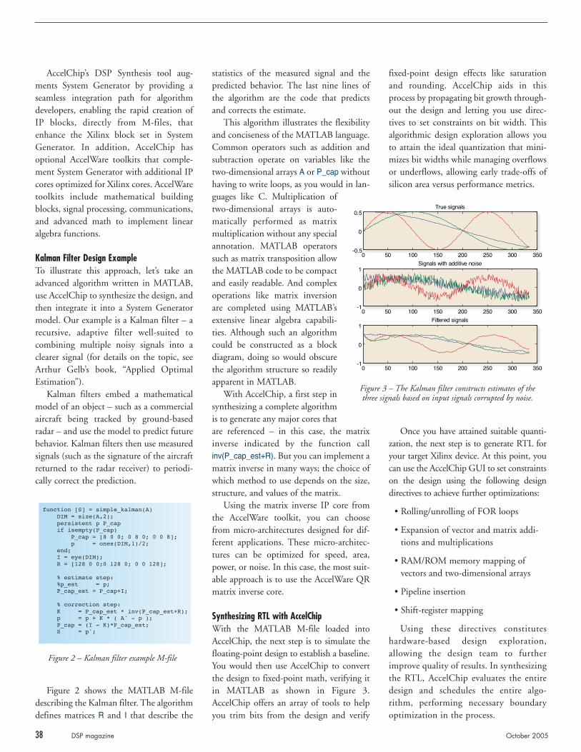
AccelChip’s DSP Synthesis tool aug-ments System Generator by providing aseamless integration path for algorithmdevelopers, enabling the rapid creation ofIP blocks, directly from M-files, thatenhance the Xilinx block set in SystemGenerator. In addition, AccelChip hasoptional AccelWare toolkits that comple-ment System Generator with additional IPcores optimized for Xilinx cores. AccelWaretoolkits include mathematical buildingblocks, signal processing, communications,and advanced math to implement linearalgebra functions.
Kalman Filter Design ExampleTo illustrate this approach, let’s take anadvanced algorithm written in MATLAB,use AccelChip to synthesize the design, andthen integrate it into a System Generatormodel. Our example is a Kalman filter – arecursive, adaptive filter well-suited tocombining multiple noisy signals into aclearer signal (for details on the topic, seeArthur Gelb’s book, “Applied OptimalEstimation”).
Kalman filters embed a mathematicalmodel of an object – such as a commercialaircraft being tracked by ground-basedradar – and use the model to predict futurebehavior. Kalman filters then use measuredsignals (such as the signature of the aircraftreturned to the radar receiver) to periodi-cally correct the prediction.
Figure 2 shows the MATLAB M-filedescribing the Kalman filter. The algorithmdefines matrices R and I that describe the
fixed-point design effects like saturationand rounding. AccelChip aids in thisprocess by propagating bit growth through-out the design and letting you use direc-tives to set constraints on bit width. Thisalgorithmic design exploration allows youto attain the ideal quantization that mini-mizes bit widths while managing overflowsor underflows, allowing early trade-offs ofsilicon area versus performance metrics.
Once you have attained suitable quanti-zation, the next step is to generate RTL foryour target Xilinx device. At this point, youcan use the AccelChip GUI to set constraintson the design using the following designdirectives to achieve further optimizations:
• Rolling/unrolling of FOR loops
• Expansion of vector and matrix addi-tions and multiplications
• RAM/ROM memory mapping of vectors and two-dimensional arrays
• Pipeline insertion
• Shift-register mapping
Using these directives constituteshardware-based design exploration,allowing the design team to furtherimprove quality of results. In synthesizingthe RTL, AccelChip evaluates the entiredesign and schedules the entire algo-rithm, performing necessary boundaryoptimization in the process.
statistics of the measured signal and thepredicted behavior. The last nine lines ofthe algorithm are the code that predictsand corrects the estimate.
This algorithm illustrates the flexibilityand conciseness of the MATLAB language.Common operators such as addition andsubtraction operate on variables like thetwo-dimensional arrays A or P_cap withouthaving to write loops, as you would in lan-guages like C. Multiplication oftwo-dimensional arrays is auto-matically performed as matrixmultiplication without any specialannotation. MATLAB operatorssuch as matrix transposition allowthe MATLAB code to be compactand easily readable. And complexoperations like matrix inversionare completed using MATLAB’sextensive linear algebra capabili-ties. Although such an algorithmcould be constructed as a blockdiagram, doing so would obscurethe algorithm structure so readilyapparent in MATLAB.
With AccelChip, a first step insynthesizing a complete algorithmis to generate any major cores thatare referenced – in this case, the matrixinverse indicated by the function callinv(P_cap_est+R). But you can implement amatrix inverse in many ways; the choice ofwhich method to use depends on the size,structure, and values of the matrix.
Using the matrix inverse IP core fromthe AccelWare toolkit, you can choosefrom micro-architectures designed for dif-ferent applications. These micro-architec-tures can be optimized for speed, area,power, or noise. In this case, the most suit-able approach is to use the AccelWare QRmatrix inverse core.
Synthesizing RTL with AccelChipWith the MATLAB M-file loaded intoAccelChip, the next step is to simulate thefloating-point design to establish a baseline.You would then use AccelChip to convertthe design to fixed-point math, verifying itin MATLAB as shown in Figure 3.AccelChip offers an array of tools to helpyou trim bits from the design and verify
38 DSP magazine October 2005
function [S] = simple_kalman(A) DIM = size(A,2); persistent p P_cap if isempty(P_cap) P_cap = [8 0 0; 0 8 0; 0 0 8]; p = ones(DIM,1)/2; end; I = eye(DIM); R = [128 0 0;0 128 0; 0 0 128];
% estimate step: %p_est = p; P_cap_est = P_cap+I;
% correction step: K = P_cap_est * inv(P_cap_est+R); p = p + K * ( A' - p ); P_cap = (I - K)*P_cap_est; S = p';
0 50 100 150 200 250 300 350-0.5
0
0.5True signals
0 50 100 150 200 250 300 350-1
0
1Signals with additive noise
0 50 100 150 200 250 300 350-1
0
1Filtered signals
Figure 2 – Kalman filter example M-file
Figure 3 – The Kalman filter constructs estimates of thethree signals based on input signals corrupted by noise.

Throughout this flow, AccelChip main-tains a uniform verification environmentthrough a self-checking test bench; theinput/output vectors that were generatedwhen verifying the fixed-point MATLABdesign are used to verify the generatedRTL. The RTL verification step also givesAccelChip the information necessary tocompute the throughput and latency of theKalman filter. This is essential informationto assess whether the design meets specifi-cations and is critical for achieving cycle-accurate simulation.
Exporting from AccelChip to System GeneratorAlthough RTL verification is a key step inthe design flow, designers want to see algo-rithms running in hardware. SystemGenerator’s hardware-in-the-loop co-simu-lation interfaces make this a push-buttonflow, allowing you to bring the full powerof MATLAB and Simulink analysis func-tions to hardware verification.
Now that you have run RTL verifica-tion in AccelChip, you are ready to exportthe AccelChip design to System Generatorby going to the “Export” pull-down menuin the AccelChip GUI and selecting“System Generator.” AccelChip then gen-erates a cycle-accurate System Generatorblock that supports both simulation andRTL code generation.
At this point, you transition the designflow to System Generator, where a new
block for the Kalman filter is available inthe Simulink library browser. You needonly select the Kalman filter block and dragit into the destination model to incorporatethe AccelChip-generated Kalman filter intoa System Generator design.
Figure 4 shows the resulting diagram forthe Kalman filter. In the center of theSystem Generator diagram is the Kalmanfilter, and around it are the gateway blocksneeded for a System Generator design.
Once the AccelChip-generated block isincluded in the System Generator design,you can perform a complete, system-levelsimulation of cycle-accurate, bit-true mod-els to verify that the system meets specifica-tions. You can use AccelChip-generatedblocks for System Generator in conjunc-tion with the Xilinx block set. Once thissystem-level verification step is completed,the next step in the System Generator flowis to move on to design implementation.The “Generate” step in System Generatorcompiles the design into hardware.
Verification OptionsAll design files generated by AccelChip,including exported System Generator files,are verified back to the original “golden”source MATLAB M-file. AccelChip’s veri-fication approach is based on the genera-tion of a test bench from the MATLABsource – this test bench is applied at theRTL level within AccelChip and can be
applied in System Generator to verify thecorrectness of the design.
Once verified in the System Generatorenvironment, you can verify theAccelChip-generated block using SystemGenerator’s supported methods – includ-ing HDL co-simulation and hardware-in-the-loop – to accelerate hardware-levelsimulation 10 to 100 times.
ConclusionThe integration of AccelChip withXilinx System Generator is the first solu-tion to unite MATLAB-based algorith-mic synthesis favored by algorithmdevelopers with the graphical design flowused by system architects and hardwaredesigners. It uses the rich MATLAB lan-guage and its companion toolboxes tocreate System Generator IP blocks ofcomplex DSP algorithms.
By using these tools together, designteams can employ the most productivemeans of modeling hardware for imple-mentation, fully involving algorithmdevelopers in the FPGA design processand completing higher quality designsmore quickly.
For more information on AccelChip and its interface to Xilinx SystemGenerator, visit www.accelchip.com. Formore information on System Generator,visit www.xilinx.com/products/design_resources/dsp_central/grouping/index.htm.
October 2005 DSP magazine 39
a_in_3
a_in_2
a_in_1
s_3
s_2
s_1
kalman_filter_wrappers-model_kalman_filter_wrapper
Step
Sine Wave2
Sine Wave1
Sine Wave
Scope4
Scope3
Scope2 Scope
[ac_reset]
Goto
fpt dbl
Gateway Out2
fpt dbl
Gateway Out1
fpt dbl
Gateway Out
dbl fpt
Gateway In3
dbl fpt
Gateway In2
dbl fpt
Gateway In1
dbl fpt
Gateway In
Band-LimitedWhite Noise2
Band-LimitedWhite Noise1
Band-LimitedWhite Noise
Sy stemGenerator
Figure 4 – AccelChip exports a cycle-accurate System Generator block that supports both simulation and RTL code generation.

by Manuel UhmSenior Marketing ManagerXilinx, [email protected]
Software-defined radios (SDRs) havealready become a reality in the defenseindustry through programs such as theJoint Tactical Radio System (JTRS).Because SDRs are already being deployed,why would a new architectural paradigmbe of interest? The reason is simple: thepower consumption and cost of first-gener-ation SDRs is generally too high for wide-spread deployment.
Despite Moore’s Law, incremental processimprovements are not sufficient to reach thepower and cost restrictions for small-form-factor, handheld, and manpack radios, suchas those required for JTRS Cluster 5. Inaddition, architectural changes are requiredto reach the strenuous requirements.
Using partially reconfigurable platformFPGAs as an SDR system-on-chip (SoC)addresses both of these issues by decreasingthe number of DSP components in an
SDR while still providing the necessaryfunctionality. In this article, I’ll discusshow to apply this revolutionary technologyto an SDR black-side modem.
Architectural Improvement #1: SCA-Enabled SDR SoCCurrent SDR modem architectures, such asthat of JTRS Cluster 1, utilize a discrete gen-eral-purpose processor (GPP) to manage theapplication and control infrastructure,known as the Software CommunicationsArchitecture (SCA) Operating Environment(OE). The GPP is coupled with an FPGAfor channelization and wideband waveformprocessing and a DSP for narrowband wave-form processing.
The SCA OE comprises a POSIX-com-pliant real-time operating system (RTOS)for scheduling and memory protection, aCORBA (Common Object Request BrokerArchitecture) ORB for message passing, andan SCA Core Framework (CF) for loadingand tearing down waveforms.
With the availability of platformFPGAs such as Xilinx® Virtex™-II Pro
and Virtex-4 FX devices that incorporatea hard-core PowerPC™ 405 GPP, it isnow possible to run the entire SCA OEin the same FPGA that is required in themodem for channelization and widebandwaveform processing. Because the 405has a memory management unit(MMU), it is possible to run a full RTOSand ensure memory protection, unlike asoft-core GPP. This results in an SCA-enabled SDR SoC.
I/O accounts for the most power con-sumption in an SDR modem; thus it isimportant to reduce the I/O count asmuch as possible. Removing the discreteGPP from the modem does just this, there-by having the primary benefit of reducingthe power consumption of the modem.Furthermore, the 405 hard-core is power-efficient, providing 600 DMIPS at 0.4W.
Secondary benefits include potentiallylower cost by the removal of the discreteGPP and a reduced signal processing foot-print, which can result in a smaller formfactor or better thermal dissipationthrough superior board layout.
Software-Defined Radio: The New Architectural ParadigmSoftware-Defined Radio: The New Architectural Paradigm
40 DSP magazine October 2005
Reduce system power and cost with a shared resources SoC.Reduce system power and cost with a shared resources SoC.

Architectural Improvement #2: Shared ResourcesThe current architecture for implement-ing an SDR modem is known as a dedi-cated resources model. It is calleddedicated resources because a set of pro-cessing resources is dedicated to a radiochannel (where each channel is capable ofrunning a waveform, such as the SingleChannel Ground and Airborne RadioSystem [SINCGARS]). In this case, theprocessing resources consist of an A/D,D/A, FPGA, DSP, and GPP. To imple-ment an N-channel radio, N sets of pro-cessing resources are required. This isillustrated in Figure 1 for a four-channelSDR modem supporting an SCA CF.
From a functional perspective, thisarchitecture is sufficient for radios with lesspower and size-constrained environments,such as Cluster 1 vehicular radios.However, it is an inefficient usage of theavailable processing resources, resulting inexcess power consumption and cost. Forexample, the signal processing parts for allchannels of the radio must be selected forthe worst-case scenario; the processingresources must be able to support thelargest waveform (WNW, the WidebandNetworking Waveform) such that if only asmall narrowband waveform like SINC-GARS is instantiated, most of that chan-nel’s processing resources are not utilized.This has a significant impact on driving up
ed is a function of the size of the waveformand the size of the available processingresources. Figure 2 illustrates how a multi-channel SCA-enabled SDR modem couldbe implemented using this architecture. Inthis instance, the signal processing partcount has decreased from 20 to 4 compo-nents. Hence, implementation of thesearchitectural advantages can result in a pro-duction cost and power consumption thatis two to three times lower than the dedi-cated resources model.
You will also notice that the FPGA iscapable of doing all the heavy digital signalprocessing. The embedded GPP is also anatural fit for the light signal processing,such as synchronization loop control, aswell as the upper protocol layers such aslink and network layers.
It is also worth noting that both archi-tectures illustrated here are using 100%commercially available components. In theshared resources model, the SoC FPGA canbe a mid- to large-sized Virtex-II Pro orVirtex-4 FX FPGA with an embeddedPowerPC core.
Partial Reconfiguration: The Enabling TechnologyThe technology that enables the sharedresources model is partial reconfigurationof the FPGA. Partial reconfigurationenables an application or component, suchas a waveform or waveform component, to
the cost of the modem. Obviously, theproblem gets exacerbated as you scale themodel further. JTRS AMF (the JTRSCluster for Airborne, Maritime, and Fixedinstallations) requires some radios to sup-port eight channels. This also has animpact on power consumption.
A more efficient architecture for an SDRmodem is referred to as a shared resourcesmodel. Unlike a dedicated resources model,this architecture offers the capability to sup-port multiple waveforms across a single setof processing resources, allowing for muchmore efficient usage of the resources. Thenumber of waveforms that can be support-
October 2005 DSP magazine 41
Waveform D
Waveform C
Waveform B
Waveform A Waveform Control
A/D
D/A
FPGA DSP GPP
FPGA Functions• Channelization• DSP
DSP Functions• Mod/Demod• FEC
GPP Functions• SCA CF• CORBA• RTOS• DSP
GPP Functions• SCA CF• CORBA/RTOS• DSP
FPGA Functions• Channelization• DSP
Waveform Control
Narro
wb
and
Wavefo
rm
Narro
wb
and
Wavefo
rm
Narro
wb
and
Wavefo
rm
Narro
wb
and
Wavefo
rm
Wid
eban
d W
aveform
(i.e., WN
W)
A/D
D/A
Embedded
GPPEmbedded
GPP
FPGA FPGA
SERDES
Figure 2 – A multi-channel SCA-enabled SDR modem architecture using a shared resources model. In this example, 5 channels supporting 1 wideband waveform and
4 narrowband waveforms have been implemented, while reducing the signal processing part count from 20 to 4 components compared to a dedicated resources model.
Figure 1 – Current SCA-enabled SDR modems use a dedicated set of signal processing hardware for each channel. The more channels the SDR must support, the more hardware
it contains. This has a direct impact on power consumption and cost.

42 DSP magazine October 2005
be dynamically loaded or unloaded in aportion of the device while other portionsare either being used by other applicationsor going unused. This allows support formultiple independent applications concur-rently in a single FPGA, which is some-what analogous to dynamic task switchingof a GPP. Without this capability, it wouldbe necessary to reconfigure the entireFPGA to support a different application,which would result in the loss ofall previous applications.
For example, if an FPGA wasconfigured to support a SAT-URN comm link, it would haveto be fully reconfigured to sup-port an HAVEQUICK commlink, therefore resulting in theloss of the SATURN link regard-less of how much leftover logicthere was in the FPGA. Clearlythis is unacceptable for a radio.Furthermore, partial reconfigu-ration enables an adaptive wave-form to be supported in asmaller FPGA because theFPGA can dynamically load andswitch between waveform com-ponents, rather than having allpossible waveform componentsloaded at runtime.
Three basic elements arerequired to support partialreconfiguration in an FPGA:
1. An FPGA that inherentlysupports partial reconfigura-tion, such as the Xilinx Virtexfamily. The Virtex family isframe-reconfigurable, meaning thatindividual frames of logic within thedevice can be dynamically reconfiguredindependent of the rest of the frames. InVirtex-II Pro devices, a frame consists ofa column, while in Virtex-4 FPGAs, aframe consists of a 16 x 1 configurablelogic block (CLB) “tile.”
2. At least a basic controller must be avail-able to dynamically manage the recon-figuration of the FPGA. This could bean embedded GPP, a soft-core GPP(such as the Xilinx MicroBlaze™processor core), or an external GPP con-
nected to the FPGA. In the sharedresources model example, the sameembedded GPP that is running the SCAOE is also managing the partial recon-figuration of the FPGAs.
3. Partial reconfiguration software develop-ment tools that support the develop-ment of applications, restricted toboundaries complying with the hard-ware architecture of the FPGA.
Although elements #1 and #2 have beenaround for some time, it is only recently thatsoftware development tools enabling partialreconfiguration design have become avail-able. Standard tools from Xilinx are availableby request for Virtex-II Pro today and forVirtex-4 in the fourth quarter of 2005.
Implementing the ArchitectureThe shared resources model using an SCA-enabled SoC has been proven to worktoday in a COTS (commercial-off-the-shelf ) Xilinx Virtex-II Pro-based SDRmodem from ISR Technologies. Thedemonstration system uses two modems,
each supporting two independent applica-tions: a narrowband, 256 Kbps waveformsupporting a comm link between two VoIPphones; and a wideband, 1,024 Kbps wave-form supporting a streaming video linkbetween two laptops.
Using a COTS SCA CF from theCommunications Research Centre, the videolink can be instantiated and torn down whilemaintaining the comm link – and vice versa.
More details on the demon-stration can be found in the December 2004 JTRSJPO Technology AwarenessBulletin, published by theJTRS Joint Program Office athttp://jtrs.army.mil/sections/t e c h n i c a l i n f o r m a t i o n /fset_technical.html.
Figure 3 illustrates thefloorplan of the Virtex-II Prodevice in each of themodems. The yellow areasrepresent static infrastruc-ture, as they do not changeregardless of the waveformsbeing supported. Thisincludes the digital downand up converter, internalshared buses (the CoreConnect bus for the embed-ded PowerPC 405) and theinterfaces to external devices,such as the A/D and D/A.The two applications (wave-form A and B) run inde-pendently in the partiallyreconfigurable region in the
right-hand side of the device. If necessary,a larger waveform or more smaller wave-forms could run in the same space.
ConclusionPower consumption and cost are issues thatare preventing widespread deployment ofSDRs today, particularly in size, weight,power, and cost-constrained environments.Architectures that incorporate SCA-enabled SDR SoCs and a shared resourcesmodel can help to address these issues byproviding the most efficient SDR modemimplementation, thereby driving down thepower and cost.
RJ45 – 100BT(Data)
RJ45 – 100BT(Voice)
RJ45 – 100BT(Ctlr)
Ethernet Switch
Ethernet Interface
405GPP
Core C
onnectB
us to 405 Core
Waveform
A
Waveform
B
Waveform Combiner
Interpolation Filter
TX NCO RX NCO
D/A Interface(14 bits – 300 MHz)
A/D Interface(12 bits – 200 MHz)
DAC ADC
Xilinx Virtex-II ProSCA-EnabledSDR SoC
Decimation Filter
Figure 3 – Floorplan of a Xilinx Virtex-II Pro-based SCA-enabled SDR SoC suporting shared resources through partial reconfiguration. The yellow areas
represent static infrastructure and do not change from waveform to waveform, whereas the rest of the FPGA is available for partially reconfigured applications.

Traquair Data Systems, Inc. Tel: 607-266-6000 Email: [email protected] Web: www.traquair.com
micro-line C6713Compact
Embedded DSP/FPGA board
The micro-line C6713Compact is a high performance single board DSP/FPGA
solution, offering exceptional capabilities and flexibility.
Texas
Instruments’ most powerful floating point DSP processor, the TMS320C6713,
as well as with
xtensive digital I/O capabilities for easy integration with the on-board
FPGA, DSP and FireWire resources.
Measuring only 67 x 120mm, it combines a Xilinx Virtex-II FPGA with
up to 64MBytes of SDRAM, 8MBytes of FLASH ROM, FireWire,
and optional Ethernet communications and analog I/O.
It is suitable for stand-alone operation or as a mezzanine daughter card, and
has e
TMS320C6713 DSP
Up to 2400MIPS/1800 MFLOPS
Virtex-II FPGA
250k, 500k or 1MGates
IEEE 1394 FireWire
400MBit/sec Communications
IIDC DCAM Video Framecaputre
Optional Ethernet
10/100BaseT,
TCP/IP, UDP, ICMP, IGMP, Telnet,
HTTP, SMTP, POP3, FTP ,
Embedded Web Server
Optional Analog I/O
12/14/16-bit multi-channel A/D/A
via FPGA I/O Pins or DSP EMIF
The Compact DSP & FPGA Solution
Optional Data Storge
HD or Compact FLASH
FAT32 Filesystem Support

by Ken SienskiPresidentRed [email protected]
Established in 1996, Red River specializesin high-performance signal processing anddata communication solutions for theembedded systems market, especially soft-ware defined radio applications.
Our main challenge in serving the soft-ware defined radio market is to have a hard-ware platform that meets the demands ofmultiple configurations. Some customersare looking for a complete, pre-built radiosolution; others are looking to add customfeatures to a radio platform. These disparaterequirements place great demands on us tofind a common programmable silicon solu-tion that meets both needs.
The Xilinx® Virtex-4™ FPGA family
allows us to do exactly that – provide differ-ent customer solutions at the lowest cost.Advanced features such as FIFO logic,embedded PowerPC™, RocketIO™ trans-ceivers, and Ethernet MAC, as well asadvanced power and packaging technology,makes Virtex-4 devices a perfect choice for us.
Model 351 (Pocket Change)Our next-generation product, the Model351, or “Pocket Change,” transforms anyportable computer into a high-performancemulti-channel software defined radiotransceiver. The Pocket Change CardBusPC Card accepts two analog input signalsthrough MMCX coaxial connectors onthe outside edge of the card. The receiverinput is AC-coupled to a 14-bit (80MSPS) A/D converter. The transmitteroutput is supplied through a 14-bit (100 MSPS) D/A converter. Most of the
digital logic is supplied using a Virtex-4FPGA device.
When we began developing the Model351, we investigated various offerings onthe market and finally decided to useVirtex-4 FPGAs. The Virtex-4 FPGA fam-ily provides the flexibility and features thatsupport both our needs and the require-ments of our customers.
The Model 351 design comprises aVirtex-4 FPGA connected to an A/D con-verter, a D/A converter, and a dedicated PCIbus controller (for the CardBus interface tothe host computer) (Figure 1). Although it istargeted at our traditional software definedradio customers, the Model 351 is also suit-able for signal acquisition or generation, sig-nal intelligence collection, transceivermodem algorithm prototyping, frequencyhop signal generation, or portable signalrecorder/playback applications.
Virtex-4 FPGAs for Software Defined RadioVirtex-4 FPGAs for Software Defined Radio
44 DSP magazine October 2005
Red River’s new PCMCIA Type II module can transform any notebook computer into a software defined radio using a Virtex-4 FPGA for performance-critical DSP functions.
Red River’s new PCMCIA Type II module can transform any notebook computer into a software defined radio using a Virtex-4 FPGA for performance-critical DSP functions.

Customization and FlexibilityInitially we considered using dedicated dig-ital upconverter/downconverter chips toimplement the Model 351 transceiverfunction. However, many of our customersprefer the flexibility of inserting customfunctions into their designs. The cus-tomization requirement pushed us to useprogrammable technology.
By selecting a leading programmablelogic architecture, we can address the cus-tomization needs of a broad set of cus-tomers. Xilinx ISE™ developmentsoftware provides our customers a familiardesign environment to embed custom DSPfunctions in the uncommitted logic of theVirtex-4 FPGA.
Another benefit from using Virtex-4FPGAs is that we can offer multiple prod-ucts using one common hardware plat-form. This has helped reduce hardwaredevelopment time and simplify inventorymanagement.
Power and Space EfficiencyOne of the challenges in CardBus PC Carddevelopment is to select a device that meetsthe PCMCIA functional specification andthe tight power restriction of 3.3W. Wewere impressed with the power efficiencyof the Virtex-4 family, as it consumes halfthe power of comparable logic solutions.
Virtex-4 FPGAs give us significant fea-tures and performance while still meetingthe tight power budget of our design. Inaddition, PCMCIA imposes severe heightrestrictions in order to fit into the Type IImodule form factor. The Virtex-4 FF668package offering is one of the few FPGApackages that meet the height requirements.
the highest-performance internal blockRAM and unique integrated FIFO logic,Virtex-4 FPGAs give us the FIFO quanti-ty and performance that we need to keepup with the bandwidth of the analogcomponents and host interface.
Three Platforms Satisfy Multiple RequirementsThe three Virtex-4 platforms (LX, SX, andFX) give us unique capabilities for severalupcoming products. For customers want-ing to add custom logic functionality, weuse the LX platform. LX offers the choiceof many different gate densities within thesame package footprint, allowing us to usethe same base design to support many dif-ferent customer needs.
We have some designs that necessitatetremendous additional DSP capabilityfor math-intensive processing, includingsignal modulation and demodulation.For these applications, we see the SXplatform as a natural fit. SX devices give us by far the largest amount of DSPperformance.
For some of our other designs, we areimplementing the advanced system-levelblock functionality of the FX platform –PowerPC running VxWorks, RocketIOtransceivers for optical and PCI Expressinterfacing, and gigabit Ethernet MACcores. Because Virtex-4 devices give usthree platforms to choose from, we canoffer different capabilities across ourproduct line.
ConclusionSoftware defined radio products mustaddress a broad application space, whichpresents a challenge when selecting com-ponent features. The three Virtex-4 plat-forms give us the feature choice andperformance that we require to field afamily of solutions for both fixed andmobile installations.
The upcoming Model 351 demon-strates cutting-edge capabilities in anextremely small, power-efficient modulethat operates in a standard notebook com-puter. Visit www.red-river.com for moreinformation about the Model 351 andother Red River products.
Advanced Features and PerformanceOne key requirement for a software definedradio application is high-performance DSPcapability. The performance requirement isdriven by the need to support multiple sig-nal channels in real time.
Virtex-4 FPGAs are capable of perform-ing multi-channel digital upconversion anddownconversion across the entire Model351 analog bandwidth. The Virtex-4device can also perform Fast FourierTransforms (FFTs) for spectral analysis ofincoming signal data.
The Virtex-4 FPGA provides the “heavylifting” to process digital informationbetween the host computer and the A/D orD/A converter. The signal processingpower comes directly from the SX plat-form. Virtex-4 devices can achieve high-DSP performance by taking advantage ofmassive parallelism within each FPGA. Formath-intensive algorithms (likeDUC/DDC applications in a softwaredefined radio), the high number of DSPslices – multiply/add/accumulate engines –that can run up to 500 MHz provides thekind of performance only previously avail-able in fixed ASIC technology.
Our designs also make extensive use ofthe internal block memories in the FPGAto provide multi-queue FIFO capabilities.The FIFOs are used to buffer databetween the A/D or D/A converters andthe local bus for DMA operations, provid-ing performance-intensive processingwithout involving the host CPU in mem-ory transfers. This gives our products theability to flexibly handle digital radio datawithout completely consuming the CPUperformance of the host computer. With
October 2005 DSP magazine 45
Xilinx Virtex-4 FPGAs
A/D
CardBusInterface
AnalogInput
ACCoupler
HostProcessor
A/D
and
D/A
Inte
rfac
e
D/AAC
Coupler
AnalogOutput
DigitalData/Control
Clock SelectExternalClock
Use
r-C
onfig
urab
le L
ogic
Loca
l Bus
Inte
rfac
e
ConfigurationFlashOscillator
Figure 1 – Model 351 block diagram
by Scott FergusonFactory Application Engineer, Logic AnalyzersAgilent Technologies, [email protected]
As FPGAs become a viable option for high-performance signal processing in the digitalcommunications design space (cellular basestations, satellite communications, andradar), analysis and debug tools mustinclude new techniques to help you get themost optimal performance in your circuitsin the least amount of time.
Although signal analysis tools that con-nect to simulation and RF analog signalsare available, it’s important to be able tomeasure signal quality (frequency spec-trum, I-Q constellation, and error vectormagnitude [EVM]) in the sub-circuits ofyour FPGA. Thus, Agilent has linked its89601A Vector Signal Analysis (VSA) soft-ware with its line of logic analyzer products(1680, 1690, and 16900 families) to createa digital VSA tool. This tool, when com-bined with the Xilinx® ChipScope™ ProAgilent Trace Core, allows you to performsignal analysis anywhere inside your FPGAdesign quickly and easily.
In this article, we’ll show how this com-bination of tools works – and how it canhelp you get the most from your Xilinx-based DSP circuits.
Real-Time Analysis of DSP DesignsReal-Time Analysis of DSP Designs
46 DSP magazine October 2005
Agilent combines the FPGA Dynamic Probe and digital VSA.Agilent combines the FPGA Dynamic Probe and digital VSA.

Digital VSAVSA uses Fast Fourier Transform (FFT)-based data processing to provide a combi-nation of time- and frequency-domaindisplays and measurements. Figure 1shows a typical VSA display. Althoughthe display is extremely flexible and con-figurable, the main components includethe I-Q constellation plot (upper left),magnitude spectrum (lower left), errorvector (upper right), and measurements(lower right). The EVM is displayed inthe measurements section. This singlevalue is a key indicator of the quality ofthe modulated signal.
EVM is computed by extracting I-Qsymbols from the captured data; the sym-bols are the grid points in the constella-tion defined by the QPSK, QAM, orother modulation scheme. Once extractedfrom the measured signal, the symbolsequence is used to create an ideal (theo-retically perfect) signal known as the “ref-erence” signal. Each measured signal iscompared to the reference signal, and thedifference is known as an error vector.(The error can contain both I and Q, ormagnitude and phase components). Theindividual error vectors for a single cap-ture are combined to make a single EVMmeasurement.
Although this analysis software wasoriginally created to analyze analog RFsignals, it was developed in a hardware-independent, PC-based software package.Because Agilent logic analyzers are alsoPC-based, it was easy to extend the VSAsoftware to link to the logic analyzers.
Digital baseband and IF signals are rep-resentations of analog signals. Rather thanusing an instrument that digitizes a signalto enable FFT analysis (like an RF signalanalyzer), the signal is digital from thestart. These digital versions of analog sig-nals can be displayed in a logic analyzer ina chart-style waveform, which resemblesan oscilloscope display (as in Figure 2).
As you can see, when the bus is syn-chronously sampled and the sample ratemeets the Nyquist requirements, the logicanalyzer captures a sufficiently accurateversion of the “once-was” or “will-soon-be” analog signal.
core is a switching MUX incorporatedinto the design using the ChipScope ProCore Inserter, typically post-synthesis.During core insertion, you select theinternal nets to connect to the trace core,and the physical pads to which you willconnect the MUX output. These pads are
then routed on the circuit board toa logic analyzer probe.
The logic analyzer controls theFPGA through JTAG (downloadingthe bit file and selecting banks).When you select a new bank, thelogic analyzer automatically reconfig-ures itself to match the names of thenets now connected to the probe.
Design Example – QAM16 ModulatorWith help from our local XilinxDSP specialist FAE, we created ademo that fits into a small Virtex™-II part (XC2V250-FG256) usingXilinx System Generator for DSP.This tool makes creating DSPdesigns quick and easy. The design(shown in the block diagram inFigure 3) contains a 25 MHz symbolencoder; a root-raised cosine filterwith 24 taps and 4X interpolation(the output running at 100 MHz);and an IF modulation stage with a25 MHz local oscillator.
FPGA Dynamic ProbeThe FPGA Dynamic Probe, working withthe ChipScope Pro analyzer, can provideaccess to any part of a DSP design withoutrecompiling. In Figure 3, a simplified dig-ital radio transmitter design is connectedto the Agilent Trace Core 2 (ATC2). This
October 2005 DSP magazine 47
SymbolEncoder
BB Filter
BB Filter
IF LO
90 deg
0deg
Bank 0 Bank 1 Bank 2 Bank 3
MUX
Logic Analyzer Probe
JTAG
I
Select Signal Bankvia JTAG
Q
Figure 3 – FPGA Dynamic Probe
Figure 2 – Chart display of digital bus
Figure 1 – VSA display

Integrating the ATC2 Core in a System Generator DesignAfter compiling this design intoVHDL, we inserted the ATC2 core.To make the signal names more logi-cal on the logic analyzer display, wedid some hand-editing of the VHDL.(You could avoid this step by carefullychoosing net names in the SystemGenerator.) We then connected mostof the interesting nets as output portsfrom the top-level object to make thenet names short enough to fit on thelogic analyzer screen.
When connecting nets to outputports solely for use with the FPGADynamic Probe, a good trick is to usethe “keep” attribute in the VHDL.Because you don’t add the ATC2 coreto the design until after synthesis,many nets would otherwise be opti-mized out because they’re not con-nected to anything. In VHDL, thesyntax to use the “keep” attributelooks like this:
attribute keep : string;
attribute keep of i_symbol: signal is “true”;
attribute keep of q_symbol: signal is “true”;
We created an ATC2 core withfour banks, each with 48 signals.Using the ATC2 core’s 2X TDMoption (time-slicing two signals at atime on each pad), this requires only25 package pads on the FPGA (onefor a clock and 24 for data). This givesus access to 192 signals. Actually, weonly need to view about 92 signals:
• I-Q symbols, 8 bits each (16)
• I-Q filter output, 24 bits each (48)
• IF local oscillator sine and cosine,2 bits each (4)
• Combined IF signal (24)
The output of the RRC filter with24-bit I and Q signals was the largestrequirement, defining the number ofpins required. If 24 pins were notavailable, you could drop the least sig-
nificant bits, losing some dynamic rangebut still being able to view the signals.
Time-Domain, Logic, and VSA MeasurementsThe logic analyzer uses synchronoussampling (or “state mode”) to capturethe output of the ATC2 core. Thismeans that data is sampled on eachedge of the ATC2’s output clock. Ourdesign has two clock rates in the circuit– 25 MHz for the symbol data beforethe RRC filter and 100 MHz for allparts after the filter. Because the ATC2core supports only one clock per core,two options exist for debug:
• Using two cores, one for each clock rate
• Using one core with the fasterclock rate and over-sampling the25 MHz bus
Because the two clocks are correlated– and one is an integer multiple of theother – you can just over-sample theslower bus. If over-sampling is not desir-able, the logic analyzer can use a setupthat stores every fourth sample, therebycapturing the 25 MHz bus accuratelywith one sample per 25 MHz clock.
With the extra signals available inthe MUX, we were able to double-probe some of the interesting signals.For example, in bank 0 we have the Iand Q symbols before the filter, andalso the I component after the RRC fil-ter. This means we can do some time-domain analysis in the logic analyzer tomeasure group delay in the filter, as inFigure 4. Two markers indicate a com-mon signal feature: a wide, flat top andthe marker measurement display show-ing an interval of 250 ns.
After probing the interesting parts ofthe circuit, we performed vector signalanalysis on the signals and measured thequality of our RRC filter and IF modu-lation stages.
Looking at the QAM16 I-Q symbolsbefore they were filtered (as shown inFigure 5), you can see the 16-pointQAM constellation (upper left graph).
48 DSP magazine October 2005
Figure 7 – Digital IF signal
Figure 6 – Filtered IQ baseband data
Figure 5 – Unfiltered QAM16 symbols
Figure 4 – Filter group delay measurement

With one point per symbol, the linesbetween the constellation points arestraight. The frequency spectrum (in thelower left graph) is centered at 0 Hz andhas a 25 MHz pass-band with power inadjacent channels. Adjacent channel poweris undesirable in the RF signal, of course,which is the reason for the baseband filter.
By selecting a different bank in theATC2 core (controlled by the logic analyz-er), you can perform analysis on the IQ sig-nal after the baseband filter, as seen inFigure 6. Now the spectrum has sidebandsremoved, and the measurement display (inthe lower right quadrant) shows an EVMof 0.5%. The next time your RF team com-plains of errors in the baseband design, youcan point to this measurement (with whichthey are quite familiar), and prove that it’snot your filter’s fault.
In many digital radio designs, this IQsignal would now be converted to analog.However, we performed the IF modulationdigitally inside the same FPGA. Switchingbanks in the FPGA Dynamic Probe gives usaccess to the digital IF (again, withoutanother synthesis and place and route step),as shown in Figure 7. Note that the spec-trum and I-Q constellation are roughly thesame, only now centered about 25 MHz.The EVM is a little bit higher, indicatingthat you may want to use a higher qualitylocal oscillator or another filter stage.
ConclusionXilinx System Generator and ChipScopePro analyzer, combined with the Agilentlogic analyzer and Agilent VSA software,allow you to perform real-time in-depthanalysis on digital baseband and IF signalsinside your Xilinx FPGA. This will saveyou time and eliminate doubts about thedifference between simulation and realhardware. It can also help you communi-cate with your colleagues on the RF designteam, enabling you to speak their languageand use the same analysis software regard-less of signal format (analog, digital, base-band, or RF).
For more information about theseapplications, visit www.agilent.com/find/logic-sw-apps, or contact your Agilent representative.
October 2005 DSP magazine 49
Would you like to write for Xcell Publications?
It’s easier than you think.
Would you like to write for Xcell Publications?
It’s easier than you think.We recently launched the Xcell Publishing Alliance
to help you publish your technical ideas. We can help you – from concept research and development, through planning and
implementation, all the way to publication and marketing.
Submit articles for our Web-based Xcell Online or our printed Xcell Journal and we will assign an editor and a graphics artist to work
with you to make your work look as good as possible. Submit yourbook concepts and we will bring our partnership with Elsevier,
the largest English language publisher in the world, and our broad industry resources to assist you in planning, research,
writing, editing, and marketing.
We recently launched the Xcell Publishing Alliance to help you publish your technical ideas. We can help you –
from concept research and development, through planning and implementation, all the way to publication and marketing.
Submit articles for our Web-based Xcell Online or our printed Xcell Journal and we will assign an editor and a graphics artist to work
with you to make your work look as good as possible. Submit yourbook concepts and we will bring our partnership with Elsevier,
the largest English language publisher in the world, and our broad industry resources to assist you in planning, research,
writing, editing, and marketing.
For more information on this exciting and highly rewarding program, please contact:
Forrest CouchExecutive Editor, Xcell Publications

by Dick BensonConsulting Applications EngineerThe Mathworks [email protected]
In today’s competitive environment, withproduct lifetimes now measured inmonths, getting it right the first time takeson new importance. Designs are increas-ingly complex and often comprise hybridtechnologies including RF, high-speed sig-nal processing (50-200 megasamples persecond [MSPS]), as well as lower speed sig-nal processing and control.
More often than not, it is unclear at theoutset of the design process where the opti-mal positions of the technology boundarieswill be. System designers and implementersoften make educated guesses as to the par-titioning. Only near the end of the designprocess will they know if their guess wasaccurate, and that is obviously the worsttime to discover faults. The concept ofmodel-based design addresses this as well asother design challenges.
The Design and Implementation of a GPS Receiver ChannelThe Design and Implementation of a GPS Receiver Channel
50 DSP magazine October 2005
An FPGA plus DSP creates a powerful combination.An FPGA plus DSP creates a powerful combination.

Model-Based DesignHaving one set of cost-effective integratedtools that you can use to design, verify,partition, and automatically generate codefor both FPGAs and DSPs is now a reali-ty. The Mathworks calls this process“model-based design.”
The concept is quite simple. First, youcreate a functional implementation inde-pendent model of the system. This is an“executable specification,” a model thatforms the basis of all that is to follow. Onceyou have verified the model to achieve yoursystem objectives, you can incorporate fur-ther detail, such as adding fixed-pointeffects, RF/ADC non-idealities, and parti-tioning the design between high-speedfixed-point hardware (an FPGA) and lowerspeed hardware (a DSP). At every step ofthe process, you verify that the modelachieves the performance goals. The finalstep is to use the automatic code generationcapability to flawlessly implement themodel on hardware.
GPS ReceiverThe GPS system has been fully operationalwith 24 satellites in its constellation since1994. It is used by millions of people, bothcivilian and military, every day. The funda-mental concept of using code-division mul-tiple access (CDMA) for time-delaymeasurement (yielding range) while allow-ing all satellites to share the same carrier fre-quency (1.57542 GHz for civilian access)has not changed in the past 30 years.
Each GPS satellite uses a unique 1,023-chip orthogonal code (Gold code) tospread the low-speed binary phase shiftkeying (BPSK, 20 ms per bit) navigationdata bitstream. The chipping clock rate is1.023 MHz, and therefore the sequence of1,023 chips repeats every millisecond.
The GPS receiver generates a localcopy of the same Gold code, which isthen cross-correlated with the incomingsignal. When the receiver code phasealigns with the incoming signal codephase, there is a +30 dB improvement inthe SNR (10*log10(1023)), and theBPSK navigation bitstream can then beeasily detected. Roughly speaking, youcan use the local code time offset, where
the inset. The transmitter model allowstiming errors to be introduced while thechannel model includes Doppler shift.These impairments test the receiver timingrecovery and carrier tracking loops.
Once the simulation meets the requiredperformance goals, it becomes an exe-cutable specification. In theory, the modelimplements the GPS physical layer accord-ing to written specifications that you canfind in the public domain.
Verify the Model and PartitionStudies have shown that defects are mostoften introduced at the beginning of adesign. Before adding more detail to themodel, it is prudent to verify that it trulyimplements a GPS receiver. The MATLABlanguage is becoming increasingly popularin test and measurement applications. TheInstrument Control Toolbox option forMATLAB can communicate with virtuallyany instrument that has a hardware inter-face. Beyond this, several test and meas-urement vendors have integratedMATLAB into their instruments. Anritsuis one such company; their Signature spec-trum analyzer can capture data into MAT-LAB with a single mouse click.
the correlation is maximized to estimatethe time difference between the receivedsignal and the signal transmitted by thesatellite. The range is directly proportion-al to time; therefore, with four satelliteranges, and knowing the positions of thesatellites, you can navigate.
Like all CDMA systems, the design of aGPS receiver presents some formidablechallenges. The satellites are traveling atclose to 7,000 km per hour, giving rise to aDoppler shift ranging from -6000 to+6000 Hz. They are 20,200 km away, run-ning low-power (50W) transmitters.Signals at the terrestrial receiver input aretypically 20 dB or more below the noiselevel. And the local receiver clock is neverin step with the ultra-precise Cesium clocksin the satellites, so Doppler and symboltiming recovery loops need to be imple-mented as well as acquisition logic.
An Executable SpecificationFigure 1 shows a top-level view of aSimulink model. It contains the transmit-ter, channel, receiver, and measurementvisualization subsystems. This model hasnumerous levels of hierarchy – a glimpseunder the hood of the receiver is shown in
October 2005 DSP magazine 51
Figure 1 – A top-level view of a GPS system, including a transmitter with timing error, channel model with Doppler, and a receiver with timing and Doppler de-rotation loops. The model contains numerous levels of hierarchy.
A glimpse down one level into the receiver is shown in the lower right.

52 DSP magazine October 2005
An antenna and low-noise pre-amplifierwere connected to the Signature analyzer,and tuned to 1.57542 GHz. We recordedapproximately one second of I/Q formatdata, which was then available in the MAT-LAB workspace. Note that since the satel-lite signals are more than 20 dB below thenoise, it is not immediately obvious that auseable data set has been captured. We useda separate Simulink model implementing asimplified GPS receiver (no tracking loops)to confirm that satellite signals were pres-ent in the data. The transmitter portion ofthe original model was then replaced witha Simulink library block to provide actualsatellite data for testing the receiver model.
Next, the model is partitioned into a por-tion that will reside in the FPGA and a por-tion that will reside in a floating-point DSP.
The incoming I/Q data at the 8 MSPSrate is first passed through a root-raisedcosine FIR filter. Naturally, this higher speedprocessing is best suited for the FPGA. Thefiltered signal is then down-sampled by afactor of two, and after the Doppler de-rota-tion, feeds three cross-correlators: early,prompt, and late, which refer to the local de-spreading code phase driving the respectivecorrelators. The numerically controlledoscillators for both the Doppler and thelocal de-spreading code are also in the FPGApartition. Because the de-spreadingsequence repeats every millisecond, the out-puts of the three correlators are only of inter-est at this one-millisecond rate, which iseasily handled by a DSP.
After the receiver model is working usingfloating-point arithmetic, the next step is todefine the fixed-point attributes that will berequired for the FPGA partition.
Simulink models can accommodatearbitrary precision fixed-point representa-tions of signals. The FPGA partitionincludes these fixed-point constraints. Asbefore, numerous levels of hierarchy existin this model, and Figure 2 represents thetop level. Notice that the partitioningreveals a feedback control system betweenthe DSP and the FPGA.
In review, the 8 MHz I/Q satellite signalinput is processed by the FPGA producinglow-rate (1 kHz) correlator outputs, whichare then processed by the DSP. Using these
signals, the DSP in turn implements theproportional-integral-derivative controllersfor both the Doppler and timing recoveryloops. The two controller outputs are fedback into the FPGA. The real capturedsatellite data is again used as a source to testthe partitioning and the chosen fixed-pointdata constraints. Figure 2 shows the satellite
data source (picture), the FPGA partition(yellow), and the DSP partition (green).
Implement the FPGA Partition It is now relatively easy to transition thefixed-point receiver subsystem in Figure 2 toone using blocks from the Xilinx® SystemGenerator for DSP library. The transition to
Figure 2 – The receiver portion of the model has now been partitioned with the high-speed fixed-point portion in yellow, and the lower speed single precision floating-pointportion in green. RF from actual GPS satellites is captured with a spectrum analyzer.
This is now the data source for verifying the model with real-world data.
Figure 3 – The fixed-point partition in Figure 2 is now implemented using blocks from theXilinx System Generator library. A digital down converter (IF processor) has been added
along with a 64 MSPS ADC to form a front end for the base-band receiver subsystem. Thecorrelation data from the receiver is time-division multiplexed and buffered with a FIFO
before being fed to the DSP partition. All of the VHDL (or Verilog) required to implementthis is automatically generated using Xilinx System Generator.

October 2005 DSP magazine 53
the FPGA is easy if Simulink blocks thatfunctionally match those in the SystemGenerator library were used.
Figure 3 shows the FPGA portion of thedesign. Hardware-specific gateway blockspass signals between the FPGA and the DSP.The output signals from the FPGA includethree complex correlation signals (early,prompt, late), a signal-level estimate forAGC, and a synch word. These eight valuesare time-division multiplexed into a singledata stream and fed through a 32-bit gate-way block back to the DSP. Control signalsfor the timing and Doppler tracking loopscome through 32-bit gateway blocks to theFPGA, along with other ancillary controlsignals such as satellite selection.
When running the hardware in real time,the signal input to this GPS receiver comesfrom an analog front-end down converterwith an IF of 17 MHz, not a spectrum ana-lyzer. Therefore, a digital down converter(DDC) is also needed in the FPGA. TheDDC takes this 17 MHz real-band pass sig-nal sampled at 64 MSPS and translates it toa base-band I/Q signal running at 8 MSPS.
The high-level signal processing functions(DDS, CIC, FIR, FIFO, TDM) from theXilinx System Generator library make it easyto implement this portion of the design.Once the simulation is verified, a click of themouse automatically generates the circa 350VHDL files (750 kB of ASCII) required toimplement the design. After this point we arein the standard Xilinx ISE™ design flow.
Implement the DSP PartitionThe top-level view of the DSP portion isshown in Figure 4. The time-division multi-plexed signals from the FPGA arrive throughthe gray gateway block on the left of themodel. They are then de-multiplexed intothe early/prompt/late correlation signals andlevel required by the timing recovery andDoppler controllers implemented in the DSPpartition. The task of acquiring the GPS isimplemented in the DSP using Simulink’sevent-driven option, StateFlow. Operationssuch as square root and arc tangent arerequired. Although these operations are pos-sible with a CORDIC in the FPGA, they areeven easier to do in the floating-point DSP.
Because the signals from the FPGA arriveevery millisecond, the processing is light dutyfor the DSP. The numerical readout in Figure4 indicates that only 4.6% of the availableDSP horsepower is being consumed. Thatsaid, it should be noted that this exampleimplements one “channel” of a GPS receiverin that only one satellite can be received. Atypical GPS receiver incorporates six to tenchannels and the loading of the DSP willincrease in proportion to the number ofchannels.
The C code for the DSP is automaticallygenerated using the Real-Time Workshopoption in the Simulink environment. Oncethis is complete, a click of the mouse down-loads both the bitstream for the FPGA and thebinary for the DSP to the Lyrtech SignalWavehardware. The SignalWave has a Virtex™-IIPro XC2V3000 FPGA 64 MSPS ADC andDAC, as well as audio and video CODECs.
When the real-time processing is started inthe hardware, the Simulink block diagramthen becomes a GUI that allows you to seam-lessly interact with the processing. Scopes andnumerical readouts are the primary real-timedisplay options. You can also change the stateof switches, the values of constants, and mul-tiplier gains to interact with the design with-out stopping or introducing gaps in thereal-time processing.
ConclusionThis operational GPS receiver was developedusing tools from Xilinx, The Mathworks, andLyrtech. Not a single line of code was hand-written for either the FPGA or the DSP. It tookapproximately six weeks to create – fromscratch – a receiver producing the navigationdata bitstream from RF satellite input signals.
This model-based design example hasbeen privately presented to several GPSdesign groups. Feedback indicates thataccomplishing what we have shown in thisarticle typically takes these designers morethan a year.
If you are designing and implementingcomplex signal processing systems for real-time hardware, you cannot afford to be with-out these tools.
For more information, visit www.mathworks.com, www.xilinx.com/systemgenerator_dsp, and www.lyrtech.com.
Figure 4 – The floating-point portion of the receiver is implemented using a TI C6713 DSP.The data from the FPGA is de-multiplexed into the signals required to implement both
acquisition and tracking of the CDMA satellite signal. The control signals back to the FPGApass through hardware “gateways” that are specific to the Lyrtech SignalWave hardware. TheC code to implement this partition is automatically generated using The Mathworks’ Real-Time Workshop. Once the bitstream and binary are loaded to the hardware, the block dia-
gram becomes a user interface, allowing you to change parameters on the fly and havedynamically updating readouts, including time-history scopes.

320,000,000 MILES, 380,000 SIMULATIONS AND ZERO TEST FLIGHTS LATER.
THAT’S MODEL-BASED DESIGN.
Accelerating the pace of engineering and science
After simulating the final descent of the Mars Rovers under thousandsof atmospheric disturbances, theengineering team developed andverified a fully redundant retro firing system to ensure a safetouchdown. The result—two successful autonomous landingsthat went exactly as simulated. To learn more, go tomathworks.com/mbd
©2005 The MathWorks, Inc.

by Narinder LallSr. DSP Marketing Manager Xilinx, [email protected]
Brad TaylorSystem Generator Applications ManagerXilinx, [email protected]
FPGAs have made significant strides asengines for implementing high-perform-ance signal processing functions, whetherfor ASIC replacement or performanceacceleration in the signal processing chainwith DSP processors. Although much hasbeen written about how to use FPGAs assignal processors, not much has been pub-lished about building control circuits with-in such systems.
There are perhaps two key decisions tomake when implementing control circuitsfor FPGA-based DSP systems:
• Should the control circuit be imple-mented in hardware or developed as asoftware algorithm?
• What building blocks are available tomake the development of the controlcircuit as efficient and painless aspossible?
Software or Hardware?In this first stage, you can make tradeoffsbetween algorithms that are implementedin hardware, and those that are betterimplemented in software using a softmicroprocessor (Xilinx® PicoBlaze™ andMicroBlaze™ processors) or hard embed-ded microprocessor (PowerPC™ 405).Table 1 shows the tradeoffs between hard-ware- and software-based approaches.
A number of attributes need to be con-sidered when making tradeoffs betweenthese approaches. These include:
• Algorithm complexity. You can easilyimplement simple algorithms (likethose that do not need many lines ofC-code) in both software and hard-ware. Although no absolute measureexists to correlate how many lines ofC-code represent one slice, a good
rule of thumb is that one line equals 1to 10 slices. When algorithm com-plexity rises, implementing and test-ing the algorithm in hardwarebecomes more challenging. You canmore easily implement complex algo-rithms in lines of C code on a micro-processor, which is the preferred routemost designers choose.
• Need for an RTOS. If an RTOS is a mandatory piece of the control algorithm, this again favors a softwareapproach that exploits the use of the hard embedded PowerPC onVirtex™-II Pro or Virtex™-4 FXFPGAs, or on external microproces-sors. RTOS support for these micro-processors currently includes supportfrom Wind River and MontaVista.
• Communication with the host.Communication with a host processorwill often – but not always – require abus architecture of some kind. In thisinstance, a microprocessor such as the
Designing Control Circuits for High-Performance DSP SystemsDesigning Control Circuits for High-Performance DSP Systems
October 2005 DSP magazine 55
These simple techniques could save you days of work.These simple techniques could save you days of work.

MicroBlaze processor or PowerPCprocessor is ideal, as both support busarchitectures such as the OPB.Hardware-based host communicationusing state machines, although possible,can be somewhat more cumbersome.
• Speed of decisions. If you specifyspeed of decisions as clocks per deci-sion, then for decisions that are neededquickly it is obvious that a hardwarecircuit will be preferred, if notrequired. For decisions that can bemade in hundreds or thousands ofclock ticks, software-based algorithmswill be sufficiently capable to handlethis level of performance.
• Need for floating point. Althoughfloating point is largely tangential tocontrol functions, cases do exist wheresystems employ floating point for con-trol. One example is the calculation offilter coefficients. In sonar systems thatrequire matrices to be inverted, floating-point control is often preferred, as it isoften easier to develop with. Floating-point control is also preferred whencontrol precision is high and the algo-rithms are not available in fixed point.
Once you’ve decided on hardware orsoftware, you have access to a number ofbuilding blocks. Each one is particularlysuited to different types of control tasks.
Types of Control Tasks and Possible CircuitsMany different types of control tasksexist. For this article, we have chosen tofocus on the following types of problems,which are commonly found in signal pro-cessing systems.
• Hardware-Based
– Data-Driven Multiplexing
– Implementing Finite StateMachines (FSMs)
– Sample Rate Control
– Sequencing – Pattern Generation
• Software-Based
– Implementing Low-Rate ControlAlgorithms
Task 2: Implementing FSMsFinite state machines are used when decisionsmust be made based on the current “stored”state of the input(s). For hardware-basedhigh-performance DSP systems, it is notuncommon to see circuits where monitoringof state(s) is performed every clock tick.
Although you can implement them inmany ways, perhaps the most commonways to implement FSMs within a SystemGenerator design are through m-codeCASE statements (popular with algorithm
– High Complexity Control of PhysicalLayer Data Paths (MAC layer) (out-side the scope of this article)
Table 2 shows a summary of the tools andtypes of typical control tasks. These are nothard-and-fast recommendations – merelysome suggestions for some of the betteroptions. As Xilinx System Generator for DSPis the tool of choice for modeling and design-ing DSP systems onto FPGAs, in this articlewe’ll also provide some examples using freedemos contained within System Generatorthat demonstrate the use of the control circuit.
Task 1: Data-Driven MultiplexingAn example of a control task that does notrequire monitoring of the current state is data-driven multiplexing, in which data is moni-tored and tests are performed on that data.The results of those tests determine the outputof the control circuit. Figure 1 shows an exam-ple of data-driven multiplexing. Here thefunction is determined by a simple MATLABfunction called xlmax. Input y is selectedunless x > y, in which case input x is selected.
56 DSP magazine October 2005
Clocks Per Algorithm RTOS Floating Communicate Decision Complexity Point With Host
Hardware-Based Control 1-10 Simple No No Difficult
Software-Based Control 100-100000 Complex Yes Sometimes Easy
Class of Control Problem
State Data-Driven Sample Rate Low-Rate ControlToolkit Sequencing Machine Muxing Control Algorithm
Pattern Generation Components (ROMs, Expressions, Comparators, Counters, Delays)
X
M-code X X
Comparators/Muxes X
FIFOs/Clock Enables/Up/Down Conversion X
PicoBlaze X
MicroBlaze/PowerPC 405 X
Figure 1 – Data-driven muxing using m-code
Table 1 – Hardware/software tradeoffs
Table 2 – Types of control problems and tool kits available in System Generator

developers) and writing HDL (preferred byhardware engineers). HDL can be easilyincorporated into System Generatordesigns using a black box and co-simulatedusing ModelSim if necessary.
Figure 2 illustrates how easily you canimplement an FSM in System Generatorusing the m-code block that pulls in aMATLAB script contained in the filedetect1011_w_state. The purpose of thisscript is to detect a 1011 pattern from a sig-nal passed through from the MATLABworkspace.
Task 3: Sample Rate ControlIn high-performance DSP systems, samplesoften arrive into a system or a piece of a sys-tem at a different rate than that of theFPGA clock. We recommend that engi-neers therefore learn techniques for per-
forming sample rate control. Possible solu-tions within System Generator that facili-tate the design of sample rate controlcircuits include up/down sampling, clockdomains, FIFOs, and clock enables.
Figure 3 demonstrates how you canimplement multiple IIR filters using a sin-gle time-shared second-order section(biquad). Specifically, 15 distinct IIR fil-ters, each consisting of 4 cascaded biquads,are realized in a “folded” architecture thatuses a single hardware biquad. Hardwarefolding is a technique to time-multiplexmany algorithm operations onto a singlefunctional unit (adder, multiplier). Forlow-sample-rate applications like audio andcontrol, the required silicon area can be sig-nificantly reduced by time-sharing thehardware resources.
This design uses a number of controlcircuits, including a count-limited counterfeeding into a two-input mux (that selectsbetween the serial data and the feedbackpath) and up-sample and down-sampleblocks (that control the data rate throughthe biquad).
Task 4: Sequencing (Pattern Generation)Sequencing problems usually involve theneed for a periodic control pattern that ispredictable and not necessarily dependenton the current “stored” state. A commonsolution for sequencing is to use a simplepattern generator. You can build a patterngenerator using building blocks like coun-ters, comparators, delays, ROMs, or thelogic expression block within the SystemGenerator block set. The beauty of thisunderutilized technique lies in its simplici-ty – yet many designers often opt for morecomplex, unnecessary state machines.
An example of a pattern generator iscontained in the biquad block in Figure 3.The address generator within the biquadblock (not shown) generates all of theaddresses of the RAMs and ROMs, as wellas the write-enable signal for the single-port RAM in the folded biquad module.
Task 5: Low-Rate Control AlgorithmsImplementing low-rate algorithms using aXilinx microprocessor is becoming increas-ingly common. With a choice of three
mainstream processors – the PicoBlaze 8-bit processor, MicroBlaze 32-bit processor,and embedded IBM PowerPC 405 32-bitprocessor – you have the ability to scaledepending on the task at hand. Commontasks that often necessitate the need foron-chip processors include calculating fil-ter coefficients, scheduling tasks, detectingpackets (such as in an FEC receiver), andRTOS implementation.
Figure 4 shows a simple control circuitbuilt using the PicoBlaze microprocessor.This example forms the receive path of a16-QAM demodulator that performsadaptive channel equalization and carrierrecovery on a QAM input source. An
attached synchronization marker (ASM)applied by the transmitter is strippedfrom the demodulated data before con-catenated FEC is applied. The PicoBlazemicrocontroller controls the RS decoder,maintains frame alignment of thereceived packets, and performs periodicadjustments of the de-mapping QAM-16quadrant reference.
ConclusionWhen implementing control circuits forhigh-performance FPGA-based DSP sys-tems, you have access to a number ofbuilding blocks within System Generatorto make this an easier task. Tables 1 and 2list some of the tradeoffs to consider andsummarize possible control solutions.
All of these designs – and many more –are included within the Xilinx SystemGenerator tool, which retails for $995.You can also try the tool free for 60 daysby downloading the evaluation version atwww.xilinx.com/systemgenerator_dsp.
October 2005 DSP magazine 57
Figure 2 – Implementing an FSM in System Generator
Figure 3 – Sample rate control
Figure 4 – QAM packet detection using the PicoBlaze microprocessor

���������������� ����������������������������������� �����!���!!"� �#�$%&'(
������������������ �����!���!!"� �#�$%&'(
�������������������������� �������� ������� ������ ������������������������� ������������������ ���� ���������������� �� ������������������������ �������������������������������������� ������������������������������������� ���� � ��������� ������� �� �� ������ �� ������������� �� !� �����������"��� ����#����� ������$���������%�������������������� �� �� ����"������"������������������������� � ��������� ������������ ���$� �&����� ��������������� ��'�������� ����������� ����� ���������� ������� ����������� ������������'�����������(���������� ����������)���� ��������� ���������������������� ����������� ����������� �������*�������� ���*�������������������� ��������� �� ���������� ��������� ����������������� ������� �� ����������� ���
���� ������+� )�������������������������������� ������ �� ������������� ����������� ����������������� �������� �� ������� ��(,��-...�/�#����������(����*������������� ��� �������)��������������������0
�������������������������������+ 1�������'���������� ������������������������ �'��������������0�2��$���3����4�����������%� ������ ���������������'��5� ���������&� ����6
+ ������� ������� ����������������������������� ���
+ /�� ���� �� ��� ����������� ���� �������������������������� ���"������"��
+ /�� ���� �� ��� ����������� ���������6�����&� ����6
+ 5������ � ��������� � ������������������� ��������������� �� ���������
+� 4������5�1�/���� �������������� �1���������
+ 4�������' ���#����� ����������
1�� �����'������ ������(��������� ������ ����������������� ��� �������� ���������0�7����������$� �7�����$�������7�����������!��3������������//���� ����-89�����/5)�*� ����� ���� ������ �����'�,���1���������������������'������������������������ ����������������� �������� �� ��� ������ ���������������� �����������������*� ����������������������� �� ���������������������� ���/�������� �������� �� �������*���� ����������� ����������������� �������� '� ������'� �������*���� ��������� ������� �������� �������������������'����������������������������������
1�����3��:9(;�&������� ������������ ������ ����*� ������������������������ �� �������������' ��� �� ����� �� ����� ������������������3� ��������������� ���6���������������;�&�� ��������
<
<

by Zulfiqar Ali ZamindarField Application EngineerNu Horizons Electronics [email protected]
To meet their system design goals, design-ers today must prototype a new idea andintegrate its product features into the low-est cost silicon, complete with versatilefunctionality. Specifically, two of thebiggest challenges are to get the design cor-rect in the first place and to fix a problemrapidly. Immediate design solutions areessential for meeting time-to-market pres-sures, keeping up with changing industrystandards, and prototyping quickly.
Even after the design is completed, a needmay exist for field upgradeability if a bug isfound or a new functionality is available. TheXilinx® Spartan™ FPGA has been a greatlow-cost programmable platform for low-density control logic and system interfaces.However, when it comes to signal processing,designers traditionally purchase a fixed algo-rithm standard product for high-speed mul-
tiply and accumulate (MAC)functions. This requirement demandsadditional design resources, verificationtime, system components, and moreboard space.
With the explosion of the wirelesscommunication market and prolifera-tion of low-cost 90 nm processes,Spartan-3 devices – with plenty of logic,memory, and as many as 104 18 x 18embedded hard multipliers – are the idealsolution for many signal processing needs.
The challenge for today’s digital pro-cessing systems is their large memoryrequirements and the very fast MACs need-ed for rapid mathematical operations. Everymultimedia system contains an externalDSP processor and memory componentthat reduces system performance andincreases component costs. Once you haveuncovered a solution that integrates a paral-lel or semi-parallel system, you can thenfocus on improving the overall DSP designto eliminate performance bottlenecks.
As a result of digital processing chal-lenges, many companies have focused theirefforts on developing the system-on-chip(SOC) concept by adding feature sets to
Signal ProcessingCapability with theNuHorizons Spartan-3Development Board
Signal ProcessingCapability with theNuHorizons Spartan-3Development Board
October 2005 DSP magazine 59
The Spartan-3 platform provides a low-cost FPGA-based solution to perform digital signal processing requirements.The Spartan-3 platform provides a low-cost FPGA-based solution to perform digital signal processing requirements.

bring additional functionality to a singlepiece of silicon. Customized ASICs havebecome very costly solutions in today’s com-petitive landscape. Traditional DSP proces-sors are capable of carrying out high-speedMAC operations, but have bandwidth limi-tations. FPGA technology has made tremen-dous progress in recent years by increasing alarge number of intellectual properties toreduce the cost of silicon development in var-ious markets. This is accomplished by opti-mizing architectures, using leading processtechnologies, and adding IP cores.
Some of the typical applications for dig-ital signal processing are digital cameras,phones, 3G wireless, video conferencingsystems, and high-definition digital televi-sions. Having a signal processing capabilityinside an FPGA is the perfect design inno-vation – the stepping stone to system-on-chip in an FPGA without the high cost ofcomplex customized chip development.
System Generator for DSPXilinx expanded its features in the Spartan-3FPGA by adding embedded multipliers inthe architecture. This technological inno-vation is similar to embedded block mem-ory, clock management, and multiplestandards for high-speed I/O circuits, allstandard characteristics of the XilinxSpartan-3 and Virtex™-II Pro families.
Time to market remains critical forcompanies developing both system hard-ware and software. With Xilinx SystemGenerator (SysGen), you can simultane-ously create behavioral-level hardwareblocks and simulate the entire system withjust a few tool clicks. The design environ-ment allows you to create block-based sys-tems like digital QAM modulators forsoftware-defined radio, finite impulseresponse (FIR) filters, image processingfunctions, mathematical operators, A/Dand delta-sigma D/A conversion, and all-in-one silicon for widely used applications.
Using System Generator within theSimulink design environment from TheMathWorks, you have unrestricted accessto many blocks. You can select both Xilinxand third-party blocks, drag and drop tothe Simulink work space, connect, andsimulate a system within minutes. The
ple, you can create a fast Fourier transform(FFT) or FIR core with the easy-to-use GUIin System Generator for DSP, customize thecore as per your application, and run theXilinx ISE™ tool in the background tobuild your signal processor system. Thisflow can synthesize, place, route, and gener-ate hardware configuration files.
The Simulink environment allows you toverify the functionality of each block or sub-system created with scopes and graphs toview images or observe data.
Digital filters are among the most signif-icant components in digital signal process-ing applications. The function of a filter is toeliminate undesirable parts of the signal(random noise) or to extract signals in a par-ticular frequency range. Basic FIR filters areused extensively in video broadcasting andwireless communications. A mathematicalexpression of a basic FIR filter is:
Y (n) = SUM h (k) * x (n-k); k=0 to k =N-1
It consists of an input sample, outputsample, and coefficients. Imagine “x” is acontinuous stream of input signal and “y” isa resulting filtered stream of output signal.The “n” and “k” in the equation correspondto a particular instant in time, so to compute“y (n)” at time “n,” a group of input samplesat “n” different points in time are required, ornumerically x (n), x (n-1), x (n-2) ... x (n-k).A group of “n” input samples are multipliedby “n” different coefficients and summedtogether to form a result “y (n).”
This design example implements a 43-tap FIR filter with a MAC engine and adual-port RAM used for data and coeffi-cient storage. The filter is a low-pass filterwith a cut-off frequency of 6 KHz. Thesampling frequency is 44.1 KHz.
Figure 1 represents the model of the fil-ter. The model has a coefficient width of12, a coefficient binary point value of 12, adata width value of 10, a data binary pointvalue of 8, and a sampling frequency of44.1 KHz. Scope shots of the filtered out-put are shown in Figure 2. An implementa-tion summary displaying the use of RAMand multiplier resources is shown in Figure3. This design achieved ~ 125 MHz per-formance in a -4 speed grade of theSpartan-3 device.
Xilinx System Generator block is used toselect various implementation options suchas FPGA device, package, speed, systemclock, synthesis options, and HDL. Theneed to write HDL is eliminated, as thetool creates the proper language for you;however, it can write HDL if you prefer.
Simulink also enables you to integrateblocks from many different libraries.Commonly used DSP block sets includemath functions, signal management, a vari-ety of filters, transforms, encoders, decoders,and linear feedback shift registers. For exam-
60 DSP magazine October 2005
Figure 1 – MAC FIR filter block diagram in System Generator
Figure 2 – Simulation view of FIR filter
Figure 3 – Implementation summary

The NuHorizons Spartan-3 BoardXilinx, its distributors, and third-partycompanies offer several boards for proto-typing or emulating a DSP-based system. Alow-cost prototyping platform from NuHorizons Electronics Corp. is the Spartan-3 development board (HW-AFX-SP3-2000-DB) (Figure 4). The board comprisesthese elements (Figure 5):
• Xilinx XC3S2000-4FG676 Spartan-3 device
• XCF08 Flash PROM for configuration
• 4 x 24-character LCD display
• Graphical LCD interface
• 64 Mb SDRAM (2-1 Mb x 16 x 4)
• 32 Mb Flash 2 Mb x 16
• 50 MHz clock oscillator
• PLL clock multiplier
• CAN 2.0B transceiver
• RS232 interface
• PS2 interface
• Audio CODEC
• Two-channel A/D and D/A converter
• 10/100 Ethernet MAC
• 10/100 Ethernet PHY
• Flash memory interface
• SDRAM memory interface
• LED/push buttons
• JTAG configuration header for programming
• 16-bit LVDS I/F with clock and control
• Test point headers for debugging
This fully loaded Spartan-3 develop-ment board is priced at $449, whichincludes all of the features necessary to pro-totype a DSP-based system design. Theboard comes with a user’s manual, powersupply, documents, and design files. Theoption of getting the board bundled withISE Foundation™ software, SystemGenerator, and ChipScope™ Pro softwareis also available at an additional cost.
Besides DSP designs, the Spartan-3platform is a great tool to implement manyother Xilinx reference designs. Severaldesigns written by Nu Horizons’ field
application engineers cover topics such asmemory controllers, embedded processors,hardware-in-the-loop with digital signalprocessing, and system monitor designusing ADC and DAC on the board. ADCand DAC are very powerful attributes ofour low-cost board, and two of the manycompetitive board features. The Spartan-3platform can be expanded with the add-onADC board from Linear Technology.
ConclusionWith fast multipliers and lower cost FPGAs,engineers now have the ideal solution totheir signal and image processing require-ments. With tools like System Generator,anyone can implement a powerful parallel or
semi-parallel customized DSP system-on-chip design within days.
The Spartan-3 board from NuHorizons is a perfect solution for proto-typing signal processing using Spartan-3FPGAs. The board has all of the inter-faces necessary to create designs for wire-less and digital imaging applications ifyou want to:
• Integrate your logic and signal pro-cessing capability on a single chip
• Prototype a configurable DSP system-on-chip
• Reduce the cost of conventional seriallyimplemented external signal processors
• Improve system performance
Nu Horizons is also in the process ofreleasing a Virtex-4 platform board for cus-tomers requiring higher density logic, morememory, and hard MACs running up to500 MSPS for high-performance interfacesto video and imaging applications.
For all of the designs and related documentation for the Spartan-3 board,visit the Nu Horizons website atwww.nuhorizons.com/sp3/.
October 2005 DSP magazine 61
5V RegLT1963A
3.3V RegLT1941
1.2V RegLT1941
12V / -12VLT1941
3.3V AnalogLT1963A
1.2V - 3.3VLT1963A
AudioCODEC
ST W5093
User I/OAgilent E5404A
Probe
JTAG I/FCableII & IV
2 Channel16-Bit D/ALTC1654
2 Channel16-Bit D/ALTC1865L
16-BitLVDS I/F
with Control
2-RS232I/F
ST323
PLL SystemClock
Generation x2ICS511 &ICS84021
PS2 I/F
32 MbFlash
ST M29W320DBLCD Display
2x24 Character
Test LEDsPush
Buttons
2 - 1M x 16 x 4SDRAM - 16 MBISSI42S16400
High-Speed A/D - D/ABoard Connections
10/100Ethernet PhyICS1893BF
10/100Ethernet I/F
SMSC91C111
CAN I/FSTL9616
Xilinx Spartan-3XC3S1500
or XC3S2000
Figure 4 – Spartan-3 board
Figure 5 – Spartan-3 XC3S1500 /2000 board block diagram

by Niall Battson DSP Applications Engineer Xilinx, [email protected]
With the introduction of Xilinx® Virtex-4™FPGAs in September 2004, the world of DSPdesign witnessed a dramatic leap in program-mable logic DSP: higher performance, lowercost, lower power, and maximum flexibility.
At the same time this phenomenon asksDSP hardware engineers to change their tradi-tional way of designing and embrace a differentapproach. These great improvements have beenmade possible by the XtremeDSP™ slice.
The XtremeDSP SliceThe XtremeDSP slice (also referred to as theDSP48) is a high-performance multiplier andarithmetic unit with great flexibility that canform the building block of many DSP algo-rithms implemented in FPGAs. A detaileddiagram of the DSP48 structure is shown inFigure 1.
The XtremeDSP slice comprises four mainsections:
• I/O registers
• 18 x 18 signed multiplier
• Three-input adder/subtractor
• Op-mode multiplexers
The I/O registers ensure a maximum clockperformance of 500 MHz in the fastest speedgrade device (400 MHz in the slowest speedgrade), also ensuring support for higher samplerates. The dynamic op-mode multiplexers arekey to the functionality of the structure; they areresponsible for the DSP48’s great flexibility. Forexample, in a simple MACC engine, you set theX and Y MUX to multiply and select the feed-back path from the registered output P as the ZMUX input to the arithmetic unit.
In the Virtex-4 architecture, XtremeDSPslices are arranged in columns. The most impor-tant aspect about the column is the cascade logicand routing between each block, which exists onboth the input and output stages of each slice.This dedicated routing enables a number of filters and other functions to be built entirelywithin the XtremeDSP slice, thus removing theneed for signals to be routed through the FPGAinterconnect or logic fabric.
Designing with the Virtex-4 XtremeDSP Slice
62 DSP magazine October 2005
Harness the full capabilities of the XtremeDSP slice in filter design.

However, you must take this adder-chainconfiguration into account when designingfunctions that exploit the XtremeDSP slice.Herein lies the fundamental change in theapproach to filter design. The simple, tradi-tional adder-tree approach limited the per-formance and extensibility of a given filterimplementation. By using adder-chain-styleimplementations, these limitations are liftedand the huge benefits Virtex-4 FPGAs offerare possible.
The embedded nature of the XtremeDSPslice has also had a radical impact on reduc-ing the power consumed by high-speed mul-tiply and add functions. Figure 2 illustratesthis dramatic reduction, showing that thedynamic power consumption is 1/17 ofVirtex-II Pro™ devices with a specificationof 2.9 mW/100 MHz. As a designer, youshould migrate as much functionality intothese embedded functions as possible.
Filter TechniquesDuring the last ten years, hardware andFPGA designers have created a wide varietyof filter architectures to efficiently exploitthe building blocks that the current gener-ation of technology offers. With the intro-duction of Virtex-4 FPGAs and theXtremeDSP slice, filter implementationsmust change to most efficiently exploit thislatest FPGA offering. Filters are prolific inDSP designs and nearly always form thestarting point for analyzing an architecture.
The Semi-Parallel FIR FilterEven within the filter world, you canimplement a wide variety of filters. The keyparameters that tell us which FIR filterimplementation we will construct are:
• Number of coefficients (N)
• Sample rate (Fs)
Let’s examine a particular filter structureto demonstrate the key design techniquesthat can help you maximize the benefits ofVirtex-4 devices. Our filter has 20 coeffi-cients and a sample rate of 74.25 MHz.
As noted earlier, the maximum capableclock speed of the XtremeDSP slice is 400MHz in the slowest speed grade (-10).Therefore, we have a total of five clockcycles to perform the required 20 multiplyand adds to form the result.
This equation determines how manymultipliers to use for a particular semi-parallel architecture:Number of Multipliers = (Maximum Input Sample Rate x Number of Coefficients) / Clock Speed
For our example, the required numberof multipliers will be four. Once we havedetermined the required number of multi-pliers, there is an extendable architectureusing the XtremeDSP slices that can serveas the basis for the filter.
The general FIR filter equation is asummation of products (also known as aninner product) defined in the equation:
In this equation, a set of N coefficients ismultiplied by N respective data samples,and the results are summed to form anindividual result. The values of the coeffi-cients determine the characteristics of thefilter: low-pass, band-pass, or high-pass.
yn = ∑ xn-i hi
N-1
i=0
October 2005 DSP magazine 63
CE
D Q2-Deep
BCOUT PCOUT
B REG
CE
D Q
M REG
CE
D Q
P REG
CE
D Q2-Deep
A REG
0
1
B
A
C
BCIN
18 18
72
748
PCIN
48
48P
36 48A:B
36
0
36
0
018
48
X
Y
Z
Subtract
17-bit shift
17-bit shift
Carry In
OpMode
0
10.0
20.0
30.0
40.0
50.0
60.0
70.0
80.0
90.0
0 100 200 300 400 500 600
Frequency (MHz)
Averag
e P
ow
er (
mW
)
Conditions: TT, 25C, nominal voltage, fully pipelined multiply-add mode, random vectors
* Based on power estimator spreadsheet, uses slice logic
Virtex-4
~2.3 mW/100 MHz
Virtex-II Pro*
~39 mW/100 MHz
Virtex-II*~47 mW/100 MHz
Figure 1 – Simplified diagram of the XtremeDSP slice
Figure 2 – Dynamic power consumption of the XtremeDSP slice

XtremeDSP arithmetic units aredesigned to be chained together easily andefficiently thanks to dedicated routingbetween slices. Figure 3 illustrates how thefour XtremeDSP multiply and add ele-ments are cascaded together to form themain part of the filter.
It is critical to highlight the usage of theadder chain here rather than the more tradi-tional adder tree. The adder chain has a pro-found impact on the control logic requiredfor the filter, as well as its efficiency, becauseof the mapping to the XtremeDSP slice.
Continuing to analyze the filter structure,an extra XtremeDSP slice is required to per-form the accumulation of the partial results,thus creating the final result. A new result iscreated every five clock cycles. This meansthat for every five cycles the accumulationmust be reset to the first inner product of thenext result. This reset (or load) is achieved bychanging the op-mode value of theXtremeDSP slice for a single cycle, from0010010 to 0010000 (this is just a single bitchange). At the same time, the capture regis-ter is enabled and the final result stored onthe output.
The Control LogicThe control is the most important and com-plicated aspect of semi-parallel FIR filters;getting it right is crucial to filter operation.Because the XtremeDSP slice is most effi-ciently used in adder chains, memoryaddressing is necessary to provide the delayfor each multiply-add element that the adderchain causes. Figure 4 illustrates the controllogic required to create memory addressing.
The counter creates the fundamentalzero through four count. This is thendelayed by one cycleby the use of a registerin the control path.Each successive delayis used to address boththe coefficient memo-ry and the data buffer– and their respectivemultiply-add ele-ments. Hence, a singledelay is required forthe second multiply-add element, twodelays for the thirdmultiply-add element,
and so on. Note that this is extensible con-trol logic for M number of multipliers.
Figure 4 also shows write enablesequencing. A relational operator isrequired to determine when the countlimited counter resets its count. This sig-nal is high for one clock cycle every fivecycles, reflecting the input and outputdata rates. The clock enable signal isdelayed by a single register just like thecoefficient address; each delayed versionof the signal is tied to the respective sec-tion of the filter.
The filter and control logic areextremely cascadable. The address for eachSRL16E data buffer and coefficient mem-ory pair are a delayed version of the previ-ous elements’ address, and are identical.
The performance and resource utiliza-tion for our filter is specified in Table 1. Inthe table, you can see how logic slice uti-lization dramatically drops when using theXtremeDSP slice. Clock frequency per-formance approximately doubles overVirtex-II Pro FPGAs.
64 DSP magazine October 2005
DSP48 Slice
opmode = 0000101
0
x(n)
y(n)
18
40
h0h1
h2
h3
h4
h5h6
h7
h8
h9
h10h111
h2
h13
h14
h15h16
h17
h18
h19
DSP48 Slice
opmode = 0010101
DSP48 Slice
opmode = 0010010
Q
CE
D
Counter0 -> (NM-1)
Coefficient and Data Buffer 0
Address
WE
1
3
WE1 WE2 WE3 LOAD
Z-5
Coefficient and Data Buffer 1
Address
Coefficient and Data Buffer 2
Address
Coefficient and Data Buffer 3
Address
Compare= (N/M-2)
Q
CE
D Q
CE
D Q
CE
D
Q
CE
D Q
CE
D Q
CE
D
Four-Multiplier 20-Tap Semi-Parallel FIR Filter Virtex-4 (-11) Virtex-II Pro (-7)18-Bit Data, 18-Bit Coefficients
Logic Slices 108 309
XtremeDSP Slice 5
Embedded Multipliers 7
Performance (Sample Rate) 90 MHz 77 MHz
Performance (Clock Frequency) 450 MHz 231 MHz
Figure 3 – The four-multiplier semi-parallel systolic FIR filter
Figure 4 – Control logic for the four-multiplier semi-parallel FIR filter
Table 1 – Resource utilization and performance of four-multiplier 20-tap semi-parallel FIR filter

Three Important Design PointsThis new filter architecture, along withVirtex-4 devices and the XtremeDSP slice,addresses the demanding needs of current andfuture DSP designs. However, it is only onefilter in an extremely large array of possibleimplementations, not to mention other DSPfunctions such as IIRs, FFTs, and DCTs.
Knowing this, you can take away threevery important design questions that willenable you to exploit the XtremeDSP sliceand Virtex-4 device as designed.
1. Is the design running as fast as possible?
The fastest speed grade (-12) shouldrun at 500 MHz. If your design isrunning at 50 MHz, you’ve got theroom to reduce your resource utiliza-tion by increasing performance (andreducing cost) by making more effi-cient use of the FPGA resources. Thefaster a particular function operates,the smaller it becomes. Our semi-parallel FIR filter, for example, usedfive XtremeDSP slices running at 375MHz instead of 20 XtremeDSP slicesrunning at 74.25 MHz.
2. Are there any XtremeDSP slices left?
If you are not using them all up, youcan probably add some functionality.This can lead to logic slice reductionand lower power consumption.
3. Are you using adder chains instead of adder trees?
DSP algorithms must aim to exploitadder chain-based implementationswherever possible, as this will lead tothe best utilization of the XtremeDSPslice. Such implementations will resultin performance gains, power reduction,and logic slice reduction.
ConclusionFor more information, see the XtremeDSPSlice Design Considerations User Guide,which provides in-depth details on other filterimplementations and DSP functions, atwww.xilinx.com/bvdocs/userguides/ug073.pdf.There are also other HDL and SystemGenerator for DSP reference designs to getyou started.
October 2005 DSP magazine 65
R
Let Xilinx help you get yourmessage out to thousands
of programmable logic users worldwide.
That’s right ... by advertising your product or service in the Xilinx Xcell Journal, you’ll reach more than 70,000 engineers,
designers, and engineering managers worldwide.
The Xilinx Xcell Journal is an award-winning publication, dedicated specifically to helping programmable
logic users – and it works.
We offer affordable advertising rates and a variety of advertisement sizes to meet any budget!
Call today : (800) 493-5551
or e-mail us at [email protected]
Join the other leaders in our industry and advertise
in the Xcell Journal!

by Steve PereiraTechnical MarketingSynplicity, [email protected]
You can benefit greatly from a proper syn-thesis strategy. Such strategies includeknowing the final target architecture,knowing what coding problems couldarise, and understanding what performancethe periphery will require. You should alsounderstand how to use IP. Are modelsavailable? Is cost an issue? Your initial setupcan greatly affect productivity and help youachieve quicker peripheral timing closure.
In this article, I’ll describe a known goodstrategy while using Synplify Pro tools.
Best PracticesSetting up your design correctly can resultin huge performance increases or reduc-tions in area. The following checklistdescribes the best practices to use when set-ting up your design.
1. Include any CoreGen EDIFs or timingmodels for black boxes. If you useblack-box IP in the design, ensure thatall EDIF, NGC netlists, or timingmodels are provided. It is essential thatthe Synplify Pro tool knows the timing
requirements into and out of the boxso that surrounding logic can bealtered to reduce or remove criticality.
If the design has an ngc file, use thengc2edn (provided in the Xilinx®
ISE™ /bin/ directory) converter utilityto produce an edn file for synthesis.
2. Ensure that the device is correct andsize the design. Ensuring that thewireload models are correct for syn-thesis can greatly affect the resultinglogic. The selection of wireload mod-els is simply a matter of selecting thecorrect device and speed grade. Ifsynthesis is performed on a differentdevice to the final implementation,sub-optimal results are quite likely.
Selecting the correct device will alsoprovide Synplify Pro with the accuratenumber of resources. One example ofthe importance of this is with block-select RAM mapping. Synplify ordersall of the RAMs from biggest to small-est, and then starts to map the largestRAMs until there are no block RAMsleft. The rest are placed into distributedRAM. If the wrong device is selected,sub-optimal mapping will occur.
Sizing the design also has a significantimpact. For example, if the designuses 80% of the device, the wireloadmodels are correct for the design. Ifthe design consumes only a small per-centage of the total resources (forexample, synthesizing just a part ofthe design for verification), the wire-load models will be inaccurate. Toresolve this problem, you can assignthe logic to an area group. Please seethe Synplify Pro documentation forinstructions on how to do this.
3. Provide accurate clock constraints.Under- or over-constraining results inreduced performance. Do not over-constrain by more than 15%. For max-imum performance, ensure that thereis 10% negative slack on the criticalclock. This ensures that critical pathsare squeezed. The Fmax field on thefront panel is fine for a quick run, butdo not use it if you need maximumperformance. Put unrelated clocks inseparate clock groups in the SynplifyPro .sdc file. If your clocks are in thesame group, the Synplify Pro toolworks out the worst-case setup time for the clock-to-clock paths.
Synthesis Tool StrategiesSynthesis Tool Strategies
66 DSP magazine October 2005
Set up your designs in Synplify for performanceimprovement and area savings.Set up your designs in Synplify for performanceimprovement and area savings.

Figure 1 shows a timing diagram fortwo clocks that are in the same clockgroup. Synplify rolls the clocks for-ward until they match up again. The tool then calculates the mini-mum setup time between the clocks,in this case 10 ns.
If the clocks are unrelated, there maybe several hundred clock periodsbefore the clocks match up again. Thismay result in the worst-case setup timebeing very small (100 ps). You cancheck the setup time in the clock rela-tionships table in the log file. If thesetup time is too short, it is best to re-constrain the clocks so that they aremore related.
4. Specify timing exceptions. Provide alltiming exceptions, such as false andmulticycle paths, to the Synplify Protool. With this information, the toolcan ignore these paths and concentrateon the real critical paths.
5. Constrain I/Os. If the design has I/Otiming constraints, it is likely that thecritical path is through the I/O block(IOB). The Synplify Pro tool seesthese paths as the most critical andtries to optimize them. Usually, I/Opaths physically cannot be optimizedany further; as they are the most criti-cal, the Synplify Pro tool stops opti-mizing the rest of the design.
improve your design performance by asmuch as 50%. Retiming attributessuch as syn_allow_retiming let yourefine your constraints by surgicallyapplying retiming to a single register.Synplicity recommends that you enableboth of these switches.
• Resource sharing. Always turn thisswitch on. The behavior of thisswitch was changed in Synplify 8.0.With the switch on, timing-drivenresource sharing occurs. Non-criticallogic will have resource sharing, butcritical logic will not share resources(for performance reasons).
• FSM Compiler extracts and optimizesFSMs based on the number of states:
• 2 to 4: sequential
• 5 to 40: one-hot
• More than 40: gray
Synplicity also recommends enablingthe FSM Compiler and setting defaultenumerated encoding to the “default”value for VHDL designs.
• FSM Explorer timing-driven stateencoding. The Synplify Pro tool auto-matically selects the best encoding forthe specified timing. This switch isdesign-dependent. If the critical pathstarts or ends at a state machine, turnthe switch on.
ConclusionBecause synthesis tools are operating athigher levels of abstraction, synthesis opti-mizations can have a dramatic impact ondesign performance. After parsing throughthe HDL behavioral source code andextracting known functions (arithmeticfunctions, multiplexers, and memories),synthesis tools then map these functions onthe target architecture features.
The tools trade off area and performancebased on design constraints and tools set-tings; these influence the use of optimiza-tions such as replication, merging, re-timing,and pipelining. As a result, the right tools set-tings in synthesis can greatly increase pro-ductivity and time to market.
A new switch has been added to theSynplify Pro 7.3 release called “useclock period for unconstrained I/O.”When enabled, the tool does notinclude any unconstrained I/O pathsin timing optimizations.
6. Keep code generic. Keeping codegeneric and not locked down to aparticular architecture can aid design,reuse, and portability. For example,with the DSP48 block in theVirtex™-4 architecture, you canspecify generic code to implement aDSP function. The tool will map tothat component(s) when possible andreduce uncertainty regarding how thefunction was mapped. If DSP blocksare generated, timing is better knownand can speed up debug – and timeto market. You can specify the regis-ter configuration and code in theopcode to drive the DSP block con-figuration, all with generic code.
If for some reason you wish to use a dif-ferent device family, such as movingfrom Virtex-4 FPGAs to Virtex-II ProFPGAs, the porting process itself shouldbe seamless, but you may feel uncertainabout implementation and logic levels.
Good Switch Settings
• Retiming and pipelining. Enablingretiming and pipelining options can
October 2005 DSP magazine 67
CLK1
CLK2
0
0 15
10ns 20ns 30ns
30 45 60 75 90 105 120 135
20 40 60 80 100 120 140
Figure 1 – Clock rolling for clocks in the same domain

by Randall Smith Senior Electrical Engineer Radiance Technologies, [email protected]
David EllgenSenior Electrical EngineerRadiance Technologies, Inc.
The need to instantly detect the locationand type of enemy gunfire is becomingmore urgent than ever. Troops engaged inhumanitarian, peacekeeping, or wartimeoperations are particularly vulnerable to firefrom snipers who may operate among thecivilian population with their tacit support.
The possibility of attacks in urban set-tings where firing locations are abundant,escape is easy, and echoes from closelyspaced buildings make it difficult to identi-fy the source of a shot mean that detectionand location is a priority. With the escala-tion of sniper fire, myriad engagements inthe arena of small-arms fire, and theincreased use of rocket-propelled grenades(RPGs) comes the impetus behind thedevelopment of an infrared (IR) technolo-gy-based sniper-detection system. One ofthese systems is the Weapons WatchSystem (WWS), a sniper-detection systemthat Radiance Technologies Inc. is provid-ing to the U.S. Armed Forces.
A Weapon Detection System Built with Xilinx FPGAs A Weapon Detection System Built with Xilinx FPGAs
68 DSP magazine October 2005
Building a low-cost, low-power, lightweight, highly reliable weapon detection system.Building a low-cost, low-power, lightweight, highly reliable weapon detection system.

WWS provides the ability to detectweapon fire; determine azimuth, elevation,and range measurements; and identify thetype of fire using high-performance imageprocessing from IR sensors that detect theheat plume of a muzzle flash. This detectiontechnology is deployed at fixed sites utilizinga commercial-off-the-shelf (COTS) systembased on eight tightly coupled Power PC™processors running concurrently to providereal-time image processing.
However, there is also a need for sniper-detection systems to be mounted on mobileplatforms such as ground vehicles, helicop-ters, and unmanned aerial vehicles – or pos-sibly worn by individual soldiers. Thisnecessitated a miniaturized version of thistechnology, which prompted the next gener-ation of the system combining all of thisprocessing capability into a single FPGA.
Radiance met the requirements for alow-cost, lightweight, low-power, next-generation WWS with the use of theXilinx® Virtex™-II Pro 2VP100 FPGA asthe main processing engine. We chose theVirtex-II Pro device over competingFPGAs because of the hard-core processor,
ple phases of each frequency used in sec-tions of the design. The first problem theteam encountered was that EDK andSystem Generator do not directly supportdifferential clock inputs.
The LVDS input primitives wereinstantiated directly in the VHDL code.When this code was imported into an EDKPCORE, a simple modification to the asso-ciated MPD file was all that was requiredto allow the design to properly compile.Clocking requirements for the high-speedI/Os, DCMs, and BuffG allocation werealso explicitly defined in the clocking mod-ule and its associated UCF file. The devel-opment of this clocking module allowedour developers to consistently use definedclocking resources in any of the Xilinxdesign environments.
Algorithm Analysis, Development, and TestingAt first glance, we assumed that the designwould require multiple FPGAs to replicatethe high processing throughput of the eightprocessors in the original system. One realchallenge for the team was to implementproven existing C code that ran on theCOTS Power PCs into a System Generatorbitstream model.
To better understand the timing require-ments, we tested each section of the existingalgorithms using the Xilinx ML300 proto-typing board. Using System Generator
high-speed I/O, and widearray of IP cores availablewithin the FPGA, as well asthe support software.Additionally, Xilinx develop-ment tools allowed this com-plex processing system to beconsolidated into a singleFPGA, as pictured in Figure 1.
Parallel System DevelopmentSystem development speedwas a high priority for ourdesign team. The systemdesign was broken into sever-al logical sections that best fit
the available staff and design groups. XilinxSystem Generator for DSP, ISE™ soft-ware, and EDK are well suited to this formof modularizing. Key modules that wouldbe required for the development of otherswere developed first. Frameworks for theremaining modules were created to alloweach engineer to develop their section inhigh-level MATLAB, ISE, or EDK envi-ronments.
An example of this technique was thedevelopment of a standard clocking andDCM resource module that could be usedas either a black box for Simulink, PCOREfor EDK, or used directly in ISE designtools. The design required the use of threeseparate clocking frequencies, with multi-
October 2005 DSP magazine 69
Figure 1 – System chassis and a single FPGA board
Figure 2 – High-level System Generator model

70 DSP magazine October 2005
models to understand the processing, weemployed several methodologies to testthe algorithm’s timing and resource uti-lization. We developed drivers to stimu-late the algorithms and used SystemGenerator’s hardware-in-the-loop testingto quickly analyze the results.
As a result of the up-front testing, wedetermined that the entire design codecould be placed into a single FPGA, whichdramatically reduced the size, cost, andcomplexity of the system. The high-levelmodel of the System Generator core isshown in Figure 2.
We used the System Generator’s black-box module to encode modules that werebetter expressed in interfacing VHDLcode. The WWS design required the use ofseveral black-box modules that interfacedwith other subsystems. One of these sub-
systems was a high-bandwidth QDR exter-nal memory for the image processing chain(IPC) in our System Generator PCORE.The memory is connected through blackboxes. Configurable subsystem modulesallowed us to use simulation code, replicat-ing the functionality of the black box in theMATLAB environment without having torecompile the model.
Hardware Integration and TestingThe project required interfacing to severalexternal subsystems, including:
• External memory for program and datastore – DDR2
• External memory for high-bandwidthprocessing – QDR
• Infrared camera interface – HotLink
• High-speed data recording and play-back – Fibre Channel
• External master clocks – Differential
We used ISE design tools to test andimplement these interfaces.ISE software and theChipScope™ Pro analyzerprovided a rapid methodologyfor subsystem developmentand testing. Individual proj-
ects were set up to create cores that couldbe “wrapped” for importing into EDK orSystem Generator. By using this approach,our hardware engineers were able to realizethese subsystem interfaces with minimalsystem integration time because they werecompletely tested using the ChipScope Proanalyzer to ensure system compliance.Several subsystem interfaces had extremelytight timing constraints; in many cases weused Xilinx Floorplanner software to man-ually place and route the components.
Meeting the physical size constraint ofthe WWS design necessitated that we elim-inate as many discrete functions as possible.The Radiance team leveraged several Xilinxapplication notes to accomplish this. Oneobstacle was the video input to the process-ing engine, which comprised two 400MHz serial streams. This normally requiresthe use of a dedicated PHY and a parallelinterface to the processor. With the use ofthe high-speed I/O in the 2VP100 FPGA,as well as several Xilinx IP solutions, thedesign team was able to completely elimi-nate the need for an external PHY. TheRadiance Technologies design approach tothis is shown in Figure 3.
The team decided early on in the proj-ect that DDR2 would be the best memo-ry choice for use with the embedded
XAPP572Over Sampling Circuit
Core GenRocket I/O
RadianceData Framer
Core GenAsync FIFO
RadianceChannel Bonding
RadianceTransport Decoder
Radiance ProtocolDecoder and Frame Buffer
XAPP262QDR Interface
Core Gen8b10b Decoder
Xilinx EDK
Custom PCORE Custom PCORE
Xilinx SysGen
Xilinx ChipScope Xilinx ChipScope
Xilinx Floorplanner
Xilinx ISEBlack Box
Module Contraints
System Contraints
Figure 3 – Design approach
Figure 4 – High-level system layout

October 2005 DSP magazine 71
Power PCs. Because Xilinx lacked anavailable IP core for the selected memorypart, and because of the short time-to-working-product schedule, Radiancedecided to use Xilinx Design Services toprovide the memory interface. The inter-face was delivered and integrated into thesystem in a timely manner.
FPGA System Integration Using EDKThe WWS team chose EDK to bethe overall integration tool, allowingfor quick generation of the down-load bitstream. The FPGA designwas implemented using two PowerPCs, three MicroBlaze™ processors,and several PicoBlaze™ processorsintegrated with the SystemGenerator developed PCORE. Theblock diagram shown in Figure 4details the integration methodologyusing EDK as the top layer.
The C programs executed onthe Power PCs and MicroBlazeprocessors using a “roll-your-own”operating system. The twoMicroBlaze processors provided aninterface to the System Generator-rendered IPC. (During the design,the need to have two MicroBlazeprocessors connected to the IPCbecame apparent.)
A simple workaround for theSystem Generator limitation of onlyhaving one MicroBlaze processor per coreis to design the core’s single MicroBlazeinterface to have multiple FSL buses. Youcan then connect the additional FSL linksto other MicroBlaze processors using theadd/edit cores function in EDK.
Two MicroBlaze processors performdedicated processing, such as communica-tions with the IPC, while the third served aJava-enabled website to display system diag-nostics. The server uses a memory file sys-
tem (MFS) library to maintain the website.One problem we encountered was the
64 KB contiguous block RAM limitimposed on the OPB bus. Because the Webserver required larger address space, wesolved this problem by working with theXilinx factory and field engineers to create“make files” that distributed the code anddata over multiple block RAMs. This
approach allowed us to create programsthat were up to 256 KB in size running onthe MicroBlaze processor.
We implemented several PicoBlazeprocessors in the design to allow the IPCrunning in the fabric to communicatewith external subsystems using standardserial protocols through transmit andreceive UARTs. Figure 5 shows a typicalconnectivity of the PicoBlaze processors.These subsystems could then inject low-
level input data, such as GPS positionupdates, directly into the metadata of thevideo stream.
ConclusionThe Radiance engineering team exceededthe requirements of the next-generationWWS and accomplished the task on anaccelerated schedule by leveraging the ben-
efits of all Xilinx development tools– both hardware and software. UsingSystem Generator for the modelingand implementation of complexalgorithms – versus hand-codingVHDL – significantly reduced sys-tem design and development time,saving several man years of work.
ISE and EDK design tools pro-vided the framework that allowed avery complex system COTS to beplaced on a single FPGA. By acquir-ing the Xilinx ML300 prototypeboards, we were able to work outdesign issues such as critical timingconstraints. Another advantage wasthe ability to determine maximumsystem loading early in the process.
Employing EDK as the main sys-tem integration tool is a viableoption to consider, especially whenseveral processors are employed inthe design. Exploiting all Xilinxdevelopment tools, especially theSystem Generator-MATLAB pro-
gramming model, will promote rapidunderstanding and development of com-plex system designs.
Radiance Technologies is a 100% employ-ee-owned small business specializing in theapplication of emerging technologies to delivergovernment and commercial solutions.Radiance Technologies ranks #214 on the2004 Inc. Magazine’s 500, and ninth amongdefense contractors on the list.
Program StoreROM
RX UART PicoBlaze 3
Dual PortBlock RAM
Image Processing Chain
TX UART
The Radiance engineering team exceeded the requirements of the next-generation
WWS and accomplished the task on an accelerated schedule by leveraging the
benefits of all Xilinx development tools – both hardware and software.
Figure 5 – Typical PicoBlaze layout

DSP10000-7-ILT (v1.0) Course Specification
DSP Design Flow
! Lab 6: Looking Under the Hood
Course Description The DSP Design Flow course provides the advanced tools and
expertise you need to develop advanced, low-cost DSP designs.
This intermediate course in implementing DSP functions focuses on
learning how to use System Generator for DSP, as well as HDL design
flow, CORE Generatorô software, design implementation tools, and
hardware-in-the-loop verification. Through hands-on exercises, you will
implement a design from algorithm concept to hardware verification by
using Xilinx FPGA capabilities.
© 2005 Xilinx, Inc. All rights reserved. All Xilinx trademarks, registered trademarks, patents, and disclaimers are as listed at http://www.xilinx.com/legal.htm.
All other trademarks and registered trademarks are the property of their respective owners. All specifications are subject to change without notice.
After completing this comprehensive training, you will have the
necessary skills to:
! Describe the different design flows for implementing DSP
functions, with a large focus on System Generator
! Identify Xilinx FPGA capabilities and know how to implement a
design from algorithm concept to hardware simulation
! Implement a design from start to finish by using System
Generator
! Perform hardware-in-the-loop and HDL co-simulations and
improve productivity
! Integrate the ChipScopeô Pro block in a design and analyze the
design
! Develop a hardware co-simulation model using System Generator
Board Description Builder
! Integrate a System Generator design as a peripheral in a
MicroBlazeô processor-based system
Course Outline Note: Target architectures include Virtexô-4, Virtex-II Pro, and
Spartanô-3E FPGAs.
Day 1: DSP Design Implementation Tools
! Introduction
! DSP Design Flows in FPGAs
! Lab 1: Creating a 12 x 8 MAC Using VHDL
! Lab 2: Creating a 12 x 8 MAC Using the Xilinx Architecture
Wizard
! Lab 3: Creating a 12 x 8 MAC Using the Xilinx System Generator
Day 2: Digital Signal Processing Functions
! Digital Filtering
! Lab 4: Designing a FIR Filter
! HDL Co-Simulation
! Lab 5: MAC FIR Filter Verification Using Simultaneous Co-
Simulations
! Looking Under the Hood
! Controlling the System
! Lab 7: Controlling the System Level ñ Intermediate
Course Duration ñ 3 days
Price ñ $1500 USD or 15 Training Credits
Course Part Number ñ DSP10000-7-ILT
Who Should Attend? ñ System engineers/designers, logic
designers, and experienced hardware engineers who are
implementing DSP algorithms using MathWorks MATLAB and
Simulink and using Xilinx System Generator for DSP
Prerequisites
! Fundamentals of MATLAB/Simulink and Xilinx FPGAs
! Basics of digital signal processing theory for functions, such as
FIR (Finite Impulse Response) filters, oscillators and mixers,
and FFT (Fast Fourier Transform) algorithms
Software Tools
! ISEô 7.1i SP3
! System Generator for DSP
! EDK 7.1i SP2
! ChipScopeô Pro 7.1.3
! Mentor Graphics ModelSim
! The MathWorks MATLAB
Day 3: Digital Signal Processing Functions
! Multi-Rate Systems
! Lab 8: Designing a MAC-Based FIR Using the DSP48 Slice
! Advanced Features
! Lab 9: Designing Using the PicoBlaze Microcontroller
! Lab 10: Creating Parametric Designs
! Lab 11: Integrating the ChipScope Pro Analyzer
! Lab 12: A System Generator Design as an XPS Peripheral
Lab Descriptions This lab-intensive class gives you hands-on experience by using
System Generator for DSP to visualize, simulate, verify, and implement
DSP algorithms in Xilinx FPGAs. The labs start at a descriptive level
and build on each other. You should expect each successive lessonís
challenges to increase. In addition, the labs included in the Advanced
Features module provide you experience with other tools such as the
ChipScope Pro analyzer and the Embedded Development Kit. System
Generator for DSP 7.1 features are identified, including hardware and
software co-simulation verification.
Register TodayXilinx delivers public and private courses in locations throughout the
world. Please contact Xilinx Education Services for more information,
to view schedules, or to register online.
Visit www.xilinx.com/education, and click on the region where you
want to attend a course.
North America, send your inquiries to [email protected], or contact
the registrar at 877-XLX-CLAS (877-959-2527). To register online,
search by Keyword "DSP" in the Training Catalog at
https://xilinx.onsaba.net/xilinx.
Europe, send your inquiries to [email protected],
call +44-870-7350-548, or send a fax to +44-870-7350-620.
Asia Pacific, contact our training providers at:
www.xilinx.com/support/training/asia-learning-catalog.htm, send your
inquiries to [email protected], or call: +852-2424-5200.
Japan, see the Japanese training schedule at:
www.xilinx.co.jp/support/training/japan-learning-catalog.htm, send your
inquiries to [email protected], or call: +81-3-5321-7772.
You must have your tuition payment information available when you
enroll. We accept credit cards (Visa, MasterCard, or American
Express) as well as purchase orders and training credits.
72 DSP magazine October 2005

The VHS-ADC-V4 is a high-speed, multichannel acquisition input/output card. It isequipped with eight phased-synchronous analog-to-digital converters that operateat a maximum rate of 105 MHz. It also comes equipped with a Xilinx Virtex-4 FPGA forhigh-speed processing. Finally, it comes with a mezzanine connector that allows youto add eight input channels, eight output channels, or SDRAM memory to store data.
VHS-ADC-V4HIGH-SPEED MULTICHANNEL ANALOG-TO-DIGITAL VIRTEX-4 CPCI CARD
YOUR CHALLENGE: TO CREATE STATE-OF-THE-ART EMBEDDED SOLUTIONS.THE VHS-ADC-V4 LETS YOU DO JUST THAT.
Advanced base stationsSmart antennas, multichannel IF systemsChannelizers and multiplexersGeolocation
High-speed multichannel recording/playbackHigh-speed test and measurement systemsRadar, phased-array radar, SATCOMMedical, ultrasound, and other applications
TYPICAL APPLICATIONS
STAR CONFIGURATION
GRAPHICAL USER INTERFACE
MODULAR AND EXPANDABLE
VHS RECORD AND PLAYBACK RAID
HIGH-BANDWIDTH, MULTI I/O INTERFACES
STAND-ALONE OPERATIONMODEL-BASED DESIGN TOOLS
VIRTEX-4 FPGA
The Virtex™-4 based family of plat-forms provides the most advanced logic,highest performance, highest density, and
greatest memory capacity available.
1 888 922-4644 www.lyrtech.com
Interfaces seamlessly withother powerful Lyrtech DSP/FPGA
platforms.
Fully integrated with theSystem Generator for DSP model-
based design tools.
Equipped to support a RAID stor-age system with which you can recorddata continuously, at up to 200 MBps,for more than five hours.
Outstanding clock synchronizationcapabilities, with less than a
1-picosecond delay between channels.
The only FPGA-based platform witheight onboard inputs expandable to 16. Usethe 1-GBps, full-duplex RapidCHANNELports to add processing boards such as theSignalMaster Quad or to add a RAID storagesystem.
Onboard flash memory for theFPGA. Hot-swap capabilities and
an I2C external port.
The VHS graphical interface built on theAPI SDK is ideal to control the VHS-ADC-V4
parameters in a Windows environment.

74 DSP magazine October 2005

October 2005 DSP magazine 75

Virtex-II Pro™ XtremeDSP™
Development Kit for Digital Communication Applications
Creating extremely high-performance
digital communications signal-
processing solutions can present
significant challenges in both
design complexity and time
to market. The XtremeDSP™
Development Platform from Xilinx
provides a complete development
solution, so your designs will be
faster, easier, and earlier to market.
Virtex-II Pro FPGAs feature up
to 444 embedded 18x18 multipliers,
each capable of running at 300 MHz.
This performance makes them the
ideal co-processors for your DSP
processors and the best way to
increase your system performance
by several orders of magnitude.
The XtremeDSP Development
Platform — together with the
Xilinx System Generator for DSP
software and Xilinx DSP IP
algorithms — provide the ideal
development environment for
developing Virtex-II Pro based
signal-processing designs.
Your Complete Devleopment Platform
Developed with Nallatech, the XtremeDSP Development Platform offers everything you
need to create high-performance signal-processing designs more quickly and efficiently.
• Exceptional Performance – The dual-channel, high-performance ADCs and DACs,
coupled with a user-programmable Virtex-II Pro FPGA, make this platform ideal for
implementing high-performance digital communication systems such as Software
Defined Radios. The 2VP30 FPGA features over 30,000 logic cells, 136 embedded
18x18 multipliers, and an integrated PowerPC™ 405 processor.
• Ease of Use – Combining the Xilinx System Generator for DSP software tool and
the XtremeDSP Development Kit provides an easy transition to using FPGAs for
high-performance signal processing—from algorithm concept to hardware verification.
The System Generator tool interfaces with MATLAB®/Simulink® and enables you to
perform hardware co-simulation on the XtremeDSP Development Platform via PCI
or JTAG. This provides simulation acceleration by an order of magnitude and allows
you to debug and verify the design on the FPGA.
• Comprehensive Support – Reduce your time to knowledge with the Xilinx DSP Design
Flow and DSP Implementation Techniques courses. You can also take advantage of
senior DSP support engineer expertise on the Xilinx Hotline.
Hardware co-simulation with the XtremeDSP Platform and Xilinx System Generator for DSP
76 DSP magazine October 2005

BenADDA DIME-II module • Virtex-II Pro user FPGA: XC2VP30-5FF1152
• Two independent ADC channels: AD6645 ADC (14 bits up to 105 MSPS)
• Two independent DAC channels: AD9772 DAC (14 bits up to 160MSPS)
• Support for external clock, on-board oscillator, and programmable clocks
• Two banks of ZBT-SRAM (133 MHz, 512 Kx32 bits per bank)
• Multiple clocking options: internal and external
• Status LEDs
Also included with the XtremeDSP Platform • External power supply (US Mains cable with separate UK, European
or Australian Mains adapters)
• Wide ranging input (90 - 264Vac), multiple output, power supply,
generating +5 Volts @ 5A, and +12 Volts @ 2A, -12 Volts @ 800mA
• USB v1.1-compatible cable, two meters long
• Five MCX-to-BNC cables for connecting to the ADC/DAC and external
clock connectors
• PCI back-plate and two screws
• 2x BNC jack-to-jack adapters for use in loop-back configurations
• Large carrying case
XtremeDSP Installation Pack • Nallatech FUSE Software CD — Enables control and configuration of
FPGAs and provides tools to transfer data between the Kit and a host PC
via a GUI or a C-based API
Applications This multi-purpose board can be used for many digital communications
applications including:
• Narrow-band systems (QAM demodulation, carrier timing recovery,
channel coding)
• Spread-spectrum systems (e.g. chip rate processing, RACH, path
profiling, TCC)
• Multi-carrier systems (e.g. OFDM, MIMO, TCC)
• And many more.
Take the Next Step Purchase your XtremeDSP Platform at www.xilinx.com/store. For
more information, visit www.xilinx.com/dsp. To learn more about the
complete Nallatech platform offering, visit www.nallatech.com.
Price: $2,495
Finish Faster with Xilinx DSP Design Solutions
Hardware Platform Specifications • XtremeDSP development board consisting of a motherboard
(“BenONE-Kit Motherboard”) populated with a daughter card
(“BenADDA DIME-II Module”).
BenONE-Kit Motherboard • Supports the supplied BenADDA DIME-II module only
• Spartan-II™ FPGA for 3.3V/5V PCI or USB interface
• Host interfacing via 3.3V/5V PCI 32-bit/33-MHz or
USB v1.1 interfaces
• Status LEDs
• JTAG configuration headers
• User 0.1-inch pitch pin headers connected directly to user
programmable FPGA I/O
Corporate Headquarters
Xilinx, Inc.
2100 Logic Drive
San Jose, CA 95124
Tel: (408) 559-7778
Fax: (408) 559-7114
Web: www.xilinx.com
European Headquarters
Xilinx
Citywest Business Campus
Saggart,
Co. Dublin
Ireland
Tel: +353-1-464-0311
Fax: +353-1-464-0324
Web: www.xilinx.com
Japan
Xilinx, K.K.
Shinjuku Square Tower 18F
6-22-1 Nishi-Shinjuku
Shinjuku-ku, Tokyo
163-1118, Japan
Tel: 81-3-5321-7711
Fax: 81-3-5321-7765
Web: www.xilinx.co.jp
Asia Pacific
Xilinx Asia Pacific Pte. Ltd.
No. 3 Changi Business Park Vista, #04-01
Singapore 486051
Tel: (65) 6544-8999
Fax: (65) 6789-8886
RCB no: 20-0312557-M
Web: www.xilinx.com
Distributed By:
© 2005 Xilinx Inc. All rights reserved. The Xilinx name is a registered trademark; Virtex-II Pro, Spartan-II, and XtremeDSP are trademarks, and The Programmable Logic Company is a service mark of Xilinx Inc. PowerPC is a trademark of International Business Machines Corp. in the United States, or other countries, or both. All other trademarks are the property of their owners.
TO D
IME-
II M
OTH
ERBO
ARD
TO D
IME-
II M
OTH
ERBO
ARD
Address D
ata
ZBT SDRAM (2 Banks)
GPIO Bus
GPIO BusComm Link 2
Comm Link 2Comm Link 3
Local Bus
GPIO BusComm Link 1
Comm Link 2Comm Link 0
Adjacent OUT
Comm Link 4
Comm Link 5
CHA
NN
EL B
CHA
NN
EL A
CHA
NN
EL D
Analog Outputs ñ
DC Coupled ORDirectly Coupled
Analog Inputs ñ
Differential orsingle-ended
ExternalClock
DACAD9772A
DACAD9772A
ADCAD6645
CHA
NN
EL C
ON-MODULEXILINX VIRTEX-II Pro
FPGA2VP30
ADCAD6645
ClockManagement
OscillatorOR
2nd ExternalClock
Comm Link 7
Comm Link 6
Adjacent IN
Dime II module functional diagram
October 2005 DSP magazine 77

Keep up with the fl ow!
Powerful• Virtex II Pro FPGA Processing Engine
• Large SDRAM and very fast QDR-II banks
Flexible• Four Serial Links operating up to 3.125 Gb/s (Optical/Copper)
• FPGA and Flash Programming Utilities for easy confi guration
Innovative• I/O and Pre-processing in a single PMC module
• VxWorks, Windows and Linux Host Software Support
• Parallel Front Panel I/O available using I/O modules
For more information, please visit www.vmetro.com or call (281) 584 0728
With PMC-FPGA03I/O and Pre-processing modules
P r o c e s s i n g a n d F P G A - I / O - D a t a R e c o r d i n g - B u s A n a l y z e r s

X xetriV xnili ™ eht edivorp sAGPF 4-
elkcat ot ytilibixelf dna ecnamrofrep
.snoitacilppa PSD gnidnamed tsom eht
rof detius yllaedi era secived esehT
gnissecorp-langis ecnamrofrep-hgih
es yllanoitidart sksat CISA na yb decivr
etaerc ot uoy elbane yehT.PSSA ro
senigne PSD ecnamrofrep-hgih
ruoyfo ecnamrofrep eht tsoob taht
-rep yb metsys PSD elbammargorp
gnissecorp-oc yratnemelpmoc gnimrof
latigid sa hcus snoitacilppa ni snoitcnuf
,gnigami/oediv,snoitacinummoc
.erom dna
eht si ylimaf AGPF 4-xetriV ehT
eht ot noitidda lufrewop tsom dna tsewen
PSDemertX xniliX ™ gnidivorp,noitulos
dellavirnu htiw ecnamrofrep PSD gnizalb
PSDemertX 215 ot pu htiW.ymonoce
secived eseht,zHM 005 ta gnitarepo secils
:sa hcus sksat xelpmoc tnemelpmi nac
nwod dnabesab-ot-FIfo sderdnuH·
slennahc noisrevnoc
-daerps rof gnissecorp etar-pihc X821·
smetsys murtceps
4-GEPM dna 462.H noitinifed-hgiH·
smhtirogla edoced/edocne
setarelecca noitulos PSDemertX ehT
t’stcudorp ruoy hguorht tekram-ot-emi
lautcelletni,sloot ngised,secived roirepus
.secivres ngised dna,seroc ytreporp
,gningisedfo snaem tsetsaf eht uoy sevig sihT
smhtirogla PSD ruoy gniyolped dna,gniyfirev
.sAGPF ni smetsys dna
ycneiciffE dna ecnamrofreP mumixaM srevileD ecilS PSDemertX
.ecnamrofrep dna,ycneiciffe,ytilitasrev dehctamnu sreviled ecils PSDemertX zHM 005 ehT
,etalumucca-ylpitlum sa hcus,snoitcnuf PSD 04 revo rof ecils PSDemertX hcae erugifnoC•
gnixelpitlum dna,noitidda,ylpitlum
cigol suoicerp evas dna )zHM001/wm32( %29 yb noitpmusnoc rewop PSD ecudeR•
rofsecruoser sksat rehto
dna sretlif xelpmoc dliub ot deeps metsys lluf ta secils PSDemertX elpitlum edacsaC•
snoitcnuf noisicerp-itlum
snoitacilppA PSD ruoY rof tsoC dna ecnamrofreP dezimitpO
sedivorp taht ecived eht esoohC.seitilibapac PSDemertX reffo smroftalp 4-xetriV eerht llA
.noitacilppa euqinu ruoy rof ecnamrofrep PSDfo oitar lamitpo eht
-hgih-artlufo noitatnemelpmi evitceffe-tsoc tsom eht reffo secived XS 4-xetriV•
— secils PSDemertXfo oitar tsehgih eht htiw,ytilanoitcnuf PSD ecnamrofrep
ecnamrofrep *SCAMG 652 ot pu gnireviled secils 215 ot pu
,yromem,cigol erom dda dna secils PSDemertX elpma reffo secived XL 4-xetriV•
secruoser O/I dna
CPrewoP deddebme dda secived XF 4-xeriV• ™ OItekcoR dna srossecorp ™ tibagig-itlum
sreviecsnart
PSD desab-AGPF rof snoituloS ngiseD esu-ot-tseisaE
dna tnempoleved PSD dipar rof snoitulos etelpmoc edivorp srentrap sti dna xniliX
.noitatnemelpmi
PSD rof rotareneG metsyS htiw emit ngised ecudeR•
yrarbil PI PSD hcir a htiw smhtirogla dezimitpo ylhgih,tsaf tnemelpmI•
secivres PSD dna troppus lacinhcet gninniw-drawa htiw retsaf tekram ot stcudorp gnirB•
rotalumucca tib-84,stib 81x81*
October 2005 DSP magazine 79

ro,reirrac-itlum,murtceps-daerps htiw gnikrow era uoy rehtehW
.eciohc laedi eht era sAGPF 4-xetriV,smetsys noitacinummoc dnabworran
noitats esaB sseleriW:elpmaxE
secilS PSDemertX zHM 005 elitasreV
:egnellahC ehT smhtirogla PSD ecnamrofrep-hgih tnemelpmI
.ylevitceffe-tsoc erom
:noituloS 4-xetriV ehT secils PSDemertX wen 215 ot pU
)ecnamrofrep llarevo SCAMG 652( tuphguorht zHM 005 •
55XSV4 ni
snoitcnuf citemhtira +04•
sAGPF noitareneg-suoiverp ot derapmoc rewop eht ht21/1•
deeps ni ssol tuohtiw elbaedacsac yltceriD•
dnabworraN
murtcepS daerpS)2PPG3.ge(
reirraC-itluM
secafretnI lellaraP dna laireS lufrewoP
:egnellahC ehT smetsys rehto dna,yromem,srossecorp PSD ot ecafretni ot deeN
:noituloS 4-xetriV ehT secafretni O/I elbixelf ylemertxE
& srossecorP PSD sCAD dna sCDA
OIdipaR laireS•
.cte FIME•
.cte SDVL•
seiromeM lanretxEMARD
RDD,2RDD•
II MARDLR,MARDS•
IIMARCF•
MARS
TBZ,IIRDQ•
secafretnI metsySOIdipaR laireS•
sserpxE ICP•
ICP•
IDS-DH•
aroruA•
IASBO,IRPC•
draC dnabesaBMAQ•
QE evitpadA•gnimiT/reirraC•
yrevoceRnomoloS deeR•
ibretiV• revaelretnI/eD•
etaR pihC•xR HCAR•
reliforP htaP•CCT•
ibretiV•
MDFO•OMIM•
CCT•CPDL•
PSDemertX wen eht esU
yltneiciffe ot secils
:tnemelpmi
snoitcnuF oidaR latigiD•
snoitcnuF dnabesaB•
era secils PSDemertX
htap eviecer eht ni desu
eht dna )tnecajda nwohs(
rof htap timsnart
timsnart gnidnopserroc
.snoitcnuf
draC oidaR latigiDmurtcepS
noitazilennahC
CDD•
mrofsnarT esahpyloP•
retliF dehctaM•
80 DSP magazine October 2005

srossecorporciM tfoS dna draH detargetnI
:egnellahC ehT .noitatnemelpmi SOTR dna lortnoc xelpmoC
:noituloS 4-xetriV ehT corporcim tib-23 ot -8fo noitceles daorb A troppus metsys gnitarepo dna smetsys rosse
).cte,xuniL,ytirgetnI,skroWxV(
decnavda gnitnemelpmi rof smroftalp XF ni seroc 504 CPrewoP MBI tib-23 draH•
denifed-erawtfos rof )sACS( serutcetihcrA snoitacinummoC erawtfoS sa hcus skrowemarf
snoitacilppa oidar
ezalBociP xniliX• ™ ezalBorciM dna ™ stiucric lortnoc rof srossecorporcim tfos
& beWnoitacilppA
srevreS
sreilpitlumeR)sexuMtatS(
srevreS oediV
rotaludoM
retuoR STMC
Bac
kpla
ne
(e.g
. Fib
re C
han
nel
)
metsyS dne-daeH elbaC:elpmaxE
tenretnI
VTtsacdaorB
srevieceR
:sretemaraP kcolBredocnE GEPM
gnilacS• 4/1 ro 2/1(noitamitse noitoM•
)noituloser lexipgnikcolbeD•
)CLV( redoc htgnel elbairaV• TCD•
lennahC-elgniS detacilpeR redocnE nomoloS deeR
)s61LRS gnisu tuohtiw( semit 61
redocnE-SR lennahc-61 tneiciffE61LRS elgniS a gnisu
lennahc-61 a,61LRS elgnis a gnisU
ylno semusnoc redocne nomoloS-deeR
a ot derapmoc aera nocilis ehtfo %01
elgnis a setacilper ylpmis taht ngised
.semit 61 noisrev lennahc
s61LRS gnisu sngiseD lennahC-itluM tcapmoC
:egnellahC ehT lennahc-itlum rof nwod rewop dna tsoc peeK
sngised gnissecorp-langis
:noituloS 4-xetriV ehT eveihca ot uoy elbane s61LRS euqinU
.secils cigolfo esu tneiciffe ekam dna ytisned etupmoc hgih yrev
October 2005 DSP magazine 81
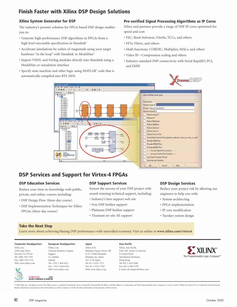
sretrauqdaeH etaroproC.cnI,xniliX
evirD cigoL 0012
42159 AC,esoJ naS
8777-955 )804(:leT
4117-955 )804(:xaF
moc.xnilix.www:beW
sretrauqdaeH naeporuE.dtL,xniliX
supmaC ssenisuB tsewytiC
,traggaS
nilbuD.oC
dnalerI
1130-464-1-353+:leT
4230-464-1-353+:xaF
moc.xnilix.www:beW
napaJ.K.K,xniliX
F81 rewoT erauqS ukujnihS
ukujnihS-ihsiN 1-22-6
oykoT,uk-ukujnihS
napaJ,8111-361
1177-1235-3-18:leT
5677-1235-3-18:xaF
pj.oc.xnilix.www:beW
cificaP aisAcificaP aisA,xniliX
yawetaG,6 rewoT,1021 tinU
daoR notnaC 9
,noolwoK,iustahsmisT
gnoK gnoH
0025-424-2-258:leT
9517-494-2-258:xaF
moc.xnilix@capaisa-ksa:liam-E
orciM dna,ezalBociP,PSDemertX,OItekcoR,4-xetriV;kramedart deretsiger a si eman xniliX ehT.devreser sthgir llA.cnI xniliX 5002 © es a si ynapmoC cigoL elbammargorP ehT dna;skramedart era ezalB lanoitanretnIfo kramedart a si CP rewoP.cnI xniliXfo kram ecivr
nwo riehtfo ytreporp eht era skramedart rehto llA.htob ro,seirtnuoc rehto ro,setatS detinU eht ni noitaroproC senihcaM ssenisuB .sre
ynapmoC cigoL elbammargorP ehT MS
PSD rof rotareneG metsyS xniliX
oitulos reimerp s’yrtsudni ehT selbane ngised PSD desab-AGPF rof n
:ot uoy
a morf sAGPF ni smhtirogla PSD ecnamrofrep-hgih etareneG•
knilumiS ni noitacificeps elbatucexe level hgih ®
tegrat ruoy gnisu edutingamfo sredro yb snoitalumis etareleccA•
miSledoM roknilumiS htiw”pool eht ni“ erawdrah ®
a gnisu knilumiS otni yltcerid seludom golireV dna LDHV tropmI•
ecafretni noitalumis-oc miSledoM
BALTAM gnisu cigol rehto dna enihcam etats yficepS• ® si taht edoc
LDH LTR otni delipmoc yllacitamotua
seroC PI sa smhtiroglA gnissecorP langiS deifirev-erProf dezimitpo seroc PI PSDfo egnar a edivorp srentrap dna xniliX
:tsoc dna deeps
srehto dna,sCCT,ibretiV,nomoloS-deeR:CEF•
srehto dna,sretliF,sTFF•
srehto dna,sCAM,reilpitluM,CIDROC:snoitcnuf htaM•
srehto dna gnilacs noisserpmoC—PI oediV•
,ICP,OIdipaR laireS htiw ytivitcennoc PSD dradnats-yrtsudnI•
FIME dna
snoituloS ngiseD PSD xniliX htiw retsaF hsiniF
sAGPF 4-xetriV rof troppuS dna secivreS PSDsecivreS noitacudE PSD
,cilbup htiw egdelwonk-ot-emit ruoy ecudeR
:gnidulcni sesruoc enilno dna,etavirp
)esruoc yad-eerht( wolF ngiseD PSD•
xniliX rof seuqinhceT noitatnemelpmI PSD•
)esruoc yad-eerht( sAGPF
secivreS troppuS PSD htiw tcejorp PSD ruoyfo sseccus eht erusnE
:gnidulcni,troppus lacinhcet gninniw-drawa
etis bew troppus tseb s’yrtsudnI•
troppus eniltoh PSD eerF•
troppus eniltoh PSD munitalP•
troppus EA etis-no muinatiT•
secivreS ngiseD PSDruo gniwolla yb ksir tcejorp ruoy ecudeR
:htiw uoy pleh ot sreenigne
gnitcetihcra metsyS•
noitatnemelpmi AGPF•
noitacifidom eroc PI•
ngised metsys yeknruT•
petS txeN eht ekaT ta enilno su tisiV.ymonoce dellavirnu htiw ecnamrofrep PSD gnizalb gniveihca tuoba erom nraeL 4xetriv/moc.xnilix.www
82 DSP magazine October 2005

Turbocharge yourDSP performance
Achieve high-definition, higher frame rates or multiple video streams
When complimenting a TI DSP, Xilinx XtremeDSP co-processing offers the performance,versatility, and economy for today’s high-end video and imaging applications.Whether it’s high-definition, motion estimation, video scaling, or any number ofcompute intensive functions, a Xilinx Virtex-4 or Spartan-3/3E FPGA can boostyour DSP performance. XtremeDSP co-processing delivers higher resolution,higher frame rate video processing than a standalone DSP processor, plus theability to handle multiple video streams.
Reduce power and cost per channel in wireless systems
For implementing custom wireless functions, such as multi-carrier crest factor reduction(CFR), digital pre-distortion (DPD), MIMO and other advanced antenna processing,our FPGAs lower your costs and power per channel. With up to 256 GMAC/s performance,you have the advantage of offloading compute intensive tasks from a TI DSP to aXilinx FPGA while increasing channel density in your wireless system.
Visit us at www.xilinx.com/dsp/coprocessing to learn more about the highest-performance DSP in the industry, and download your FREE evaluation copy ofXtremeDSP software.
www.xilinx.com/dsp/coprocessing
© 2005 Xilinx, Inc., All rights reserved. XILINX, the Xilinx logo, and other designated brands included herein are trademarks of Xilinx, Inc. All other trademarks are the property of their respective owners.
PN 0010886