điện tử tương tự,nguyễn vũ thắng,dhbkhcm
47
1. Structure of the Lesson Intro Class Class end Study Assessment Review 1. intro – Overview of the lesson 2. Learning objective – present learning objective of the lesson 3. Table of Content – structure of the topics and subtopics in the lesson 4. Lecture (75-90 minutes) – present the lecture in detailed topics that covers all the learning objectives of the lesson. - each topics should be divided into subtopics (5-15 min in length is recommended) - if a subtopic goes over 15 minutes divide the subtopic into series of subtopics. CuuDuongThanCong.com https://fb.com/tailieudientucntt
-
Upload
khangminh22 -
Category
Documents
-
view
0 -
download
0
Transcript of điện tử tương tự,nguyễn vũ thắng,dhbkhcm

1. Structure of the Lesson
Intro
Class
Class end
Study
Assessment
Review
1. intro – Overview of the lesson
2. Learning objective – present learning objective of the lesson
3. Table of Content – structure of the topics and subtopics in the
lesson
4. Lecture (75-90 minutes)
– present the lecture in detailed topics that covers all the
learning objectives of the lesson.
- each topics should be divided into subtopics
(5-15 min in length is recommended)
- if a subtopic goes over 15 minutes divide the subtopic into
series of subtopics.
CuuDuongThanCong.com https://fb.com/tailieudientucntt

Course Circuit theory and Laboratory
Lesson # Lesson 2
Title Bipolar Junction Transistor modelling
SME Dr. Nguyen Vu Thang
CuuDuongThanCong.com https://fb.com/tailieudientucntt

Intro
•The basic of electronic system is semiconductor device. The most famous and commonly used
active devices are BJTs (Bipolar Junction Transistors) and FET (Field Effect Transistor).
•BJT can be use as amplifier and logic switches.
•Pre-required knowledge: structure and operation of diode
CuuDuongThanCong.com https://fb.com/tailieudientucntt

Learning Objectives Table of Content
At the end of this chapter, the students shouldbe able to:
• Understand BJT modeling• Important parameters Zi, Zo, Av, Ai• The re Transistor Model• The Hybrid Equivalent Model
• Amplification in the AC Domain • BJT Transistor Modeling • The Important Parameters: Zi, Zo, Av, Ai • The re Transistor Model • The Hybrid Equivalent Model
CuuDuongThanCong.com https://fb.com/tailieudientucntt

Introduction1. The basic construction, appearance, and characteristics of the transistor were introduced in
lecture 2, the dc biasing of the device was then examined in detail in lecture 3. We now
begin to examine the small-signal ac response of the BJT amplifier by reviewing the models
most frequently used to represent the transistor in the sinusoidal ac domain.
2. One of our first concerns in the sinusoidal ac analysis of transistor networks is the
magnitude of the input signal. It will determine whether small-signal or large signal
techniques should be applied. There is no set dividing line between the two, but the
application and the magnitude of the variables of interest relative to the scales of the
device characteristics––will usually make it quite clear which method is appropriate. The
small-signal technique is introduced in this chapter, and large-signal applications are
examined in other course.
3. There are two models commonly used in the small-signal ac analysis of transistor networks:
the re model and the hybrid equivalent model. This chapter not only introduces both
models but defines the role of each and the relationship between the two.
CuuDuongThanCong.com https://fb.com/tailieudientucntt

Amplification in AC Domain
Perhaps the role of the dc supply can best be described by first considering the simple dc network of Fig. 7.1. The resulting direction of flow is indicated in the figure with a plot of the current i versus time. Let us now insert a control mechanism such as that shown in Fig. 7.2. The control mechanism is such that the application of a relatively small signal to the control mechanism can result in a much larger oscillation in the output circuit.CuuDuongThanCong.com https://fb.com/tailieudientucntt

BJT Transistor ModelingThe key to transistor small-signal analysis is the use of equivalent circuits (models)
1. A model is the combination of circuit elements, properly chosen, that best
approximates the actual behavior of a semiconductor device under specific
operating conditions.
Once the ac equivalent circuit has been determined, the graphical symbol of the device
can be replaced in the schematic by this circuit and the basic methods of ac circuit
analysis (mesh analysis, nodal analysis, and Thévenin’s theorem) can be applied to
determine the response of the circuit
There are two popular equivalent circuit to be substituted for the transistor: the hybrid
parameters and the re model
Hybrid parameters: used by manufacturer for a particular operating region on their
specification sheets but not accurate for a few operating condition
Re model: fails to account for the output impedance level of the device and the
feedback effect from output to input.
In an effort to demonstrate the effect that the ac equivalent circuit will have on the
analysis to follow
The dc levels were simply important for determining the proper Q-point of operation.
Once determined, the dc levels can be ignored in the ac analysis of the network.CuuDuongThanCong.com https://fb.com/tailieudientucntt

BJT Transistor Modeling
C
C1
C2 B
E
+
VCC
RC
_
R1
R2 RE CE
Rs
+
_
+
_
Vo
ViVsAC
CB
E
RC
R1
R2
Rs
AC
+
_
Vo+
_Vs
+
_
Vi
Figure 1. Transistor circuit under examination in this introductory discussion
Figure 2. The network of Figure 1 following removal of the dc supply and insertion of the short circuit equivalent for the capacitors.
CuuDuongThanCong.com https://fb.com/tailieudientucntt

BJT Transistor Modeling
Zi
AC
Transistor AC small
signal equivalent circuitC
B
ERC
R1 || R2
Rs
+
_
Vo+
_Vs
+
_
Vi
Ii Io
Zo
Figure 3. Circuit of Figure 2 redrawn for ac small signal analysis.
If we establish a common ground and rearrange the elements of Fig., R1 andR2 will be in parallel and RC will appear from collector to emitter as shown in FigSince the components of the transistor equivalent circuit appearing in Fig. 7.5employ familiar components such as resistors and independent controlled sources,
Let us identify the important quantities to be determined for the system. Since we know that the transistor is an amplifying device, we would expect some indication of how the output voltage Vo is related to the input voltage Vi—the voltage gain. Similar, we need to define current gain Ai = Io/Ii. The input impedance Zi and outputimpedance Zo will prove particularly important in the analysis
CuuDuongThanCong.com https://fb.com/tailieudientucntt

BJT Transistor Modeling
In summary, therefore, the ac equivalent of a network is obtained by:
1. Setting all dc sources to zero and replacing them by a short-circuit
equivalent
2. Replacing all capacitors by a short circuit equivalent
3. Removing all elements bypassed by the short-circuit equivalents
introduced by steps 1 and 2
4. Redrawing the network in a more convenient and logical form
CuuDuongThanCong.com https://fb.com/tailieudientucntt

BJT Transistor Modeling
Before investigating the equivalent circuits for BJTs in some detail, let us concentrate on those parameters of a two-port system that are of paramount importance from an analysis and design viewpoint. For the two-port (two pairs of terminals) system of Fig. 7.6, the input side (the side to which the signal is normally applied) is to the left
and the output side (where the load is connected) is to the right.
+
_
Vi
Ii Io
ZoZi
+
_
Vo
CuuDuongThanCong.com https://fb.com/tailieudientucntt

The Important Parameters: Zi, Zo, Av, Ai
Two-port
system
AC
Ii
Zi
Rsense+
_
Vi
+
_
Vs Two-port system AC
Io
Zo
+
_
Vo
+
_
VRsense
Rsense
For the input side, the input impedance Zi is defined by Ohm’s law as the following:
Note:
The input impedance of a BJT transistor amplifier is purely resistive
An ohmmeter cannot be used to measure the small-signal ac input impedance since the ohmmeter operates in the dc mode.
CuuDuongThanCong.com https://fb.com/tailieudientucntt

The Important Parameters: Zi, Zo, Av, Ai
The importance of the input impedance of a system can best be demonstrated by this example:
The signal source has an Zi = 600 ohm, and the system (possibly a transistor amplifier) has an input resistance of 1.2 k.
If the source were ideal (Rs =0), the full 10 mV would be applied to the system
But with a source impedance, the input voltage must be determined using the voltage divider rule
If Zi = 600 ohm, then Vi =5 mV or 50% of the available signal.
If Zi = 8.2 k, then Vi will be 93.2% of the applied signal
Zi should be as large as possible
CuuDuongThanCong.com https://fb.com/tailieudientucntt
The Important Parameters: Zi, Zo, Av, Ai
Two-port system AC
Io
Zo
+
_
Vo
+
_
VRsense
Rsense
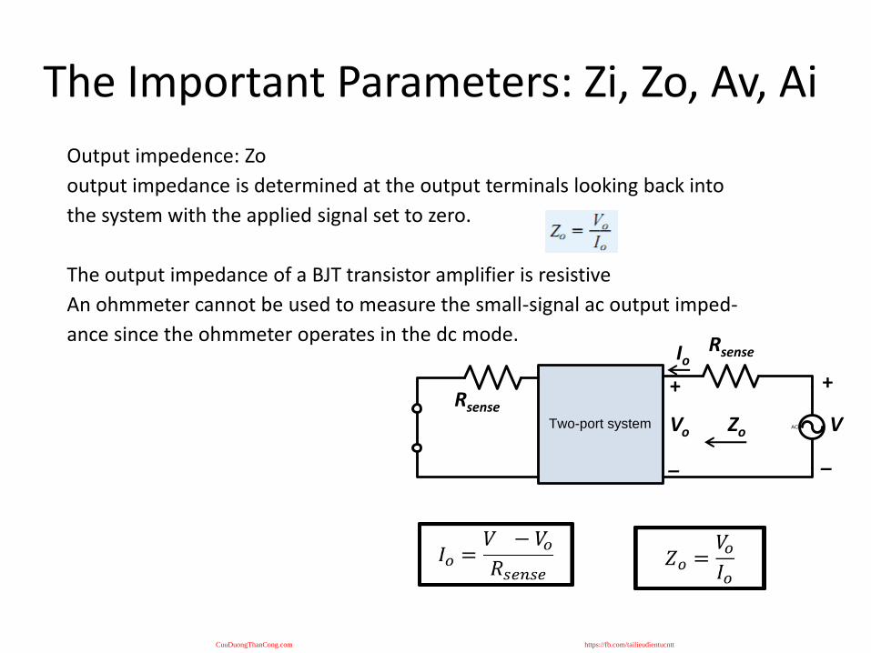
Output impedence: Zo
output impedance is determined at the output terminals looking back into
the system with the applied signal set to zero.
The output impedance of a BJT transistor amplifier is resistive
An ohmmeter cannot be used to measure the small-signal ac output imped-
ance since the ohmmeter operates in the dc mode.
CuuDuongThanCong.com https://fb.com/tailieudientucntt

The Important Parameters: Zi, Zo, Av, Ai
Zi
+
_
Vo
Rsense
+
_
Vs AC
One of the most important characteristics of an amplifier is the small-signal ac voltage gain as determined by
CuuDuongThanCong.com https://fb.com/tailieudientucntt

The Important Parameters: Zi, Zo, Av, Ai
For the BJT amplifier of Fig, determine:(a) Vi.(b) Ii.(c) Zi.(d) Avs.
CuuDuongThanCong.com https://fb.com/tailieudientucntt
The Important Parameters: Zi, Zo, Av, Ai
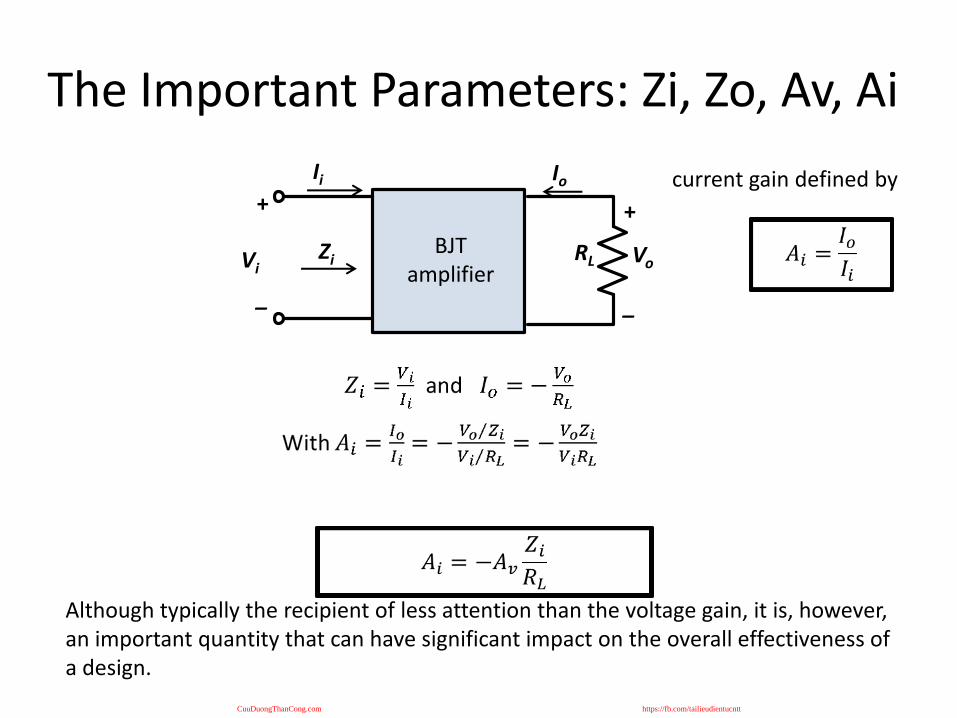
RL
+
_
Vi
Ii Io
Zi
+
_
VoBJT
amplifier
Although typically the recipient of less attention than the voltage gain, it is, however,an important quantity that can have significant impact on the overall effectiveness ofa design.
current gain defined by
CuuDuongThanCong.com https://fb.com/tailieudientucntt

The Important Parameters: Zi, Zo, Av, Ai
Zi
+
_
+
_
AC
CuuDuongThanCong.com https://fb.com/tailieudientucntt

The Important Parameters: Zi, Zo, Av, Ai
CuuDuongThanCong.com https://fb.com/tailieudientucntt
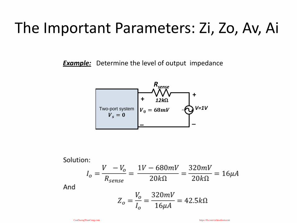
The Important Parameters: Zi, Zo, Av, Ai
Two-port system AC
+
_
+
_
V=1V
Rsense
Example: Determine the level of output impedance
CuuDuongThanCong.com https://fb.com/tailieudientucntt

The re Transistor Model
The re model employs a diode and controlled current source to duplicate the behavior of a transistor in the region of interest. Recall that a current-controlled current source is one where the parameters of the current source are controlled by a currentelsewhere in the network. In fact, in general:BJT transistor amplifiers are referred to as current-controlled devices.
CuuDuongThanCong.com https://fb.com/tailieudientucntt

The re Transistor Model
a common-base pnp transistor has been inserted within the two-port structure The re model for the transistor has been placed between the same four terminals. The model (equivalent circuit) is chosen in such a way as to approximate the behavior of the device it is replacing in the operating region of interestYou will recall from previous lecture that one junction of an operating transistor is forward-biased while the other is reverse-biased.The forward-biased base-to-emitter junction will behave much like a diode The diode equivalence between the same two terminals seems to be quite appropriate. For the output side, recall that Ic = alpha Ie. Therefore, The current source is established
CuuDuongThanCong.com https://fb.com/tailieudientucntt
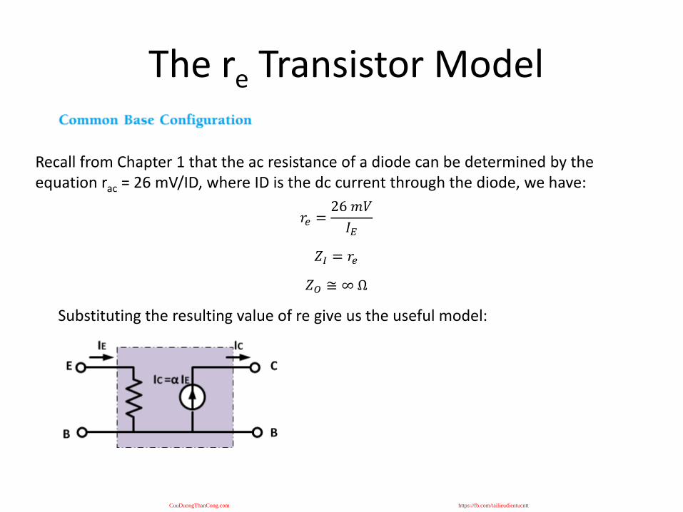
The re Transistor Model
Recall from Chapter 1 that the ac resistance of a diode can be determined by theequation rac = 26 mV/ID, where ID is the dc current through the diode, we have:
Substituting the resulting value of re give us the useful model:
CuuDuongThanCong.com https://fb.com/tailieudientucntt

The re Transistor Model
CuuDuongThanCong.com https://fb.com/tailieudientucntt

The re Transistor Model
CuuDuongThanCong.com https://fb.com/tailieudientucntt

The re Transistor Model
For the common-emitter configuration, the input terminals are the base and emitter terminals, but the output set is now the collector and emitter terminals Substituting the re equivalent circuit for the npn transistor will result in the configuration on the right
CuuDuongThanCong.com https://fb.com/tailieudientucntt
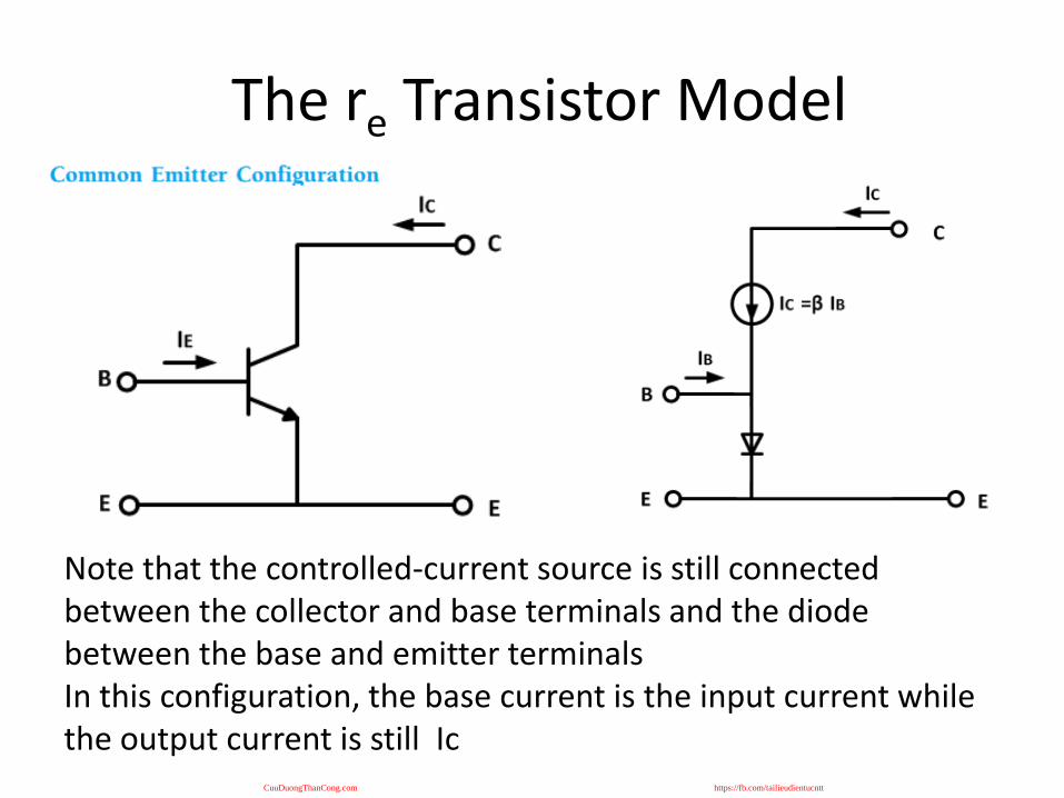
The re Transistor Model
Note that the controlled-current source is still connected between the collector and base terminals and the diode between the base and emitter terminalsIn this configuration, the base current is the input current while the output current is still Ic
CuuDuongThanCong.com https://fb.com/tailieudientucntt

The re Transistor Model
CuuDuongThanCong.com https://fb.com/tailieudientucntt

The re Transistor Model
CuuDuongThanCong.com https://fb.com/tailieudientucntt

The re Transistor Model For a common-base configuration with , , and an ac
signal of 2mV applied between the base and emitter terminals:
(a) Determine the input impedance
(b) Calculate the voltage gain if a load of 0.56 kΩ is connected
to the output terminals.
(c) Find the output impedance and current gain.
E C
B B
IE IC
=α IC IE
re
CuuDuongThanCong.com https://fb.com/tailieudientucntt

The re Transistor Model Solution:
CuuDuongThanCong.com https://fb.com/tailieudientucntt

The re Transistor Model Given and for a common-emitter configuration
with determine:
(a)
(b) if a load of 2 kΩ is applied
(c) with the 2 kΩ load
CB
Ib
β Ib
EE
roreβ
CuuDuongThanCong.com https://fb.com/tailieudientucntt

The re Transistor Model
CB
Ib
β Ib
EE
roreβ
Solution
CuuDuongThanCong.com https://fb.com/tailieudientucntt

The Hybrid Equivalent ModelThe re model for a transistor is sensitive to the dc level of operation of the amplifier. The result is an input resistance that will vary with the dc operating point. For the hybrid equivalent model, the parameters are defined at an operating point that may or may not reflect the actual operating conditions of the amplifier. This is due to the specification sheets cannot provide parameters for an equivalent circuit at every possible operating point. They must choose operating conditions that they believe reflect the general characteristics of the device. One obvious advantage of the specification sheet listing is the immediate knowledge of typical levels for the parameters of the device as compared to other transistors.
CuuDuongThanCong.com https://fb.com/tailieudientucntt

The Hybrid Equivalent Model
Min Max
Input impedance ( )
0.5 7.5 kΩ
Voltage feedback ratio ( )
0.1 8.0 X
Small-signal current gain ( )
20 250 _
Output admittance ( )
1.0 30 1 µS
The quantities hie, hre, hfe, and hoe of table below are called the hybrid parameters
CuuDuongThanCong.com https://fb.com/tailieudientucntt

The Hybrid Equivalent Model1
+
_Vi
Ii Io
+
_Vo
1’
2
2’
description of the hybrid equivalent model will begin with the general two-port system of Fig aboveThe 2 equations give relation of the 4 variablesThe parameters relating the four variables are called h-parameters from the word “hybrid.”
short-circuit input-impedance parameter
ohms
open-circuit reverse transfer voltage ratio parameter
unitless
CuuDuongThanCong.com https://fb.com/tailieudientucntt

The Hybrid Equivalent Model
Ii Io+
_
VoACDC
+
_
Vi
+
_
hi
ho
AC
Ii
+
_
+
_
Hybrid input equivalent circuit
DC
Io+
_
Vo
Hybrid output equivalent circuit
short-circuit forward transfer current ratio parameter
siemens
unitless
open-circuit out-put admittance parameter
h11 → input resistance → hih12 → reverse transfer voltage ratio → hrh21 → forward transfer current ratio → hfh22 → output conductance → ho
CuuDuongThanCong.com https://fb.com/tailieudientucntt

The Hybrid Equivalent Model
IE
IB
C
B
E
+
VBE_
+
_
VCE
AC
+
__
+
B
CE AC
+
__
+
Common-emitter configuration: (a) graphical symbol; (b) hybrid equivalent circuit
Common-base configuration: (a) graphical symbol; (b) hybrid equivalent circuit
CuuDuongThanCong.com https://fb.com/tailieudientucntt

The Hybrid Equivalent Model
+
_
Vi
Ii Io
+
_
Vo
+
_
Vi
Ii Io
+
_
Vo
cb
ee ee
b c
b
e c
b
ce
b bCuuDuongThanCong.com https://fb.com/tailieudientucntt

The Hybrid Equivalent Model
cb
ee
ce
b b
Common-emitter hybrid equivalent circuit
Example: given IE = 2.5 mA, hfe = 140, hoe = 20 μS, and hob = 0.5 μS, determine:The common-emitter hybrid equivalent circuit.The common-base re model.
CuuDuongThanCong.com https://fb.com/tailieudientucntt

The Hybrid Equivalent Model
CuuDuongThanCong.com https://fb.com/tailieudientucntt

Quiz 1
a) For the configuration of fig, determine Zi if Vs = 40 mV, Rsense = 0.5 kΩ, and Ii = 20µA.
b) Using the results of part a), determine Vi if the applied source is changed to 12 mV with an internal resistance of 0.4 kΩ
-Solution:
CuuDuongThanCong.com https://fb.com/tailieudientucntt

Quiz 2
CuuDuongThanCong.com https://fb.com/tailieudientucntt

Quiz 3
CuuDuongThanCong.com https://fb.com/tailieudientucntt
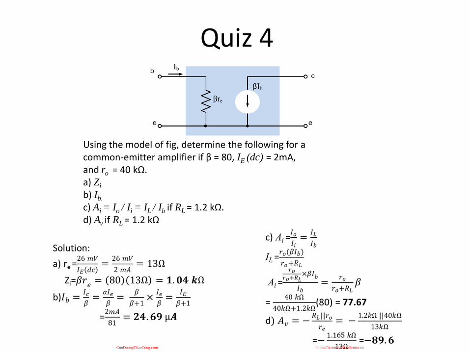
Quiz 4
Using the model of fig, determine the following for a common-emitter amplifier if β = 80, IE (dc) = 2mA, and ro = 40 kΩ.a) Zi
b) Ib.
c) Ai = Io / Ii = IL / Ib if RL = 1.2 kΩ.d) Av if RL = 1.2 kΩ
CuuDuongThanCong.com https://fb.com/tailieudientucntt

Quiz 5
CuuDuongThanCong.com https://fb.com/tailieudientucntt

Review
Summary: this chapter provide Operating point, Bias circuits, Transistor switching network, Bias Stabilization. Main Bias circuits are: Fixed – bias Circuit , Emitter stabilized bias Circuit, Voltage - divider bias Circuit
CuuDuongThanCong.com https://fb.com/tailieudientucntt