CM4540 English 1 - Cover.indd - YoReparo
67
Mini Hi-Fi System SERVICE MANUAL MODEL: CM4540 (CM4540, CMS4540F/W) CAUTION BEFORE SERVICING THE UNIT, READ THE “SAFETY PRECAUTIONS” IN THIS MANUAL. MODEL: CM4540 (CM4540, CMS4540F/W) SERVICE MANUAL 4 1 0 2 , JULY 76615081 N F A : O N / P Website http://biz.lgservice.com Internal Use Only
-
Upload
khangminh22 -
Category
Documents
-
view
0 -
download
0
Transcript of CM4540 English 1 - Cover.indd - YoReparo

Mini Hi-Fi SystemSERVICE MANUAL
MODEL: CM4540 (CM4540, CMS4540F/W)CAUTIONBEFORE SERVICING THE UNIT, READ THE “SAFETY PRECAUTIONS”IN THIS MANUAL.
MO
DE
L: C
M4540 (C
M4540, C
MS
4540F/W
)S
ER
VIC
E M
AN
UA
L
4102,JULY76615081NFA:ON/P
Website http://biz.lgservice.comInternal Use Only

CONTENTS
SECTION 1 ........GENERAL
SECTION 2 ........CABINET & MAIN CHASSIS
SECTION 3 ........ELECTRICAL
SECTION 4 ........REPLACEMENT PARTS LIST
1-1

SECTION 1
SUMMARY
CONTENTS
SERVICING PRECAUTIONS ................................................................................................................... 1-3
ESD PRECAUTIONS .................................................................................................................................. 1-5
HIDDEN KEY MODE................................................................................................................................... 1-6
SERVICE INFORMATION FOR EEPROM .......................................................................................... 1-7
PROGRAM DOWNLOAD & UPDATE GUIDE ................................................................................... 1-81. MCS PROGRAM ....................................................................................................................................... 1-82. EQ PROGRAM ......................................................................................................................................... 1-9
SPECIFICATIONS ..................................................................................................................................... 1-10
1-2

NOTES REGARDING HANDLING OF THE PICK-UP1. Notes for transport and storage
1) The pick-up should always be left in its conductive bag until immediately prior to use.2) The pick-up should never be subjected to external pressure or impact.
2. Repair notes1) The pick-up incorporates a strong magnet, and so should never be brought close to magnetic materials.2) The pick-up should always be handled correctly and carefully, taking care to avoid external pressure and
impact. If it is subjected to strong pressure or impact, the result may be an operational malfunction and/or damage to the printed-circuit board.
3) Each and every pick-up is already individually adjusted to a high degree of precision, and for that reason the adjustment point and installation screws should absolutely never be touched.
4) Laser beams may damage the eyes!Absolutely never permit laser beams to enter the eyes!Also NEVER switch ON the power to the laser output part (lens, etc.) of the pick-up if it is damaged.
5) Cleaning the lens surfaceIf there is dust on the lens surface, the dust should be cleaned away by using an air bush (such as used for camera lens). The lens is held by a delicate spring. When cleaning the lens surface, therefore, a cotton swab should be used, taking care not to distort lens.
6) Never attempt to disassemble the pick-up.Spring has excess pressure. If the lens is extremely dirty, apply isopropyl alcohol to the cotton swab. (Do not use any other liquid cleaners, because they will damage the lens.) Take care not to use too much of this alcohol on the swab, and do not allow the alcohol to get inside the pick-up.
Storage in conductive bag Drop impact
NEVER look directly at the laser beam, and don’t allow contact with fingers or other exposed skin.
Magnet
How to hold the pick-up
Conductive Sheet
Cotton swab
Pressure
Pressure
1-3
SERVICING PRECAUTIONS

NOTES REGARDING COMPACT DISC PLAYER REPAIRS1. Preparations1) Compact disc players incorporate a great many ICs as well as the pick-up (laser diode). These components
are sensitive to, and easily affected by, static electricity. If such static electricity is high voltage, components can be damaged, and for that reason components should be handled with care.
2) The pick-up is composed of many optical components and other high-precision components. Care must be taken, therefore, to avoid repair or storage where the temperature or humidity is high, where strong magnet-ism is present, or where there is excessive dust.
2. Notes for repair1) Before replacing a component part, first disconnect the power supply lead wire from the unit2) All equipment, measuring instruments and tools must be grounded.3) The workbench should be covered with a conductive sheet and grounded.
When removing the laser pick-up from its conductive bag, do not place the pick-up on the bag. (This is because there is the possibility of damage by static electricity.)
4) To prevent AC leakage, the metal part of the soldering iron should be grounded.5) Workers should be grounded by an armband (1 MΩ)6) Care should be taken not to permit the laser pick-up to come in contact with clothing, in order to prevent stat-
ic electricity changes in the clothing to escape from the armband.7) The laser beam from the pick-up should NEVER be directly facing the eyes or bare skin.
Resistor(1 MΩ) Conductive
Sheet
Resistor(1 MΩ)
Armband
1-4

Electrostatically Sensitive Devices (ESD)Some semiconductor (solid state) devices can be damaged easily by static electricity. Such componentscommonly are called Electrostatically Sensitive Devices (ESD). Examples of typical ESD devices are integratedcircuits and some field-effect transistors and semiconductor chip components. The following techniques shouldbe used to help reduce the incidence of component damage caused by static electricity.
1. Immediately before handling any semiconductor component or semiconductor-equipped assembly, drain offany electrostatic charge on your body by touching a known earth ground. Alternatively, obtain and wear acommercially available discharging wrist strap device, which should be removed for potential shock reasonsprior to applying power to the unit under test.
2. After removing an electrical assembly equipped with ESD devices, place the assembly on a conductive surface such as aluminum foil, to prevent electrostatic charge buildup or exposure of the assembly.
3. Use only a grounded-tip soldering iron to solder or unsolder ESD devices.
4. Use only an anti-static solder removal device. Some solder removal devices not classified as "anti-static" can generate electrical charges sufficient to damage ESD devices.
5. Do not use freon-propelled chemicals. These can generate electrical charges sufficient to damage ESDdevices.
6. Do not remove a replacement ESD device from its protective package until immediately before you areready to install it. (Most replacement ESD devices are packaged with leads electrically shorted together byconductive foam, aluminum foil or comparable conductive materials).
7. Immediately before removing the protective material from the leads of a replacement ESD device, touch theprotective material to the chassis or circuit assembly into which the device will by installed.
CAUTION : BE SURE NO POWER IS APPLIED TO THE CHASSIS OR CIRCUIT, AND OBSERVE ALL OTHER SAFETY PRECAUTIONS.
8. Minimize bodily motions when handing unpackaged replacement ESD devices. (Otherwise harmless motionsuch as the brushing together of your clothes fabric or the lifting of your foot from a carpeted floor can generate static electricity sufficient to damage an ESD device).
CAUTION. GRAPHIC SYMBOLS
THE LIGHTNING FLASH WITH APROWHEAD SYMBOL. WITHIN AN EQUILATERAL TRIANGLE, IS INTENDED TO ALERT THE SERVICE PERSONNEL TO THE PRESENCE OF UNINSULATED “DANGEROUS VOLTAGE” THAT MAY BE OF SUFFICIENT MAGNITUDE TO CONSTITUTE A RISK OF ELECTRIC SHOCK.
THE EXCLAMATION POINT WITHIN AN EQUILATERAL TRIANGLE IS INTENDED TO ALERT THESERVICE PERSONNEL TO THE PRESENCE OF IMPORTANT SAFETY INFORMATION IN SERVICELITERATURE.
1-5
ESD PRECAUTIONS

1-6
Push both Front key and RCU key to activate it for 5 seconds.
1. Disc Lock On/Off (CD Function Only Active) Front Key : STOP RCU Key : STOP
2. Check Version and Option code Front Key : STOP RCU Key : PLAY/PAUSE You can change [Audio MCU Version <-> CD Controller Version <-> EEPROM Option] by SKIP+/-.
3. Clear EEPROM Front Key : STOP RCU Key : SKIP-
4. Edit EEPROM Front Key : STOP RCU Key : SKIP+ You can change the digit of option by SKIP+/-. You can edit 0~f by REPEAT or PLAY/PAUSE key.
5. Bluetooth DUT Front Key : STOP RCU Key : PROGRAM Bluetooth model only
6. Power Disc Lock On/Off (CD Function Only Active) Front Key : STOP RCU Key : EQ
7. Amp Clip On/Off Front Key : STOP RCU Key : Mute
Amp Clip Mode Change (Amp Clip On --> Amp Clip Off --> Level Down display).
HIDDEN KEY MODE

POWER ON
FLD no disc status or AUX status.
Remote control ‘Fwd skip’ + Front ‘STOP’ push same timing during 5 seconds.
FLD ‘OP-0….
Move to appropriate position and make changes with remote control
‘skip, mode, play’ key.
Press ENTER key
FLD ‘write ok’
Remote control ‘Fwd skip’ +Front ‘STOP’ push same timing
FLD ‘E2P CLR’
Completed
NAME
OPT0OPT1OPT2OPT3OPT4OPT5OPT6OPT7OPT8OPT9
DETECT NEW EEPROM(OPTION EDIT SCREEN)
HEX
05000002000181062000
1-7
SERVICE INFORMATION FOR EEPROM

1. MCS PROGRAM
Download program file name must be - HG440_CM4740_DATE.bin : CM4740 4M Flash- HG420_CM4740_DATE.bin : CM4740 2M Flash- HG440_CM464P_DATE.bin : CM4640P (With Ipod)
If security program (Water Wall) is activated on your PC, you must save the file to the USB storagedevice and disable the security software, then download the file to your set.
Caution: When downloading the file, you should neither unplug the USB device, change to the otherfunction, nor power off the device. USB device must be unplugged when the downloadingprocess is completed.
ON VFD DISPLAY SCREEN
NO USB
↓ ← Insert USB device at USB function.
SEARCH
↓FIRMWARE
↓FINISH
↓POWER OFF MANUALLY ← When completed, remove USB device.
1-8
PROGRAM DOWNLOAD & UPDATE GUIDE

2. EQ PROGRAM
Download program file name must be EQ_PRG_CM4740_***.BIN If security program (Water Wall) is activated on your PC, you must save the file to the USB storagedevice and disable the security software, then download the file to your set.
Caution: When downloading the file, you should neither unplug the USB device, change to the otherfunction, nor power off the device. USB device must be unplugged when the downloadingprocess is completed.
ON VFD DISPLAY SCREEN
NO USB
↓ ← Insert USB device at USB function.
SEARCH
↓EQ UP
↓FINISH
↓POWER OFF AUTOMATICALLY ← When completed, remove USB device.
1-9

SPECIFICATIONS
1-10
• GENERAL.lebal niam eht ot refeR stnemeriuqer rewoP.lebal niam eht ot refeR noitpmusnoc rewoP
Dimensions (W x H x D) 206 x 308 x 284 mmNet Weight (Approx.) 3.0 kgOperating temperature 5 °C to 35 °C (41 °F to 95 °F)
% 09 ot % 5 ytidimuh gnitarepOBus Power Supply (USB) 5 V 500 mA
• INPUTS 57 ,)Bd 0 ,zHk 1( smrV 0.2 NI XUA Ω, RCA jack (L, R) x 1
)kcaj oerets mm 5.3( smrV 2.1 NI TROP
• TUNERzHM 00.801 ot 05.78 ro zHM 0.801 ot 5.78 egnaR gninuT MF
zHk 017 1 ot 225 ro zHk 017 1 ot 025 ,zHk 026 1 ot 225 e (Optional)gnaR gninuT MA
• AMPLIFIER 3( W 002 + W 002 edom oeretS Ω at 1 kHz, THD 20 %)
Surround mode 3( W 002 + W 002 tnorF Ω at 1 kHz, THD 20 %)
3( W 002 refoowbuS Ω at 60 Hz, THD 20 %)
• CDFrequency Response 100 to 20 000 Hz
Bd 57 oitar esion-ot-langiSBd 57 egnar cimanyD
• FRONT SPEAKERF0454SMC ledoM
rekaepS 2 yaW 2 epyT 3 ecnadepmI Ω
W 002 rewoP tupnI detaRW 004 rewop tupnI .xaM
Net Dimensions (W x H x D) 266 x 306 x 263 mmgk 1.3 thgieW teN
• SUBWOOFER SPEAKERW0454SMC ledoM
rekaepS 1 yaW 1 epyT 3 ecnadepmI Ω
W 002 rewoP tupnI detaRW 004 rewop tupnI .xaM
Net Dimensions (W x H x D) 266 x 306 x 232 mmgk 7.4 thgieW teN
Design and specifications are subject to change without notice.

SECTION 2
CABINET & MAIN CHASSIS
CONTENTS
EXPLODED VIEWS ..................................................................................................................................... 2-31. CABINET AND MAIN FRAME SECTION (CM4540) ................................................................................ 2-32. MECHANISM DECK SECTION (DP17TM3) ............................................................................................ 2-53. PACKING ACCESSORY SECTION ......................................................................................................... 2-74. SPEAKER SECTION ................................................................................................................................ 2-8
2-1

2-2
MEMO

EXPLODED VIEWS1. CABINET AND MAIN FRAME SECTION (CM4540)
F 300
FRONT
SMPS
MAIN
E
B
A
D
DC
C
B
F
A
E
H
H
260L
260R
464
464
A47
264
463
463
269
262460
464
464
263255
255
464
464
A43464
464A46
464
265
266
A44
266
464
261
252
259
464
464
A42
251253
CABLE1
NOTES) THE EXCLAMATION POINT WITHIN AN EQUILATERAL TRIANGLE IS INTENDED TO ALERT THE SERVICE PERSONNEL TO THE PRESENCE OF IMPORTANT SAFETY INFORMATION IN SERVICELITERATURE.

2. MECHANISM DECK SECTION (DP17TM3)
1026
1439
A0011002
1005 1001
10491437
1437
1024
1024
1030
1024
1043
1045
A005
A006
10161013 1015
1020
1024
1003
1439
1018
1019
1011
1012
1437
1004

900 Remote Control
808 Battery
825 FM Wire Antenna
802 Box
801 Instruction Ass'y
804 Bag
803 Packing
803 Packing
3. PACKING ACCESSORY SECTION

A60
4. SPEAKER SECTION 4-1. FRONT SPEAKER (CMS4540F)

A90
4-2. SUBWOOFER SPEAKER (CMS4540W)

2-10
MEMO
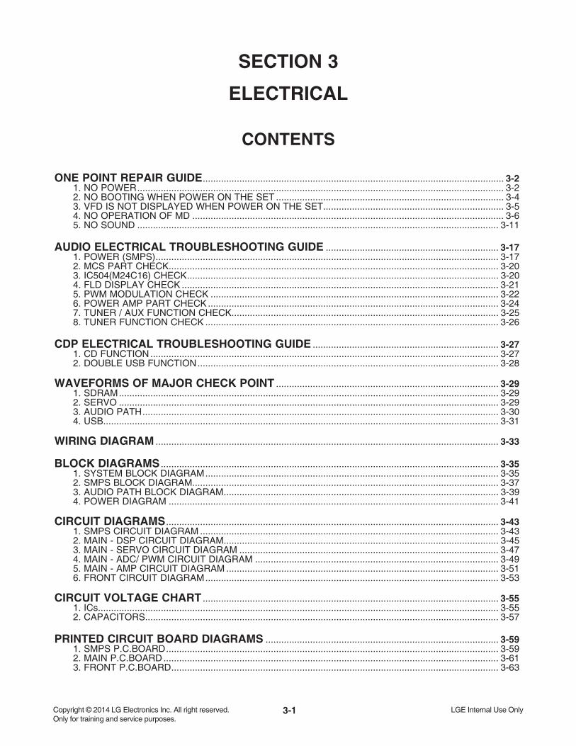
SECTION 3
ELECTRICAL
CONTENTS
ONE POINT REPAIR GUIDE ................................................................................................................... 3-21. NO POWER ............................................................................................................................................ 3-22. NO BOOTING WHEN POWER ON THE SET ....................................................................................... 3-43. VFD IS NOT DISPLAYED WHEN POWER ON THE SET ..................................................................... 3-54. NO OPERATION OF MD ....................................................................................................................... 3-65. NO SOUND .......................................................................................................................................... 3-11
AUDIO ELECTRICAL TROUBLESHOOTING GUIDE .................................................................. 3-171. POWER (SMPS) ................................................................................................................................... 3-172. MCS PART CHECK.............................................................................................................................. 3-203. IC504(M24C16) CHECK ....................................................................................................................... 3-204. FLD DISPLAY CHECK ......................................................................................................................... 3-215. PWM MODULATION CHECK .............................................................................................................. 3-226. POWER AMP PART CHECK ............................................................................................................... 3-247. TUNER / AUX FUNCTION CHECK ...................................................................................................... 3-258. TUNER FUNCTION CHECK ................................................................................................................ 3-26
CDP ELECTRICAL TROUBLESHOOTING GUIDE ....................................................................... 3-271. CD FUNCTION ..................................................................................................................................... 3-272. DOUBLE USB FUNCTION ................................................................................................................... 3-28
WAVEFORMS OF MAJOR CHECK POINT ..................................................................................... 3-291. SDRAM ................................................................................................................................................. 3-292. SERVO ................................................................................................................................................. 3-293. AUDIO PATH ........................................................................................................................................ 3-304. USB....................................................................................................................................................... 3-31
WIRING DIAGRAM ................................................................................................................................... 3-33
BLOCK DIAGRAMS ................................................................................................................................. 3-351. SYSTEM BLOCK DIAGRAM ................................................................................................................ 3-352. SMPS BLOCK DIAGRAM..................................................................................................................... 3-373. AUDIO PATH BLOCK DIAGRAM ......................................................................................................... 3-394. POWER DIAGRAM .............................................................................................................................. 3-41
CIRCUIT DIAGRAMS ............................................................................................................................... 3-431. SMPS CIRCUIT DIAGRAM .................................................................................................................. 3-432. MAIN - DSP CIRCUIT DIAGRAM ......................................................................................................... 3-453. MAIN - SERVO CIRCUIT DIAGRAM ................................................................................................... 3-474. MAIN - ADC/ PWM CIRCUIT DIAGRAM ............................................................................................. 3-495. MAIN - AMP CIRCUIT DIAGRAM ........................................................................................................ 3-516. FRONT CIRCUIT DIAGRAM ................................................................................................................ 3-53
CIRCUIT VOLTAGE CHART ................................................................................................................. 3-551. ICs......................................................................................................................................................... 3-552. CAPACITORS....................................................................................................................................... 3-57
PRINTED CIRCUIT BOARD DIAGRAMS ......................................................................................... 3-591. SMPS P.C.BOARD ............................................................................................................................... 3-592. MAIN P.C.BOARD ................................................................................................................................ 3-613. FRONT P.C.BOARD ............................................................................................................................. 3-63
3-1

3-2
ONE POINT REPAIR GUIDE
1. NO POWERIf the unit doesn’t work by no power problem, repair the set according to the following guide.
1-1. FUSE & BRIDGE DIODE1-1-1. SolutionPlease check and replace F901, BD901, TH901 or TH903 on SMPS board.
1-1-2. How to troubleshoot (Countermeasure)1) Check if the fuse F901 is open or short-circuit.2) Check if the bridge diode BD901 is short-circuit by over current with a digital multi meter.3) Check if the NTC thermistor TH901 or TH903 is normal or open.
1-1-3. Service hint (Any picture / Remark)
< F901 > If F901 is not short-circuit,
replace it with a same specifi cations one.
< TH901 > If TH901 is open,
replace it with a new one.
< BD901 > If BD901 is short-circuit,
replace it with a new one.

3-3
ONE POINT REPAIR GUIDE
NO POWERIf the unit doesn’t work by no power problem, repair the set according to the following guide.
1-2. D9511-2-1. SolutionPlease check and replace D951 on SMPS board.
1-2-2. How to troubleshoot (Countermeasure)1) Check the anode-cathod voltage of D951 with a digital multi-meter, it is normally 0.2 ~ 0.3 V. If it doesn’t have any voltage, it’s destroyed. Replace it with a new one.
1-2-3. Service hint (Any picture / Remark)
< SMPS schematic diagram >

3-4
ONE POINT REPAIR GUIDE
2. NO BOOTING WHEN POWER ON THE SETThe set doesn’t work when press the power button on the front board or the remote control.
2-1. FLASH MEMORY2-1-1. SolutionPlease check and replace IC503 on MAIN board.
2-1-2. How to troubleshoot (Countermeasure)1) Check 5.6 V to CN501 in standby mode. If there is no 5.6 V, check the SMPS.2) Check 12 V, F+, F- and PVDD when power on the set. - If the set doesn’t work regardless of what the KEY1 changes high to low while pressing the power button. X500 and X501 work normally but, if you can not power on the set, replace IC501 with a new one on the MAIN board.
2-1-3. Service hint (Any picture / Remark)
KEY1(R542)
IC501
PWR_CTRL(R53D)
< Signal check point >

3-5
ONE POINT REPAIR GUIDE
3. VFD IS NOT DISPLAYED WHEN POWER ON THE SETWhen power on the set, any icons or characters on VFD are not displayed.
3-1. VFD3-1-1. SolutionPlease check and replace DIG302 on FRONT board.
3-1-2. How to troubleshoot (Countermeasure)1) Check if VKK, FL+ and FL- are output from SMPS to VFD via the MAIN board.2) Check if IC501 outputs VFD_D0, VFD_CLK and VFD_STB to the FRONT board.3) Check the GR signal(pulse signal) of IC408 on the FRONT board. Check the SG signal(pulse signal) of IC408 on the FRONT board. If the GR and SG signal isn’t output, replace IC408 with a new one. If the GR and SG signal is output, replace DIG302 with a new one.
3-1-3. Service hint (Any picture / Remark)
GR signal
SG signal
< Waveform of GR and SG signal >
GR SIGNAL ABOUT 30V
SG SIGNAL ABOUT 30V
Click the picture, and then drag to enlarge it.
Check the waveform on details.

3-6
ONE POINT REPAIR GUIDE
4. NO OPERATION OF MDWhen no sound output in the CD function, you can not listen to music reading data from a CD disc if the servo motors in MD don’t work. This step is for checking the SPINDLE MOTOR among them.
4-1. SPINDLE MOTOR4-1-1. SolutionPlease check and replace IC407, IC408 on MAIN board.
4-1-2. How to troubleshoot (Countermeasure)1) Check the SPDO signal from pin24 of IC407. If no signal, check 3.3 V(RF) and X400.2) Check the SPIN- & SPIN+ from IC408 to CN405 for driving SPINDLE motor. It is about 3.6 Vp-p. If no signal, check +1.8 V and +5 V for IC408.3) Check if the FFC cable is solidly connected between CN405 and MD.4) Check the MD. If the spindle motor is sort-circuit or has any trouble, it can not rotate CD discs. Please check the function after changing another MD.
4-1-3. Service hint (Any picture / Remark)
About 3.6Vpp
Sp+Pin17 to CN405
Sp-Pin18 to CN405
< Waveform of SP- & SP+ for driving SPINDLE motor >
< Signal check point >

3-7
ONE POINT REPAIR GUIDE
NO OPERATION OF MDWhen no sound output in the CD function, you can not listen to music reading data from a CD disc if the servo motors in MD don’t work. This step is for checking the SLED MOTOR among them.
4-2. SLED MOTOR4-2-1. SolutionPlease check and replace IC407, IC408 on MAIN board.
4-2-2. How to troubleshoot (Countermeasure)1) Check the SLDO signal from Pin23 of IC407. If no signal, check 3.3 V(RF) and X400.2) Check the SLED+ & SLED- from IC408 to CN405 for driving SPINDLE motor. It is about 2.9 Vp-p. If no signal, check +1.8 V and +5 V for IC408.3) Check if the FFC cable is solidly connected between CN405 and MD.4) Check the MD. If the sled motor is sort-circuit or has any trouble, it can not move the pickup module. Please check the function after changing another MD.
4-2-3. Service hint (Any picture / Remark)
SL- TO CN405
SL+ TO CN405
SLED+Pin11 to CN405
SLED-Pin12 to CN405
< Waveform of SLED- & SLED+ for driving SLED motor >
< Signal check point >

3-8
ONE POINT REPAIR GUIDE
NO OPERATION OF MDWhen no sound output in the CD function, you can not listen to music reading data from a CD disc if the servo motors in MD don’t work. This step is for checking the TRAY OPEN / CLOSE MOTOR among them.
4-3. TRAY OPEN / CLOSE MOTOR4-3-1. SolutionPlease check and replace IC407, IC408 on MAIN board.
4-3-2. How to troubleshoot (Countermeasure)1) Check MOT_OPEN & MOT_CLOSE signals from Pin K4, L4 of IC501 to IC408. If no signal, check +1.8 V & + 5 V to IC408.2) Check LOAD± from IC408 to CN405 for driving the tray open / close motor. It is about 3.85 Vp-p. If no signal, check +5 V to IC408. If it has any trouble, replace it with a new one.3) Check if the FFC cable is solidly connected between CN405 and MD.4) Check the MD. If the tray motor is sort-circuit or has any trouble, it can not open or close the tray. Please check the function after changing another MD.
4-3-3. Service hint (Any picture / Remark)
LO- TO CN405LO+ TO CN405
MOT_OPENCLOSE
MOT_OPENPin7 to CN405
MOT_CLOSEPin6 to CN405
LOAD+Pin9 to CN405
LOAD-Pin10 to CN405
< Waveform for driving TRAY open / close motor >
< Signal check point >

3-9
ONE POINT REPAIR GUIDE
NO OPERATION OF MD When no sound output in the CD function, you can not listen to music reading data from a CD disc if the pickup module in MD doesn’t work. This step is for checking the LASER TRACKING ACTUATOR.
4-4. LASER TRACKING ACTUATOR4-4-1. SolutionPlease check and replace IC407, IC408 on MAIN board.
4-4-2. How to troubleshoot (Countermeasure)The tracking actuator makes the laser beam be positioned in the center of a track on CD disc.1) Check the TRD signal from Pin22 of IC407. If no signal, check 3.3 V(RF) and X400.2) Check TR- & TR+ from IC408 to CN408 for driving the tracking actuator. If no signal, check +1.8 V and +5 V for IC408.3) Check if the FFC cable is solidly connected between CN405 and MD.4) Check the MD. If the pickup module has any trouble, it can not move the laser beam on the left or right side. Please check the function after changing another MD.
4-4-3. Service hint (Any picture / Remark)
TR+Pin16 to CN405
TR-Pin15 to CN405
< Waveform of TR± for driving TRACKING actuator >
< Signal check point >
3-10
ONE POINT REPAIR GUIDE
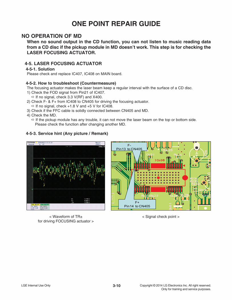
NO OPERATION OF MD When no sound output in the CD function, you can not listen to music reading data from a CD disc if the pickup module in MD doesn’t work. This step is for checking the LASER FOCUSING ACTUATOR.
4-5. LASER FOCUSING ACTUATOR4-5-1. SolutionPlease check and replace IC407, IC408 on MAIN board.
4-5-2. How to troubleshoot (Countermeasure)The focusing actuator makes the laser beam keep a regular interval with the surface of a CD disc.1) Check the FOD signal from Pin21 of IC407. If no signal, check 3.3 V(RF) and X400.2) Check F- & F+ from IC408 to CN405 for driving the focusing actuator. If no signal, check +1.8 V and +5 V for IC408.3) Check if the FFC cable is solidly connected between CN405 and MD.4) Check the MD. If the pickup module has any trouble, it can not move the laser beam on the top or bottom side. Please check the function after changing another MD.
4-5-3. Service hint (Any picture / Remark)
F+Pin14 to CN405
F-Pin13 to CN405
< Waveform of TR± for driving FOCUSING actuator >
< Signal check point >

3-11
ONE POINT REPAIR GUIDE
5. NO SOUNDThere is no sound output in the CD FUNCTION, repair the set according to the follow-ing guide.
5-1. IN THE CD FUNCTION5-1-1. SolutionPlease check and replace IC501, IC601 on MAIN board.
5-1-2. How to troubleshoot (Countermeasure)1) Check CD_BCLK, CD_LRCK, & CD_DOUTA signals from IC407 to IC501. If no signal, check if the RF & servo signals from MD is entered to IC407. Refer to the “No operation of MD” guide on Item 4.2) Check the following I2S signal flow. < I2S audio signal Interface > - DAC_BCK : IC501_Pin E1 --> IC601_Pin23 - DAC_LRCK : IC501_Pin D1 --> IC601_Pin22 (44.1 kHz) - DAC_DATA : IC501_Pin E2 --> IC601_Pin24 - DAC_MCLK : IC501_Pin D2 --> IC401_Pin44 If there is any trouble, check the power for each IC. The power is normal but, if the signal waveform to the IC is distorted or no signal, replace it with a new one.3) Check if “Digital audio AMP block” on Item 5-2 is normal.
5-1-3. Service hint (Any picture / Remark)
MCS_MCLK (16.93MHz)MCS_BCK(1.4MHz)MCS_DATA_OUT
MCS_LRCK(44.1KHz)
M
P/UP
PWM TAS5548
TAS5612LAFR,FL
Woofer
12.288MHZ
TAS5612LA
IC407LC78615E
(New)DSP IC501
MLC3730
176PIN BGA
< Waveform of I2S audio interface signals >
< I2S Signal Flow >

3-12
ONE POINT REPAIR GUIDE
NO SOUND There is no sound output by DIGITAL AUDIO AMP DAMAGE, repair the set according to the following guide.
5-2. BY DIGITAL AUDIO AMP DAMAGE (IN ALL FUNCTIONS)5-2-1. SolutionPlease check and replace IC701, IC702 on MAIN board.
5-2-2. How to troubleshoot (Countermeasure)1) Check PWM_FL±, PWM_FR± & PWM_SW± signals from IC601 to IC701 & 702 each input function. If no signal, check if I2S audio signals are entered to IC601. Refer to “I2S audio signal interface” on Item 5-1.2) Check PVDD. If PVDD is abnormal, check the SMPS.3) Check +12 V for driving the gate of AMP IC. a. All the powers are normal, but if +12 V is low, there is possible for AMP IC to be damaged. b. Remove L710, L711, L712 and L713 one by one. When removed a inductance, if +12 V is recovered, the IC connected to it was damaged. c. Replace the IC with a new one.4) Check the impedance between IC701/IC702_OUT_A/OUT_B & GND. a. If the impedance is 0 Ω, the IC must be damaged. b. After removing the heat sink, replace it with a new one.
5-2-3. Service hint (Any picture / Remark)
L710
IC702
IC701
L711
L712
L713
< Signal check point >

3-13
ONE POINT REPAIR GUIDE
NO SOUND There is no sound output in the USB FUNCTION, repair the set according to the following guide.
5-3. IN THE USB FUNCTION5-3-1. SolutionPlease check and replace IC501 on MAIN board & IC302 on USB board.
5-3-2. How to troubleshoot (Countermeasure)1) Check +5V_USB to USB board. If the USB LED are turned on, the voltage is okay, if so not, check +5.6 V to pin6 of CN302.2) Check USB D1± or USB D2± from MAIN board to USB board. a. Check 2.0_D1±signals(pin U7, U8 ) or 1.1_D1± signals(pin A7, A8 ) to IC501. b. Check USB± signals to CN302(pin1, 2, 4, 5). If there is any trouble, check the power for each IC. The power is normal but , if the signal waveform to the IC is distorted or no signal, replace it with a new one.3) Check if “Digital audio AMP block” on item 5-2 is normal.
5-3-3. Service hint (Any picture / Remark)
D- to pin 1&4 of CN302
D+ to pin 2&5 of CN302
PWM TAS5548
TAS5612LAFR,FL
Woofer
12.288MHZ
TAS5612LA
DSP IC501
MLC3730
176PIN BGAUSB1_D
USB2_D
< Waveform of USB D± signal >
< USB function signal fl ow >

3-14
ONE POINT REPAIR GUIDE
NO SOUND There is no sound output in the AUX FUNCTION, repair the set according to the following guide.
5-4. IN THE AUX FUNCTION5-4-1. SolutionPlease check and replace IC201 on MAIN board.
5-4-2. How to troubleshoot (Countermeasure)1) Check AUX_L/R signals to IC201 (Pin23, 24).2) Check if MCS_BCK, MCS_LRCK & MCS_MCLK are entered from IC501 to IC201.3) Check if ADC_DATA is entered from IC201 to IC501. If no signal, check +5 V & +3.3 V(ADC) for IC201. If is NG, replace it a new one.4) Check the following I2S signal flow from IC801 to IC602. (Refer to Item 5-1.) If there is any trouble, check the power for each IC. The power is normal but, if the signal waveform to the IC is distorted or no signal, replace it with a new one.5) Check if the digital audio AMP block is okay. Refer to “Digital Audio AMP” guide on Item 5-2. If AMP is damaged, replace it with a new one.
5-4-3. Service hint (Any picture / Remark)
ADC DATA to R215
MCS BCK to R216
MCS LRCK to R219
MCS MCLK to R220
AUX R to R227
AUX L to R226
PWM TAS5548
TAS5612LAFR,FL
Woofer
12.288MHZ
TAS5612LA
DSP IC501
MLC3730
176PIN BGA
IC201CS5346AUX AUX_L/R
< Signal check point >
< AUX function signal fl ow >

3-15
ONE POINT REPAIR GUIDE
NO SOUND There is no sound output in the TUNER FUNCTION, repair the set according to the following guide.
5-5. IN THE TUNER FUNCTION5-5-1. SolutionPlease check and replace IC201, TU500 on MAIN board.
5-5-2. How to troubleshoot (Countermeasure)1) Check if TUNER_LR is entered from Pin1, 3 of TU500 to IC201(Pin26, 27). If no signals, check +3.3 V for tuner power. Check if the tuner control signals (CLK, DAT, CE, RST, SLT) are entered from IC501 to TU500. If it doesn’t work, replace TUNER with a new one.2) Check if MCS_BCK, MCS_LRCK, & MCS_MCLK are entered from IC501 to IC201.3) Check if ADC_DATA is entered from IC201 to IC501. If no signal, check +5 V & +3.3 V(ADC) for IC201. If is NG, replace it with a new one.4) Check the following I2S audio signal flow from IC501 to IC601. (Refer to Item 5-1.) If there is any trouble, check the power for each IC. The power is normal but, if the signal waveform to the IC is distorted or no signal, replace it with a new one.5) Check if the digital audio AMP block is okay. Refer to “Digital Audio AMP” guide on Item 5-2. If AMP is damaged, replace it with a new one.
5-5-3. Service hint (Any picture / Remark)
TUNER R to C215TUNER L to C214
PWM TAS5548
TAS5612LAFR,FL
Woofer
12.288MHZ
TAS5612LA
DSP IC501
MLC3730
176PIN BGA
IC201CS5346
TUNER_L/RTUNER
A
< Signal check point >
< TUNER IN function signal fl ow >

3-16
ONE POINT REPAIR GUIDE
NO SOUND There is no sound output in the PORTABLE FUNCTION, repair the set according to the following guide.
5-6. IN THE PORTABLE FUNCTION5-6-1. SolutionPlease check and replace IC201 on MAIN board.
5-6-2. How to troubleshoot (Countermeasure)1) Check PT_L/R signals to IC201 (Pin9, 10).2) Check if MCS_BCK, MCS_LRCK, & MCS_MCLK are entered from IC501 to IC201.3) Check if ADC_DATA is entered from IC201 to IC501. If no signal, check +5 V & +3.3 V(ADC) for IC201. If NG, replace it a new one.4) Check the following I2S signal flow from IC501 to IC601. (Refer to Item 5-1.) If there is any trouble, check the power for each IC. The power is normal but, if the signal waveform to the IC is distorted or no signal, replace it with a new one.5) Check if the digital audio AMP block is okay. Refer to “Digital Audio AMP” guide on Item 5-2. If AMP is damaged, replace it with a new one.
5-6-3. Service hint (Any picture / Remark)
PTB R to R228
PTB L to R229
PWM TAS5548
TAS5612LAFR,FL
Woofer
12.288MHZ
TAS5612LA
DSP IC501
MLC3730
176PIN BGA
IC201CS5346
Portable
PTB_L/R
< Signal check point >
< PORTABLE function signal fl ow >

1. POWER (SMPS)
No 5.6 VA
YES
F901 normal? Replace F901 (Use the same fuse).
YES
NO
BD901 normal? Replace BD901.
YES
NO
TH901(TH903) normal? Replace TH901.
YES
NO
Is Vcc(10 V ~ 18 V) supplied to
IC901 Pin7? D902 normal?
YES
NO
Check or replace D902.
Is thereabout 2.5 V atIC941 Pin1?
Replace IC941.
YES
NO
D935 normal? Replace D935.
YES
NO
D932 normal? Replace D932.
YES
NO
D931 normal? Replace D931.
YES
NO
D933 / D934 normal? Replace D933 / D934.
YES
NO
Power line of main PCB is short.
NO
3-17
AUDIO ELECTRICAL TROUBLESHOOTIHG GUIDE

No PVDD
YES
F901 normal? Replace F901 (Use the same fuse).
YES
NO
BD901 normal? Replace BD901.
YES
NO
TH901(TH903) normal? Replace TH901.
YES
YES
NO
Is Vcc(10 V ~ 18 V) supplied to
IC911 Pin4?D903 normal?
YES
NO
Check or replace D903.
• Check P-CTRL "H" signal from MCS. • Check PC902.
Q901 normal? Replace Q901.
Check or replace Q911.
YES
NO
D951 normal? Replace D951.
YES
NO
Is there about 2.5 V at IC951 Pin1? Replace IC951.
YES
NO
Q911 base "H"?
Power line of main PCB is short.
NO
NO
3-18
AUDIO ELECTRICAL TROUBLESHOOTIHG GUIDE

No 12 V
Is Vcc (15 V) supplied to IC931? Check or replace D935.
YES
YES
NO
IC931 Pin4 “H”? Check P-CTRL “H” signal from MCS.
YES
NO
Check or replace IC931.
No VFD
D931 normal? Check or replace D931.
YES
YES
NO
ZD931 normal?
Q501 / Q502 normal?
Check or replace ZD931.
Check or replace Q501 / Q502.
YES
YES
NO
NO
Check or replace VFD.
3-19
AUDIO ELECTRICAL TROUBLESHOOTIHG GUIDE

2. MCS PART CHECK
MCS PART CHECK
Refer to SMPS troubleshooting.
NOCheck ifvoltage of CN501 Pin7
is 5.6 VA.
Check and change IC510.
Check and change IC508.
NO
NO
Check if IC510have 3.3 V output.
Check if IC508have 1.2 V output.
X501: 32.768 kHz,X500: 24 MHz,
Check the operation.
OK
YES
YES
YES
YES
YES
3. IC504(M24C16) CHECK
CHECK IC501 PIN.
Refer to MCS troubleshooting.NOCheck pinC2, pinB1
DATA : CLK
Replace MCS. NO
YES
Check MCSvoltage 3.3 VA.
Check MCS.
YES
OK OK
YES
YES
NO
3-20
AUDIO ELECTRICAL TROUBLESHOOTIHG GUIDE

4. FLD DISPLAY CHECK
FLD DISPLAY CHECK
OK
YES
CheckCN501 Pin13,14,15 input
voltage.
YES
Check if both end voltage of FL+, FL- are over 2.9 V
VKK : over 25.6 V.
NORefer to SMPS troubleshooting.
YES
Check CN301connection and power
Pin1, 2, 3(FL+, FL-, VKK),Pin8(5.6 V).
YES
OK
NOCheck CN301 connection.
YES
Check eachPin voltage.
YES
CheckIC301(MC3401) voltage
Pin30 VKK: -25.8 VPin13, 43: 3.3 V.
YES
Check IC501->IC301
data communicationSTB/ DATA/ CLK
FLD light on?
OK
NOIf voltage is not 3.4 V.
YES
Check IC301.
YES
NOReplace IC301.
NOCheck input data
IC501 Pin F1,F2,G1.YES
OK
Check IC501.
YES
NOReplace IC501.
Check output data IC501 Pin D2.
YESYES
YES
3-21
AUDIO ELECTRICAL TROUBLESHOOTIHG GUIDE

5. PWM MODULATION CHECK
PWM MODULATION PART CHECK
CheckCN501 Pin7,8
(5.6 V)
• Check IC601(TAS5548) VDD 3.3 V - Pin9,14.35,50.• Check X601 (12.288 MHz).
NO Refer to SMPS troubleshooting.
CheckX601(12.288 MHz)
operation.
NOReplace X601(12.288 MHz).
Check X601(12.288 MHz).
OK
YES
NO
Check IC601 Pin21 CLK
input.
Check IC501(MLC3730)
Pin B3: RESETPin A1: SDA Pin A2: SCL
output.
NOReplace R53E,R53C,R53B.
Check lineresistor output
RST: R53E / SCL: R53C /SDA: R53B.
NO
YES
YES
YES
YES
YES
YES
OK
YES
A
3-22
AUDIO ELECTRICAL TROUBLESHOOTIHG GUIDE

OK
CheckIC601(TAS5548)
input dataPin24
PWM wave.
NO Refer to CD troubleshooting.
CheckCD Assy communication
Pin22, 23, 24.
OK
NO
NO Check each line resistor output.
CheckIC601 input
data.
Check PWMmodulator outputFL: Pin48(-),49(+)FR: Pin46(-),47(+).
Other output check.
NOReplace IC601.Check IC601.
NO
OK
YES
YES
YES
YES
YES
YES
A
3-23
AUDIO ELECTRICAL TROUBLESHOOTIHG GUIDE

6. POWER AMP PART CHECK
POWER AMP PART CHECK
Refer to SMPS troubleshooting.NOCheck
CN501 Pin10: +12 VPin1,2,3: 37 V.
YES
YES
Check IC701, IC702Pin29, 30, 31, 36, 37, 38 input voltage.
YES
Check each line resistor output voltage.NOCheck IC701, IC702
Pin2: +12 V input.
Check IC701, IC702Pin27, 28, 32, 35, 39, 40.
Replace the coil.NOCheck output
line coil.
Check PWM Modulator inputIC701 Pin5, 6, 14, 15 / IC702 Pin5, 6.
YES
YES
YES
YES
OK
3-24
AUDIO ELECTRICAL TROUBLESHOOTIHG GUIDE
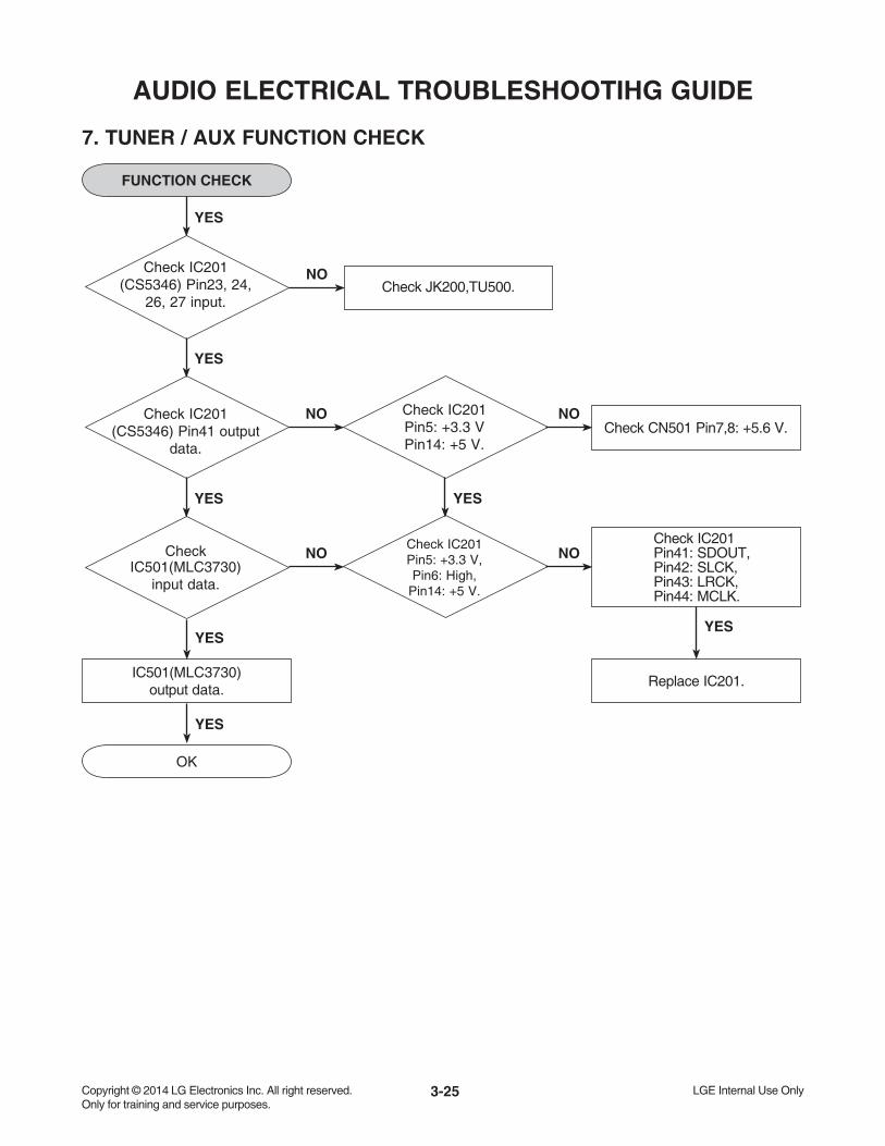
7. TUNER / AUX FUNCTION CHECK
FUNCTION CHECK
Check JK200,TU500.NO
YES
Check IC201(CS5346) Pin23, 24,
26, 27 input.
YES
YES
Check IC201(CS5346) Pin41 output
data.
YES
YES
Check IC201Pin5: +3.3 V Pin14: +5 V.
Check CN501 Pin7,8: +5.6 V.NONO
CheckIC501(MLC3730)
input data.
YES
Check IC201Pin5: +3.3 V, Pin6: High,
Pin14: +5 V.
Check IC201Pin41: SDOUT,Pin42: SLCK, Pin43: LRCK,Pin44: MCLK.
NONO
IC501(MLC3730)output data.
Replace IC201.
OK
YES
3-25
AUDIO ELECTRICAL TROUBLESHOOTIHG GUIDE
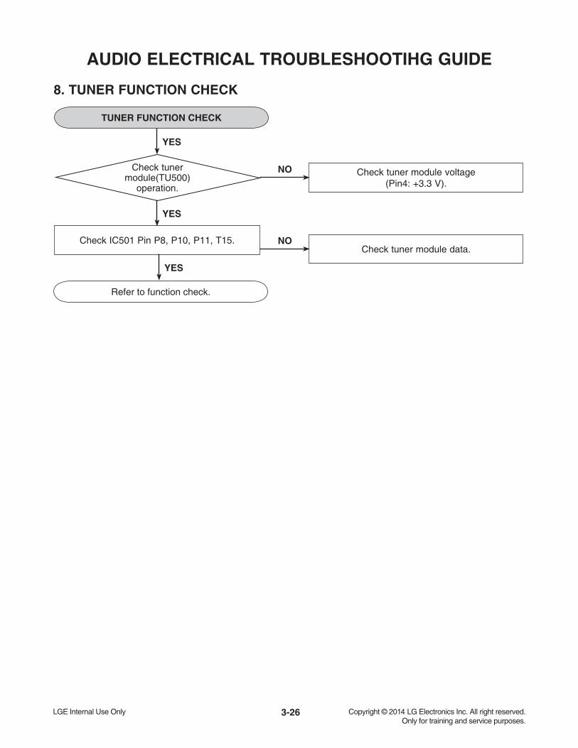
8. TUNER FUNCTION CHECK
TUNER FUNCTION CHECK
Check tuner module voltage(Pin4: +3.3 V).
NOCheck tunermodule(TU500)
operation.
YES
YES
Check IC501 Pin P8, P10, P11, T15.Check tuner module data.
NO
YES
Refer to function check.
3-26
AUDIO ELECTRICAL TROUBLESHOOTIHG GUIDE
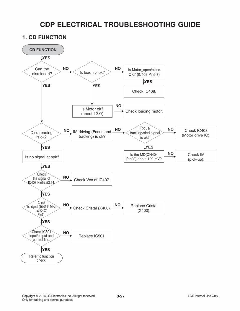
CD FUNCTION
YES
Can thedisc insert?
NO Is Motor_open/close OK? (IC408 Pin6,7)
NO
Refer to function check.
YES
Disc readingis ok?
Is no signal at spk?
YES
Is Motor ok?(about 12 Ω)
Is load +,- ok?
YES
Check the signal of
IC407 Pin52,53,54.NO
YES
Check the signal (16.0344 MHz)
at IC407 Pin51.
NO
YES
Check IC501input/output and
control line.
NO
YES
YES
Check loading motor.NO
IM driving (Focus and tracking) is ok?
NOFocus/
tracking/sled signalis ok?
NO Check IC408 (Motor drive IC).
NO
Is the MD(CN404Pin22) about 190 mV?
YES
Check Vcc of IC407.
Check Cristal (X400).NO Replace Cristal
(X400).
Replace IC501.
Check IC408.
YES
1. CD FUNCTION
Check IM(pick-up).
NO
3-27
CDP ELECTRICAL TROUBLESHOOTIHG GUIDE

USB FUNCTION
Check USB_5V. Display “NO USB”.
YES
YES
Check USB_D+/D-(R380,R381/ R382,R383).
YES
Plug-in usb device.
Check CN302.NONO
YES
Display “READ”.
YES
Display “NO FILE”.
YES
Check USB jack (JK301/ JK302).NO
Replace IC501.NO Check IC501
(Pin U7,U8/ A7,A8).
Check usb audio fi le in usb device (MP3, WMA fi le is playable)
YES
2. DOUBLE USB FUNCTION
3-28
CDP ELECTRICAL TROUBLESHOOTIHG GUIDE

1. SDRAM
1
2
3
4
CLK
DATA
ADDRESS
CS
2. SERVO
5
CD-16M
3-29
WAVEFORMS OF MAJOR CHECK POINT
IC502 PIN38
IC502 PIN53
IC502 PIN35
IC503 PIN1
IC501 PIN M1

3. AUDIO PATH
6
7
8
CD_BCK
CD_LRCK
CD_DATA
3-30
IC501 PIN N4
IC501 PIN N1
IC501 PIN N2
9
10
12
11
DAC_MCLK
DAC_BCK
DAC_LRCK
DAC_DATA
IC501 PIN D2
IC501 PIN E1
IC501 PIN D1
IC501 PIN E2
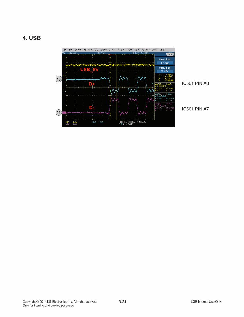
4. USB
13
USB_5V
D+
D-14
3-31
IC501 PIN A8
IC501 PIN A7

3-32
MEMO

3-33 3-34
23P10P
SPK TERMINAL TUN
ERM
OD
ULE
1 CD MD
MAIN + CD
19P
USB 2EA + FRONT
SMPS
15P
AUXJACK
1. [Total CNT : 6ea]
1. FFC Cable MAIN ↔ FRONT: 1EAMAIN ↔ MD: 2EAMAIN ↔ BT module: 1EA
SMPS ↔ MAIN : 1EAMAIN ↔ USB: 1EA
Power
cord
8P
: Harness
: FFC
BT
WIRING DIAGRAM

3-35 3-36
BLOCK DIAGRAMS 1. SYSTEM BLOCK DIAGRAM
DSP IC501
MLC3730
176PIN BGA
IC201CS5346
M
P/UP
IC408AM5890Motor Drive
SPDO/SLDO/FOD/TRD
OP_SW,CL_SW
A,B,C,D,E,F/ PD
MOT_MUTE/CLOSE/OPEN
SPIN
SLED
LOAD
IC407LC78615E
(New)LD/VREF
IM(CMS-S79RFVC6)
CD_16M
CD_MCK/RW/DIN_OUT/BUSYCD_RESB
CD_BCK/CD_LRCK/CD_DATA
ADC_RST/CLK/DAT
TUNER_L/RTUNER
AUX AUX_L/R
A
PTB_L/R
Portable
ADC_DATA
REMOCON/KEY
IC504EEPROM
SCL/SDA
VFDVFD_STB/CLK/DO
IC301ABOV
TUNERTUNER_L/R
TUNER_RST/CE/DAT/CLK
A
PWM DAT/CLKIC601
TAS5548PWM
FL
FR
FL
AMP_PDN
AMP_OTW/SD/CLIP/AMP PROTECT
FR
IC701AMP IC
TAS5612LA
SWIC702AMP IC
TAS5612LA
SW
PWM_RST
DAC_BCK/LRCK/DATA
PWM_MUTE
DAC_BCK/DAC_LRCK/DAC_MCLK
DRM_SEL/DRM_CKE/DRM_RASDRM_CLK/DRM_CAS/DRM_WEN
D0~D15/A0~A11/A13~A16
SF_DI/DO
SF_CS/CLK(SPI)
USB1_D
IC511IPOD 2.0C
CP_RESET/SCL/SDA
IC502 SDRAMM12L64164A
IC503 FLASHW25Q80BVSSIG
8MB
1MB/4MB
BT 4.0(New)RX/TX/RTS/CTS/RST/SDA/SCL
USB2_D
PTB_SENSE

2. SMPS BLOCK DIAGRAM
3-37 3-38
PVDD
NoiseFilterBlock(X-cap
Line Filter)
SnubberBlock
MainSMPS IC
Block
TRANS
SnubberBlock
Photo coupler
Photo coupler
Photo coupler
FL+FL-Vkk
On/Off
12V LDO 12V
5.6VA
P.CTL
On/Off
AMPSMPS ICWith FET
Block
FUSE
Y-Cap
Y-Cap
TRANS
CN901
Feedback
Feedback

3. AUDIO PATH BLOCK DIAGRAM
3-39 3-40
24MHZ
AMP Block
DSPBlock
PWM TAS5548
TAS5624AFR,FL
Woofer
Tuner
Aux in
ADCCS5346(SLAVE)
AUX
MLC3730(176 PIN)
DA
C_D
ATA
DAC_LRCK
DAC_BCKTUNER DAC_MCLK
12.288MHZ
DAC_LRCK
DAC_BCK TAS5624A
255Wx2
250Wx1
RFLC78615E
CD_BCK
CD_LRCK
CD_DATA
ADC_DATA
32.768KHZ
PORTABLEPORTABLE

4. POWER DIAGRAM
3-41 3-42
DVCC_5V
RS1G
P_C
TRL
RS1G 1SS355 3EA
VDD
CO
REVD
D33

3-43 3-44
CIRCUIT DIAGRAMS 1. SMPS CIRCUIT DIAGRAM
IMPORTANT SAFETY NOTICE
WHEN SERVICING THIS CHASSIS, UNDER NO CIRCUMSTANCES SHOULD THE ORIGINAL DESIGN BEMODIFIED OR ALTERED WITHOUT PERMISSIONFROM THE LG CORPORATION. ALL COMPONENTSSHOULD BE REPLACED ONLY WITH TYPES IDENTICAL TO THOSE IN THE ORIGINAL CIRCUIT. SPECIAL
COMPONENTS ARE SHADED ON THE SCHEMATICFOR EASY IDENTIFICATION.THIS CIRCUIT DIAGRAM MAY OCCASIONALLY DIFFER FROM THE ACTUAL CIRCUIT USED. THIS WAY,IMPLEMENTATION OF THE LATEST SAFETY ANDPERFORMANCE IMPROVEMENT CHANGES INTOTHE SET IS NOT DELAYED UNTIL THE NEW SERVICELITERATURE IS PRINTED.
NOTE :1. Shaded( ) parts are critical for safety.
Replace only with specified part number.2. Voltages are DC-measured with a digital voltmeter
during Play mode.
A
1
2
3
4
5
6
7
8
9
10
11
12
B C D E F G H I J K L M N O P Q R S T
CAUTION: Danger if fuse is incorrectly replaced.
Replace only with the type identical to fuse rating and(or) model name described in main label.
WarningParts that are shaded are critical withrespect to risk of fire or electrical shock.
SMPSEAX65422801_0.1.0_SMPS
2013. 12. 27

3-45 3-46
2. MAIN - DSP CIRCUIT DIAGRAM
4
6
7
8
5
10
11
12
9 14 13
1
2
3
: WAVEFORM NUMBER
A
1
2
3
4
5
6
7
8
9
10
11
12
B C D E F G H I J K L M N O P Q R S T
DSPEAX65586301_0.1.0_MAIN(#1)
2013. 12. 27

3-47 3-48
3. MAIN - SERVO CIRCUIT DIAGRAM
A
1
2
3
4
5
6
7
8
9
10
11
12
B C D E F G H I J K L M N O P Q R S T
SERVOEAX65586301_0.1.0_MAIN(#2)
2013. 12. 27

3-49 3-50
4. MAIN - ADC/ PWM CIRCUIT DIAGRAM
A
1
2
3
4
5
6
7
8
9
10
11
12
B C D E F G H I J K L M N O P Q R S T
ADC/PWMEAX65586301_0.1.0_MAIN(#3)
2013. 12. 27

3-51 3-52
5. MAIN - AMP CIRCUIT DIAGRAM
A
1
2
3
4
5
6
7
8
9
10
11
12
B C D E F G H I J K L M N O P Q R S T
AMPEAX65586301_0.1.0_MAIN(#4)
2013. 12. 27

3-53 3-54
6. FRONT CIRCUIT DIAGRAM
A
1
2
3
4
5
6
7
8
9
10
11
12
B C D E F G H I J K L M N O P Q R S T
FRONTEAX65586201_0.1.0_FRONT
2013. 12. 27

3-55 3-56
CIRCUIT VOLTAGE CHART 1. ICs
Location Pin No. SPEC EE Mode (V) Margin Playback Mode (V) Margin
IC503 Flash (W25Q64FVSSIG)
8(VDD) 2.7~3.6 3.24 - 3.24 -
IC504 EEPROM(M24C16)
8(VCC) 1.8~5.5 3.24 - 3.24 -
IC505 P-SENSE(AZ7027RTRE1)
1(VCC) <18 3.6 - 3.6 -
IC506 RESET(AZ7027RTRE1)
1(VCC) <18 3.15 - 3.16 -
IC507 LDO (TJ4220GDP-ADJ)
3(VIN) 2.5~6 4.91 - 4.88 -
6(VOUT) - 3.25 - 3.25 -
IC508 LDO (AZ1117BH-1.2TRE1)
2(OUTPUT) 1.176~1.224 1.19 - 1.19 -
3(INPUT) <15 3.24 - 3.24 -
IC509 LDO (AZ1117BH-1.2TRE1)
2(OUTPUT) 1.176~1.224 1.19 - 1.19 -
3(INPUT) <15 3.24 - 3.24 -
IC510 LDO (AZ1117BH-ADJ)
2(OUTPUT) <15 5.67 - 5.66 -
3(INPUT) <15 4.02 - 4.02 -
IC511 IPOD(MFI337S3959)
8(VCC) 1.6~5.5 3.24 3.24 -
IC601 PWM (TAS5548DGG)
9(AVDD) 2.97~3.63 3.25 - 3.24 -
14(DVDD2_CORE) 2.97~3.63 3.24 - 3.23 -
35(DVDD1_CORE) 2.97~3.63 3.24 - 3.23 -
50(AVDD_PWM) 2.97~3.63 3.24 - 3.23 -
IC701 AMP(TAS5624A)
1(GVDD_AB) 10.8~13.2 11.96 - 11.96 -
2(VDD) 10.8~13.2 12.12 - 12.12 -
22(GVDD_CD) 10.8~13.2 11.96 - 11.96 -
29,30,31(PVDD_CD) 12~34 37.5 - 37.5 -
36,37,38(PVDD_AB) 12~34 37.5 - 37.5 -
FRONT Board
IC301 VFD (MC3401L)
13(VDD) 3.0~5.5 3.24 -1.26 3.24 -1.26
43(VDD) 3.0~5.5 3.24 -1.26 3.24 -1.26
30(VEE) VDD-35 -22.4 -9.36 -22.5 -9.26
IC302 LDO (LM37102D)
2(VIN) 2.25~16 5.69 3.44 5.68 3.43
3(VOUT) - 5.05 - 5.05 -
Location Pin No. SPEC EE Mode (V) Margin Playback Mode (V) Margin
MAIN Board
IC201 ADC(CS5346)
5(VLC) 3.13~5.25 3.24 0.11 3.24 0.11
14(VA) 4.75~5.25 5.08 0.17 5.08 0.17
36(VLS) 3.13~5.25 3.24 0.11 3.24 0.11
46(VD) 3.13~3.47 3.24 0.11 3.24 0.11
IC202 LDO (LM37102D-ADJ)
2(VIN) 2.25~16 5.68 3.43 5.67 3.42
3(VOUT) - 5.08 - 5.08 -
IC407 SERVER (LC78615E)
18(AVDD) 3.0~3.6 3.24 0.24 3.24 0.24
28(VVDD1) 3.0~3.6 3.24 0.24 3.24 0.24
33(DVDD) 3.0~3.6 3.24 0.24 3.24 0.24
59(DVDD) 3.0~3.6 3.24 0.24 3.24 0.24
63(XVDD) 3.0~3.6 3.24 0.24 3.24 0.24
IC408 MOTOR(AM5890)
8(VCC1) 4.3~13.2 5.08 - 5.08 -
19(VCC2) 4.3~Vcc1 5.08 - 5.07 -
IC501 MPEG(MLC3730)
A4 (VDD33ADC) 3.0~3.6 3.24 - 3.24 -
B7 (VDDUSB11) 3.0~3.6 3.24 - 3.24 -
A9 (VDD12CORE) 1.08~1.32 1.18 - 1.18 -
A10 (VDD33IO) 3.0~3.6 3.24 - 3.24 -
E9 (VDD12CORE) 1.08~1.32 1.18 - 1.18 -
D14 (VDD33IO) 3.0~3.6 3.24 - 3.24 -
J14 (VDD12CORE) 1.08~1.32 1.18 - 1.18 -
P14 (VDD33IO) 3.0~3.6 3.24 - 3.24 -
T16(VDD30RTC) 2.75~3.3 3.15 - 3.16 -
T10 (VDD12ALIVE) 1.08~1.32 1.18 - 1.18 -
U9 (VDD33OSC) 3.0~3.6 3.24 - 3.24 -
P9 (VDD12USB20) 1.08~1.32 1.19 - 1.19 -
U6 (VDD33USB20) 3.0~3.6 3.24 - 3.24 -
U5 (VDD33USB20) 3.0~3.6 3.24 - 3.24 -
U4 (VDD12CORE) 1.08~1.32 1.18 - 1.18 -
P4 (VDD33IO) 3.0~3.6 3.24 - 3.24 -
J4 (VDD12INT) 1.08~1.32 1.18 - 1.18 -
D4 (VDD33IO) 3.0~3.6 3.24 - 3.24 -
IC502 SDRAM (W9812G6JH-6)
1(VDD) 3.0~3.6 3.24 - 3.24 -
3(VDDQ) 3.0~3.6 3.24 - 3.24 -
9(VDDQ) 3.0~3.6 3.24 - 3.24 -
14(VDD) 3.0~3.6 3.24 - 3.24 -
27(VDD) 3.0~3.6 3.24 - 3.24 -
43(VDDQ) 3.0~3.6 3.24 - 3.24 -
49(VDDQ) 3.0~3.6 3.24 - 3.24 -

3-57 3-58
2. CAPACITORS
Loca. No.Value
Capacitor (uF)
EEMode Play back
Voltage_Spec
Positive (+)
Negative (-)
Gap MarginPositive
(+)Negative
(-)Gap Margin
MAIN Board
C244 47uF 16V 5.08V 0V 5.08V 10.92V 5.08V 0V 5.08V 10.92V
C402 100uF 16V 5.08V 0V 5.08V 10.92V 5.08V 0V 5.08V 10.92V
C404 47uF 16V 3.24V 0V 3.24V 12.76V 3.23V 0V 3.23V 12.77V
C429 220uF 10V 5.08V 0V 5.08V 4.92V 5.07V 0V 5.07V 4.93V
C479 220uF 10V 1.68V 0V 1.68V 8.32V 1.68V 0V 1.68V 8.32V
C481 47uF 16V 3.24V 0V 3.24V 12.76V 3.23V 0V 3.23V 12.77V
C501 1000uF 6.3V 3.16V 0V 3.16V 3.14V 3.16V 0V 3.16V 3.14V
C526 47uF 16V 1.19V 0V 1.19V 14.81V 1.19V 0V 1.19V 14.81V
C541 47uF 16V 1.19V 0V 1.19V 14.81V 1.19V 0V 1.19V 14.81V
C579 10uF 16V 3.24V 0V 3.24V 12.76V 3.24V 0V 3.24V 12.76V
C618 100uF 16V 3.25V 0V 3.25V 12.75V 3.25V 0V 3.25V 12.75V
C624 100uF 16V 12.12V 0V 12.12V 3.88V 12.12V 0V 12.12V 3.88V
C643 100uF 16V 5.08V 0V 5.08V 10.92V 5.08V 0V 5.08V 10.92V
C724 470uF 50V 37.5V 0V 37.5V 12.5V 37.5V 0V 37.5V 12.5V
C727 470uF 50V 37.5V 0V 37.5V 12.5V 37.5V 0V 37.5V 12.5V
C737 470uF 50V 37.5V 0V 37.5V 12.5V 37.5V 0V 37.5V 12.5V
FRONT Board
C310 220uF 10V 3.24V 0V 3.24V 6.76V 3.24V 0V 3.24V 6.76V
C316 100uF 16V 3.16V 0V 3.16V 12.84V 3.14V 0V 3.14V 12.86V
C377 47uF 50V -18.1V 0V -18.1V 68.1V -18.2V 0V -18.2V 68.2V
Location No. SPEC Test (V)
SMPS Board
C904 180uF/450V 315
C909 22uF/50V 14.7
C911 47uF/50V 18
C914 10uF/50V 17.4
C931 220uF/16V 2.9
C932 47uF/50V 22.9
C933/C934 1000uF/16V 5.5
C935/C936 100uF/50V 13.5
C954/C955 2200uF/50V 37.4
MEMO

3-59 3-60
PRINTED CIRCUIT BOARD DIAGRAMS 1. SMPS P.C.BOARD (TOP VIEW)
(BOTTOM VIEW) NOTE) Warning
Parts that are critical with respect to risk of fire or electrical shock.
3-61 3-62
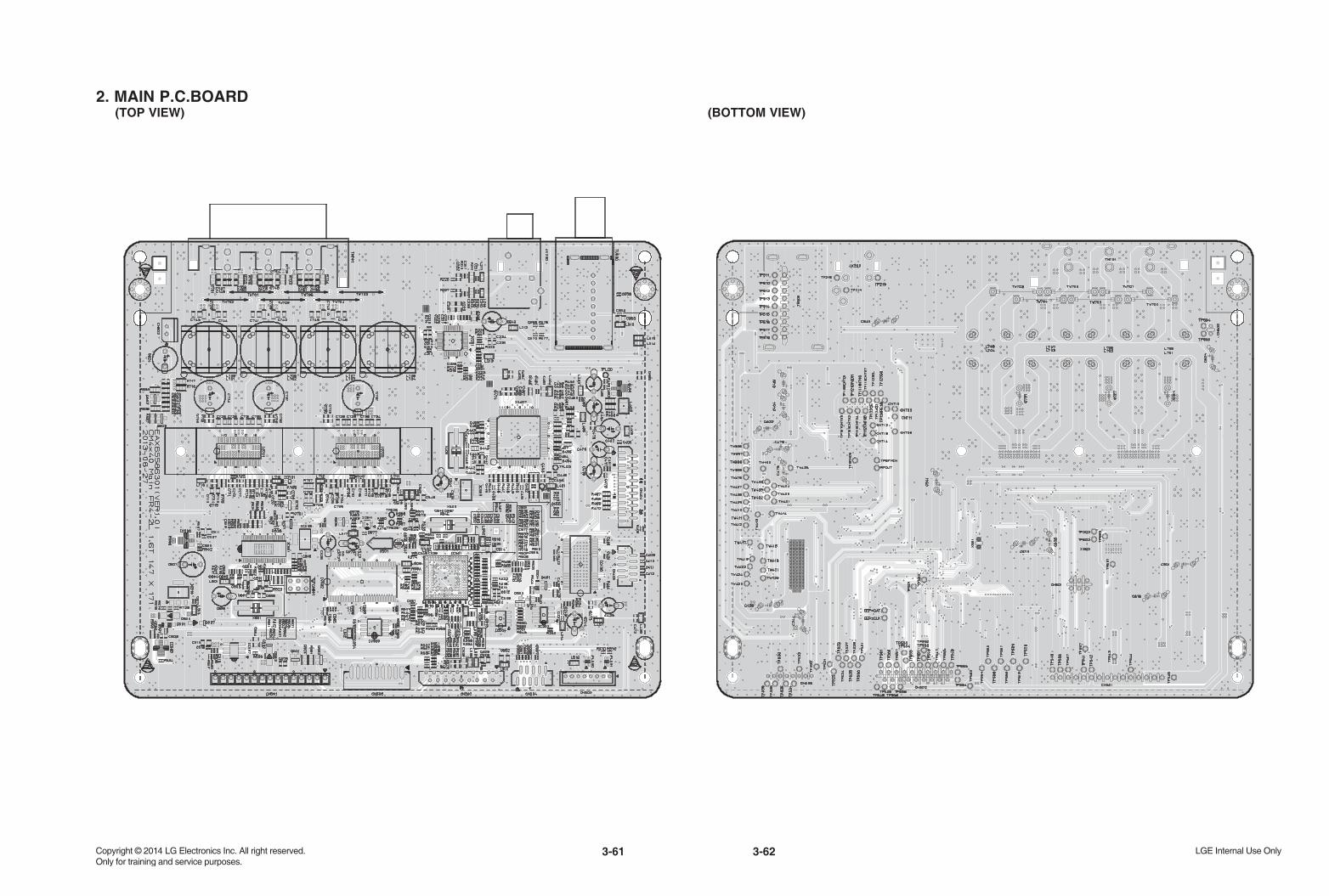
2. MAIN P.C.BOARD (TOP VIEW)
(BOTTOM VIEW)

3-63 3-64
3. FRONT P.C.BOARD (TOP VIEW) (BOTTOM VIEW)