AVR An Introductory Course
126
John Morton Newnes OXFORD AMSTERDAM BOSTON LONDON NEW YORK PARIS SAN DIEGO SAN FRANCISCO SINGAPORE SYDNEY TOKYO fl.Wl
-
Upload
khangminh22 -
Category
Documents
-
view
2 -
download
0
Transcript of AVR An Introductory Course
John Morton
NewnesOXFORD AMSTERDAM BOSTON LONDON NEW YORK PARIS SAN DIEGO
SAN FRANCISCO SINGAPORE SYDNEY TOKYO
fl.Wl
Newnes
An imprint of Elsevier Science
Linacre House, Jordan Hill, Oxford 0X2 8DP
225 Wildwood Avenue, Woburn, MA 01801-2041
First published 2002
Copyright © 2002, John Morton. All rights reserved
Contents I
The right of John Morton to be identified as the author of this work has been
asserted in accordance with the Copyright. Designs and Patent Act 1988
No part of this publication may be reproduced in any material form (including
photocopying or storing in any medium by electronic means and whether or not
transiently or incidentally to some other use of this publication) without the written
permission of the copyright holder except in accordance with the provisions of the
Copyright. Designs and Patents Act 1988 or under the terms of a licence issued by
the Copyright Licensing Agency Ltd. 90 Tottenham Court Road London. England
WIT 4LP. Applications for the copyright holder's written permission to reproduce
any part of this publication should be addressed to the publishers
British Library Cataloguing in Publication Data
Morton. John. 1980—
AVR: an introductory course
1. Programmable controllers 2. Integrated circuits - Design and construction
.^Microelectronics
I. Title ^626.8'9
ISBN 0 7506 56352
For information on all Newnes publications visit our website
at www.newnespress.com
Typeset by Avocet Typeset, Brill, Aylesbury. Bucks
Printed in Great Britain by Biddles Ltd Guildford and King’s Lynn
Acknowledgements
Prefaceix
xi
1 Introduction
Short bit for PIC users
Number systems
Adding in binary
Negative numbersAn 8-bit Flash microcontroller
Initial steps
Choosing vour model
Flowchart
Writing
Assembling
Registers
Instructions
Program template
2 Basic Operations with AT90S1200 and Tinyl2Program A: LED on
AVR Studio - AssemblingAVR Studio - Simulating
Emulating
Hardware
AVR Studio - ProgrammingFuse bits
Programs B and C: Push ButtonSeven Segment displays and indirect addressing
Programs D and E: Counter
Timing
Program F: Chaser
Timing without a timer?
The Program Counter and SubroutinesProgram G: Counter v.3.0
24
24
25
26
27
27
30
31
31
34
39
44
47
52
54
57
o->
UJ
lo
vi Contents
Program H: Traffic Lights
Logic Gates
Program I: Logic Gate Simulator
^SREG - The Status Register
Watchdog Timer
Sleep
More Instructions - loose ends
Major Program J: Frequency Counter
Introducing the rest of the family
Intermediate Operations
Interrupts
Program K: Reaction Tester
Analogue Comparator
Program L: 4-bit analogue to digital converter
10-bit analogue to digital conversion (ADC)
Program M: Voltage Inverter
EEPROM16-bit Timer/Counter 1
Input Capture
Output Compare
Major Program N: Melody Maker
Advanced Operations
PWM - Pulse Width Modulation
DARTProgram 0: Keyboard Converter
Serial Peripheral Interface (SPI)
Tiny 15s Eccentric Timer 1
Shrtcts
A Mega SummaryFinal Program P: Computer Controlled Robot
Conclusions
Appendix A:
Appendix B:
Appendix C:
Appendix D:
Appendix E:
Appendix F:
Appendix G:
Appendix H:
Specifications for some PICs
Pin layouts of various AVRsInstruction overview
Instruction glossary
Interrupt vector tables
Hex conversion
ASCII conversion
When all else fails, read this
Contents vii
Appendix I: Contacts and further reading 169
Appendix J: Sample programs 170
Program A. Led on - turns an LED on 1 70
Program B. Push button (1.0) - turns an LED on when a button is
pressed 171
Program C. Push button (2.0) - shorter version of push button
(1.0) 172
Program D. Counter (1.0) - counts push button presses on a
seven segment display 1 73
Program E. Counter (2.0) - as counter (1 .0) reduces multiple
reads , 1 74
Program F. Chaser - chases LED display at variable speeds 1 76
Program G. Counter (3.0) - as counter (2.0) with button
bounce solved 178
Program H. Traffic - pedestrian crossing traffic lights simulator 180
Program I. Logic gates - simulates eight different logic gates 1 83
Program J. Frequency counter - measures frequency between
1 Hz and’ 1 MHz ’
184
Program K. Reaction tester - measures human reaction time 191
Program L. 4-bit analogue to digital converter - how to make a
comparator into an ADC 1 97
Program M. Voltage inverter - converts V into (5 - V) 199
Program N. Melody maker - plays programmable tunes 200
Program O. Keyboard converter - turns your computer keyboard
into a musical one 204
Program P. Computer controlled robot 208
Answers to exercises 218
Index 237
/
Acknowledgements
Robert Czarnek first introduced me to AVRs, and ! quickly recognized their
strengths over other microcontrollers. The only relative weakness that I saw in
them was a lack of fame on the scale of the Microchip s PIC, for example. I
knew it was only a matter of time before this would be steadily overcome and
this book is a guide for those with little or no microcontroller background to
start using AVRs.
I would like to take this opportunity to thank those who have assisted me with
what you see before you. Atmel UK kindly donated a sample of their equip-
ment, though I assure you I remain impartial and objective! A big thanks must
go to Matt Webb for his efficient and meticulous proofreading, which often
consisted of writing4
What s this?* all over the page. He really had much better
things to do, for example passing his finals, but still managed to tear himself
away to comb through my pages. 1 would also like to thank Richard George for
his suggestions of example projects and general ideas. Thanks to Matt Harrison
for his help with the illustrations - he is off to further this calling at the Royal
College of Art. Finally, I must thank Max Horsey for his great generosity, as-
sistance and advice, and also the Electronics Department at Radley College,
Abingdon, for the continuing use of their excellent lab.
John Morton
J

reface
Congratulations! By reading this you're showing an interest in one of the most
capable and versatile 8-bit microcontrollers on the market, the AVR. Continue
reading this book to learn about the entire AVR family, and how they can help
simplify the design of your electronics projects as well as allow you to create
more sophisticated products.
Like all microcontrollers. AVRs allow tailor-made solutions which remain at
the same time completely flexible. However. AVRs are efficient, fast, and easy
to use microcontrollers, making them an ideal choice for designers. In this book
I begin from the most basic principles of microcontroller programming, such as
binary and hexadecimal, and cover the principal steps in developing a program.
Each AVR topic is introduced alongside one of twenty worked examples, which
include a pedestrian-crossing simulator, melody generator, frequency counters
and a computer-controlled robot.
To begin with, the programs are largely developed for you. However, as you
progress through each chapter, more and more of the programs will be written
by you in the form of the exercises, which appear throughout the book with
answers given at the end of the book. The appendices summarize the key prop-
erties of the most popular AVRs allowing quick reference without having to
plough through piles of datasheets.
In short this book offers a hands on approach to learning to program AVRs,and will provide a useful source of information for AVR programmers.
John Morton
1
Introduction
An AVR is a type of microcontroller, and not just any microcontroller - AVRsare some of the fastest around. I like to think of a microcontroller as a useless
lump of silicon with amazing potential. It will do nothing without but almost
anything with the program that you write. Under your guidance, a potentially
large conventional circuit can be squeezed into one program and thus into one
chip. Microcontrollers bridge the gap between hardware and software - they run
programs, just like your computer, yet they are small, discrete devices that can
interact with components in a circuit. Over the years they have become an indis-
pensable part of the toolbox of electrical engineers and enthusiasts as they are
perfect for experimenting, small batch productions, and projects where a certain
flexibility of operation is required.
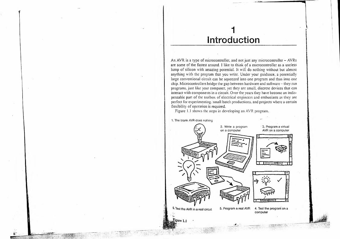
Figure 1.1 shows the steps in developing an AVR program.
1. The blank AVR does nothing
d2. Write a program
on a computer
3. Program a virtual
AVR on.a computer
Test the AVR in a real circuit
v- E*SUreU •
5. Program a real AVR 4. Test the program on a
computer
2 Introduction
The AYR family covers a huge range of different devices, from Tiny 8-pin
devices to the Mega 40-pin chips. One of the fantastic things about this is that
you can write a program with one type ofAVR in mind, and then change your
mind and put the program in a different chip with only minimal changes.
Furthermore, when you learn how to use one AVR, you are really learning how
to use them all. Each has its own peculiarities - their own special features but
underneath they have a common heart.
Fundamentally, AVR programming is all to do with pushing around numbers.
The trick to programming, therefore, lies in making the chip perform the desig-
nated task by the simple movement and processing of numbers. There is a
specific set of tasks you are allowed to perform on the numbers - these are
called instructions. The program uses simple, general instructions, and also
more complicated ones which do more specific jobs. The chip will step through
these instructions one by one, performing millions every second (this depends
on the frequency of the oscillator it is connected to) and in this way perform its
job. The numbers in the AVR can be:
1. Received from inputs (e.g. using an input ‘port’)
2. Stored in special compartments inside the chip
3. Processed (e.g. added, subtracted, ANDed multiplied etc.)
4. Sent out through outputs (e.g. using an output ‘port’)
This is essentially all there is to programming ('great* you may be thinking).
Fortunately there are certain other useful functions that the AVR provides us
with such as on-board timers, serial interfaces, analogue comparators, and a
host of ‘flags’ which indicate whether or not something particular has happened,
which make life a lot easier.
We will begin by looking at some basic concepts behind microcontrollers,
and quickly begin some example projects on the AT90S 1 200 (which we will call
1200 for short) and Tiny AVRs. Then intermediate operations will be intro-
duced, with the assistance of more advanced chips (such as the AT90S2313).
Finally, some of the more advanced features will be discussed, with a final
project based around the 2313. Most of the projects can be easily adapted for
any type ofAVR, so there is no need for you to go out and buy all the models.
Short bit for PIC users
A large number pf readers will be familiar with the popular PIC microcon-
troller. For this reason I’ll mention briefly how AVRs can offer an improvement
to PICs. For those ofyou who don’t know what PICs are, don’t worry too much
if you don’t understand all this, it will all make sense later on!
Basically, the AVRs are based on a more advanced underlying architecture,
and can execute an instruction every clock cycle (as opposed to PICs which
execute one every four clock cycles). So for the same oscillator frequency, the
AVRs will run four times as fast. Furthermore they also offer 32 working regis*^
Sg' * VL i A
Introduction 3
ter (compared w,th the one that PICs have), and about three times as manyinstructions, so programs will almost always be shorter. It is worth notin«however, that although the datasheets boast 90-120 instructions, there is conSerable repetition and redundancy, and so in my view there are more like 50distinct instructions.
Furthermore, what are known as special function registers on PICs (andblown as input/output registers on the AVR) can be directly accessed with PICs
tint1
ZtTlZTuirectlyVhe pons)> and this cannot be done t0 the
tent with AVRs. However, these are minor quibbles, and AVR programs willbe more efficient on the whole. All AVRs have flash program memory (so canbe rewritten repeatedly), and finally, as the different PICs have been developedover a period of many years there are some annoying compatibility issuesbetween some models which the AVRs have managed m avoid so far.
'
Number systems
tovS;„in
rvR"CinS 21 ,his s,as,"he difrer'm "™berins V*'™ which «Zr iprogramming: binary, decimal and hexadecimal. A binarymber is a base _ number (i.e. there are only two types of disit (0 and 1 )) asopposed to decimal - base 10 - with 1 0 different digits (0 to 9)rLikewise hexa-
ecimal represents base 16 so it has 16 different digits (0. 1, 2. 3, 4. 5. 6. 7 8. A, B, C, D. E and F). The table below shows how to count usinti the differentsystems- c “““
binary (8 digit)
00000000
00000001
00000010
00000011
00000100
00000101
00000110
00000111
00001000
00001001
00001010
00001011
00001100
00001101
00001110
00001111
00010000
00010001
etc.
decimal (3 disit)
000
001
002
003
004
005
006
007
008
009
010
011
012
013
014
015
016
017
hexadecimal (2 digit)
00
01
02
03
04
05
06
07
08
09
OA0BOC
4 Introduction
The binary digit (or bit) furthest to the right is known as the least significant
bit or Isb and also as bit 0 (the reason the numbering starts from 0 and not from
1 will soon become clear). Bit 0 shows the number of ‘ones’ in the number.
One equals 2°. The bit to its left (bit 1) represents the number of ‘twos’, the
next one (bit 2) shows the number of ‘fours’ and so on. Notice how two = 2 1
and four = 22 , so the bit number corresponds to the power of two which that
bit represents, but note that the numbering goes from right to left (this is very
often forgotten!). A sequence of 8 bits is known as a byte. The highest number
bit in a binary word (e.g. bit 7 in the case of a byte) is known as the most signif-
icant bit (msb).
So to work out a decimal number in binary you could look for the largest
power of 2 that is smaller than that number and work your way down.
Example 1.1 Work out the binary equivalent of the decimal number 83.
Largest power of two less than 83 = 64 = 26 . Bit 6 = 1
This leaves 83 - 64 = 19 32 is greater than 19 so bit 5 = 0,
16 is less than 19 so bit 4=1,This leaves 19-16 = 3 8 is greater than 3 so bit 3 = 0,
4 is greater than 3 so bit 2 = 0.
2 is less than 3 so bit 1 = 1,
This leaves 3-2=1 1 equals 1 so bit 0 = 1.
So 1010011 is the binary equivalent.
There is, however, an alternative (and more subtle) method which you may find
easier. Take the decimal number you want to convert and divide it by two. If
there is a remainder of one (i.e. it was an odd number), write down a one. Then
divide the result and do the same writing the remainder to the left of the
previous value, until you end up dividing one by two, leaving a one.
Example 1.2 Work out the binary equivalent of the decimal number 83.
Divide 83 by two. Leaves 41, remainder 1
Divide 41 by two. Leaves 20, remainder 1
Divide 20 by two. Leaves 10, remainder 0
Divide 10 by two. Leaves 5. remainder 0
Divide 5 by two. Leaves 2, remainder 1
Introduction 5
Likewise, bit 0 of a hexadecimal is the number of ones (16° = 1) and bit 1 is thenumber of 16s (16
1 = 16) etc. To convert decimal to hexadecimal (it is oftenabbreviated to just ‘hex’) look at how many 16s there are in the number, andhow many ones.
Example 1.3 Convert the decimal number 59 into hexadecimal. There are 316s in 59, leaving 59 - 48 = 1 1. So bit 1 is 3. 1 1 is B in hexadecimal, so bit 0is B. The number is therefore 3B.
exercise 1.3 Find the hexadecimal equivalent of 199.
exercise 1.4 Find the hexadecimal equivalent of 170.
One of the useful things about hexadecimal, which you may have picked upfrom Exercise 1.4, is that it translates easily with binary. If you break up abinary number into 4-bit groups (called nibbles
, i.e. small bytes), these little
groups can individually be translated into 1 hex digit.
Example 1.4 Convert 01101001 into hex. Split the number into nibbles: 0110and 1001. It is easy to see 0110 translates as 4 + 2 = 6 and 1001 is 8 + [=9.So the 8-bit number is 69 in hexadecimal. As you can see. this, is much morestraightforward than with decimal, which is why hexadecimal is morecommonly used.
exercise 1.5 Convert 11100111 into a hexadecimal number.
Adding in binaiy
Binary addition behaves in exactly the same way as decimal addition. Examineeach pair of bits.
0 + 0 = 0
1 + 0=11 + 1=0
1 +0+0=
1
1 + 1 +0 = 0
1 + 1 + 1 = 1
J
1 1 in decimal
no carry
no carry
carry 1
no carry
carry 1
carry 1
6 Introduction
EXERCISE 1.6 Find the result of 0101 1010 + 00001 1 1 1 using binary addition.
Negative numbers
We have seen how positive decimal numbers translate into binary, but how do
we translate negative numbers? We have to sacrifice a bit towards giving the
number a sign, so for a 4-bit signed number, the range of values might be 7 to
+8. There are various representations for negative numbers, including twos
complement. With this method, to make a positive number onto its negative
equivalent, you invert all the bits and then add one:
Example 1.6 0111 = 7
Invert all bits: 1 000
Add one: 1001
1001 = -1
Example U 1000 = 8
Invert: 0111
Add one: 1000
1000 = -8 = +8 FAIL
!
As vou can see in Example 1 .7. we cannot use -8 because it is indistinguishable
from +8. This asymmetry is recognized as an unfortunate consequence of the
two's complement method, but it has been accepted as the best given the short-
comings of other methods of signing binary numbers. Lets test these negative
numbers by looking at -2 + 7:
Example 1.8 2 = 001 0 therefore -2 = 1110
1110 = -2
+ 0111 =70101 =5 Which is what we would expect!
EXERCISE 1.7 Find the 8-bit two's complement representation of-40. and show
that -40 + 50 gives the expected result.
A result of this notation is that we can simply test the most significant bit (msb)
to see whether a number is positive or negative. A 1 in the msb indicates a nega-
tive number, and a 0 indicates positive. However, when dealing with the result
of addition and subtraction with large positive or negative numbers, this can be
misleading.
Introduction 7
Example 1.9 69 + 120 = ...
1
01000101 = + 69
+ 01 11 1000 = + 120
10111101 =+ 189 or -67
In other words, in the two’s complement notation, we could interpret the result
as having the msb 1 and therefore negative. There is therefore a test for ‘two’s
complement overflow’ which we can use to determine the real sign of the result.
The ‘twos complement overflow’ occurs when:
• both the msb’s of the numbers being added are 0 and the msb of the result
is 1
• both the msb’s of the numbers being added are 1 and the msb of the result
is 0
The real sign is therefore given by a combination of the ‘two’s complement
overflow' result, and the state of the msb of the result:
Two’s complement
overflow?
MSB of result Sign
No 0 Positive
No 1 Negative
Yes 0 Negative
Yes 1 Positive
As you can see from Example 1.10, there is a two’s complement overflow, and
the msb of the result is 1, and so the sign of the answer is positive (+189) as we
would expect. You will be relieved to hear that much of this is handled auto-
matically by the AVR.
The ones complement is simply the result of inverting all the bits in a
number.
An 8-bit RISC Flash microcontroller?
We call the AVR an 8-bit microcontroller. This means it deals with numbers 8
bits long. The binary number 11111111 is the largest 8-bit number and equals
255 in decimal and FF in hex (work it out!). With AVR programming, different
notations are used to specify different numbering systems (the decimal number
11111111 is very different from the binary numbei/'llllllll)! A binary
number is shown like this: 0b00103000 (i.e. 0b...). Decimal is the default
system, and the hexadecimal numbers are written with a Ox, or with a dollar
sign, like this: 0x3A or $3A. Therefore:
8 Introduction
\ ObOOlOlOl 1 is equivalent to 43 which is equivalent to 0x2B
l .
When dealing with the inputs and outputs of an AVR, binary is always used,
with each input or output pin corresponding to a particular bit. A 1 corresponds
'
to what is known as logic 1, meaning the pin of the AVR is at the supply voltage
(e.°. +5 V). A 0 shows that the pin is at logic 0, or 0 V. When used as inputs,
the° boundary between reading a logic 0 and a logic 1 is half of the supply
voltage (e.g. +2.5 V).. .
You will also hear the AVR called a RISC microcontroller. This means it is a
Reduced Instruction Set Computer, i.e. has relatively few instructions. This
makes life slightly harder for the programmer (you or me), but the chip itself is
more simple and efficient.
The AVR is sometimes called a Flash microcontroller. This refers to the tact
that the program vou write for it is stored in Flash memory - memory which
can be written to again and again. Therefore you can keep reprogramming the
( same AVR chip - for hobbyists this means one chip can go a long way.
Initial steps
The process of developing a program consists of five basic steps:
1. Select a particular AVR chip, and construct a program flowchart
2. Write proaram (using Notepad. AVR Studio, or some other suitable devel-
opment software)
3. Assemble program (changes what you've written into something an A\ K
$.• will understand)
4. Simulate or Emulate the program to see whether or not it works
5. Program the AVR. This feeds what you’ve written into the actual AVR
Let’s look at some of these in more detail.
Choosing your model
As there are so many different AVRs to choose from, it is important you think
carefully about which one is right for your application. The name of the AVR
can tell vou some information about what it has, e.g.:
AT90S1200- SRAM memory ‘size 0’ = no SRAMCPU model No. 0
EEPROM data memory ‘size 2’ = 64 bytes
1 Kb of flash program memory
ifUlf
Introduction 9
Memory sizes:
01 2 3 4 5 6 7 8 9 A B0 32 64 128 256 512 IK 2K 4K 8K 16K 32K
bytes bytes bytes bytes bytes
The meaning of these terms may not be familiar, but they will be covered
shortly. The Tiny and Mega family have slightly different systems. You can get
a decent overview of some of the AVRs and their properties by checking out
Appendix A.*
exercise 1 .8 Deduce the memory properties of the AT90S85 1 5.
One of the most important features of the AVR, which unfortunately is not
encoded in the model name, is the number of input and output pins. The 1200
has 15 input/output pins (i.e. they have 15 pins which can be used as inputs or
outputs), and the 8515 has up to 32!
Example 1.10 The brief is to design a device to count the number of times a
push button is pressed and display the value on a single seven segment display
- when the value reaches nine it resets.
1. The seven segment display requires seven outputs
2. The push button requires one input
This project would therefore need a total of eight input/output pins. In this case
a 1200 would be used as it is one of the simplest models and has enough pins.
A useful trick when dealing with a large number of inputs and outputs is
called strobing. It is especially handy when using more than one seven segment
display, or when having to test many buttons. An example demonstrates it best.
Example 1.11 The brief is to design a counter which will add a number
between 1 and 9 to the current two-digit value. There are therefore nine push
buttons and two seven segment displays.
It would first appear that quite a few inputs and outputs are necessary:
1. The two seven segment displays require seven outputs each, thus a total
of 14
2. The push buttons require one input each. Creating a tptal of nine
The overall total is therefore 23 input/output pins, which would require a large
AVR such as the 8515 (which has 32 I/O pins); however, it would be unneces-
sary to use such a large one as this value can be cut significantly.
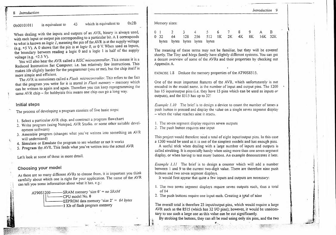
By strobing the buttons, they can all be read using only six pins, and the two
1 0 Introduction
seven segment displays can be controlled by only nine. This creates a total of 15
input/output (or I/O) pins, which would just fit on the 1200. Figure 1.2 shows
how it is done.
By making the pin labelled PBO logic 1 (+5 V) and PB1, PB2 logic 0 (0 V),
switches 1, 4 and 7 are enabled. They can then be tested individually by exam-
ining pins PB3 to PB5. Thus by making PBO to PB2 logic 1 one by one, all the
buttons can be examined individually. In order to work out how many I/O pins
you will need for an array ofX buttons, find the pair of factors ofX which have
the smallest sum (e.g. for 24, 6 and 4 are the factors with the smallest sum.
hence 6+4=10 I/O pins will be needed). It is better to make the smaller of the
two numbers (if indeed they are not the same) the number of outputs, and the
larger the number of inputs. This way the program takes less time to scroll
through all of the rows of buttons.
Strobing seven segment displays basically involves displaying a number on
one display for a short while, and then turning that display off while you display
another number on another display. PDO to PD6 contain the seven segment code
for both displays, and by making PB6 or PB7 logic 1. you can turn the indi-
vidual displays on. So the displays are in fact flashing on and off at high speed
giving the impression that they are constantly on. The programming require-
ments of such an arrangement will be examined at a later stage.
exercise 1.9 With the help of Appendix A, work out which model AVR you
would use for a four-digit calculator with buttons for digits 0-9 and five oper-
ations: +, x. *? and =.
Flowchart
After you have worked out how many I/O pins you will need and thus selected
a particular AVR, the next step is to create a program flowchart. This basically
forms the backbone of a program, and.it is much easier to write a program from
a flowchart than from scratch.
A flowchart should show the fundamental steps that the AVR must perform
and a clear program structure. Picture your program as a hedge maze. The flow-
chart is a rough map showing key regions of the maze. When planning your
flowchart you must note that the maze cannot lead off a cliff (i.e. the program
j
cannot simply end), or the AVR will run over the edge and crash. Instead the
m AVR is doomed to navigate the maze indefinitely (although you can send it to
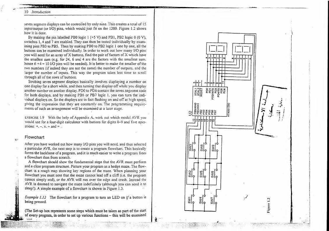
H sleep!). A simple example of a flowchart is shown in Figure 1.3.
H Example LI
2
The flowchart for a program to turn an LED on if a button is
11 being pressed.
'
(The Set-up box represents some steps which must be taken as part of the start
of every program, in order to set up various functions - this will be examined
later.) Rectangles with rounded corners should be used for start and finish
boxes, and diamond-shaped ones for decisions. Conditional jumps (the
diamond shaped boxes) indicate ‘//'something happens, thenjump somewhere'.
The amount of code any particular box will represent varies considerably, and
is really not important. The idea is to get the key stages, and come up with a
diagram that someone with no knowledge of programming would understand.
You will find it much easier to write a program from a flowchart, as you can
tackle each box separately, and not have to worry so much about the overall
structure.
exercise 1.10 Challenge! Draw the flowchart for an alarm with three push
buttons. Once the device is triggered by a pressure sensor, the three buttons
must be pressed in the correct order, and within 10 seconds, or else the alarm
will go off. If the buttons are pressed in time, the device returns to the state it
was in before being triggered. If the wrong code is pressed the alarm is trig-
gered. (The complexity of the answers will vary, but to give you an idea, my
answer has 13 boxes.)
Writing
Once you have finished the flowchart, the next step is to load up a program
template (such as the one suggested on page 19), and begin writing your
program into it. This can be done on a basic text package such as Notepad
(the one that comes with Microsoft Windows®), or a dedicated development
environment such as AYR Studio.
Introduction 13
Assembling
When you have finished writing your program, it needs to be assembled beforeit can be transferred onto a chip. This converts the program vou’ve written intoa series of numbers which can be fed into the Flash Program Memory of theAVR. This series of numbers is called the hex code or hexfile - a hex file willhave .hex after its name. The assembler will examine your program line by lineand try to convert each line into the corresponding hex code. If, however, it failsto recognize something in one of the lines of your code, it will register an errorfor that line. An error is something which the assembler thinks is definitelywrong - i.e. it can’t understand it. It may also register a warning - somethingwhich is probably wrong, i.e. definitely unusual but not necessarily wrong. Allthis should be made much more clear when we actually assemble our'firstprogram.
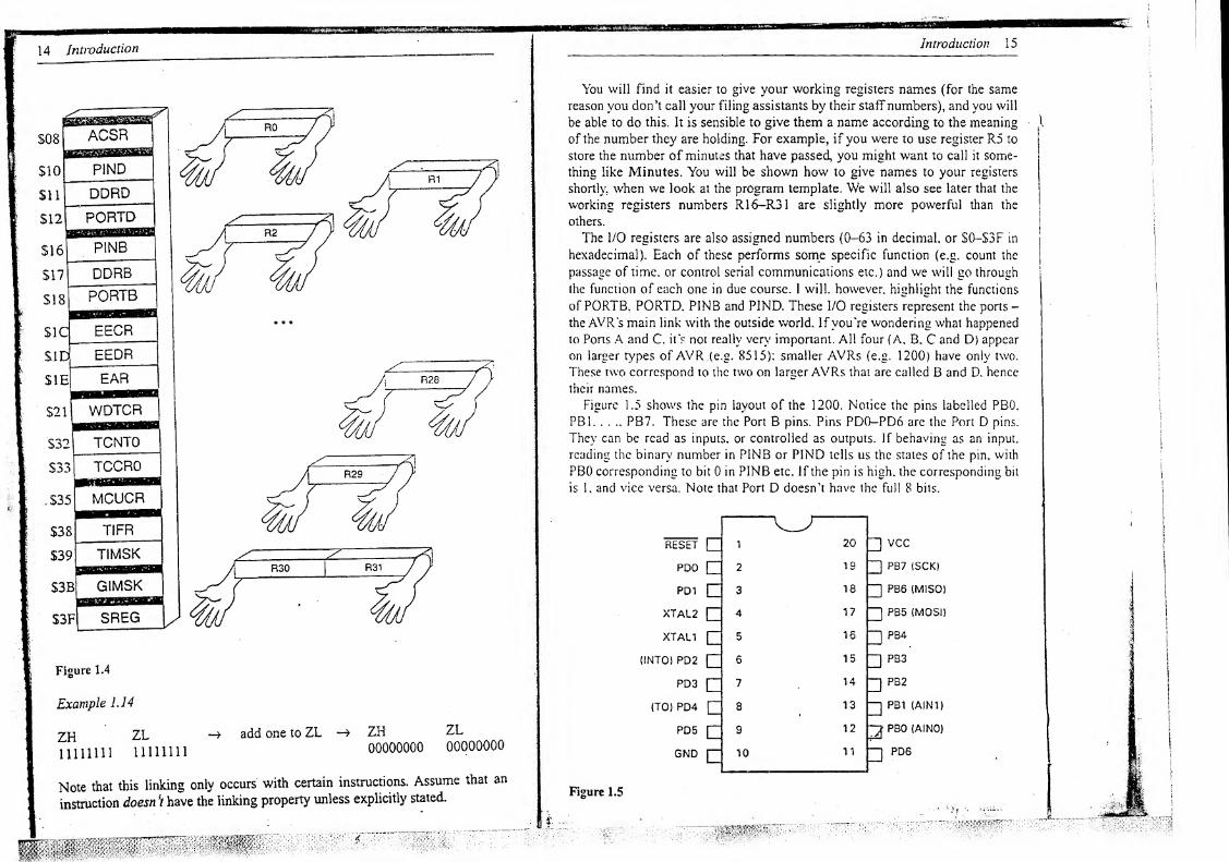
Registers
One of the most important aspects to programming with AVRs and microcon-trollers in general are the registers. I like to think of the AVR as having a largefiling cabinet with many drawers, each containing an 8-bit number (a byte).These drawers are registers - more specifically we call these the I/O registersIn addition to these I/O registers, we have 32 ‘working' registers - these aredifferent because they are not part of the filing cabinet Think of the workingregisters as the filing assistants, and yourself as the boss. If you want somethingput in the filing cabinet, you give it to the filing assistant, and then tell them toput it in the cabinet. In the same way, the program writer cannot move a numberdirectly into an I/O register. Instead you must move the number into a workingregister, and then copy the working register to the I/O register. You can also askyour filing assistants to do arithmetic etc. on the numbers they hold - i.e. youcan add numbers between working registers. Figure 1.4 shows the registers onthe 1200.
As you can see, each register is assigned a number. The working registers areassigned numbers R0, R1 R3 1. Notice, however, that R3(fand R31 areslightly different. They represent a double register called Z - an extra longregister that can hold a 16-bit number (called a word). These are two filingassistants that can be tied together. They can be referred to independently - ZLand ZH - but .can be fundamentally linked in that ZL (Z Lower) holds bits 0-7of the 16-bit number, and ZH (Z Higher) holds bits 8-15.
Example 1.13
ZH ZL00000000 11111111
add one to ZL ZH00000001
1 4 IntroductionIntroduction 15
Figure 1.4
Example 1.14
ZH ZL11111111 11111111
—> add one to ZL —> ZH00000000
ZL00000000
Note that this linking only occurs with certain instructions. Assume that an
instruction doesn ‘t have the linking property unless explicitly stated.
You will find it easier to give your working registers names (for the same
reason you don’t call your filing assistants by their staffnumbers), and you will
be able to do this. It is sensible to give them a name according to the meaning
of the number they are holding. For example, if you were to use register R5 to
store the number of minutes that have passed, you might want to call it some-
thing like Minutes. You will be shown how to give names to your registers
shortly, when we look at the program template. We will also see later that the
working registers numbers R16-R31 are slightly more powerful than the
others.
The I/O registers are also assigned numbers (0-63 in decimal, or S0-S3F in
hexadecimal). Each of these performs some specific function (e.g. count the
passage of time, or control serial communications etc.) and we will go through
the function of each one in due course. 1 will, however, highlight the functions
of PORTB, PORTD. P1NB and P1ND. These I/O registers represent the ports -
the AVR's main link with the outside world. If you're wondering what happened
to Pons A and C. its not really very important. All four (A. B, C and D) appear
on larger types of AVR (e.g. 8515): smaller AVRs (e.g. 1200) have only two.
These two correspond to the two on larger AVRs that are called B and D. hence
their names.
Figure 1.5 shows the pin layout of the 1200. Notice the pins labelled PBO,
PB1 PB7. These are the Port B pins. Pins PD0-PD6 are the Port D pins.
They can be read as inputs, or controlled as outputs. If behaving as an input,
reading the binary number in PINB or PIND tells us the states of the pin, with
PBO corresponding to bit 0 in PINB etc. If the pin is high, the corresponding bit
is 1, and vice versa. Note that Port D doesn’t have the full 8 bits.
RESET
PDO
PD1 CXTAL2
XTAL1
{INTO} PD2
PD3
(TO) PD4
PD5
GND
1
2
3
4
5
6
7
8
9
10
20
19
18
17
16
15
14
13
12
11
vcc
PB7 (SCK)
PB6 (MiSO)
PB5 (MOSi)
PB4
^ PB3
22PB2
2]PB1 (AIN1)
72 PBO (AIN0)
22pD6
Figure L5
1 6 Introduction
I Example 1.15 All ofPB0-PB7 are inputs. They are connected to push buttons
1 1 which are in turn connected to the +5 V supply rail. When all the buttons are
pressed, the number in PINB is Obi 1111111 or 255 in decimal. When all
I
|buttons except PB7 are pressed, the number in PINB is ObOl 111111 or 127 in
I I decimal.
m in a similar way, if the pin is an output its state is controlled by the corre-
% sponding bit in the PORTx register. The pins can sink or source 20 mA, and so
i are capable of driving LEDs directly.
f Example 1.16 All ofPB0-PB7 are outputs connected to LEDs. The other legs
I of the LEDs are connected to ground (via resistors). To turn on all of the LEDs.
|, the number Obi 1 1 1 1 1 1 1 is moved into PORTB. To turn off the middle two
\\ LEDs, the number Obi 1 1001 1 1 is moved into PORTB.:I
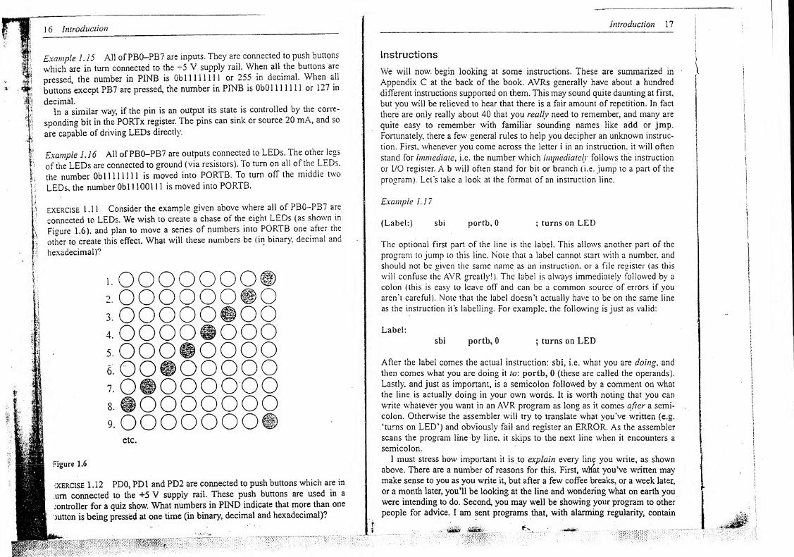
1 exercise 1.1 1 Consider the example given above where all of PB0-PB7 are
connected to LEDs. We wish to create a chase of the eight LEDs (as shown in
| Figure 1.6). and plan to move a series of numbers into PORTB one after the
t other to create this effect. What will these numbers be (in binary, decimal and
N hexadecimal)?
i.OOOOOOO®3.000001004.000000005 .000^0000tOOfOOOOO7 . 0^000000..iooooooo9 . 0000000®
Figure 1.6
•IXERCISE 1.12 PDO, PD1 and PD2 are connected to push buttons which are in
urn connected to the +5 V supply rail. These push buttons are used in a
controller for a quiz show. What numbers in PIND indicate that more than one
mutton is being pressed at one time (in binary, decimal and hexadecimal)?
Introduction 1
7
Instructions
We will now. begin looking at some instructions. These are summarized in
Appendix C at the back of the book. AVRs generally have about a hundred
different instructions supported on them. This may sound quite daunting at first,
but you will be relieved to hear that there is a fair amount of repetition. In fact
there are only really about 40 that you really need to remember, and many are
quite easy to remember with familiar sounding names like add or jmp.
Fortunately, there a few general rules to help you decipher an unknown instruc-
tion. First, whenever you come across the letter i in an instruction, it will often
stand for immediate, i.e. the number which immediately follows the instruction
or I/O register. A b will often stand for bit or branch (i.e. jump to a part of the
program). Let's take a look at the format of an instruction line.
Example 1.17
(Label:) portb, 0 ; turns on LED
The optional first part of the line is the label. This allows another part of the
program to jump to this line. Note that a label cannot start with a number, and
should not be given the same name as an instruction, or a file register (as this
will confuse the AYR greatly!). The label is always immediately followed by a
colon (this is easy to leave off and can be a common source of errors if you
aren't careful). Note that the label doesn’t actually have to be on the same line
as the instruction its labelling. For example, the following is just as valid:
sbi portb, 0;turns on LED
After the label comes the actual instruction: sbi. i.e. what you are doing , and
then comes what you are doing it to: portb, 0 (these are called the operands).
Lastly, and just as important, is a semicolon followed by a comment on what
the line is actually doing in your own words. It is worth noting that you can
write whatever you want in an AVR program as long as it comes after a semi-
colon. Otherwise the assembler will try to translate what you’ve written (e.g.
.‘turns on LED’) and obviously fail and register an ERROR. As the assembler
scans the program line by line, it skips to the next line when it encounters a
semicolon.
I must stress how important it is,to explain every line you write, as shown
above. There are a number of reasons for this. First, what you’ve written maymake sense to you as you write it, but after a few coffee breaks, or a week later,
or a month later, you’ll be looking at the line and wondering what on earth you
were intending to do. Second, you may well be showing your program to other
people for advice. I am sent programs that, with alarming regularity, contain
18 Introduction Introduction 1
9
very few or in some cases no comments at all. There is not much one can do in
this situation, as it is almost impossible to deduce the intended operation of the
program by looking at the bare code. Writing good comments is not necessarily
easy - they should be very clear, but not too long. It is particularly worth
avoiding falling into the habit ofjust copying out the meaning of the line..
Example 1.18
sbi PortB, 0 ;sets bit 0 of register PortB
A comment like the one above means very little at all, as it doesn’t tell you why
you’re setting bit 0 of register PortB, which after all is what the comment is
really about. If you want to get an overview of all the instructions offered, have
a good look at Appendix C and you can get a feel of how the different instruc-
tions are arranged. They will be introduced one by one through the example
projects which follow.
Program template
Most programs will have a certain overall structure, and there are certain
common elements needed for all programs to work. To make life easier, there-
fore, we can put together a program template, save it, and then load it every time
we want to start writing a program. A template that I like to use is shown in
Figure 1.7.
The box made up of asterisks at the top of the template is the program header
(the asterisks are there purely for decorative purposes). Filling these in makes it
,easier to find out what the program is without having to scroll down and read
the code and it helps you ensure that you are working on the most up-to-date
version of your program. Note that the contents of the box have no bearing on
the actual functioning of your program, as all the lines are preceded by semi-
colons. The ‘clock frequency:’ line refers to the frequency of the oscillator (e.g.
crystal) that you have connected to the chip. The AVR needs a steady signal to
tell it when to move on to the next instruction, and so executes an instruction
for every oscillation (or clock cycle). Therefore, if you have connected a 4 MHzcrystal to the chip, it should execute about 4 million instructions per second.
Note that I say about 4 million, because some instructions (typically the ones
which involve jumping around in the program) take two clock cycles, ‘for
AVR:’ refers to which particular AVR the program is written for. You will also
need to specify this further down.
Now we get to the lines which actually do something, .device is a directive
(an instruction to the assembler) which tells the assembler which device you are
using. For example, ifyou were writing this for the 1200 chip, the complete line
would be:
; Declarations:
.def temp =rl6
; Start of Program
rjmp Init : First line executed
Init: Idi temp, Obxxxxxxxx; Sets up inputs and outputs on PortB
out DDRB, templdi temp, Obxxxxxxxx
; Sets up inputs and outputs on PortDout DDRD, temp
>
ldi temp, Obxxxxxxxx; Sets pulls ups for inputs of PortB
out PortB, temp; and the initial states for the outputs
ldi temp, Obxxxxxxxx; Sets pulls ups for inputs of PortD
out PortD, temp; and the initial states for the outputs
, — —
; Main body of program:Start:
<write your program here>
rjmp Start; loops back to Start/
Figure 1.7
20 Introduction
.device at90sl200
Another important directive is .include, which enables the assembler to load
what is known as a look-up file . This is like a translator dictionary for the
assembler. The assembler will understand most of the terms you write, but it
may need to look up the translations of others. For example, all the names of the
input/output registers and their addresses are stored in the look-up file, so
instead of referring to $3F, you can refer to SREG. When you install the assem-
bler on your computer, it should come with these files and put them in a direc-
tory. I have included the path that appears on my own computer but yours may
well be different. Again, if the 1200 was being used, the complete line would1 be:
.include “C:\Program FiIes\Atmel\AVR StudioXAppnotesNnOOdef.inc”
Finally I’ll say a little about .nolist and .list. As the assembler reads your code,
it can produce what is known as a list file* which includes a copy of your
program complete with the assemblers comments on it. By and large, you do
not want this list file also to include the lengthy look-up file. You therefore write
.noiist before the .include directive, which tells the assembler to stop copying
things to the list file, and then you write .list after the .include line to tell the
assembler to resume copying things to the list file. In summary, therefore, the
.nolist and .list lines don’t actually change the working of the program, but they
will make your list file tidier. We will see more about list files when we begin
our first program.
*After the general headings, there is a space to specify somz declarations.
These are your own additions to the assembler’s translator dictionary - your
opportunities to give more useful names to the registers you will be using. For
example, 1 always use a working register called temp for menial tasks, and I've
assigned this name to R16. You can define the names of the working registers
using the .def directive, as shown in the template. Another type of declaration
that can be used to generally give a numerical value to a word is .equ. This can
be used to give your own names to I/O registers. For example. I might have
connected a seven segment display to all of Port B. and decided that I wish to
be able to write DisplayPort when referring to PortB. PortB is I/O register
number 0x18, so I might write DisplayPort in the program and the assembler
will interpret it as PortB:
.equ DisplayPort = PortB or
.equ DisplayPort = 0x18
Another example of where this might be useful is where a particular number is
used at different points in the program, and you might be experimenting and
changing tins number. You could use the .equ directive to give a*name to this
Introduction 21
number, and simply refer to the name in the rest of the program. When you thengo to change the number, you need only change the value in the .equ line andnot in all the instances of the use of the number all over the program. For themoment, however, we will not be using the .equ directive.
After the declarations, we have the first line executed by the chip on power-up or reset. In this line I suggest jumping to a section called Init which sets upall the initial settings of the AVR. This uses the rjmp instruction:
rjmp Init;
This stands for relative jump. In other words ifmakes the chip jump to a sectionof the program which you have labelled Init. The reason xvhv it is a relative-lump is in the way the assembler interprets the instruction, and so is not reallyimportant to understand. Say. for example, that the Init section itself was 40instructions further on from the rjmp Init line, the assembler would inter-pret the line as saying •jump forward 40 instructions' - i.e. a jump relative totheongma! instruction. Basically it is far easier to think of it as simply jumping
The first part of the Init section sets which pins are going to act as inputs,and which as outputs. This is done using the Data Direction I/O registers:DDRB and DDRD. Each bit in. these registers corresponds to a pin on the chip.For example, bit 4 of DDRB corresponds to pin PB4. and bit 2 ofDDRD corre-sponds to pin PD2. Now. setting the relative DDRx bit high makes the pin anoutput, and making the bit low makes the pin an input..-.,
..
If we configure a pin as an input; we then have the option of selectingwhether the input has a built-in pull-up resistor or not. This may save us thetrouble of having to include an external resistor. In order to enable the pull-upsmake the relevant bit in PORTx high; however, if you do not want them makesure you disable them by making the relevant bit in PORTx low. For the outputs,we want to begin with the outputs in some sort of start state (e.u. all off) andso for the output pins, make the relevant bits in PORTx hish or low dependingon how you wish them to start. An example should clear things up.
Example 1.19 Using a 1200 chip, pins PB0, PB4 and PB7 are connected topush buttons. We would like pull-ups on PB4 and PB7 onlv. Pins PD0 to PD6are connected to a seven segment display, and all other pins are not connected.All outputs should initially be off. What numbers should be written to DDRB.DDRD, PortB. and PortD to correctly specify the actions of the AVR’s pins?
First, look at inputs and outputs. PB0, 4 and 7 are inputs, the rest are notconnected (hence set as outputs). The number for DDRB is thereforeObOllOl l 10 . For Port D, all pins are outputs or not connected, hence thenumber for DDRD is Obll 11 111 .
To enable pull-ups for PB4 and PB7, make PortB, 4 and PortB, 7 high, all
22 Introduction
other outputs are initially low, so the number for PortB is OblOOlOOOO. All the
outputs are low for Port D, so the number for PortD is ObOOOOOOOG.
We can’t move these numbers directly into the I/O registers, but instead we
have first to move them into a working register (such as temp), and then output
the working register to the I/O register. There are a number of ways we can do
this:
Idi register, number ;
This loads the immediate number into a register, but it is very important to note
that this instruction cannot be used on all working registers - only on those
between- R1 6 and R3J (we can therefore still use it on temp, as that is R16). Wecan also use a couple of alternatives to this instruction if the number we wish to
move into the register happens to be 0 or 255/OxFF/Obl 1111111:
clr register ;
This clears the contents of a register (moves 0 into it) - note an advantage of
this over ldi is that it can operate on all working registers. Finally.
ser register :
This sets the contents of a register (moves 255/OxFF/Qbl 111111 into it), though
like ldi, it only works on registers between RJ6 and R3J.
We then need to move temp into the I/O register, using the following instruc*
tion:
out ioreg, reg
This moves a number out from a register, into an I/O register. Make sure you
note the order of the operands in the instruction - I/O register first, working
register second, it is easy to get them the wrong way round! We can therefore
see that the eight lines of the Init section move numbers into DDRB, DDRD.PortB and PortD via temp.
EXERCISE 1.13 Using a 1200 chip, pin PBO is connected to a pressure sensor,
and pins PB1. PB2 and PB3 control red, yellow and green LEDs respectively.
PDO to PD3 carry signals to an infrared transmitter, and PD4-PD6 carry signals
from an infrared receiver. All other pins are not connected. All outputs should
initially be off, and PBO should have a pull-up enabled. Write the eight lines that
will make up the Init section for this program.
After finishing the Init section, the program moves on to the main body of the
program labelled Start. This is where the bulk ofthe program will lie. Note that
jjillgi
351H
Introduction 23
* i fends the hne rJmP Start. Jt needn’t necessarily loop back I
hifhl’rU d°e
!ha?
‘° keep l00pin§ t0 someth‘ng, so you may want to alter • i 1hts last lme accordingly. At the end of the program, you can write .exit to tell
'
'
Thp flCCPmnlor rr\ LI.* Ai /»• , ..... 4,
&* ** I
the assembler to stop assembling the file, but this isn’t necessary as it will stopassembling anyway once it reaches the end of the file.
2Basic operations with
AT90S1 200 and TINY12
The best way to learn is through example and by doing things yourself. For the
rest of the book we will cover example projects, many of which will be largely
written by you. For this to work most effectively, it helps ifyou actually try these
programs, writing them out as you go along in Notepad or whatever develop-
ment environment you’re using. If you don’t have any special AVR software at
the moment, you can still write the programs out in Notepad and test them later.
First of all. copy out the program template covered in the previous chapter,
adjusting it as you see fit. and save it as template.asm. If you are using
Notepad make sure you select File Type as Any File. The .asm file extension
refers to assembly source. i.e. that which will be assembled.
Program A: LEDon
• Controlling outputs
Our first few programs will use the 1200 chip. Load up the template. Save Asto keep the original template unchanged and call the file ledon.asm. Make the
/appropriate adjustments to the headers etc. relevant to the 1200 chip (header,
.device, and .include). This first program is simply going to turn on an LED(and keep it on). The first step is to assign inputs and outputs. For this project
we will need only one output, and will connect it to RBO. The second step in the
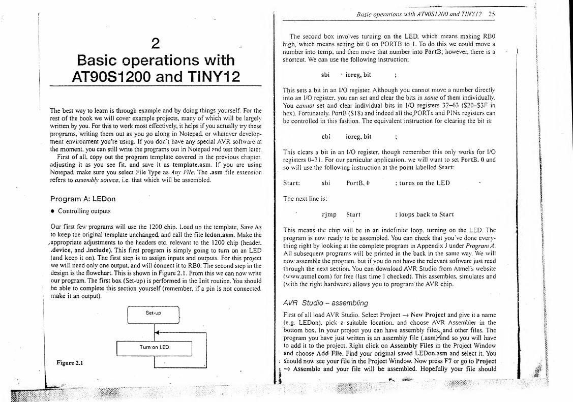
design is the flowchart. This is shown in Figure 2. 1 . From this we can now write
our program. The first box (Set-up) is performed in the Init routine. You should
! be able to complete this section yourself (remember, if a pin is not connected
make it an output).
Basic operations with AT90SJ200 and TINY12 25
The second box involves turning on the LED. which means making RBOhigh, which means setting bit 0 on PORTB to 1. To do this we could move a
number into temp, and then move that number into PortB; however, there is a
shortcut. We can use the following instruction:
sbi • ioreg, bit ;
This sets a bit in an I/O register. Although you cannot move a number directly
into an I/O register, you can set and clear the bits in some of them individually.
You cannot set and clear individual bits in I/O registers 32-63 (S20-S3F in
hex). Fortunately. PortB (SI 8) and indeed all theJPORTx and PINx registers can
be controlled in this fashion. The equivalent instruction for clearing the bit is:
cbi ioreg, bit ;
This clears a bit in an I/O register, though remember this only works for I/O
registers 0-31. For cur particular application, we will want to set PortB, 0 and
so will use the following instruction at the point labelled Start:
Start: sbi PortB, 0 ; turns on the LED
The next line is:
rjmp Start : loops back to Start
This means the chip will be in an indefinite loop, turning on the LED. The
program is now ready to be assembled. You can check that you’ve done every-
thing right by looking at the complete program in Appendix J under Program A.
All subsequent programs will be printed in the back in the same way. We will
now assemble the program, but if you do not have the relevant software just read
through the next section. You can download AVR Studio from Atmels website
(www.atmel.com) for free (last time 1 checked). This assembles, simulates and
(with the right hardware) allows you to program the AVR chip.
AVR Studio - assembling
First of all load AVR Studio. Select Project New Project and give it a name(e.g. LEDon), pick a suitable location, and choose AVR Assembler in the
bottom box. In your project you can have assembly files,, and other files. The
program you have just written is an assembly file (.asm)4nd so you will have
to add it to the project. Right click on Assembly Files in the Project Windowand choose Add File. Find your original saved LEDon.asm and select it. You
should now see your file in the Project Window. Now press F7 or go to Project
Assemble and your file will be assembled. Hopefully your file should
26 Basic operations with AT90S1200 and TINY12
assemble with no errors. If errors are produced you will find it helpful to
examine the List File (*.lst). Load this up in Notepad or some other text editor
and scan the document for errors. In this simple program, it is probably nothing
more than a spelling mistake. Correct any problems and then move on to
|
testing.
|
Testing
There are three main ways to test your program:
1. Simulating
2. Emulating
3. Programming an actual AVR and putting it in a circuit
The first of these, simulating, is entirely software based. A piece of software
pretends it’s an AVR and shows you how it thinks the program would run.
showing you how the registers are changing etc. You can also pretend to give it
inputs by manually changing the numbers in PINB etc. You can get a good idea
of whether or not the key concepts behind your program will work with this
kind of testing, but other real-word factors such as button-bounce cannot be
tested. Atmel's AVR Simulator comes with AVR Studio.
AVR Studio simulating
We will now have a go at simulating the LEDon program. After you assemble
your .asm file, double click on it in the Project Window to open it. Some of the
buttons at the top of the screen should now become active. There are three key
buttons involved in stepping through your program. The most useful one of
these, , is called Trace Into or Step Into. This runs the current line of your
program. Pressing this once will begin -the simulation and should highlight the
!first line of your program (rjmp lnit). You can use this button (or its
' shortcut FI I) to step through your program. We will see the importance of the
|
other stepping buttons when we look at subroutines later on in the book. In
|
order for this simulation to tell us anything useful, we need to look at how the
PO registers are changing (in particular bit 0 of PortB). This can be done by
going to View New 10 View. You can see that the 1/0 registers have been
grouped into categories. Expand the PortB category and this shows you the
PortB, DDRB and PinB registers. You can also view the working registers by-
going to View Registers. We will be watching R16 in particular, as this is
temp. Another useful shortcut is the reset button, (Shift + F5).
nn^nt^nUe stePP*n» through your program. Notice how temp gets cleared to
/nMvu^and als° cleared to 00, then temp is loaded with OxFF
p S’WWch is ften loaded in DDRB and DDRD. Then (crucially)
° act* 85 shown by die tick in the appropriate box. You may notice
Basic operations with AT90S1200 and TINY12 27
how this will automatically set PinB, bit 0 as well. Remember the difference
between PortB and PinB - PortB is a register representing what you wish to
output through the port, and PinB represents the actual, physical state of those
pins. For example, you could try to make an input high when the pin is acci-
dentally shorted to ground - PortB would have that bit high whilst PinB would
show the bit low', as the pin was being pulled low'.
Emulating
Emulating can be far more helpful in pinning dowrn bugs, and gives you a muchmore visual indication of the working of the program. This allows you to
connect a probe w'ith an end that looks like an AVR chip to your computer. The
emulator software then makes the probe behave exactly like an AVR chip
running your program. Putting this probe into your circuit should give you the
same result as putting a real AVR in, the great difference being that you can step
through the program slowly, and see the inner workings (registers etc.)
changing. In this way you are testing the program and the circuit board, and the
way they w'ork together. Unfortunately, emulators can be expensive - a sample
emulator is Atmel's ICE (ln-Circuit Emulator).
If you don't have an emulator, or after you've finished emulating, you* will
have lo program a real AVR chip and put it in your circuit or testing board. Oneof the great benefits ofAVRs is the Flash memory which allows you to keep
reprogramming the same chip, so you can quite happily program your AVR, see
if it works, make some program adjustments, and then program it again with the
new; improved code.
For these latter two testing methods you obviously need some son of circuit
or development board. If you are making your owm circuit, you will need to
ensure certain pins on the chip are wired up correctly. We will now' examine
howr this is done.
Hardware
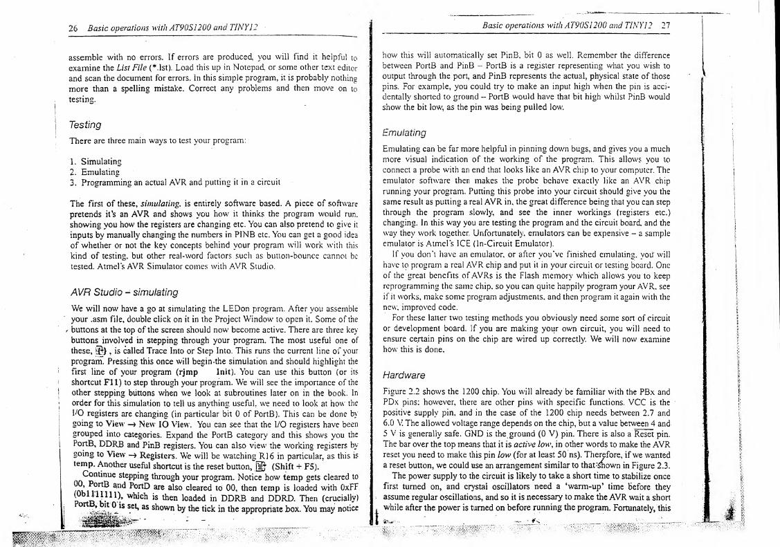
Figure 2.2 show's the 1200 chip. You will already be familiar with the PBx and
PDx pins: however, there are other pins w'ith specific functions. VCC is the
positive supply pin, and in the case of the 1200 chip needs between 2.7 and
6.0 V The allowed voltage range depends on the chip, but a value between 4 and
5 V is generally safe. GND is the. ground (0 V) pin. There is also a Reset pin.
The bar over the top means that it is active low, in other words to make the AVRreset you need to make this pin low (for at least 50 ns). Therefore, ifwe wanted
a reset button, we could use an arrangement similar to that :£nown in Figure 2.3.
The power supply to the circuit is likely to take a short time to stabilize once
first turned on, and crystal oscillators need a ‘warm-up’ time before they
> assume regular oscillations, and so it is necessary to make theAVR wait a short
*while after the power is turned on before running the program. Fortunately, this
t. t
—
—
28 Basic operations with AT90S1200 and TINY12
5V
Figure 2.3
little delay is built into the AVR (lasting about 1 1 ms); however, if you have a
particularly bad power supply or oscillator, and want to extend the length of this
‘groggy morning feeling* delay you can do so with a circuit such as that shown
in Figure 2.4. Increase the value of Cl to increase the delay.*
Basic operations with AT90S1200 and TINY12 29
+5V
Figure 2.4
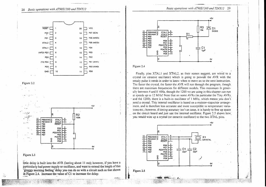
Finally, pins XTAL1 and XTAL2, as their names suggest, are wired to a
crystal (or ceramic oscillator) which is going to provide the AVR with the
steady pulse it needs in order to know when to move on to the next instruction.
The faster the crystal, the faster the AVR will run through the program, though,
there arc maximum frequencies for different models. This maximum is gener-
ally between 4 and 8 MHz. though the 1200 we are using in this chapter can run
at speeds up to 12 MHz! Note that on some AVRs (in particular the Tiny AVRsand the 1200). there is a built-in oscillator of 1 MHz. which means you don’t
need a crystal. This internal oscillator is based on a resistor-capacitor arrange-
ment. and is therefore less accurate and more susceptible to temperature varia-
tions etc.; however, if timing accuracy isn’t an issue, it is handy to free up space
on the circuit board and just use the internal oscillator. Figure 2.5 shows how;
you would wire up a crystal (or ceramic oscillator) to the two XTAL pins.
5V
30 Basic operations with AT9US1200 and TINY12
If you would like to synchronize your AVR with another device, or already
have a clock line with high-speed oscillations on it, you may want to simply
feed the AVR with an external oscillator signal. To do this, connect the oscil-
lator signal to XTAL1, and leave XTAL2 unconnected. Figure 2.6 shows how
using an HC (high-speed CMOS) buffer you can synchronize two AVR chips.
Figure 2.6
AVR Studio - programming
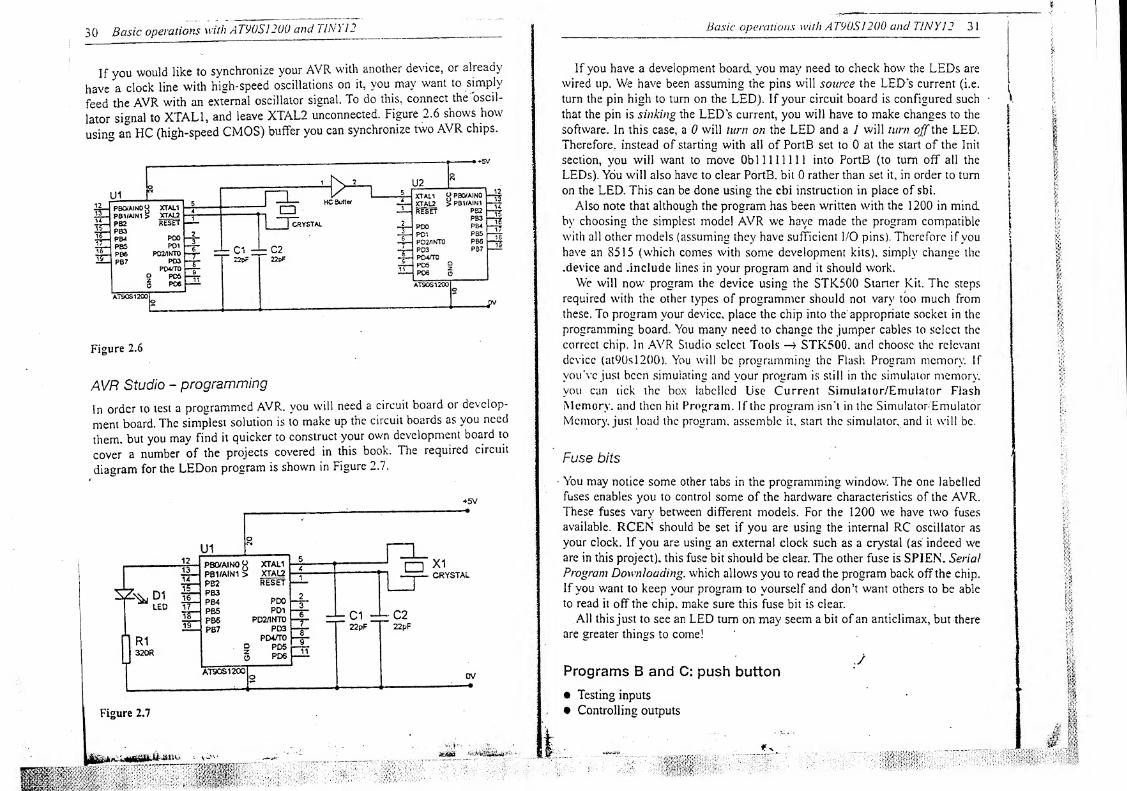
In order to test a programmed AVR, you will need a circuit board or develop*
ment board. The simplest solution is to make up the circuit boards as you need
them, but you may find it quicker to construct your own development board to
cover a number of the projects covered in this book. The required circuit
diagram for the LEDon program is shown in Figure 2.7.
5V
f
Basic operations with A T90S1200 and TINY}
2
31
If you have a development board, you may need to check how the LEDs are
wired up. We have been assuming the pins will source the LED’s current (i.e.
turn the pin high to turn on the LED). If your circuit board is configured such
that the pin is sinking the LED’s current, you will have to make changes to the
software. In this case, a 0 will turn on the LED and a 7 will turn off the LED.
Therefore, instead of starting with all of PortB set to 0 at the start of the Init
section, you will want to move Obi 11 11 111 into PortB (to turn off all the
LEDs). You will also have to clear PortB. bit 0 rather than set it, in order to turn
on the LED. This can be done using the cbi instruction in place of sbi.
Also note that although the program has been written with the 1200 in mind,
by choosing the simplest model AVR we have made the program compatible
with all other models (assuming they have sufficient I/O pins). Therefore if you
have an 8515 (which comes with some development kits), simply change the
.device and .include lines in your program and it should work.
We will now program the device using the STK500 Starter Kit. The steps
required with the other types of programmer should not vary too much from
these. To program your device, place the chip into the appropriate socket in the
programming board. You many need to change the jumper cables to select the
correct chip. In AVR Studio select Tools —> STK500. and choose the relevant
device (at90sl200). You will be programming the Flash Program memory. If
you've just been simulating and your program is still in the simulator memory,
you can tick the box labelled Use Current Simulator/Emulator Flash
Memory, and then hit Program. If the program isn't in the Simulator- Emulator
Memory, just load the program, assemble it. start the simulator, and it will be.
Fuse bits
You may notice some other tabs in the programming window. The one labelled
fuses enables you to control some of the hardware characteristics of the AVR.These fuses vary between different models. For the 1200 we have two fuses
available. RCEN should be set if you are using the internal RC oscillator as
your clock. If you are using an external clock such as a crystal (as indeed weare in this project), this fuse bit should be clear. The other fuse is SPIEN. Serial
Program Downloading, which allows you to read the program back off the chip.
If you want to keep your program to yourself and don’t want others to be able
to read it off the chip, make sure this fuse bit is clear.
All this just to see an LED turn on may seem a bit of an anticlimax, but there
are greater things to come!
./Programs B and C: push button
• Testing inputs
• Controlling outputs
Basic operations with AT90S1200 and TINY12_
. will now examine how to test inputs and use this to control an output. Again,
_ Droject will be quite simple - a push button and an LED which turns on
-en the button is pressed, and turns offwhen it is released. There are two main
svs in which we can test an input:
Test a particular bit in PINx using the sbic or sbis instructions
Read the entire number from PINx into a register using the in instruction
'
:e push button will be connected between PDO and OV and the LED to PBO.
•e flowchart is shown in Figure 1.3, and the circuit diagram in Figure 2.8.
|
Hgure 2.8
You should be able to write the Inir section yourself, noting that as there is
no external pull-up resistor shown in the circuit diagram, we need to enable the
internal pull-up for PDO. The beginning of the program will look at testing to
,cc if the push button has been pressed. We have two instructions at our
disposal:
sbic ioreg, bit ;
This tests a bit in a I/O register and skips the following line if the bit is clear.
Similarly
sbis ioreg, bit ;
lusts a bit in a I/O register and skips the following line ifthe bit is set. Note that
like sbi and cbi, these two instructions operate only on I/O. registers numbered
between 0 and 31 (SObSIF). Fortunately, PIND, the register we will be testing.
Basic operations withAT90S1200 and TINY12
is one of these registers (number S 1 0). So to test our push button (which makes
pin PDO high when it is pressed), we write:
sbis PinD, 0; tests the push button
This instruction will make the AVR skip the next instruction if PDO is high.
Therefore the line below this one is only executed if the button is not pressed.
This line should then turn off the LED, and so we will make the AVRjump to a
section labelled LEDoff:
rjmp LEDoff;jumps to the section labelled LEDoff
After this line is an instruction which is executed only when the button is
pressed. This line should therefore turn the LED on, and we can use the same
instruction as last time.
EXERCISE 2. 1 Write the two instructions which turn the LED on. and then loop
back to Start to test the button again.
This leaves us with the section labelled LEDoff.
exercise 2.2 Write the two instructions which turn the LED off. and then loop
back to Start.
You have now finished writing the program, and can double check you have
everything correct by looking at Program B in Appendix J. You can then go
through the steps given fortesting and programming Program A. While you are
doing your simulation, you can simulate the button being pressed by simply
checking the box for PIND, bit 0 in the I/O registers window.
Sometimes it helps to step back from the problem and look at it in a different
light. Instead of looking at the button arid LED as separate bits in the two ports,
let’s look at them with respect to how they affect the entire number in the ports.
When the push button is pressed, the number in PinD is ObOOOOOOOO, and in this
case we want the LED to turn on (i.e. make the number in PortB ObOOOOOOOO).
When the push button isn’t pressed PinD is ObOOOOOOOl and thus we want
PortB to be ObOOOOOOOl. So instead of testing using the individual bits we are
going to use the entire number held in the file register. The entire program
merely involves moving the number that is in PinD into PortB. This cannot be
done directly, and so we will first have to read the number out of PinD using the
following instruction:
in register, ioreg ;
||' This copies the number from an I/O register into a working register. To move
34 Basic operations with AT90S1200 and TIN i 1 2___
the number from a working register back out to an I/O register, we use the out
instruction. The entire program can therefore consist of:
|
Start: in temp, PinD ;reads button
out PortB, temp ;controls LED
j
rjmp Start ; loops back
|This shorter program is shown as Program C.
Seven segment displays and indirect addressing
Using an AVR to control seven segment displays rather than using a separate
decoder chip allows you to display whatever you want on them. Obviously all
the numbers can be displayed but also most letters: A, b, c, C, d E, F, G. h. H,
i. I, J, 1, L, n, o, 0, P, r, S, t, u, U y and Z.
The pins of the seven segment display should all be connected to the same
port, in any order (this may make PCB design easier). The spare bit may be used
for the dot on the display. Make a note of which segments (a. b, c etc.) are
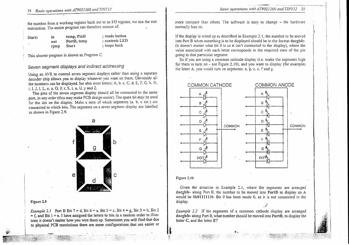
connected to which bits. The segments on a seven segment display are labelled
as shown in Figure 2.9.
a
|Figure 2.9
!
j
Example 2J Port B Bit 7 - d, Bit 6 = a, Bit 5 = c, Bit 4 = g, Bit 3 •« b. Bit 2
! = f, and Bit 1 — e. I have assigned the letters to bits in a random order to illus-
trate it doesn’t matter how you wire them up. Sometimes you will find that due
to physical PCB restrictions there are some configurations .that are easier or
Basic operations with AT90S1200 and TINY12 35
more compact than others. The software is easy to change - the hardware
normally less so.
If the display is wired up as described in Example 2.1, the number to be moved
into Port B when something is to be displayed should be in the format dacgbfe-
(it doesn’t matter what bit 0 is as it isn’t connected to the display), where the
value associated with each letter corresponds to the required state of the pin
going to that particular segment.
So if you are using a common cathode display (i.e. make the segments high
for them to turn on - see Figure 2.10), and you want to display (for example)
the letter A. you would turn on segments: a, 1?, c, e. f and g.
COMMON CATHODE COMMON ANODE
Figure 2.10
Given the situation in Example 2.1, where the segments are arranged
dacgbfe- along Port B, the number to be moved into PortB to display an Awould be ObOllllllG. Bit O' has been made 0, as it is not connected to the
display.
JExample 2.2 If the segments of a common cathode display are arranged
dacgbfe- along Port B, what number should be moved into PortB, to display the
letter C, and the letter E?
36 Basic operations with AT9US1200 and Tli\ ) 12
The letter C requires segments a, d, e and f. so the number to be moved into Port
B would be Ob 11 0001 10. The letter E requires segments a, d. e, f and g so the
number to be moved into Port B would be Obi 10101 10.
EXERCISE 2.3 If the segments are arranged abcdefg- along Port B, what
number should be moved into PortB to display the numbers 0, 1, 2, 3. 4, 5, 6,
7, 8, 9, A, b, c, d, E and F.
The process of converting a number into a seven segment code can be carried
out in various ways, but by far the simplest involves using a look-up table. The
key idea behind a look-up table is indirect addressing. So far we have been
dealing with direct addressing, i.e. if we want to read a number from register
number 4, we simply read register number 4. Indirect addressing involves
reading a number from register number X. where X is given in a different
register, called Z (the 2-bvte register spread over R30 and R31).
It’s a bit like sending a letter, where the letter is the contents of a working
register (R0-R31 ), and the address is given by the number in Z.
Example 2.3 Move the number 00 into working registers numbers R0 to R29.
Rather than writing:
clr R0 : clears R0clr Rl : clears Rl
clr R2 ; clears R2
etc.
clr R29 : clears R29
we can use indirect addressing to complete the job in fewer lines. The first
address we want to write to is R0 (address 0), so we should move 00 into Z(making 0 the address on the letter). Z. remember, is spread over both ZL and
ZH (the higher and lower bytes of Z), so we need to clear them both:
dr ZL ; clears ZLdr . ZH ;
dears ZH
We then need to set up a register with the number 0 so we can send it ‘by post'
to the other registers. We already have a register with a 0 (ZH), so we will use
that.
tfasic operations with AJ~9(fS720u aim
st ZH, Z ;
sends the number in ZH (0) to the address given by Z (also 0), and so effec-
tively clears R0. We now want to clear Rl, and so we simply increment Z to
point to address 01 (i.e. Rl). The program then loops back to cycle through all
the registers, clearing them all in far fewer lines that if we were using direct
addressing. All we need to do is test to see when ZL reaches 30, as this is past
the highest address we wish to clear.
How do we tell when ZL reaches 30? We subtract 30 from it and see whetheror not the result is zero. IfZL is 30. then when we subtract 30 from it the result
will be 0. We don’t want to actually subtract 30 from ZL. or it will start goingbackwards fast! Instead we use one of the compare instructions:
cp register, register ;
This ‘compares’ the number in one register with that in another (actually
subtracts one register from the other whilst leaving both unchanged). We thenneed to see if the result is zero. Wc can do this by looking at the zero (lag. Therearc a number of flags held in the SREG register (S3F). these are automaticallyset and cleared depending on the result of certain operations. The zero flag is
set when the result of an operation is zero. There arc two wavs to test ’the zeroHag:
brbs label, bit ;
This branches to another part of the program if a bit in SREG is set (the zeroflag is bit 1. and so bit would have to be a 1 ). Note that the label has to be within63 instructions of the original instruction. Similarly.
brbe label, bit ;
This branches to another part of the program if a bit in SREG is clear. Here is
where some of the instruction redundancy comes in. because as well as this
general instruction for testing a bit in SREG, each bit has its own particularinstruction. In this case, for the zero flag:
breq label;
which stands for branch if equal (more specifically, branch if the zero flag is
set). The opposite of this is: *.
’
^
brne label
which stands for branch if not equal (more specifically, branch if the zero flag
mm
38 Basic operations with AT90S1200 and TINY12
is clear). The complete set of redundant/non-critical instruction's is shown in
Appendix C, along with their equivalent instructions. To compare a register
with a number (rather than another register), we use the instruction:
cpi register, number ;
Please note that this only works on registers RJ6-R3J
.
but as ZL is R30 we are
all right. The complete set of instructions to clear registers RO to R29 is there-
fore:
clr ZL ;clears ZL
dr ZH ; clears ZHClearLoop: st ZH, Z : clears indirect address
inc ZL ;moves on to next address
cpi ZL, 30 ; compares ZL with 30
brne >. •‘arLoop ; branches to ClearLoop if ZL ^ 30
This six line instruction set is useful to put in the Init subroutine to systemat-
ically clear a large number of file registers. You can adjust the starting and
finishing addresses by changing the initial value of ZL and the final value you
are testing for: note, however, that you don't want to clear ZL.in the loop (i.e.
don't go past 30) because otherwise you will be stuck in an endless loop (think
about it).
exercise 2.4 Challenge! What six lines will write a 0 to RO, a 1 to Rl. a 2 to
R2 etc. all the way to a 15 to R 15?
As well as writing indirectly, we can also read indirectly:
Id register, Z . ;
This indirectly loads into register the value at the address pointed to by Z. Wetherefore have a table of numbers kept in a set of consecutive memory
addresses, and by varying Z we can read off different values. Say for example.
we keep the codes for the seven segment digits 0-9 in working registers
R20-R29. We then move 20 into Z (to ‘zero’ it to point at the bottom of the
table) and then add the number we wish to convert to Z. Reading indirectly into
temp we then get the seven segment code for that number:
Idi ZL, 20 ; zeros ZL to R20add ZL, digit ; adds digit to ZLId temp, Z ; reads Rx into temp
out PortB, temp ; outputs temp to Port B
j^The-above code translates the number in digit into a- seven segment code which
Basic operations with AT90S1200 and TINY12 39
is then outputted through Port B. Note that you will have to write the code tothe registers in the first place:coae t0
R20, Obi 1 1111 00R21, ObOllOOOOO
; code for 0
; code for 1
ldi R29, ObllllOllO; code for 9
Note that using working registers for this purpose is unusual and indeedwasteful but as there is no other SRAM on the 1200 we have no' choice Onother chips that do have SRAM, we can' use that for look-uptablesFurthermore, on other chips there is also an instruction 1pm, which alUs^outo use the Program Memory for look-up tables as well. More on this ir/theLogic Gate Simulator project on page 67.S m th
Programs D and E: counter
• Testing inputs
• Seven segment displays
Our next project will be a counter. It will count the number of times a nuchbutton is pressed from 0 to 9. After 10 counts (when it nasses 9)T ^
pUsh
should reset. The seven segment display will be connected to pins PBOto PbTand the push button will go to PD0. Figure 2.1 1 shows thecST!particular attention to how the outputs to the seven sepm^nt Hie 1
’ ^ ^
arranged. The flowchart is shown in Figure 2.12.w ^ ^ are
You can write the lnit section yourself, remembering the mill im nn tu* ubutton. Start PortB with the code for a 0 on the d^lly WeZTregis^r called Counter to keep track of thethe declarations section as R17. The reason we have assigned it R17 is that asyou may remember, registers Rl^-R31 are the ‘executive assistants’ -1^powerful registers capable of a wider range of operations. We therefore tend tofill up registers from R16 upwards, and then use R0-R15 if we run out In theInit section, set up registers R20 to R29 to hold the seven seoment J! ?numbers 0 to 9. (HINT: If you do this before setting up PortB^ou can move
fnhsecdom)”t°^ t0 mUialize iu Also remember to clear Counter in the
EXERCISE 2.5 What three lines will test the push button^oop back and test it
Then we need to see whether Counter has exceeded 9. We use cm mI
brae ,o -“.syawMs. co-JESSill®
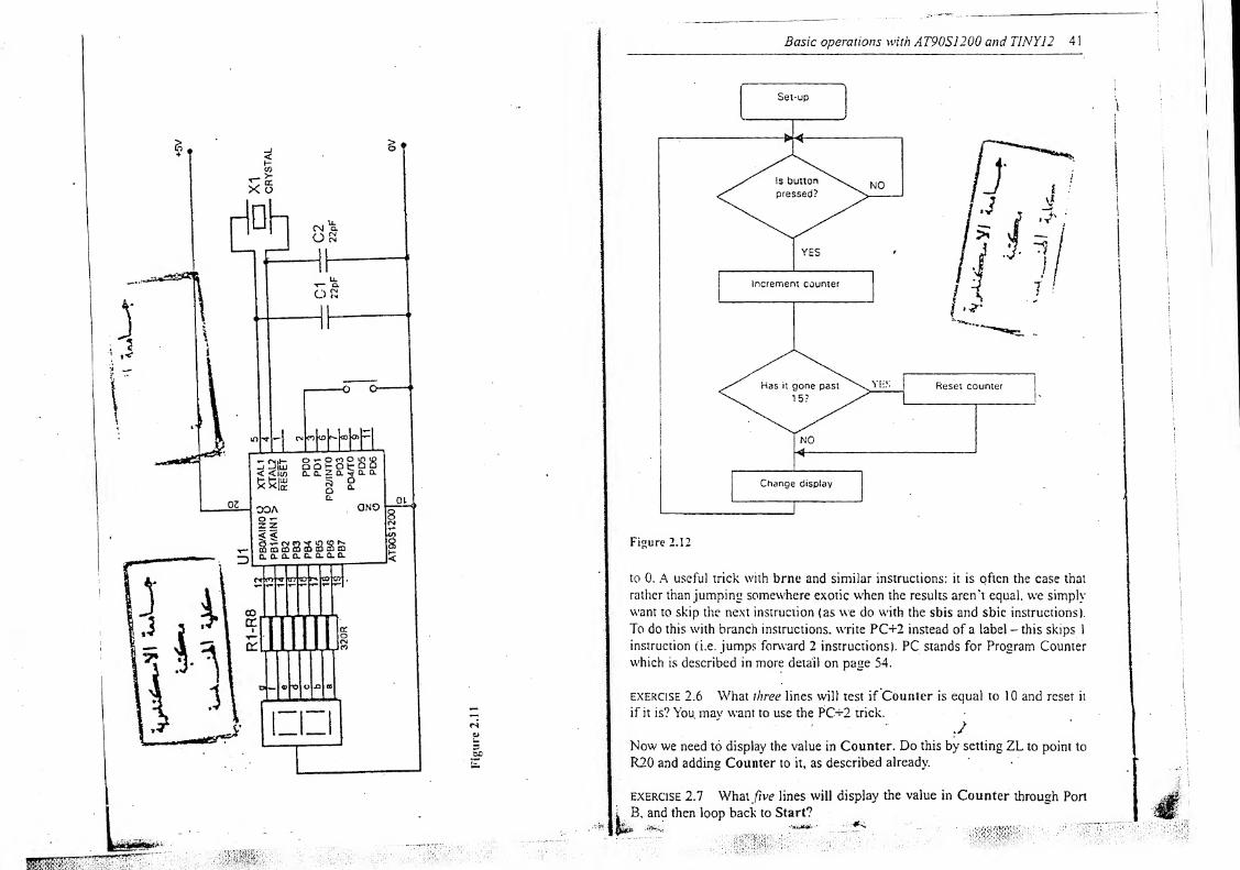
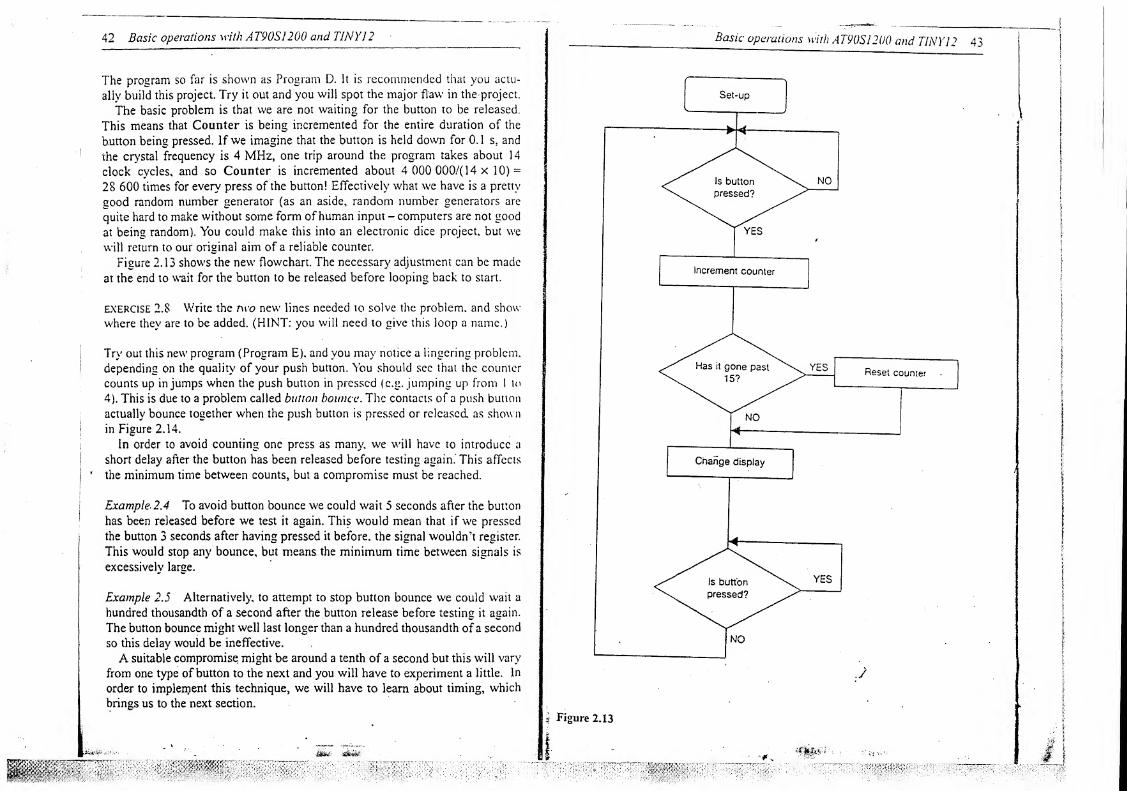
42 Basic operations with AT90S1200 and TINY12
The program so far is shown as Program D. It is recommended that you actu-
ally build this project. Try it out and you will spot the major flaw in the project.
The basic problem is that we are not waiting for the button to be released.
This means that Counter is being incremented for the entire duration of the
button being pressed. If we imagine that the button is held down for 0.1 s, and
the crystal frequency is 4 MHz, one trip around the program takes about 14
clock cycles, and so Counter is incremented about 4 000 000/(14 x 10) =
28 600 times for every press of the button! Effectively what we have is a pretty
good random number generator (as an aside, random number generators are
quite hard to make without some form ofhuman input - computers are not good
at being random). You could make this into an electronic dice project, but we
will return to our original aim of a reliable counter.
Figure 2.13 shows the new flowchart. The necessary adjustment can be made
at the end to wait for the button to be released before looping back to start.
EXERCISE 2.8 Write the two new lines needed to solve the problem, and show
where they are to be added, (HINT: you will need to give this loop a name.)
Try out this new program (Program E), and you may notice a lingering problem,
depending on the quality of your push button. You should sec that the counter
counts up in jumps when the push button in pressed (e.g. jumping up from 1 to
4). This is due to a problem called button bounce. The contacts of a push button
actually bounce together when the push button is pressed or released, as show n
in Figure 2.14.
in order to avoid couniing one press as many, we will have to introduce a
short delay after the button has been released before testing again.' This affects
' the minimum time between counts, but a compromise must be reached.
Example. 2.4 To avoid button bounce we could wait 5 seconds after the button
has been released before we test it again. This would mean that if we pressed
the button 3 seconds after having pressed it before, the signal wouldn’t register.
This would stop any bounce, but means, the minimum time between signals is
excessively large.
Example 2.5 Alternatively, to attempt to stop button bounce we could wait a
hundred thousandth of a second after the button release before testing it again.
The button bounce might well last longer than a hundred thousandth of a second
so this delay would be ineffective.
A suitable compromise might be around a tenth of a second but this will vary
from one type of button to the next and you will have to experiment a little. In
order to implement this technique, we will have to learn about timing, which
brings us to the next section.
..
‘
-&&&
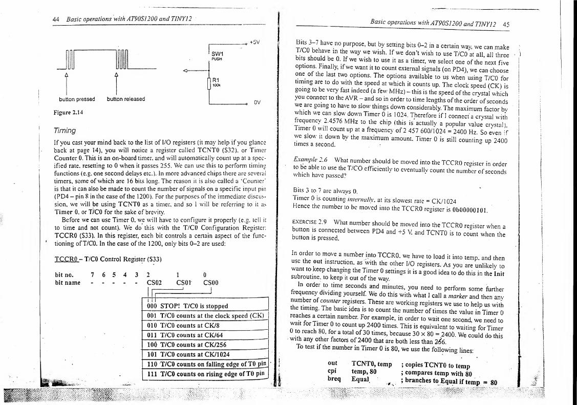
44 Basic operations with AT90S1200 and TINY]
2
Figure 2.14
Timing
If you cast your mind back to the list of I/O registers (it may help if you glance
back at page 14), you will notice a register called TCNTO (S32). or Timer
Counter 0. This is an on-board timer, and will automatically count up at a spec-
ified rate, resetting to 0 when it passes 255. We can use this to perform timing
functions (e.g. one second delays etc.). In more advanced chips there are several
timers, some of which are 16 bits long. The reason it is also called a ‘Counter’
is that it can also be made to count the number of signals on a specific input pin
(PD4 - pin 8 in the case of the 1200). For the purposes of the immediate discus-
sion, we will be using TCNTO as a timer, and so 1 will be referring to it as
Timer 0. or T/CO for the sake of brevity.
Before we can use Timer 0, we will have to configure it properly (e.g. tell it
to time and not count). We do this with the T/C0 Configuration Register:
TCCR0 (S33). In this register, each bit controls a certain aspect of the func-r
tioning ofT/C0. In the case of the 1200, only bits 0-2 are used:
TCCRO - T/C0 Control Register ($33)
bit no. 7 6 5 4 3 2 1 0
bit name CS02 CS01’ CS00
000 STOP! T/C0 is stopped
001 T/C0 counts at the clock speed (CK)
010 T/C0 counts at CK/8_
~011 T/CO counts at CK/64
100 T/CO counts at CK/256 _
101 T/C0 counts at CK/1024
110 T/CO counts on falling edge ofTO pin
111 T/CO counts on rising edge ofTO pin
Basic operations with AT90S1200 and TINY12
r^n3
K7
u
haVe-
n(TrP°Se ’bU ‘ by SCttlnS bits 0-2 a certain way. we can make
i/CO behave m the way we wish. If we don’t wish to use T/CO at all, all threeits should be 0. If we wish to use it as a timer, we select one of the next five
options Finally, ifwe want it to count external signals (on PD4), we can chooseone of the last two options. The options available to us when using T/CO fortiming are to do with the speed at which it counts up. The clock speed (CK) isgoing to be very fast indeed (a few MHz) - this is the speed of the crvstal whichyou connect to the AVR - and so in order to time lengths of the orderof secondswe are going to have to slow things down considerably. The maximum factor bvwhich we can slow down Timer 0 is 1024. Therefore if I connect' a crystal withrequenc) o MHz to the chip (this is actually a popular value crvstal)limer 0 will count up at a frequency of 2 457 600/1024 = 2400 Hz. So even ifwe slow it down by the maximum amount. Timer 0 is still countin" up 9400times a second. •
c H
ExZmp
ifx
16 What number should bc moved into the TCCRO register in orderto be able to use the T/CO efficiently to eventually count the number of secondswhich have passed?
Bits 3 to 7 are always 0.
Timer 0 is counting internally, at its slowest rate = CK/1024Hence the number to bc moved into the TCCRO register is ObOOOOOl 01.
exercise 2.9 What number should be moved into the TCCRO register when abutton is connected between PD4 and +5 V. and TCNTO is to count when thebutton is pressed.
n order to move a number into TCCRO. we have to load it into temp, and thenuse he out instruction, as with the other I/O registers. As vou are unlikely to
;Xoutf„ee
to
C
Jang,nS thC T
rTr ° SeRingS U is 3 §00d idea to d<> this in the Init
subroutine, to keep it out of the wav.
fJ"?nrber
,
t0
?me second
fand minutes, you need to perform some further
frequency dividing yourself. We do this with what I call a marker and then anvnumber of counter registers. These are working registers we use to help us withimmg. The basic idea is to count the number of times the value in Timer 0reaches a certain number. For example, in order to wait one second, we need to
D t
* °r
I'srw0 t0 C°U
?t UP 2400 tlrnes ' This is ec
luivalent to waiting for Timer0 to reach 80, for a total of30 times, because 30 x 80 = 2400. We could do thiswith any other factors of2400 that are both less than 2^6.
To test if the number in Timer 0 is 80, we use the following lines:
TCNTO, temptemp, 80
Equal,
; copies TCNTO to temp; compares temp with 80; branches to Equal if temp
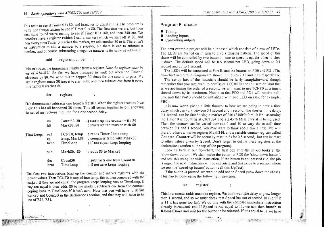
4-6 Basic operations with AT90S1200 and TIN ) 12 __
This tests to see ifTimer 0 is 80, and branches to Equal if it is. The problem is
.ve’re not always testing to see ifTimer 0 is 80. The first time we are, but then
lext time round we’re "testing to see if Timer 0 is 160, and then 240 etc. We
herefore have a register (which I call a marker) which we start off at 80, and
hen every time Timer 0 reaches the marker, we add another 80 to it. There isn’t
m instruction to add a number to a register, but there is one to subtract a
number, and of course subtracting a negative number is the same as adding it.
subi register, number ;
This subtracts the immediate number from a register. Note the register must be
me of R16-R31. So far, we have managed to work out when the Timer 0
Advances by 80. We need this to happen 30 times for one second to pass. We
ake a register, move 30 into it to start with, and then subtract one from it every
ime Timer 0 reaches 80.
dec register ;
This decrements (subtracts one from) a register. When the register reaches 0 we
;now this has all happened 30 times. This all comes together below, showing
he set of instructions required for a one second delay.
ldi Count30,30 . ; starts up the counter with 30
ldi Mark80, 80 ; starts up the marker with 80
out TCNT0, temp ; reads Timer 0 into temp
cp temp, Mark80 compares temp with Mark80
brne TimeLoop ; if not equal keeps looping
subi MarkSO, -80 •; adds 80 to Mark80
dec Count30 ; subtracts one from CounGObrne TimeLoop ;
if not zero keeps looping
The first two instructions load up the counter and marker registers with the
correct values. Then TCNT0 is copied into temp, this is then compared with the
marker. If they are not equal, the program keeps looping back to TimeLoop. If
rhey.are equal it then adds 80 to the marker, subtracts one from the counter,
.ooping back to TimeLoop if it isn’t zero. Note that you will have to define
Vlark80 and Count30 in the declarations section, and that they will have to be
me of R16-R31.
Basic operations with ATMS1200 and TINY12
Program F: chaser
0 Timing,
• Reading inputs
0 Controlling outputs
The next example project will be a ‘chaser’ which consists of a row of LEDs.
The LEDs are turned on in turn to give a chasing pattern. The speed of this
chase will be controlled by two buttons - one to speed it up, the other to slow
it down. The default speed will be 0.5 second per LED, going down to 0.1
second and up to 1 second.
The LEDs will be connected to Port B. and the buttons to PD0 and PD 1. The
flowchart and circuit diagram are shown in Figures 2.15 and 2.16 respectively.
The set-up box of the flowchart should be fairly straightforward, though
remember that you may want to configure TCCR0 in the lnit section, and that
as we are timing the order of a second, we will want to use TCNT0 as a timer,
slowed down by its maximum. Note also that PD0 and PD1 will require pull-
ups. and that PortB should be initialized with one LED on (say. for example,
PB0).
It is now worth giving a little thought to how we are going to have a time
delay which can vary between 0. 1 second and 1 second. The shortest time delay.
0.1 second, can be timed using a marker of 240 (2400/240 = 10 Hz), assuming
the Timer 0 is counting at CK/1024 and a 2.4576 MHz crystal is being used.
Then the counter can be varied between 1 and 10 to vary the overall time
between 0.1 and 1 second. You may want to think about this a little. We' will
therefore have a marker register Mark240, and a variable counter register called
Counter. Counter will be normally reset to 5 (for 0.5 second), but can be reset
to other values given by Speed. Don’t forget to define these registers at the
declarations section at the top of the program).
Looking back at our flowchart, the first box after the set-up looks at the
‘slow-down button'. We shall make the button at PD0 the ‘slow-down button’,
and test this using the sbic instruction. If the button is not pressed (i.e. the pin
is high), the next instruction will be executed and this skips to a section where
we test the ‘speed-up button’ button (call this UpTest).
If the button is pressed we want to add one to Speed (slow down the chase).
This can be done using the following instruction:
inc register ;
This increments (adds one to) a register. We don’t want life delay to grow longer
than 1 second and so we must check that Speed has not exceeded 10 (i.e. if it
is 1 1 it has gone too far). We do this with the compare immediate instruction
already introduced cpi. If Speed is not equal to 11, we can then branch to
ReleaseDown and wait for the button to be released. If it is equal to 1 1 we have
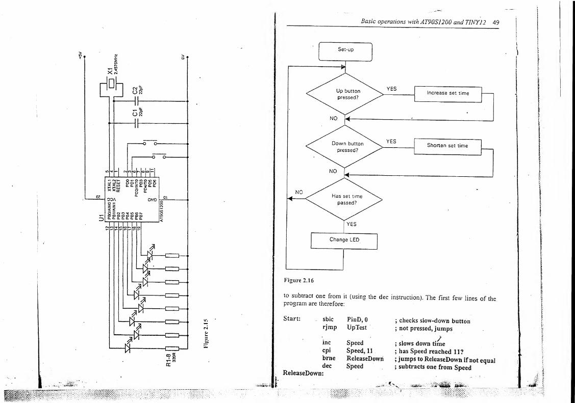
Basic operations with AT90S1200 and TINY11
Figure 2.16
to subtract one from it (using the dec instruction). The first few lines of theprogram are therefore:
Start: . sbic PinD, 0
rjmp UpTest
inc Speed
cpi Speed, 11
brne ReleaseDowii
dec SpeedReleaseDown:
; checks slow-down button
; not pressed, jumps
; slows down time
; has Speed reached 11?
; jumps to ReleaseDowii if not equal
; subtracts one from Speed
'x. £ segttf
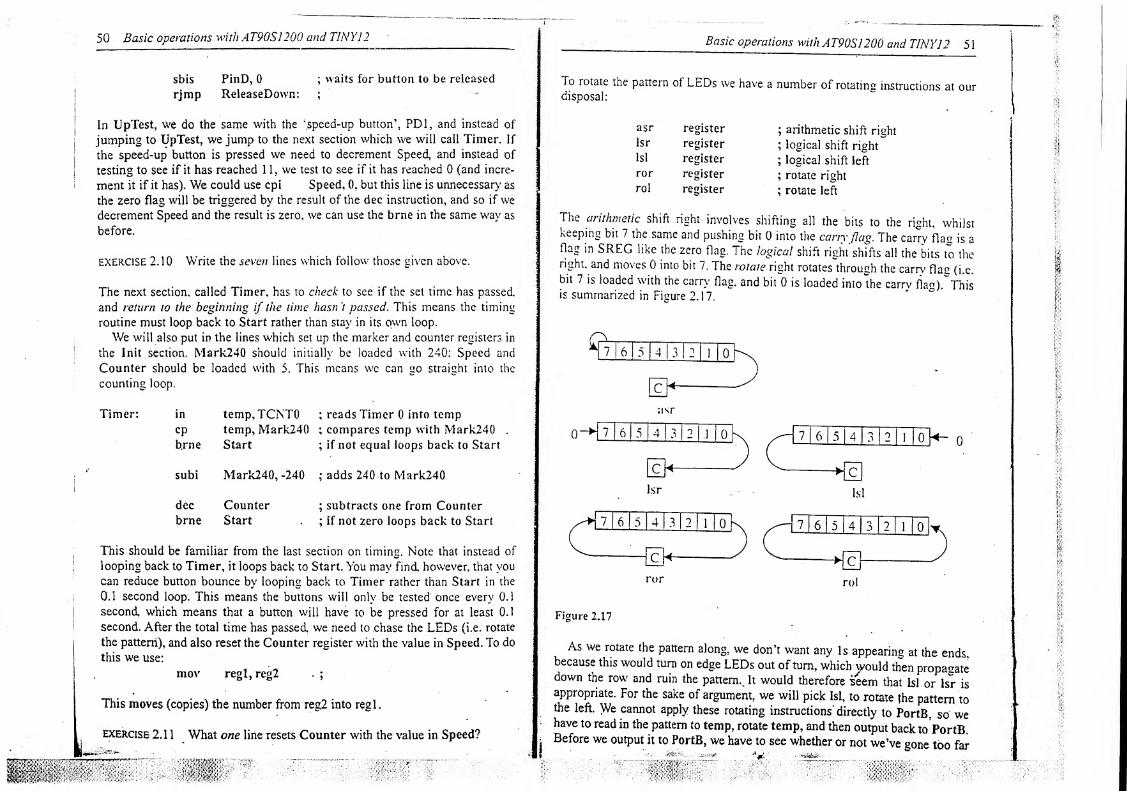
50 Basic operations with AT90SJ200 and TINY12
sbis PinD, 0 ;waits for button to be released
rjmp ReleaseDovvn; ;
In UpTest, we do the same with the ‘speed-up button’, PD I, and instead of
jumping to UpTest, we jump to the next section which we will call Timer. If
the speed-up button is pressed we need to decrement Speed, and instead of
testing to see if it has reached 1 1, we test to see if it has reached 0 (and incre-
ment it if it has). We could use cpi Speed, 0. but this line is unnecessary as
the zero flag will be triggered by the result of the dec instruction, and so if we
decrement Speed and the result is zero, we can use the brne in the same way as
before.
EXERCISE 2.10 Write the seven lines which follow those given above.
The next section, called Timer, has to check to see if the set time has passed
and return to the beginning if the time hasn V passed. This means the timing
routine must loop back to Start rather than stay in its own loop.
We will also put in the lines which set up the marker and counter registers in
the Init section. Mark240 should initially be loaded with 240; Speed and
Counter should be loaded with 5. This means we can go straight into the
counting loop.
Timer: in temp,TCNT0 ; reads Timer 0 into temp
cp temp, Mark240 ; compares temp with Mark240 .
b.rne Start ; if not equal loops back to Start
subi Mark240, -240 ; adds 240 to Mark240
dec Counter ; subtracts one from Counter
brne Start . ; if not zero loops back to Start
This should be familiar from the last section on timing. Note that instead of
looping back to Timer, it loops back to Start. You may find, however, that you
can reduce button bounce by looping back to Timer rather than Start in the
0.1 second loop. This means the buttons will only be tested once every 0.1
second, which means that a button will have to be pressed for at least 0.1
second. After the total time has passed, we need to .chase the LEDs (i.e. rotate
the pattern), and also reset the Counter register with the value in Speed. To do
this we use:
mov regl,reg2 . ;
This moves (copies) the number from reg2 into regl
.
exercise 2.1 1 What one line resets Counter with the value in Speed?
§!§!§; ||
• Basic operations with AT90SJ200 and TINY12 5
1
To rotate the pattern of LEDs we have a number of rotating instructions at ourdisposal:
The arithmetic shift right involves shifting all the bits to the right, whilstkeeping bit 7 the same and pushing bit 0 into the cany flag. The carry flau is aflag in SREG like the zero flag. The logical shift right* shifts all the bits to theright, and moves 0 into bit 7. The rotate right rotates through the carry flas (i.e.
bit 7 is loaded with the carry' flag, and bit 0 is loaded into the cany' flacJ.^Thisis summarized in Fisrure 2.17.
7 6 5 4 3 2!
6 5 4 3 2 1.1 0j
7 6 5 4 3 2 1 0|
7 16 I 5 1 4 1 3 2 10 71615 U 3 2 j 0
Figure 2.17
As we rotate the pattern along, we don’t want any Is appearing at the ends,because this would turn on edge LEDs out of turn, which would then propagatedown the row and ruin the pattern.. It would therefore seem that lsl or Isr isappropriate. For the sake of argument, we will pick lsl, to rotate {he pattern tothe left. We cannot apply these rotating instructions' directly to PortB, so wehave to read in the pattern to temp, rotate temp, and then output back to PortB.Before we output it to PortB, we have to see whether or not we’ve gone too far
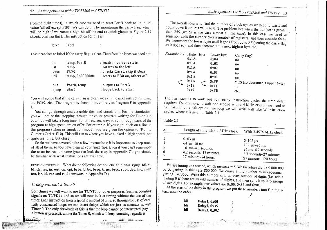
52 Basic operations with AT90S1200 and TINYJ2
(rotated eight times), in which case we need to reset PortB back to its initial
value (all off except PBO). We can do this by monitoring the carry flag, which
will be high if we rotate a high bit off the end (a quick glance at Figure 2.17
should confirm this). The instruction for this is:
brcc label ;
This branches to label if the carry flag is clear. Therefore the lines we need are:
in temp, PortB ; reads in current state
lsl temp ; rotates to the left
brcc PC+2 ; checks Carry, skip if dear
ldi temp, ObOOOOOOOl ; resets to PBO on, others off
out PortB, temp ; outputs to PortB
rjmp Start ; loops back to Start
You will notice that if the carry flag is dear, we skip the next instruction using
the PC+2 trick. The program is shown in its entirety as Program F in Appendix
J.
You can go through and assemble this, and simulate it. For the- simulation,
you will notice that stepping through the entire program waiting for Timer 0 to
count up will take a long time. For this reason, ways to run through parts of the
program at high speed are on offer. For example, if you right click on a line in
the program (when in simulation mode), you are given the option to ‘Run to
Cursor' (Ctrl + F10). This will run to where you have clicked at high speed (not
quite real time, but close).
So far we have covered quite a few instructions; it is important to keep track
of all of them, so you have them at your fingertips. Even if you can’t remember
the exact instruction name (you can look these up in Appendix C), you should
be familiar with what instructions are available.
revision EXERCISE What do the following do: sbi, cbi, sbic, sbis, rjmp, ldi, st.
Id, clr, sen in, out, cp. cpi, brbs, brbe, breq, brne. brcc, subi, dec, inc, mov,
asr, lsr, lsl, ror and rol? (Answers in Appendix D.)
Timing without a timer?
Sometimes we will want to use the TCNTO for other purposes (such as counting
signals on T0/PD4), and so we will now look at timing without the use of this
timer. Each instruction takes a specific amount oftime, so through the use ofcare-
fully constructed loops we can insert delays which are just as accurate as with
Timer 0. The only drawback of this is that the loop cannot be interrupted (say, if]
a button is pressed), unlike the Timer 0, which will keep counting regardless.
Basic operations with
A
T90S1200 and TINY12 53
The overall idea is to find the number of clock cycles we need to waste andcount down from this value to 0. The problem lies when the number is greaterthan 2oo (which is the case almost all the time). In this case we need tosomehow split the number over a number of registers, and then cascade them.We decrement the lowest byte until it goes from 00 to FF (setting the carry fla°as it does so), and then decrement the next highest byte etc.
Example 2.
7
Higher byte Lower byte
OxlA 0x04OxlA 0x03OxlA 0x02OxlA 0x01
OxlA 0x00OxlA OxFF0x19 OxFF0x19 OxFE
Carry flag?
YES (so decrements upper byte)
The first step is to work out how many instruction cvcles the time delavreqmres. For example, to wait one second with a 4 MHz crystal, we need tokill 4 million clock cycles. The loop we will write will take \v' instructioncycles, where ,v is given in Table 2.1.
Table 2.1
f Len"th of time with 4 MHz clock With 2.4576 MHz clock
0-63 pis
64 pis— 16 ms16 ms-4.1 seconds
4.2 seconds- 17 minutes1 7 minutes-74 hours
0-102 ps
102 jis-26 ms26 ms-6.7 seconds
6.7 seconds-27 minutes27 minutes-] 20 hours
We are timing one second, which means jr = 5. We therefore divide 4 000 000) cutting in this case 800 000. We convert this number to hexadecimal
getting 0xC3500. Write this number with an even number of digits (i e add a
ofrtn=.° lfth5e are an odd number of digits), and then split it up into groupsof two digits. For example, our values are 0x00, 0x35 and 0x00
P
dd“y " the
P
'°8ram W' P“ n“mbErei"“ fi>= regis-
Delayl, 0x00Delay2, 0x35
Delay3, OxOC
mmm
54 Basic operations with AT90S1200 and TINY12
The delay itself consists ofjust one line per delay register plus one at the end
(i.e. in our case four lines). To help us achieve such a short loop we need to use
a new instruction:
sbci reg, number ;
Subtract the immediate number from a register, and also subtract 1 if the carry
flag is set. For example:
sbci Delay2, 0 ;
This effectively subtracts 1 from Delay 2 if the carry flag is set, and subtracts 0
otherwise. Our delay loop is as follows:
Loop: subi Delavl, 1 ; subtracts 1 from Delavl
sbci Delav2, 0 ; subtracts 1 from Delay! if Carry is set
sbci Delay3, 0 ; subtracts 1 from Deiav3 if Carry is set
brcc Loop ; loops back if Carry is clear
When it finally skips out of the loop, one second will have passed. The first
thing to note is that the length of the loop is five clock cycles (the branching
instruction takes ftvo clock cycles). You can now see where the numbers in Table
2. 1 come from - for every extra delay register you add there is an extra cycle in
the loop. The reason we have used subi to subtract 1 instead of dec is that unlike
subi, dec doesn’t affect the carry flag. We clearly rely on the carry flag in order
to know when to subtract from the higher bytes, and when to skip out of the
/loop.
The program counter and subroutines
There is an inbuilt counter, called the program counter, which tells the AVRwhat instruction to execute next. For normal instructions, the program counter
(or PC for short) is simply incremented to point to the next instruction in the
program. For an rjmp or brne type instruction, the number in the PC is changed
so that the AVR will skip to somewhere else in the program.
Example 2.8
Start:
039 sbi PortB, 0 ; turns on LED03A sbic PinD, 0 ; tests push button
03B cbi PortB, 0 ; turns off LED
•
Ijl!jlffi V’
Basic operations with AT90S1200 and TINY]
2
55
Loop:
03C’ dec Counter
03D breq PC+203E rjmp Start
03F rjmp Loop
skips next line if 0
The above example segment has the program memory addresses for each
instruction on the left-hand side in hexadecimal. Note that blank lines aren’t
given addresses, nor are labels, for they are actually labelling the address that
follows. Looking at the behaviour of the PC in the above, it starts at 039 andupon completion of the sbi instruction gets incremented to 03A. Then PinD, 0
is tested. If it is high, the PC is simply incremented to 03B. but if it is low, the
program skips, i.e. the PC is incremented twice to 03C. The rjmp Start
instruction moves 039 into the PC, making the program skip back to Start. Thisalso sheds some light on the PC+2 trick we've used a few times already, if the
result is *not equal’ (i.e. zero flag clear), the program adds 2 to the PC rather
than 1, thus skipping one instruction.
exercise 2.12 In the example above, what is the effect of the instruction
rjmp Loop on the PC?
This now brings us to the topic of subroutines. A subroutine is a set ofinstructions within the program which you can access from anywhere in the
program. When the subroutine is finished, the program returns and carries onwhere it left off. The key feature here is the fact that the chip has to
remember where it was when it called the subroutine so that it can knowwhere to carry on from when it returns from the subroutine. This memory is
kept in what is known as a stack. You can think of the stack as a stack ofpapers, so when the subroutine is called the number in the program counteris placed on top of the stack. When a returning instruction is reached the topnumber on the stack is placed back in the program counter, thus the AVRreturns to execute the instruction after the one that called the subroutine. The1200 has a three level stack. When a subroutine is called within a subroutine,
the number in the PC is placed on top of the stack, pushing the previousnumber to the level below. The subsequent returning instruction will, as
always, select the number on the top of the stack and put it into the PC. Athree level stack means you can call a subroutine within a subroutine withina subroutine, but not a subroutine within a subroutine within a subroutinewithin a subroutine. This is because once you’ve pushed three values on to
the stack, and you call another subroutine, hence pushing another value on to
the stack, the bottom of the stack is lost permanently. The example in Figure2.18 illustrates this problem.
e
.'.WWM
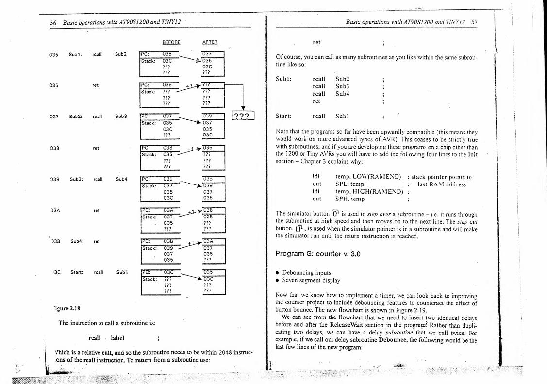
56 Basic operations with AT90S1200 and TINY12
The instruction to call a subroutine is:
Vhich is a relative call, and so the subroutine needs to be within 2048 instruc-
ons of the rcall instruction. To return from a subroutine use:
Basic operations with AT90S1200 and TINY1
2
57
Of course, you can call as many subroutines as you like within the same subrou-
tine like so:
Subl: rcall Sub2
rcall Sub3
rcall Sub4
ret
Start: rcall Subl
Note that the programs so far have been upwardly compatible (this means they
would work on more advanced types of AVR). This ceases to be strictly true
with subroutines, and if you are developing these programs on a chip other than
the 1200 or Tiny AVRs you will have to add the following four lines to the Init
section - Chapter 3 explains why:
!di temp, LOW(RAMEND) ; stack pointer points to
out SPL, temp; last RAM address
ldi temp, HICH(RAMEND);
out SPH, temp;
The simulator button IP is used to step over a subroutine - i.e. it runs through
the subroutine at high speed and then moves on to the next line. The step out
button, (P , is used when the simulator pointer is in a subroutine and will makethe simulator run until the return instruction is reached.
Program G: counter v. 3.0
• Debouncing inputs
• Seven segment display
Now that we know how to implement a timer, we can look back to improvingthe counter project to include debouncing features to counteract the effect ofbutton bounce. The new flowchart is shown in Figure 2.19.
We can see from the flowchart that we need to insert two identical delays
before and after the ReleaseWait section in the program? Rather than dupli-
cating two delays, we can have a delay subroutine that we call twice. Forexample, ifwe call our delay subroutine Debounce, the following would be the
last few lines of the new program:
t£\_ .. ... . ; - -r-
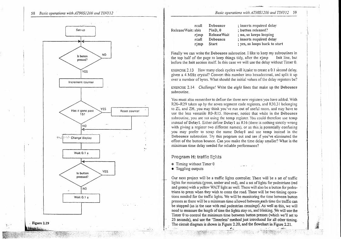
58 Basic operations with AT90S1200 and TINY12 Basic operations with XT90S1200 and TINY12 59
rcall Debounce;inserts required delay
ReleaseWait: sbis PinD, 0 ;button released?
rjmp ReleaseWait ; no, so keeps looping
real! Debounce ; inserts required delay
rjmp Start;yes, so loops back to start
Finally we can write the Debounce subroutine. I like to keep my subroutines in
the top half of the page to keep things tidy, after the rjmp Init line, but
before the init section itself. In this case we will use the delay without Timer 0.
EXERCISE 2.13 How many clock cycles will intake to create a 0. 1 second delay,
given a 4 MHz crystal? Convert this number into hexadecimal, and split it up
over a number of bytes. What should the initial values of the delay registers be?
EXERCISE 2.14 Challenge! Write the eight lines that make up the Debounce
subroutine.
You must also remember to define the three new registers you have added. With
R20-R29 taken up by the seven segment code registers, and R30.31 belonging
to ZL and ZH, you may think you’ve run out of useful room, and may have to
use the less versatile R0-R15. However, notice that while in the Debounce
subroutine, you are not using the temp register. You could therefore use temp
instead of Delay 1. Either define Delayl as R16 (there is nothing strictly wrong
with giving a register two different names), or as this.is potentially confusing
you may prefer to scrap the name Delayl and use temp instead in the
Debounce subroutine. Try this program out and see if you’ve, eliminated the
effect of the button bounce. Can you make the time delay smaller? What is the
minimum time delay needed for reliable performance?
Program H: traffic lights
© Timing without Timer 0
• Toggling outputs
Our next project will be a traffic lights controller. There will be a set of traffic
lights for motorists (green, amber and red), and a set of lights foF pedestrians (red
and green) with a yellow WAIT light as well. There will also be a button for pedes-
trians to press when they wish, to cross the road. There will be two timing opera-
tions needed for the traffic lights. We will be monitoring the time between button
presses as there will be a minimum time allowed between^ach time the traffic can
be stopped (as is the case with real pedestrian crossings). As well as this, we will
need to measure the length oftime the lights stay on, and blinking. We will use the
Timer 0 to control the minimum time between button presses (which we’ll set to
25 seconds), and use the ‘Timerless’ method just introduced for all other timing.
The circuit diagram is shown in Figure 2.20, and the flowchart in Figure 2.2 1,
62 Basic operations with AT90S1200 and TINY12
You can write the I-nit section yourself, noting that PDO requires an internal
pull-up. Set up TCNTO to count at CK/1024.
The first two lines get the LEDs in the correct state with the red pedestrian
light on, as well as the motorists’ green.
exercise 2. 1 5 What two lines will do this?
We need to perform some sort of timing during this initial loop so that while
it is waiting for the button, it can also be timing out the necessary 25 seconds.
This will be taken care of by a subroutine called Timer which we will write
later. So after these two first lines insert:
Timer ; keeps timing
i In this subroutine we will use the T bit in SREG, a temporary bit you can use!
for your own purposes. We will use it to signal to the rest of the program
whether or not the required 25 seconds have passed. It will initially be off. but
after the traffic is stopped, and the people cross etc., it is set. When it is set and
Timer is called it will count down, but rather that staying in a loop until the
time has passed it returns (using ret) if the required time hasn’t passed. Whenthe required time does pass, the T bit is cleared again, and the rest of the
program knows it's OK to stop the traffic again. After this instruction we test
the button.
exercise 2.16 What ftvo lines will then test the push button and loop back to
Start if it isn’t pressed?
^ exercise 2.17 If the button is pressed the pedestrian’s WAIT light should be
turned on, what one line does this?
To test the T bit, you can use one of the following instructions:
I
brts label ; branches if the T bit is set
brtc label ; branches if the T bit is clear
exercise 2.18 What two lines form a new loop which calls Timer, and tests
the T bit in SREG, staying in the loop until the T bit is clear.
After the required time has passed we can start slowing the traffic down. Turn
the green motorists’ light off, and the amber one on. Keep all other lights
unchanged.
EXERCISE 2.
1
9 What two lines achieve this?
As the flowchart shows, there arc quite a few time delays required and rather
Basic operations with AT90SI200 and TINY12 63
than copy the same thing over and over, it makes sense to use a time delay
subroutine. If we look at the minimum delay we will be timing (which is 0.5
second for the flashing), we can write a delay for this length and then just call
it several times to create longer delays. The delay will be called HalfSecond,
and so to wait 4 seconds we call this subroutine 8 times. We could simply write
rcail HalfSecond eight times, but a shorter way would be the following:
FourSeconds:
ldi temp, 8
rcail HalfSecond
dec temp
brne FourSeconds
temp is loaded with 8, and then each time it is decremented HalfSecond is
called. After doing this eight times it skips out of the loop.
After this 4 second delay the red motorists’ light must be turned on, and the
amber one off. The red pedestrian light must be turned off, and the green one
on. The pedestrian's WAIT light must also be turned off.
EXERCISE 2.20 Which two lines will make the required output changes?
exercise 2.21 Which four lines make up an 8 second delay?
After the 8 seconds, the red motorists’ light turns off, and the motorists' amberand pedestrians' green lights must flash. Start by turning the flashing lights on,
and then we will look at how to make them flash.
EXERCISE 2.22 Which Avo lines make the required output changes?
To toggle the required two lights, we need to invert the states of the bits. There
are two ways to invert bits. We could take the ones complement of a register,
using:
com register ;
This inverts the states of all of the bits in a register (0 becomes 1, 1 becomes 0).
exercise 2.23 If the number in temp is OblOHOOll, what is its resulting
value after com temp?
However, we want to selectively invert the bits. This is^done using the exclusive
OR logic command. A logic command looks at one or more bits (as its inputs)
and depending on their states produces an output bit (the result of the . logic
operation). The table showing the effect of the more common inclusive ORcommand on 2 bits (known as a truth table) is shown below:
64 Basic operations with AT90S1200 and TINY!
2
inputs result
ir 0 0
0 1 i
i 0 1
1 1 1
The output bit (result) is high if either the first or the second input bit is high
(or ifboth are high). The exclusive OR is different in that if both inputs are high,
the output is low:
inputs result
0 0 0
0 1 1
1 0 I
1 1* 0
One of the useful effects is that if the second bit is 1. the first bit is toggled, and
I if the second bit is 0. the first bit isn’t toggled (see for yourself in the table). In
this way certain bits can be selectively toggled. If wc just wanted to toggle bit 0
of a file register, we would exclusive OR the file register with the number
i 00000001."
iThe exclusive OR instruction is:
I
i
eor regl, reg2 ;
./This exclusive ORs the number in reg2 with the number in regl, leaving the
|
result in regl.
EXERCISE 2.24 What four lines will read state of the lights into temp, selec-
tively toggle bits 1 and 3, and then output temp back to PortB. (Hint: You will
need a new register, call it tog.)
exercise 2.25 Challenge
!
Incorporate the previous answer into a loop that
waits half a second, selectively toggles the correct lights, and repeats eight
times. You will need a new register to count the number of times round the loop:
call this Counter, and call the loop FlashLoop. This should take eight lines.
The traffic lights can now return to their original states, but before looping back
to Start, remember to set the T bit. You can do this directly using the following
Basic operations with AT90S1200 and TINY12 65
exercise 2.26 Write the final two lines of the program.
What remains for us now are the two subroutines, HalfSecond and Timer. Wewill tackle HalfSecond first as it should be the more straightforward.
exercise 2.27 Without using the Timer 0, create a half second delay, and use
this to write the eight lines of the HalfSecond subroutine. A 2.4576 MHzcrystal is being used.
For Timer, we first test the T bit. If it is clear we can simply return.
t
exercise .2.28 Write the first rwo lines of the Timer subroutine.
We can then use the same method we used before in timing loops; however,
instead of looping to the top of the section, return from the subroutine. The
required time is 25 seconds, which on a 2.4576 MHz crystal with Timer 0
running at CK/1024 corresponds to a marker of 240 and a counter of250 (work
it out!).
exercise 2.29 Challenge! Write the remaining ten lines of the Timer subrou-
tine. Assume your counter and marker registers have been set up in the Init
section (do this! ), and reset the counter register with its initial value at the end
of the subroutine. Don't forget to clear the T bit at the end of the subroutine (use
the clt instruction).
Congratulations! You have essentially written this whole program yourself. To
check the entire program, look at Program H (Appendix J).
Logic gates
We had a short look at the inclusive OR and exclusive OR logic gates, and nowwe’ll look at other types: AND, NAND, NOR, ENOR, BUFFER, NOT. Thetruth tables are as follows:
AND
This is useful for masking (ignoring certain bits). If the second bit is 0, the first
bit is masked (made 0). If the second bit is 1, the first bit remains intact.
inp uts result
0 0 0
0 1 0
1 0 0
1 1 1
66 Basic operations with AT90S1200 and TINY12
Therefore ANDing a register with ObOOOOl 1 1 1 masks bits 4-7 of the register,
and leaves bits 0-3 the same.
NAND
inputs result
0 0 i
0 1 i
1 0 1
1 1 0
This is the opposite ofan AND
NOR
This is the opposite ofan OR
ENOR
Basic operations with AT90S1200 and TINY12 67
There aren’t specific instructions for all these gates, but they can be imple-
mented using a combination of available instructions.
Program I: logic gate simulator
• Logic functions
m TinyAVR
Our next project will be a logic gate simulator which can be programmed to
act as any of the eight gates given above. It will therefore require two inputs
and one output, and three inputs will together^select which gate it is to emulate.
This makes a total of six I/O pins, which just fits on the Tiny AVR chips. Wewill be writing this program for the Tiny 12 AVR in particular, but it can be
adapted to most of the other types, including the 1200 that we have so far been
writing for. Figure 2.22 shows the pin layouts of some of the members of the
Tiny family.
AT liny 10/1
1
AT tiny 12
VCC
PB2 (SCK/TO)
PB1
{MISO/INTO/AIN1}
PBO (MOSI/AINO)
Figure 2.22
Basic features about this family include having a 6-bit Port B (PB0-PB5), but
these six I/O pins are available only under certain circumstances. For example,
you can see that PBS and PB4 are also the oscillator inputs, and so to use these
as I/O pins requires selection of the internal oscillator. Using a separate oscil-
lator (and therefore only needing XTALI as a clock input) means PB4 is avail-
able, but PB3 isn’t. Using the RESET pin as a reset pin means losing PB5. So
you can see that having six I/O is very much a maximum. Also, take note that
on the TinylO and Tinyl 1 PB5 is an input only . On the Tiny 12, PB5 is an input
or an output drain (this means you can make it an output/but only a low output
- i.e. it can sink but not source current). This means that although PinB and
DDRB are 6 bits long, PortB is only 5 bits long. PBS therefore has no internal
, pull-up, and so needs an external resistor. An advantage of the Tiny AVRs over
the 1200 model we have been using so far is the availability of the following
> instruction:
I" -
68 Basic operations with AT90S1200 and TINY12
lpm ;
This loads the contents of the program memory pointed to by Z into register
RO. This means we can use the program memory itself as a look-up table, as
opposed to using up working registers. It is also more efficient on code, as each
instruction in the program memory is 16 bits long, so we can store 2 bytes in
place of an instruction. We will be needing this instruction in the example
project.
Figure 2.23
The circuit diagram for the logic gate project is shown in Figure 2.23. Note
that the NOT and Buffer gates take only one input, and so we will be using PB
1
as the input for these gates. Therefore, the effective two-input truth tables for
the NOT and Buffer gates are:
i : nqi
Basic operations with AT90SJ200 and TINY12 69
Buffer
inputs result
0 0 0
0 1 0
1 0 1
1 1 1
EXERCISE 2.30 Have a go yourself at constructing the flowchart, before
looking at my version in the answer section. You need not make it more than
three boxes in size, as we aren’t yet concerned with sorting out how to manage
the imitating of the individual gate types.
When writing the Init section the output, PB2, should initially be off. To choose
which logic gate the AVR is to imitate, we have a binary switch which sets its
outputs between (000) and (111) depending on the state of the switch. We there-
fore have to use this in the program to determine which section to jump to.
Although the output from the switch is between 000 and 111. the resulting
number in PinB is between xxOOOx and xxl 1 lx. where the states of bits 0. 4
and 5 must be ignored. We therefore take the number in PinB and mask bits 0.
4 and 5 using:
andi reg, number ;
This AN Ds the number in a register with the immediate number (onlyfor regis-
ters R16-R31). To mask bits 0, 4 and 5, but keep bits 1-3 intact, we AND the
register with ObOOl 1 10. We then rotate it once to the right, making sure that
only zeros appear in bit 5 during the rotation.
EXERCISE 2.3 1 What is the appropriate rotation instruction to use?
The result is a number between 0 and 7 which we shall use to access a location
in the program memory, and so we should load PinB into the ZL register as this
will be used to point to a specific address,
EXERCISE 2.32 Write the three lines which read PinB into ZL, mask bits 0, 4
and 5, and then rotate it to the right as required.
Our look-up table will begin after the rjmp Init instruction. This instruc-
tion is at address 000 of the program memory (which is why it is the first one
executed). Instructions are 16 bits long, and so take up 2 bytes (or one word).
Program memory addresses are therefore word addresses, and the byte address
is 2 times the word address. Figure 2.24 illustrates this.
70 Basic operations with AT90S1200 and TINY12
word 00
0010 00110001 0000.
= and rl6,rl7
bvte 00 byte 01
Figure 2.24
Our look-up table will therefore start at word address 001 which is equivalent
o byte address 002. ZL points to the byte address, so we will have to add 2 to
ZL to start it pointing to the bottom of the look-up table.
Exercise 2.33 Which two lines will add 2 to ZL and then use ZL to read a
. alue from the program memory into R0?
Mow the real question is what to have in the look-up table that is going to tell
he program how to act like a particular logic gate. After some thought. 1 have
ound that using a split form of the truth table for each gate gives us the most
straightforward solution. What we are about to do now may appear tar from
ibvious, but hopefully after some thought you will see that ultimately it works
ather neatly.
We are going to have a byte for each logic gate. For each gate, we take the
ruth tableland look at the set of output states (e.g. 0001 for an AND gate, and
>11 1 for an inclusive OR). We then split these nibbles into two sets of 2 bits,
md make these bits 4 and 5 and 0 and 1 of a byte. For example, AND: 0001
plits into 00 and 01, and then becomes 00000001. Inclusive OR: 0111 splits
nto 0 1 and 1 1 , and the becomes 000 1 0Q 1 1
.
XERC1SE 2.34 What are the relevant bytes for the NAND, NOR, ENOR, EOR.
MOT and Buffer gates?
Ve then list these in the look-up table in any order we choose (noting that their
‘osition in the table defines how the code in FBI, 2 and 3 refers to a particular
rate). The assembler has directives (instructions for the assembler) which tell it
o place the following word or byte into the program memory. These directives
re .dw (define word) and .db (define byte). If using .dw, you will have to
'roup the bytes derived above into pairs (arbitrarily if you wish), e.g.:
dw ObOOOOOOOlOOOlOOll ; code for AND and IOR
msm
Basic operations with AT90S1200 and TINY]2 1 1
.db ObOOOOOOOl, ObOOOlOOll ;code for AND, code for IOR
There is one important difference between the two lines above. When using .dw,
the lower byte of the word has the lower byte address. For example, if the two
lines above were both written at word address 00, the code for the IOR would
be at byte address 00 in the .dw example, and at byte address 01 in the .db
example. As long as you take note of the correct byte addresses, it doesn’t
matter which way you do it.
EXERCISE 2.35 Complete the other three lines of the look-up table using .dw
or ,db. '
Therefore, using the 1pm instruction we have obtained a form of the truth table
for each gate at R0. We will then test Input A of the gate (PB4). If it is low we
swap the nibbles of R0 (e.g. 00000001 becomes 00010000). What this does is
select which half of the truth table we wish to access (remember we split it up
into two halves). The swap instruction is:
and swaps upper and lower nibbles of a register. We then test Input B of the gate
(PBS). If it is low we rotate the number in RO to the right. What this does is
select which of the two outputs remaining in the truth table is the right one. The
four lines we need are therefore:
sbis PinB, 4
swap R0sbis PinB, 5
ror R0
; tests Input A;swaps nibbles if low
;tests Input B
;rotates right if low
The state of R0. bit 0 now holds the output we wish to produce in PB0.
However, we don’t want to change the states of the pull-ups on the inputs, so wewant to move a number into PortB that is all 1 s for PB1-4. and PB0 equal to bit
0 of RO. Just like ANDing is a way to force certain bits low (masking), inclu-
sive ORing is a way to force certain bits high. For example, in this case if weIOR RO with Obi 1 1 10 we will get a number that is all Is except PB0 whose
state is intact. We can then move the result of this into PortB safe in the knowl-
edge that the pull-ups will remain. The inclusive OR instruction is:
./ori reg, number ;
This inclusive ORs a register with the immediate number, but only works on
registers R16-R31. We therefore have to move R0 into temp using the movinstruction.
i$;r
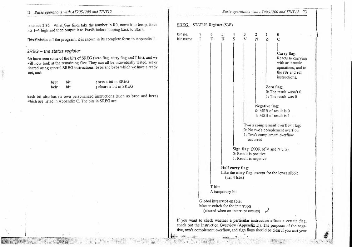
12 Basic operations with AT90S1200 and TINY12 Basic operations with AT9UB1200 and TINY12 73
iXERClSE 236 Whatfour lines take the number in RO, move it to temp, force
)its 1-4 high and then output it to PortB before looping back to Start.
This finishes off the program, it is shown in its complete form in Appendix J.
SREG - the status register
vVe have seen some of the bits ofSREG (zero flag, carry flag and T bit), and we
vvill now look at the remaining five. They can all be individually tested, set or
cleared using general SREG instructions: brbc and brbs which we have already
net, and:
bset bit ;sets a bit in SREG
bclr bit ;clears a bit in SREG
Each bit also has its own personalized instructions (such as breq and brcc)
which are listed in Appendix C. The bits in SREG are:
SREG- STATUS Register (S3F)
bit no. 7
bit name I
6 5 4 3 2 1
T H S V N Z0
C
Carry flag:
Reacts to carrying
with arithmetic
operations, and to
the ror and rol
instructions.
Zero flag:
0: The result wasn’t 0
1 : The result was 0
Negative flag:
0: MSB of result is 0
1 : MSB of result is 1
Two’s complement overflow flag:
0: No two s complement overflow
1 : Two's complement overflow-
occurred
Sign flag: (XOR ofV and N bits)
0: Result is positive
1 : Result is negative
Half carry flag:
Like the carry flag, except for the lower nibble
(i.e. 4 lsbs)
Tbit:
A temporary bit
Global interrupt enable:
Master switch for the interrupts
(cleared when an interrupt occurs)
If you want to check whether a particular instruction affects a certain flag,
check out the Instruction Overview (Appendix D). The purposes of the nega-
tive, two’s complement overflow, and sign flags should be clear if you cast your
"1S1I
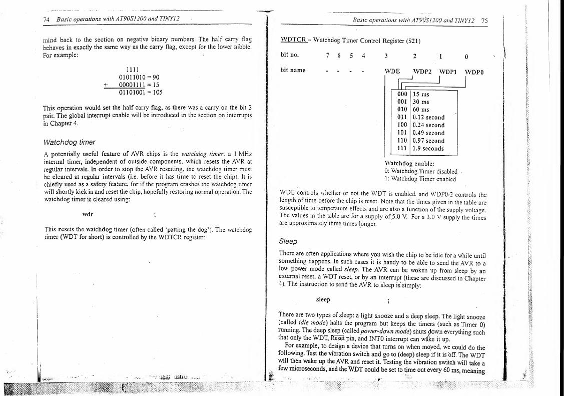
74 Basic operations with AT90S1200 and TINY12
mind back to the section on negative binary numbers. The half carry flag
behaves in exactly the same way as the carry flag, except for the lower nibble.
For example:
1111
01011010 = 90
± 00001111 = 15
01101001 = 105
This operation would set the half carry flag, as there was a carry on the bit 3
pair. The global interrupt enable will be introduced in the section on interrupts
in Chapter 4.
Watchdog timer
A potentially useful feature of AVR chips is the watchdog timer: a 1 MHzinternal timer, independent of outside components, which resets the AVR at
regular intervals. In order to stop the AVR resetting, the watchdog timer must
be cleared at regular intervals (i.e. before it has time to reset the chip). It is
chiefly used as a safety feature, for if the program crashes the watchdog timer
will shortly kick in and reset the chip, hopefully restoring normal operation. The
watchdog timer is cleared using:
wdr ;
This resets the watchdog timer (often called ‘patting the dog’). The watchdog
.timer (WDT for short) is controlled by the WDTCR register:
Basic operations with A T90S1200 and TINY12 75
WDTCR - Watchdog Timer Control Register ($21)
bit no. 7 6 5 4 3 2 1 0
bit name .... WDE WDP2 WDP1 WDP0
000 15 ms001 30 ms010 60 mson 0.12 second
100 0.24 second
101 0.49 second
110 0.97 second
111 1.9 seconds
Watchdog enable:
0: Watchdog Timer disabled
1 : Watchdog Timer enabled
WDE controls whether or not the WDT is enabled, and WDP0-2 controls thelength of time before the chip is reset. Note that the times given in the table aresusceptible to temperature effects and are also a function of the supply voltase.The values in the table are for a supply of 5.0 V. For a 3.0 V supplv the timesare approximately three times longer.
Sleep
There are often applications where you wish the chip to be idle for a while untilsomething happens. In such cases it is handy to be able to send the AVR to alow power mode called sleep. The AVR can be woken up from sleep by anexternal reset, a WDT reset, or by an interrupt (these are discussed in Chapter4). The instruction to send the AVR to sleep is simply:
sleep;
There are two types of sleep: a light snooze and a deep sleep. The light snooze(called idle mode) halts the program but keeps the timers (such as Timer 0)running. The deep sleep (calledpower-down mode) shuts down everything suchthat only the WDT, Reset pin, and INTO interrupt can w^ke it up.
For example, to design a device that turns on when moved, we could do thefollowing. Test the vibration switch and go to (deep) sleep if it is off*. The WDTwill then wake up the AVR and reset it. Testing the vibration switch will take afew microseconds, and theWDT could be set to time out every 60 ms, meaning
76 Basic operations with AT90S1200 and TINY12
the AVR is only on for about a thousandth of the time. When the vibration
switch does eventually trigger the AVR will skip the sleep instruction and
continue with normal operation. The WDT could then be disabled or reset at
regular intervals using wdr.
To control the sleep properties of the AVR, we use an I/O register called
MCUCR (S35). Bit 5 of the MCUCR is the sleep enable, and this bit must be
set ifyou wish to use the sleep instruction. Bit 4 selects which type of sleep you
require (0 for idle mode and 1 for power-down mode).
More instructions - loose ends
Through the example projects we have encountered the majority of the instruc-
tions for the 1200 and Tiny AVRs. Here is the remainder:
i
' neg reg ;
This instruction makes the number in a register negative (i.e. takes the rwos
complement).
n°p ;
This stands for no operation, in other words do nothing. This essentially wastes
one clock cycle, and can be quite useful. There are further instructions which
perform logic and arithmetic operations on pairs of registers:
and regl, reg2;ANDs regl and reg2, leaving result in regl
-or regl, reg2 ; ORs regl and reg2, leaving result in regl
add regl, reg2 ; adds regl and reg2, leaving result in regl
adc regl, reg2 ; as add, bu't adds an extra 1 if the Cam' flag is set
sub. regl, reg2 ; subtracts reg2 from regl, leaving result in regl .
sbc regl, reg2 ; as sub, but subtracts a further 1 if the Carry flag
; is set
There are also instructions to load a specific bit in a register into the T bit of
SREG:"
•
bst regvbit , - ; stores a bit in a register into the T bit
bid reg, bit ; loads a bit in a register into the T bit
There are two more comparing instructions:
cpse regl, reg2
Basic operations with AT90S1200 and TINY12 11
the same way that the cp instruction effectively performs a sub between tworegisters without actually changing them, the instruction cpc effectively'performs an sbc between two registers without actually changing them. TheSREG flags (e.g. carry and zero flag etc.) are affected in exactly the same wasas with the sub and sbc instructions:
cpc regl, reg2; compares two registers taking the Carry flag into
; account
Finally there are two instructions for testing the state of a bit in a workincregister:
" a
srbc - reg, bit; tests a bit in a register and skips next instruction if
; clear
srbs reg, bit; tests a bit in a register and skips next instruction if
; set
Major program J: frequency counter
® Multiple seven segment display
• Timing + counting
• Watchdog timer
Wc will end the chapter with a large project covering the key issues raised. Wewill design a frequency counter with a range 1 Hz-999 kHz. The frequency willbe displayed on three seven segment displays, giving the frequency in Hz if it is
less than 1 kHz, and in kHz otherwise. An LED will indicate the units. As anadded feature, the device will stay on only when a signal greater than 1 Hz is
fed into the input, and it will go to sleep when such a signal disappears. Thecircuit diagram is shown in Figure 2.25.
Notice that as we will be strobing the seven segment displays, each display willbe on for only one-third of the time. In order to give each LED the same averagecurrent as it would be getting if it were being driven continuously, we need todivide the LEDs’ series resistors by 3. Assuming a 5 V supply and a 2 V dropacross the LED, there will be 3 V across the resistor. To supply a current of 10 mAto the LED if it were driven continuously, we would therefore choose a resistorvalue of 300 ohms. For this case I have therefore gone for a value of 100 ohms.
*• There are two ways to measure frequency. For high frequency signals it isbest to take a fixed amount of time and count the number of oscillations on theinput during that time. This can then be scaled up to represent a frequency. Forlower frequency signals this method becomes too inaccurate, and so instead wemeasure the length oftime between rising edges on the input. The program willhave: to work out whether the input frequency is high or low. and
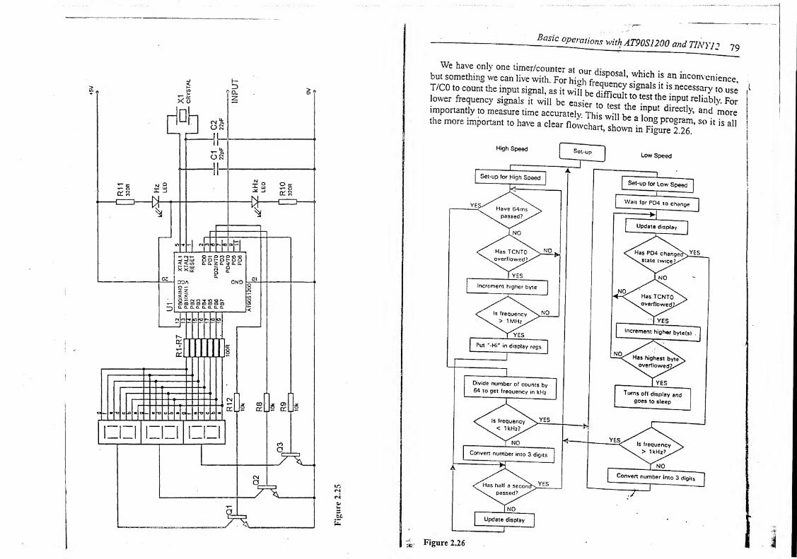
AS*
320R
— wigArmmo and TMyjj 79
We have only one timer/counter at our riicr,r,ooi u- u •
but something we can live with. For hi«-h frPnP ’ WhlC
? !
s an “convenience,
T/CO to count the input signal, as h w 5 i2Z7, fT"*?“ ne“s®y » use
lower frequency signals it will Forimportantly to measure time accurately This will tS
I,”P dl,ectly
' a,ld morethe more important to have a dear flowchart, shol in
" “ “ a"
High SpeedLow Speed
Set-up for High Speed
Have 64ms
^ passed? .
Is frequency
> 1kHz? >
Has half a seconV passed?
Convert number into 3 digits
Update display
Figure 2.26
80 Basic operations with AT90S1200 and TINY12 Basic operations with AT90S1200 and TINY12 8
1
The test for high frequency signals takes the shortest time (64 ms), so the
program will run this first. If the frequency measured is less than 1 kHz, the
program will jump to the low-speed testing. The idea behind the high-speed
testing is to time 64 ms by counting clock cycles (i.e. without T/CO), and count
signals on T/CO. The only problem is that for timing up to 1 MHz, we would
expect 64 000 cycles, i.e. well above 256. We therefore need to be monitoring
T/CO to see when it overflows, and increment a counter which would act as a
i
higher byte for T/CO. You can now see why I chose 64 ms. The maximumnumber which can be stored over two registers is OxFFFF = 65 536, so 64 000
is close to the maximum. Furthermore to convert the number of counts into a
frequency in kHz, we need only to divide the number of counts by 64. Dividing
a number by 2n is easy - we simply rotate the number to the right n times (you
may want to try this out on paper). This makes 64 ms an ideal choice.
For the low-speed test, we change T/CO to count internally. We wait for the
input to change and then start timing, waiting until the input changes a further
two times before stopping again (this times the length of one cycle). Again, if
we look at 1 Hz. with T/CO counting at 4 MHz, this represents 4 million cycles,
and we will need three registers to hold the entire number. If the time is greater
than these three registers can hold we know the time is less than 1 Hz. and so
send the AVR to sleep. The WDT will be set to wake up the AVR every 1024
; ms (i.e. about once a second), though note that in normal operation the WDTwill have to be cleared regularly.
For the Init section, set up the ports with no pull-up on the input signal pin.
;Also, set up the WDTCR to enable the WDT to reset every 1024 ms, and
: configure MCUCR to enable deep (power-down) sleep.
We now need to carefully construct the main loop in which the timing will be
carried out - this is the most important part of the program. We can guess that
the loop is going to take somewhere between 4 and 10 cycles, so for 64 ms =
256 000 clock cycles, we are going to have to count down between 64 000 and
25 600 times, we can therefore make a guess that two counting registers
Delayl and Delay2) can be used to count the time, but we will have to actually
!
write the loop before we can be sure. Before we enter the loop we will have to
! >et up the delay registers (we don’t know what we will have to move into them
.is this depends on the loop length), set up how T/CO is going to count, and reset
T/CO to 0. We will also use the move Obi 0000000 into Port B to turn on the kHzLED and reset the display You will notice there is also a line clearing a register
called upperbyte, we will see the significance of this register shortly.
ldi Delayl, ?? 5
ldi Delay2, ??*
ldi temp, ObOOOOOlll ; sets T/CO to count rising edge
out TCCR0, temp ; on TO (PD4)
ldi temp, OblOOOOOOO ; turns off all displays and turns on
out PortB, temp; kHz LED
clr upperbyte ; clears a counting register
clr temp; resets Timer 0
out TCNTO, temp\
The loop itself starts with the standard decrementing of the 2-byte numberspread over the delay registers, skipping out of the loop if the time has passed:
Highspeed:
subi Delayl, 1 ; decrements Delaylsbci Delay2, 0 ; decrements Delay2 if carry highbrcs DoneHi
; jumps out ofloop if time passed
We then need some way of testing to see ifT/CO has overflowed. There are twoways of doing this. The simplest is to test the timer overflow flag, which, unlikethe other flags we’ve met so far. is stored in the TIFR I/O register.
Unfortunately, we cannot test this flag directly with the sbic orsbis instructions,as it is number 0x38 which is greater than Ox IF. We would therefore have toread TIFR into a working register, then test the bit. More irritating is the factthat we need to reset it by writing a one to it. Again, we cannot'use the sbiinstruction, and instead have to do it through a working register. This overallprocess takes five instructions, but there is an alternative method which onlyuses four. The concept behind this method is to store the current value ofT/COand compare it with the value that was in T/CO the previous time in the loop.We would expect the current value to always be greater than the previous value,except when it overflows. By comparing the old and new values, and branchingif the new is less than the old, we therefore detect an overflow, and no resettingof flags is needed. In the code below, we use register temp to store the newvalue, and temp2 to store the old value:
mov temp2, tempin temp,TCNT0cp temp, temp2brsh Highspeed
; copies temp into temp2 (old value)
; reads new value into temp
; compares old and new; loops back if new is ‘same or higher’
If you count through the total Highspeed loop of seven instructions, you willsee it takes eight clock cycles if T/CO doesn’t overflow (remember abranching instruction takes two clock cycles). What.jVe need to do now is
construct a similar loop that will increment the higher byte, see if it’s too high,decrement our counting registers, skip out if they’ve reached zero, and loopback to Highspeed, all in the same number ofclock cycles. This final part iscrucial to ensure the timing is perfect. Fortunately we can do it all, with a
$£ clock cvcje to snsirc! Wp tA */*!/,j cu - - .
•
82 Basic operations with AT90S1200 and TINY12
number of counts we are allowing on the input is 63 999 in the 64 ms (i.e. 1
MHz is just too high, and so 64 000 is just too high - 64 000 translates as
OxFAOO, which is handy as we can simply test if the upper byte has reached
OxFA). If it has we know how to skip out of the loop:
inc upperbyte ;increments higher byte
cpi upperbyte, OxFA ;too high?
breq TooHigh ;skips out of loop if too high
subi Delay1,
1
; decrements counting registers
sbei Delay2, 0 >
bres DoneHi ;skips out of loop if done counting
nop ;wastes one cycle
rjmp Highspeed ; loops back
Now you may be thinking ‘hang on, there are nine cycles in the above segment,
not eight!’. You are right, of course, but think about the number of cycles in the
previous section if the program does not loop back to Highspeed. If the
program does not loop back, it does not branch, and so takes one less clock
cycle. We make up for this one less clock cycle in the loop above with one more
in this loop. Thus in the running of this whole section, the counting registers
will either decrement once every eight clock cycles or twice every 16 clock
cycles. You may want to write the whole loop down and work through it to
convince yourself of this. Now that we know the delay registers decrement
every eight clock cycles, we can work out what to initialize them to in order to
create a 64 ms delay.
• EXERCISE 2.37 What should Delay 1 and Delay2 be initialized to?
That’s the hardest part done! We now need to immediately store the current
value ofT/C0. The only problem is, what ifT/C0 has overflowed in between the
last test for overflowing and now? We need to use the same test as before.
EXERCISE 2.38 Write the six lines which make up the section called DoneHi.
which stores T/C0 into lowerbvte. and compare this value with temp (which
represents the old value ofT/CO). If lowerbyte is ‘same or higher’ it skips to a
section called Divide64, if it isn’t, it increments upperbvte, tests to see if it has
reached OxFA, and jumps to TooHigh if it has.
The next section needs to divide the 2-byte number split up over lowerbvte and
upperbyte by 64 = 26 . We do this by rotating the whole number six times; to
rotate the upper byte into the lower byte, we rotate the upper byte right with zeros
filling bit 7, and then rotate the lower byte right with the carry flag filling bit 7.
exercise 2.39 What two lines divide the 2-byte number by 2?
Basic operations with AWOSf200 and TINY12 83
The Divide64 loop does this six times. First we set up temp with the number 6.
then divide by 2 as we’ve done above. Then decrement temp, looping back if it
does not equal zero. We don’t want to reset temp with 6, so we really want to
jump to Divide64 and then skip one instruction. This can be done using the
following trick:
rjmp Divide64+1;jumps to Divide64 and then skips one
This works with any jumping/branching instruction, and for any number ofskips. Note that large skips (e.g. +8) lead to unwieldy programs which are hardto follow and easy to get wrong.
exercise 2.40 What five lines make up the Divide64 section?
We test to see if the number is too low. The 2-byte word holds the frequency in
kHz, so if this number is less than 1 (i.e. 0) we know how to change to the low-speed testing method.
exercise 2.41 What four lines test to see if both bytes are 0, and skips to
LowSpeed if they are.
Wc then need to convert this number split over 2 bytes into a number ofhundreds, tens and ones so that they can be displayed easily. This will be donein a subroutine, as we will have to do it in the LowSpeed section as well. To dothe conversion we will call DigitConvert. As the displays are being strobed, weneed to be calling a display subroutine at regular intervals. Unfortunately, ourcarefully constructed timing loop above. cannot accommodate the calling of a
display subroutine, as this would insert large numbers of clock cycles anddisrupt the timing. The timing routine only takes 64 ms, so the idea here is to
leave the displays idle for 64 ms, and then let them run for half a second.We stick in a simple half second delay using counting registers, making sure
we call the Display subroutine during the loop.
exercise 2.42 Write the nine instructions which set up the three delay regis-
ters, and then create a half second delay loop which also calls Display. Whenthe required time has passed, the program should jump back to Start. You will
have to take the length of the Display subroutine into account when doing yourcalculations. The rcall instruction actually takes three cycles, and the ret
instruction takes four. On average, the subroutine itself, will take two instruc-
tions, so assume the whole subroutine action adds ninejefock cycles to the loop.‘ Call the delay loop HalfSecond.
> All that remains in the high-speed timing method is to deal with the TooHigh
|section, which simply has to make the display registers show -HI. The numbers
84 Basic operations with AT90S1200 and TINY12
to be displayed will be stored in registers called Hundreds, Tens and Ones.
There will be a look-up table as before, except in this table 1 0 will be translated
as the symbol for an *H\ and 11 as the symbol for a hyphen A 12 will be
translated as a blank space (i.e. no segments on), and so you should set all digits
to 12 in the Init section. We therefore need to move 11 into Hundreds, 10 into
Tens and a 1 into Ones (as a 1 will look like an I), and the Display subroutine
will do the rest. After this we jump to three lines before the start HalfSecond
section (these three lines previously set up the HalfSecond counting registers).
EXERCISE 2.43 What/ow lines make up the TooHigh section?
This marks the end of the high-speed timing method, and therefore the halfway
point in the program.
Let’s have a lopk at the DigitConvert subroutine. This takes a number split
over upperbyte and lowerbyte, and converts it into a number of hundreds, tens
and ones. This is done by repeatedly subtracting 100 from the 2-byte number
until there is a carry. 100 is then added back, and the process is repeated with
1 0. The number left in the lower byte after this is simply the number of ones, so
we can just move the number across. Once we have extracted the number of
hundreds, wc no longer need to involve the upper byte, as we know the number
is now entirely contained in the lower byte (if the number is less than 100 it fits
in one byte).
DigitConvert:
cir Hundreds
clr Onescir Tens
resets registers
FindHundreds:
subi
sbci
brcs
inc
rjmp
FindTens:
subi
subi
brcs
inc
rjmp
FindOnes:
subi
lowerbyte, 100 ;subtracts 100 from lower byte
upperbyte, 0 ;subtracts 1 if carry
FindTens;does 10’s if carry
Hundreds : increment number of hundreds
FindHundreds;repeats
lowerbyte, -100;adds back the last 100
lowerbyte, 10 ;subtracts 10 from lower byte
FindOnes ;does l’s if carry
Tens ;increments number of tens
FindTens+1 ;repeats, but doesn’t add 100 again
lowerbyte, -10 ; adds back the last 10
Basic operations with AT90S1200 and TINY12 85
mov ones, lowerbyte; number left in lowerbyte = ones
ret; finished
You may .want to work your way through this program with a sample number(e.g. eonvinee yourself that 329 gets reduced to 3 hundreds, 2 tens and 9 ones).The other subroutine is Display. This has to choose which of the three
displays to activate, find the appropriate number in Hundreds, Tens or Ones,and then display it. In the half second loop we’ve written, the subroutine iscahed about once every 4 ms. We can’t make the displays change this often asthe LEDs won t have time to turn fully on and the display will -be faint withshadows (numbers on other displays appearing on the wrona display). We there-fore build m an automatic scaling of 50 - i.e. the subroutine returns immedi-ately having done nothing 49 times, and then on the 50th time its called, itperforms the display routine, and then repeats. This means the displays arec anging every 0.2 ms which is far better: however, should you experience anvof the efiects described above, you may wish to increase 50 to a hicher value
*
We win use a register called DisplayCounter. This will be set up in the lnitsection with the value oO. The beginning of Display therefore decrementsDisp ayCounter. and returns if the result is not 0. If it is 0. DispiavCountershould be reloaded with M). Furthermore, wc can take this opportunity to clearwatchdog timer. This must be done regularly, and the Display subroutine iscalled regularly in whichever part of the program it happens to be (by regularlymean at least once a second). A simple solution is therefore to reset the WDTwhen the Display subroutine continues.
exercise 2.44 Write the five lines at the start of the Display subroutine.
We need some way to know which display we will be displaying and will storethis as a number between 0 and 2 in a register called Display,Number.Therefore, the first thing we do is increment DisplavNumber and reset it to 0
i as reac e j (you will also have to clear DisplavNumber in the Initsection).
perfomE
thiS
45 Wrhe thC subsequent four Iines of the subroutine which
Now we need to do some serious indirect addressing! First, we extract the rmhtnumber to be displayed from Hundreds, Tens or Ones. You will have to define
w program’ 1 defined mine as R2£ R27 and R28 respec-
tsy‘ ther
^ore set UP ZL t0 point to R26 (move 26 into ZL). and then add
wantTrf!" D 'Sp,ay*TJber - This wi“ P°int t0 one of the three numbers we
jrod>spl
f Us,n§ the ,d instruction we load this value into temp. The sevense^nent display codes are stored in registers R0-R12, and so we now zero ZLRO (move 0 into it). Addins to R0 the
86 Basic operations with AT90S1200 and TINYJ2 Basic operations with AT90S1200 and TINY12 87
the seven segment code of the number to be displayed. Again, load this value
into temp. We mustn’t clear bit 7 of PortB if it is on (indicating kHz). Therefore,
test bit 7 of Port B, if it is on, OR the number in temp with Ob 10000000, and
then in either case move temp into Port B.
in
eor
sbrs
rjmp
store2, PinDstore2, store
store2,
4
FirstChange
; reads in current value
; EORs current and initial values
; skips out of loop if PD4 changed
; keeps looping until PD4 changes
exercise 2.46 Write the nine lines which output the correct seven segment
code to Port B.
The remainder of the subroutine must turn on the correct seven segment display.
Remember the essence of strobing: the number you have just outputted to Port
B is going to all of the displays, but by turning only one ofthem on, the number
only appears in one of the displays. We basically want to turn on PortD bit 0.
then bit 1, then bit 2 and then back to bit 0. The easiest way to do this is to read
PinD into temp, rotate it left without letting any Is creep in (i.e. use Isl), test to
see if bit 3 is high (i.e. gone too far), and reset the value to ObOOOOOOOl if it is.
exercise 2.47 What six lines turn on the correct display and then return from
the subroutine?
Now all that is left is the low-speed testing section. We need to set up T/C0 to
count up every clock cycle (this gives us maximum resolution). We also need to
(reset) clear the delay registers Delay2 and Delav3. and clear PB7 to turn on the
Hz LED.
EXERCISE 2.4S Whatfive lines will start off the LowSpeed section?
We need a way to see when PD4 changes (remember now T/C0 is counting
internally we need to test the input pin manually). There are a few methods at
our disposal, the one 1 suggest is as follows. Store the initial value in PinD. and
then enter a loop which reads in the current value of PinD. and exclusive OR it
with the initial value. The effect of the EOR is to highlight which bits are
different.
Example 2.
9
ObOOO 11001
EOR Obi 0001001
OblOOlOOOO «- shows that bits 7 and 4 were different
We are interested only in bit 4 (PD4) which is connected to the input, and so
after performing the EOR we can test bit 4 of the answer and keep looping until
it is high. When in any loop that lasts a long time (as this one might), we must
also keep calling the Display routine.
in store, PinD ;stores initial value
The main loop of the low-speed testing section consists of repeating the abovetest for two changes (i.e. wait for one complete period ofthe input’s oscillation),
and incrementing the higher bytes when T/C0 overflows. We deal with the T/C0overflow in the same way as before, with one important difference. We cannotuse temp to store the old value because temp is used repeatedly in the Displaysubroutine we have just written. It is very important you look out for these kindsof traps as they can be a source of many problems - try to keep your use ofworking registers local (i.e. don’t expect them to hold a number for too long),in this way you can use a register like temp all over the program. We can useDelayl instead of temp, as at the end of the looping, we want Delayl to holdthe current value in T/C0.
Before we enter the low-speed loop we need to clear Delayl and T/C0. Wewill also need some sort- of counter to count the number of times the inputchanges. We need it to change only twice, so. set up a register called Counterand load 2 into it.
!
exercise 2.49 Write the three pre-loop instructions.
Now the loop looks for a change in the input in the same way as before, andjumps to a section called Change if there is a change.
t
exercise 2.50 Write they/ve lines which perform this test. (HINT: One ofthem is before the start of the loop, call the loop LowLoop.)
We then call the Display subroutine, as we have to do this regularly, then test tosee if the T/CO has overflowed. If it hasn’t overflowed, loop back to LowLoop.If it has overflowed, increment Delay2, and if this overflows increment Delay3.The minimum frequency is 1 Hz. and hence the maximum amount of time is
about 4 000 000 counts, which in hexadecimal is Ox3D0900. Therefore if
Delay3 reaches 0x3E we know the input frequency is too slow and will jump toa section called TooSlow.
EXERCISE 2.51 Challenge.' What 11 lines form the rest of the low-speedsection. j
The Change section should decrement Counter, and loop back to LowLoop if
it isn’t zero. On the second change, it doesn’t loop back but instead checks tosee if the stored number is low enough to deserve high-speed testing. The
88 Basic operations with AT90S1200 and TINY12
to 4004 clock cycles, hence if the result is 4000 (OxFAO) or less we should
branch to Start and perform the high-speed testing. It may not be entirely clear
how we test to see if the number spread over three registers is less than
OxOOOFAO. For a start, we cannot subtract the number, as this would change the
number in the delay registers. Instead, we use the compare instructions as wewould ifwe were just testing one byte, but also make use of the cpc instruction,
which compares two registers and also takes the carry flag into account. It is
simply analogous to subtracting with the carry (e.g. sbci but without actually
changing the registers). The only problem with cpc is that it only works between
two file registers, not a file register and a number, so we have to load the
numbers into temporary' working registers. The necessary lines for Change are
Itherefore:
Change: in store, PortB ; updates new value of PortB
dec Counter : waits for second change
brne LowLoop ; not second change so loops
ldi temp, OxOF ; sets ups temporary registers
Idi temp2, 0x00 ;
cpi Delay 1, OxAO : compares three-byte number with
cpc Delay2, temp ; OxOOOFAOcpc Delay3, temp2 ;
brcc PC+2 ; less that FA0 so goes to high-speed
rjmp Start ;
You will notice that instead of the expected line (brcs Start) - i.e. branch
to Start if the carry flag is set, we choose to skip the (rjmp Start) line if
the carry flag is clear. These two methods are clearly identical in their end
result, but why introduce an extra line? The reason lies in the fact that the brcs
can only branch to lines which are 64 instructions away. The Start line is, in
fact, further away than this, and so must be branched to using the rjmp instruc-
tion. Points like this will be picked up when you try to assemble the program
and are generally missed at the writing stage - so you don’t have to start
counting 60 odd lines whenever you introduce a brcs or similar instruction.
We then convert the time period of the oscillation into a frequency. To do this
we need to take 4 000 000 and divide it by the length of time (in clock cycles)
we have just measured. If we measured 40 000 clock cycles over one period
rhis will correspond to 1 00 Hz. There is a way to perform binary long division,
out by far the simplest method of dividing x by y is to see how many times you
jan subtract y from x. This does take fewer instructions, but will take longer to
nin. We set up 4 000 000 = 0x3D0900, spread over three temporary registers
t temp, temp2 and temp3). Every time we successfully subtract the number
spread over Dclayl, Delay2 and Delay3, we increment a lower byte of the
i answer. When this overflows, we increment the higher byte. The answer will be
Basic operations with AT90S1200 and TINY12 89
between 1 and 1000 so we need only two bytes for the answer. The followinglines set up the division:
ldi temp, 0x00; moves 4 000 000 spread over 3
ldi temp2, 0x09; temporary registers
ldi temp3, 0x3D;
clr lowerbyte; resets the answer registers
clr upperbyte;
exercise 2.52 Write the eight lines of the loop called Divide which divides4 000 000 by the number in the delay registers. (Hint: Call the next sectionDoneDividing and jump to this section when a subtraction was unsuccessful(carry flag was set).)
As with the high-speed section, we then convert the number in lowerbyte andupperbyte into hundreds, tens and ones. We can use the DigitConvert subrou-tine we have already written. The program then loops back to LowSpeed.
exercise 2.5j What iwo lines wrap up the low-speed testing loop?
All that remains is the section called TooSlow which is branched to when theperiod of oscillations is more than one second. In this case wc want to turn thedisplays off and send the AVR to sleep.
EXERCISE 2.54 Write the three lines which make up the TooSlow section.
You will have to remember to set up registers R0 to R1 1 with the correct sevensegment code in the Init section. As you can use only the ldi instruction onregisters R16-R31 you will have to move the numbers first into temp, and thenmove them into R0 to R1 1 using the mov instruction. Also, remember to set upRortD with one of the displays selected (e.g. ObOOOOOOOl), and define all yourregisters at the top of the program. It should now be ready for testing with thesimulator. This may be worth building as it performs a usefurfunction:however, you will notice that its resolution isn’t great as vou aet onlv three-figure resolution between 100 Hz-999 Hz and 100 kHz-999 kHz. You maywant to think about ways to improve the^program to give three-figure resolu-tion for all frequencies in the given range. In the coming chapters we will learnmethods that will allow us to simplify this program hugely, and it will be worthcoming back to this at the end and gleefully hack bitsiffto trim down theprogram.
Working on this larger program also introduces the importance of taking
|r®aks - Even wlien y°u arc ‘m the zone’ it is always a good idea to step back forfew minutes and relax. You will find you return looking at the bigger picture
90 Basic operations with AT90S1200 and TINY12
help reduce such oversights. Another good piece of advice is to talk to peopleabout decisions you have to make, or problems when you get stuck. Even if thevdon’t know the first thing about microcontrollers, simply asking the questionwill surprisingly often reveal the answer.
Sntroducing the rest
of the family
So far, we have been looking at the most basic types of AVR, the 1200 and the
Tiny AVRs. I will now introduce some of the differences between these and
other AVRs, so that in the subsequent chapters they might appear more familiar.
Other models may benefit from extra memory called RAM. The allocation of
memory differs in different models, but follows the arrangement shown in
Figure 3.1.
i
Figure 3.1
The first 32 addresses are the working registers afid the next 64 are the I/O
registers. So the key difference between those with RAM and those without is
the presence of further memory spaces from $60 onwards. These can be t
accessed using the Id and st commands already introduced, and with otherj
instructions now available on these more advanced models. A significant[
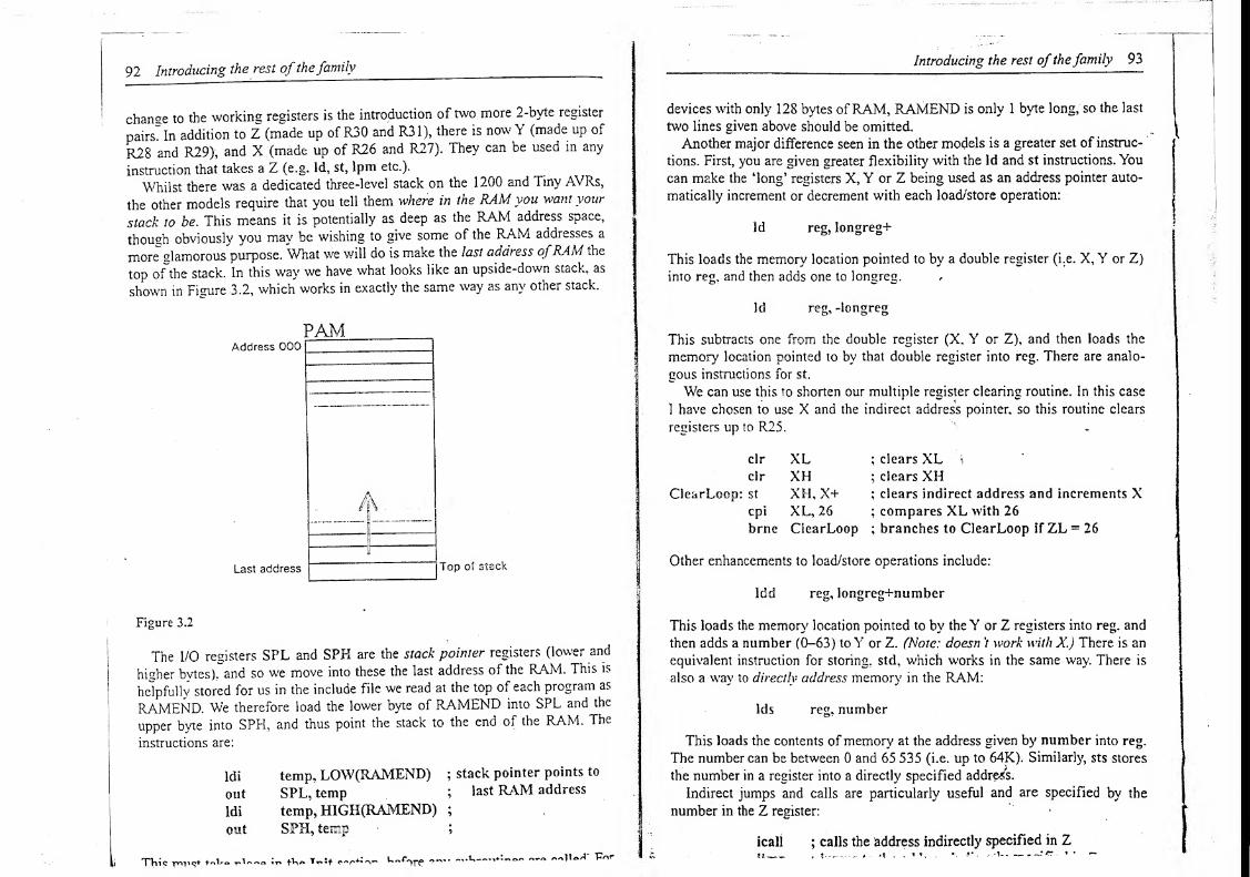
92 Introducing the rest ofthefamily
chanae to the working registers is the introduction of two more 2-byte register
pairs' In addition to Z (made up of R30 and R3 1), there is now Y (made up of
R28 and R29), and X (made up of R26 and R27). They can be used m any
instruction that takes a Z (e.g. Id, st, 1pm etc.).
Whilst there was a dedicated three-level stack on the 1200 and Tiny AVRs,
the other models require that you tell them where in the RAM you want your
stack to be. This means it is potentially as deep as the RAM address space,
though obviously you may be wishing to give some of the RAM addresses a
more glamorouspurpose. What we will do is make the last address ofRAM the
top of the stack. In this way we have what looks like an upside-down stack, as
shown in Figure 3.2, which works in exactly the same way as any other stack.
PAMAddress OOO
Last address Top of stack
Figure 3.2
The I/O registers SPL and SPH are the stack pointer registers (lower and
higher bytes).'and so we move into these the last address of the FLAM. This is
helpfully stored for us in the include file we read at the top of each program as
RAMEND. We therefore load the lower byte of RAMEND into SPL and the
upper byte into SPH, and thus point the stack to the end of the RAM. The
instructions are:
ldi temp, LOW(RAMEND) ; stack pointer points to
out SPL, temp ;last RAM address
ldi temp, HIGH(RAMEND) ;
out SPH, temp ;
TVli<? foVo
Introducing the rest ofthefamily 93
devices with only 128 bytes ofRAM, RAMEND is only 1 byte long, so the last
two lines given above should be omitted.
Another major difference seen in the other models is a greater set of instruc-
tions. First, you are given greater flexibility with the Id and st instructions. You
can make the ‘long’ registers X, Y or Z being used as an address pointer auto-
matically increment or decrement with each load/store operation:
Id reg, longreg*
This loads the memory location pointed to by a double register (i.e. X, Y or Z)
into reg. and then adds one to longreg.
Id reg, -longreg
This subtracts one from the double register (X. Y or Z), and then loads the
memory location pointed to by that double register into reg. There are analo-
gous instructions for st.
We can use this to shorten our multiple register clearing routine. In this case
1 have chosen to use X and the indirect address pointer, so this routine clears
registers up to R25. 1
clr
clr
ClearLoop: st
cpi
XL ; clears XL 'i
XH ; clears XHXH, X+ ; clears indirect address and increments XXL, 26 ;
compares XL with 26
brne ClearLoop ; branches to ClearLoop if ZL » 26
Other enhancements to load/store operations include:
Idd reg, longreg+number
This loads the memory location pointed to by theY or Z registers into reg, and
then adds a number (0-63) to Y or Z. (Note: doesn V work with X) There is an
equivalent instruction for storing, std, which works in the same way. There is
also a way to directly address memory in the RAM:
Ids reg, number
This loads the contents ofmemory at the address given by number into reg.
The number can be between 0 and 65 535 (i.e. up to 64K). Similarly, sts stores
the number in a register into a directly specified address.
Indirect jumps and calls are particularly useful and are specified by the
number in the Z register:
icali;calls the address indirectly specified in Z
94 Introducing the rest ofthefamily
Example 3.1 We have a program that has to perform one of five different
functions, depending on the number in a register called Function. By adding
Function to the current value of the program counter, and jumping to that
address, we can make the program branch out to different sections:
clr ZH ;makes sure higher byte is dear
ldi ZL, JumpTabie;points Z to top of table
add ZL, Function;adds Function to Z
ijmp ;indirectly jumps
JumpTabie: rjmp Addition;jumps to Addition section
rjmp Subtraction;jumps to Subtraction section
rjmp Multiplication;jumps to Multiplication section
rjmp Division;jumps to Division section
rjmp Power;jumps to Power section
Notice that JumpTabie is loaded into Z, this is translated by the assembler as
the program memory address of the line it is labelling. We do this to initialize
Z to point to the top of the branching table (rjmp Addition). Note that
loading JumpTabie is equivalent to loading PC+3. The number in Function is
then added to Z, so that the number in Function (between 0 and 4) will make
the program jump to one of the five sections.
You will no doubt remember the number of additions and subtractions we had
to do to 2-byte numbers in the frequency counter project. Here are two newinstructions that may help:
adiw longreg, numbersbiw longreg, number
These add or subtract a number between 0 and 63 to/ffom one of the 16-bit
registers (X, Y or Z). The ‘w!
stands for word (16 bits). If there is an overflow
or carry this is automatically transferred onto the higher byte. Hence:
subi XL, 50
sbci XH, 0sbiw XL, 50
The two remaining instructions that are added to the repertoire of the moreadvanced AVRs are:
push register
pop register
So far we have only been using the stack for the automatic storage of programcounter addresses when calling subroutines. Using these instructions, you can
push or pop the number in any working register on to or off of the stack.
Introducing the rest ofthefamily 95
Example 3.2 We can use the push and pop instructions to create a palindrome
detector. A palindrome is essentially a symmetric sequence (like ‘radar’,
‘dennis sinned’ and ‘evil olive’). We can massively simplify this problem by
also requiring that we are given the length of the input sequence. We can use the
length to find the middle of the input. We can also assume that the input is fed
(as an ASCII character) into a register called Input. ASCII is a way to translate
letters and symbols into a byte, so each letter corresponds to a particular byte-
long number. So effectively we are looking for the sequence of bytes fed into
Input to be palindromic (symmetric). We start by pushing the number in Input
on to the stack. We do this for every new input until we reach the half-way point.
We then sxznpopping the stack and comparing it with the input. As long as each
new input continues to be the same as the popped number, the sequence is
potentially palindromic. If the new input fails to be the same as the popped
number, we reject the input sequence. PinD, bit 0 will pulse high for
1 microsecond to indicate a new input symbol (we need this because we cannot
just wait for the input symbol to change, as this would not respond to repeated
letters).
First, we assume the length of the word is stored in Length. This has to be
divided by two to get the half-way point. We will have to make a note if the
length is odd or not. This is done by testing the carry flag: if it is high Length
was odd and we shall set the T bit.
Start: mov HalfLength, Length divides Length by 2 to get
lsr HalfLength HalfLength
in temp, SREG ; copies Carry flag into T bit
bst temp, 0 ;i.e. sets T-bit if Length is odd
Assuming the first input byte is in Input, we push it on to the stack and then
wait for the pulse on PinD, bit 0. The pulse lasts 1 microsecond, so assuming a
4 MHz clock it must be tested at least once every four cycles. In the segment
below, it is tested once every three cycles.
FirstHalf: push Input;pushes Input onto stack
Pulse: sbis PinD, 0 ; tests for pulse
rjmp Pulse ; keeps looping
When a pulse is received (i.e. a new input symbol is ready), the program incre-
ments Counter which is keeping track of the input number. It compares this
number with HalfLength and loops back as long as Counter is less than
HalfLength. J
inc Counter ;counts the input number
cp Counter, HalfLength ;compares with half-way value
brio FirstHalf ;loops back to start and skips one
96 Introducing the rest ofthefamily
When Counter equals HalfLength we check the T bit to see if the length of the
input is odd or even. If it is odd, we need to ignore the middle letter, so we reset
the T bit and loop back to Pulse which will wait until the next input is ready. If
the length is even we can skip on to test the second half of the input.
brtc SecondHalf ; test T bit
clt ;clears T bit
rjmp Pulse ;
We have now passed the half-way point in the sequence and now the new input
svmbols must match the previous ones. The top of stack is popped and
compared with the current input. If they are not equal the sequence is rejected.
SecondHalf: pop Input2 ; pops stack into Input2
cp Input, Input2 ; compares Input and Input2
brne Reject ; if different reject sequence
As before, we then increment Counter and test to see if Couiiter equals
Length. If it does, the testing is over and we can accept the input. If we haven't
vet reached the end the program then waits for the input to change, and then
loops back to SecondHalf.
inc Counter ; counts the input numbercp Counter, Length ; compares with total length
breq Accept ; end of sequence so accept
. Pulse2: sbis PinD, 0 ; waits for pulse
rjmp Pulse2 ;
rjmp SecondHalf ; loops back when new input is
. ; ready
You might want to play around with this on the simulator, but don’t forget to set
up the top of the stack as described at the start of the chapter. You may also want
to think about how to remove the need to be given the length of the input
sequence. Ifyou want to find out more about this, you may want to find a book
on Formal Languages and Parsing.
4Intermediate operations
|
Interrupts
So far we have always had to test for certain events ourselves (e.g. test for a
button to be pressed test if T/CO has overflowed etc.). Fortunately there are a
number of events which can automatically alert us when they occur. They will,
if correctly set up, interrupt the normal running of the program and jump to a
specific part of the program. These events are called interrupts.
On the 1200. the following interrupts are available:
• Interrupt when the INTO pin (PD2) is low
• Interrupt when there is a rising edge on INTO
• Interrupt when there is a falling edge on INTO
• Interrupt when T/CO overflows
• Interrupt when the Analogue Comparator triggers a result
The first three constitute an external interrupt on INTO, and are mutually exclu-
sive (i.e. you can enable only one of the three interrupts at any one time). The
significance of the Analogue Comparator will be discussed later on in the
chapter. When an interrupt occurs, the program will jump to one of the addresses
at the start of the program. These addresses are given by what is known as the
interrupt vector table . The interrupt vector table for the 1200 is shown in Table
4.1, the tables for the other AYR types are shown in Appendix E.
Type of Interrupt/Reset Program jumps to address ...
Power-on/Reset
External interrupt on INTO
T/CO overflow interrupt
Analogue comparator interrupt
For example, when the T/CO overflow interrupt is ’enabled, and T/CO over-
flows, the program drops what it’s doing and jumps to, address 0x002 in the
program memory. When using all three interrupts, the start *of the program
should look something like the following:
98 Intermediate operations
rjmp Init
rjmp Extint
rjmp Overflowlnt
rjmp ACInt
;first line executed
; handles external interrupt
;handles TCNTO interrupt
;handles A. C. interrupt
This will ensure the program branches to the correct section when a particular
interrupt occurs (we will call these interrupt handling routines). We can enable
individual interrupts using various registers. The enable bit for the External
INTO interrupt is bit 6 in an I/O register called GIMSK (General Interrupt
Mask). Setting this bit enables the interrupt, clearing it disables it. The enable
bit for the TCNTO overflow bit is bit 1 in the TIMSK I/O register (Timer
Interrupt Mask). However, all of these interrupts are overridden by an inter-
rupts ‘master enable'. This is a master switch which will disable all interrupts
when off, and when on it enables all individually enabled interrupts. This bit is
the I bit in SREG (you may want to glance back to page 73).
The External INTO interrupt can be set to trigger in one of three different
circumstances, depending on the states of bits 0 and 1 ofthe MCUCR I/O register
(the one that also holds the sleep settings). This relation is shown in Tabic 4.2.
Table 4.2
MCUCRBitl Bit 0
Interrupt occurs when
INTO is low
Invalid selection
There is a falling edge on INTO
There is a rising edge on INTO
When an interrupt occurs, the value of the program counter is stored in the
stack as with subroutines, so that the program can return to where it was when
the interrupt handling is over. Furthermore, when the interrupt occurs, the
master interrupt enable bit is automatically cleared. This is so that you don’t
have interrupts occurring inside the interrupt handling routine which would
then lead to a mess of recursion. You will probably want to re-enable the master
interrupt bit upon returning from the interrupt handling routine. Fortunately
there is a purpose-built instruction:
This returns from a subroutine and at the same time enables the master inter-
rupt bit.
Each interrupt also has an interrupt flag. This is a flag (bit) that goes high
when an interrupt should occur, even if the global interrupts have been disabled
Intermediate operations 99
and the appropriate interrupt sendee routine isn’t called. If the global interrupts
are disabled (for example, we are already in a different interrupt service routine), j
you can test the flag to see if any interrupts have occurred. Note that these flagsj
stay high until reset, and an interrupt service routine will be called if the flag is T
high and the global interrupt bit is enabled. So you must reset all flags before
enabling the global interrupt bit, just in case you have some interrupt flags
lingering high from an event that occurred previously. Interrupt flags are reset
by setting the appropriate bit - this sounds counterintuitive but it’s just the waythings are! The T/CO Overflow interrupt flag is found in bit 1 of TIFR (Timer
Interrupt Flag Register - I/O number S38), and the INTO interrupt flag is in bit
6 of GIFR (General Interrupt Flag Register - I/O number S3A).
Program K: reaction tester
• Interrupts
• Random number generation
• Seven segment displays
The next example program will be a reaction tester. A ready button is pressed,
then an LED will turn on a random time later (roughly between 4 and 12
seconds). The user has to press a button when they see the LED turn on. Theprogram will measure the reaction time of the user and display it in millisec-
onds on three seven segment displays. If the user presses the button before the
LED turns on they will be caught cheating. The circuit diagram for the project
is shown in Figure 4.1, and the flowchart in Figure 4.2.
We will be using the External INTO and TCNTO Overflow interrupts, so youwill have to make the necessary changes to the top of the program. Note that as
we will not be using the Analogue Comparator interrupt we don’t need anyparticular instruction at address 0x003.
EXERCISE 4.1 What are the first three instructions of the program?
Write the Init section, setting T/CO to count internally at CK/1024. You will
have to enable the External INTO and T/CO Overflow interrupts, but don’t set
the master enable just yet. Set the External INTO interrupt to occur when INTOis low (i.e. when the button is pressed). 1
exercise 4.2 What are the six lines which individually enable the interrupts?
./At Start we first call the Display subroutine, and then test the ‘Ready’ button
(PinD, 1). Keep looping until the Ready button is pressed.
exercise 4.3 What three lines achieve this?
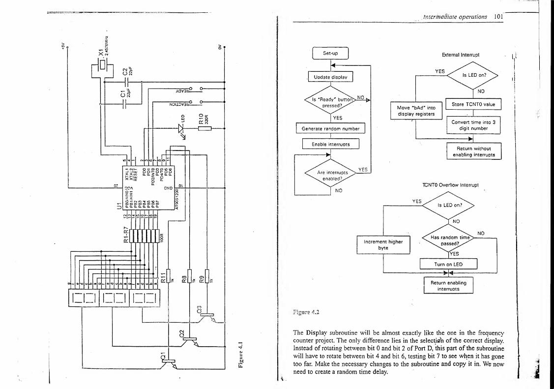
Figure
4.1
The Display subroutine will be almost exactly like the one in the frequency
counter project. The only difference lies in the selection of the correct display.
Instead of rotating between bit 0 and bit 2 of Port D, this part of the subroutine
will have to rotate between bit 4 and bit 6, testing bit 7 to see when it has gone
too far. Make the necessary changes to the subroutine and copy it in. We nowneed to create a random time delay.
1 02 Intermediate operations
Random digression
One of the interesting aspects of this program will be the generation of the
random number to produce a time delay of random length. The most straight-
forward method for generating random numbers is to rely on some human input
and convert this into a number. For example, we could look at the number in
T/CO when the ‘Ready’ button is pressed. T/CO, if counting internally, will be
counting up and overflowing continuously, and so its value when the button is
pressed is likely to be random. Very often, however, we don’t have the luxury of
a human input, and so we have to generate a string of random numbers. How is
this done? There are a large number of algorithms available for generating
random numbers, varying in complexity. We are restricted in the complexity of
the functions we can straightforwardly apply usingAVR assembly language, but
fortunately one of the more simple algorithms relies purely on addition and
multiplication. The Linear Congruential Method developed by Lehmer in 1 948 1
has the following form:
! L,= mod (al + c)
This generates the next number in the sequence by multiplying the previous
number by a . adding c. and taking the result modulo m. modm(.v) is equal to the
remainder left when you divide .v by m. Conveniently, the result of every oper-
ation performed in an AVR program is effectively given in modulo 256. For
example, we add 20 to 250. The ‘reaF answer is 270: however, the result given
is 14 . 14 is4
270 modulo 256’ or mod->56(270). There are a number of restric-
tions on the choice of a and c in the above equation that maximize the random-
.ness of the sequence (see the reference for more info). Given that the quickest
algorithm is that with the smallest multiplier (a)y we will choose a ~ 5 and c - !.
You also have to pick a ‘seed’ - the first number in the sequence (70). You can
set this model up on a spreadsheet and examine its quasirandom properties.
First, you should notice that the randomness of the sequence does not appear
sensitive to the seed; there is therefore no need to pick a particular one. You will
also notice the sequence repeats itself every 256 numbers - this is an unfortu-
nate property of the algorithm. Picking a larger modulus will increase the repe-
tition period accordingly. We could use modulo 65 536 by using one of the
2-byte registers (X, Y or Z) and the adiw instruction. This would result in a
sequence that repeats only every 65 536 numbers! For our purposes with the
reaction tester, a period of 256 is quite acceptable.
To convert this random number into a random time we do the following. The
maximum time is 10 seconds, and the T/CO will overflow every 256 counts =
256/2400 = 0.066 second. We therefore would like a counter with a value
roughly 61 and 183. You might notice the difference between these numbers is
See reference on random numbers in Appendix 1.
Intermediate operations 103
1 51?/‘S m f
?V22)' °Ur hfe is made a !ot easier if the difference is128, so as the times needed are quoted only as approximate figures, we can use“Un er tha* 8°“ from 60 to 1 88 which will perform adequately. To convert ourom number between 0 and 255 we first divide by two, then add 60.
nnmSTw8
1
° program’ we wil1 use register Random to hold the randomnumber We need then to multiply this by five (add it to itself four times), and
then add one to it.
EXERCISE 4.4 What six lines will generate the next random number?
EXERCISE 4.5 What three lines will copy 'Random into CountX. divideCountX by two. and then add 60.
We then need to reset the higher byte of the timer (TimeH), turn off the displays
enable
P° B ’^ 3 ** ,ntem,pt flags’ and then set the master interrupt
EXERCISE 4.6 Which six lines will reset TimeH. PortB and the interrupt flags?
There is a particular instruction for setting the master interrupt enable:
se; Sets the interrupt enable bit.
The rest of the program is a loop which just tests the interrupt enable bit. andoops back to Start when it has been cleared. This is because after an ExternalINTO interrupt, the master interrupt bit will not re-enable interrupts and upon’returning the program will loop back to Start. In contrast, after a T/CO relatedinterrupt the interrupts will be re-enabled so the program will stay in the loop.
exercise 4.7 What three lines finish off the main body of the program?
Looking first at the T/CO overflow interrupt handling routine (Tint), we see thatthe first test is to see whether or not the LED (PinD. 0) is on. If it is off weshould be timing out the random time to see when to turn it on. If it is alreadyon we shoidd be incrementing the higher byte of our timing registers (TimeH).
_ ®^ exceeds the maximum that can be displayed on the scope, we should
xu Si'"10 he dlSplay reglsters return without enabling interrupts,
v k lC° 'S co“ntmg UP 2400 times a second (with a register countin® the
higher byte as well). We need to convert this to milliseconds (i.e. somethingcounting 1000 times a second). To do this we can multiply the 2-byte numbery and then divide by 12. Applying the reverse procedure to 999 (themaximum response time) we get 2397 = 95D. It would be much easier if we
were testing only to see ifthe higher byte had reached a certain value (e.g. A00)|
This is easy to do by resetting T/CO to 0xA2 when the LED is turned nn Ja
Intermediate operations
then subtract the 0xA2 back off the final answer at the end of the day:
Tint LEDon:
sbic PinD, 0 ;tests LED
rjmp TInt_LEDon ;jumps to different section if on
dec CountX ;decrements random counter
breq
reti
PC+2 ;skips if clear
;returns otherwise
sbi PortD, 0 ;turns on LED when time passes
ldi temp, 0xA2 ;initializes TCNTO to 0xA2
out
reti
TCNTO, temp ;to facilitate testing for max
>
n:
inc TimeH ;increments higher byte
cpi TimeH, OxOA ;tests for maximum time
breq
reti
PC+2 ;skips if the user is too slow
ldi Hundreds, 13
ldi Tens, 14 ; h
ldi
ret
Ones. 1 ; i
;returns without setting I-bit
The External INTO interrupt handling routine is more straightforward - we will
call it Extint. This also involves testing the LED first. If it isn’t on this means
the user has cheated bv pressing the button before the LED has turned on. In
this case, we move numbers 10, 11 and 12 into Hundreds, Tens and Ones
respectively in order to display ‘bAd’, and then return without re-enabling the
master interrupt bit. If the LED is on, the press is valid, and so we have to halt
the T/CO and store the current time by moving T/CO into TimeL. It is possible,
however unlikely, that the T/CO overflowed just after the INTO interrupt
occurred. We therefore need to test the T/CO overflow interrupt flag, and incre-
ment TimeH if it is set. Then the total reaction time (split up over TimeL and
TimeH) needs to have 0xA2 subtracted from it (as this was artificially added).
It must then be multiplied by 5 and divided by 1^..
exercise 4.8 Which 12 lines test the LED at the start of Extint, test the LED,
jump to a section called Cheat if it isn’t on, and halt the T/CO and store the
current value, incrementing TimeH if necessary? 0xA2 should then be
subtracted from the total reaction time, and T/CO should be restarted at
CK/1024.
fxfrOSf 4 c> Which- four lines form the Cheat section?
Intermediate operations 105
After subtracting 0xA2 we need to multiply the time by 5. As the time is split
over two registers we need to use the adc to add a carry to the higher byte if and.
when there is a carry:
idi Count4,
4
mov temp, TimeLmov tempH, TimeH
Times5: add temp, TimeLadc tempH, TimeHdec Count4
brne TimesS
The product is now held over temp and tempH. We then divide the result by 12.
The simplest way to do this is to see how many times we can subtract 12 from
the total.
exercise 4. 1 0 Challenge
!
What nine lines will first clear TimeL and TimeH,
and then enter a loop which divides the 2-byte number stored between temp and
tempH by 12. leaving the result in TimeL and TimeH. (To skip out of the loop
jump to the DigitConvert section.)
DigitConvert converts the 2-bvtc number into a three-digit number (this is copied
from the frequency counter with the register names changed accordingly). Instead
of the ret instruction at the end of the section, write rjmp Start.
You will have to set up all the registers (R0-R14) that hold the seven segment
codes in the Init section. Registers RIO. R1 1, R12, R13 and R14 hold the codes
for a ‘b\ *A\ ‘d\ and4
H’ respectively. You can double check you've done
everything correctly by looking at Program K in Appendix J. It should be quite
fun to try this one out. Of course, the simplest way of using an AVR as a reac-
tion tester is to get a friend to hold it between your fingers and drop it. and then
see how far down the chip you caught it!
Analogue comparator
Another useful feature on most of the AVRs is an analogue comparator (AC)
which compares the voltages on two pins (called AINO and AIN1 = PBO and
PB1 on the 1200) and changes the state of a bit depending on which voltage is
greater. This is all controlled by the ACSR I/O register, whose bit assignments
are shown in Figure 4.3. ./
Bit 7 is simply an on/off switch for the AC. You should disable the AC inter-
rupt (clear bit 3) before disabling the AC otherwise ail interrupt might occur
when you try to switch it off. Bits 0 and 1 dictate what triggers an AC internet
in terms of the AC result (i.e. interrupt when the AC result changes, when it
riCPC r>r if
loads a counter with 4
stores time in temp and tempH
adds TimeL to itself
adds TimeH and Carry to itself
does this 4 times
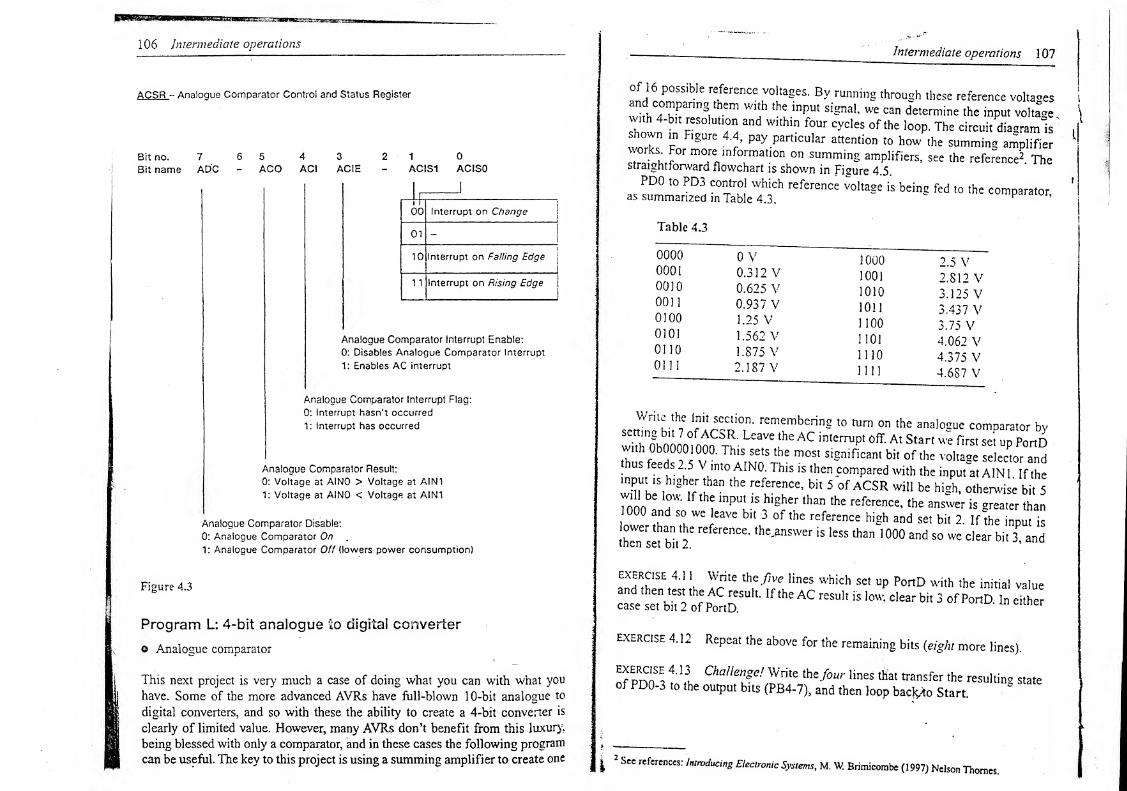
106 Intermediate operations
Analogue Comparator Result:
0: Voltage at AINO > Voltage at AIN1
1: Voltage at AINO < Voltage at AIN1
Analogue Comparator Disable:
0: Analogue Comparator On .
1: Analogue Comparator Off (lowers power consumption)
Figure 4.3
Program L: 4-bit analogue to digital converter
© Analogue comparator
This next project is very much a case of doing what you can with what you
have. Some of the more advanced AVRs have full-blown 10-bit analogue to
digital converters, and so with these the ability to create a 4-bit converter is
clearly of limited value. However, many AVRs don’t benefit from this luxury?
being blessed with only a comparator, and in these cases the following program
can be useful. The key to this project is using a summing amplifier to create one
.Intermediate operations 1 07
fj6mP“Sibie reference voltages. By running through these reference voltages
with 4 hiTrptM t'
6™^ th^.
inPut S1 "na1 ' we can determine the input voltage.w.tn 4-b.t resolution and withm four cycles of the loop. The circuit diaaram is
woT FngUrC
f’
pay.
particular attent'on to how the summing amplifierm°;V
nfTat,0n °n SUmming ampIifiers- the referenced The
straightforward flowchart is shown in Figure 4.5.PDO to PD3 control which reference voltage is being fed to the comparator
as summarized in Table 4.3.H ’
Table 4.3
0 V0.312 V0.625 V0.937 V1.25 V1.562 V1.875 V2.187 V
2.5 V2.812 V3.125 V3.437 V3.75 V4.062 V4.375 V4.687 V
Write the Init section. remembering to turn on the analoaue comparator by
ZmmwmrlU77AC in,ern,p' mAtSan« «”<h ObOOOOlOOO. This sets the most significant bit of the voltaae selector andthus feeds 5 V into AINO. This is then compared with the inputat AIN 1 If the
win be'low IfVh
thC re
?re
uCe> bh 5 °fACSR wiU be hi~2h ’ otherwise bit 5
ml 7 ?,npU
[1S h,gher than the reference
> the answer is greater than
lower thlThr ^ ? °f thC reference hi?h and set bit 2. If the input is
!hw seJbh 2
referenCC - the'answer is less than 1000 and so we clear bit 3, and
EXERCISE 4.1 1 Write the five lines which set up PortD with the initial valnp
««sssr- ,f ,he Ac is * 3
exercise 4. 12 Repeat the above for the remaining bits (eight more lines).
™'SE_4J3
UChallenge! Write thefour lines that transfer the resultino stateof PD0-3 to the output bits (PB4-7), and then loopbac^o Start.
i
2 S“ references: Introducing Electronic Systems, M. W. Brimicombe (1997) Nelson Thornes.
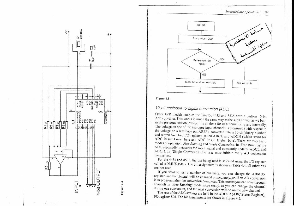
Figure
4.4
Figure 4.5
10-bit analogue to digital conversion (ADC)
Other AVR models such as the Tiny 15, 4433 and 8535 have a built-in 10-bitA/D converter. This works m much the same way as the 4-bit converter we builtin t e previous section, except it is all done for us automatically and internally.
e voltage on one of the analogue input channels is measured (with respect tothe voltage on a reference pin AREF), converted into a 10-bit binarv number,aA
niLSt°red °v
T
er^ 1/0 registers called ADCL and ADCH (which stand forADC Result Lower byte and ADC Result Higher byte). There are two basicmodes of operation: Free Running and Single Conversion. In ‘Free Runnina’ the
a^oePfatdly "ieaSUr£S the input siSnal and constantly updates ADCL andADCH In Single Conversion’ the user must initiate every' AD conversion
For the 4433 and 8535, the
called ADMUX (S07). The bit
are not used.
pin being read is selected using the I/O register
assignment is shown in Table 4.4, all other bits
If you want to test a number of channels, you can change the ADMUXregister, and the channel will be changed immediately, .or, if an AD conversionis m progress, after the conversion completes. This medns you can scan throughchannels m Free Running’ mode more easily, as you can change the channelurtng one conversion, and the next conversion will be on the new channelThe rest of the ADC settings are held in the ADCSR (ADC Status Register),
1/0 register S06. The bit assignments are shown in Figure 4.6.
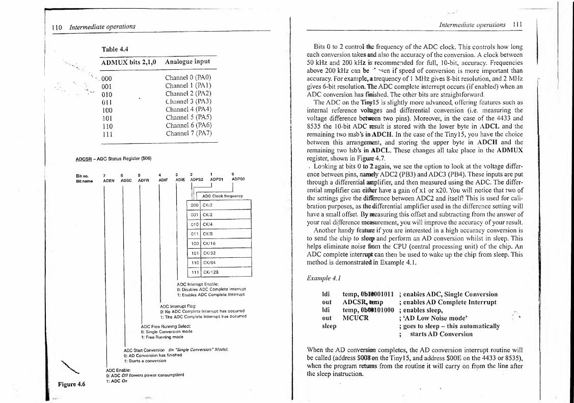
1 1 0 Intermediate operations Intermediate operations 1 1
1
Table 4.4
ADMUX bits 2,1,0 Analogue input
000 Channel 0 (PA0)
001 Channel 1 (PA1)
010 Channel 2 (PA2)
Oil Channel 3 (PA3)
100 Channel 4 (PA4)
101 Channel 5 (PA5)
110 Channel 6 (PA6)
111 Channel 7 (PA7)
ADCSR - ADC Status Register ($06)
Bit no. 7 6 5 4 3 2 1 ®
Bit name ADEN ADSC ADFR ADIF ADIE ADPS2 ADPS1 ADPSO
ADC Clock frequency
000 CK/2
001 CK/2
010 CK/4
Oil CK/8
100 CK/16
101 CK/32
110 CK/64
111 CK/128
ADC Interrupt Enable:
0: Disables ADC Complete Interrupt
t: Enables ADC Complete Interrupt
ADC Interrupt Flag:
0: No ADC Complete Interrupt has occurred
1: The ADC Complete Interrupt has occurred
ADC Free Running Select:
0: Single Conversion mode
1: Free Running mode
ADC Start Conversion OnMSingle Conversion " Mode):
0: AD Conversion has finished
1: Starts a conversion
ADC Enable:
0: ADC Off (lowers power consumption)
1: ADC On
Bits 0 to 2 control tfc frequency of the ADC clock. This controls how long
each conversion takes and also the accuracy of the conversion. A clock between
50 kHz and 200 kHz m recommended for full, 10-bit, accuracy. Frequencies
above 200 kHz can be * ^en if speed of conversion is more important than
accuracy. For example,afrequency of 1 MHz gives 8-bit resolution, and 2 MHzgives 6-bit resolution.TieADC complete interrupt occurs (if enabled) when an
ADC conversion has finished. The other bits are straightforward.
The ADC on the Tinjl5 is slightly more advanced, offering features such as
internal reference vofeges and differential conversion (i.e. measuring the
voltage difference betwen two pins). Moreover, in the case of the 4433 and
8535 the 10-bit ADC result is stored with the lower byte in ADCL and the
remaining two msb’s mADCH. In the case of the Tiny 15, you have the choice
between this arrangement, and storing the upper byte in ADCH and the
remaining two lsb’s in ADCL. These changes all take place in the ADMUXregister, shown in Figure 4.7.
< Looking at bits 0 to 2 again, we see the option to look at the voltage differ-
ence between pins, namely ADC2 (PB3) and ADC3 (PB4). These inputs are put
through a differential amplifier, and then measured using the ADC. The differ-
ential amplifier can either have a gain of xl or x20. You will notice that two of
the settings give the dilfcence between ADC2 and itself! This is used for cali-
bration purposes, as the differential amplifier used in the difference setting will
have a small offset. By measuring this offset and subtracting from the answer of
your real difference measurement, you will improve the accuracy of your result.
Another handy featwif you are interested in a high accuracy conversion is
to send the chip to sleep and perform an AD conversion whilst in sleep. This
helps eliminate noise fam the CPU (central processing unit) of the chip. AnADC complete interrupt can then be used to wake up the chip from sleep. This
method is demonstrate! in Example 4.1.
Example 4.1
ldi temp, ObltOOlOll
out ADCSR, tonpldi temp, ObDtlOlOOO
out MCUCRsleep
; enables ADC, Single Conversion
; enables AD Complete Interrupt
;enables sleep,
;‘AD Low Noise mode 5
;goes to sleep - this automatically
;starts AD Conversion
When the AD conversm completes, the AD conversion interrupt routine will
be called (address $00$ ©n the Tiny 15, and address $00E on the 4433 or 8535),
when the program returns from the routine it will carry on from the line after
the sleep instruction.
Figure 4.6
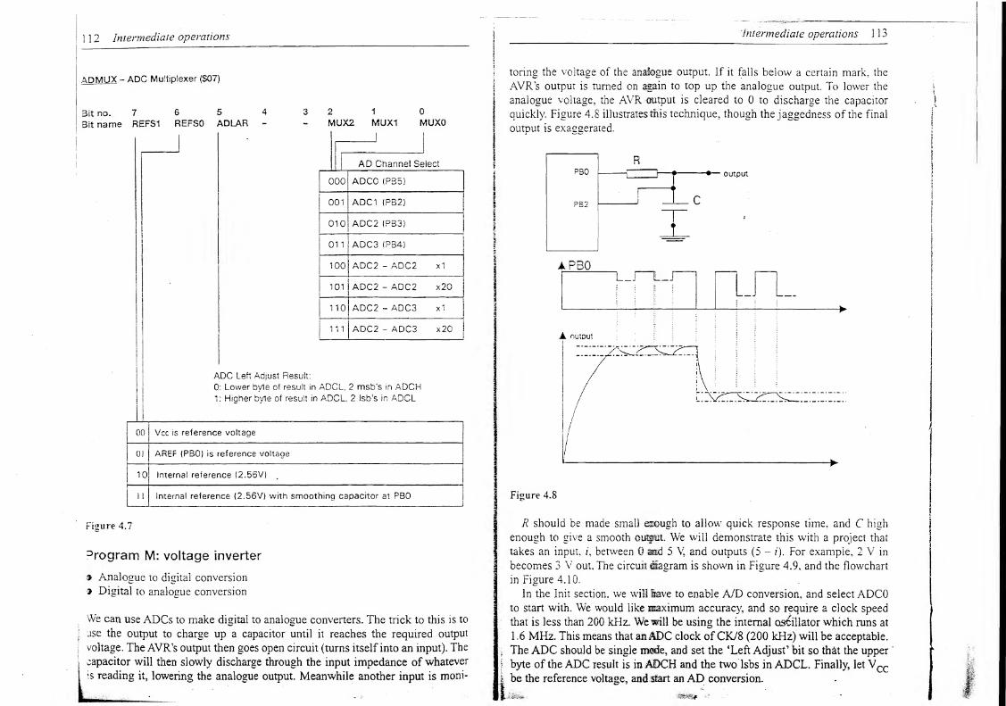
1 1 2 Intermediate operations
ADMUX - ADC Multiplexer ($07)
Bit no. 7 6 5 4 3 2 1 0
Bit name REFS1 REFSO ADLAR - - MUX2 MUX1 MUXO
110! ADC2 - ADC3 xl
111 ADC2 - ADC3 x20
ADC Left Adjust Result:
0: Lower byte of result in ADCL, 2 msb’s in ADCH1 : Higher byte of result in ADCL, 2 Isb’s in ADCL
00 Vcc is reference voltage
0) AREF (PBO) is reference voltage
10 Internal reference (2.56V)
11 Internal reference (2.56V) with smoothing capacitor at PBO
Figure 4.7
Drogram M: voltage inverter
® Analogue to digital conversion
? Digital to analogue conversion
We can use ADCs to make digital to analogue converters. The trick to this is to
\
use the output to charge up a capacitor until it reaches the required output
j
voltage. The AVR’s output then goes open circuit (turns itself into an input). The
j
capacitor will then slowly discharge through the input impedance of whatever
another input is rnoni-i$ reading it, lowering the analogue output. Meanwhile
Intermediate operations 1 1
3
toring the voltage of the analogue output. If it falls below a certain mark, the
AVR’s output is turned on again to top up the analogue output. To lower the
analogue voltage, the AYR etitput is cleared to 0 to discharge the capacitor
quickly. Figure 4.8 illustrates this technique, though the jaggedness of the final
output is exaggerated.
apbo
A output
Figure 4.8
R should be made small enough to allow quick response time, and C high
enough to give a smooth ouiput. We will demonstrate this with a project that
takes an input, /, between 0 -mi 5 V, and outputs (5 - i). For example, 2 V in
becomes 3 V out. The circuit liagram is shown in Figure 4.9, and the flowchart
in Figure 4.10.
in the Init section, we will lave to enable A/D conversion, and select ADCOto start with. We would like maximum accuracy, and so require a clock speed
that is less than 200 kHz. We will be using the internal oscillator which runs at
1 .6 MHz. This means that anADC clock of CK/8 (200 kHz) will be acceptable.
The ADC should be single mode, and set the ‘Left Adjust’ bit so that the upper
byte of the ADC result is inADCH and the two lsbs in ADCL. Finally, let Vccbe die reference voltage, and start an AD conversion.
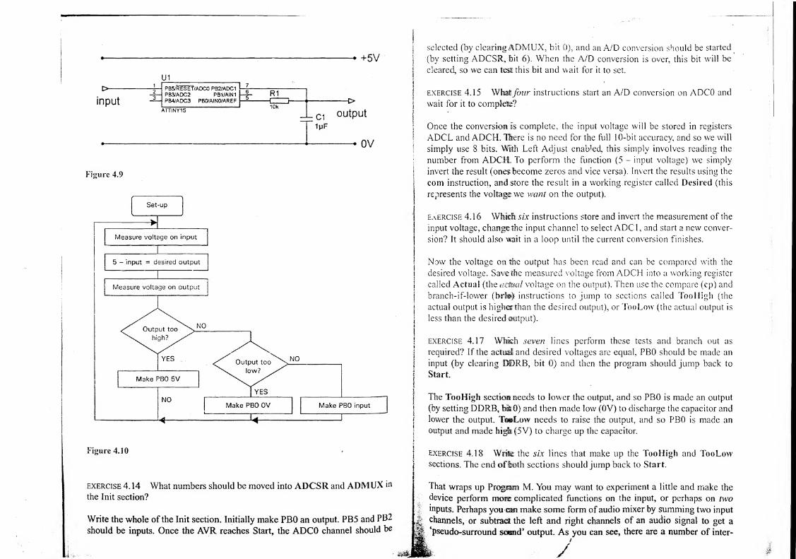
+5V
Figure 4.9
Figure 4.10
exercise 4. 14 What numbers should be moved into ADCSR and ADMUX in
the Init section?
Write the whole of the Init section. Initially make PBO an output. PBS and PB2
should be inputs. Once the AVR reaches Start, the ADCO channel should be
selected (by clearingADMUX, bit 0), and an A/D conversion should be started
(by setting ADCSR, bit 6). When the A/D conversion is over, this bit will be
cleared, so we can test this bit and wait for it to set.
EXERCISE 4.15 Wfa-Afour instructions start an A/D conversion on ADCO and
wait for it to complete?
Once the conversion is complete, the input voltage will be stored in registers
ADCL and ADCH. T&ere is no need for the full 10-bit accuracy, and so we will
! simply use 8 bits. With Left Adjust enabled, this simply involves reading the
number from ADCPL To perform the function (5 - input voltage) we simply
invert the result (ones become zeros and vice versa). Invert the results using the
com instruction, and store the result in a working register called Desired (this
represents the voltage we want on the output).
EaERCISE 4.1 6 Which six instructions store and invert the measurement of the
input voltage, change the input channel to select ADC1, and start a new conver-
sion? It should also wait in a loop until the current conversion finishes.
Now the voltage on the output has been read and can be compared with the
desired voltage. Save the measured voltage from ADCH into a working register
called Actual (the acMal voltage on the output). Then use the compare (cp) and
branch-if-lower (brl») instructions to jump to sections called TooIIigh (the
actual output is higSiarthan the desired output), or TooLow (the actual output is
less than the desired output).
EXERCISE 4.17 Whkh seven lines perform these tests and branch out as
required? If the actml and desired voltages are equal, PBO should be made an
input (by clearing OBRB, bit 0) and then the program should jump back to
Start.
The TooHigh section needs to lower the output, and so PBO is made an output
(by setting DDRB, feitO) and then made low (0V) to discharge the capacitor and
lower the output. T@®Low needs to raise the output, and so PBO is made an
output and made higfb (5V) to charge up the capacitor.
exercise 4.18 Write the six lines that make up the TooHigh and TooLowsections. The end ofloth sections should jump back to Start.
That wraps up Program M. You may want to experiment a little and make the
device perform mom complicated functions on the input, or perhaps on two
inputs. Perhaps you can make some form of audio mixer by summing two input
M channels, or subtract the left and right channels of an audio signal to get a
^^pseudo-surround sound’ output. As you can see, there are a number of inter-
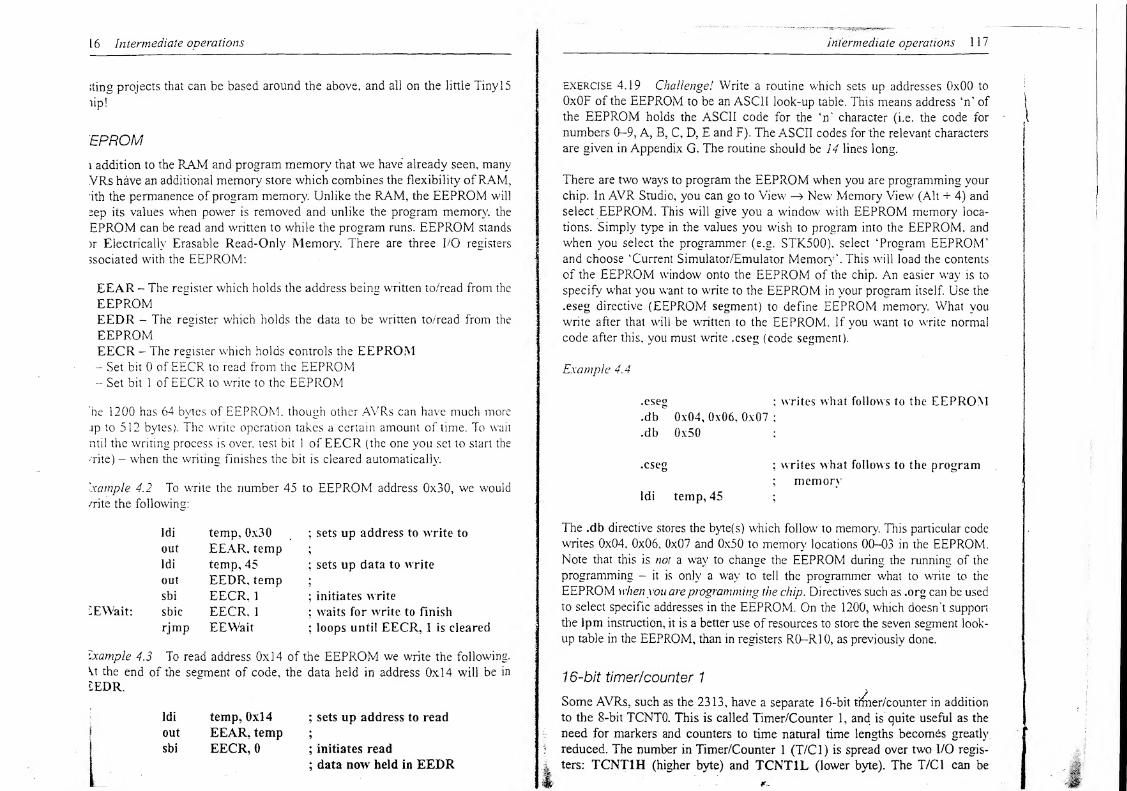
16 Intermediate operations
;ting projects that can be based around the above, and all on the little Tiny 15
lip!
EPROM1 addition to the RAM and program memory that we have already seen, many
VRs have an additional memory store which combines the flexibility ofRAM,ith the permanence of program memory. Unlike the RAM, the EEPROM will
=ep its values when power is removed and unlike the program memory, the
EPROM can be read and written to while the program runs. EEPROM stands
)r Electrically Erasable Read-Only Memory. There are three I/O registers
ssociated with the EEPROM:
EEAR - The register which holds the address being written to/read from the
EEPROMEEDR - The register which holds the data to be written to/read from the
EEPROMEECR - The register which holds controls the EEPROM- Set bit 0 of EECR to read from the EEPROM-- Set bit 1 of EECR to write to the EEPROM
he 1200 has 64 bytes of EEPROM. though other AVRs can have much more
jp to 512 bytes). The write operation takes a certain amount of time. To wait
mil the writing process is over, test bit 1 of EECR (the one you set to start the
rite) - when the writing finishes the bit is cleared automatically.
Example 4.2 To write the number 45 to EEPROM address 0x30, we would
/rite the following:
ldi temp, 0x30 ;sets up address to write to
out EEAR, temp;
ldi temp, 45 ; sets up data to write
out EEDR, temp;
sbi EECR, 1 ;initiates write
CEVVait: sbic EECR, 1 ;waits for write to finish
rjmp EEWait; loops until EECR, 1 is cleared
example 4.3 To read address 0x14 of the EEPROM we write the following.
V the end of the segment of code, the data held in address 0x14 will be in
LEDR.
ldi temp, 0x14; sets up address to read
out EEAR, temp;
sbi EECR, 0 ; initiates read
; data now held in EEDR
Intermediate operations 1 1
7
EXERCISE 4.19 Challenge
!
Write a routine which sets up addresses 0x00 to
OxOF of the EEPROM to be an ASCII look-up table. This means address ‘n’ of |
the EEPROM holds the ASCII code for the ‘m character (i.e. the code for
numbers 0-9, A, B, C, D, E and F). The ASCII codes for the relevant characters
are given in Appendix G. The routine should be 14 lines long.
There are two ways to program the EEPROM when you are programming your
chip. In AVR Studio, you can go to View —> New Memory View (Alt + 4) and
select EEPROM. This will give you a window with EEPROM memory loca-
tions. Simply type in the values you wish to program into the EEPROM, and
when you select the programmer (e.g. STK500). select ‘Program EEPROM’and choose ‘Current Simulator/Emulator Memory’. This will load the contents
of the EEPROM window onto the EEPROM of the chip. An easier way is to
specify what you want to write to the EEPROM in your program itself. Use the
.eseg directive (EEPROM segment) to define EEPROM memory. What you
write after that will be written to the EEPROM. If you want to write normal
code after this, you must write .cseg (code segment).
Example 4.
4
.eseg;writes what follows to the EEPROM
.db 0x04, 0x06, 0x07 ;
.db 0x50
.cseg
ldi temp, 45
The -db directive stores the byte(s) which follow to memory. This particular code
writes 0x04, 0x06, 0x07 and 0x50 to memory locations 00-03 in the EEPROM.Note that this is not a way to change the EEPROM during the running of the
programming - it is only a way to tell the programmer what to write to the
EEPROM whenyou areprogramming the chip. Directives such as .org can be used
to select specific addresses in the EEPROM. On the 1200, which doesn't support
the 1pm instruction, it is a better use of resources to store the seven segment look-
up table in the EEPROM, than in registers RO-R10, as previously done.
16-bit timer/counter 1
Some AVRs, such as the 2313, have a separate 16-bit tfmer/counter in addition
to the 8-bit TCNTO. This is called Timer/Counter 1, and is quite useful as the
need for markers and counters to time natural time lengths becomes greatly
reduced. The number in Timer/Counter 1 (T/Cl) is spread over two I/O regis-
, ters: TCNT1H (higher byte) and TCNT1L (lower byte). The T/Cl can be
;writes what follows to the program
;memory
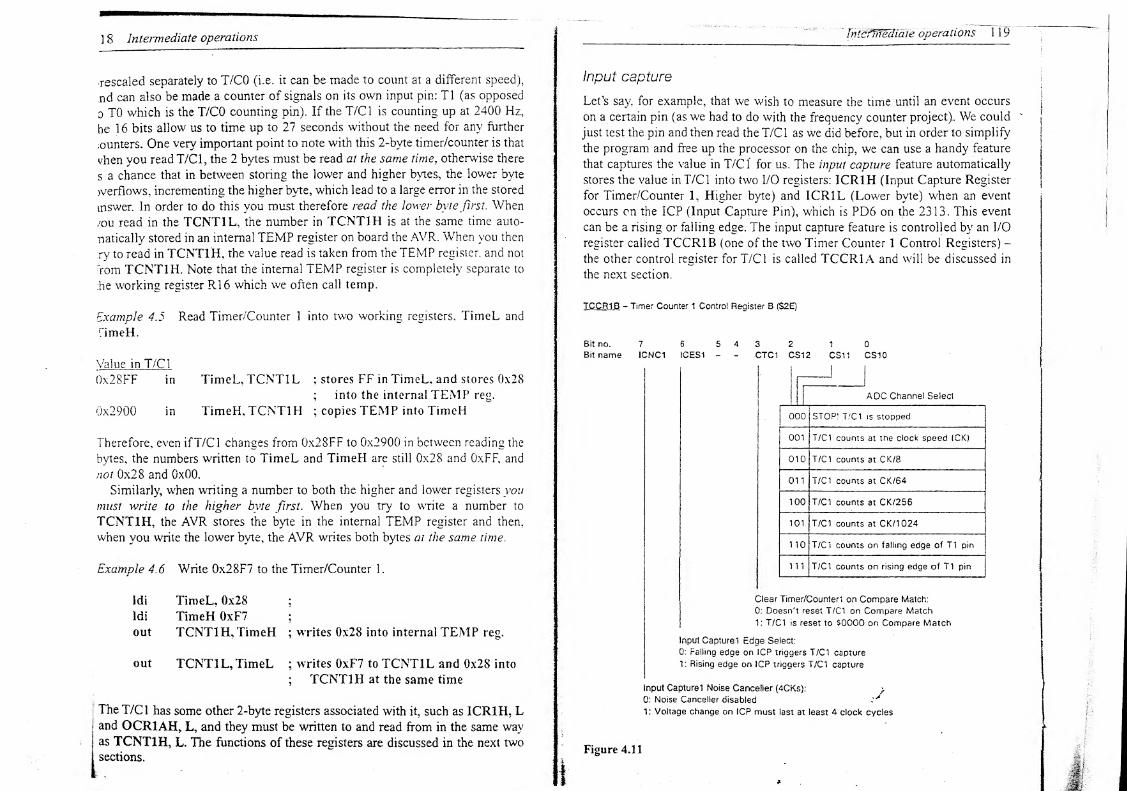
1 8 Intermediate operations
rescaled separately to T/CO (i.e. it can be made to count at a different speed),
nd can also be made a counter of signals on its own input pin: T1 (as opposed
o TO which is the T/CO counting pin). If the T/Cl is counting up at 2400 Hz,
he 16 bits allow us to time up to 27 seconds without the need for any further
:ounters. One very important point to note with this 2-byte timer/counter is that
vhen you read T/Cl, the 2 bytes must be read at the same time,otherwise there
s a chance that in between storing the lower and higher bytes, the lower byte
werfiows, incrementing the higher byte, which lead to a large error in the stored
tnswer. In order to do this you must therefore read the lower byte first. When
iou read in the TCNT1L, the number in TCNT1H is at the same time auto-
-natically stored in an internal TEMP register on board the AVR. When you then
:ry to read in TCNTIH, the value read is taken from the TEMP register, and not
from TCNT1H. Note that the internal TEMP register is completely separate to
he working register R16 which we often call temp.
Example 4.5 Read Timer/Counter 1 into two working registers, TimeL and
TimeH.
Value in T/Cl
0x28FF in TimeL, TCNT1L ; stores FF in TimeL, and stores 0x28
;into the internal TEMP reg.
0x2900 in TimeH, TCNT1H ;copies TEMP into TimeH
Therefore, even ifT/C 1 changes from 0x2SFF to 0x2900 in between reading the
bytes, the numbers written to TimeL and TimeH are still 0x28 and OxFF, and
noi 0x28 and 0x00.
Similarly, when writing a number to both the higher and lower registers you
must write to the higher byte first . When you try to write a number to
TCNT1H, the AVR stores the byte in the internal TEMP register and then,
when you write the lower byte, the AVR writes both bytes at the same time.
Example 4.6 Write 0x28F7 to the Timer/Counter 1.
ldi TimeL, 0x28 ;
ldi TimeH 0xF7 :
out TCNT1H, TimeH ; writes 0x28 into internal TEMP reg.
out TCNTIL, TimeL ; writes 0xF7 to TCNT1L and 0x28 into
;TCNTIH at the same time
f
The T/Cl has some other 2-byte registers associated with it, such as ICR1H, Land OCR1AH, L, and they must be written to and read from in the same wayas TCNTIH, L. The functions of these registers are discussed in the next two
sections.
V ,.-
'^''Jhl&Wediate operations 119
Input capture
Let’s say, for example, that we wish to measure the time until an event occurs
on a certain pin (as we had to do with the frequency counter project). We could
just test the pin and then read the T/Cl as we did before, but in order to simplify
the program and free up the processor on the chip, we can use a handy feature
that captures the value in T/Cl for us. The input capture feature automatically
stores the value in T/Cl into two I/O registers: ICRIH (Input Capture Register
for Timer/Counter 1, Higher byte) and ICR1L (Lower byte) when an event
occurs on the ICP (Input Capture Pin), which is PD6 on the 2313. This event
can be a rising or falling edge. The input capture feature is controlled by an I/O
register called TCCR1B (one of the two Timer Counter 1 Control Registers) -
the other control register for T/Cl is called TCCR1A and will be discussed in
the next section.
TCCR1B - Timer Counter 1 Control Register B ($2E)
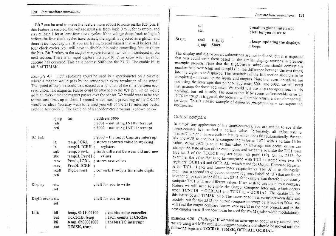
120 Intermediate operations
Bit 7 can be used to make the feature more robust to noise on the ICP pin. If
this feature is enabled, the voltage must rise from logic 0 to 1, for example, and
stay at logic 1 for at least four clock cycles. If the voltage drops back to logic 0
before the four clock cycles have passed, the signal is rejected as a glitch, and
there is no input capture. If you are trying to read signals that will be less than
four clock cycles, you will have to disable this noise cancelling feature (clear
the bit). Bit 3 refers to the output compare function which is introduced in the
next section. There is an input capture interrupt to let us know when an input
capture has occurred. This calls address $003 (on the 2313). The enable bit is
bit 3 of TIMSK.
Example 4.7 Input capturing could be used in a speedometer on a bicycle,
where a magnet would pass by the sensor with every revolution of the wheel.
The speed of the bike could be deduced as a function of the time between each
revolution. The magnetic sensor could be attached to the ICP pin, which would
go high every time the magnet passes over the sensor. We would want to be able
to measure times up to about 1 second which means prescaling of the CK/256
would be ideal. You may wish to remind yourself of the 2313 interrupt vector
table in Appendix E. The skeleton of a speedometer program is shown below:
rjmp Init ; address S000
reti;S001 - not using INTO interrupt
]
I
reti ; S002 - not using INTI interrupt
j
\CJnt: ; $003 - the Input Capture interrupt
in temp, 1CRL;stores captured value in working
in tempH, ICRH;
registers
sub temp, PrevL;finds different between old and new
sbe tempH, PrevH;
values
mov PrevL, ICRL ; stores new values
mov PrevH, ICRHrcall DigConvert ; converts two-byte time into digits
reti
Display: etc. ;left for you to write
! ret
DigConvert: etc. ; left for you to write
ret
Init: Idi temp, Obi 1000100 ; enables noise canceller
out TCCR1B, temp ; T/Cl counts at CK/256ldi temp, 0b00001000 ; enables TC interrupt
out TIMSK, temp ;
/ntermediate operations 1 2
1
rcall Display
rjmp Start
sei; enables global interrupt
v 1
; left for you to write
rcall Display; keeps updating the displays
rjmp Start; ]00ps
Tne display and digit-convert subroutines are not included, but it is expectedthat you could wnte them based on the similar display routines in previousexample projects. Note that the DigConvert subroutine should conven thenumber held over temp and tempH (i.e. the difference between the two times)mto the^digits to be displayed. The remainder o'f the Init section should also beompleted this sets up the inputs and outputs. Note that even thouah we aresing the interrupts that point to addresses S001 and S002 we "still need
instructions for those addresses. We could jus. use nop (no op^ahom i e do
INTfr8!’
bUt retl 1S Safen The ldea 1S that if by Some unforeseeable error anINTO interrupt is triggered, the program will simply return, and no damaae will
unexpected'
15 “ 3^ °f ***** Panting - i.e. expect the
Output compare
In almost any application of the timer/counters, vou are testinc to see if thetimer/counter has reached a certain value. Fortunately, all "chips with a
a^the AVR >n 7 “n"'
1’"" featUre which does this automatically. We can
va^f when tY,°LT
C°Trc the Value in T/C! with a certain 16-bitvalue. When T/Cl is equal to this value, an interrupt can occur, or we can°UtPUI Pr 3nd W^ 3150 makC ^ ^1 reset(see bit j of the TCCR1B register shown on page 119). On the 2313 forexample, the value that is to be compared with T/Cl is stored over two’ I/Omgiste^: OCR1AH and1 OCR1AL (which stand for Output Compare Reeister
.J° fJCl ’ H §h and Lower bytes respectively). The ‘A' is to distinguish
in„,'
rT ““’ll0 le!° "“U! comPare registers (labelled 'B'| thai are found
e TO wta
n „ re
1^f5 1
5
- f»r example, can (herefore consmn.lv
7777T,C * 7° dlfferen ' val“es- if we wish lo use the output compare
Si"- 6 - Tl“ '"“rrt.pt address vanes between differed
wi,l find die output ^mpareZZ’ZgSZZS^fa^n2next chapter we will see how it can be used for PWM (pulse widih modulation).
exercise 4.20 Challenge! If we want an interrupt to occur every second andwe are us,ng a 4 MHz oscillator, suggest numbets °ha, should be m»ed mt ftc^following regtsters: TCCRIB, TIMSK, OCR1AH. OCR1ALI. jr
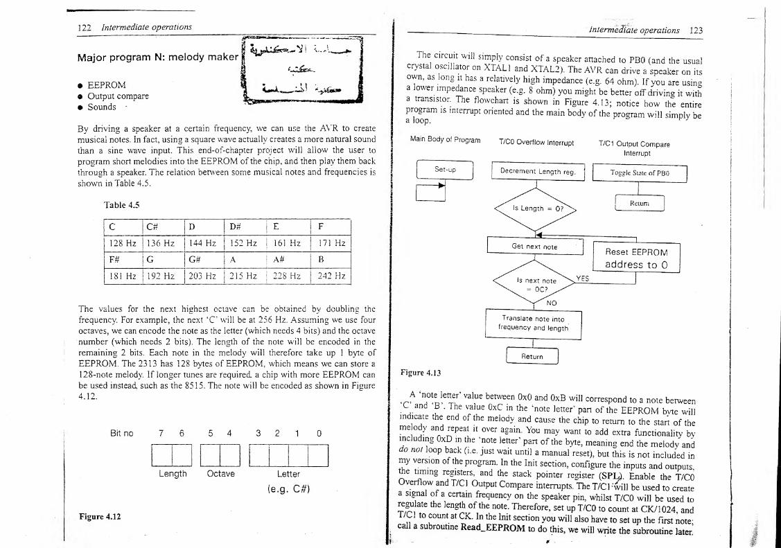
122 Intermediate operations
Major program N: melody maker
• EEPROMe Output compare
• Sounds
By driving a speaker at a certain frequency, we can use the AYR to create
musical notes. In fact, using a square wave actually creates a more natural sound
than a sine wave input. This end-of-chapter project will allow the user to
program short, melodies into the EEPROM of the chip, and then play them back
through a speaker. The relation between some musical notes and frequencies is
shown in Table 4.5.
Table 4.5
The values for the next highest octave can be obtained by doubling the
frequency. For example, the next ‘C will be at 256 Hz. Assuming we use four
octaves, we can encode the note as the letter (which needs 4 bits) and the octave
number (which needs 2 bits). The length of the note will be encoded in the
remaining 2 bits. Each note in the melody will therefore take up 1 byte of
EEPROM. The 2313 has 128 bytes of EEPROM, which means we can store a
128-note melody. If longer tunes are required, a chip with more EEPROM can
be used instead such as the 8515. The note will be encoded as shown in Figure
4.12.
Bit no 7 6 5 4 3 2 1 0
Length Octave Letter
(e.g. C#)
Figure 4.12
intermediate operations
The circuit will simply consist of a speaker attached to PBO (and the usualcrysta osci ator on XTAL1 and XTAL2). The AVR can drive a speaker on itsown, as long it has a relatively high impedance (e.g. 64 ohm). If vou are usinga lower impedance speaker (e.g. 8 ohm) you might be better off driving it witha transistor. The flowchart is shown in Figure 4.13; notice how the entire
abop01 ' S int6ITUpt oriented and the main body of the program will simply be
Main Body of Program t/CO Overflow Interrupt
Decrement Length reg.
T/C1 Output CompareInterrupt
Toggle State of PBO
Figure 4.13
Is Length
Get next note~~]
|
— 1
1
Reset EEPROM
address to 0
<f Is next note \YE$
Translate note into
frequency and length
* ‘
n°YettY value between 0x0 and OxB will correspond to a note between
^and B . The value OxC in the ‘note letter’ part of the EEPROM byte will
indicate the end of the melody and cause the chip to return to the start of themelody and repeat it over again. You may want to add extra functionality bvincluding OxD m the ‘note letter’ part of the byte, meaning end the melody ando not loop back (i.e. just wait until a manual reset), but this is not included inmy version of the program. In the Init section, configure the inputs and outputs,
toe timing registers, and tne stack pointer register (SPL^. Enable the T/COOverflow and T/CI Output Compare interrupts. The T/Cl -will be used to createa signal of a certain frequency on the speaker pin, whilst T/CO will be used toregulate the length of the note. Therefore, set up T/CO to count at CK/1024, andI /Cl to count at CK. In the Init section you will also have to set up toe first note-call a subroutine ReadJSEPROM to do this, we will write the subroutine later!
.24 Intermediate operations Intermediate operations 125
At Start: you need only write one instruction which loops back to Start.
Whenever the T/Cl Output Compare interrupt occurs the output will have to
diange state. This simply involves reading in FortB into temp, inverting it, and
hen outputting it back into PortB.
EXERCISE 4.21 Write the four lines which make up the T/Cl Output Compare
nterrupt section. Include a link to this section at address S004 in the program
nemory.
Ml that remains is the T/CO Overflow interrupt section. Length will be a
working register we use to keep track of the length of the note. At the start of
he section, decrement Length. If it isn’t zero just return; if it is. skip the return
nstruction and carry on. If sufficient time has passed, we need to change the
tote, but first there must be a short pause. This pause allows us to repeat the
>ame note twice without making it sound like a single note played for twice as
ong. An easy way to insert a pause is simply to wait for the T/CO Overflow
interrupt flag to go high again. If it is, skip out of the loop, reset the flag and
move on to the section that reads the next note. Call this section
ReadJEEPROM.
EXERCISE 4.22 Write the eight lines at the start of the T/CO Overflow interrupt
section. Include a link to this section at address S006.
The Read_EEPROM section copies the number in a working register called
address into EEAR. Read the EEPROM into the ZL register, and mask bits
4-7, selecting the ‘note letter’ part of the byte. Then compare ZL with the
number 12 (OxC); if it is equal, jump to a section called Reset. If it isn’t equal
test to see if it is less than 12 (brio). If it isn’t less (i.e. it is greater than 12) it
is an invalid note letter, and so ZL should be reset to 0x0, for want of a better
note. If it is less than 12, skip that instruction.
EXERCISE 4.23 Write the first eight lines of the ReadJEEPROM section.
We wall be using ZL to read values from a look-up table in the program memory(using the 1pm instruction). As you may remember, 1pm uses the byte address
of the program memory, rather than the word address,so we need to multiply
ZL by two (using the lsl instruction). The look-up table will start at word
address 013. We can ensure this using the .org directive in AVR Studio. This
says ‘Let the next instruction be placed at address . . . \ Our look-up table starts
as shown below (.dw is the directive which puts the word or words which follow
in the program memory).
.org 13
.dw 0x7A12 ; frequency for C (word address 013)
.dw 0x7338; frequency for C# (word address 014)
etc.
We must therefore add 26 to ZL to correctly address the look-up table. Use 1pmto read the lower byte, and move the result from R0 into a working registercalled NoteL. Then increment ZL and do the same, moving the result
7into
NoteH.
exercise 4.24 What seven lines perform this task?
We will need to perform some basic maths to derive the values for the look-uptable. Taking the frequencies of the lowest octave to be played shown in Table4.5, and dividing by 4 000 000 (the oscillator frequency) by these values, we geta set of numbers indicating the numbers with which we wish to compare T/Cl.To get higher octaves we will simply divide these values by two. My values areshown in the full version of the program in Appendix J; you may wish to checkthem, or else you can simply copy them.
To get the correct octave we again copy EEDR into temp, swap the nibbles,and then mask bits 2—7. leaving us with the 2 bits we are interested in — thosethat choose the octave. Label the next line GetOctave. First test if the result ofthe AND operation just performed is 0; if it is we can just move on to the nextsection - GetLength. If it isn’t 0, we will divide the number spread over NoteHand NoteL by two, decrement temp, and then loop back to GetOctave.
exercise 4.25 Write the eight lines that use bits 4 and 5 of the EEPROM byteto alter the frequency according to a specified octave.
NoteH and NoteL are now ready to be moved into OCR1AH and OCR1AL,but remember to write the higher byte first. We then read the length, using asimilar method to GetOctave. Again read the EEDR into temp, mask bits 5^0,swap the nibbles, and rotate once to the right. This places the relevant bits in bits1 and 2 of temp. This means the number in temp is 0, 2, 4 or 6. This is almostwhat we want, and by adding 2 to temp we get 2, 4, 6 or 8. This should bemoved into Length.
EXERCISE 4.26 What nine lines make up the GetLength section and returnfrom the subroutine, enabling interrupts.
The program is now finished. By programming different values into theEEPROM when you program the chip, it can be made to*produce any tune. Youmay find a spreadsheet useful in converting notes, octaves and lengths into thehex number which represents them. You may also want' to look into ways toinput bytes to the EEPROM more easily. For example, you could use an arrayof push buttons in a keyboard arrangement, strobing them to lessen the number
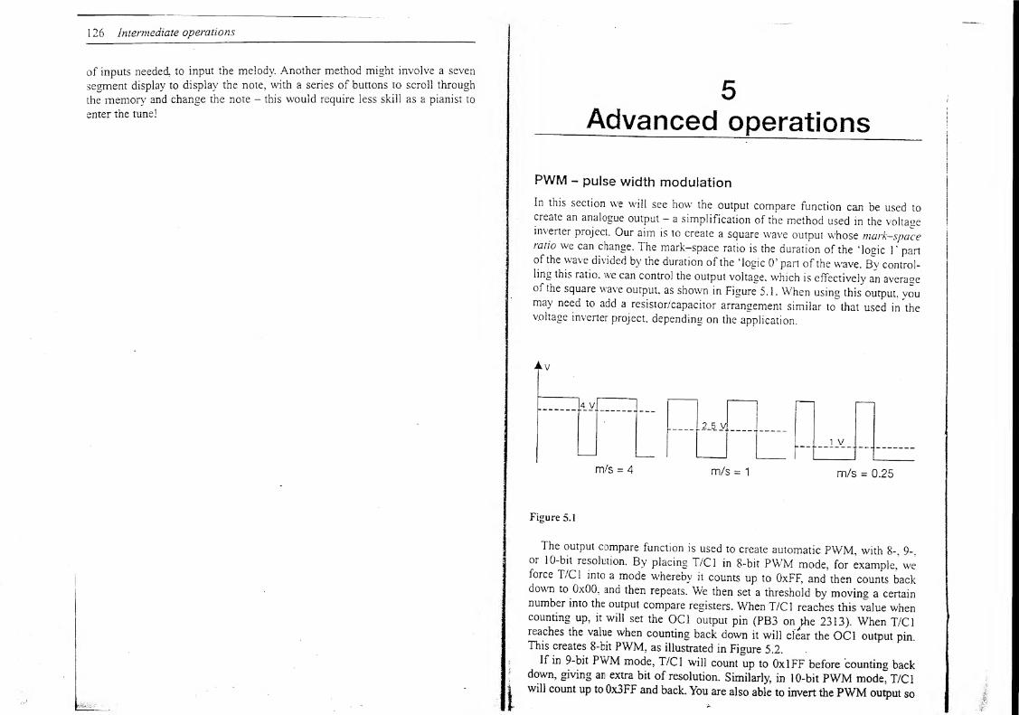
126 Intermediate operations
of inputs needed to input the melody. Another method might involve a seven
segment display to display the note, with a series of buttons to scroll through
the memory and change the note - this would require less skill as a pianist to
enter the tune!
5Advanced operations
PWM - pulse width modulation
In this section we will see how the output compare function can be used tocreate an analogue output - a simplification of the method used in the voltageinverter project. Our aim is to create a square wave output whose mark-spaceratio we can change. The mark-space ratio is the duration of the ‘logic 1' partof the wave divided by the duration of the ‘logic O’ part of the wave. By control-ling this ratio, we can control the output voltage, which is effectively an averageof the square wave output, as shown in Figure 5.1. When using this output, youmay need to add a resistor/capacitor arrangement similar tcTthat used in thevoltage inverter project, depending on the application.
m/s = 4 m/s = 1 m/s = 0.25
Figure 5.1
The output compare function is used to create automatic PWM, with 8-, 9-.
or 10-bit resolution. By placing T/Cl in 8-bit PWTM mode, for example, weforce T/Cl into a mode whereby it counts up to OxFF, and then counts backdown to 0x00, and then repeats. We then set a threshold by moving a certainnumber into the output compare registers. When T/Cl reaches this value whencounting up, it will set the OC1 output pin (PB3 on the 2313). When T/Clreaches the value when counting back down it will clear the OC1 output pinThis creates 8-bit PWM, as illustrated in Figure 5.2.
If in 9-bit PWM mode, T/Cl will count up to OxIFF before counting back
\down
> givin§ ar extra bit of resolution. Similarly, in 10-bit PWM mode, T/Clcount UP *° 0*3FF and back. You are also able to invert the PWM output so
j
!
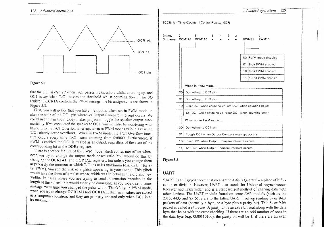
128 Advanced opera tions
0CR1AL
7CNT1L
OCT pin
Figure 5.2
that the OCl is cleared when T/Cl passes the threshold whilst counting up, andOC1 is set when T/Cl passes the threshold whilst counting down. The I/O
register TCCR1A controls the PWM settings, the bit assignments are shown in
Figure 5.3.
First, you will notice that you have the option, when not in PWM mode, to
alter the state of the OC1 pin whenever Output Compare interrupt occurs. Wecould use this in the melody maker project to toggle the speaker output auto-
matically, if we connected the speaker to OC 1 . You may also be wondering whathappens to the T/Cl Overflow interrupt when in PWM mode (as in this case the
T/Cl clearly never overflows). When in PWM mode, the T/Cl Overflow inter-
rupt occurs every time T/Cl starts counting from 0x0000. Furthermore, if
PWM is enabled, the OCl is treated as an output, regardless of the state of the
corresponding bit in the DDRx register.
There is another feature of the PWM mode which comes into effect when-ever you try to change the output mark-space ratio. You would do this bychanging the OCR1AH and OCR1AL registers, but unless you change themat precisely the moment at which T/Cl is at its maximum (e.g. Ox IFF for 9-
bit PWM), you run the risk of a glitch appearing in your output. This glitchwould take the form of a pulse whose width was in between the old and newwidths. In cases where you are trying to send information encoded in thelength of the pulses, this would clearly be damaging, as you would send somegarbage every time you changed the pulse width. Thankfully, in PWM mode,when you try to change OCR1AH and OCR1 AL. their new values are stored
1
a temPorary location, and they are properly updated only when T/Cl is at
I its maximum.
AdvancecLoperations 129
TCCR1A - Timer/Counter 1 Control Register (S2F)
Bit no. 7 6 5 4 3 2 1 0
Bit name COM1A1 COM1AO - PWM 11 PWM10
00 PWM mode disabled
01 8-bit PWM enabled
10 9-bit PWM enabled
11 10-bit PWM enabled
When in PWM mode...
00 Do nothing to OCl pin
01 Do nothing to OCl pin
10 Clear OCl when counting up, sex OCl when counting down
1 1 Set OCl when counting up, dear OCl when counting down
When not in PWM mode...
00 Do nothing to OCl pin
01 Toggle OCl when Output Compare interrupt occurs
10 Clear OCl when Output Compare interrupt occurs
1 1 Set 0C1 when Output Compare interrupt occurs
Figure 5.3
UART
‘UART’ is an Egyptian term that means ‘the Artist's Quarter' - a place of bifur-
cation or division. However, UART also stands for Universal Asynchronous
Receiver and Transmitter, and is a standardized method of sharing data with
other devices. The UART module found on some AVR models (such as the
2313, 4433 and 8515) refers to the latter. UART involve^ sending 8- or 9-bit
packets of data (normally a byte, or a byte plus a parity bit). This 8- or 9-bit
packet is called a character. A parity bit is an extra bit sent.along with the data
byte that helps with the error checking. If there are an odd number 'of ones in
the data byte (e.g. ObOOIlOlOO), the parity bit will be 1, if there are an even
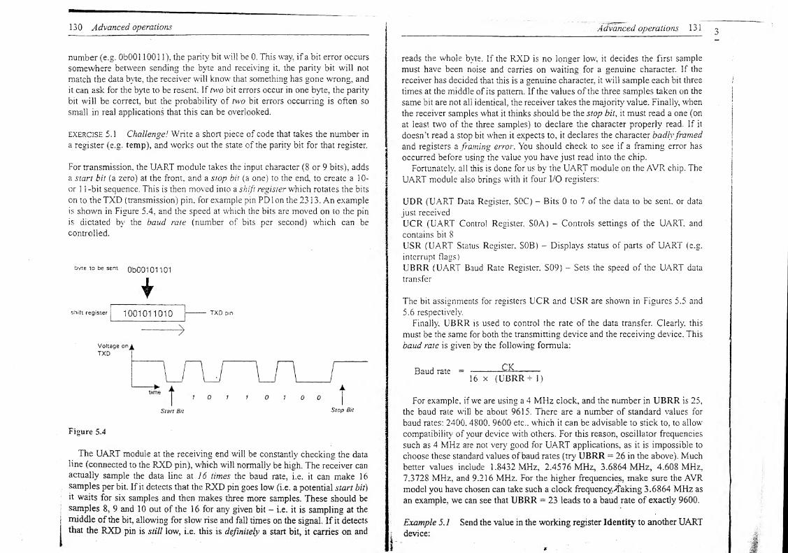
130 Advanced operations
number (e.g. ObOOi 1001 1), the parity bit will be 0. This way, if a bit error occurs
somewhere between sending the byte and receiving it. the parity bit will not
match the data byte, the receiver will know that something has gone wrong, and
it can ask for the byte to be resent. If two bit errors occur in one byte, the parity
bit will be correct, but the probability of two bit errors occurring is often so
small in real applications that this can be overlooked.
exercise 5.1 Challenge! Write a short piece of code that takes the number in
a register (e.g. temp), and works out the state of the parity bit for that register.
For transmission, the UART module takes the input character (8 or 9 bits), adds
a start bit (a zero) at the front, and a stop bit (a one) to the end, to create a 10-
or 1 1 -bit sequence. This is then moved into a shift register which rotates the bits
on to the TXD (transmission) pin. for example pin PD Ion the 23 13. An example
is shown in Figure 5.4, and the speed at which the bits are moved on to the pin
is dictated by the baud rate (number of bits per second) which can be
controlled.
byte to be sent ObOOIOIIOI
I
Voltage
TXD
Start Bit Stop Bit
Figure 5.4
The UART module at the receiving end will be constantly checking the data
line (connected to the RXD pin), which will normally be high. The receiver can
actually sample the data line at 16 times the baud rate, i.e. it can make 16
samples per bit. If it detects that the RXD pin goes low (i.e. a potential start bit)
it waits for six samples and then makes three more samples. These should be
j
samples 8, 9 and 10 out of the 16 for any given bit - i.e. it is sampling at the
middle of the bit, allowing for slow rise and fall times on the signal. If it detects
that the RXD pin is still low, i.e. this is definitely a start bit, it carries on and
Adviced operations 1 3
1
reads the whole byte. If the RXD is no longer low, it decides the first sample
must have been noise and carries on waiting for a genuine character. If the
receiver has decided that this is a genuine character, it will sample each bit three
times at the middle of its pattern. If the values of the three samples taken on the
same bit are not all identical, the receiver takes the majority value. Finally, when
the receiver samples what it thinks should be the stop bit,it must read a one (on
at least two of the three samples) to declare the character properly read. If it
doesn’t read a stop bit when it expects to, it declares the character badlyframed
and registers a framing error . You should check to see if a firaming error has
occurred before using the value you have just read into the chip.
Fortunately all this is done for us by the UART module on the AVR chip. The
UART module also brings with it four I/O registers:
UDR (UART Data Register, S0C) - Bits 0 to 7 of the data to be sent, or data
just received
UCR (UART Control Register, S0A) - Controls settings of the UART. and
contains bit 8
USR (UART Status Register, SOB) - Displays status of parts of UART (e.g.
interrupt flags)
UBRR (UART Baud Rate Register. S09) - Sets the speed of the UART data
transfer
The bit assignments for registers UCR and USR are shown in Figures 5.5 and
5.6 respectively.
Finally UBRR is used to control the rate of the data transfer. Clearly this
must be the same for both the transmitting device and the receiving device. This
baud rate is given by the following formula:
Baud rate = —16 x (UBRR 4- 1)
For example, if we are using a 4 MHz clock, and the number in UBRR is 25,
the baud rate will be about 9615. There are a number of standard values for
baud rates: 2400. 4800. 9600 etc., which it can be advisable to stick to, to allow
compatibility'’ of your device with others. For this reason, oscillator frequencies
such as 4 MHz are not very good for UART applications, as it is impossible to
choose these standard values ofbaud rates (try UBRR — 26 in the above). Muchbetter values include 1.8432 MHz, 2.4576 MHz, 3.6864 MHz, 4.608 MHz,7.3728 MHz, and 9.216 MHz. For the higher frequencies, make sure the AYRmodel you have chosen can take such a clock frequency^Taking 3.6864 MHz as
an example, we can see that UBRR = 23 leads to a baud rate of exactly 9600.
Example 5.7 Send the value in the working register Identity to another UARTdevice:
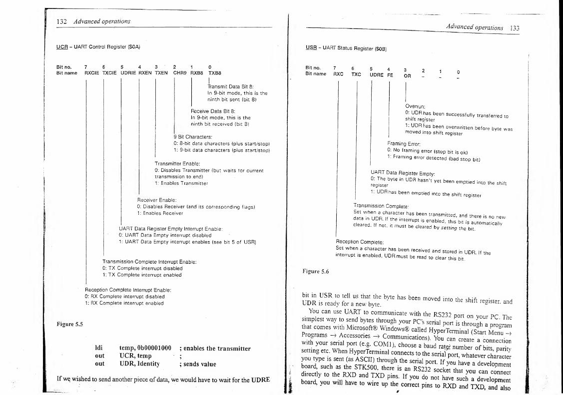
132 Advanced operations
UCR - UART Control Register ($0A)
Bit no.
Bit name7 6 5 4 3 2 1 0
RXCIE TXCIE UDRIE RXEN TXEN CHR9 RXB8 TXB8
Transmit Data Bit 8:
In 9-bit mode, this is the
ninth bit sent (bit 8)
Receive Data Bit 8:
In 9-bit mode, this is the
ninth bit received (bit 8)
9 Bit Characters:
0: 8-bit data characters (plus start/stop)
1: 9-bit data characters (plus start/stop)
Transmitter Enable:
0: Disables Transmitter (but waits tor current
transmission to .end)
1: Enables Transmitter
Receiver Enable:
0: Disables Receiver (and its corresponding flags)
1: Enables Receiver
UART Data Register Empty Interrupt Enable:
0: UART Data Empty interrupt disabled
1: UART Data Empty interrupt enables (see bit 5 of USR)
Transmission Complete Interrupt Enable:
0: TX Complete interrupt disabled
1: TX Complete interrupt enabled
Reception Complete Interrupt Enable:
0: RX Complete interrupt disabled
1: RX Complete interrupt enabled
Figure 5.5
temp, ObOOOOlOOO; enables the transmitter
UCR, temp;
UDR, Identity; sends value
Ifwe wished to send another piece of data, we would have to wait for the UDRE
Advanced operations 132
USR - UART Status Register ($0B)
Bit no. 7 6 543Bit name RXC TXC UDRE FE OR
Overrun:
°: UDRhcis been successfully transferred toshift register
1: UDR has been overwritten before byte wasmoved into shift register
Framing Error:
0: No framing error (stop bit is ok)1: Framing error detected (bad stop bit)
UART Data Register Empty
register^'
6 ^ haSn '
t ^ bee" em?tied *"«> the shift
1: UDR has been emptied into the shift register
Transmission Complete:
d
S
a«7nh
UDRC
5XCt
mhaS^ Uans™ed ' *nd there is no new
cleared 1 > TUP1 * enabled' Th,s blt « automaticallycleared. If not, it must be cleared by setting the bit.
Reception Complete:
Set when a character has been received and stored in UDR If theinterrupt ,s enabled, UDR must be read to clear this bit.
’
Figure 5.6
UDR S b>S *“ *« register, and
siJplesf™: yl“
PC ""thar comes with Microsoft* Windows® called HypetferminaUSan M
'
Programs Accessories -o Communications!Mcnu -*
with your serial per, ,e.g. COM,,. ch*L™, STSSsetting etc. When HyperTerminal connects to the serial^orp rMratever chaacteryou type is sent (as ASCII) throuah the serial nort If1 "I ,
boar<t such as .he STK500. there *directlv rn the rytt <na Tvn • ,r ,
socket that y°u can connect
\ ...T®and TXD p,ns - If y°u do not have such a developmentboard, you will have to wire up the correct pins to RXD and TXD, and also
1 34 Advanced operations
make sure the voltaae (which could be anywhere between 3 and 12 V), is regu-
lated to a safe voltage (like 5 V). Figure 5.7 shows how to wire up the pins on
a 9-pin RS232 socket to allow direct communication with the AVR. Some of the
other pins are handshaking pins, which can be bypassed by connecting them
together as shown.
' Ground
Transmit (i.e. connect to RXD pin of AVR)
Receive (i.e. connect to TXD pin of AVR)
Figure 5.7
COM1
CONN-D9
Program 0: keyboard converter
» UARTa Sounds
% Seven segment displays
% Output compare
We can use HyperTermina! to send characters to our melody maker project, via
rhe UART module. We can effectively convert our computer keyboard into a
musical keyboard by assigning note frequencies to the different characters. For
example, when 1 press the letter ‘a’ when HyperTerminal is connected to the
AVR, it will send ‘a’ to the UART module. This can then trigger an interrupt,
eonvert the ASCII code for ‘a’ into the frequency for a ‘C note. I have arranged
my keys on the keyboard so that they resemble how they are arranged on a
piano, but you may"find you can fit more notes if you arrange them differently.
Figure 5.8 shows my arrangement.
Figure 5.8
'Advanced operations 135
We will also use a seven segment display to show which note is being played;
this can help overcome any user confusion over how the letters on the computer
keyboard correspond to the musical notes. There will be a separate LED to
show the sharp symbol (#). The circuit diagram is shown in Figure 5.9, and the
flowchart in Figure 5.10.
In the Init section, set up inputs and outputs and set OCi to toggle with every
output compare (this handles the speaker output for us, so there is no need to
write a routine for the Output Compare interrupt). Make all other timer settings
the same as in the melody maker, choose a baud rate of 9600, and enable the
UART receiver and the UART Receive Complete interrupt.
Again, the main body of the program is just a constant loop to Start. The
UART Receive Complete interrupt tells us that some new data has been
received on the line, which we should convert to a frequency and then change
OCR1AH and OCR1AL accordingly. The beginning of the interrupt routine
should therefore read UDR into ZL. The ASCII conversion table is shown in
Appendix G. I will only use letters a-z. all lower case, which correspond to
0x61 to 0x7A in ASCII, so subtract 0x61 from ZL to get a number between 0
and 25. If ZL is more than 25, an inappropriate key is being pressed, so move26 into it. this ensures no matter what character we read the program will stay
within the look-up table we are about to write. Now multiply ZL by two to
make it a word address. We wish to read the program memory into RO, using
the 1pm instruction, and then copy R0 into OCR1AH. and OCR1AL. We can
do this directly (i.e. without having to play with octaves etc., so we don’t need
NoteH and NoteL). However, when doing this directly, we have to remember
the golden rule - you must write the higher byte first. There are two ways of
doing this. First, arrange the data in the look-up table so that the higher byte
actually comes first. For example, if I wished the number 0xlE84 to be the
code for a ‘C note, the top of my look-up table would be:
•dw 0x841E
This is a little confusing, and an easier way is to start by pointing ZL to the
higher byte. In other words, if the table starts at byte address 26 in the program
memory, add 27 to ZL instead of 26, to point ZL to the higher bytes. Then to
read the lower byte, decrement ZL.
EXERCISE 5.2 Challenge
!
Write the first 12 lines of the UART Receive
Complete interrupt section which use the data received by the UART module to
write new values for OCR1AH and OCR1AL.,/
For the display we have another look-up table, below the first, starting at word
address 43. We can simply add 60 (30 x 2) to ZL to point to the second look-
up table. This holds the seven segment codes for the note letters. Bit 3 will be
used to light up the # (sharp) LED.
*
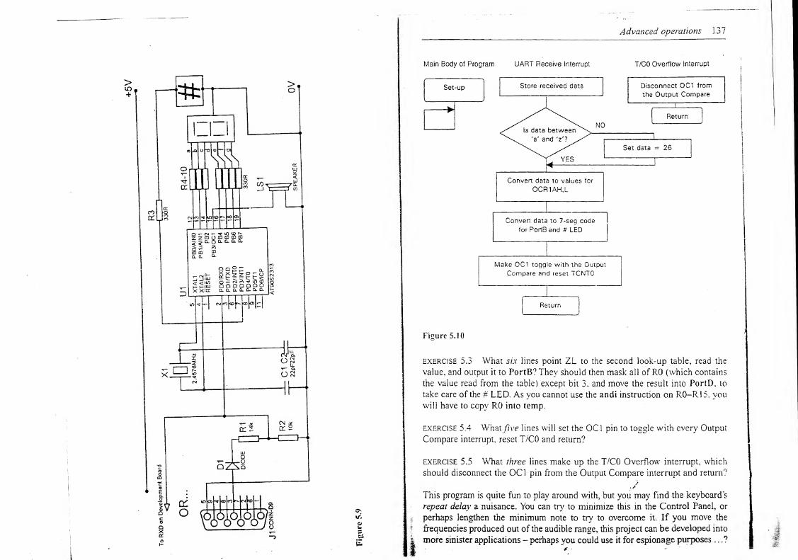
Figure
5.9
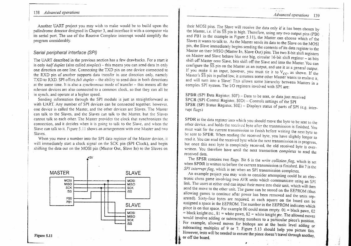
1 38 Advanced operations
Another UART project you may wish to make would be to build upon the
palindrome detector designed in Chapter 3, and interface it with a computer via
its serial port. The use of the Receive Complete interrupt would simplify the
program considerably.
Serial peripheral interface (SPI)
The UART described in the previous section has a few drawbacks. For a start it
is only halfduplex (also called simplex) - this means you can send data in only
one direction on one line. Connecting the TXD pin on one device connected to
the RXD pin of another supports data transfer in one direction only, namely
TXD to RXD. SPI offers full duplex - the ability to send data in both directions
at the same time. It is also a synchronous mode of transfer - this means all the
relevant devices are also connected to a common clock, so that they can all be
in synch, and operate at a higher speed.
Sending information through the SPI module is just as straightforward as
with UART. Any number of SPI devices can be connected together; however,
one device is called the Master, and the other devices are Slaves. The Master
can talk to the Slaves, and the Slaves can talk to the Master, but the Slaves
cannot talk to each other. The Master provides the clock that synchronizes the
connection, and it decides when it is going to talk to the Slave, and when the
Slave can talk to it. Figure 5. 1 1 shows an arrangement with one Master and two
Slaves.
When you move a number into the SPI data register of the Master device, it
will immediately start a clock signal on the SCK pin (SPI Clock), and begin
shifting the data out on the MOSI pin (Master Out, Slave In) to the Slaves on
Figure 5.11
Advanced operations 1 39
;l;
ei
LM0SI pmS
,TheJlaVewili reCe 'Ve the data on! >' if jt has been chosen bv
mSer
’
'tZ
lf
^ Pm 'S hlgn'
J
herefore’ usinS any^ output pins (PBOnd PB1 in the example m Figure 5.11), the Master can choose which of the
Slaves it wants to talk to. As the Master sends its data to the Slave on the MOSIpin, the Slave immediately begins sending the contents of its data register to theMaster on their M1SO (Master In, Slave Out) pins. The two 8-bit shift registers°" Ma^rand SIave behave llke one big, circular 16-bit shift register - as bitsshift off Master_onto Slave, bits shift off the Slave and into the Master You canconfigure the SS pin on the Master as an output, and use it as a general output.If you make it an input, however, you must tie it to Vcc , as'shown. If theMaster's SS pin is pulled low, it assumes some other Master wants to enslave itand will turn into a Slave! This allows some hierarchy between Masters in acomplex SPI system. The I/O registers involved with SPI are:
SPDR (SP! Data Register, SOF) - Data to be sent, or data just receivedSPCR (SPI Control Register. SOD ) - Controls settings of the SPISPSR (SPI Status Register, SOE) - Displays status of parts of SPI (e o interrupt flags)
s ' cr'
SPDR is the data register into which you should move the byte to be sent to theother device, and holds the received byte after the transmission is finished Youmust wait for the current transmission to finish before writing the next byte tobe sent to SPDR. When reading the received byte, you have slightly longer toread it. You can read the received byte while the next transmission is in progressbut once this next byte is completely received, the old received byte is over-written You therefore have until the next transaction completes to read thereceived data.
1C
The SPSR contains two flags. Bit 6 is the write collision flag, which is setwhen SPDR is written to before the current transmission is finished. Bit 7 is theSPi interrupt flag, which is set when an SPI transmission completes.An example project you may wish to consider attempting could be an elec-
tronic chess game involving two AVR units which communicate using an SPIlink The users at either end can input their move into their unit, which will thensend the move to the other unit. The game can be stored on the EEPROM fthusallowing games to continue after power has been removed and the units sep-arated) Sixty-four bytes are required, as each square on the board can beassigned a space in the EEPROM. The number in the EEPROM indicates whichpiece is on that space. For example 00 could mean empty. 01 = black pawn (Pbiack knight etc., 8 1 = white pawn, 82 = white knight j*c. The allowed moveswould involve adding or subtracting numbers to a particular piece’s position
For example, allowed moves for bishops are at the basic level adding orsubtracting multiples of 9 or 7. Figure 5.13 should help you picture this.However, tests will be needed to ensure the piece doesn’t travel through anotheror off the board.
° ->
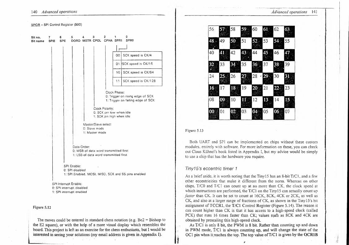
140 Advanced operations
Figure 5.12
The moves could be entered in standard chess notation (e.g. Be2 = Bishop to
ithe E2 square), or with the help of a more visual display which resembles the
|
board. This project is left as an exercise for the chess enthusiasts, but 1 would be
interested in seeing your solutions (my email address is given in Appendix I).
Advanced operations 1 4
1
Figure 5.13
Both UART and SPI can be implemented on chips without these custom
modules, entirely with software. For more information on these, you can check
out Claus KuhneFs book listed in Appendix I, but my advice would be simply
to use a chip that has the hardware you require.
TinylS’s eccentric timer 1
As a brief aside, it is worth noting that the TinylS has an 8-bit T/Cl, and a few
other eccentricities that make it different from the norm. Whereas on other
chips. T/CO and T/Cl can count up at no more than CK, the clock speed at
which instructions are performed, the T/Cl on the Tiny 15 can actually count up
faster than CK. It can be set to count at 16CK, 8CK, 4CK or 2CK, as well as
CK. and also at a larger range of fractions of CK, as shown in the TinylS’s bit
assignment of TCCR1, the T/Cl Control Register (Figure 5.14). The reason it
can count higher than CK is that it has access to a high-speed clock (called
PCK) that runs 16 times faster than CK; values such as 8CK and 4CK are
obtained by prescaling this high-speed clock.
As T/Cl is only 8 bit, the PWM is 8 bit. Rather than counting up and down
in PWM mode, T/Cl is always counting up, and will change the state of the
OC1 pin when it reaches the top. The top value ofT/Cl is given by the QCR1B
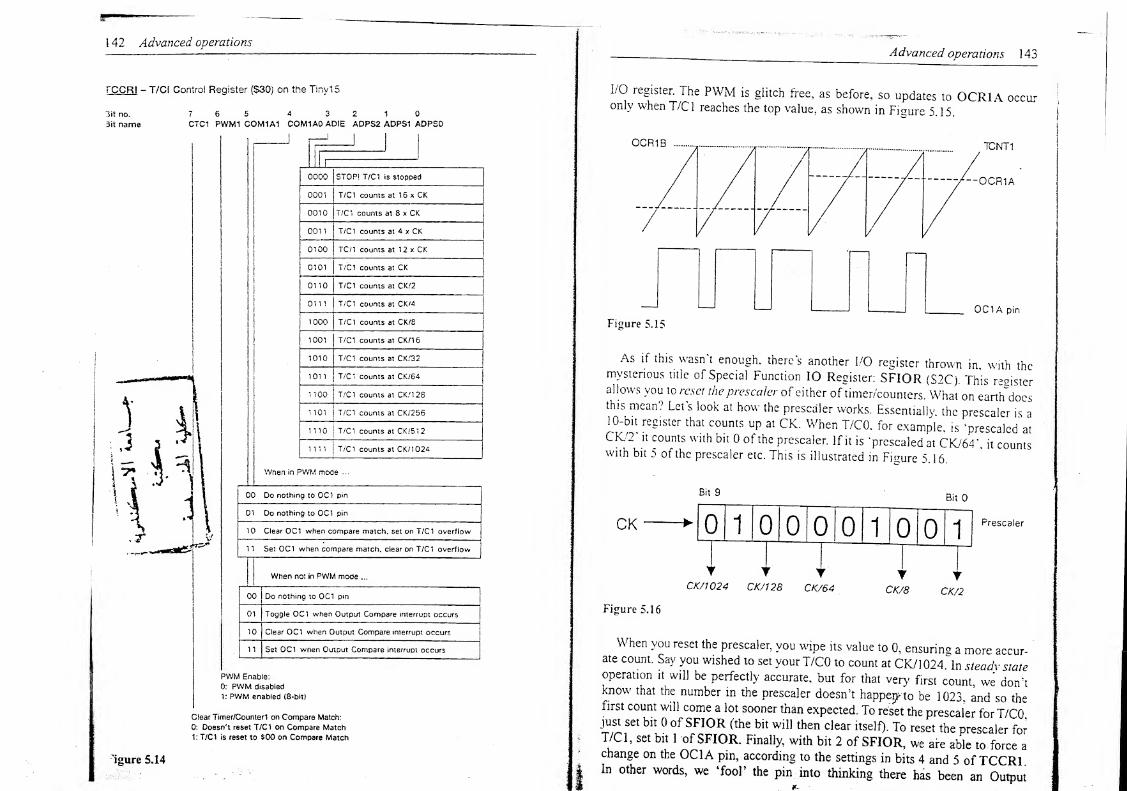
1 42 Advanced operations
TCCRl - T/CI Control Register ($30) on the Tiny15
7 6 5 4 3 2 1 0
CTC1 PWM1 COM1A1 COM1AO ADIE ADPS2 ADPS1 ADPSO
mi
0000 STOP! T/CI is stopped
0001 T/CI counts at 16 x CK
0010 T/CI counts at 8 x CK
0011 T/CI counts at 4 x CK
0100 TC/1 counts at 12 x CK
0101 T/CI counts at CK
0110 T/Cl counts at CK/2
0111 T/CI counts at CK/4
1000 T/CI counts at CK/8
1001 T/CI counts at CK/1
6
1010 T/CI counts at CK/32
1011 T/CI counts at CK/64
1 TOO T/CI counts at CK/1 28
1101 T/CI counts at CK/256
1110 T/CI counts at CK/5 12
nil T/CI counts at CK/1 024
When in PWM mode ...
Do nothing to OC1 pin
Do nothing to OC1 pin
Clear OC1 when compare match, set on T/CI overflow
Set OC1 when compare match, clear on T/Cl overflow
When not in PWM mode ...
) Do nothing to 0C1 pin
Toggle OC1 when Output Compare interrupt occurs
) Clear OC1 when Output Compare interrupt occurs
Set OC1 when Output Compare interrupt occurs
PWM Enable:
0: PWM disabled
1: PWM enabled (8-bit)
Clear Timer/Counterl on Compare Match:
0: Doesn't reset T/CI on Compare Match1: T/CI is reset to $00 on Compare Match
Igure 5.14
Advanced operations 143
I/O register. The PWM is glitch free, as before, so updates to OCR1A occuronly when T/Cl reaches the top value, as shown in Figure 5.15.
OCR1A
0C1 A pin
Figure 5.15
As if this wasn't enough, there's another I/O register thrown in, with themysterious title of Special Function 10 Register: SFIOR (S2C). This registerallows you to reset the prescaler of either of timer/counters. What on earthdocsthis mean? Let's look at how the prescaler works. Essentially, the prescaler is a10-bit register that counts up at CK. When T/CO. for example, is ‘prescaled atCK/2 it counts with bit 0 of the prescaler. If it is ‘prescaled at CK/64’. it countswith bit 5 of the prescaler etc. This is illustrated in Figure 5. 1 6.
0 1 0 0 0 0 1 0 OilPrescaler
Figure 5.16
Y Y TCK/1024 CK/128 CK/64
When you reset the prescaler, you wipe its value to 0, ensuring a more accur-ate count. Say you wished to set your T/CO to count at CK/1024. In steady stateoperation it will be perfectly accurate, but for that very- first count, we don’tknow that the number in the prescaler doesn’t happeiy to be 1023, and so thefirst count will come a lot sooner than expected. To reset the prescaler for T/COjust set bit 0 of SFIOR (the bit will then clear itself). To reset the prescaler forT/Cl, set bit 1 of SFIOR. Finally, with bit 2 of SFIOR, we are able to force achange on the OC1A pin, according to the settings in bits 4 and 5 of TCCRl.In other words, we ‘fool’ the pin into thinking there has been an Output
1 44 Advanced operations
Compare Match; however there is no interrupt generated and T/Cl will not
reset.
Although at the time of publication, the Tiny 15 was the only model with this
type of T/Cl, we can expect that other models of AYR will emerge with a
similar T/Cl.
Shrtcts
There are a number of ways to trim down your program into a slender and
seductive beauty. One of the easiest ways is to use the .macro assembler direc-
tive. This allows you to, in effect, create your own instructions.
Example 5.7 At the top of your program ...
.macro nopnop ; the name of this macro is nopnop
rjmp POl.endmacro
Then, in the rest of your program, you can write the instruction nopnop. and
the assembler will interpret this as rjmp PCM-1. Why have I called this
nopnop? Jumping to the next line with the rjmp instruction wastes nw clock
cycles, as the rjmp instruction takes twice as long as most instructions. Writing
rjmp POl is therefore equivalent to writing two nops. but only takes up
one instruction. Macros can also be given operands, which are referred to as
720, @1 etc.
|
Example 5.2
.macro multiply ; the name of this macro is multiply
mov temp, @0clr @0 , wipes answer register
tst @1 ; tests multplier
breq PC+4! add @0, temp ;
adds multiplicand to itself
dec @1rjmp PC-4 ;
repeats
I .endmacro
In the program, ifwe wanted to multiply the number in Seconds by the number
in Counter, we could simply write:
multiply Seconds, Counter
Mote that we can use labels in the macro, these will immediately be translated
as relative jumps, and so there will be no risk of label duplication should the
macro be used more than once in the program.
Advanced operations 1 4
5
™oflag isST"8 maCI° Ca"'d S,“’ Wh,ch sk‘Ps ”« instruction if
Reregister goes' high .
&*"* * N« in an
macrosPMac
n
rLt0
are
a
simp!J ways XT™' “fcode into neat one-word actions TV •„* ' p tty Pieces of
program will end up just as long (ta you will s^Te e™dX “ y°“r
Using subroutines will actually make vnnr nm„ lexpanded version),
space in the program memory! BUT mav XfXe I
" " “ke “p Iess
instruction takes three clock cycles and tV rPt•
0ng5 to run. The rcall
subroutines are „,em„, a ^ “
A Mega summary
Covering the cornucopia of new functions found on the Me^aAVR nnoone of the aims of this book It is worth i,., .
iviesaA\ K range is not
that you can at least decide whether it s worth^’S ’VlnS 3 bnef intr°duction so
they offer more of what ,oo ve see soTr1“™?® m°,C “h0"' ,hem - Rra
ADCs, more VO pins, more memo^dmXXS~ ~^'rdZrr xsrsx Th"e -which performs multiplication in two
bnilt hard"',re
to multiply two registers toiethe” rX. I Pf ‘"sTucnon is used
unsigned/fractional etc.) are als'o available TteXlXd' him ‘''“T
1 *sisned/
direct calls and jumps respectively The onlv diffi.
dJ,
P Instructl0ns are
.0 jump to, or eali,X pa! .f ^ence thts I,nutation on non-Mega AVRs unless yo'uThe new instructions also include additions to L 3 g Pro°rams -
most notable is the stm instruction. This stores theIT' ,nsm,ctions.
into the program memory. Th,s ”* R '
IS a way for the AVR to send the entire contents^ !
tacilltate debuggmg. It
registers, SRAM) to a PC. so that von nan ultS
.
re"isters d/0, working
in your circuit board. .
SeC ^ at S on inside it as it runs
Final program P: computer controlled robot• Serial communication• PWM to drive a motor• Seven segment display to display messages
'
1 46 Advanced operations
A computer controlled robot has been chosen as a fun project which ties together
some of the topics discussed in the book. The project that will be developed will
be a skeleton, around which a semi-intelligent robot can be based. We can send
commands to the robot through the serial port on the computer to the UARTmodule on the AVR. Motor speed can be controlled through the use ofPWM, and
a seven segment display will be used to show messages, and allow the robot to
‘talk’. The use of EEPROM to store moves and the application of the music
modules are some basic enhancements that could be added on. Sensors could be
placed on the robot, and it could send information back to the computer regarding
the states of these sensors. More sophisticated software on the computer end
which would make the robot behave like a state machine and respond to various
inputs, would be a more interesting development, but this goes beyond the scope
of this book. The circuit diagram of the basic robot is shown in Figure 5.17.
Both motors are driven from the OC1 pin, which is the output of the PWM.To allow the robot to turn, the left motor can be turned off by setting the PD2pin. This means it can turn in one direction only, but still gives it plenty of
freedom. A larger AVR, such as the 8515, has two PWM outputs, on OC 1 A and
OC1B pins. This means the motors can be driven independently.
The commands we can send the robot are shown in Table 5.1.
Table 5.1
Letter ASCII Function Message to PC
a& 0x67 Go/Stop ‘Go’ or ‘Stop’
t 0x74 Begin turning or end turning
(stop/start left motor) ‘Turning’
+ 0x2B Speed up ‘Speeding up’
- 0x2D Slow down ‘Slowing down’
s 0x73 Change speed
(followed by two-digit number, e.g. s25) ‘Speed set to ...’
[ 0x5B Begin message
(to be displayed on seven segment displays) <message>
] 0x5D End message
All other inputs will be ignored. The robot will send the computer back
confirmations of each action. For example, if it is sent a ‘t\ it will reply with
‘Turning’. Not all letters can be displayed on the seven segment displays - to be
able to display any letter we need a more complex display (e.g. a 14 segment
display). As it is, we are unable to display letters k, m, q, v, w and x.
The structure of the program is very straightforward, and entirely interrupt
driven. Ifa receive interrupt occurs, the program identifies the character received
and responds accordingly. To simplify the Display subroutine, we can make this
R14
R13
Figure
5.17
1 48 Advanced operations
driven by T/CO, such that every time T/CO overflows, the Display subroutine is
called. This not only removes the burden on us of remembering to call it regu-
larly, but also means we can remove the counter register that allows the entire
subroutine to be executed only once every 50 visits. We must therefore configure
T/CO so that it overflows sufficiently often. The refresh rate should be more than
25 times a second and, bearing in mind there are four displays, this means the
Display subroutine should be called at least 100 times a second. As T/CO over-
flows after 256 counts, this means a minimum T/CO rate of 25.6 kHz. If we are
using a 2.4576 MHz crystal, this represents prescaling of CK/64.
In the lnit section, configure the inputs and outputs, and T/CO. Set up T/Cl
to count at CK. set OC1 to clear when T/Cl passes the threshold counting up.
and set when T/Cl passes it coming down (this means the higher the number in
OC1AH/L, the faster the speed of the motor). Disable PWM for the time being
(8-bit PWM will be enabled when a ‘g’ is received from the computer). Don't
forget to set up the stack pointer I/O registers. On the 2313 this is just SPL. and
which you should load with ‘RAMEND'. Enable the Receive Complete UARTInterrupt, and enable the Receive Mode. Set the UART baud rate to 9600. and
enable the global interrupt bit.
Adjust the Display subroutine from previous projects to include four
displays. The seven segment code to be displayed will be stored in registers
R21-24. Note that as these will hold the seven segment code, their values can
be moved directly into PortB.
exercise 5.8 Make the necessary changes to create a Display subroutine for
this program.
The Receive Complete Interrupt should first test to see if what is being sent is
to be taken as a command, or as part of a text message. The T bit will be used
to indicate which interpretation is appropriate (i.e. the start message command*[* will set the T bit. and the end message command ‘f will clear it. It should
also be cleared in the lnit section. The Receive Complete Interrupt section
should start by testing for an end message symbol, and jump to EndMessage if
it is received. The next test should be the T bit. if it is set we should branch to
Message. The other symbols (g, t. s, -) can be tested in any order, though it
is simplest to put the test for ‘[’ at the end. If it is the T bit should be set.
Any other symbol should be ignored.
The Turning section should toggle the state of the PD2 pin (which controls
the left motor). The receive mode should then be disabled, and the transmit
mode enabled. Move the ASCII code for a T' into temp, and then call a subrou-
tine called Send. This subroutine will take the number in temp and send it
through the UART module; we will write the subroutine later. Repeat the above
for the rest of the letters. We also need to send a new line (also called line feed)
and carriage return symbol, so that each message sent to the PC appears on a
new line. These symbols are OxOA and OxOD respectively, but these will be
Advanced operations 149
common to all messages, so at this point (after sending the ‘g’), just branch to
EndMessage, which will do the rest.
EndMessage will clear the T bit,,send OxOA and OxOD to the PC, and then
disable the transmit mode and enable the receive mode.The Send subroutine should put the contents oftemp into the UDR, and then
enter a loop in which it constantly checks the transmit complete flag (the TXCbit in USR). You must not write to UDR in this loop (i.e. loop to Send+1, andnot to Send), because this resets the TXC flag, which means you will stay in the
loop forever. After the TXC flag goes high, you must reset it by setting it, andthen return.
The SpeedUp section will read in the number currently in OCR1 AL. and add10 to it. If the carry flag is set. the number should be capped at OxFF, and then
moved back to OCR1 AL. Note that you cannot use the following:
subi temp, -10
This really adds 246 to temp, which will almost invariably set the carry flag.
You should therefore move 10 into another working register, and add it to tempusing the add instruction. Alternatively, you could use ZL. and the adiwinstruction. You should then repeat the same steps as in Turning to send the
appropriate message back to the PC. Similarly, the SlowDown section subtracts
10 from OCR1 AL, forcing the value to 0 if it goes negative. The usual methodis used to send the reply to the PC.
The GoStop section is slightly harder. You must first test the state of the
|
PWM (i.e. is it enabled?) by testing bit 0 of TCCR1A. If it is enabled, disable
it, and send ‘STOP!’ to the PC. If it is enabled, jump to a different section called
Go. This section should enable 8-bit PWM (set bit 0 of TCCR1A), and send
‘GO!’ to the PC.
The ChangeSpeed section has to wait for two more characters (the two digits
of the speed). It should start with a loop to wait for the first character (waiting
for the RXC bit in USR to set). The first digit received should be moved fromthe UDR into a working register called speedlO. This number should be copiedinto a temporary register, and have 0x30 subtracted from it. This converts the
ASCII for 0-9, into the numbers 0 to 9. The result of this should then be multi-
plied by 10, as this is the tens digit. The next digit should then be received, andthe result stored in a register called speed 1. Again, convert this into the actual
number (subtract 0x30), and add it to the tens digit. It is important you keepspeedlO and speedl unchanged, as these will be used when replying to the PC.The value representing the total two-digit number will J5e between 0 and 99. Wewould like to convert this to something between 0 and 255 - an easy way to dothis is to multiply it by 3, but cap anything that goes above 255. The result
Ishould be moved into OCR1AL. The reply should be sent to the PC ‘Speed Set
i To xx\ with xx being the new two-digit speed. For letters, we move the ASCIIi values into temp as before. For the actual speed, just copy speedlO or speedl
150 Advanced operates
into temp, and call Send, as before. After sending speedl, this section should
jump to EndMessage.
Finally, the hardest section is Message. This converts input characters from
ASCII into seven segment code, and scrolls the result through the displays as
they come in. The display registers will be called Thousands, Hundreds,
Tens and Ones. As new7 numbers come in, Hundreds will be copied to
Thousands, Tens to Hundreds, Ones to Tens, and finally the new number
will be written to Ones. First, however, we must convert ASCII to seven
segment numbers. We will try to display the digits;0’ to ‘9’ only, the lower
case letters ‘a’ to ‘z\ and the upper case letters A’ to *Z\ with the exclusions
we noted earlier. With the letters, where a lower case letter is not possible
whilst an upper case is (e.g. ‘e’ and ‘E’), the upper case alternative is returned.
This ensures that the program will try to produce the intended case, but gives
getting the letter right at all a higher priority. As you may have guessed, this
conversion process is carried out with one large look-up table. The first task
is simply to reply to the PC with the character just received. This is straight-
forward - read UDR into ZL. disable received mode, enable transmit mode,
copy ZL into temp, and then call the Send subroutine. Change back into
receive mode and disable transmit mode, and then subtract 0x10 from ZL.
The digits 0-9 start at 0x30 in ASCII, so subtracting 0x10 will make a4 0‘
correspond to 0x20 etc. This is a byte address, so the w'ord address will be half
of this, i.e. a "0" corresponds to w'ord address 0x10. We can make this the start
of our look-up table (use .org 0x10 at the start of the table). The first five
words in the look-up table can represent the digits 0-9. Make sure you work
out your own values for the look-up table, instead of copying those in myprogram, as your circuit board may not be the same as mine. Capital letters
‘A’ to ‘Z’ start at ASCII value 0x41. Rather than waiting empty lines into the
look-up table, simply write .org 0x18, to point the next part of the look-up
table at program address 0x18, which is byte address 0x30, which corre-
sponds to ASCII 0x40. The first bvte'in the table is therefore not important,
but the second should correspond to ‘A, and so on. Finally, letters ‘a' to ‘z5
begin at ASCII value 0x61, and so use .org 0x28 at the top of the look-up
table for the lower case letters.
I realized when testing that a space (i.e. pressing the space bar) was an im-
portant symbol to transmit. This is 0x20 in ASCII, which gets reduced to byte
address 0x10, and word address 0x08. A clever way to deal with spaces, there-
fore, is to make address 0x08 a nop instruction (nop is translated as 0x0000 by
the assembler), nop would be read as any of the other bytes, and return
ObOOOOOOOO which corresponds to all bits off (i.e. a space). 0x08 happens to be
the UART Empty interrupt, which we are not using, so it is fine to simply write
nop. In the unforeseeable event that the UART Empty interrupt does occur, all
that will happen is that it will execute the nop, and then the reti instruction
which follows at address 0x09. The program is therefore still immune to an
unexpected occurrence of the UART Empty interrupt. Once the program
__ Advanced operations 151
memor\ has be^ri read, and the values in the registers shifted along, theMessage section is finished.
the final program, my version is shown in Program P. I hope
^ ri^ nU
l!
one’ anc* work 0n some enhancements to make it more
r o iKe. rea y is a good platform for a variety of interesting projects.
Conclusions
When you are debugging your own programs, I suggest the following. First, try
,°t\
Qa ovvn y°ur program into discrete units which can be tested indepen-Cn
u l Ify°U Can P^nP°int bugs quickly. Another frustrating problem
can be not being able to look inside the register of the AVR while it is running.is can e overcome by using an emulator, though there is a cheaper way. At
ce am points m t e program you could try sending the contents of certain regis-ers roug
Jl to your PC, and see how they are changing. The inser-100 ° a
. ,. ^
ansmission module in your program may not be worth the
a
Ut 11 oes ^ve y°u a £°°d indication of what’s soimz on inside vourAVR -like a poor man sJTAG or emulator.^ "
Throughout this book we have encountered examples of attempting toper orm a tas with limited means, and then learning about new7 tools whicha ow us to per orm these tasks with greater ease. It is often the case that themore comp icated the microcontroller becomes, the simpler a given programwi ecome. is gives us some insight into the compromise that chipesi^ners ace uween giving a chip functionality and keeping it relatively
1S slrnP^ c^y is necessary not only to keep costs low, but also to makee c ip easy to get to grips with. I have no doubt that new features will emerge
on new mo e so AVR that appear after the publication of this book. These willa mos ine
^a y centre around some I/O register, perhaps with a certain bit
assignmen at controls different aspects. This information can be gleanedrom e c tp s c atasheets, which should not be as daunting now' as they miehtave een w en you started. By reading through these you should be able toeep a reas o an\ new' functions - make sure you keep up to date with these,
they re there to make your life as a programmer easier!
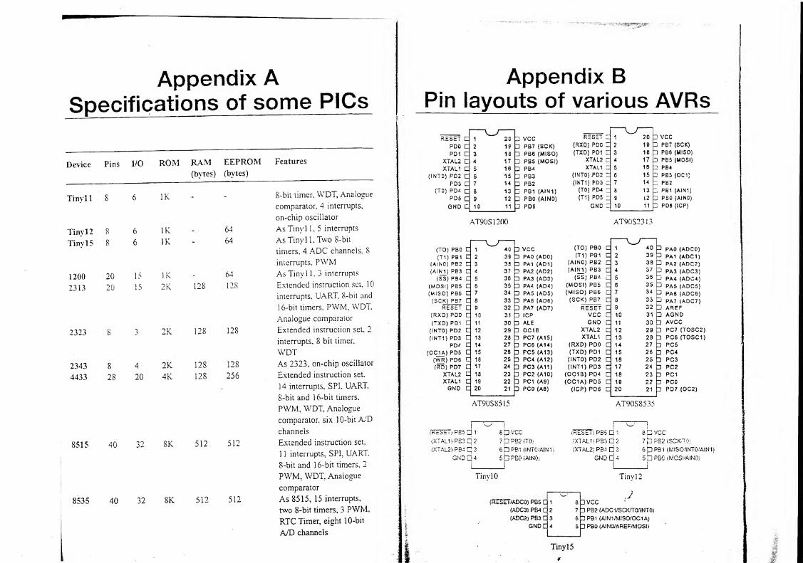
Appendix ASpecifications of some PICs
Device Pins I/O ROM RAM(bytes)
EEPROM(bytes)
Features
Tinyl
1
8 6 IK - 8-bit timer, WDT, Analogue
comparator, 4 interrupts,
on-chip oscillator
Tiny12 8 6 IK - 64 As Tinyl 1, 5 interrupts
TinylS 8 6 IK 64 As Tinyl 1, Two 8-bit
timers, 4 ADC channels. 8
interrupts. PWM
1200 20 15 IK - 64 As Tinyl 1. 3 interrupts
2313 20 15 2K 128 128 Extended instruction set, 1
0
interrupts, UART. 8-bit and
16-bit timers, PWM, WDT.
Analogue comparator
2323 8 3 2K 128 128 Extended instruction set. 2
interrupts, 8 bit timer.
WDT2343 8 4 2K 128 128 As 2323, on-chip oscillator
4433 28 20 4K 128 256 Extended instruction set.
14 interrupts, SPI, UART.
8-bit and 16-bit timers,
PWM, WDT, Analogue
comparator, six 1 0-bit AT)
channels
8515 40 32 8K 512 512 Extended instruction set,
1 1 interrupts, SPI, UART.
8-bit and 1 6-bit timers, 2
PWM, WDT, Analogue
comparator
8535 40 32 8K 512 512 As 8515, 15 interrupts,
two 8-bit timers, 3 PWM,
RTC Timer, eight 10-bit
A/D channels
Appendix BPin layouts of various AVRs
RESET C 1 20 VCC RESET E 1 20
pdo c 2 IP PB7 (SCK) (RXD) PDO E 2 19
PD1 C 3 18 3 PB6 (MISO) (TXD) PD1 E 3 18
XTAL2 E 4 17 3 PB5 (MOSI) XTAL2 E 4 17
XTAL1 C 5 16 PB4 XTAL1 E 5 16
(INTO) PD2 C 6 15 PB3 (INTO) PD2 E 6 15
PD3 E 7 14 PB2 (INTI) PD3 E 7 14
(TO) PD4 C 8 13 3 PB1 (AIN1) (TO) PD4 r 8 13
PD5 E 9 12 PBO (AINO) (T1) PD5 Z 9 12
GND C 10 11 3 PD6 GND E 10 11
(TO) PBO(T 1 )
PB1(AINC) PB2(AIN1) PB3
(SS) P94
(MOS!) PBS(MISO) PB6(SC K) PB7
RESET(RXD) PDO
(TXD) PD1(INTO) PD2(INTI) PD3
PD'(OC1A) PD5(WR) PD6(RD) PD7
XTAL2XTAL1GND
AT90S1200 AT90S2313
i 40 3 VCC (TO) PBO E "l 40
2 39 PAO (ADO) (T1 ) PB1 E 2 39
3 38 3 PA1 (ADI) (AINO) PB2 C 3 38
4 37 PA2 (AD2) (AIN1) PB3 C 4 37
5 38 =3 PA3 (AD3) (SS) PB4 E 5 36
6 35 3 PA4 (AD4) (MOSI) PB5 E 6 35
7 34 3 PA5 (AD5) (MISO) PB6 C 7 34
8 33 3 PAS (AD6) (SCK) PB7 C 8 33
9 32 PA7 (AD7) RESET E 9 32
10 31 ICP VCC E 10 31
11 30 3 ALE GND C 11 30
12 29 3 OC1B XTAL2 C 12 29
13 28 3 PC7 (A15) XTAL1 E 13 28
14 27 3 PC6 (A14) (RXD) PDO C 14 27
15 26 FC5 (A13) (TXD) PD1 E 15 26
16 25 3 PC4 (A12) (INTO) PD2 E 18 2517 24 3 PC3 (All) (INTI) PD3 E 17 24
18 23 PC2 (AIO) (OC1B) PD4 E 18 2319 22 3 PCI (A9) (OC1 A) PD5 E 18 2220 21 3 PCO (AS) (ICP) PD6 E 20 21
] VCC] PB7 (SCK)
] PB8 (MISO)
} PB5 (MOSI)
} PB4
i PB3 (OC1)
3 PB2
; PB1 (AIN1)
3 PBO (AINO)
j PD6 (ICP)
PAO (ADCO)PA1 (ADC 1
)
PA2 (ADC2)
PA3 (ADC3)PA4 (ADC4)
PAS (ADC5)PA6 (ADC6)PA 7 (ADC7)AREFAGNDAVCCPC7 (TOSC2)
PC6 (TOSC1
)
PC5PC4PC3PC2PCIPCOPD7 (OC2)
AT90S8515 AT90S8535
{KcSiiT} P55 d 3
(XTAL1)PB3C}2
(XTAL2) PB4 q 3
GND Q 4
8 p VCC
7 P PB2 .TO)
5 p PBl (INTO/AIN 1)
5 p PBO i AINO)
h PB5 q 1
(X7AL1) PB3 C 2
(XTAL2) PB4 2
GND Q 4
8 p VCC7pPS2 (SCK-TO;
6p PB1 (MIS0.1NTO/AW1)
5b PBO (MOSI-AINO)
(RE5E7/ADCO) PB5 E i
(ADC3) PB4C 2
(ADC2) PB3C 3
GND d 4
8DVCC7h PB2 (ADCI/SCK.'TOl'INTO)
6 3P81 (AIN1/MISO/OC1A)
5 3 PBO (AINO/AREF/MOSI)
TinylS
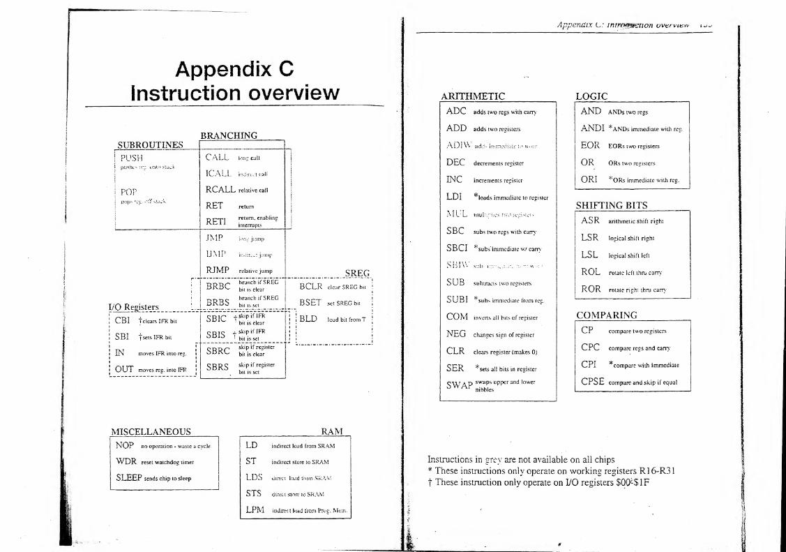
Appendix CInstruction overview
SUBROUTINES
pusin> mg. s
BRANCHING
CALL lor; LI CUli
1CALL indirect calf
RCALL relative call
RET return
T?PTT return, enabling* * interrupts
JMP jump
UMP
l.Vn: jump
indirect jump
170 Registers
i CBI T clears IFR bit
! SBI J sets IFR bit
: in moves IFR into reg.
> OUT moves res. into IFR
RJMP relative jump
t» branch if SREGBRBC
BRBS
bit is clear
branch if SREGbit is set
SB1C ts
Kk,pif
,
1FR
bit is clear
od to j. skip if IFR
^l^^bitjssetnppp skip ifregisterODKU
bit is clear
SBRS s*ip register
bit is set
SREGBCLR clear SREG bii
BSET set SREG bit
BLD load bit from T
MISCELLANEOUS
NOP no operation - waste a cycle
WDR reset watchdog timer
SLEEP sends chip to sleep
LD indirect load from SRAM
ST indirect store to SRAM
LOS direct load from .SRAM
STS direct store to SRAM
LPM indirect load from Frog. Mem.
Appendix C: mrrrmmenon overview
ARITHMETIC LOGIC
ADC adds tw'o regs with cam AND ANDs two regs
ADD adds two registers ANDI *ANDs immediate with reg.
AD i YV arid' immediate to u v=rd EOR EORs two registers
DEC decrements register OR ORs two registers
INC increments register OR1 *ORs immediate w'ith reg.
LDI *loads immediate to register
SHIFTING BITSAIL L mui: \ptcs two ;vg- ^
SBC subs two regs w'ith cam
SBCI *subs' immediate w/ carry
SBIW s.il)
SUB subtracts two registers
SUB I *subs immediate from reg.
COM inverts all bits of register
NEG changes sign of register
CLR clears register (makes 0)
SER *seis all bits in register
QW A P swaPs upper and lowerp w Ar
nibbles
ASR arithmetic shift right
LSR logical shift right
LSL logical shift left
ROL rotate left thru carry
ROR rotate right thru cam
COMPARINGCP compare two registers
CPC compare regs and cany’
CPI *compare with immediate
CPSE compare and skip if equal
Instructions in grey are not available on all chips
* These instructions only operate on working registers R1 6-R3
1
t These instruction only operate on I/O registers $Q0-$1F
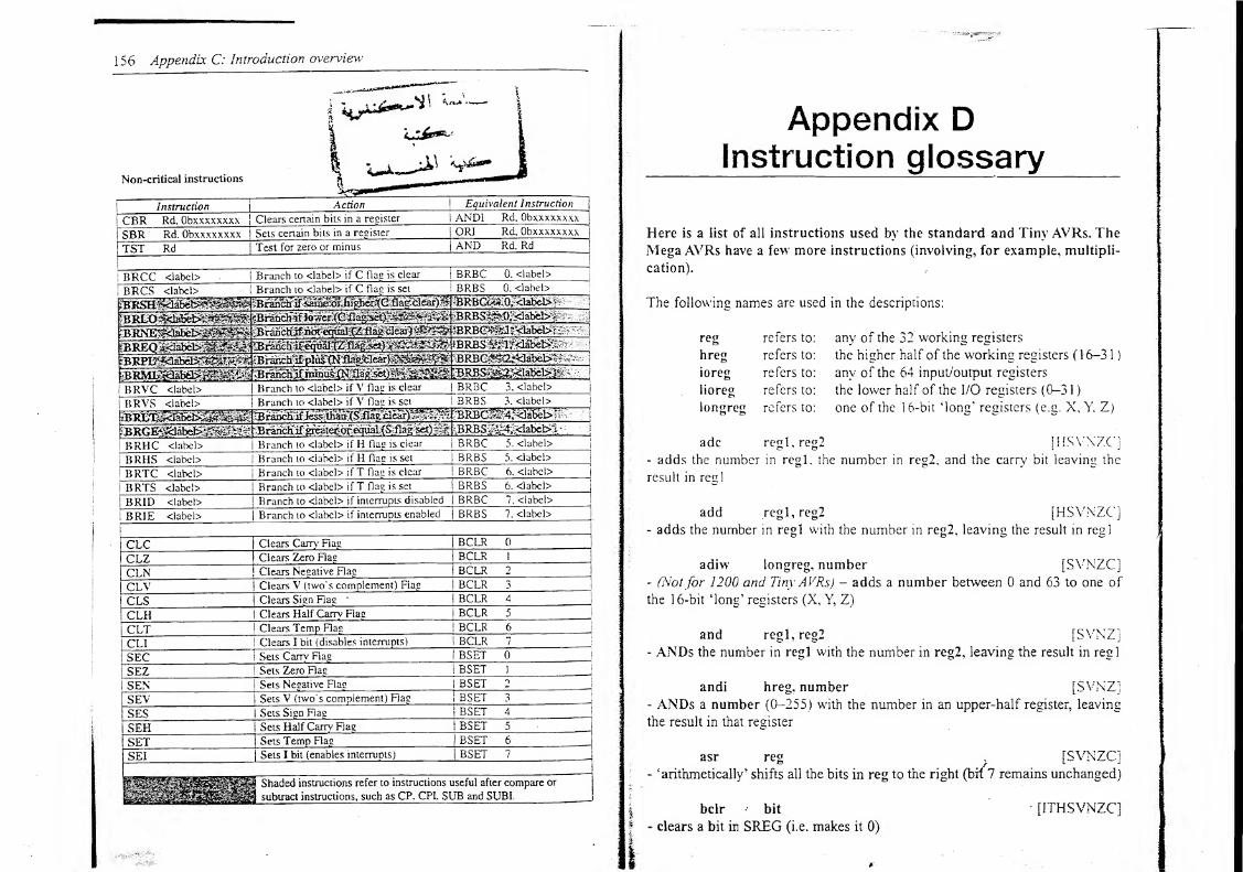
156 Appendix C: Introduction overview
Non-critical instructions
Instruction
CBR Rd, Obxxxxxxxx
SBR Rd. Obxxxxxxxx
TST Rd
BRCC <Iabd>~~
BRCS <labei>
Action
Clears cenain bits in a register
Sets certain bits in a register
Test for zero or minus
BREOlpa&ebf
1 Branch to <label> if C flag is clear
I Branch to <label> if C flag is set
mmm
Equivalent Instruction
ANDI Rd. Obxxxxxxxx
ORI Rd, Obxxxxxxxx
AND Rd. Rd
j BRBC 0. <label>
jBRBS 0. <label>
IBrasch®SSE^S^ggiljSi
j
BRVC <label>
|BRVS <label>
BRHC <label>
BRHS <label>
BRTC <label>
BRTS <labe!>
BRID <label>
BRIE <label>
Branch to <label> if V flag is clear
Branch to <label> if V flag is set
fH
jBranch to <label> if H flag is clear
Branch to <iabel> if H flag is set
Branch to <label> if T flag is clear
Branch to <label> if T flag is set
Branch to <label> if interrupts disabled
Branch to <label> if interrupts enabled
Clears Carry Flag
Clears Zero Flag
Clears Negative Flag
Clears V (two's complement) Flag
Clears Sign Flag•
{ Clears Half Canrv Flag
Clears Temp Flag
Clears I bit (disables interrupts)
Sets Carry Flag
Sets Zero Flag
Sets Negative Flag
Sets V (two's complement) Fag
Sets Sign Flag
Sets Half Carry Fag
Sets Temp Fag
Sets I bit (enables interrupts)
BRBG^2^3abe^mmm
BRBC 3. <labcl>" BRBS 3. <label>
BRBC 5. <label>
BRBS 5. <labcl>
BRBC 6. <label>
BRBS 6. <label>
BRBC 7. <label>
1BRBS 7. <label>
BCLR 0
BCLR 1
BCLR 2
BCLR 3~ BCLR 4
BCLR 5
BCLR 6
j BCLR 7
1 BSET 0
1BSET 1
j BSET 2
BSET 3
BSET 4
BSET 5
BSET 6
BSET 7
Shaded instructions refer to instructions useful after compare or
subtract instructions, such as CP. CPL SUB and SUBI.
Appendix Dinstruction glossary
Here is a list of all instructions used by the standard and Tiny AVRs. TheMega AVRs have a few more instructions (involving, for example, multipli-
cation).
The following names are used in the descriptions:
reg refers to: any of the 32 working registers
hreg refers to: the higher half of the working registers (16-3 1
)
ioreg refers to: any of the 64 input/output registers
lioreg refers to: the lower half of the I/O registers (0-31
)
longreg refers to: one of the 16-bit ‘long’ registers (e.g. X, Y. Z)
adc regl,reg2 [USYNZCj- adds the number in regl. the number in reg2, and the carry bit leaving the
result in regl
add regl, reg2 [HSVNZC]- adds the number in regl with the number in reg2, leaving the result in regl
adiw longreg, number [SVNZC]- (Not for 1200 and Tiny AVRs) - adds a number between 0 and 63 to one of
the 16-bit ‘long’ registers (X, Y, Z)
and regl,reg2 [SVNZ]- ANDs the number in regl with the number in reg2, leaving the result in regl
andi hreg, number [SVNZ]- ANDs a number (0—255) with the number in an upper-half register, leaving
the result in that register
asr reg}
[SVNZC]- ‘arithmetically’ shifts all the bits in reg to the right (bit 7 remains unchanged)
bclr bit
- dears a bit in SREG (i.e. makes it 0)
¥
[ITHSVNZC]
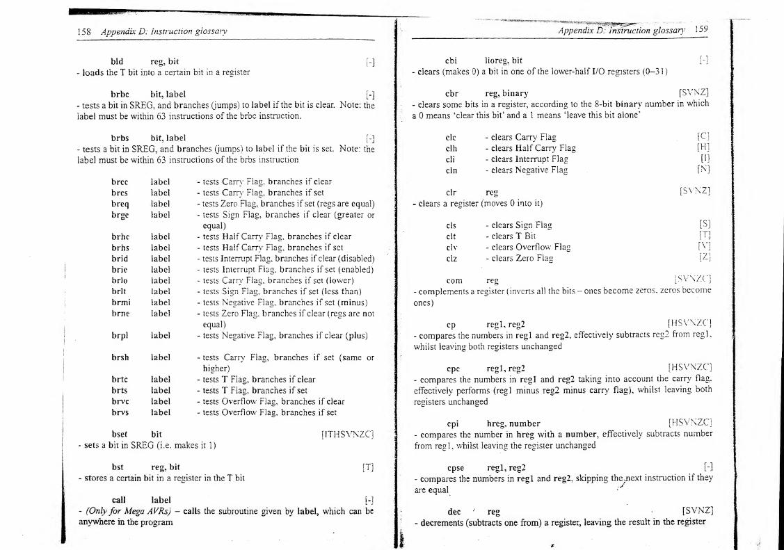
158 Appendix D: Instruction glossary
bid reg, bit [-]
- loads the T bit into a certain bit in a register
brbc bit, label [-]
- tests a bit in SREG, and branches (jumps) to label if the bit is clear. Note: the
label must be within 63 instructions of the brbc instruction.
brbs bit, label [-]
- tests a bit in SREG, and branches (jumps) to label if the bit is set. Note: the
label must be within 63 instructions of the brbs instruction
brcc label - tests Carry Flag, branches if clear
brcs label - tests Carry Flag, branches if set
breq label - tests Zero Flag, branches if set (regs are equal)
brge label - tests Sign Flag, branches if clear (greater or
equal)
brhc label - tests Half Carry Flag, branches if clear
brhs label - tests Half Carry Flag, branches if set
brid label - tests Interrupt Flag, branches if clear (disabled)
brie label - tests Interrupt Flag, branches if set (enabled)
brio label - tests Carry Flag, branches if set (lower)
brit label - tests Sign Flag, branches if set (less than)
brmi label - tests Negative Flag, branches if set (minus)
brne label - tests Zero Flag, branches if clear (regs are not
equal)
brpl label - tests Negative Flag, branches if clear (plus)
brsh label -tests Carry Flag, branches if set (same or
higher)
brtc label - tests T Flag, branches if clear
brts label - tests T Flag, branches if set
brvc label - tests Overflow Flag, branches if clear
brvs label - tests Overflow Flag, branches if set
bset bit [ITHSVNZC]- sets a bit in SREG (i.e, makes it 1)
bst reg, bit [T]
- stores a certain bit in a register in the T bit
call label [-]
- (Only for Mega AVRs) - calls the subroutine given by label, which can be
anywhere in the program
Appendix D: Instruction glossary: 1 3y
cbi lioreg, bit [-]
- clears (makes 0) a bit in one of the lower-half I/O registers (0-31
)
reg, binary [SVNZ]
- clears some bits in a register, according to the 8-bit binary number in which
a 0 means 'clear this bit5
and a 1 means ieave this bit alone5
clc - clears Cam7 Flag [C]
clh - clears Half Carry Flag [H]
cii - clears Interrupt Flag [1]
cln - clears Negative Flag [N]
clr reg [SVNZ]
- clears a register (moves 0 into it)
els - clears Sign Flag [S]
clt - clears T Bit [T]
civ - clears Overflow Flag [V]
elz - clears Zero Flag [Z]
com reg [SYNXC'j
- complements a register (inverts all the bits - ones become zeros, zeros become
ones)
cp regl, reg2 [HSVNZC]- compares the numbers in regl and reg2, effectively subtracts reg2 from regl,
whilst leaving both registers unchanged
cpc regl,reg2 [HSVNZC]- compares the numbers in regl and reg2 taking into account the carry flag,
effectively performs (regl minus reg2 minus carry flag), whilst leaving both
registers unchanged
cpi hreg, number [HSVNZC]- compares the number in hreg with a number, effectively subtracts number
from real, whilst leaving the register unchanged
cpse regl, reg2 H- compares the numbers in regl and reg2, skipping the .next instruction if they
are equal
dec - reg [SVNZ]
- decrements (subtracts one from) a register, leaving the result in the register
1 60 Appendix D: Instruction glossary
eor regl, reg2 [SVNZ]- exclusive ORs the number in regl with the number in reg2, leaving the result
in regl
icall [-]
- (Not for 1200 and Tiny AVRs) - (indirectly) calls a subroutine with address
given by Z
ijmp [-]
- (Not for 1200 and Tiny AVRs) - (indirectly) jumps to the address given by Z
in reg, ioreg [-]
- copies the number in an I/O register into a working register
inc reg [SYNZ]- increments (adds one to) a register, leaving the result in the register
jmp label [-]
- (Only for Mega AVRs) - jumps to the section called by label, which can be
anywhere in the program
id reg, longreg H- loads the memory location pointed to by longreg into a register (reg)
Id reg, Iongreg+ [-]
- (Not for 1200 and Tiny AVRs) - loads the memory* location pointed to by
longreg into reg, and then adds one to longreg
Id reg, -longreg [-]
- (Not for 1200 and Tiny AVRs) - subtracts one from longreg. and then loads
the memory location pointed to by longreg into reg
ldd reg, longreg-fnumber [-]
- (Not for 1200 and Tiny AVRs) - loads the memory location pointed to by the
Y or Z registers into reg, and then adds a number (0-63) to longreg (Note:
doesn *t work with X)
Idi hreg, number [-]
- loads a number (0-255) into an upper-half register (16-31)
Ids reg, number [-]
- (Not for 1200 and Tiny AVRs) - loads the contents of memory at address
(number) registers into reg, where number can be between 0 and 65 535 (i.e. up
to 64K)
Appendix D: Instruction glossary 1 6
1
lpm [-]
- (Not for 1200) - loads into R0 the contents of the program memory at the
address specified by the Z register
lsl reg [SVNZC]- ‘logically’ shifts all the bits in reg to the left (bit 7 goes into Carry' flag, bit 0
is 0)
lsr reg [SVNZC]- ‘logically’ shifts all the bits in reg to the right (bit 0 goes into Carry flag, bit
7 is 0)
mov regl, reg2 {-]
- copies (moves) the number in reg2 into regl
neg reg [H SVNZC]- makes the number in a register negative (20 becomes -20, equivalent to 236)
nop [-]
- this stands for no operation, literally ‘do nothing' - good for wasting a clock
cycle
or regl,reg2 [SVNZ]- inclusive ORs the number in regl with the number in reg2, leaving the result
in reg 1
ori hreg, number [SVNZ]- inclusive ORs a number (0-255) with the number in an upper-half register,
leaving the result in that register
out ioreg, reg [-]
- copies the number in a working register out to an I/O register
pop reg [-]
- (Notfor 1200 and Tiny AVRs) - pops the top of the stack into a register
push reg [-]
- (Notfor 1200 and TinyAVRs) - pushes the contents of a register onto the stack
rcall label [-]
- calls the subroutine labeled by label, which must be not further than 2048
instructions from the ijmp instructions (i.e. a relative call)
162 Appendix D: Instruction glossary
ret [-]
- returns from a subroutine (executes the line after the original call instruction)
reti [{]
- returns from a subroutine, and sets the interrupt flag
rjmp label [-]
- jumps to a part of the program labeled by label, which must be not further
than 2048 instructions from the ijmp instructions (i.e a relative jump).
rol reg [SVNZC]- rotates all the bits in reg to the left (C flag goes into bit 0, bit 7 goes into CFlag)
ror reg [SVNZC]- rotates all the bits in reg to the right (C flag goes into bit 7, bit 0 goes into Cflag)
sbc regl,reg2 [HSVNZC]- subtracts the number in reg2 and the carry bit from regl . leaving the result
in regl
sbci hreg, number [HSVNZC]- subtracts a number (0-255) and the carry bit from the number in an upper-
half register, leaving the result in that register
sbi lioreg, bit [-]
- sets (makes 1) a bit in one of the lower-half I/O registers (0-31)
sbic lioreg, bit [-]
- tests a bit in a lower-half I/O register (0-31), and skips the next instruction if
is clear
sbis lioreg, bit [-]
- tests a bit in a lower-half I/O register (0-31 ), and skips the next instruction if
is set
sbiw longreg, number [SVNZC]- (Not for 1200 and Tiny AVRs) - subtracts a number between 0 and 63 from
one of the 16-bit ‘long’ registers (X, Y, Z)
sbr reg, binary [SVNZ]- sets some bits in a register, according to the 8-bit binary number in which a
1 means ‘set this bit’ and a 0 means ‘leave this bit alone’
Appendix D: Instruction glossaiy 1 63
[-]sbrc reg, bit
- tests a bit in a register, and skips the next instruction if is clear
reg, bit
tests a bit in a register, and skips the next instruction if is set
sec - sets Carry Flag [C]
seh - sets Half Carry Flag [H]
sei - sets Interrupt Flag [I]
sen - sets Negative Flag [N]
ser reg [-]
register (moves 255 / SFF / Obi 1 1 1 1 1 1 1 into it)
ses - sets Sign Flag [S]
set - sets T Bit [T]
sev - sets Overflow' Flag [V]
sez - sets Zero Flag [Z]
sleep [-]
- sends the chip to sleep, a low-power mode (woken up through reset or interrupt)
st reg, longreg H- stores the number in a register (reg) to the memory location pointed to by
longreg
st reg, longreg* H- (Not for 1200 and Tiny AVRs) - stores the number in reg to the memory loca-
tion pointed to by longreg, and then adds one to longreg
st reg, -longreg H- (Not for 1200 and Tiny AVRs) - subtracts one from longreg, and then stores
the number that’s in reg to the memory location pointed to by longreg
std reg, longreg+number H- (Notfor 1200 and Tiny AVRs) - stores the number in reg to the memory loca-
tion pointed to by the Y or Z registers, and then adds a number (0-63) to
longreg (Note: doesn *t work with X)
sts reg, number / H- (Not for 1200 and Tiny AVRs) - stores the number in reg at memory address
(number), where number can be between 0 and 65535 (i.e. up to 64K)
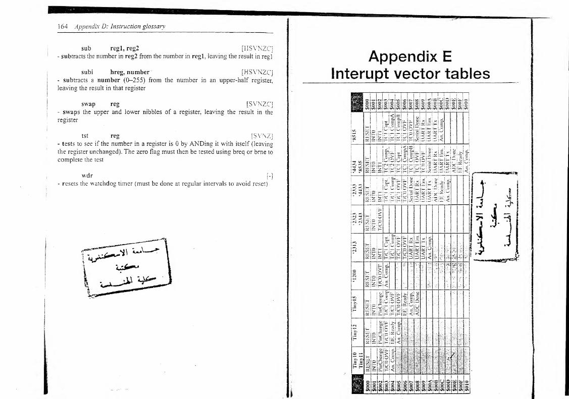
1 64 Appendix D: Instruction glossary
|
sub regl, reg2 [HSVNZC]- subtracts the number in regl from the number in regl, leaving the result in regl
subi hreg, number [HSVNZC]- subtracts a number (0-255) from the number in an upper-half register,
leaving the result in that register
swap reg [SVNZC]- swaps the upper and lower nibbles of a register, leaving the result in the
registeri
l
tst reg [SVNZ]- tests to see if the number in a register is 0 by ANDing it with itself (leaving
the register unchanged). The zero flag must then be tested using breq or brne to
complete the test
!
wdr [-]
- resets the watchdog timer (must be done at regular intervals to avoid reset)
i
200
‘2313
‘2323
‘2333
‘4434
‘8515
Appendix EInterupt vector tables
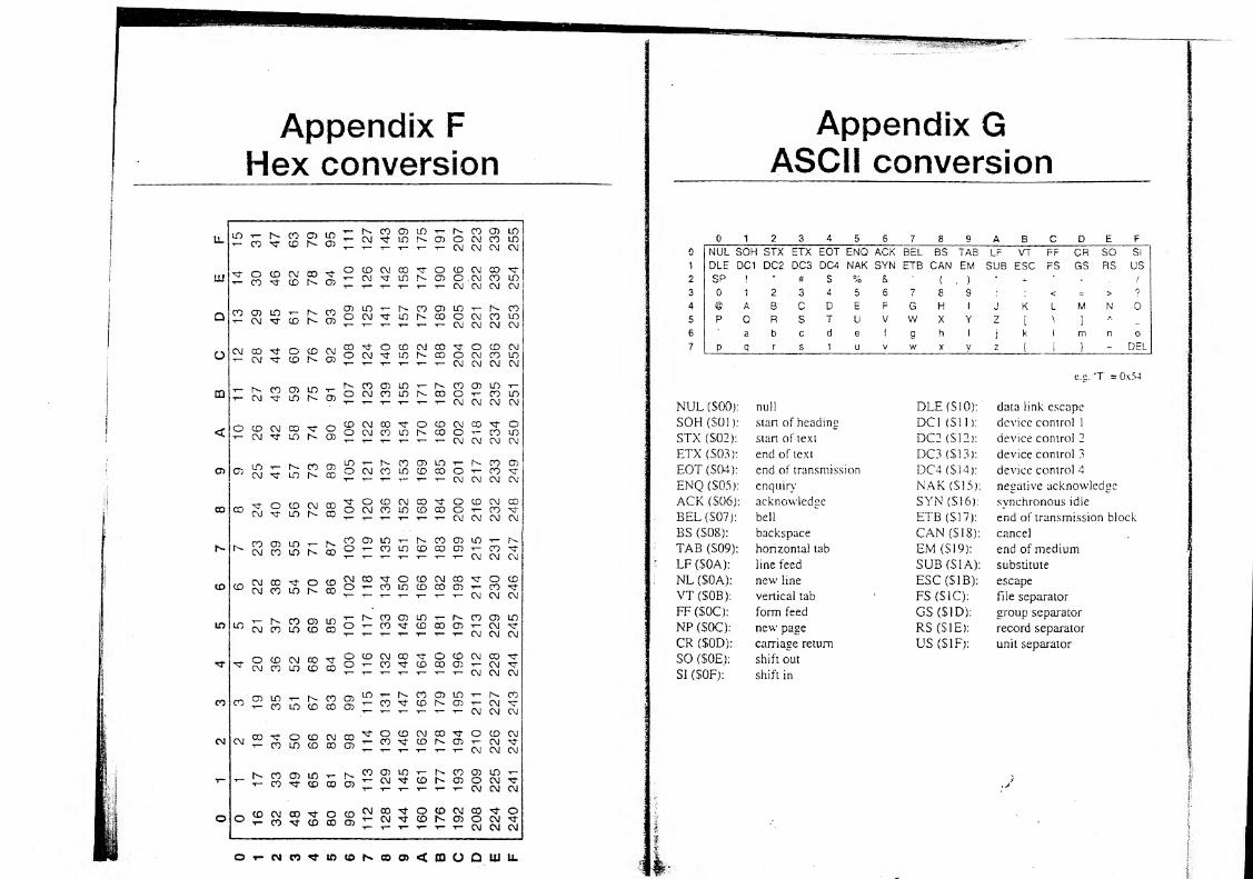
Appendix F
Hex conversion
Appendix GASCII conversion
lo r- n co O) inr- n ^ to n O)
NCOG>U)r-NCOCDLOCM^iONOOWCOin-r-r-f-’r-'r-CMCMCMCM
^ ^ ° ? 0 N S ^ W ^ 10 N 05 ^ ^ ^ ^CM C\J (M C\J
CM ^ CD N O)
o)in^Ncoo)tr)r-scoOCM-^LONCOOCMCOUOT-T-f-«r-*«-T-CMCMCMCM
rv tn ^ o cn fv 23 ^ ° ^ ^ 03 ^ ° 0 w
N CO O) ID rCM ^ LO N CD
NCOO)LOi-N0O)ir)T-OCMCOLONCOO-r-COLOT— 1— T T— 1 CM CXI C\J C\J
<2wSSN§ OWCOlONCOOT* Wir)T-c\]^ior-.G),r_^,r_,r_ T_,r
_ CNJCsJCg CNJ
CM ^ U) N CO
"v C 0 CM COCM M- ID N O
IDt-NCOO)IO^NCOCDOCMCOLOCDCOOi-CD^f“T*T- T”r'i-(MCMCMCM
^OOCMCO^OCDCMCOO CM CO LO 0 CD O04 OJ CM CM
rtflVinr- N WO)WirNW ®lOT.N
(Mffi^OfflWCO^O0CM0^O0
10 10 S S S £ o ^ £ $ <e ® 2 w cm. S
,O0CM0^OCOCM 2? OCOCM SJcm co in co co CO^00O)r-CM^
t-t-t-t-t-CMCMCM
0 1 2 3 4 5 6 7 8 9 A B C D E F
NUL SOH STX ETX EOT ENQ ACK BEL BS TAB LF VT FF CR SO SI
DIE DC1 DC2 DC3 DC4 NAK SYN ETB CAN EM SUB ESC FS GS RS USSP 1
-# $ % &
*
( )
*+ - /
0 1 2 3 4 5 6 7 8 9J
< = > ?
@ A B C D E F G H 1 J K L M N 0P Q R S T U V W X Y 2
[\
]
A
a b c d e f g h !i
k 1 m n 0
P q r s t u V w X y 2 { 1 }- DEL
c.c. ‘T = 0x54
NUL ($00): null DLE ($10): data link escape
SOH (SOI): start of heading DO ($11): device control 1
STX ($02): stan of text DC2 ($12): device control 2
ETX ($03): end of text DC3 ($13): device control 3
EOT ($04): end of transmission DC4 ($14): device control 4
ENQ ($05): enquiry NAK ($15): negative acknowledge
ACK ($06): acknowledge SYN ($16): synchronous idle
BEL ($07): bell ETB ($17): end of transmission block
BS ($08): backspace CAN ($18): cancel
TAB (S09): horizontal tab EM ($19): end of mediumLF ($0A): line feed SUB ($1 A): substitute
NL ($0A): new line ESC (S 1 B): escape
VT (SOB): vertical tab FS (SIC): file separator
FF ($0C): form feed GS (SID): group separator
NP (S0C): new page RS (SIB): record separator
CR (SOD): carriage return US($1F): unit separator
SO ($0E): shift out
SI (S0F): shift in
O) 0 T- N 0 O)-T- CO in CD CO CD
LOt-NCOO0r-SCOi-OOXf^NCDT-CMVr-rr-r-rr-WCMCM
ro^o0CM0^2!2!!!PS o S2!
N CO O) 0 r- Nt- CO Tf CD CO O)
O) LO **— N CO 03 in T-CMM’CONOJOCM^r* r- t- t- i- CM CM W
^0Wm^O0CM©tOOCM©^Ooo2co®S§S^ w ^cdno)Ow^
O r W (0 ID (0 N CO O) < OO Q UI u.
Appendix HWhen all else fails, read this
You should find that there are certain mistakes which you make time and time
again (I do!). I’ve listed some popular ones here :
? Have you put a colon after your labels, i.e. start: and not start?
? Have you tried to use sbi. cbi, sbis or sbic with I/O registers S20-S3F9
? Are you remembering to reset counting registers?
? Have you set registers to correct initial values in Init?
? Have you remembered that on Tiny 10 and Tiny] 1. PB5 is input only?
? Have you set up the stack pointer (SPL/SPH) if necessary?
? Are you writing/reading 2-bvte registers such as TCNT1H,L in the
correct order?
? If you are having a total nightmare and NOTHING is working . . . have you
specified the correct AVR at the top?
Appendix I
Contacts and further reading
John Morton: [email protected]
ATMEL website: http://www.atmel.com
Kuhnel, Claus (1998) AVR RISC Microcontroller Handbook, Newnes
(gives more details of the inner architecture ofAVRs)
Brimicombe, MAY. (1985) Electronic Systems ,Nelson
(great text for general electronics)
Some fun AVR projects: http://www.riccibitti.com/designs.htm
Random numbers: http://www.physics.carleton.ca/courses/75.502/slides/
monte 12
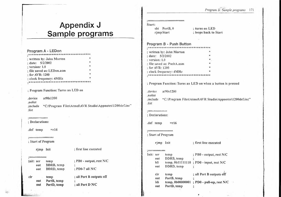
Appendix J
Sample programs
Program A - LEDon.*************************************9
;written by: John Morton *
;date: 5/2/2002
*
;version: 1.0
*
;file saved as: LEDon.asm *
;for AYR: 1200
;clock frequency: 4MHz *
**************************************
;Program Function: Turns an LED on
.device at90sl200
.nolist
.include “C:\Program Files\Atmel\AVR StudioVAppnotes\1200def.inc”
.list
;Declarations:
.def temp =rl6
;Start of Program
rjmp Init
Init: ser temp
out DDRB, temp
out DDRD, temp
clr temp
out PortB, tempout PortD, temp
: First line executed
; PB0 - output, rest N/C
; PD0-7 all N/C
; all Port B outputs off
•all Port D N/C
Program B: Sample programs 1 7
1
; turns on LED; loops back to Start
Program B - Push Button. *************************************9
;written by: John Morton *
; date: 5/2/2002 *
; version: 1.0
;file saved as: PushA.asm *
: for AYR: 1200 *
; clock frequency: 4MHz *
. *************************************9
; Program Function: Turns an LED on when a button is pressed
.device at90sl200
.nolist
.include uC:\Program Files\AtmeI\AYR Studio\Appnotes\1200def.inc’,
.list
; Declarations:
.def temp =rl6
; Start of Program
rjmp Init;first line executed
9
Init: ser temp;PB0 - output, rest N/C
out DDRB, temp9
Idi temp, OblllllllO : PD0 - input, rest N/Cout DDRD, temp
9
clr temp;all Port B outputs off
out PortB, temp 9
ldi temp, ObOOOOOOOl ; PD0 - pull-up, rest N/Cout PortD, temp 9
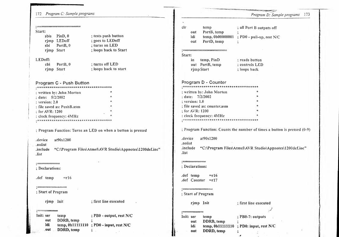
1 72 Program C: Sample programs
Start:
sbis PinD, 0
rjmp LEDoffsbi PortB, 0
rjmp Start
I
LEDoff:
cbi PortB, 0
rjmp Start
; tests push button
;goes to LEDoff
; turns on LED;loops back to Start
; turns off LED;loops back to start
Program C - Push Button.*************************************
;written by: John Morton *
; date: 5/2/2002 *
;version: 2.0
*
; file saved as: PushB.asm *
; for AVR: 1200
; clock frequency: 4MHz *
.*************************************
; Program Function: Turns an LED on when, a button is pressed
.device at90sl200
.nolist
.include “C:\Program Files\Atmel\AVR Studio\Appnotes\1200def.inc”
.list
; Declarations:
.def temp -rl6
; Start of Program
rjmp Init ; first line executed
lnit: ser temp ; PBO - output, rest N/Cout DDRB, temp
;
Idi temp, OblllllllO ; PDO - input, rest N/Cout v DDRD, temp ;
Program D: Sample programs 173
clr temp; all Port B outputs off
out PortB, temp;
Idi temp, ObOOOOOOOl ; PDO - pull-up, rest N/Cout PortD, temp
;
Start:
in temp, PinD
out PortB, temp
rjmp Start
; reads button
; controls LED; loops back
Program D - Counter.*************************************
; written bv: John Morton *
: date: 7/2/2002
; version: 1.0 *
; file saved as: counter.asm *
; for AVR: 1200
: clock frequency: 4MHz *
.*****•*•**********•*•***** Sr 'k'k-k'k-k-k'k-k-k'k-k
; Program Function: Counts the number of times a button is pressed (0-9)
.device at90sl200
.nolist
.include “C:\Program Files\Atmel\AVR Studio\Appnotes\1200def.inc”
.list
;Declarations:
.def temp =rl6
.def Counter =r!7
iStart of Program
rjmp Init; first line executed
Init: ser temp;PB0-7: outputs
out DDRB, temp;
Idi temp, OblllllllO ; PDO: input, rest N/Cout DDRD, temp ;
~
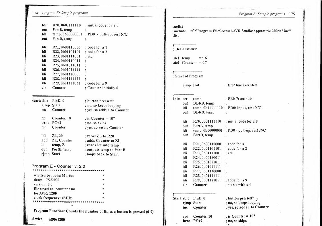
1 74 Program E: Sample programs Program E: Sample programs 1 75
.nolist
.include “C:\Program FiIes\AtmeI\AVR Studio\Appnotes\1200def.inc”
.list
;Declarations:
.def temp =r!6
.def Counter =r!7
;Start of Program
rjmp Init ;First line executed
}
Init: ser temp ;PBO-7: outputs
out DDRB, temp
ldi temp. Obi 1111110 ;PD0: input, rest N7C
out DDRD, temp
ldi R20, ObOl 111110 ; initial code for a 0
out PortB, temp
ldi temp, ObOOOOOOOl ;PD0 - pull-up, rest N/C
out PortD, temp
ldi R21,0b001 10000 ; code for a 1
ldi R22, ObOl 101 101 ;code for a 2
ldi R23, ObOll 11001;etc.
ldi R24, ObOOl 10011 5
ldi R25, ObOl 01 1011 9
ldi R26, ObOl 01 1 111 5
ldi R27, ObOlllOOOO y
ldi R28, ObOllll 111 *
ldi R29, ObOll 11011 ; code for a 9
clr Counter ; starts with a 0
5
Startrsbic PinD, 0 ;button pressed? j
rjmp Start ; no, so keeps looping
inc Counter ;yes, so adds 1 to Counter
cpi Counter, 10 ; is Counter - 10?
brne PC+2 ; no, so skips
1 76 Program F: Sample programs
clr Counter
ldi ZL, 20
add ZL, Counter
Id temp, Zout PortB, temp
ReieaseWait:
sbis PinD, 0
rjmp ReieaseWait
rjmp Start
;yes, so resets Counter
; zeros ZL to R20
;adds digit to ZL
;reads Rx into temp
;outputs temp to Port B
;button released?
; no, so keeps looping
;yes, so loops back to start
Program F - Chaser,'k'k’k'k'k-k-k'k'k'k'k-k-k-k-k’k'k'k‘k it'k’k-k-k‘k'k-)ck -tc*** * it ic Jc *
; written by: John Morton *
; date: 7/2/2002
: version: L0 *
: file saved as: chaser.asm *
; for AYR: 1200 *
: clock frequency: 2.4576MHz *
**"*"*•*"*•* •k'k*'k*±ifick1:'k-k *••***•* •*"**:&* *******
i
i
Program F. Sample programs 1 77
out DDRB, temp ;
ldi temp, ObllllllOO ;PD0, 1 - input, rest N1C
out DDRB, temp ;
ldi temp, ObOOOOOOOl ; initially just PB0 on
out PortB, temp ;
ldi temp, ObOOOOOOll ; PD0, 1 - pull-ups, rest N/C
out PortD, temp ;
ldi temp, ObOOOOOlOl ; sets up timer to count at CK/1024
out TCCR0, temp ;
ldi Mark240, 240
ldi Counter, 5 ;
ldi Speed, 5 ;
; checks down button
; not pressed, jumps
; slows down time
: has Speed reached 11?
;jumps to ReleaseDown if not equal
; subtracts one from Speed
; waits for down button to be released
UpTest:
sbic
rjmp
dec
brne
inc
ReleaseUp
sbis
rjmp
Timer:
in temp, TCNT0 ; reads Timer 0 into temp
cp temp, Mark240 ; compares temp with Mark240
brne Timer ;if not equal loops back to Timer
subi Mark240, -240 ;adds 240 to Mark240
dec Counter ; subtracts one from Counter
brne Start ; if not zero loops back to Start
PinD, 1 ;checks up button
Timer ; not pressed, jumps
Speed ; speeds up time
ReleaseUp ;jumps to Timer if not 0
Speed ; adds one to Speed
PinD, 0 ; waits for up button to be released
ReleaseUp ;
Start: sbic PinD, 0
rjmp UpTest
inc Speed
cpi Speed, 11
brne ReleaseDown
dec Speed
ReleaseDown:
sbis PinD, 0
rjmp ReleaseDown
1 78 Program G: Sample programs
;set time has passed, rotates LEDs
mov Counter, Speed ;resets Counter
in temp, PortB ; reads in current state
lsi temp ;rotates to the left
brcc PC+2 ;checks Carry Flag, skip if clear
ldi temp, ObOOOOOOOl;resets to PB0 on, others off
out PortB, temp ; outputs to PortB
rjmp Start ; loops back to Start
Program G - Counter v. 3.0.**************If**********************
;written by: John Morton *
;date: 9/2/2002
;version: 3.0
*
; file saved as: counter.asm *
; for AVR: 1200 *
; clock frequency: 4MHz *
.*************************************
Program G: Sample programs 1 79
Debounce:
ldi Delayl, 0x80;sets up counting registers
ldi Delay2, 0x38 9
ldi Delav3, 0x01 9
Loop:
subi Delayl. 1;inserts delay
sbci Delay2. 09
sbci Delay3, 0 9
brcc Loop 9
ret; returns from subroutine
9
Init: ser temp ; PBO-7: outputs
out DDRB, temp 9
ldi temp. Obi 1111110 ; PD0: input, rest N/Cout DDRD. temp
ldi R20, ObO 1 111110 : initial code for a 0
out PortB. temp •>
ldi temp. ObOOOOOOOl ; PD0 - pull-up, rest NICout PortD. temp ;
ldi R21, ObOOl 10000 ; code for a 1
ldi R22, ObOl 101101 ; code for a 2
ldi R23, ObOl 1 11001 ; etc.
ldi R24, ObOOllOOl
1
9
ldi R25, ObOl 01 2011 ’
ldi R26, ObOl 011111 9
ldi R27, ObOl 1 1 0000 9
ldi R28, ObOl 111111 9
ldi R29, ObOl 111 Oil ; code for a 9
clr Counter;Counter initially 0
Startrsbic PinD, 0; button pressed?
rjmp Start; no, so keeps looping
inc Counter;yes, so adds 1 to Counter
cpi Counter, 10; is Counter = 10? /
brne PC+2; no, so skips
clr Counter;yes, so resets Counter
ldi ZL, 20; zeros ZL to R20
add ZL, digit; adds digit to ZL
180 Program H: Sample programs
Id temp, Z : reads Rx into temp
out PortB, temp ; outputs temp to Port B
rcall Debounce ;inserts required delay
ReleaseWait:
sbis PinD, 0 ;button released?
rjmp ReleaseWait ;no, so keeps looping
rcall Debounce ; inserts required delay
rjmp Start : yes, so loops back to start
Program H - Traffic lights.*************************************
;written by: John Morton *
; date: 7/2/2002 *
; version: 1.0*
;file saved as: traffic.asm *
; for AVR: 1200
;clock frequency: 2.4576MHz *
. **************************r***********
; Program Function: Simulates a pedestrians crossing
.device at90s!200
.nolist
.include “C:\Program FilesVAtmelVAVR Studio\Appnotes\1200def.inc”
;Declarations:
.def temp =rl6
.def Counter =rl7
.def tog =rl8
.def Delay 1 =rl9
.def Delav2 =r20
.def Delay3 =r21
.def Mark240 =r22
.def Count250 =r23
9’
; Start of Program
rjmp Init ; first line executed
Program H: Sample programs 1 8
1
9
; Subroutines:
HalfSecond
clr Delayl ; sets up counting registers
Idi Delay2, OxCOldi Delay3, 0x03 *
HalfLoop:
subi Delayl, 1; inserts delay
sbci Delay2, 0
sbci Delay3, 0 •>
brcc HalfLoop *
ret•>
Timer:
brts PC+2 ; test T bit, skip if set
ret : returns if T is clear
in temp. TCNT0 ; reads Timer 0 into tempcpse temp. Mark240 ; compares temp with Mark240ret : if not equal returns
subi Mark240, -240 ; adds 240 to Mark240dec Count250 : subtracts one from Count250.
breq PC+2 ; if zero, skips
ret; if not zero returns
ldi Count250, 250 ; resets Count250clt : clears T bit
ret
Init: ser temp : PBO-5: outputs, rest N/Cout DDRB, temp
ldi temp, Obi 11 11 110 ; PD0 - input, rest .N/C
out DDRD, temp9
ldi temp, ObOOOOOOOl; PD0 - pull-up, rest N/C
out PortD, temp • }9
ldi temp, ObOOOOOlOl;sets up timer to count at
.
out TCCR0, temp;
CK/1024
Idi Mark240, 240
1 82 Program H: Sample programs
ldi Count250, 250 :
clt : clears T bit
Start: ldi temp, ObOOOlOOOl ;motorists: green
out PortB, temp ;pedestrians: temp
rcall Timer ; keeps timing
sbic PinD, 0 ; tests button
rjmp Start ;not pressed
sbi PortB, 5 ; turns on WAIT light
Loop:rcall Timer ; keeps timing
brts Loop ;stays in loop until T is clear
sbi PortB, 1 ; motor amber on
cbi PortB, 0 ; motor green off
ldi temp, 8 : 4 second delay
FourSeconds:
rcall HalfSecond •
dec temp
brne FourSeconds
ldi temp, ObOOOOl 100 ;motorists: red
out PortB, temp : pedestrians: green
ldi temp, 16 ; 8 second delay
EightSeconds:
rcall HalfSecond >
dec temp
brne EightSeconds ;
ldi tog, ObOOOOl 010 ; motorists: amber
out PortB, tog ;pedestrians: green
ldi Counter, 8 : sets up Counter register
FlashLoop:
rcall HalfSecond ; waits M a second
in temp, PinB ;reads in state of lights
eor temp, tog ;toggles
out PortB, temp ;outputs
dec Counter ; does this 8 times
brne FlashLoop 5
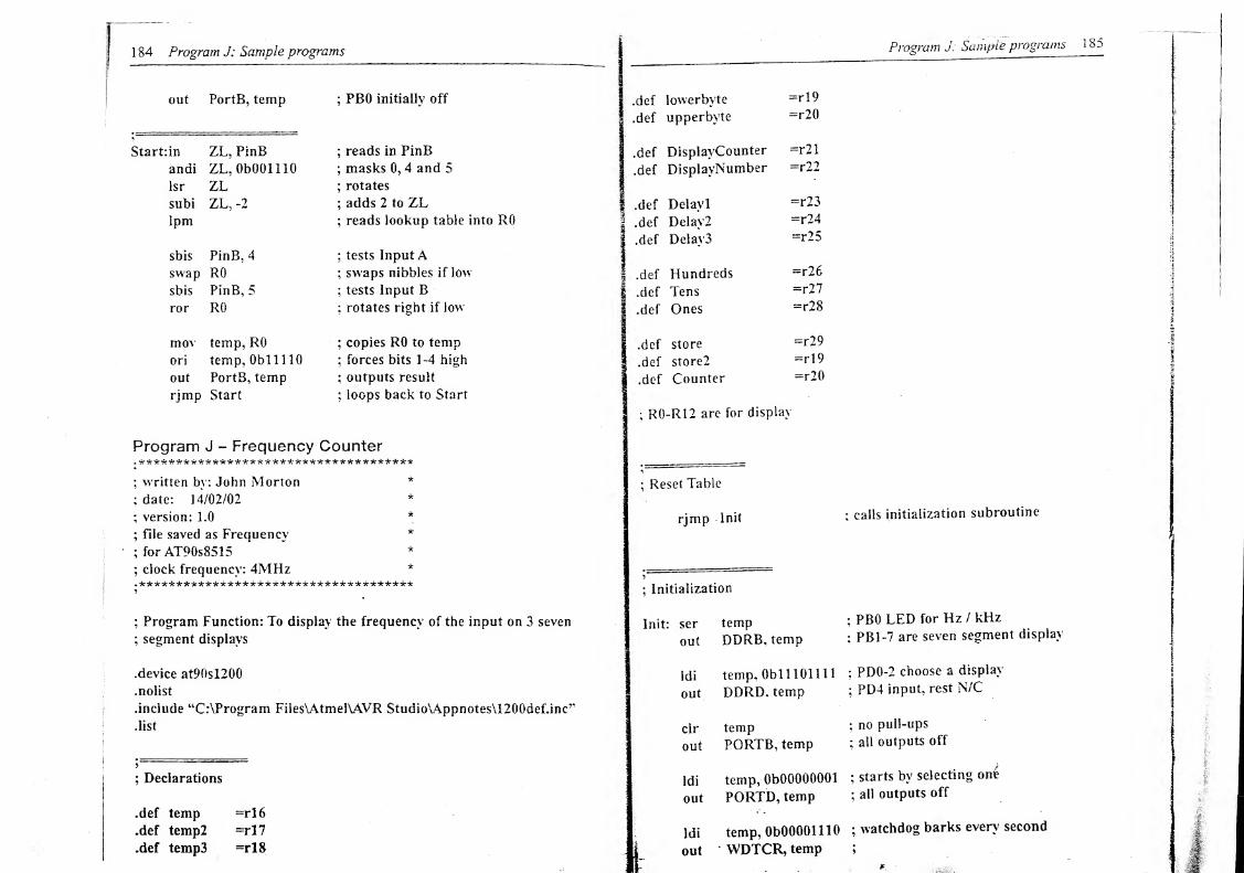
184 Program J: Sample programs
out PortB, temp
Start:in ZL, PinB
andi ZL,0b001110lsr ZLsubi ZL S
-2
lpm
sbis PinB, 4
swap ROsbis PinB, 5
ror RO
mov temp, ROori temp, Obi 11 10
out PortB, temp
rjmp Start
; PBO initially off
;reads in PinB
;masks 0, 4 and 5
; rotates
; adds 2 to ZL;reads lookup table into RO
;tests Input A
;swaps nibbles if low'
;tests Input B
;rotates right if low
; copies RO to temp
;forces bits 1-4 high
; outputs result
;loops back to Start
Program J - Frequency Counter. iricic *k jc-kic&**&&& ie icicle 1c 1c *k1c*kiricie*kik ic icicle•f
;written by: John Morton *
; date: 14/02/02 *
; version: 1.0*
; file saved as Frequency *
; for AT90s8515* *
; clock frequency: 4MHz *
.************************************
;Program Function: To display the frequency of the input on 3 seven
; segment displays
.device at90sl200
.nolist
.include wC:\Program File$\AtmelVAVR Studio\Appnotes\1200def.inc”
; Declarations
.def temp =r!6
.def temp2 =r!7
.def tempi =r!8
Program J: Sample programs 1 8d
; calls initialization subroutine
;PBO LED for Hz / kHz
: PB1-7 are seven segment display
;PDO-2 choose a display
;PD4 input, rest N1C
; no pull-ups
;all outputs off
;starts by selecting one
;all outputs off
: watchdog barks every second
* '.
'
,,, r:;
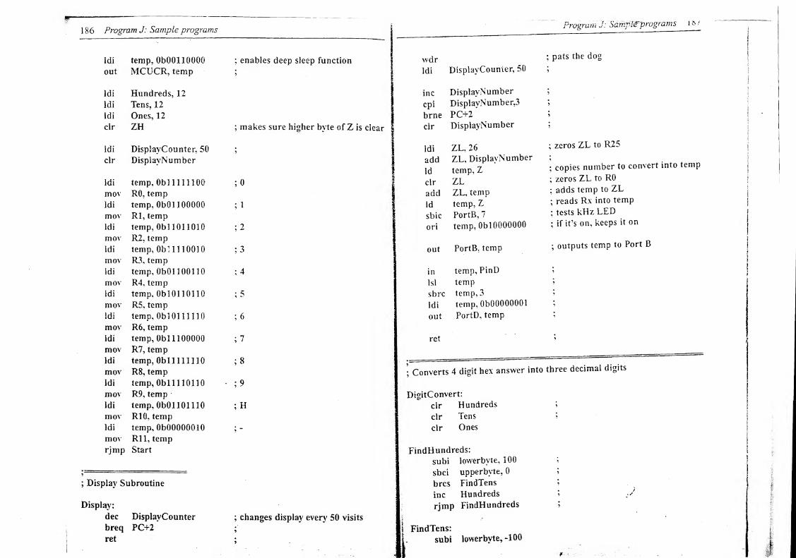
186 Program J: Sample programs
Idi temp, ObOOl 10000
out MCUCR, temp
Idi Hundreds, 12
ldi Tens, 12
Idi Ones, 12
dr ZH ;makes sure higher byte ofZ is dear
ldi DispIavCounter, 50 ;
dr DisplayNumber
idi temp, Obi 11 II 100 ;0mov R0, temp
ldi temp, ObOl 100000 ;1
mov Rl, templdi temp. Obi 101 1010 ;2
mov R2, temp
idi temp, 0b 1111 001 0 ;3mov R3, temp
ldi temp, ObOl 1001 10 ;4
mov R4, temp
ldi temp. Obi 0110110 ;5
mov R5, temp
ldi temp, Obi 0111110 ;6mov R6, temp
ldi temp, Obi 1100000 ;7mov R7, temp
ldi temp, Obi 1111110 ;8mov R8, temp
Idi temp, Obll 11 0110 - ;9mov R9, temp
ldi temp, ObOllOlllO ;Hmov R10, temp
ldi temp, ObOOOOOOlO ;-
mov Rll, temp
rjmp Start
; Display Subroutine
Display:
dec DisplayCounter; changes display every 50 visits
breq PC+2;
ret ;
Program J:~Sanrp!Wprograms i & /
wdr ;pats the dog
j
ldi DispIavCounter, 50# 1
>j
inc DisplayNumber 5
cpi DisplayNumber,
3
\
brne PC+2'clr DisplayNumber >
ldi ZL, 26 ;zeros ZL to R25
add ZL, DisplayNumber
Id temp, Z ;copies number to convert into temp
clr ZL ;zeros ZL to R0
add ZL, temp ; adds temp to ZL
Id temp, Z ;reads Rx into temp
sbic PortB, 7 ;tests kHz LED
ori temp, OblOOOOOOO ; if it’s on, keeps it on
out PortB, temp ;outputs temp to Port B
in temp, PinD
lsl temp *
sbrc temp, 3
ldi temp, ObOOOOOOOl
out PortD, temp
ret-
;
• Converts 4 digit hex answer into three decimal digits
DigitConvert:
clr Hundreds ;
clr Tens ?
clr Ones
FindHundreds:
subi lowerbvte, 100 *
sbci upperbvte, 0 ;
brcs FindTens ?
inc Hundreds 1
rjmp FindHundreds ;
t FindTens:
subi lowerbyte, -100
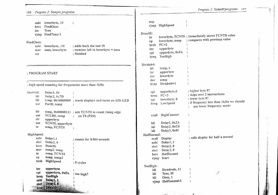
1 8 8 Program J: Sample programs
subi lowerbyte, 10
brcs FindOnes
inc Tens
rjmp FindTens+1
FindOnes:
subi lowerbyte, -10;adds back the last 10
mov ones, lowerbyte ;number left in lowerbyte = ones
ret ; finished
; PROGRAM START
; high speed counting for frequencies more than 1kHz
Startridi Delayl, 00 ;
Idi Delay2, 0x7D ;
Idi temp, OblOOOOOOO ; resets displays and turns on kHz LEDout PortB, temp :
idi temp, ObOOOOOlll;sets TCNTO to count rising edge
out TCCRO, temp;
on TO (PB4)clr upperbyteout TCNTO, upperbvtein temp, TCNTO ‘
;
Highspeed:
subi Delay 1,1 . COunts for 0.064 secondssbci Delay2,
0
brcs DoneHimov temp2, tempin temp, TCNTO •
cp temp, temp2 !
brsh Highspeed! 8 cycles
inc upperbyte
cpi upperbyte, OxFAbreq TooHigh
subi
Program J: SimpWprograms 1 sy
nop
rjmp Highspeed
lowerbyte, TCNTO ;immediately stores TCNTO value
lowerbyte, temp ;compares with previous value
PC+2 ' ;
upperbyte ;
upperbyte, OxFA ;
TooHigh ;
Divide64:
Idi temp, 6
Isr upperbyte
ror lowerbyte
dec temp
brne Divide64+1
cpi upperbyte,
0
brne PC+3
cpi lowerbyte, 0
breq LowSpeed
higher byte 0?
skips next 2 instructions
lower byte 0?
if frequency less than 1 kHz we should
use lower frequency mode
rcall DigitConvert
Idi Delay 1, 0x2
A
Idi Delav2, 0xC6
Idi Delay3, 0x01
HalfSecond:
rcall Display
subi Delayl, 1
sbci Delayl, 0
sbci Delay3,
0
brcc HalfSecond
rjmp Start
; calls display for half a second
TooHigh:
Idi
Idi
Idi
Hundreds, 11
Tens, 10
Ones, 1
rjmp HalfSecond-3
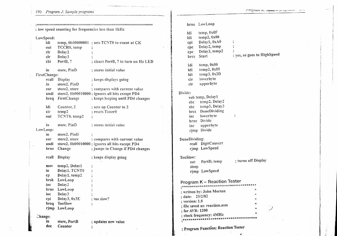
rrugram r\. ^***^..w
brne LowLoop
ldi temp, OxOF
Idi temp2, 0x00
cpi Delay 1, OxAO ; i
cpc Delav2, temp ;j
cpc Delay3, temp2 ; o ,!
brcs Start ;yes, so goes to Highspeed
j
I
ldi temp, 0x00
ldi temp2, 0x09
ldi temp3, 0x3D
clr lowerbvte
clr upperbvte
Divide:
sub temp, Delavl
sbc temp2, Delay2
sbc temp3, Delay3
brcs DoneDividing
inc lowerbvte ;
brne Divide
inc upperbvte
rjmp Divide
DoneDividing:
rcall DigitConvert
rjmp Low'Speed
TooSlow:
out PortD, temp : turns off Display
sleep
rjmp LowSpeed
Program K - Reaction Tester**************************************’ *
;written by: John Morton
; date: 25/2/02*
;version: 1.0
;file saved as: reaction.asm .
; for AVR: 1200*
: clock frequency: 4MHz.*********•****************************5
;Program Function: Reaction Tester
1 92 Program K: Sample programs
.device at90sl200
.nolist
.include “C:\Program Files\Atmel\AVR Studio\Appnotes\1200def.inc’
.list
; Declarations:
|
.def temp =r!6
.def Random =rl7
1 .def Five =rl8
l-def TimeL =rl9
1
.def TimeH =r20
1
.def Hundreds =r21
!.def Tens =r22.def Ones =r23
.def CountX =r24
.def DisplavNumber =r25
.def DisplayCounter =r26
.def tempH =r27
.def Count4 =r28
j
5? g.
j 1
!i J
Start of Program
rjmp Init
rjmp Extint
rjmp TCNTOInt
; First line executed
Extint:
sbis PinD, 0; tests LED
rjmp Cheat>
dr temp; stops TCNTO
out TCCROin TimeL, TCNTO
; reads in TCNTO valuein temp, TIFR
; test for TCNTO overflowsbrc temp, 1
inc TimeH9
subi TimeL, 0xA2; subtracts back 0xA2 from
sbci TimeH, 0; total reaction time
ldi temp, ObOOOOOlOl; restarts TCNTO at CK/1024
out TCCRO, temp5
ldi Count4,
4
; Multiplies reaction time
Program K: SaTnple programs 1 ^3
mov temp. TimeL ;by Five
mov tempH, TimeH ;
TimesS:
add temp. TimeL ;
adc tempH, TimeH ;
dec Count4 ;
brne TimesS >
clr TimeL 5
clr TimeH
Dividel2:
subi temp. 12 ;
sbci tempH. 0 ;j
brcs DoneDividing;
j
inc TimeL ;
brne Dividel2 \
inc TimeH ;
rjmp Dividel2 ;
DoneDividing:
rcall DigitConvert :
rct ; returns DOESN'T enable interrupts
Cheat:
ldi Hundreds, 10 ;b
ldi Tens, 11 ; A
ldi Ones, 12 ;d
ret ;returns and DOESN’T enable interrupts
TCNTOInt:
sbic PinD. 0 ?tests LED
rjmp TInt_LEDon :
dec CountX ;
breq PC-r2 ;
reti
ldi temp. 0xA2 ;
out TCNTO, temp ;
sbi PortD, 0 ; turns on LEDreti ? j
TInt_Ledon:
inc TimeH
cpi TimeH, OxOA
breq PC-r2
;increments higher byte
; tests for maximum time
; skips if too slow
m~I 194 Program K: Sample programs
reti
ldi Hundreds, 13 9
Idi Tens, 14 ; hIdi Ones, 1 ; i
ret 9
Display Subroutine
Display:
dec DisplayCounter ;changes display every 50 visits
breq P02*
ret 9
wdr ;pats the dog
ldi DisplayCounter, 50 9
inc DisplayNumber 9
cpi DisplayNumber,
3
5
brne PC+2 9
clr DisplayNumber 9
Idi ZL, 21 ; zeros ZL to R2I
add ZL, DisplayNumber 9
Id temp, Z ;copies number to convert into temp
Idi ZL, 0 ; zeros ZL to R0add ZL, temp
;adds temp to ZL
id temp, Z ; reads Rx into temp
out PortB, temp ;outputs temp to Port B
brtc PC+2 ; tests T bit
sbi PortB, 0 ; turns on kHz LED
in temp, PinD 9
Isl temp 9
brcs PC+2 9
ldi temp, ObOOlOOOOO 9
ori temp, ObOOOOOllO
out PortD, temp 9
ret 9
Converts 4 digit hex answer into three decimal digits
|DigitConvert:
Program K: Sample programs
clr Hundreds '>
clr Ones 1
clr Tens 5
FindHundreds:
subi TimeL, 100 »
sbci TimeH, 0 >
brcs FindTens ?
inc Hundreds ;
rjmp FindHundreds ;
FindTens:
subi TimeL, -100
subi TimeL, 10
brcs FindOnes
inc Tens
rjmp FindTens+1
FindOnes:
subi TimeL. -1
0
mov Ones, TimeL
ret
: adds back the last 10
;number left in lowerbvte = ones
: finished
lnit: ldi temp, Obllllllll ; PB1-7: outputs, PB0: N/C
out DDRB, temp ; _ N/rldi temp, Obi 111 1001 ; PDO.4-6: outputs, PD3,7: N/C
out DDRD, temp ;PD1,2: inputs
ldi temp, ObOOOOOOOO ;
out PortB. temp ;
ldi temp. ObOOlOOllO ;selects first display, pull-ups
out PortD, temp 5on both buttons
ldi temp, ObOOOOOlOl ;TCNT0 at CK/1024
out TCCR0, temp ;
ldi temp, ObOOOOOOOO ;INTO interrupt on falling edge
out MCUCR, temp ;•/
ldi temp, ObOl000000 ;enables INTO interrupt
out GIMSK, temp ;
1 96 Program K: Sample programs
Idi temp, ObOOOOOOlO ; enables TCNTO interrupt
out TIMSK, temp;
ldi DisplayCounter, 50 ;
clr DisplayNumber
idi temp, Obll 11 1100 ;0
Imov R0, temp
idi temp, ObOl 100000 ;1
mov Rl, temp
!idi temp, ObllOl 1010 ;2mov R2, temp
idi temp. Obi 111 001 0 ;3mov R3, temp
I idi temp, ObOl 1001 10 ;4
;
mov R4, temp
|
ldi temp. Obi 01 101 1 0 ;5
j
mov R5, temp
Ildi temp. Obi 0111110 :6
1 mov R6. temp
]
ldi temp. Obi 1100000 :7
mov R7, temp
ldi temp. Obi 11 11110 ;S
mov R8, temp
ldi temp. Obi 1110110 ; 9
mov R9, temp
idi temp, ObOOl 11110 ;bmov R10, temp
j
ldi temp. Obi 1 101110 ;Amov Rll.templdi temp, ObOl 111010 ;dmov R12, temp
n body of program:
rcall Display;keeps display going
sbic PinD, 1 ; waits for Ready button
rjmp Start;keeps looping until it’s pressed
;gets next random number
mov temp, Random; multiplies by 5 and...
add Random, temp;
add Random, temp;
Program L: Sample programs 197
i
i add Random, temp 5
add Random, temp 9
inc Random ;...adds 1
mov CountX, Random 9
lsr CountX ;divides by 2 and adds 60
subi CountX, -60 9
ldi temp, ObOl00000 ;resets INTO interrupt flag
out GIFR• resets TC0 overflow interrupt flag
ldi temp, ObOOOOOOlO
out
sei
TIFR 9
;enables interrupts
clr TimeH ;reset time register
out PortB, TimeH ;also turns off displays while waiting
Loopv: , . ,
brid Start ;skips out when interrupts disabled
rjmp Loopy ; Loops
Program L - 4-bit Analogue to Digital Converter.*************************************
;written by: John Morton
; date: 25/2/02*
;version: 1.0
;file saved as: atod.asm
;for AVR: 1200
*
;clock frequency: 4MHz
*
.t************************************9
;Program Function: 4-bit A-D converter
.device at90sl200
!Include “C:\Program FilesUtmelVAVR Studio\Appnotes\1200def.inc”
.list
9~
: Declarations:7 v
,/
.def temp =rl6
Start of Program
1 98 Program L: Sample programs
rjmp Init ; first line executed
Init: Idi temp. Obi 1 111100 ; PB0,1: Analogue inputs
out DDRB, temp; PD2-7: N1C
Idi temp, Obllllllll ; PDO-3: outputs, PD4-7: N/Cout DDRD, temp ?
clr temp
out PortB, temp;
Idi temp, ObOOOOlOOO; selects msb
out PortD, temp
Idi temp, OblOOOOOOO;turns on Analogue comparator
out ACSR, temp
; Main body of program:
Start'.sbis ACSR, 5 ; checks AC result
cbi PortD, 3 ; clears bit 3
sbi PortD, 2 •>
sbis ACSR, 5;checks AC result
cbi PortD, 2 ; qlears bit 2
sbi PortD, 1
sbis ACSR, 5 ;checks AC result
cbi PortD, 1;clears bit 1
sbi PortD, 0 >
sbis ACSR, 5;checks AC result
cbi PortD, 0;clears bit 0
in temp, PortD;read in final answer
swap temp ; swap
out PortB, temp; outputs
rjmp Start ; keeps looping until it’s pressed
Program M: Sample programs 1 99
PROGRAM M - Voltage Inverter,*************************************r
;written by: John Morton *
;date: 25/2/02
*
;version: 1.0 .
; file saved as: inverter.asm*
; for AVR: 1200*
; clock frequency: 4MHz *
• ********************“**"*******’*'********
;Program Function: Outputs 5 - (input voltage)
.device atTinylS
.nolist
.include “C:\Program FilesUtmelVAVR Studio\Appnotes\Tnl5def.inc”
.list
;Declarations:
.def temp =rl6
.def tempH =rl7
.def Desired —rl 8
.def Actual =r!9
;Start of Program
rjmp Init ;first line executed
Init: Idi temp, ObOlllOO ;PB0,1,5: Inputs
out DDRB, temp ; PB2-4: N/C
clr temp ; no pull-ups
out PortB, temp
Idi temp, Obi 11 01 Oil ;enables ADC, clock = CK/8
out ADCSR, temp
clr temp ;selects ADCO, VCC as reference
out ADMUX, temp ; no left adjusted >
5
;Main body of program:
Start: cbi ADMUX, 0 ; selects ADCO input
200 Program N: Sample programs
sbi ADCSR,ADSC : starts conversion
sbic ADCSR^ADSCrjmp Start+2
in Desired, ADCH ;reads in 8-bitADC result
com Desired ; takes 5 - answer
sbi ADMUX, 0 ;selects ADC1 input
sbi ADCSR, ADSC ; starts conversion on output
Wait: sbic ADCSR,ADSC ; waits until conversion has finished
rjmp Wait
in Actual, ADCHcp Actual, Desired
brio TooLowcp Desired, Actual
brio TooHigh
cbi DDRB, 0
rjmp Start
reads in ADC result of actual output
compares actual with desired
too low?
too high?
just right, so makes PBO an input
reads ADCO input again
TooLow:
sbi DDRA, 0 : too low so makes PBO an output
sbi PortB, 0 : and sets it
rjmp Start ; reads ADCO input again
TooHigh:
sbi DDRB, 0 ;too high, so makes PBO an output
cbi PortB, 0 ; and clears it
rjmp Start; reads ADCO input again
PROGRAM N - Melody Maker**************************************
;written by: John Morton *
; date: 22/3/02 *
; version: 1.0 *
;file saved as: music.asm *
;for AVR: 2313 *
; clock frequency: 4MHz *
**************************************9
; Program Function: Plays a melody stored in the EEPROM
.device at90s2313
.nolist a*
202 Program N: Sample programs
out PortD, temp
reti
ChangeNote:
dec Length ; waits sufficient length
breq PC-r-29
reti 9
Rest: in temp, TIFR;creates short pause between notes
sbrs temp, 1 9
rjmp Rest '
9
ldi temp, ObOOOOOOlO ;
out TIFR, temp9
Read_EEPROM:out EEARL, address ; reads next address
sbi EECR, 0 ; initiate read
;get note
in ZL. EEDR : reads EEPROMandi ZL, ObOOOOl 111 ; masks bits 4-7
cpi ZL, OxOC : if OxOC, loops back to first address
breq Reset *
brio PC+2 ; if higher than 0C, makes OBldi ZL, OxOB 9
lsl ZL ;multiplies by 2 to get word address
subi ZL, -0x26 ; adds 26 to point to table
1pm ; reads look-up table
mov NoteL, R0;stores result
inc ZL; reads next entry of look-up table
1pm
mov NoteH, R0 ;stores result
;get octave
in temp, EEDR;reads EEPROM again
swap temp 9
andi temp, ObOOOOOOll;gets bits 4 and 5
GetOctave:
breq GetLength ; uses bits 4,5 to select octave
lsl NoteL; divides by two to get next octave
1
rol NoteH 9
Program N: Sample programs 203i
dec temp
rjmp GetOctave
GetLength: ;gets length
out OCR1AH, NoteH ; stores final freq values in Output
out OCR1AL, NoteL ;Compare registers
in temp, EEDR ;reads EEPROM again
andi temp, ObllOOOOOO;gets bits 6 and 7
swap temp ;
Isr temp ;uses these to get a Length = 2, 4, 6 or 8
subi temp, -2 ;
mov Length, temp ; stores in Length
inc address ;selects next EERPOM address (next note)
reti
Reset:
cir address ; resets EEPROM address to 0
rjmp Read_EEPROM ;
Init: ldi temp. ObOlOOOOOO
out DDRB, temp
idi temp, ObOl 1 11011
out DDRD, temp
ldi temp, OblOOOOOOO
out PortB, temp
ldi temp, ObOOOOOlOO
out PortD, temp
ldi temp, ObOOOOOlOl
out TCCRO, temp
dr temp
out TCCR1A, temp
ldi temp, ObOOOOlOOl
out TCCR1B, temp
ldi temp, ObOlOOOOlO
out TIMSK, temp
ldi temp, ObOOOOOOOO
out GIMSK, temp
ldi temp, RAMENDout SPL, temp
; PBO-5: keyboard in
; PB6: N/C, PB7: Record
; PDO: N/C, PD1: speaker
; PD2: play, PD3-6: keyboard out
;no pull-ups on PortB
9
;pull-ups on play button
; TCO is CK/1024
;no PWM
; TCI is CK, clear TCI
; after comparematch
;enables TCO interrupt
; enables TCI CompAdnt.
; disables other interrupts
; sets up stack pointers
¥;
..
204 Program O: Sample programs
clr ZH ;
clr address ;
out EEARH, address ;
rcall Read_EEPROM ;gets first note
;Main body of program:
Start:rjmp Start
PROGRAM O - Keyboard Converter. ******************** **************** *
; written by: John Morton *
: date: 25/2/02 *
; version: 1.0*
; file saved as: Keyboard.asm *
; for AVR: 2313* *
: clock frequency: 4MHz *
• 'k-k ikjc'k'k'k-kic1:'k'k*icJc1c'k'kicik*k'k'k'k'k-k'k'k'k*'kJc4:'k'k'k-k*
; Program Function: Converts a computer keyboard into a musical one
.device at90s2313
.nolist
.include “C:\Program Files\Atmel\AVR Studio\Appnotes\2313def.inc”
.list
; Declarations:
.def temp =rl6
.def data =rl7
.def Length =r!8
; Start of Program
rjmplnit
reti
reti
reti
reti
reti
; first line executed
; S001 - INTO
; S002
; S003
; S004 - Compare A; $005
Program O: Sample programs 205
reti » S006 - TCI Overflow
rjmp EndNote l S007 - TC0 Overflow
reti 5S008
rjmp Change ; S009 - UART Received
reti ; S00A
reti S00B
reti 5sooc
•>
.org 13
;Note Lookup Table
.dw 0x1 E84 ‘a’ = C
.dw OxFFFF, OxFFFF ‘b\ ‘c’ = nothing
.dw 0x1838 ‘d’ = E
.dw Oxl 9A9 ‘e’ = D#
.dw 0xl6DC ;‘r=F
.dw 0x1 45E ;‘g’ = G
.dw 0x1225 ;‘h’ = A
.dw OxFFFF ;T = nothing
.dw 0x1 02A :‘j' = B
.dw 0x0F42 ;‘k' = C hi
.dw 0x0D98 ;T = D hi
.dw OxFFFF, OxFFFF ;
km\‘n’= nothing
.dw 0x0E67 ;‘o’ = C# hi
.dw 0x0CC8 ;‘p’ = D# hi
.dw OxFFFF, OxFFFF ;‘q’, ‘r’ = nothing
.dw 0x1 B30 ;‘s’ = D
.dw 0x1594 ;‘t’ = F#
.dw 0x1120 ;
ku’ = A#
.dw OxFFFF :‘v’ = nothing
.dw 0x1CCE ;‘w’ = C#
.dw OxFFFF ;‘x’ = nothing
.dw 0x1339 ;‘y’ = G#
.dw OxFFFF ;
kz’ = nothing
.dw OxFFFF ;26 = nothing
.org 43
;Seven-segment Lookup Table
,/i
.db ObOlllOOOl ;C
.db Obi 0000000, OblOOOOOOO ; dash
.db ObimOOOl ;E
.db OblOUlllO ;d#
.db OblllOOOOl ;F
.db ObOl 110101
.db Obi 11001 11 ;A
.db OblOOOOOOO ;dash
.db ObllllOlOO ;b
.db ObOl 110001 ;c
.db OblOllOllO ;d
.db OblOOOOOOO, OblOOOOOOO ;dash
.db ObOl 11 1001 ;C#
.db Obi 01 11110 ;d#
.db OblOOOOOOO, OblOOOOOOO ;dash
.db OblOllOllO ;d
.db Obi 1101001 ;F#
.db Obi 1101 111 ;A#
.db OblOOOOOOO ; dash
.db ObOl 11 1001
.db OblOOOOOOO ;dash
.db ObOl 111101 ;G#
.db Ob 10000000, Obi 0000000
9
EndNote:
clr temp
out TCCR1A, temp
reti
; dash
9
9
Change:
in ZL, UDRsubi ZL, 0x61
cpi ZL, 26
brio PC+2ldi ZL, 26
Is! ZLsubi ZL, -27
Ipm
out OCR1AH, ROdec ZL1pm
out OCR1AL, RO
subi ZL, -60
1pm
;reads data
;subtracts 0x61
;if ZL is more than 25
;makes ZL = 26
;multiples ZL by 2
;adds 27, points to higher byte
;reads higher byte
; stores in OCR1AH;points to lower byte
; reads lower byte
;stores in OCR1AL
;points to second lookup table
;reads table
out PortB, RO ; displays result
mov temp, RO;copies R0 to temp
andi temp, ObOQOOJOOO;masks all but bit 3
out PortD, temp; copies to PortD to set # LED
ldi temp, ObOl 000000 ; OC1 toggles with each Outputout TCCR1A, temp
; Compare interrupt
clr temp; resets TCNTO
out TCNTO 9
reti9
ser temp; 7 seg code
out DDRB, temp; PB6: N/C, PB7: Record
ldi temp. Obi 1111110 ; PD0: RXDout DDRD, temp
; PD1: TXD
clr temp; no pull-ups on PortB
out PortB, temp
out PortD, temp9
ldi temp, ObOOOOOlOl; TC0 is CK/1024
out TCCRO, temp9
ldi temp, ObOlOOOOOO; no PWM
out TCCR1A, temp9
ldi temp, ObOOOOlOOl; TCI is CK, clear TCI
out TCCR1B, temp; after compare match
ldi temp, ObOlOOOOlO ; enables TC0 interrupt
out TIMSK, temp; enables TCI CompA int.
ldi temp, ObOOOOOOOO ; disables other interrupts
out GIMSK, temp 9
ldi temp, RAMENDout SPL, temp
ldi temp, 15 ; baud rate = 9600out UBRR, temp 9
ldi temp, OblOOlOOOO ; enables RX mode and RX interrupt
out UCR, temp 9
ldi NoteH, OxlE ; plays a C when first turned on
ldi NoteL, 0x84 $ *
out OCR1AH, NoteH 9
y
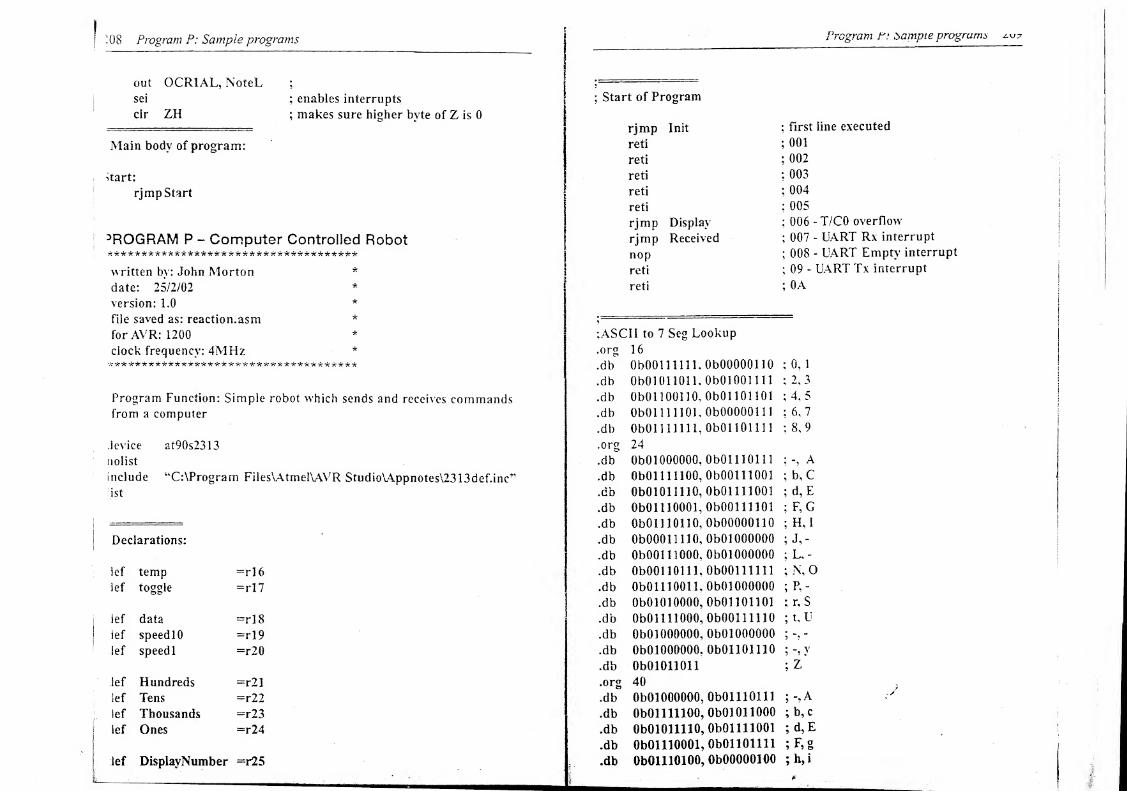
f
'08 Program P: Sample programs
out OCR1AL, NoteL ;
sei ; enables interrupts
clr ZH ; makes sure higher byte of Z is 0
Main body of program:
^tart:
rjmp Start
PROGRAM P - Computer Controlled Robot***************** * ********** -k * -k -k* It -k**
written by: John Morton *
date: 25/2/02 *
version: 1.0 *
file saved as: reaction.asm *
for AYR: 1200 *
clock frequency: 4MHz *
*************************************
Program Function: Simple robot which sends and receives commandsfrom a computer
device at90s2313
nolist
include “C:\Program Files\AtmeI\AVR Studio\Appnotes\2313def.inc”
ist
Declarations:
ief temp =rl6
lef toggle =rl7
ief data =rl8
ief speedlO =rl9
ief speedl =r20
Jef Hundreds =r21
ief Tens =r22
lef Thousands =r23
ief Ones =r24
lef DisplayNumber =r25
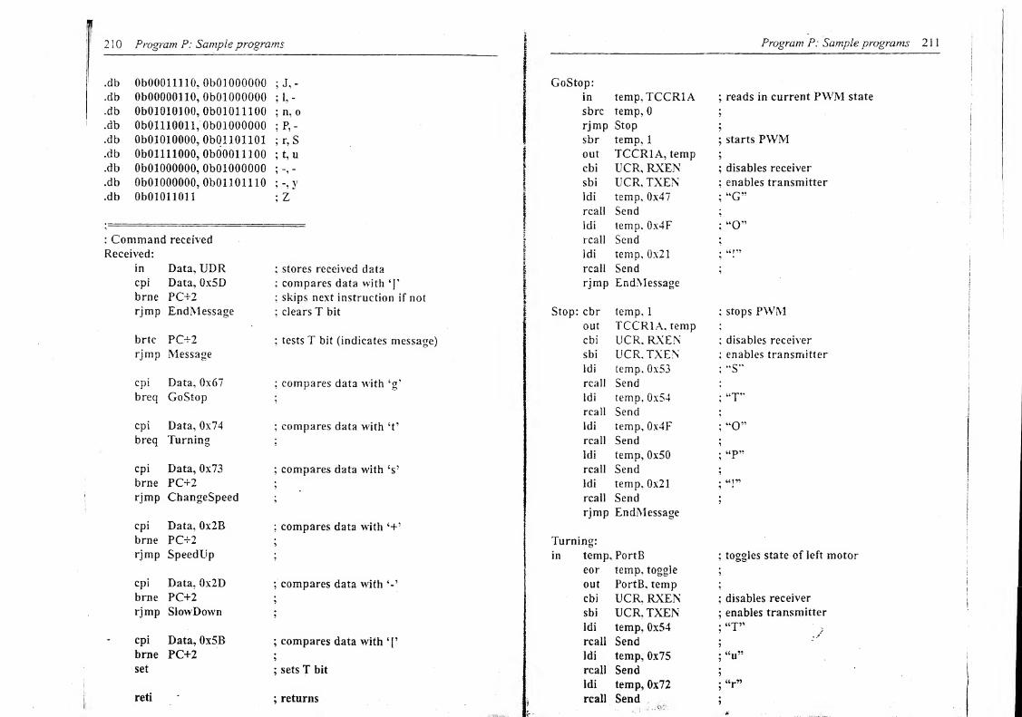
2 1 0 Program P: Sample programs
.db ObOOOllllO, ObOlOOOOOO; J,-
.db ObOOOOOllO, ObOlOOOOOO; i, -
.db ObOlOlOlOO, ObOlOlllOO; n, o
.db ObOlllOOll, ObOlOOOOOO ;P,-
.db ObOlOlOOOO, ObOllOllOl ; r, S
.db ObOllllOOO, ObOOOlllOO ; t, u
.db ObOlOOOOOO, ObOlOOOOOO 7 “7 “
.db ObOlOOOOOO, ObOllOlllO; -,y
.db ObOlOl 1 01
1
;Z
; Command received
Received:
in Data, UDR : stores received data
cpi Data, 0x5D : compares data with ‘fbrne PC+2 : skips next instruction if not
rjmp EndMessage; clears T bit
brtc
rjmp
PC+2Message
;tests T bit (indicates message)
cpi Data, 0x67;compares data with ‘g’
breq GoStop7
cpi Data, 0x74 : compares data with ‘t’
breq Turning5
cpi Data, 0x73;compares data with ‘s’
brne PC+2?
rjmp ChangeSpeed?
cpi Data, 0x2B : compares data with ‘+’
brne PC+27
rjmp SpeedUp;
cpi Data, 0x2D; compares data with
brne PC+2 J
rjmp SlowDownr
cpi Data, 0x5B; compares data with
brne
set
PC+27
; sets T bit
reti*
; returns
Program P: Sample programs 2 1
1
GoStop:
in temp, TCCR1A ; reads in current PWM state
sbrc temp, 0 5
rjmp Stop
sbr temp, 1 ; starts PWMout TCCR1A, temp
cbi UCR, RXEN ; disables receiver
sbi UCR, TXEN ;enables transmitter
ldi temp, 0x47 ; “G”rcall Send :
ldi temp, 0x4F
rcall Send
ldi temp, 0x21 } •
rcall Send 7
rjmp EndMessage
Stop: cbr temp, 1 ; stops PWMout TCCR1A, temp ;
cbi UCR, RXEN ; disables receiver
sbi UCR, TXEN ; enables transmitter
ldi temp, 0x53 ; "S*
rcall Send *
ldi temp, 0x54 ; “T”rcall Send 7
ldi temp, 0x4F
rcall Send
ldi temp, 0x50 ; “P”
rcall Send 7
ldi temp, 0x21 . it f77
7
rcall Send7
rjmp EndMessage
Turning:
in temp.,PortB ; toggles state of left motor
eor temp, toggle 7
out PortB, temp ;
cbi UCR, RXEN ;disables receiver
sbi UCR, TXEN ;enables transmitter
ldi temp, 0x54 . U’T’77’ ^ /
rcall Send 7
ldi temp, 0x75 ; “u”
rcall Send 7
ldi temp, 0x72 ;“r”
rcall Send 5
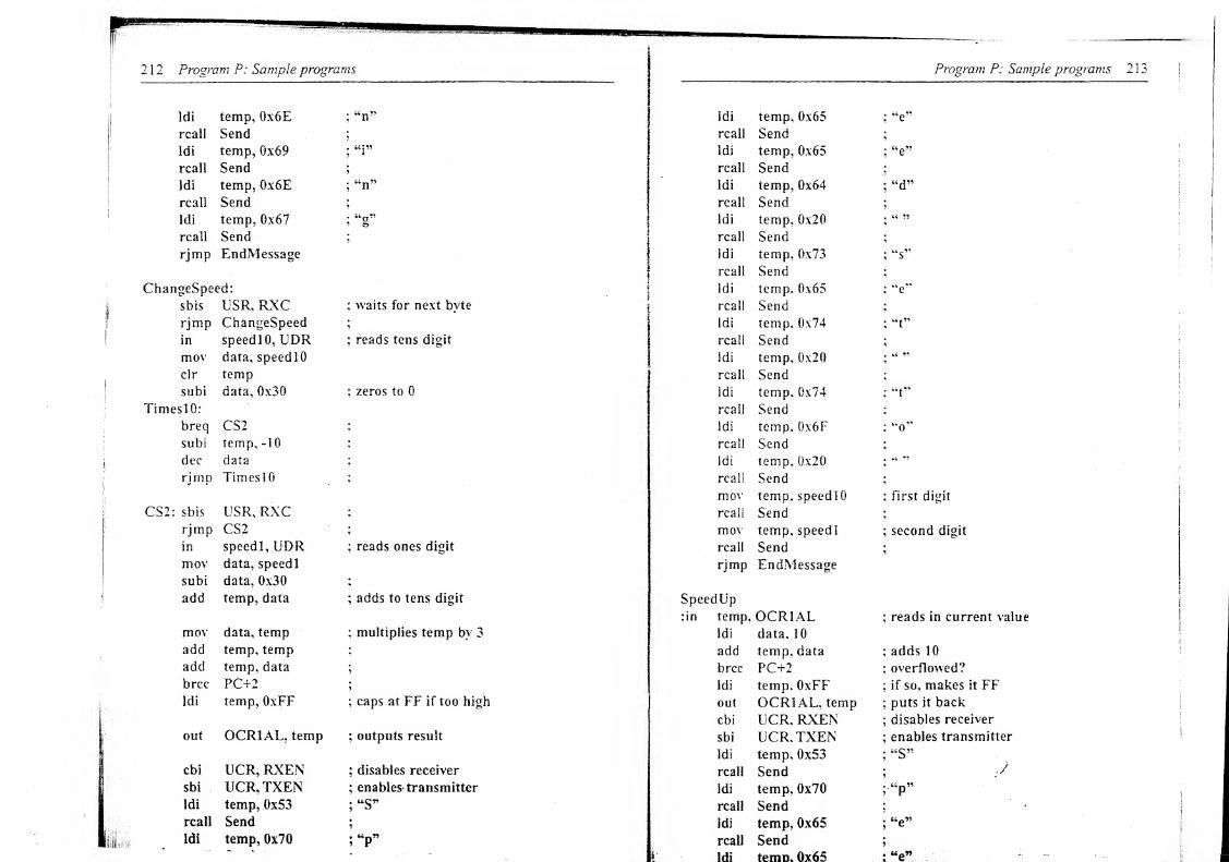
2 1 2 Program P: Sample programs Program P: Sample programs 2 1
3
ldi temp, 0x6E ; “n” ldi temp, 0x65 : “e”
rcall Send i rcall Send 7
ldi temp, 0x69 ?1 ldi temp, 0x65 ; “e”
rcall Send rcall Send :
ldi temp,<h;6E ; “n” ldi temp, 0x64;“d”
rcall Send 7 rcall Send?
ldi temp, 0x67 • “o”* to
ldi temp, 0x20 . « 75
,
rcall Send : rcall Send 7
rjmp EndMessage!
idi temp, 0x73 .
7 S
!, rcall Send ;
ChangeSpeed: Idi temp. 0x65 : “e”
sbis USR, RXC ;waits for next byte rcall Send
rjmp ChangeSpeed 7 idi temp. 0x74 . *.i|-77
in speedlO, UDR : reads tens digit rcall Send 7
mov data, speedlO idi temp, 0x20 . U 77
7
clr temp rcall Send 1
subi data, 0x30 ; zeros to 0 Idi temp. 0x74 . Uj7*
TimeslO: rcall Send *
breq CS2 * ldi temp. 0x6F : “o’*
subi temp, -10 ; rcall Send 1
dec data ldi temp, 0x20 . »• 77
rjmp TimeslO , rcall Send l
mov temp, speedlO : First digit
CS2: sbis USR, RXC ; rcall Send *
rjmp CS2 ; mov temp, speedl; second digit
in speedl, UDR ; reads ones digit rcall Send 7
mov data, speedl rjmp EndMessagesubi data, 0x30 *>
add temp, data ; adds to tens digit SpeedUp:in temp, OCR1AL ;
reads in current value
mov data, temp ; multiplies temp by 3 ldi data, 10
add temp, temp add temp, data ; adds 10
add temp, data; brcc P02 : overflowed?
brcc PC+2 idi temp, OxFF ;if so, makes it FF
ldi temp, OxFF : caps at FF if too high out OCR1 AL, temp;puts it back
cbi UCR, RXEN ;disables receiver
out 0CR1AL, temp ;outputs result sbi UCR, TXEN ;
enables transmitter
ldi temp, 0x53 ; “S”cbi UCR, RXEN ; disables receiver rcall Send ; ysbi UCR,TXEN ; enables- transmitter ldi temp, 0x70 ;“p”
ldi temp, 0x53 ; “S* rcall Send I
rcall Send 5 ldi temp, 0x65 ;“e”
ldi temp, 0x70 ;“p” rcall Send 5*
-
t ldi temn. 0x65 : “e”
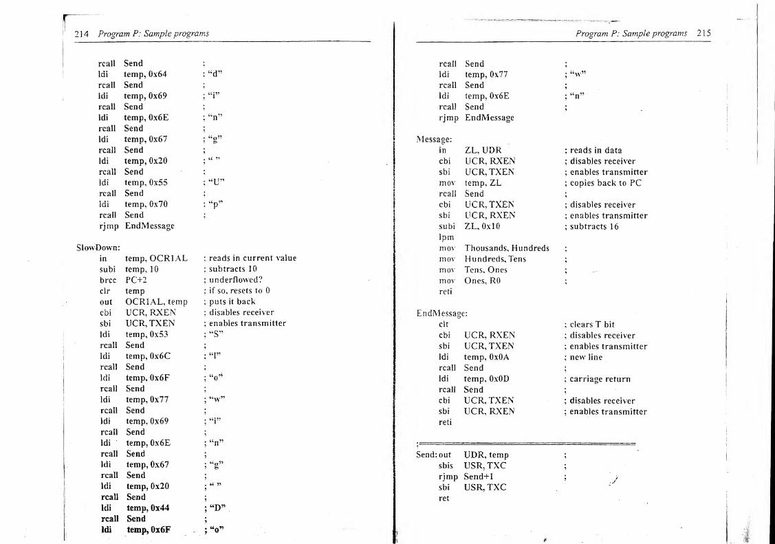
2 1 4 Program P: Sample programs Program P: Sample programs 21
5
rcall Send 9 rcall Send 9
ldi temp, 0x64 ;“d” ldi temp, 0x77
;“w”
rcall Send ? rcall Send 9
ldi temp, 0x69 ;“i” ldi temp, 0x6E ; “n”
rcall Send : rcall Send9
ldi temp, 0x6E ;“n” rjmp EndMessage
rcall Send |
ldi temp, 0x67 Message:
rcall Send 9 in ZL, UDR ;reads in data
ldi temp, 0x20 . (( 79
9 .cbi UCR, RXEN : disables receiver
rcall Send • sbi UCR, TXEN ; enables transmitter
ldi temp, 0x55 : “U” mov temp, ZL;copies back to PC
rcall Send • rcall Send 9
ldi temp, 0x70 :“p" cbi UCR, TXEN ; disables receiver
real! Send ; sbi UCR, RXEN ; enables transmitter
rjmp EndMessage subi ZL. 0x10 ; subtracts 16
1pm
SlowDown: mov Thousands, Hundreds 9
in temp, OCR1AL ; reads in current value mov Hundreds, Tens 9
subi temp, 10 ;subtracts 10 mov Tens, Ones ,
—
’
brcc PC+2 ;underflowed? mov Ones, R0
clr temp : if so, resets to 0 reti
out OCR1AL, temp;puts it back
cbi UCR, RXEN ;disables receiver EndMessage:
sbi UCR, TXEN ;enables transmitter clt
;clears T bit
ldi temp, 0x53 ;“S” cbi UCR, RXEN ; disables receiver
rcall Send 9 sbi UCR, TXEN ; enables transmitter
ldi temp, 0x6C . «|99ldi temp, OxOA ; new' line
rcall Send 9 rcall Send 9
ldi temp, 0x6F ;“o” ldi temp, OxOD ; carriage return
rcall Send 9 rcall Send 9
ldi temp, 0x77 ;“w” cbi UCR. TXEN ; disables receiver
rcall Send 9 sbi UCR, RXEN ; enables transmitter
ldi temp, 0x69 . «j99reti
rcall Send ;
ldi temp, 0x6E;“n" — —
rcall Send 9 Send: out UDR, temp i
ldi temp, 0x67 . Uct
99
9 fc> sbis USR.TXC 9
rcall Send 9 rjmp Send+19 /
ldi temp, 0x20 . U 99
9 sbi USR, TXCrcall Send 9 ret
ldi temp, 0x44 ; “D”rcall Send 9
ldi temp, 0x6F ;
wO”r
I*
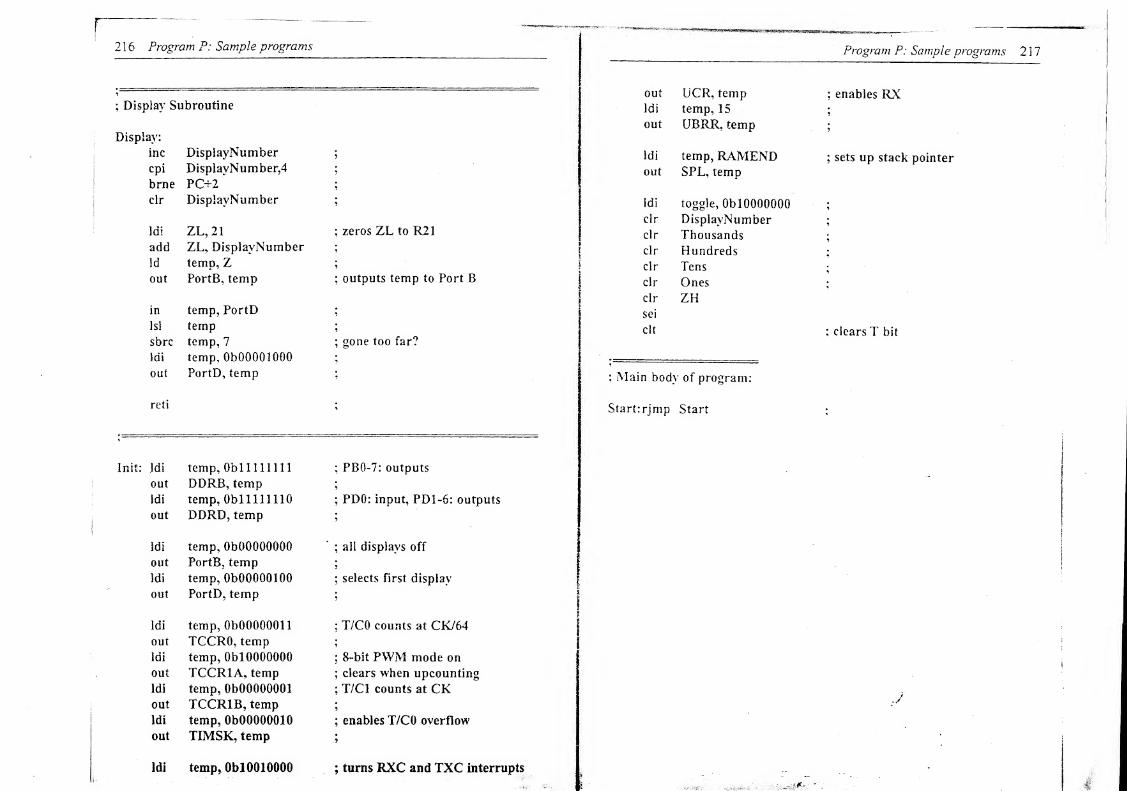
; Display Subroutine
Display:
inc DisplayNumber 5
cpi DisplayNumber,4 9
brne PC+2 9
clr DisplayNumber 9
Idi ZL, 21 ; zeros ZL to R21
add ZL, DisplayNumber
Id temp, Zout PortB, temp ;
outputs temp to Port B
in temp, PortD ?
i si temp 9
sbrc temp, 7;gone too far?
Idi temp, ObOOOOlOOO :
out PortD, temp :
lnit: Idi temp. Obi 1111111 ; PBO-7: outputs
out DDRB, tempidi temp, Obi 1111 110 ; PD0: input, PD1-6: outputs
out DDRD, temp 9
Idi temp, ObOOOOOOOO ’
; ail displays off
out PortB, temp
Idi temp, ObOOOOOlOO;selects first display
out PortD, temp9
idi temp, ObOOOOOOll; T/C0 counts at CK/64
out TCCRO, temp9
Idi temp, OblOOOOOOO;8-bit PWM mode on
out TCCR1A, temp;clears when upcounting
Idi temp, ObOOOOOOOl ; T/Cl counts at CKout TCCR1B, temp
9
Idi temp, ObOOOOOOlO;enables T/C0 overflow
out TIMSK, temp.9
Idi temp, Obi 0010000; turns RXC and TXC interrupts
Program P: Sample programs 217
out UCR, temp; enables RX
Idi temp, 159
out UBRR, temp9
Idi
out
temp, RAMENDSPL, temp
; sets up stack pointer
Idi toggle, OblOOOOOOO9
clr DisplayNumber9
clr Thousands9
clr Hundredsclr Tens
9
clr
clr
sei
clt
Ones
ZH9
; clears T bit
: Main body of program:
Start: rjmp Start
Answers to exercises
Answers to Chapter 1
Answer 1.1: (a)
Largest power of two less than 199 = 128 = 2'. Bit 7 = 1
This leaves 199 - 128 = 71. 64 is less than 71 so bit 6 = 1
This leaves 71 - 64 = 1. 32 is greater than 7 so bit 5 = 0
16 is greater than 7 so bit 4 = 0
8 is greater than 7 so bit 3 = 0
4 is less than 7 so bit 2 = 1
This leaves 7-4 = 3. 2 is less than 3 so bit 1 = 1
This leaves 3-2=1. 1 equals 1 so bit 0 = 1
The resulting binary number is: 11000111
OR...
(b)
Divide 199 by two
Divide 99 by two.
Divide 49 by two.
Divide 24 by two.
Divide 12 by two.
Divide 6 by two.
Divide 3 by two.
Divide 1 by two.
So 11000111 is the binary equivalent.
Answer 1.2 : (a)
Largest power of two less than 170 = 128 = 2 /. Bit 7 = 1
This leaves 170 - 128 = 42. 64 is greater than 42 so bit 6 = 0
32 is less than 42 so bit 5 = 1
This leaves 42 - 32 = 10. 16 is greater than 10 so bit 4 = 0
8 is less than 10 so bit 3 = 1
This leaves 10-8 = 2. 4 is greater than 2 so bit 2 = 0
2 equals 2 so bit 1=1Nothing left, so bit 0 = 0
The-resulting binary number is: 10101010
Leaves 99. remainder 1
Leaves 49, remainder 1
Leaves 24, remainder 1
Leaves 12, remainder 0
Leaves 6, remainder 0
Leaves 3, remainder 0
Leaves 1 , remainder 1
Leaves 0, remainder 1
Answers to exercises 2 1
9
OR...
Leaves 85, remainder 0
Leaves 42, remainder 1
Leaves 21, remainder 0
Leaves 1 0, remainder 1
Leaves 5, remainder 0
Leaves 2, remainder 1
Leaves 1, remainder 0
Leaves 0, remainder 1
So 10101010 is the binary equivalent.
Answer 1.3
:
There are twelve 16s in 199. leaving 199 - 192 = 7.
So bit 1 = 12 = C, and bit 0 = 7. The number is therefore: Cl.
Answer 1.4: There are ten 16s in 170. leaving 170 - 160 = 10. So bit 1 = A,and bit 0 = 10 = A. The number is therefore : AA .
Answer 1.5: 1 1 10 = 14 = E. 0111=7.The number is therefore E7.
Answer 1.6: 1111
01011010 =90+ 00001111 = 15
01101001 =105
Answer 1.7: 40 = 00 1 0 1 000 50 = 00 1 1 00 1
0
-40= 11010111 + 1 = 11011000
1111
11011000 =-40
± 00110010 =5000001010 = 10
Answer 1.8: 8 KB of program memory512 bytes ofEEPROM512 bytes of SRAM ,/
Answer 1.9: L 15 push buttons require five + three = eight pins (five input,
three output)
2. Four seven segment displays require four + seven = elevenoutputs -* x\ > •
(b)
Divide 170 by two,
Divide 85 by two.
Divide 42 by two.
Divide 21 by two.
Divide 10 by two.
Divide 5 by two.
Divide 2 by two.
Divide 1 by two.
220 Answers to exercises
Creating a total of nineteen I/O pins, hence the smallest AVR in
Appendix A is the 4433.
Answer 1.10:
Answer 1.11:
ObOOOOOOOl 001 0x01
ObOOOOOOlO 002 0x02
ObOOOOOlOO 004 0x04
222 Answers to exercises Answers to exercises 223
8: Oblllll 110
9: ObllllOllO or ObinOOllO
A: OblllOlllO
b: ObOOlllllO
c: ObOOOllOlO
d: ObOllllOlO
E: OblOOllllO
F: OblOOOlllO
Answer 2.4:
clr ZL ; clears ZLclr ZH ; clears ZH
ClearLoop: st ZL, Z ; writes ZL to Rx
inc ZL ;moves on to next address
cpi ZL, 16 ;gone too far?
brne ClearLoop ; no, so loops back
Answer 2.5:
Start: sbic PinD, 0 ;button pressed?
rjmp Start ; no, so keeps looping
inc Counter ; yes, so adds 1 to Counter
Inswer 2.6: cpi Counter, 10 ; is Counter = 10?
brne PC+2 ; no, so skips
clr Counter ;yes, so resets Counter
Answer 2.7: ldi ZL, 20 ; zeros ZL to R20
add ZL, Counter ; adds Counter to ZLId temp, Z ;
reads Rx into temp
out PortB, temp ; outputs temp to Port Brjmp Start ; loops back to Start
Inswer 2.8:
teleaseVVait: sbis PinD, 0 ;button released?
rjmp ReleaseWait ; no, so keeps looping
rjmp Start ;yes, so loops back to start
inswer 2.9: Rising edge, external count. So the number is: ObOOOOOlU.
inswer 2.10: g
jpTest: sbic PinD, 1 ; checks speed-up button
rjmp Timer ;not pressed, jumps
dec Speed ; speeds up time
vfc brne ReleaseUp ; jumps to ReleaseUp if not
inc Speed ;adds one to Speed
ReleaseUp: sbis PinD, 1 ;waits for button to be released
rjmp ReleaseUp 9
Answer 2.11: mov Counter, Speed ; copies Speed into Counter
Answer 2.12: Moves 03C into PC.
Answer 2.13: 400 000 clock cycles. Divide by 5 = 80 000 = 0x13880
Split up over three registers. so their initial values will be:
0x80, 0x38. and 0x01.
Answer 2.14:
Debounce: ldi Delayl, 0x80 ; sets up counting registers
ldi Delav2, 0x38 9
ldi Delay3, 0x01 9
Loop: subi Delavl, 1 ; inserts delay
sbci Delay2, 0 9
sbci Del ay3, 0 9
brcc Loop 9
ret ; returns from subroutine
Answer 2.15:
Start: ldi - temp, ObOOOlOOOl ; motorists: green
out PortB, temp;pedestrians: temp
Answer 2.16: sbic PinD, 0 ;tests button
rjmp Start;not pressed
Answer 2.17: sbi PortB, 5 ; turns on WAIT light
Answer 2.18:
Loop: rcali Timer; keeps timing
brts Loop; stays in loop until T is clear
Answer 2.19: sbi PortB, 1 ; motor amber on
cbi PortB, 0 ; motor green off
Answer 2.20: ldi temp, ObOOOOllOO ; motorists: red
out PortB, temp ; pedestrians: green
Answer 2.21: ldi temp, 16 ; 8 seconds delay
EightSeconds;
rcali HalfSecond $ 5 ••
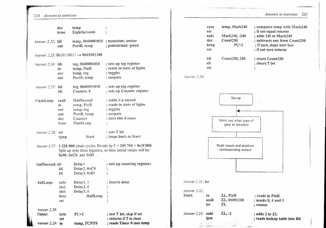
Answers to exercises 225224 Answers to exercises
dec
brne
tempEightSeconds 5
Answer 2.22: ldi
out
temp, ObOOOOlOlO
PortB, temp;motorists: amber
;pedestrians: green
Answer 2.23: Obi 01 1001 1 -> ObOlOOllOO
Answer 2.24: ldi
in
eor
out
tog, ObOOOOlOlO
temp, PinB
temp, tog
PortB, temp
;sets up tog register
;reads in state of lights
;toggles
;outputs
Answer 2.25: ldi
ldi
tog, ObOOOOlOlO
Counter, 8
; sets up tog register
;sets up Counter register
FlashLoop: rcall
in
eor
out
dec
brne
HalfSecond
temp, PinB
temp, tog
PortB, temp
Counter
FlashLoop
;waits M a second
;reads in state of lights
;toggles
;outputs
: does this 8 times
inswer 2.26: set
rjmp Start
;sets T bit
;loops back to Start
Answer 2.27: 1 228 800 clock cycles. Divide by 5 = 245 760 = 0x3C000
Split up over three registers, so their initial values will be:
0x00, OxCO, and 0x03..
HalfSecond: drldi
ldi
Delay 1
Delav2. OxCO
Delav3, 0x03
;sets up counting registers
?
?
-ialfLoop: subi
sbci
sbci
brcc
ret
Delay 1,
1
Delay2, 0
Delav3, 0
HalfLoop
;inserts delay
5
S
9
5
Answer 2.28:
Timer: brts
ret
Answer 2.29: in
PC+2
temp, TCNT0
;test T bit, skip if set
; returns ifT is dear
; reads Timer 0 into temp
cpse temp, Mark240 ; compares temp with Mark240ret
; if not equal returns
subi Mark240, -240; adds 240 to Mark240
dec Count250; subtracts one from Count250
breq PC+2 ; if zero, skips next line
ret; if not zero returns
ldi Count250, 250 ; resets Count250clt ; clears T bit
ret*
Answer 2.30:
Answer 2.31: lsr
Answer 2.32:
Start: in
andi
lsr
ZL, PinB
ZL, ObOOlllO
ZL
; reads in PinB
; masks 0, 4 and 5
; rotates
Answer 2.33: subi
1pmZL, -2
; adds 2 to ZL; reads lookup table into R0
• v* rasas- . *'
226 Answers to exercises
{nswer 2.34: NAND 1110 -> 00110010
NOR 1000 -> 00100000
ENOR 1001 -> 00100001
EOR 01 10 -> 00010010
NOT 1100 -> 00110000
Buffer 0011 -> 00000011
{nswer 2.35:
dw ObOOl 1001 0001 00000 ; NAND and NORdw ObOOlOOOOlOOOlOOlO ; ENOR and EOR
j
dw ObOOl 100000000001 1 : NOT and buffer
; \nswer 2.36:
j
mov temp, RO ;copies R0 to temp
ori temp. Obi 11 10 ;forces bits 1-4 high
out PortB, temp ; outputs result
rjmp Start ; loops back to Start
! nswer 2.37:
64 ms = 256 000 cycles
Divide by 8 = 32 000 decrements - 0x7D00
Delayl initialized to 0x00 and Delay2 initialized to 0x7D
l nswer 2.38:
)oneHi: in Iowerbyte, TCxNTO ;immediately stores TCNTO
cp iowerbyte, temp ;compares with previous value
brsh Divide64 ;jumps to Divide64 if OK
inc upperbvte ; increments higher byte
cpi upperbvte, OxFA ;has it gone too far?
breq TooHigh ;skips to TooHigh if so
nswer 2.39
:
Isr
nswer 2.40:
)ivide64:
nswer 2.41:
ror
Idi
isr
ror
dec
brne
cpi
brne
upperbvte
Iowerbyte
temp, 6
upperbvte
Iowerbyte
tempDivide64+1
upperbyte50
PC+3
;rotates right, bit 7 = 0
;rotates right, bit 7 = carry
;flag
;sets up temp with 6
;divides two-byte word by 2
; does this 6 times
;keeps looping until Finished
;higher byte 0?
; skips next 2 instructions
Answers to exercises 227
cpi Iowerbyte, 0 ;lower byte 0?
breq LowSpeed;jumps to if freq < 1kHz
Answer 2.42: 2 000 000 clock cycles to waste.
14 cycles in loop => 142 857 = 0x022E09
Therefore set up registers with 0x09, 0x2E, and 0x02.
ldi Delayl, 0x09 ; sets ups delay registers
ldi Delay2, 0x2E
ldi Delay3, 0x02
HalfSecond:
rcall Display;calls display for half a second
subi Delayl, 1 ?
sbci Delay2, 0 ?
sbci Delav3, 0 s
brcc HalfSecond
rjmp Start ; loops back to Start
Answer 2.43:
TooHigh: ldi Hundreds, 1
1
; code for a -
ldi Tens. 10;code for a H
ldi Ones, 1 ; code for a I
rjmp Half5econd-3 ; displays for half a second
Answer 2.44:
Display: dec DisplayCounter ; changes display every 50 visits
breq PC+2 ; skips if 50th time
ret;returns
wdr;pats the dog
ldi DisplayCounter, 50 ;resets DisplayCounter
Answer 2.45: inc DisplavNumber ; increments DisplayNumber
cpi DisplayNumber,3; has it reached 3?
brne* PC+2 ; no, so skips
clr DisplavNumber;yes, so clears
Answer 2.46: ldi ZL, 26 ; initializes ZL to R26add ZL, DisplayNumber; points to right digit-
Id temp, Z ; loads value into tempclr ZL
; zeros'ZL to R0add ZL, temp
; adds temp to ZLId temp, Z
; reads Rx into tempsbic PortB, 7 ; tests kHz LED
temp, OblOOOOOOO; if it’s on, keeps it on
- out PortB, temp ; outputs temp to Port B
228 Answers to exercises Answers to exercises 229
Answer 2.47: in temp, PinD ; reads in PinD inc lowerbvte; if not set, adds 1 to answer
lsl temp ; rotates left brne Divide ; overflow?
sbrc temp, 3 ; tests bit 3 of result inc upperbvte;yes, so increments higher byte
ldi temp, ObOOOOOOOl ; resets if gone too far rjmp Divide; keeps looping
out PortD, temp ; outputs result to Port Dret ; returns from the subroutine Answer 2.53:
DoneDividinCM&•
Answer 2.48: real! DigitConvert ; converts answer into digits
LowSpeed: ldi temp, ObOOOOOOOl ; sets TCNTO to count at CK rjmp LowSpeed ; loops back to beginning
out TCCRQ, temp •>
cir Delay2 ; resets delay registers Answer 2.54:
cir Delay3 ; TooSlow: cir temp
cbi PortB, 7 ; clears PB7 to turn on Hz LED out PortD, temp ; turns off Displays
sleep;goes to sleep
Answer 2.49: ldi Counter, 2 ; sets up Counter to 2
cir Delavl ; resets Delayl and TCNTO
I
out TCNTO, Delavl 9 Answers to Chapter 4
j\nswer 2.50: Answer 4.1
:
rjmp Init ; first line executed
i
in store, PinD : stores initial value rjmp Extint ; handles external interrupt
LowLoop: in store2, PinD ; reads in current value rjmp Overflowlnt ; handles TCNTO interrupt
eor store2 , store ;compares initial and current
sbrc store2, 4 ; skips if PD4 unchanged Answer 4.2: ldi temp, ObO 1000000 ; sets bit 6 - enables External
|rjmp Change
;jumps if PD4 changes out GIMSK, temp ; INTO interrupt
cir temp ; selects low level interrupt
Answer 2.51
:
rcall Display ; keeps displays going out MCUCR, temp
ldi temp, ObOOOOOOlO ; enables TCNTO interrupt
mov temp2, Delayl : stores old value out TIMSK, tempin Delavl, TCNTO ; reads in new value
cp Delavl, temp2;compares old and new Answer 4.3:
brsh LowLoop ; loops back of new > old Start: rcall Display;keeps display going
sbic PinD, 1 ; waits for Ready button
inc Delay2;increment higher byte rjmp Start
; keeps looping until pressed
brne LowLoop ;test if zero, loops if isn’t
inc Delay3 ; increments highest byte Answer 4.4: mov temp. Random; multiplies by 5 and.,.
cpi Delays, 0x3E ;too slow? add Random, temp
9
breq TooSlow;yes add Random, temp 9
j
rjmp LowLoop ; no, so loops back add Random, temp9
|
;
add Random, temp ./9
11
inswer 2.52: inc Random, ...adds 1
1 1 divide: sub temp, Delavl ; subtracts result from 400 000
liisbc temp2, Delay2 Answer 4.5: mov CountX, Random
>
II sbc temp3, Delay3 * lsr CountX; divides by 2
^ _
brcs DoneDividing ; if Carry set, finished dividingC— T—
subi CountX,^60; and adds 60
230 Answers to exercises Answers to exercises 231
Answer 4.6
:
Answer 4. 1:
Loopy:
Answer 4.8:
Extint:
Answer 4.9:
Cheat:
Answer 4.10:
Dividel2:
Answer 4.11:
Start:
clr TimeH ; reset timing register sbis ACSR, 5; checks AC result
out IJprtB, TimeH ; turns off display cbi PortD, 3; clears bit 3 if it is low
ldi temp, ObOlOOOOO ;resets INTO interrupt flag sbi PortD, 2
; sets bit 2 in either caseout GIFR 5
ldi temp, ObOOOOOOlO ;resets TCO OVF interrupt flag Answer 4.12: sbis ACSR, 5
; checks AC resultout TIFR cbi PortD, 2
; clears bit 2 if it is low'
sbi PortD, 1;sets bit 1 in either case
sei ; enables interrupts
brid Start ; skips^ut when interrupts sbis ACSR. 5;checks AC result
r-jmp Loopy ;disabled cbi PortD, 1 ; clears bit 1 if it is low
sbi PortD, 0; sets bit 0 in either case
sbis PinD, 0 ; tests LED sbis ACSR, 5; checks AC result
rjmp Cheat cbi PortD, 0; clears bit 0 if it is low
clr temp; stops TCNTO
out TCCRO, temp * Answer 4.1 3: in temp, PortD; reads in Final answer
in TimeL, TCNTO ; reads in TCNTO value swap temp; swap bits 0-3 for 4-7
in temp, TIFR ; test for TCNTO overflow out PortB, temp : outputs resultsbrc temp, 1 rjmp Start .
inc TimeHsubi TimeL, 0xA2 ; subtracts back 0xA2 from Answer 4.14: Obi 110001 1 ADCSRsbci TimeH, 0 ;
total reaction time ObOOOOOOOO -» ADMUXidi temp, ObOOOOOlOl ; restarts TCNTO at CK/1024out TCCRO, temp y Answer 4.15:
Start: cbi ADMUX, 0; selects ADC0 input
sbi ADCSR,ADSC; starts conversion
ldi Hundreds, 10 ; b sbic ADCSR,ADSC; has conversion finished?
ldi
ldi
Tens, 11
Ones, 12
; A;d
rjmp Start+2; no, so keeps waiting
ret Answer 4.16: in Desired,ADCH; reads in 8-bits of answers
com Desired; 5 - answer
clr TimeL;resets result registers
clr TimeH y sbi ADMUX, 0; selects ADCI input
subi temp, 12 ; subtracts 12 from total sbi ADCSR.ADSC; starts conversion on ADCI
sbci tempH, 0? Wait: sbic ADCSR,ADSC
; has conversion finished?brcs DoneDividing
;skips out w7hen there’s a carry rjmp Wait
; no, so keeps waitinginc TimeL
;increment lower byte
brne Dividel2 ;lower byte = 0? Answer 4.11: in Actual,ADCH
; reads in V of actual outputinc TimeH
;yes, so increment higher byte cp Actual, Desired
; compares actual with desiredrjmp Dividel2 ; loop back brio TooLow
; too low ?
cp Desired, Actualy
brio TooHigh; too high?
ldi temp, ObOOOOlOOO; puts initial value in Port D cbi DDRBj 0
; actual ® desired so makes PB0out PortD* temp t ......
,•.
. v rjmp Start ! an innivt ansi 1nnnc fn CfaW
232 Answers to exercises
Answer 4.18:
TooHigh: sbi £>DRB, 0
sbi PortB, 0
rjmp Start
TooLow: sbi DDRB, 0
cbi PortB, 0
rjmp Start
Answer 4,19: clr Address
ldi Data, 0x30
ASCIILoop: out EEAR, Address
out EEDR, Data .
sbi EECR, 1
EEW’ait: sbic EECR, 1
rjmp EEWait
inc Address
inc Data
cpi Data, 0x3A
brne PC+2ldi Data, 0x41
cpi Data, 0x47
brne ASCIILoop
;makes PBO and output
;makes PBO 5V
; loops back to Start
;makes PBO an output
;makes PBO 0V
;loops back to Start
;first address is 0x00
;ASCII for “0” is 0x30
;initiates write
;waits for write to finish
; loops until EECR, 1 is cleared
;selects next address
;selects next ASCII code
; finished doing numbers?
; skips if not finished
; ASCII for “A” is 0x41
;finished completely?
; yes, finished
Answer 4.20: ObOOOOllOl ^ TCCR1B
ObOlOOOOOO -4 TIMSKOxOF -4 OCR1AH0x42 —^ OCR1AL
Answer 4.21:
ToggleOut: in temp, PortB
com temp
out PortB, temp
reti
Answer 4.22:
ChangeNote: dec Length
breq PC+2reti
Rest: in temp,TIFRcKrc tomn 1
;T/Cl prescaled at CK/1024
;reset T/Cl on compare match
;enables output compare int.
;4MHz/ 1024 = 3906Hz
;3906 = 0xF42
;reads in Port B
;inverts bits
; outputs to Port B
;returns
;skips on when enough time
;has passed
;waits until T/C0 overflow
: interrupt flag
Answers to exercises 233[
rjmp Rest ;
ldi temp, ObOOOOOOlO ;resets interrupt flag
out TIFR, temp;
Answer 4.23:
ReadJEEPROM:out EEARL, address
;select address
sbi EECR, 0 ; initiate read
in ZL, EEDR ;reads EEPROM
andi ZL, ObOOOOl 111 ; masks higher nibble
cpi ZL, OxOC ; compares with OxCbreq Reset ; repeats melody if equal
brio PC+2 ; is ZL < OxCldi ZL, 0x00 ; if it is selects a (0x0)
Answer 4.24: Isl ZL ; multiplies ZL by two
subi ZL, -0x26 ; adds 26 to point to table
1pm ; reads table
mov NoteL, R0 ; stores lower byte
inc ZL ; moves to next address
1pm ; reads table
mov NoteH, R0 ; stores higher byte
Answer 4.25: in temp, EEDR ; reads in the byte
swap temp; swaps nibbles
andi temp, ObOOOOOOll;selects correct bits
GetOctave: breq GetLength ; skips if 0
Isr NoteH;rotates higher byte
ror NoteL;rotates lower byte with carry
dec temp;repeats for each octave
rjmp GetOctave9
Answer 4.26 :
GetLength: out OCR1AH, NoteH;stores note values in
out OCR1AL, NoteL;output compare registers
in temp, EEDR ; reads in EEPROM again
andi temp, ObllOOOOOO; masks' bits
swap temp; swaps nibbles
Isr temp; rotates once
subi temp, -2;adds two
mov Length, temp ; moves into Lengthreti ^ .
.
; 'returns
Answers to exercises
Answers to Chapter 5
Answer 5.1:
Parity:
Counter, 8
parityreg
temp
PC+2parityreg
Counter, 8
Parity
;sets up counter with 8
presets register
;rotates temp to the right
;does this 8 times
Bit 0 of parityreg is now a parity bit for temp.
Answer 5.2:
Change:
Answer 5.3: subi
lpm
out
Answer 5.4: Idi
out
clr
out
reti
ZL, UDR ; reads data
ZL, 0x61 ;subtracts 0x61
ZL, 26 ; if ZL is more than 25
PC+2 ;makes ZL = 26
ZL, 26 ;
ZL ; multiples ZL by 2
ZL, -27 ; adds 27, points to higher byte
;reads higher byte
OCR1AH, R0 : stores in OCR1AHZL ;
points to lower byte
; reads lower byte
OCR1AL, R0 ;stores in OCR1AL
ZL, -60 ;points to second lookup table
;reads table
PortB, R0 ;displays result
temp, R0 ; copies R0 to temp
temp, ObOOOOlOOO ;masks all but bit 3
PortD, temp ; copies to PortD to set # LED
temp, ObOlOOOOOO ; OC1 toggles with each Output
TCCR1A, temp ;Compare interrupt
temp ; resets TCNTOTCNTO ;
Answer 5.5:
EndNote: clr
out
iiltoiA,,:-” reti
temp
TCCR1A, temp;disconnects OC1 pin from
; OC interrupt
Answers to exercises 235
Answer 5.6:
.macro skeq ; calls this macro skeq
breq PC+29
.endmacro
Answer 5. 7:
.macro HiVVait; calls this macro HiWait
sbis @0, @1 ;tests input
rjmp PC-1 ; keeps looping until input is :
.endmacro
Answer 5.8:
Display: inc DisplayNumber ; selects next display
cpi DisplayNumber,
4
; gone too far?
brnePC'+2
clr DisplayNumber;yes, so resets to first
ldi ZL, 21 ; zeros ZL to R21
add ZL. DisplayNumber ; adds display numberId temp, Z : reads value
out PortB, temp ; outputs temp to Port B
in temp, PortD ; reads in current value
isi temp; moves to next display
sbrc temp, 7;gone too far?
ldi temp, ObOOOOlOOO ; resets to first display
out PortD, temp;outputs result
reti; returns enabling interrupts
Index
.asm, 24
.cseg, 117
.db, 71, 117
.def. 20
.device, 18, 20
.dw, 70, 71, 124
.endmacro, 144
asr, 5
1
assemble, 8, 13, 20, 25
assembly source, 24
AVR Studio, 25, 26, 30
baud rate, 130-333
bclr, 72
.equ. 20
.eseg, 1 17
.exit, 23
.include, 20
.list, 20
.macro, 144
.nolist, 20
.org. 1 17. 124
ACSR. 105. 106
adc, 76
ADC (10-bit^ 10ADC (4-bit), 106
ADC clock, 110,111
ADC interrupt ffag, 1 10
ADCH, 109. Ill
ADCL, 109, 111
ADCSR, 109. 11®
add 76
addition (binary). 6, 74
address (byte). 65L 124
address (word), 124
binary, 3-8
bit, 4, 5
bid, 76
branching table, 94
brbc, 37
brbs. 37
brcc, 52
breq, 37
brne. 37
brtc, 62
bus. 62
bset, 72
bst, 76
Buffer. 66
button bounce. 42
byte address, 69, 124
call. 145
carry, 5, 73
carry flag, 51, 53, 73
cbi, 25, 31
chaser, 47
adiw, 94
ADMUX, 109-112
analogue compai»r, 97, 105
analogue to digital converter, 106
and, 76
AND, 65
andi, 69
arithmetic shifty 51
ASCII, 117, 134,135, 146, 167
clock cycles, 54
clock frequency, 1 8, 1
clr, 22 y
com, 62'
comments, 17,1
8
common anode, 35
common cathode, 35
compare, 77
comparing, 37
238 Index
counter, 39, 41, 42, 45, 47
cp, 37
cpc, 77
cpi, 39, 47
cpse, 76
CPU model, 8
DAC, 112, 113, 127
DDRB, 21
DDRD, 21
Idebouncing, 57
Sdec, 46, 49, 54
decimal, 3—7
:declarations, 20
: defensive programming, 121
development board, j 0, 3
1
differential amplifier, 1 1
1
|digital to analogue converter, 1 12,
|113,127
I directive, 18, 20, 21, 70, 117, 144
1 dividing, 80, 88
,!
1 EEAR, 116
1 EECR, 116
ilEEDR, 116
I EEPROM, 8, 116, 117, 122, 139
||emulating, 27
IfENOR, 66
If eor, 64, 86
|| exclusive OR, 63, 64, 86
li external interrupt, 97, 98
I flag, 73, 98
If flash, 8
|||flowchart, 8, 10, 12
\ || framing error, 131
I
frequency conter, 77
full duplex, 138
GIFR, 99
GIMSK, 98
half carry flag, 73
half duplex, 138
handshaking, 134
HC (high speed CMOS), 30
hexadecimal, 3-7, 166
HyperTerminal, 133,134
I/O pins, 8-10, 14, 16, 21
I/O registers, 13, 15, 21, 22, 91
icall, 93
ICE, 27
ICP, 119
ICR1H, L, 118, 119
idle mode, 75
ijmp, 94
in circuit emulator, 27
inc, 47
inclusive OR, 63, 64, 71
indirect addressing, 34-36
indirect jump, 93, 94
input capture, 1 19
inputs, 8—10, 16, 21
instructions, 2, 17
INTO, 97, 98
interrupt enable, 73, 98, 103
interrupt handling routine, 98
interrupt vector table, 97, 121
interrupts, 97
invert, 63
jmp, 145
JTAG interface, 145, 151
labels, 17
Id, 38, 91, 93
ldd, 93
ldi, 22
Ids, 93
linear congruential method, 102
loading, 38, 91, 93
logic 0, 8
logic 1, 8
logic operation, 63-66
logical shift, 51
lookup file, 20
lookup table, 36
Index 239
1pm, 39, 68, 71, 124 PIC 2, 3
lsb, 4, 5 PinB, 15, 27
lsl, 51, 124 PinD, 15, 16, 33
lsr, 5
1
pop, 94
PortB, 15 16, 25,27macros, 144 PortB, 39mark/space ratio, 127 PortD, 15, 16, 26
marker, 45 ports, 15, 16, 21
masking, 65, 69, 71 powerdown mode, 75
master/slave, 138 prescaling, 141-143
MCUCR, 76, 98 program counter, 54, 98
MegaAVR, 145 program memory, 8, 55, 69
microcontroller, 1, 7, 8 programming, 30mov, 50 pseudo-surround sound, 1 15
msb, 4, 5 pullups, 2
1
mul, 145 push, 55, 94
multiply, 124, 144, 145
music, 122
PWM, 127, 128, 141, 143
RAM, 8,91,92NAND, 66 random numbers, 102
neg, 76
negative (binary), 6, 7, 76
negative flag, 73
nibble, 5, 7^74noise canceller (input capture), 1 19,
120
nop, 76, 81, 121,144
NOR, 66
NOT, 66
number systems, 3-7
rcall, 56
RCEN, 3
1
reaction tester, 99
registers, 13, 91
registers (I/O), 13, 15, 21, 22, 91
registers (working), 13, 14, 91
reset, 27, 75
ret, 56
reti, 98, 121
RISC, 8
OC1, 127
rjmp, 21, 25, 33, 54
rol, 51
OCR 1 AH, L, 118, 121, 128
one’s complement, 7, 63
ori, 71, 76
oscillator, 18
out, 22, 33
output compare, 12
1
outputs, 8-10, 16, 21
palindrome, 95
parity bit, 129, 130
parsing, 96
PCK, 141
ror, 5
1
rotate, 5 1 , 69, 7 1 , 80
RS232, 134, 136
RXD, 130-133
sbc, 76
sbci, 54
sbi, 17,25,31
sbic, 32, 29, 47sbis, 32, 33, 39
sbiw, 94
sei, 103
.40 index
er, 22
Serial peripheral interface, 138, 139
erial port, 133, 134, 136
et, 64
;even segment display, 34-39, 57,
77
5FIOR, 143
diift register, 130, 138
;ign bit, 7, 73
.implex, 138
emulating, 26
deep, 75-77
SPCR, 139, 140
SPDR, 139
Special Function I/O .egister, 143
speedometer, 120
SPH, 92
SPI, 138, 139
SPIER 31
SPL, 92
SPSR, 139
SRAM, 8, 91, 92
srbc, 77
srbs, 77
SREG, 72, 73
st, 36,91
stack, 55, 92, 94
stack pointer, 92
start bit, 1 30
Status register, 72, 73
std, 93
step into, 26
step out, 57
step over, 57
STK500, 31, 133
stm, 145
stop bit, 1 30
storing, 36, 91
strobing, 9, 10, 77
sts, 93
sub, 76
subi, 46, 54
! _subroutines, 55
swap, 71
synchronous, 138
T bit, 73, 76
TCCR0, 45
TCCR1, 142
TCCR1A, 129
TCCR1B, 119
TCNT0, 44-53
TCNT1B, 117, 118, 128
TCNT1L, 117, 118, 128
TEMP, 118
template, 18, 19
temporary bit, 73, 76
testing, 26, 151
T1FR, 99
timer overflow, 81, 97, 103
timer/counter 1, 117, 118, 121, 128,
141
timing, 44-59
T1MSK, 98, 120, 121
Tiny 15, 111, 141
TinyAVR, 67, 111, 141
trace into, 26
truth table, 63-65
two’s complement, 6, 7, 76
two’s complement flag, 73
TXD, 130, 133
UART, 129-132, 151
UBRR, 131
UCR, 131, 132
UDR, 131
USR, 131, 133
watchdog timer, 74, 77
wdr, 74
wdtcr, 74, 75
word, 13, 14
word address, 69, 124
working registers, 13, 14, 91
writing, 12
XOR, 63, 64, 86
XTAL1/2, 29
Y, 92
Z, 13, 14, 36—38, 68zero flag, 37, 73ZH, 13, 14, 36ZL, 13, 14,36, 37
;
'


![Uvodna riječ [Introductory word.]](https://static.fdokumen.com/doc/165x107/63331824b6829c19b80c4113/uvodna-rijec-introductory-word.jpg)