AUTONOMOUS_ROBOT
Transcript of AUTONOMOUS_ROBOT

FROM:
Engr Rana Muhammad [email protected]://www.facebook.com/EngnrShakeelplz like my page:https://www.facebook.com/Electrical4Electronics
For MORE PROJECTS:http://electro-technolgy.blogspot.com
AUTONOMOUS ROBOT
Abstract
Now-a-days, Automated systems have less manual
operations, flexibility, reliability and accurate. Due to
this demand every field prefers automated control systems.
Especially in the field of electronics automated systems are
giving good performance. In the present scenario of war
situations, unmanned systems plays very important role to
minimize human losses. So this robot is very useful to do
operations like obstacle detection.
This project aims at designing and executing the
obstacle detection and avoidance robot. A robot obstacle

detection system including a robot housing which navigates
with respect to a surface and a sensor subsystem having a
defined relationship with respect to the housing and aimed
at the surface for detecting the surface. The ultrasonic
sensor is a pair sensors has a receiver and a transmitter
sensor. The transmitter sends the ultrasonic waves, and if
the receiver senses any of the transmitted signal it
indicates the presence of an obstacle. If the receiver
doesn’t sense any signal it indicates the absence of
obstacle. If any obstacle is detected the directions of the
robot will be automatically changed.
This robot is fitted with motors. A micro controller is
used to control all operations. According to the motor
operations the robot will operate as specified in program.
However, the microcontroller being used for the
project has latched outputs and as such one does not have to
keep the buttons on remote control passed for more than a
few milliseconds. The working prototype of the land rover
including remote is designed using micro controllers at both
ends with appropriate code written in "C" language.
The programming language used for developing the
software to the microcontroller is Embedded/Assembly. The
KEIL cross compiler is used to edit, compile and debug this
program. Micro Flash programmer is used for burning the

developed code on Keil in to the microcontroller Chip. Here
in our application we are using AT89C51 microcontroller
which is Flash Programmable IC.AT represents the Atmel
Corporation represents CMOS technology is used for designing
the IC. This IC is one of the versions of 8051.

INDEX
1. INTRODUCTION
OBJECTIVE OF THE PROJECT
BLOCK DIAGRAM
2. DESCRIPTION OF THE PROJECT
BLOCK DIAGRAM DESCRIPTION
SCHEMATIC
3. HARDWARE DESCRIPTION
MICROCONTROLL
L293D
DC MOTOR
ULTRASONIC SENSOR
4. SOFTWARE DESCRIPTION
KEIL C
CODE
5. CONCLUSION
6. BIBLIOGRAPHY

INTRODUCTION
Objective:
The main aim of this project is to develop a
robot, which automatically controls the robot using 8051
Micro controller.
BLOCK DIAGRAM :
MCU
ULTRASONICTRANSMITTER
DC MOTOR
L293D
BATTERY

Description: This application is in the area of embedded systems.
An embedded system is some combination of computer
hardware and software, either fixed in capability or
programmable, that is specifically designed for a particular
function
Since the embedded system is dedicated to specific tasks,
design engineers can optimize it reducing the size and cost of
the product and increasing the reliability and performance.
Embedded systems are controlled by one or more main processing
cores that is typically either a microcontroller or a digital
ULTRASONICRECEIVER
signal processor (DSP). Embedded systems control many devices
in common use today.
The Keil C51 C Compiler for the 8051 microcontroller is
the most popular 8051 C compiler in the world. It provides more
features than any other 8051 C compiler available today. The
C51 Compiler allows you to write 8051 microcontroller
applications in C that, once compiled, have the efficiency and
speed of assembly language. Language extensions in the C51
Compiler give you full access to all resources of the 8051.
The C51 Compiler translates C source files into
relocatable object modules which contain full symbolic
information for debugging with the µVision Debugger or an in-
circuit emulator. In addition to the object file, the compiler
generates a listing file which may optionally include symbol
table and cross reference information.
Embedded C is an extension for the programming language C
to support embedded processors, enabling portable and efficient
application programming for embedded systems
The AT89C51 is a low-power, high-performance CMOS 8-bit
microcomputer with 4K bytes of Flash programmable and erasable
read only memory (EPROM). The device is manufactured using
Atmel’s high-density nonvolatile memory technology and is
compatible with the industry-standard MCS-51 instruction set

and pinout. The on-chip Flash allows the program memory to be
reprogrammed in-system or by a conventional nonvolatile memory
programmer. By combining a versatile 8-bit CPU with Flash on a
monolithic chip, the Atmel AT89C51 is a powerful microcomputer
which provides a highly-flexible and cost-effective solution to
many embedded control applications.
This project aims at designing and executing the fire
sensing, alcohol, bomb and obstacle detection and avoidance
robot. A robot obstacle detection system including a robot
housing which navigates with respect to a surface and a
sensor subsystem having a defined relationship with respect
to the housing and aimed at the surface for detecting the
surface. The ultrasonic sensor is a pair sensors has a
receiver and a transmitter sensor. The transmitter sends the
ultrasonic waves, and if the receiver senses any of the
transmitted signal it indicates the presence of an obstacle.
If the receiver doesn’t sense any signal it indicates the
absence of obstacle. If any obstacle is detected the
directions of the robot will be automatically changed.
This robot is fitted with motors. A micro controller is
used to control all operations. According to the motor
operations the robot will operate as specified in program.

SCHEMATIC:

XTAL218
XTAL119
ALE30EA31PSEN29
RST9
P0.0/AD0 39P0.1/AD1 38P0.2/AD2 37P0.3/AD3 36P0.4/AD4 35P0.5/AD5 34P0.6/AD6 33P0.7/AD7 32
P1.01P1.12P1.23P1.34P1.45P1.56P1.67P1.78
P3.0/RXD 10P3.1/TXD 11P3.2/INT0 12P3.3/INT1 13P3.4/T0 14
P3.7/RD 17P3.6/W R 16P3.5/T1 15
P2.7/A15 28
P2.0/A8 21P2.1/A9 22P2.2/A10 23P2.3/A11 24P2.4/A12 25P2.5/A13 26P2.6/A14 27
U1
AT89C51
IN12 OUT1 3OUT2 6
OUT3 11OUT4 14
IN27
IN310IN415
EN11
EN29
VS
8
VSS
16
GND GND
U2
L293D
ULTRASONIC TRANSM ITTER
ULTRASONIC RECEIVER
8051 Micro controller:

The first microprocessor introduced in 1981/1971,
was made possible by high levels of integration of digital
circuits. Continued integration of peripherals and memory on
the same integrated circuit as the microprocessor core led
to the creation of micro controllers. A micro controller is
an integrated circuit composed of a CPU, various peripheral
devices, and typically memory, all in one chip. Using one
chip that contains all the necessary functions in place of a
microprocessor and multiple peripheral chips has reduced the
size and the power consumption of control oriented
applications. A micro controller is different from a
microprocessor both in hardware and software. In hardware it
includes peripherals such as I/O, memory, and analog and
digital interface. Micro controllers are more suited for
small applications with specific control functions requiring
specialized peripherals and interfaces.
They are designed for process control and are required
to interface to the real world processes. Many of the
peripheral devices integrated on a micro controller are for
that specific purpose. Analog to digital converters perform
the task of converting an analog signal to digital for use
by the CPU, and digital to analog converters perform the
task of converting digital data into analog value and
waveforms to control analog functions. In addition to the
analog interface, micro controllers contain peripheral
devices that enable them to communicate to other digital

components within a system or to monitor and control digital
functions. Communication interfaces, digital I/O and
interrupt controllers fall into this category of peripheral
devices. Other peripheral devices often included on the same
chip include clocks and timers.
In terms of the software, micro controllers have
a more compact set of instructions with commands more suited
to process control such as input and output from. Single bit
operations such as set and reset, bit-wise logical functions
or branching instructions that depend on a single bit are
commonly available as part of the instruction set to allow
for reading input switch status or on/off control of an
external event. Since in a given application the micro
controller is programmed for one task, it only has one
control program. In a microprocessor based system various
programs are stored in a mass storage device and then loaded
into the RAM for execution. In contrast the micro controller
program is typically stored in a ROM or PROM and RAM is used
for temporary storage of data.
Compared with discrete implementation of a system, the
micro controller based approach provides shorter system
development time, reduced implementation cost, lower power
consumption, and higher reliability. The only drawback,
which is often not important, is the lower speed of
execution. For example, for a micro controller system to

perform a logical operation, several clock cycles are needed
to read the inputs, perform the function and output the
results. The same operation when implemented with discrete
components will provide the results as soon as the signals
have propagated through the logic gates.
Micro-controllers are used in a variety of
process control applications, replacing complex digital
circuits and sometimes-analog functions while providing more
flexibility due to their programmability. Portable
electronic devices such as personal audio devices (CD
players, MP3 players), mobile telephones, digital cameras
and video camcorders rely heavily on the reduced size and
low power consumption of micro controller based electronics.
These features are crucial to applications like implantable
medical devices such as pacemakers, or personal medical
monitoring devices like glucometers (electronic devices used
for the measurement of blood glucose). In other applications
such as appliances, home audio and video, automotive, power
management, and temperature control, using a micro
controller results in reduced board level circuit complexity
and consequently reduced cost. With the growing number of
applications using micro controllers, it is not surprising
that there are such a wide variety of these components. In
addition to those commonly available, many manufacturers
custom-design a micro controller to suit a specific
application.

Architecture
Architecturally all micro controllers
share certain features. They all contain a CPU, memory and
I/O on the same chip. Another common feature is the
interrupt handling capability. What sets them apart from one
another is the choice of CPU, the structure of memory, and
choice of peripheral devices, I/O and interrupts handling
hardware. The major distinguishing architectural
characteristic of micro controllers is the word size. Micro-
controllers are available in 4, 8, 16, or 32 bit wide words.
The width of the data path impacts several features of the
micro controller. The complexity of the instruction set
(number of available instructions and addressing modes),
program efficiency (code generation and storage space),
execution speed, as well as chip implementation and
interfacing complexity are all influenced by the width of
the data path.
For simple control tasks 4-bit, and for a vast number
of control and measurement applications 8-bit micro
controllers would be sufficient. For higher precision and
speed applications like speech and video processing, or
complex instrumentation, 16-bit and 32-bit micro controllers
are more appropriate.

Another distinction between micro controllers is the
instruction set. Micro-controllers with complex instruction
set (CISC) provide capability to perform complex
computations rapidly. The extensive set of instructions,
allow complex operations to be performed with few
instructions. On the other hand reduced instruction set
computers (RISC) decrease program execution time by having
fewer less complex instructions. Fewer available
instructions results in faster execution due to smaller size
of the op-code and less decoding time needed for each
instruction. The trade-off depends on the complexity of
operations needed for a specific application. In simple
control applications a RISC based micro controller is more
suitable because of its lower overhead for each instruction.
In more complex applications, the availability of a more
diverse instruction set results in a more efficient and
faster executing code because fewer instructions are needed
to accomplish a complicated task. For micro controller
applications the instruction set should include common
computational instructions plus instructions optimized for
the specific application at hand.
Just as in microprocessors, micro controllers are also
differentiated according to their memory structure. Von
Neumann architecture maps the data and program to same
memory address space. In the Harvard architecture the
instructions are stored in a separate memory space than that

used for data storage. Another memory related architectural
characteristic of a processor is the addressing scheme. In
linear addressing there is a one to one correspondence
between an address and a memory location. So with an 8-bit
address register, 28 distinct address locations can be
accessed. In segmented addressing a separate register is
used to point to a segment in memory, and the address
register is used to point to an offset from that segment’s
start point. This way if all of the program or data are in
the same segment, in order to access them, only the address
register need to be used and the segment register can remain
pointing to the start point of that segment.
Widely used group of micro controllers is Intel’s
MCS51 family. These micro controllers are also 8-bit
processors, but with a separate 64Kbyte of data and 64Kbyte
of program memory space. As implied by this statement,
devices in the MCS51 utilize Harvard architecture. All of
I/O addresses as well as CPU registers and various
peripheral devices’ registers are mapped in the same space
as the data. The 8051, which is one of the options in this
family, has 5 interrupt sources, 2 external, two timer
interrupts and one serial port interrupt. Interrupt priority
is resolved through a priority scheme and ranking in the
polling sequence. The priority scheme allows each interrupt
to be programmed to one of two priority levels. Furthermore
if two interrupts with the same priority occur

simultaneously, they are serviced based on their rank in the
polling sequence. Other manufacturers such as AMD, Dallas
Semiconductor, Fujitsu and Philips also supply micro
controllers in the MCS51 family.
BLOCK DIAGRAM:

Fig Block Diagram of AT89C51 Microcontroller
Dallas Semiconductor’s DC87C550 provides increased
performance over Intel’s 8051 while maintaining instruction
set compatibility. Many instructions that execute in 12 CPU
clock cycles in an 8051, will execute in only 4 clocks for

the DC87C550 therefore resulting in increased execution
speeds of up to three times. Additionally, the DC87C550 has
a power management mode that allows slowing of the processor
in order to reduce power consumption. This mode can be
utilized in battery operated or otherwise low power
applications. The architecture of the instruction set varies
greatly from one micro controller to another. The choices
made in designing the instruction set impact program memory
space usage, code execution speed, and ease of programming.
PIN CONFIGURATION:

Fig Pin Configuration of AT89C51
Pin Description:
VCC:
Supply voltage.
GND:
Ground.
Port 0:
Port 0 is an 8-bit open-drain bi-directional I/O port. As an
output port, each pin can sink eight TTL inputs. When 1’s
are written to port 0 pins, the pins can be used as high
impedance inputs. Port 0 may also be configured to be the
multiplexed low order address/data bus during accesses to
external program and data memory. In this mode P0 has
internal pull-ups. Port 0 also receives the code bytes
during Flash programming, and outputs the code bytes during
program verification. External pull-ups are required during
program verification.
Port 1:

Port 1 is an 8-bit bi-directional I/O port with internal
pull-ups. The Port 1 output buffers can sink/source four TTL
inputs. When 1s are written to Port 1 pins they are pulled
high by the internal pull-ups and can be used as inputs. As
inputs, Port 1 pins that are externally being pulled low
will source current (IIL) because of the internal pull-ups.
Port 1 also receives the low-order address bytes during
Flash programming and verification.
Port 2:
Port 2 is an 8-bit bi-directional I/O port with internal
pull-ups. The Port 2 output buffers can sink/source four TTL
inputs. When 1s are written to Port 2 pins they are pulled
high by the internal pull-ups and can be used as inputs. As
inputs, Port 2 pins that are externally being pulled low
will source current (IIL) because of the internal pull-ups.
Port 2 emits the high-order address byte during fetches from
external program memory and during accesses to external data
memories that use 16-bit addresses (MOVX @DPTR). In this
application, it uses strong internal pull-ups when emitting
1s. During accesses to external data memories that use 8-bit
addresses (MOVX @ RI), Port 2 emits the contents of the P2
Special Function Register. Port 2 also receives the high-
order address bits and some control signals during Flash
programming and verification.
Port 3:

Port 3 is an 8-bit bi-directional I/O port with internal
pullups.The Port 3 output buffers can sink/source four TTL
inputs. When 1s are written to Port 3 pins they are pulled
high by the internal pull-ups and can be used as inputs. As
inputs, Port 3 pins that are externally being pulled low
will source current (IIL) because of the pull-ups.
Port 3 also serves the functions of various special features
of the AT89C51 as listed below:
Port 3 also receives some control signals for Flash
programming and verification
Tab Port pins and their alternate functions
RST:
Reset input. A high on this pin for two machine cycles while
the oscillator is running resets the device.
ALE/PROG:

Address Latch Enable output pulse for latching the low byte
of the address during accesses to external memory. This pin
is also the program pulse input (PROG) during Flash
programming. In normal operation ALE is emitted at a
constant rate of 1/6the oscillator frequency, and may be
used for external timing or clocking purposes. Note,
however, that one ALE pulse is skipped during each access to
external Data Memory.
If desired, ALE operation can be disabled by setting bit 0
of SFR location 8EH. With the bit set, ALE is active only
during a MOVX or MOVC instruction. Otherwise, the pin is
weakly pulled high. Setting the ALE-disable bit has no
effect if the microcontroller is in external execution mode.
PSEN:
Program Store Enable is the read strobe to external program
memory. When the AT89C51 is executing code from external
program memory, PSEN is activated twice each machine cycle,
except that two PSEN activations are skipped during each
access to external data memory.
EA/VPP:
External Access Enable. EA must be strapped to GND in order
to enable the device to fetch code from external program
memory locations starting at 0000H up to FFFFH.
Note, however, that if lock bit 1 is programmed, EA will be
internally latched on reset.

EA should be strapped to VCC for internal program
executions. This pin also receives the 12-volt programming
enable voltage (VPP) during Flash programming, for parts
that require 12-volt VPP.
XTAL1:
Input to the inverting oscillator amplifier and input to the
internal clock operating circuit.
XTAL2:
Output from the inverting oscillator amplifier.
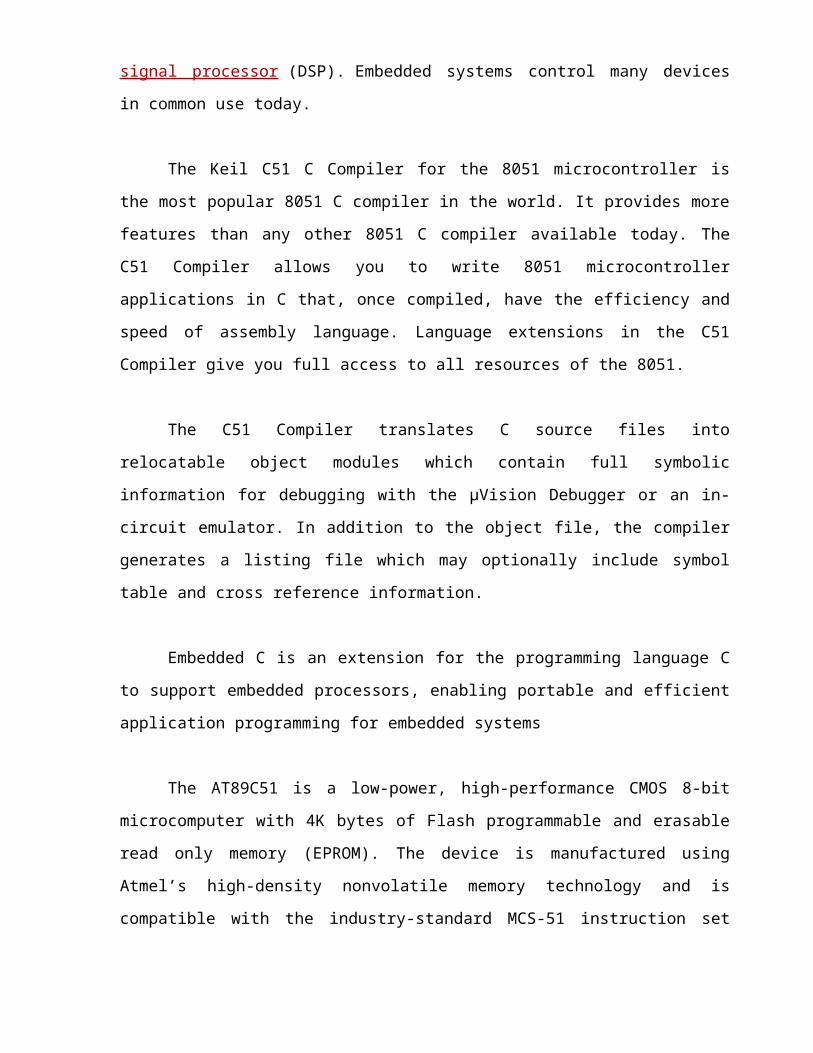
Oscillator Characteristics:
XTAL1 and XTAL2 are the input and output, respectively, of
an inverting amplifier which can be configured for use as an
on-chip oscillator, as shown in Figs 6.2.3. Either a quartz
crystal or ceramic resonator may be used. To drive the
device from an external clock source, XTAL2 should be left
unconnected while XTAL1 is driven as shown in Figure
6.2.4.There are no requirements on the duty cycle of the
external clock signal, since the input to the internal
clocking circuitry is through a divide-by-two flip-flop, but
minimum and maximum voltage high and low time specifications
must be observed.
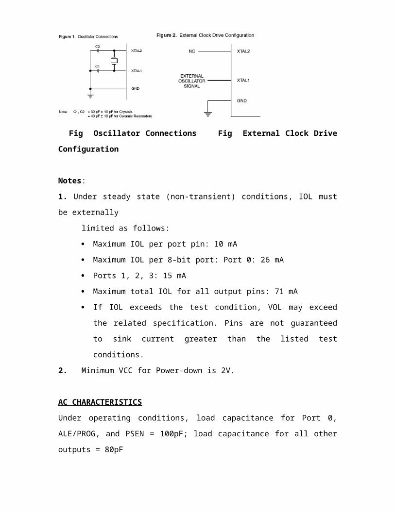
Fig Oscillator Connections Fig External Clock Drive
Configuration
Notes:
1. Under steady state (non-transient) conditions, IOL must
be externally
limited as follows:
Maximum IOL per port pin: 10 mA
Maximum IOL per 8-bit port: Port 0: 26 mA
Ports 1, 2, 3: 15 mA
Maximum total IOL for all output pins: 71 mA
If IOL exceeds the test condition, VOL may exceed
the related specification. Pins are not guaranteed
to sink current greater than the listed test
conditions.
2. Minimum VCC for Power-down is 2V.
AC CHARACTERISTICS
Under operating conditions, load capacitance for Port 0,
ALE/PROG, and PSEN = 100pF; load capacitance for all other
outputs = 80pF

Hardware
There are a variety of peripheral devices that are
often integrated on a micro controller chip. Many of these
peripheral devices are the same as those that may be
included in a microprocessor while those that make a micro
controller distinguishable from a microprocessor are the
ones that deal with external interface and communication.
Here is a brief description of the hardware components of a
micro controller:
1. Interrupt Handlers
An interrupt is an event (internal or
external to the chip) that occurs asynchronously with other
functions and requires immediate response from the micro
controller. Such events can be detected if the micro
controller constantly or periodically monitors their status.
But such polling techniques could slow the operation of
other functions. To detect and prioritize interrupts,
interrupt handling hardware is often included on the micro
controller chip. Interrupt handlers usually provide multiple
interrupt inputs, with different levels of priority and the
means to mask certain interrupts. An example of interrupts
is power failure in a hand held thermometer. Should the
battery voltage drop below acceptable limits at any time,
the device should inform the user of the condition and

possibly perform preventive measures before returning
control to the interrupted program.
2. I/O ports
I/O ports provide means of digital data
transfer to and from the micro controller. I/O ports are
usually configured as a parallel interface where digital
data can be simultaneously written to or read from a port
address. In micro controller applications it is often
possible to use the I/O ports with bit wise instructions.
I/O ports can be used for crude user interface functions
such as reading of switch settings or displaying some
results using LED’s. It is also possible to use I/O ports
for more sophisticated interface options. An I2C interface,
which is a serial communications protocol, can be emulated
using two bits of an I/O port.
3. Digital to Analog Converters (DAC)
DAC’s provide continuous time output
capability by converting a digital word to a proportional
voltage or current. Different DAC architectures provide
trade-offs in design complexity, resolution, accuracy, and
speed. Creating the audio waveforms from the data in a high-
end digital audio player requires a high resolution DAC with
moderate conversion rate, while creating the waveforms to
drive an analog display requires lower resolution at higher
conversion rate.

4. Analog to Digital Converters (ADC)
ADC’s are used to enable the micro
controller to receive continuous time signals representing
physical parameters. Temperature, sound, light intensity,
color, liquid or gas flow, position and speed are all
examples physical parameters that may be used by a micro
controller. These data are first converted to a voltage or
current waveform using appropriate transducers. It is then
the function of the ADC to convert the voltage or current to
digital form for processing by the microprocessor. There are
different types of ADC’s and the choice depends on the
required accuracy, sampling rate and cost.
A) Flash Converters
In a flash ADC multiple analog
comparators are used to evaluate the analog input voltage.
All the bits of the output digital word are evaluated at
once. The only delay in this conversion is that of the
analog comparators and the logic used to encode the digital
word. This is therefore the fastest method of analog to
digital conversion. The resolution is usually limited to 8-
bits because of the large number of comparators needed. High
speed video processing is an application where flash
converters are well suited.
b) Successive Approximation Register (SAR)

In this type of converter, the digital
output is evaluated one-bit at a time starting at the most
significant bit. This type of ADC provides good resolution
(10-12 bits) at relatively fast conversion rate. For a 10-
bit conversion, 10 clock cycles are needed, where the
maximum clock rate depends on the comparator settling and
digital delays in the SAR circuit. The ADC circuit requires
a high speed precise DAC. This is the most commonly used ADC
in micro controller applications.
c) Dual Slope ADC
For high resolution conversions dual
slope converters provide a reasonable tradeoff at the
expense of conversion speed. The conversion of an analog
input to digital is performed by first converting the input
voltage to time, and then measuring time using a clock.
Because of the architecture of dual slope converters, non-
ideal behavior of analog circuits is avoided and high
resolutions (12-16 bits) and accuracies are achievable. This
approach is most useful in applications where precise
measurements of slow signals are needed. Medical
instrumentation and monitoring is an area that fits these
criteria.
d) Over-sampling ADC
Precision analog circuits used in
conventional ADC’s are sometimes difficult to implement in

micro controller integrated circuits because of the highly
noisy environment and process limitations associated with
high levels of integration. The alternative is using over-
sampling converters which can use simple but robust analog
circuits along with fast and complex digital circuits. These
converters sample the data with low resolution at much
higher frequency than what is needed based on Nyquist
theorem and use feedback to improve the effective
resolution. Because of the required over-sampling, the
effective sampling rate is limited. Digitization of voice-
band signals in telecommunication systems is often performed
using over-sampling techniques.
5. Serial Communication Interface
Through the use of serial communication
the micro controller can be used with various system level
peripherals. Here is a brief description of some the serial
communication peripherals commonly integrated on a micro
controller chip.
a SFRs:
The 8051 is a flexible micro controller with a
relatively large number of modes of operations. Your program
may inspect and/or change the operating mode of the 8051 by
manipulating the values of the 8051's Special Function
Registers (SFRs). SFRs are accessed as if they were normal
Internal RAM. The only difference is that Internal RAM is

from address 00h through 7Fh whereas SFR registers exist in
the address range of 80h through FFh. Each SFR has an
address (80h through FFh) and a name. The following chart
provides a graphical presentation of the 8051's SFRs, their
names, and their address.
Tab Chart of 8051 SFRs and their addresses
As we can see, although the address range of 80h through FFh
offer 128 possible addresses, there are only 21 SFRs in a
standard 8051. All other addresses in the SFR range (80h
through FFh) are considered invalid. Writing to or reading
from these registers may produce undefined values or
behavior.
SFR Types
As mentioned in the chart itself, the SFRs that have a
blue background are SFRs related to the I/O ports. The 8051
has four I/O ports of 8 bits, for a total of 32 I/O lines.

Whether a given I/O line is high or low and the value read
from the line are controlled by the SFRs in green. The SFRs
with yellow backgrounds are SFRs which in some way control
the operation or the configuration of some aspect of the
8051.
For example, TCON controls the timers, SCON controls the
serial port. The remaining SFRs, with green backgrounds, are
"other SFRs." These SFRs can be thought of as auxiliary SFRs
in the sense that they don't directly configure the 8051 but
obviously the 8051 cannot operate without them. For example,
once the serial port has been configured using SCON, the
program may read or write to the serial port using the SBUF
register.
SFR Descriptions
This section will endeavor to quickly overview each of the
standard SFRs found in the above SFR chart map. It is not
the intention of this section to fully explain the
functionality of each SFR--this information will be covered
in separate chapters of the tutorial. This section is to
just give you a general idea of what each SFR does.
P0 (Port 0, Address 80h, Bit-Addressable): This is
input/output port 0. Each bit of this SFR corresponds to one
of the pins on the microcontroller. For example, bit 0 of
port 0 is pin P0.0, bit 7 is pin P0.7. Writing a value of 1
to a bit of this SFR will send a high level on the

corresponding I/O pin whereas a value of 0 will bring it to
a low level.
SP (Stack Pointer, Address 81h): This is the stack pointer
of the microcontroller. This SFR indicates where the next
value to be taken from the stack will be read from in
Internal RAM.
If you push a value onto the stack, the value will be
written to the address of SP + 1. That is to say, if SP
holds the value 07h, a PUSH instruction will push the value
onto the stack at address 08h. This SFR is modified by all
instructions which modify the stack, such as PUSH, POP,
LCALL, RET, RETI, and whenever interrupts are provoked by
the microcontroller.
DPL/DPH (Data Pointer Low/High, Addresses 82h/83h): The SFRs
DPL and DPH work together to represent a 16-bit value called
the Data Pointer. The data pointer is used in operations
regarding external RAM and some instructions involving code
memory. Since it is an unsigned two-byte integer value, it
can represent values from 0000h to FFFFh (0 through 65,535
decimal).
PCON (Power Control, Addresses 87h): The Power Control SFR
is used to control the 8051's power control modes. Certain
operation modes of the 8051 allow the 8051 to go into a type
of "sleep" mode which requires much less power.
These modes of operation are controlled through PCON.
Additionally, one of the bits in PCON is used to double the
effective baud rate of the 8051's serial port.
TCON (Timer Control, Addresses 88h, and Bit-Addressable):
The Timer Control SFR is used to configure and modify the
way in which the 8051's two timers operate. This SFR
controls whether each of the two timers is running or
stopped and contains a flag to indicate that each timer has
overflowed. Additionally, some non-timer related bits are
located in the TCON SFR. These bits are used to configure
the way in which the external interrupts are activated and
also contain the external interrupt flags which are set when
an external interrupt has occurred.
TMOD (Timer Mode, Addresses 89h): The Timer Mode SFR is used
to configure the mode of operation of each of the two
timers. Using this SFR your program may configure each timer
to be a 16-bit timer, an 8-bit auto reload timer, a 13-bit
timer, or two separate timers. Additionally, you may
configure the timers to only count when an external pin is
activated or to count "events" that are indicated on an
external pin.

TL0/TH0 (Timer 0 Low/High, Addresses 8Ah/8Bh): These two
SFRs, taken together, represent timer 0. Their exact
behavior depends on how the timer is configured in the TMOD
SFR; however, these timers always count up. What is
configurable is how and when they increment in value.
TL1/TH1 (Timer 1 Low/High, Addresses 8Ch/8Dh): These two
SFRs, taken together, represent timer 1. Their exact
behavior depends on how the timer is configured in the TMOD
SFR; however, these timers always count up. What is
configurable is how and when they increment in value.
P1 (Port 1, Address 90h, Bit-Addressable): This is
input/output port 1. Each bit of this SFR corresponds to one
of the pins on the microcontroller. For example, bit 0 of
port 1 is pin P1.0, bit 7 is pin P1.7. Writing a value of 1
to a bit of this SFR will send a high level on the
corresponding I/O pin whereas a value of 0 will bring it to
a low level.
SCON (Serial Control, Addresses 98h, Bit-Addressable): The
Serial Control SFR is used to configure the behavior of the
8051's on-board serial port. This SFR controls the baud rate
of the serial port, whether the serial port is activated to
receive data, and also contains flags that are set when a
byte is successfully sent or received.

SBUF (Serial Control, Addresses 99h): The Serial Buffer SFR
is used to send and receive data via the on-board serial
port. Any value written to SBUF will be sent out the serial
port's TXD pin. Likewise, any value which the 8051 receives
via the serial port's RXD pin will be delivered to the user
program via SBUF. In other words, SBUF serves as the output
port when written to and as an input port when read from.
P2 (Port 2, Address A0h, Bit-Addressable): This is
input/output port 2. Each bit of this SFR corresponds to one
of the pins on the microcontroller. For example, bit 0 of
port 2 is pin P2.0, bit 7 is pin P2.7. Writing a value of 1
to a bit of this SFR will send a high level on the
corresponding I/O pin whereas a value of 0 will bring it to
a low level.
IE (Interrupt Enable, Addresses A8h): The Interrupt Enable
SFR is used to enable and disable specific interrupts. The
low 7 bits of the SFR are used to enable/disable the
specific interrupts, where as the highest bit is used to
enable or disable ALL interrupts.
Thus, if the high bit of IE is 0 all interrupts are disabled
regardless of whether an individual interrupt is enabled by
setting a lower bit.
P3 (Port 3, Address B0h, Bit-Addressable): This is
input/output port 3. Each bit of this SFR corresponds to one

of the pins on the microcontroller. For example, bit 0 of
port 3 is pin P3.0, bit 7 is pin P3.7. Writing a value of 1
to a bit of this SFR will send a high level on the
corresponding I/O pin whereas a value of 0 will bring it to
a low level.
IP (Interrupt Priority, Addresses B8h, Bit-Addressable): The
Interrupt Priority SFR is used to specify the relative
priority of each interrupt. On the 8051, an interrupt may
either be of low (0) priority or high (1) priority. An
interrupt may only interrupt interrupts of lower priority.
For example, if we configure the 8051 so that all interrupts
are of low priority except the serial interrupt, the serial
interrupt will always be able to interrupt the system, even
if another interrupt is currently executing. However, if a
serial interrupt is executing no other interrupt will be
able to interrupt the serial interrupt routine since the
serial interrupt routine has the highest priority.
PSW (Program Status Word, Addresses D0h, Bit-Addressable):
The Program Status Word is used to store a number of
important bits that are set and cleared by 8051
instructions. The PSW SFR contains the carry flag, the
auxiliary carry flag, the overflow flag, and the parity
flag. Additionally, the PSW register contains the register
bank select flags which are used to select which of the "R"
register banks are currently selected.

ACC (Accumulator, Addresses E0h, Bit-Addressable): The
Accumulator is one of the most used SFRs on the 8051 since
it is involved in so many instructions. The Accumulator
resides as an SFR at E0h, which means the instruction MOV A,
#20h is really the same as MOV E0h,#20h. However, it is a
good idea to use the first method since it only requires two
bytes whereas the second option requires three bytes.
B (B Register, Addresses F0h, Bit-Addressable): The "B"
register is used in two instructions: the multiply and
divide operations. The B register is also commonly used by
programmers as an auxiliary register to temporarily store
values.
Basic Registers
The Accumulator
The Accumulator, as its name suggests, is used as a
general register to accumulate the results of a large
number of instructions. It can hold an 8-bit (1-byte)
value and is the most versatile register the 8051 has due
to the shear number of instructions that make use of the
accumulator. More than half of the 8051’s 255
instructions manipulate or use the accumulator in some
way. For example, if we add the number 10 and 20, the
resulting 30 will be stored in the accumulator.

The "R" registers
The "R" registers are a set of eight registers that are
named R0, R1, etc. up to and including R7. These registers
are used as auxiliary registers in many operations. To
continue with the above example, perhaps you are adding 10
and 20. The original number 10 may be stored in the
Accumulator whereas the value 20 may be store
in, say, register R4. To process the addition you would
execute the command:
ADD A,R4 After executing this instruction the Accumulator
will contain the value 30.
The "R" registers as very important auxiliary, or "helper",
registers. The Accumulator alone would not be very useful if
it were not for these "R" registers. The "R" registers are
also used to temporarily store values.
MOV A, R3; Move the value of R3 into the accumulator
ADD A, R4; Add the value of R4
MOV R5, A; Store the resulting value temporarily in R5
MOV A, R; Move the value of R1 into the accumulator
ADD A,R2 ;Add the value of R2
SUBB A,R5 ;Subtract the value of R5 (which now contains R3 + R4)
In the above example we used R5 to temporarily hold the sum
of R3 and R4. Of course, this isn’t the most efficient way
to calculate (R1+R2) - (R3 +R4) but it does illustrate the
use of the "R" registers as a way to store values
temporarily.
The "B" Register
The "B" register is very similar to the Accumulator in the
sense that it may hold an 8-bit (1-byte) value. The "B"
register is only used by two 8051 instructions: MUL AB and
DIV AB. Thus, if you want to quickly and easily multiply or
divide A by another number, you may store the other number
in "B" and make use of these two instructions.
Aside from the MUL and DIV an instruction, the “B” register
is often used as yet another temporary storage register much
like a ninth "R" register.
The Data Pointer (DPTR)
The Data Pointer (DPTR) is the 8051’s only user-accessible
16-bit (2-byte) register. The Accumulator, "R" registers,
and "B" register are all 1-byte values. DPTR, as the name
suggests, is used to point to data. It is used by a number
of commands which allow the 8051 to access external memory.
When the 8051 accesses external memory it will access
external memory at the address indicated by DPTR. While DPTR
is most often used to point to data in external memory, many
programmers often take advantage of the fact that it’s the
only true 16-bit register available. It is often used to
store 2-byte values which have nothing to do with memory
locations.
The Program Counter (PC)
The Program Counter (PC) is a 2-byte address which tells the
8051 where the next instruction to execute is found in
memory.
When the 8051 is initialized PC always starts at 0000h and
is incremented each time an instruction is executed. It is
important to note that PC isn’t always incremented by one.
Since some instructions require 2 or 3 bytes the PC will be
incremented by 2 or 3 in these cases. The Program Counter is
special in that there is no way to directly modify its
value. That is to say, you can’t do something like PC=2430h.
On the other hand, if you execute LJMP 2340h you’ve
effectively accomplished the same thing. It is also
interesting to note that while you may change the value of
PC (by executing a jump instruction, etc.) there is no way
to read the value of PC. That is to say, there is no way to
ask the 8051.
Events that Trigger Interrupts
The 8051 can be configured so that any of the following
events will cause an interrupt:
• Timer 0 Overflow.
• Timer 1 Overflow.
• Reception/Transmission of Serial Character.
• External Event 0.
• External Event 1.
In other words, we can configure the 8051 so that when Timer
0 overflows or when a character is sent/received, the

appropriate interrupt handler routines are called. Obviously
we need to be able to distinguish between various
interrupts and executing different code depending on what
interrupt was triggered. This is accomplished by jumping to
a fixed address when a given interrupt occurs.
Tab Interrupt Handler Address and the Interrupts associated
to them
By consulting the above chart we see that whenever Timer
0 overflows (i.e., the TF0 bit is set), the main program
will be temporarily suspended and control will jump to
00BH. It is assumed that we have code at address 0003H that
handles the situation of Timer 0 overflowing.
Setting up Interrupts
By default at power up, all interrupts are disabled. This
means that even if, for example, the TF0 bit is set, the
8051 will not execute the interrupt. Your program must
specifically tell the 8051 that it wishes to enable
interrupts and specifically which interrupts it wishes to
enable. Your program may enable and disable interrupts by
modifying the IE SFR (A8h):

Tab Setting up Interrupts
For example, to enable Timer 1 Interrupt, you would execute
either:
MOV IE, #08h || SETB ET1
Both of the above instructions set bit 3 of IE, thus
enabling Timer 1 Interrupt. Once Timer 1 Interrupt is
enabled, whenever the TF1 bit is set, the 8051 will
automatically put "on hold" the main program and execute the
Timer 1 Interrupt Handler at address 001Bh. However,
before Timer 1 Interrupt (or any other interrupt) is truly
enabled, you must also set bit 7 of IE. Bit 7, the Global
Interrupt Enable/Disable, enables or disables all interrupts
simultaneously. That is to say, if bit 7 is cleared then no
interrupts ill occur, even if all the other bits of IE are
set. Setting bit 7 will enable all the interrupts that have
been selected by setting other bits in IE. This is useful in
program execution if you have time-critical code that needs
to execute.
In this case, you may need the code to execute from start
to finish without any interrupt getting in the way.
Accomplish this you can simply clear bit 7 of IE (CLR EA)
and then set it after your timecriticial code is done. So,
to sum up what has been stated in this section, to enable

the Timer 1 Interrupt the most common approach is to execute
the following two Instructions:
SETB ET1
SETB EA
Thereafter, the Timer 1 Interrupt Handler at 01Bh will
automatically be called whenever the TF1 bit is set (upon
Timer 1 overflow).
Interrupt Priorities
The 8051 offer two levels of interrupt priority: high and
low. By using interrupt priorities you may assign higher
priority to certain interrupt conditions. For example, you
may have enabled Timer 1 Interrupt, which is automatically
called every time Timer 1 overflows. Additionally, we may
have enabled the Serial Interrupt, which is called every
time a character is received via the serial port. However,
you may consider that receiving a character is much more
important than the timer interrupt. In this case, if Timer 1
Interrupt is already executing you may wish that the serial
interrupt itself interrupts the Timer 1 Interrupt.
When the serial interrupt is complete, control passes back
to Timer 1 Interrupt and finally back to the main program.
You may accomplish this by assigning a high priority to the
Serial Interrupt and a low priority to the Timer 1
Interrupt. Interrupt priorities are controlled by the IP SFR
(B8h).
The IP SFR has the following format:

Tab Interrupt Priorities
Bit Name Bit Address Explanation of Function
7 - - Undefined
6 - - Undefined
5 - - Undefined
4 PS BCh Serial Interrupt Priority
3 PT1 BBh Timer 1 Interrupt Priority
2 PX1 BAh External 1 Interrupt Priorities
1 PT0 B9h Timer 0 Interrupt Priority
0 PX0 B8h External 0 Interrupt Priority
When considering interrupt priorities, the following rules
apply:
• Nothing can interrupt a high-priority interrupt-- not even
another high priority interrupt.
• A high-priority interrupt may interrupt a low priority
interrupt.
• A low-priority interrupt may only occur if no other
interrupt is already executing.
• If two interrupts occur at the same time, the interrupt
with higher priority will execute first. If both interrupts
are of the same priority the interrupt, which is serviced
first by polling sequence, will be executed first.

When an interrupt is triggered, the following actions are
taken automatically by the Micro controller:
• The current Program Counter is saved on the stack, low-
byte first.
• Interrupts of the same and lower priority are blocked.
• In the case of Timer and External interrupts, the
corresponding interrupt flag is set.
• Program execution transfers to the corresponding interrupt
handler vector address.
• The Interrupt Handler Routine executes. Take special note
of the third step: If the Interrupt being handled is a Timer
or External interrupt; the micro controller automatically
clears the interrupt flag before passing control to your
interrupt handler routine.
An interrupt ends when your program executes the RETI
instruction. When the RETI Instruction is executed the micro
controller takes the following actions:
• Two bytes are popped off the stack into the Program
Counter to restore normal program Execution.
• Interrupt status is restored to its pre-interrupt status.
Serial Interrupts
Serial Interrupts are slightly different than the rest of
the interrupts. This is due to the fact that there is two
interrupt flags: RI and TI. If either flag is set, a serial
interrupt is triggered. As you will recall from the section
on the serial port, the RI bit is set when a byte is

received by the serial port and the TI bit is set when a
byte has been sent. This means that when your serial
interrupt is executed, it may have been triggered because
the RI flag was set or because the TI flag was set-- or
because both flags were set.
Thus, the routine must check the status of these flags to
determine that action is appropriate. Also, since the 8051
does not automatically clear the RI and TI flags
You must clear these bits in your interrupt handler.
INT_SERIAL: JNB RI, CHECK_TI; if the RI flag is not set, we
jump to check TI
MOV A, SBUF; If we got to this line, it’s because the RI bit
*was* set
CLR RI; Clear the RI bit after we’ve processed it
CHECK_TI: JNB TI, EXIT_INT; if the TI flag is not set, we
jump to the exit point
CLR TI; Clear the TI bit) Universal Asynchronous Receive
Transmit (UART)
The UART provides means of asynchronous
serial communication between devices or systems. It is
essentially a parallel to serial and serial to parallel
converter that conforms to a certain protocol for coding the
data and interface specifications.
b) Serial Peripheral Interface (SPI)
SPI is used for synchronous serial
communication. Because of its synchronous nature it uses a
separate connection for clock. Additionally it requires a
transmit data, receive data, and enable. SPI interfaces run
as fast as 10MHz,which is why high density EEPROM are
increasingly using this serial interface method.
c) I2C
I2C uses a bi-directional 3-wire
(including ground) bus for communication between multiple
devices. Communication protocol is based on a master/slave
relationship. The maximum number of devices is limited by
the 16K address space of the protocol and the maximum
allowable capacitance on the lines (400pF). The original
standard had a 100 kHz maximum clock speed. The low pin
count associated with the I2C has made it the industry
standard for serial interface to EEPROM chips. The drawback
with I2C interface is its inherent intolerance to noise.
Enhanced I2C schemes extend the address space to about 512K
and the maximum clock speed to about 400kHz.
e) Other serial interface standards
Other serial interfaces have been
developed that specialize in certain functionality.
Controller Area Network (CAN) was designed to operate in
noisy environments such as in automobiles and industrial
applications. Universal Serial Bus (USB) and IEEE 1394 are
two serial interface standards that address interface speed

issues. USB 2.0 supports data rates as high as 480 Mbps and
IEEE 1394b supports data rates greater than 1Gbps.
6. Timers and Clocks
a) General Purpose Timer : A free running
timer can be used to keep track of time of day and the date.
A timer can also be used for precise measurement of time.
For example, using an onboard timer and digital I/O, A dual
slope ADC can be externally implemented using few analog
components where the timer is used to set the integration
period and measure the de-integration time.
b) Watch Dog Timer (WDT) : A timer can be
used to verify proper operation of the CPU. This is
typically done using a WDT. WDT operates by continuously
incrementing a count value stored in the WDT register. If
the value in the WDT register reaches a preset final count,
an interrupt is generated which indicates a fault condition.
During normal operation, the software should prevent the WDT
register from reaching its final count by periodically
resetting it to zero. For development or testing activities
the WDT should be disabled.
c) Real Time Clock (RTC) : RTC is a
programmable timer that is used to perform a certain task at
regular intervals. For example to sample an analog waveform
at regular intervals with an Analog to Digital Converter, an

RTC can be programmed to generate interrupts at the sampling
rate. The interrupt service routine will then activate the
ADC and after completion of each conversion stores the
result in an array.
7. Memory : Most often all the memory
required for the operation of a micro controller is included
on board. Program is usually stored in non-volatile memory
such as ROM. In that situation the program has to be fully
tested before committing it to silicon. Micro controllers
are usually equipped with an emulation mode that enables
access to external memory. This mode of operation can be
used for program development or debugging. Other forms
of memory used in micro controllers include EEPROM and RAM.
EEPROM is used for non-volatile storage of variables such as
calibration data and system settings. RAM is used for
temporary storage of variables.
External Device Drivers
a) LCD Interface: Liquid Crystal Display
drivers consisting of logic, signal level generation and row
and column drivers may be included on the micro controller
chip. LCD interface usually involves a large number of pins
for the LCD row and column drivers. Including LCD driver on
the chip results in a significant increase in the package
pin count.

b) LED Interface: LED’s are used for
status indicator or signal transmission. Special high
current drivers are needed to handle the large current
required by the LED. Integrating the driver on the micro
controller simplifies system level design but the large
currents can complicate the design of the chip.
FEATURES OF 8051 MICRO CONTROLLER
The features of the micro controller are as follows:
• Compatible with MCS-51 ™ Products
• 4K Bytes of In-System Reprogrammable Flash Memory
– Endurance: 1,000 Write/Erase Cycles
• Fully Static Operation: 0 Hz to 24 MHz
• Three-level Program Memory Lock
• 128 x 8-bit Internal RAM
• 32 Programmable I/O Lines
• Two 16-bit Timer/Counters
• Six Interrupt Sources
• Programmable Serial Channel
• Low-power Idle and Power-down Modes
Figure. External Clock Drive Configuration

Power-down Mode
In the power-down mode, the oscillator is
stopped, and the instruction that invokes power-down is the
last instruction executed. The on-chip RAM and Special
Function Registers retain their values until the power-down
mode is terminated. The only exit from power-down is a
hardware reset. Reset redefines the SFRs but does not change
the on-chip RAM. The reset should not be activated before V
CC is restored to its normal operating level and must be
held active long enough to allow the oscillator to restart
and stabilize.
Program Memory Lock Bits
On the chip are three lock bits that can
be left unprogrammed (U) or can be programmed (P) to obtain
the additional features listed in the table below. When lock
bit 1 is programmed, the logic level at the EA pin is
sampled and latched during reset. If the device is powered
up without a reset, the latch initializes to a random value,
and holds that value until reset is activated. It is
necessary that the latched value of EA be in agreement with
the current logic level at that pin in order for the device
to function properly.
INTERRUPT PROGRAMMING WITH 8051

An interrupt is an external or internal event that
interrupts the micro controller to inform it that a device
needs its service. In the interrupt method, whenever any
device needs its service, the device notifies the micro
controller by sending it an interrupt signal. Upon receiving
an interrupt signal, the micro controller interrupts
whatever it is doing and serves the device. For every
interrupt, there must be an service routine called as
interrupt service routine (ISR) or interrupt handler. There
is a fixed location in memory that holds the address of its
ISR. The group of memory locations set aside to hold the
addresses of ISRs is called the vector table.
Steps in executing an interrupt
Upon activation of an interrupt in a
micro controller, it follows the following steps:
It finishes the instruction it is executing and saves the
address of the next instruction on the stack.
It also saves the current status of all interrupts
internally.
It jumps to a fixed location in memory called vector table
that holds the address of the interrupt service routine.
The micro controller gets the address of the ISR from
the interrupt vector table and jumps to it. It starts to
execute the interrupt service subroutine until it reaches
the last instruction of the subroutine, which is RETI

(Return from Interrupt).Upon executing the RETI instruction,
the micro controller returns to the place where it was
interrupted. First, it gets the program counter (PC) address
from the stack by popping the top two bytes of the stack
into the PC. Then it starts execute from that address.
SIX INTERRUPTS IN 8051
There are really five interrupts
available to the user in the 8051 but many manufacturer’s
data sheets state that there are six interrupts since they
include RESET.
RESET: When the reset pin is activated, the 8051 jumps to
address location 0000. This is the power-up reset.
Two interrupts are set aside for the timers: one for timer0
and one for timer1. Memory locations 000BH and 001BH in the
interrupt vector table belong to timer0 and timer1,
respectively.
Two interrupts are set aside for hardware external
hardware interrupts. Pin numbers 12 (P3.2) and 13 (P3.3) in
port34 are for the external hardware interrupts INT0 and
INT1, respectively. Memory locations 0003H and 0013H in the
interrupt vector table are assigned to INT0 and INT1,
respectively.

Serial communication has a single interrupt that belongs to
both receive and transfer. The interrupt vector table
location 0023H belongs to this interrupt.
Table 1: Interrupt Vector Table for the 8051
INTERRUPT ROM Locatio
(Hex)
Pin
Reset 0000 9interrupt 0
(INT0)
0003 P3.2 (12)
Timer 0 000Binterrupt 1
(INT1)
0013 P3.3 (13)
Timer 1 001BSerialCOMinterr
upt
0023
Enabling and disabling an interrupt
Upon rest, all interrupts are disabled
(masked), meaning that none will be responded to by the
micro controller if they are activated. The interrupts must
be enabled by software in order for the micro controller to
respond to them. There is a register called INTERRUPT ENABLE
(IE) that is responsible for enabling and disabling the
interrupts.
IE (Interrupt Enable) Register

1. EA IE.7 Disables all interrupts. If EA=0, no
interrupt is acknowledged. If ea=1, each interrupt source is
individually enabled or disabled by setting or clearing its
enable bit.
2. -- IE.6 Not implemented, reserved for
future use.*
3. ET2 IE.5 Enables or disables timer2 overflow
or capture interrupt.
4. ES IE.4 Enables or disables the serial
port interrupt.
5. ET1 IE.3 Enables or disables timer1 overflow
interrupt.
6. EX1 IE.2 Enables or disables external
interrupt1.
7. ET0 IE.1 Enables or disables timer0 overflow
interrupt.
6. EX0 IE.0 Enables or disables external
interrupt0.
NOTE: * User software should not write 1s to reserved
bits. These bits may be used in future Flash micro
controllers to invoke new features.
Steps in enabling an interrupt
To enable an interrupt, we take the following steps:
EA - ET2 ES

Bit D7 of the TE register must be set to high to allow the
rest of register to take effect.
If EA=1, interrupts are enabled and will be responded to if
their corresponding bits in IE are high. If EA=0, no
interrupt will be responded to, even if the associated bit
in the IE register is high.
DC Motor:
DC motors are configured in many types and sizes,
including brush less, servo, and gear motor types. A motor
consists of a rotor and a permanent magnetic field stator.
The magnetic field is maintained using either permanent
magnets or electromagnetic windings. DC motors are most
commonly used in variable speed and torque.
Motion and controls cover a wide range of components
that in some way are used to generate and/or control motion.
Areas within this category include bearings and bushings,
clutches and brakes, controls and drives, drive components,
encoders and resolves, Integrated motion control, limit
switches, linear actuators, linear and rotary motion
components, linear position sensing, motors (both AC and DC
motors), orientation position sensing, pneumatics and
pneumatic components, positioning stages, slides and guides,
power transmission (mechanical), seals, slip rings,
solenoids, springs.

Motors are the devices that provide the actual
speed and torque in a drive system. This family includes AC
motor types (single and multiphase motors, universal, servo
motors, induction, synchronous, and gear motor) and DC
motors (brush less, servo motor, and gear motor) as well as
linear, stepper and air motors, and motor contactors and
starters.
In any electric motor, operation is based on
simple electromagnetism. A current-carrying conductor
generates a magnetic field; when this is then placed in an
external magnetic field, it will experience a force
proportional to the current in the conductor, and to the
strength of the external magnetic field. As you are well
aware of from playing with magnets as a kid, opposite (North
and South) polarities attract, while like polarities (North
and North, South and South) repel. The internal
configuration of a DC motor is designed to harness the
magnetic interaction between a current-carrying conductor
and an external magnetic field to generate rotational
motion.
Let's start by looking at a simple 2-pole DC electric motor
(here red represents a magnet or winding with a "North"
polarization, while green represents a magnet or winding
with a "South" polarization).

Every DC motor has six basic parts -- axle, rotor
(a.k.a., armature), stator, commutator, field magnet(s), and
brushes. In most common DC motors (and all that Beamers will
see), the external magnetic field is produced by high-
strength permanent magnets1. The stator is the stationary
part of the motor -- this includes the motor casing, as well
as two or more permanent magnet pole pieces. The rotor
(together with the axle and attached commutator) rotates
with respect to the stator. The rotor consists of windings
(generally on a core), the windings being electrically
connected to the commutator. The above diagram shows a
common motor layout -- with the rotor inside the stator
(field) magnets.
The geometry of the brushes, commutator
contacts, and rotor windings are such that when power is
applied, the polarities of the energized winding and the
stator magnet(s) are misaligned, and the rotor will rotate
until it is almost aligned with the stator's field magnets.
As the rotor reaches alignment, the brushes move to the next
commutator contacts, and energize the next winding. Given

our example two-pole motor, the rotation reverses the
direction of current through the rotor winding, leading to a
"flip" of the rotor's magnetic field, and driving it to
continue rotating.
In real life, though, DC motors will always have more
than two poles (three is a very common number). In
particular, this avoids "dead spots" in the commutator. You
can imagine how with our example two-pole motor, if the
rotor is exactly at the middle of its rotation (perfectly
aligned with the field magnets), it will get "stuck" there.
Meanwhile, with a two-pole motor, there is a moment where
the commutator shorts out the power supply (i.e., both
brushes touch both commutator contacts simultaneously). This
would be bad for the power supply, waste energy, and damage
motor components as well. Yet another disadvantage of such a
simple motor is that it would exhibit a high amount of
torque” ripple" (the amount of torque it could produce is
cyclic with the position of the rotor).

So since most small DC motors are of a three-pole
design, let's tinker with the workings of one via an
interactive animation (JavaScript required):
You'll notice a few things from this -- namely, one
pole is fully energized at a time (but two others are
"partially" energized). As each brush transitions from one
commutator contact to the next, one coil's field will
rapidly collapse, as the next coil's field will rapidly
charge up (this occurs within a few microsecond). We'll see
more about the effects of this later, but in the meantime
you can see that this is a direct result of the coil
windings' series wiring:

There's probably no better way to see how an average dc
motor is put together, than by just opening one up.
Unfortunately this is tedious work, as well as requiring the
destruction of a perfectly good motor.
This is a basic 3-pole dcmotor, with 2 brushes and three
commutator contacts.
PWM technique:
A pulse width modulator (PWM) is a device that may
be used as an efficient light dimmer or DC motor speed
controller. A PWM works by making a square wave with a
variable on-to-off ratio; the average on time may be varied
from 0 to 100 percent. In this manner, a variable amount of
power is transferred to the load. The main advantage of a
PWM circuit over a resistive power controller is the
efficiency, at a 50% level, the PWM will use about 50% of
full power, almost all of which is transferred to the load,
a resistive controller at 50% load power would consume about
71% of full power, 50% of the power goes to the load and the
other 21% is wasted heating the series resistor. Load
efficiency is almost always a critical factor in solar
powered and other alternative energy systems. One additional
advantage of pulse width modulation is that the pulses reach
the full supply voltage and will produce more torque in a

motor by being able to overcome the internal motor
resistances more easily. Finally, in a PWM circuits, common
small potentiometers may be used to control a wide variety
of loads whereas large and expensive high power variable
resistors are needed for resistive controllers.
Pulse width modulation consists of three signals,
which are modulated by a square wave. The duty cycle or high
time is proportional to the amplitude of the square wave.
The effective average voltage over one cycle is the duty
cycle times the peak-to-peak voltage. Thus, the average
voltage follows a square wave. In fact, this method depends
on the motor inductance to integrate out the PWM frequency.
A very simply off line motor drive can be built using a
TRIAC and a control IC. This circuit can control the speed
of a universal motor. A universal motor is a series wound DC
motor. The circuit uses phase angle control to vary the
effective motor voltage.

A micro controller can also be used to control a triac.
A PNP of transistor may be used to drive the triac. As
shown, the MCU ground is connected to the AC line. The gate
trigger current is lower if instead the MCU 5V supply is
connected to the AC line. The MCU must have some means of
detecting zero crossing and a timer, which can control the
triac firing. A general-purpose timer with one input capture
and one output compare makes an ideal phase angle control.
L293D IC (DC MOTOR DRIVER)

FIGURE: L293 & L293D Driver ICs
The L293 and L293D are quadruple high-current half-H
drivers. The L293 is designed to provide bidirectional drive
currents of up to 1 A at voltages from 4.5 V to 36 V. The
L293D is designed to provide bidirectional drive currents of
up to 600-mA at voltages from 4.5 V to 36 V. Both devices
are designed to drive inductive loads such as relays,
solenoids, dc and bipolar stepping motors, as well as other
high-current/high-voltage loads in positive-supply
applications. All inputs are TTL compatible. Each output is
a complete totem-pole drive circuit, with a Darlington
transistor sink and a pseudo-Darlington source. Drivers are

enabled in pairs, with drivers 1 and 2 enabled by 1,2EN and
drivers 3 and 4 enabled by 3,4EN.
When an enable input is high, the associated drivers
are enabled and their outputs are active and in phase with
their inputs. When the enable input is low, those drivers
are disabled and their outputs are off and in the high-
impedance state. With the proper data inputs, each pair of
drivers forms a full-H (or bridge) reversible drive suitable
for solenoid or motor applications. On the L293, external
high-speed output clamp diodes should be used for inductive
transient suppression. A VCC1 terminal, separate from VCC2,
is provided for the logic inputs to minimize device power
dissipation. The L293and L293D are characterized for
operation from 0°C to 70°C.
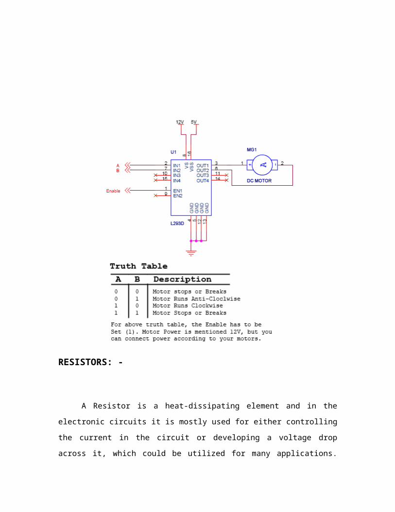
RESISTORS: -
A Resistor is a heat-dissipating element and in the
electronic circuits it is mostly used for either controlling
the current in the circuit or developing a voltage drop
across it, which could be utilized for many applications.

There are various types of resistors, which can be
classified according to a number of factors depending upon:
Material used for fabrication
Wattage and physical size
Intended application
Ambient temperature rating
Cost
Basically the resistor can be split in to the following four
parts from the construction view point.
(1) Base
(2) Resistance element
(3) Terminals
(4) Protective means.
The following characteristics are inherent in all
resistors and may be controlled by design considerations and
choice of material i.e. Temperature co–efficient of
resistance, Voltage co–efficient of resistance, high
frequency characteristics, power rating, tolerance & voltage
rating of resistors. Resistors may be classified as
(1) Fixed
(2) Semi variable
(3) Variable resistor.
CAPACITORS

The fundamental relation for the capacitance between
two flat plates separated by a dielectric material is given
by:-
C=0.08854KA/D
Where: -
C= capacitance in pf.
K= dielectric constant
A=Area per plate in square cm.
D=Distance between two plates in cm
Design of capacitor depends on the proper dielectric
material with particular type of application. The dielectric
material used for capacitors may be grouped in various
classes like Mica, Glass, air, ceramic, paper, Aluminum,
electrolyte etc. The value of capacitance never remains
constant. It changes with temperature, frequency and aging.
The capacitance value marked on the capacitor strictly
applies only at specified temperature and at low
frequencies.
LED (Light Emitting Diodes):
As its name implies it is a diode, which emits light
when forward biased. Charge carrier recombination takes
place when electrons from the N-side cross the junction and
recombine with the holes on the P side. Electrons are in the
higher conduction band on the N side whereas holes are in
the lower valence band on the P side. During recombination,
some of the energy is given up in the form of heat and

light. In the case of semiconductor materials like Gallium
arsenide (GaAs), Gallium phoshide (Gap) and Gallium arsenide
phoshide (GaAsP) a greater percentage of energy is released
during recombination and is given out in the form of light.
LED emits no light when junction is reverse biased.
ULTRASONIC SENSOR
Specifications:
Power Voltage: DC 6-12V
Quiescent Current: less than 2mA
Output Level: high 5V
Output Level: Low 0V
Sensing Angle: no greater than 15°
Sensing Distance: 2mm-3m
Note: The sensing distance varies by smoothness of different
surfaces.

Ultrasonic sensors (also known as tranceivers when they
both send and receive) work on a principle similar to radar
or sonar which evaluate attributes of a target by
interpreting the echoes from radio or sound waves
respectively. Ultrasonic sensors generate high frequency
sound waves and evaluate the echo which is received back by
the sensor. Sensors calculate the time interval between
sending the signal and receiving the echo to determine the
distance to an object.
This technology can be used for measuring: wind speed
and direction (anemometer), fullness of a tank and speed
through air or water. For measuring speed or direction a
device uses multiple detectors and calculates the speed from
the relative distances to particulates in the air or water.
To measure the amount of liquid in a tank, the sensor
measures the distance to the surface of the fluid. Further
applications include: humidifiers, sonar, medical
ultrasonography, burglar alarms and non-destructive testing.
Systems typically use a transducer which generates
sound waves in the ultrasonic range, above 20,000 hertz, by
turning electrical energy into sound, then upon receiving
the echo turn the sound waves into electrical energy which
can be measured and displayed
BATTERY:

An electrical battery is a combination of one or more
electrochemical cells, used to convert stored chemical
energy into electrical energy. Since the invention of the
first Voltaic pile in 1800 by Alessandro Volta, the battery
has become a common power source for many household and
industrial applications. According to a 2005 estimate, the
worldwide battery industry generates US$48 billion in sales
each year, with 6% annual growth.
Batteries may be used once and discarded, or recharged
for years as in standby power applications. Miniature cells
are used to power devices such as hearing aids and
wristwatches; larger batteries provide standby power for
telephone exchanges or computer data centers.
KEILC:
1. Click on the Keil uVision Icon on DeskTop
2. The following fig will appear

3. Click on the Project menu from the title bar
4. Then Click on New Project
5. Save the Project by typing suitable project name
with no extension in u r own folder sited in either
C:\ or D:\

6. Then Click on Save button above.
7. Select the component for u r project. i.e. Atmel……
8. Click on the + Symbol beside of Atmel

9. Select AT89C51 as shown below
10. Then Click on “OK”
11. The Following fig will appear

12. Then Click either YES or NO………mostly “NO”
13. Now your project is ready to USE
14. Now double click on the Target1, you would get
another option “Source group 1” as shown in next
page.
15. Click on the file option from menu bar and select
“new”

16. The next screen will be as shown in next page, and
just maximize it by double clicking on its blue
boarder.
17. Now start writing program in either in “C” or “ASM”

18. For a program written in Assembly, then save it with
extension “. asm” and for “C” based program save
it with extension “ .C”
19. Now right click on Source group 1 and click on “Add
files to Group Source”

20. Now you will get another window, on which by default
“C” files will appear.
21. Now select as per your file extension given while
saving the file
22. Click only one time on option “ADD”
23. Now Press function key F7 to compile. Any error will
appear if so happen.

24. If the file contains no error, then press Control+F5
simultaneously.
25. The new window is as follows
26. Then Click “OK”
27. Now Click on the Peripherals from menu bar, and
check your required port as shown in fig below

28. Drag the port a side and click in the program file.
29. Now keep Pressing function key “F11” slowly and
observe.
30. You are running your program successfully

CONCLUSION
The project “AUTONOMOUS ROBOT” has been
successfully designed and tested. It has been developed by
integrating features of all the hardware components used.
Presence of every module has been reasoned out and placed
carefully thus contributing to the best working of the unit.
Secondly, using highly advanced IC’s and with the help
of growing technology the project has been successfully
implemented.

Finally we conclude that EMBEDDED SYSTEM is an
emerging field and there is a huge scope for research and
development.

BIBLIOGRAPHY
The 8051 Micro controller and Embedded
Systems
-Muhammad Ali Mazidi
Janice
Gillispie Mazidi
The 8051 Micro controller Architecture,
Programming & Applications
-Kenneth J.Ayala
Fundamentals Of Micro processors and
Micro computers
-B.Ram
Micro processor Architecture, Programming
& Applications
-Ramesh S.Gaonkar
Electronic Components

-D.V.Prasad
Wireless Communications
- Theodore S. Rappaport
Mobile Tele Communications
- William C.Y. Lee
References on the Web:
www.national.com
www.atmel.com
www.microsoftsearch.com
www.geocities.com
Ultrasonic Acoustic Sensing Brown University
Laser Ultrasonic Sensor Streamlines Papermaking
Process, Lawrence Berkeley Lab, Dan Krotz
Ultrasonic Flaw Detection for Technicians, Chapter 2,
3rd ed., 2004 by J. C. Drury (~5 pages)
Measure distance using the ultrasonic sensor
Ultra Technology More uniform fibre distribution in
paper with ultrasonics in the paper machine wet end.
Ultrasound transducer entry in the public domain NCI
Dictionary of Cancer Terms


