ASHESI UNIVERSITY AFFORDABLE DIGITAL GUITAR ...
47
ASHESI UNIVERSITY AFFORDABLE DIGITAL GUITAR EFFECTS PEDAL FOR LOCAL GUITARISTS CAPSTONE PROJECT B.Sc. Electrical & Electronic Engineering Victor Hazel 2019 ASHESI UNIVERSITY
-
Upload
khangminh22 -
Category
Documents
-
view
0 -
download
0
Transcript of ASHESI UNIVERSITY AFFORDABLE DIGITAL GUITAR ...

ASHESI UNIVERSITY
AFFORDABLE DIGITAL GUITAR EFFECTS PEDAL FOR LOCAL GUITARISTS
CAPSTONE PROJECT
B.Sc. Electrical & Electronic Engineering
Victor Hazel
2019
ASHESI UNIVERSITY

AFFORDABLE DIGITAL GUITAR EFFECTS PEDAL FOR LOCAL GUITARISTS
CAPSTONE PROJECT
Capstone Project submitted to the Department of Engineering, Ashesi
University in partial fulfillment of the requirements for the award of
Bachelor of Science degree in Electrical & Electronic Engineering.
Victor Hazel
2019

i
DECLARATION
I hereby declare that this capstone is the result of my own original work and that no part of it has been
presented for another degree in this university or elsewhere.
Candidate’s Signature:
……………………………………………………………………………………………
Candidate’s Name:
……………………………………………………………………………………………
Date:
……………………………………………………………………………………………
I hereby declare that preparation and presentation of this capstone were supervised in accordance
with the guidelines on supervision of capstone laid down by Ashesi University
College.
Supervisor’s Signature:
……………………………………………………………………………………………
Supervisor’s Name:
……………………………………………………………………………………………
Date:
……………………………………………………………………………………………

ii
Acknowledgments
I want to express my gratitude to Jehovah for His abundant grace and mercy for a successful project.
I also want to appreciate Dr. Nathan Amanquah for his encouragement even when things were tough.
I want to thank all my colleagues for the help provided in understanding concepts and implementing
them. Special thanks to friends from the DSP class who gave me ideas to overcome challenges faced
during this project.
iii
Abstract
Music has been a mode of communication and a source of identity for many cultures, especially in
Africa. The sound from the guitar is one of the many components that make up music, The electric
guitar is a musical instrument, usually made up of six strings which is connected to amplifiers to
produce sound. Technological advancement has led to the creation of Guitar effects pedals.
However, manufacturers keep making new models of guitar effects pedals with a continuous
increasse in cost. It is therefore difficult for low-income young guitarists to have access to guitar
effects pedals. This project seeks to use a general purpose microcontroller to create a very affordable
guitar effects pedal.

iv
Table of Contents
Acknowledgments ii
Abstract iii
Chapter 1: Introduction 2
Chapter 2: Related Work 6
Chapter 3: Requirements and Design 8
References 33
APPENDIX 37

1
Table of Figures
Figure 1 Functional block diagram of an effects box .......................................................................... 2
Figure 2 A block diagram of N19201 block interfacing with Matlab ................................................. 6
Figure 3 Op-amp based amplifier for input signal ............................................................................. 11
Figure 4 A DC offset circuit .............................................................................................................. 12
Figure 5 A 3-bit flash comparator for ADC ...................................................................................... 13
Figure 6 Binary Weighted DAC ........................................................................................................ 15
Figure 7 8-bits R2R DAC .................................................................................................................. 16
Figure 8 Architecture of Arduino ....................................................................................................... 17
Figure 9 Pin mapping for Arduino Uno ............................................................................................. 18
Figure 10 Pin Mapping for ATMega 2560 ........................................................................................ 19
Figure 11 Full-wave bridge rectifier .................................................................................................. 20
Figure 12 Complete Circuit Schematic .............................................................................................. 23
Figure 13 Implemented Bread Board Circuit ..................................................................................... 24
Figure 14Input Signal: 1Hz, 1V peak-to-peak ................................................................................... 27
Figure 15Amplified Signal vrs Original Signal ................................................................................. 27
Figure 16Amplified Signal, offset at 2.5V vrs Original Signal ........................................................ 28
Figure 17Digital-Analog Converted Signal vrs Original Signal ....................................................... 28
Figure 18 0V offset vrs Original Signal ............................................................................................. 29
Figure 19 Amplified output signal ..................................................................................................... 29
Figure 20 Unprocessed Signal ........................................................................................................... 30
Figure 21 Original Signal(orange) vrs signal with Tremolo effect(blue) .......................................... 30
Figure 22 Impulse response of a reverb system ................................................................................. 31
Figure 23 Original Signal vrs Reverbed Signal ................................................................................. 31
List of Tables Table 1Table of requirement and Specifications ................................................................................. 8 Table 2 Table of inputs and outputs ..................................................................................................... 9

2
Chapter 1: Introduction
There are many stringed instruments used in African music, and the guitar is a classic example. It is
a string instrument which has been used across many different genres of music. As music evolved,
guitarists began using new technology to enhance their play. In 1948, the first commercially
standalone effects unit was made by DeArmond Trem Trol [1]. A guitar effect unit is a device that
modifies the sound of the guitar to produce new tones. Such tones include distortion, chorus, delay,
and flanger. Several other units were produced as the years went by. In the 1980s, the first multi-
effects unit was produced. A guitar multi-effects pedal takes in an analog signal from the guitar,
performs signal processing on the signals and passes the resulting analog signal output through an
amplifier as shown in Error! Reference source not found.as shown in Guitar effect pedals were
made in single units called stomp boxes. Every stomp box was created with a circuit for a one guitar
effect such as distortion stomp boxes. A guitarist will, therefore, have to buy several stomp boxes,
one for each effect tone he desired to have. As such, guitarists had the liberty to mix several tones
(effects) during live play [2]. Guitarists had to arrange many stomp boxes on a pedal board and
interconnect them with a patch cable. Finding the source of feedback when many stomp boxes are
connected then became a problem. The inception of the multi-effects pedal allowed guitarists to carry
all these effects in a single unit. The guitarist will not have to take a long time to connect several
stomp boxes and spend money on buying patch cables. A downside of the multi-effects pedal is that
it is relatively expensive as compared to the stomp boxes. Also, when a part of it gets damaged, the
whole unit has to be replaced, unlike the stomp boxes which a unit can easily be replaced. On the
hand, new multi-effects give guitarists the chance to customize their effects and save it on their pedal.
Figure 1 Functional block diagram of an effects box

3
1.1 Background
The processing of guitar signals with Digital Signal Processes requires a DSP chip. Digital signal
processing involves converting continuous varying quantities such as voltages and temperature into
discrete values for processing. Previously, signal processing was done through the building of
electrical circuits. However, signal processing can now be done digitally, thanks to the invention of
the DSP chip, a high-speed integrated circuit optimized for high-speed huge mathematical
computations [3]. Digital processing involves manipulations of many sampled units of a signal.
Currently, technological advancements have made it possible for the creation of cheap micro-
controllers which can be used to perform digital signal processes. However, the quality of processed
signals by micro-controllers may not be as high as that of a dedicated DSP chip but will be of
acceptable quality. Acceptable quality is the audio quality that has low or little noise compared to the
signal of interest.
Guitar multi-effects are very expensive in Ghana. As a result, most Ghanaian guitarists cannot afford
them. Most guitarists who have an effect pedal find it difficult to buy a newer version due to the cost
involved. Also, the guitar multi-effects are limited to sound from the guitar alone, which has
processed to give a new tone. This project aims at creating an acceptable quality digital effects board
for a guitar which is less than 300.00 GHC. A search on some of Ghana’s retail online shops, OLX
and Tonaton showed that the lowest price of guitar multi-effects is GH¢300.00 and that is for a used
effects pedal. The table below shows the prices of new effects boards.

4
The prices of new effects boards
Brand Cost (GH¢) Site
Roland GR-55s Guitar Effect Pedal 3,000.00 www.ghanabuysell.com
Boss GT 10 Guitar Multi-Effects
Processor
2,000.00 www.tonaton.com
RP90 DigiTech Guitar Effect 1,900.00 www.ghanabuysell.com
Boss GT 10 Guitar Multi-Effects
Processor
2,000.00 www.tonaton.com
This project will employ the use of a general-purpose microchip for the processing of signals:
ATmega2560. The price of an ATmega2560 chip on an Arduino costs not more than GH¢60.00. The
other components required for building the circuits and developing the whole product will not cost
more than a GH¢100.00. It is, therefore, possible to produce on a large scale at a price less than
GH¢300.00. A digital effect pedal that costs GH¢300 will be the same price of an average used effects
board 50% less than the price of some second-hand effects pedals. This price will be competitive on
the market and will be preferred for the large middle-income guitarists in Ghana.
1.2 Scope of Work/Research
1) Building Circuits
2) Signal processing of analog signals to produce different tones
3) Testing the entire project
The final product will be a standalone guitar multi-effects board. A standalone guitar multi-guitar
effects pedal is a separate unit. It will take an input signal from the guitar and perform some
algorithms on the signal to produce a new effect.

5
1.3 Significance And Contribution/ Outcome
As a guitarist myself, I understand the influence of having an effects pedal and how it changes the
way I play. It revolutionizes my playing. I do not want other guitarists to be unable to experience this
revolution, just because it is too expensive. My project will make this experience more affordable for
guitarists, and in doing so, tap into deeper potentials previously unknown.

6
Chapter 2: Related Work
Digital signal processing has been done in several ways over the years. Options include software
digital signal processing and hardware signal processing. Software has made it possible to process
digital systems with mathematical filters to perform signal processes. MATLAB and Simulink
provide a platform for analysis and processing of signals. The Data Acquisition toolbox in Matlab
helps to make this real time. The hardware necessary for this is the NI 9201 board, NI 9263 board
and an audio amplifier. MATLAB also provides a complete workflow for fixed-point design and C
and HDL code generation. The benefit of using MATLAB is that it requires very little hardware and
that Simulink provides a graphical interface for processes [4]. Error! Reference source not found.
illustrates how the filter, DSP card, and Matlab are used for signal processing.
A project by Czubak et al. in making a real-time digital effects system used MATLAB Simulink to
design the filters [5]. According to them, MATLAB Simulink allows for fast calculation and
representation of filter designs. MATLAB Simulink provides building blocks which contains the
necessary mathematical calculations for creating filters. A DSP board together with Code Composer
3.1 made it possible for real-time demonstration.
Figure 2 A block diagram of N19201 block interfacing with Matlab

7
Another project carried out by Kevin Salvador employed a TI/Spectrum digital DSK6713 for digital
signal processing on guitar signals [5]. Again, MATLAB was used to perform signal processing on
the signals.

8
Chapter 3: Requirements and Design
This project focused on enhancing customer usage in the local industry and the ability of customers
to purchase guitar effects pedals. As a result, an analysis of customer needs for the product. The
requirements of this project consist of the customer requirements and design requirements. The
requirements will be updated as the project progresses.
3.1 Design requirements and specifications with justification
Table 1Table of requirement and Specifications
Requirement Specification Justification
Light in weight Less than 4.5Kg The product must be light
enough to be carried around
Audio output must be clear The output must be of high
quality.
This is to prevent distorted
audio signals from the
amplifier
Portable Product size must be no more
than (20 x 20 x 5) cm3
It should be small enough to
be carried in a guitar bag
Cost The product must not be
more than 300.00 cedis
Most guitarists wish to spend
less than 400 cedis on an
effects board of this caliber

9
User friendliness Controls should be simple
and should be easy to
connect and play
Guitarists like to connect and
play on the spot.
Power Supply 5V and -5V output The different blocks require
5V or -5V for operation
Inputs and outputs
Table 2 Table of inputs and outputs
Inputs Outputs
Guitar Analog signal Analog signal with effects
Power supply Different power levels for various components
Volume control /Gain Amplification Varying volume levels from no volume to
highest volume
Function Switches Cause the microcontroller to switch between
different effects
Equalizer Controls the bass, mids, and highs of the tone.
10
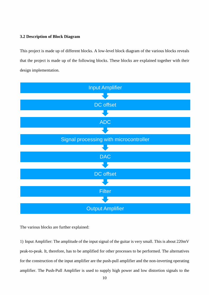
3.2 Description of Block Diagram
This project is made up of different blocks. A low-level block diagram of the various blocks reveals
that the project is made up of the following blocks. These blocks are explained together with their
design implementation.
The various blocks are further explained:
1) Input Amplifier: The amplitude of the input signal of the guitar is very small. This is about 220mV
peak-to-peak. It, therefore, has to be amplified for other processes to be performed. The alternatives
for the construction of the input amplifier are the push-pull amplifier and the non-inverting operating
amplifier. The Push-Pull Amplifier is used to supply high power and low distortion signals to the
Output Amplifier
Filter
DC offset
DAC
Signal processing with microcontroller
ADC
DC offset
Input Amplifier

11
load. It consists of two transistors which push and pull the signal on the output signal on the positive
and the negative half cycle respectively [6]. The advantages of this amplifier are low distortion,
absence of magnetic saturation and cancellation of power supply ripples [7]. The push-pull amplifier
needs to have identical transistors and requirement coupling transformers. The output of a non-
inverting amplifier is in phase with the input signal.
The alternative is the non-inverting amplifier using an operational amplifier. The non-inverting
amplifier has a high input impedance and low output impedance. This makes it a good circuit buffer
to protect the source of the audio signal from overloading by the rest of the circuit.
The non-inverting Operational Amplifier was selected. This is due to its ability to protect the
incoming signal source from the rest of the circuit. The operational amplifier is an all one built device
with transistors which is performs can be used as an amplifier or a switch. It is light in weight, small
in size and more cost-effective as compared to the push-pull amplifier. The non-inverting operational
amplifier circuit is shown in Figure 3 below.
Figure 3 Op-amp based amplifier for input signal

12
The circuit in Figure 3 shows the implementation of the non-inverting amplifier. The potentiometer
(RV2) which is connected to the ground input from the guitar gives the user the flexibility to adjust
the gain of the signal.
2) DC-OFFSET: This block sets the offset voltage for oscillation of incoming signals. By
default, audio signals from guitars oscillate about 0V. If this wishes to be changed, a DC offset is
built. The incoming signal is capacitor coupled to a potential divider whose voltage is at the desired
offset voltage. The addition of the two signals enables an oscillated at the DC voltage. From Error!
Reference source not found., the capacitor receives the input signal, and the output is signal goes
through the intersection of the capacitors and resistors. The circuit of a DC offset is shown in Figure
4 below.
Figure 4 A DC offset circuit
3) ADC – The Analog to digital converters transforms continuous varying signals to discrete signals
to enable the microcontroller to process it. The design options considered for this block are the flash
ADC

13
Figure 5 A 3-bit flash comparator for ADC
Flash ADC is the fastest type available. It is made up of comparators and a string of resistors. A flash
analog to digital converter uses 2n-1 comparators where n is the number of bits of the ADC. This
means, for an 8 bit ADC which this project seeks to employ will require 255 comparators. This circuit
compares the input signal to a unique reference voltage at each point. The output from each
comparator is an input to a priority encoder circuit. The encoder then outputs the binary equivalent.
[8]. An example of a 3-bits flash comparator is shown in Figure 5 as an illustration.
Regardless of the speed of flash ADC’s, they tend to draw significant current due to the number of
comparators required. The Flash ADC is not economically suitable for this project due to the high
cost in component required [9].

14
Another design alternative is to use the in-built Arduino commands for DSP. The Arduino Mega has
pins that can read analog signals. The command used is ‘AnalogRead().’ This command accepts
analog signals and assigns them a value between 0 and 1023. This suggests that it is a 10 bit ADC. It
does so at a frequency of 8000Hz. The frequency required for this project is 40,000Hz. The Arduino
This means that the sampling frequency of the ADC is not high enough to reproduce the signal to the
quality expected.
The final design option is the to use of bitwise operations to directly program the registers of the
ATMEGA chip. This procedure bypasses the ‘AnalogRead’ command and gives the user the
flexibility to change the sampling frequency by programming the ADC registers and other registers.
It, however, requires more programming skill due to the complex code writing involved.
The latter design option (Bitwise operation) was implemented. This is due to the low cost, and no
extra components required. This project prioritizes low cost. Therefore, a faster process was traded
for a cheaper process.
4) DAC – The DAC block is responsible for converting the processed digital signal to analog
signals. In other words, it converts binary data to voltage or current. In this project, the Digital audio
data would have to be converted to voltage to be heard by the ear. The design options being considered
are the binary-weighted-input DAC and the R-2R binary ladder.
The binary-weighted-input DAC works on the principle of the inverting summing opamp. For three
different voltage input with voltages V1, V2 and V3 into the opamp with resistors R1, R2 and R3
respectively and feedback resistor Rf, the output voltage can be calculated using the equation of the
inverting amplifier. Equation of the inverting amplifier is
−𝑉𝑜𝑢𝑡 = (𝑅𝑓
𝑅𝑖𝑛) ∗ 𝑉𝑖𝑛
Therefore, the output voltage of the summing amplifier is

15
−𝑉𝑜𝑢𝑡 = (𝑅𝑓
𝑅𝑖𝑛𝑉1 +
𝑅𝑓
𝑅𝑖𝑛𝑉2 +
𝑅𝑓
𝑅𝑖𝑛𝑉3)
The binary weighted ADC uses a doubled value of each input resistor Rin as shown in Figure 6. That
is, R1= 1KΩ, R2= 2KΩ, and R3=4KΩ. This suggests that, for an 8bit, resistors will be required in ½
ratio of each pair up to the resistor value 2(n-1) which is 27=128KΩ. This can be limiting if all the
values of resistors are not available [10].
Figure 6 Binary Weighted DAC
The second design alternative for the DAC block is the R-2R ladder. It uses only two values of
resistors with values R and 2R no matter the number of bits of DAC being constructed. It is fairly
simple to use since the output impedance of the ladder is equal to R. The R-2R loader circuit is
analyzed by Thevenin's theory. D0 is voltage-divided. The voltage is simply D0/2. The Thevenin
equivalent resistance (when the source is removed) at that point is two Rs in series 2R. It is realized
that there is another voltage divider circuit showing up. There is a repetitive occurrence of this shape.
Continuing the calculation reveals that the Thevenin equivalent resistance is always R. To know the
weight of voltage each input voltage we use Thevenin's open voltage. In the first stage, D0 (LSB)
was reduced by half; It keeps reducing by a ratio of ½ throughout the circuit. Hence for a 4 bit DAC,
the LSB will contribute D0/16.
The total output voltage is the weighted average of all the input voltages:
𝐴𝑜𝑢𝑡 =𝐷0
16+𝐷1
8+𝐷2
4+𝐷3
2

16
Figure 7 8-bits R2R DAC
Figure 7 is an LTSpice simulation of an 8bit R-2R DAC. The digital value written to it is 00010011.
The output voltage was passed through a non- inverting amplifier which serves as a buffer to the
circuit as well as amplifying the output.
Micro-controller –The microcontroller is responsible for the processing of digital signals to produce
the desired output signals. The microcontroller has General Input/Output pins (GPIO) which are
necessary to interact with signals in the real world. This project will consider two microcontrollers
from the same family: The Arduino Uno and the Arduino Mega. Figure 8 shows the general
architecture of the Arduino.

17
Figure 8 Architecture of Arduino
[11]
Arduino is an open-source easy-to-use platform for building electronic projects. It has a
programmable controller and an Integrated Development Environment which is used to write and
upload instructions unto the controller [12]. The Arduino Uno controller has two memories: program
memory which stores code and data memory which stores data. The main IC is ATmega328(. The
Atmega328 has 32KB of flash memory for storing code, 2KB of SRAM and 1KB of EEPROM and
operates with a clock speed of 16MHz [13]. Arduino Uno has 14 GPIOs (general input-output pins)
which allow the connection of sensors, actuators, and other electrical components.

18
Figure 9 Pin mapping for Arduino Uno
[14]
The Arduino Mega is an advanced model of the Arduino Uno microcontroller. The microchip of the
Arduino Mega is ATmega2560 ( Pin mapping shown in Figure 10). The Arduino Mega has 54
input/output pins and has 256 kB of flash memory. It also has 16 analog pins and 14 pulse width
modulation (PWM) pins [15].
The Arduino Mega was selected for this project due to its large flash memory as compared to the
Uno. This decision was taken because some signal processing requires the use of buffers which may
take up quite a large amount of memory.
Both the Arduino Uno and Mega have the ability to sample analog signals with the command
'AnalogRead,’ which samples analog signals. It, however, does so at a rate of 8kHz. The goal of the
project is to sample at about 40kHz. For this reason, bitwise operations had to be made to registers
directly and interrupts used to run commands.

19
Figure 10 Pin Mapping for ATMega 2560
[16]

20
a. Power supply: The power supply will provide the right power to the various components of
the product. This includes the micro-controller and the amplifier and the DC buffer. This project seeks
to reduce the cost guitarists spend on their effects pedals. Hence, a power supply is designed which
takes 230V AC and outputs a DC voltage for the operation of the device as opposed to the buying of
batteries. This project needs a +5V and -5V supply. A full-wave bridge rectifier allows for DC
generation on both the positive and negative half cycles. The average voltage output is, therefore,
higher than the half wave rectifier’s output. This circuit as shown in Figure 11, makes use of a center
tapped transformer, and four power diodes arranged such a way that, for every half cycle, a pair of
diodes allow current to be rectified to produce a positive voltage on the positive cycle and a negative
voltage on the negative cycle. A smoothing capacitor is connected across the load to smoothen ripples
in the rectified current.
Figure 11 Full-wave bridge rectifier
For this project, the full wave bridge rectifier was chosen because it provides both positive and
negative voltages which are required for the functioning of some blocks.

21
Chapter 4: Implementation, Tests, and Results
Implementation
This project consists of two main parts: the hardware component and the software component
(firmware). The hardware component consists of the physical and tangible parts of the project. This
is mainly composed of the electrical circuit component. The main electrical components used are
resistors, capacitors, and op-amps. This project avoided the use of pre-made modules to allow for
more flexibility and to keep the cost as low as possible. The software consists of computer programs
and the firmware of the micro-controller. Software used include LTSpice, MATLAB, Arduino IDE.
Proteus was used to design the schematic for this project. In this section, the circuitry and software
are explained.
4.1 Hardware
There are four main circuits in this project: The input circuit, the Digital-to-Analog converter, the
output circuit and the power supply circuit.
4.1.1 Input Circuit
This circuit is responsible for receiving the guitar signal and get it ready for the micro-controller to
sample and perform signal processes. This circuit consists of a ¼ guitar input jack which receives the
cable from the guitar. Since the guitar produces a low voltage signal, about 1VRMS max, it needs to
be amplified. The amplifier built is a non-inverting amplifier. The potentiometer is connected to the
ground of the input jack which is connected to the feedback resistor. The purpose of the potentiometer
is to get to be able to control the gain of the signal such that no signals are cut off. The inability to
get a fixed resistor of the exact value required to keep the signal at an amplitude of 2.5V also
influenced the use of the potentiometer. The signal is then passed through a non-inverting operational
amplifier. The amplifier used is the UA741CP general purpose operational amplifier. The amplified
signal is then passed through the DC offset which holds the signal oscillating about 2.5V. This is

22
important because the micro-controller reads a maximum voltage of 5V. If the signal oscillates about
0V, the lowest amplitude will be 0V - 2.5V = -2.5V and which will not be read by the controller,
thereby leading to aliasing. However, when the DC offset is set to 2.5V, the lowest amplitude will be
2.5V - 2.5V = 0V and the highest amplitude will be 2.5V + 2.5V = 5V. The micro-controller will be
now be able to read all values of the incoming signal. From the DC offset, the signal goes to pin A0
of the Arduino Mega.
4.1.2 Output Circuit
After the processing has been done on the Arduino, the output is passed to the R-2R ladder DAC.
The R-2R method was chosen because of the readily availability of the components required. This is
an arrangement of resistors which takes digital bits, weights them and sums them to produce a voltage
between 0 and 5V (We are using 5V because the Vmax for Arduino is 5V). The DAC built is an 8-bit
meaning it has 28 =256 levels between 0V and 5V. This means the digital signal coming is between
0 and 256 and will be converted into a voltage between 0 and 5V.
All the digital pins were connected to each section of the resistor ladder. Since this is a DAC, the
digital signal was manually supplied (ie. between 0 and 225); Where 0 = 0V and 255 = 5V. Every
pin on PORT D (Digital Input and Output Port) contributes to the digital value. The weighted binary
sum of the pins on the port make up the digital value being supplied to the DAC.
The voltage output is given by 𝑑𝑖𝑔𝑖𝑡𝑎𝑙𝑣𝑎𝑙𝑢𝑒
255∗ 5𝑉. The period of a signal is the duration of each step *
the number of steps. For example, if I sample and hold a signal for 5us, (still using an 8-bit DAC),
then the total number of steps is 256. Then the period is
(50*10-6)s*256 steps = 0.0128s. Frequency is the inverse = 78Hz.
The value of R=10KΩ 2R=20KΩ. The DAC is connected to the Arduino Mega by connecting the
DAC inputs to Port C. The

23
Figure 12 Complete Circuit Schematic

24
Figure 13 Implemented Bread Board Circuit
4.2 FIRMWARE
The code was written in C/C++ using the Arduino IDE. It is code modified from a project by Amanda
Ghassaei in 2012. Bitwise operations were performed on the ADC registers to configure them for
operation. The code has an integer variable; ‘effects’ which determines the effects that will be
operating. Delay, Tremolo, Reverb. Clean Boost.
1) Delay: A delay buffer was created to store 7,200 samples. These samples are stored into three
different buffers named buffer_write_index1, buffer_write_index2, buffer_write_index3.
Each buffer stores 1/3 of the 7,200 samples. At any time t, the new sample is added to the
value at buffer_write_index1, buffer_write_index2, buffer_write_index3. The samples in

25
each buffer are played differently with different magnitude scales to determine the amplitude
of the delay.
Pseudo-code for delay:
• The processor reads the next sample, Sn, from the ADC
• It reads the value, Br, at the current read index in the buffer.
• It adds the Sn to Br and writes the output to the DAC
• It writes the value Sn to the buffer at indices, Bw1, Bw2 and Bw3, where:
• Bw1 = Br + (7200/3)
• Bw2 = Br +2*(7200/3)
• Bw3 = Br + 3*(7200/3)
• It then increases Br by one
• Definitions:
- Sn: Current sample value from ADC
- Br: Current read index of delay buffer
- Bw1: Current write index for first delay in buffer
- Bw2: current write index for second delay in buffer
- Bw2: current write index for third delay in buffer
2) Clean boost: This effect type boosts the sound of the clean guitar. Only the amplitude of the
signal is affected. It is achieved by the circuit amplification of the signal. No manipulation
was made in the software to increase the amplitude because the circuit amplification gets the
signal close enough to the clipping amplitude.

26
3) Tremolo: This is a modulation effect that rhythmically changes the amplitude of the signal. A
low-frequency oscillator is convolved with signal which results in the signal oscillating. [17]
Pseudo code for tremolo
• The user inputs the tremolo depth and time, which will be used to determine the parameters,
f and C in the equation: V(t) = Asin(2*pi*f*t) + C.
• The processor reads the next sample, Sn, from the ADC
• The volume coefficient, Vc, is determined from the equation for V(t)
• The output, Vc * Sn, is written to the DAC
4) Reverberation:
Pseudo code:
• The impulse response for a reverb room was recorded and saved in an array on the
processor.
• The processor then reads values from the ADC into a buffer and convolves impulse
response of the reverb, with the values stored in the buffer. It then writes this output to the
DAC
27
Tests and Results
To test the circuit, A sinusoidal signal of 1Hz was passed into the input of the circuit by the wave
generator of analog discovery 2. The output was recorded when the signal passed through each block.
All graphs are plotted together with the original input signal (yellow graph).
Input signal:
Figure 14Input Signal: 1Hz, 1V peak-to-peak
The input signal has an amplitude of 1V and a frequency of 1Hz. The scope of the signal is taken at
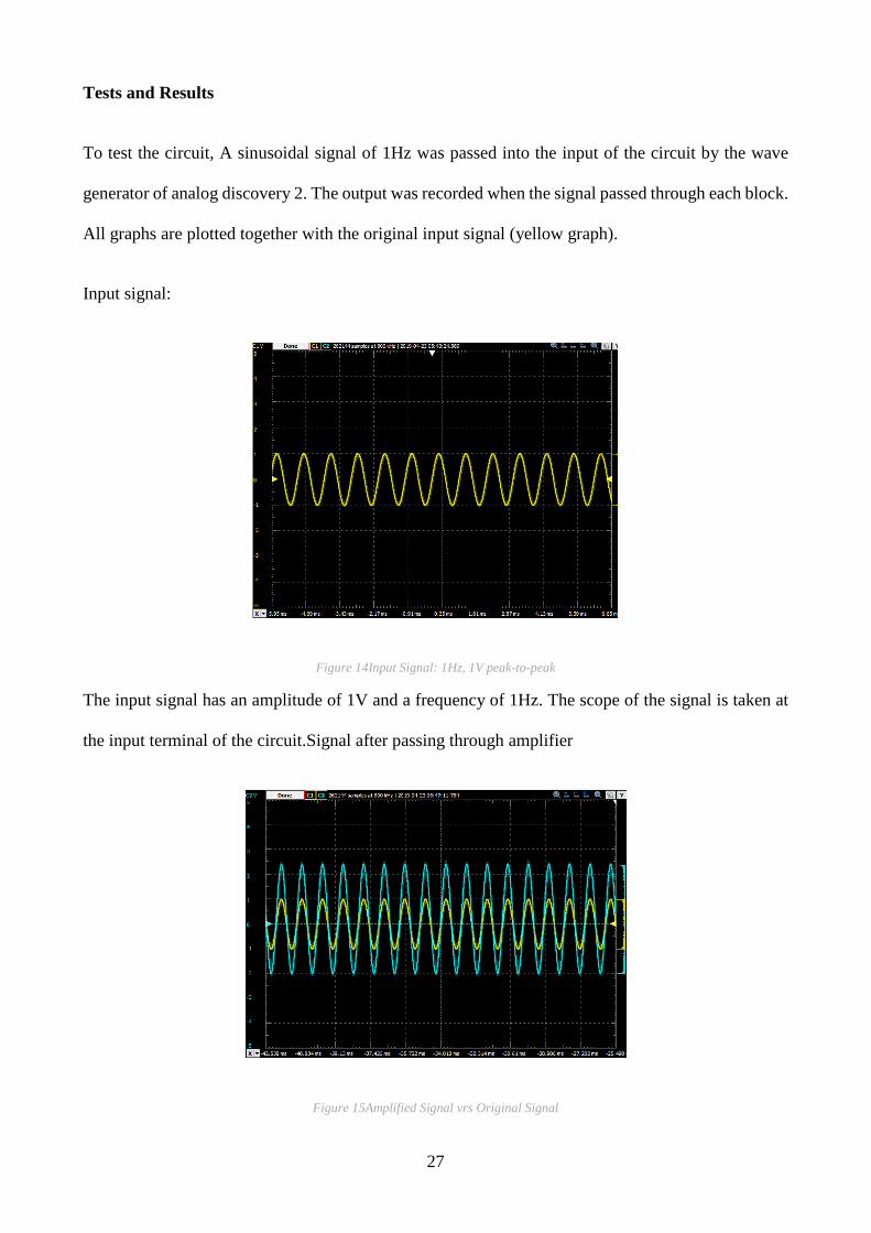
the input terminal of the circuit.Signal after passing through amplifier
Figure 15Amplified Signal vrs Original Signal

28
The signal passes through the amplifier. The amplified signal (blue) still oscillates about 0V and is in
phase with the input signal.
After 2.5V DC offset
Figure 16Amplified Signal, offset at 2.5V vrs Original Signal
The signal then passes through a 2.5 DC offset. This causes the signal to oscillate about 2.5V. This is
necessary for the Arduino Mega to be able to sample the signal since the signals above 5V and below
0V cannot be read.
After DAC (Notice vivid steps in signal)
Figure 17Digital-Analog Converted Signal vrs Original Signal

29
After the signal is processed by the microcontroller, it passes through a DAC to convert the signal
back to an analog signal. This is evident in the visible ripples in the signal (amplified signal oscillating
about 2.5V). The ripples are as a result of sampling of the input signal phase.
Figure 18 0V offset vrs Original Signal
The analog signal passes through a 0V DC buffer. This causes the signal to oscillate about 0V. This
is necessary to reduce the noise in the output. The signal is still in phase with the original input signal.
Figure 19 Amplified output signal

30
The signal is finally amplified through an output amplifier. The signal final signal is an amplified
version of the input signal and is still
in phase.
The effects were tested in MATLAB before their implementation in the arduino environment. Due to
memory issues, some could not be implemented. This signal was used for the testing of the effects
that were generated.
Figure 20 Unprocessed Signal
Figure 21 Original Signal(orange) vrs signal with Tremolo effect(blue)
For the implementation and testing of the reverberation effect, an impulse response was generated
for an impulse input in a room with reverb. The impulse input used was a snare drum.

31
Figure 22 Impulse response of a reverb system
Figure 23 Original Signal vrs Reverbed Signal

32
Chapter 4: Future improvement, limitations, conclusion
This project can be extended to have more effects like distortion, flanger, fuzz, etc. A voice box effect
can be incorporated to create a new sound effect. For this to be achieved, there is a need for a second
analog to digital converter for the microphone. There are two separate ADCs for the microphone and
guitar signal because they will have to be working simultaneously. After these signals are processed,
they will be an input into the micro-controller where processing will on the digital signals. At this
block, the equalizer, volume and function switches can be used as to affect the output sound. System
memory stores the functions and commands for operation by the microprocessor. The final digital
signal produced by the microcontroller is converted to an analog signal and sent to an amplifier.
Wireless transfer of signals is also a feature that can be explored. Bluetooth communication might be
an option to achieve.
Some limitations faced in this project was lack of sufficient memory for the Arduino. Again, noise in
the output signal was expected to be generated from loose breadboard connections.
This project has been a learning experience and has been a successful proof of concept. This project
can be pursued to create a marketable product.

33
References
[1] Sun Power UK, "A Brief History of Guitar Effects Pedals [Infographic]," 2018. [Online].
Available: https://www.sunpower-uk.com/a-brief-history-of-guitar-effects-pedals-
infographic/. [Accessed 18 January 2019].
[2] Guitar Fella, "Multi-Effects Devices vs. Guitar Pedals," 2018. [Online]. Available:
https://www.guitarfella.com/multieffects-versus-pedals/. [Accessed 18 January 2019].
[3] Small Business, "The Basics of a DSP Processor," Smallbusiness.chron.com, 2019.
[Online]. Available: https://smallbusiness.chron.com/basics-dsp-processor-28218.html.
[Accessed: 18 January 2019].
[4] MathWorks, "System Objects to Stream Live Data to and from Data Acquisition
Interfaces", mathworks.com, 2019. [Online]. Available:
https://www.mathworks.com/examples/matlab/community/35752-system-objects-to-
stream-live-data-to-and-from-data-acquisition-interfaces. [Accessed: 18 January 2019].
[5] ResearchGate, "Guitar Effects Processor Using DSP," 2019. [Online]. Available:
https://www.researchgate.net/publication/241869333_Guitar_Effects_Processor_Using_
DSP. [Accessed: 18 January 2019].
[6] "Push Pull Amplifier Circuit Diagram - Class A, Class B and Class AB Amplifiers",
circuitdigest.com, 2019. [Online]. Available: https://circuitdigest.com/electronic-
circuits/push-pull-amplifier-circuit-diagram. [Accessed: 23- Apr- 2019].

34
[7] "Push pull amplifier, working and theory. Class A , Class B , Class AB circuit diagram",
Electronic Circuits and Diagrams-Electronic Projects and Design, 2019. [Online].
Available: http://www.circuitstoday.com/push-pull-amplifier. [Accessed: 23- Apr- 2019].
[8] T. ARTICLES et al., "Flash ADC | Digital-Analog Conversion | Electronics Textbook",
Allaboutcircuits.com, 2019. [Online]. Available:
https://www.allaboutcircuits.com/textbook/digital/chpt-13/flash-adc/. [Accessed: 23-
Apr- 2019].
[9] S. Ball, "Analog-to-Digital Converters", EE Times, 2019. [Online]. Available:
https://www.eetimes.com/document.asp?doc_id=1276974. [Accessed: 23- Apr- 2019].
[10] "The Summing Amplifier", Electronics Tutorials, 2019. [Online]. Available:
https://www.electronics-tutorials.ws/opamp/opamp_4.html. [Accessed: 23- Apr- 2019].
[11] S. Basu, "What is Arduino? Arduino vs. Raspberry Pi. All you need to know |H2S Media",
H2S Media, 2019. [Online]. Available: https://www.how2shout.com/what-is/what-is-
arduino-arduino-vs-raspberry-pi-all-you-need-to-know.html. [Accessed: 23- Apr- 2019].
[12] Spark Fun, "What is an Arduino? - learn.sparkfun.com", learn.sparkfun.com, 2019.
[Online]. Available: https://learn.sparkfun.com/tutorials/what-is-an-arduino. [Accessed:
18- Jan- 2019].
[13] Electronic Projects for Engineering Students, "Overview of Ardunio Microcontroller with
Working Principle and Design", ElProCus - Electronic Projects for Engineering Students,
2019. [Online]. Available: https://www.elprocus.com/arduino-basics-and-design/.
[Accessed: 18 January 2019].
[14] "Arduino - PinMapping168", arduino.cc, 2019. [Online]. Available:
https://www.arduino.cc/en/Hacking/PinMapping168. [Accessed: 23- Apr- 2019].

35
[15] "Arduino Comparison Guide - learn.sparkfun.com", learn.sparkfun.com, 2019. [Online].
Available: https://learn.sparkfun.com/tutorials/arduino-comparison-guide/megas-arms-
ynsoh-my. [Accessed: 23- Apr- 2019].
[16] "Arduino - PinMapping2560", Arduino.cc, 2019. [Online]. Available:
https://www.arduino.cc/en/Hacking/PinMapping2560. [Accessed: 23- Apr- 2019].
[17] K. Pearsall, "What is Tremolo?", Fender.com. [Online]. Available:
https://www.fender.com/articles/tech-talk/pedal-board-primer-get-to-know-tremolo. [Accessed: 23-
Apr- 2019]

36

37
APPENDIX
Code
//Half Frequency Playback
//by Amanda Ghassaei
//https://www.instructables.com/id/Arduino-Vocal-Effects-Box/
//July 2012
/*
* This program is free software; you can redistribute it and/or modify
* it under the terms of the GNU General Public License as published by
* the Free Software Foundation; either version 3 of the License, or
* (at your option) any later version.
*
*/
int effect = 2;
// Parameters for delay
// Parameters for tremolo effects
// User-defined parameters
float tremolo_time = 0.1; // s
float tremolo_depth = 0.8;
// Calculated parameters
float tremolo_frequency = 1 / tremolo_time;
float tremolo_peak = 3;
float tremolo_amplitude = tremolo_peak / 2;

38
float tremolo_offset = 2*tremolo_amplitude - tremolo_amplitude*tremolo_depth;
float tremolo_multiplier = 1;
float pi = 3.14159265358979323846;
//audio storage
const unsigned long sample_rate = 9000; // Hz
const unsigned long buffer_size = 0.8 * sample_rate;
byte delay_buffer[buffer_size];
byte incomingAudio;//storage variable
unsigned long buffer_read_index = 0;
unsigned long buffer_write_index1 = buffer_read_index + buffer_size / 3 - 1;
unsigned long buffer_write_index2 = buffer_read_index + (buffer_size / 3) * 2 - 1;
unsigned long buffer_write_index3 = buffer_read_index + (buffer_size / 3) * 3 - 1;
float magScale1 = 0.8;
float magScale2 = 0.8;
float magScale3 = 0.8;
byte get_from_buffer(unsigned long index)
return delay_buffer[index];
void append_to_buffer(unsigned long index, byte new_value)
delay_buffer[index] = delay_buffer[index] + new_value;

39
void remove_from_buffer(unsigned long index)
delay_buffer[index] = 0;
void setup()
DDRC = B11111111;
DDRF = B00000000;
cli();//diable interrupts
//set up continuous sampling of analog pin 0
//clear ADCSRA and ADCSRB registers
ADCSRA=0;
ADCSRB = 0;
ADMUX |= (1 << REFS0); //set reference voltage
ADMUX |= (1 << ADLAR); //left align the ADC value- so we can read highest 8 bits from ADCH
register only
ADCSRA |= (1 << ADPS2) | (1 << ADPS0); //set ADC clock with 32 prescaler- 16mHz/32=500kHz
ADCSRA |= (1 << ADATE); //enabble auto trigger
ADCSRA |= (1 << ADIE); //enable interrupts when measurement complete
ADCSRA |= (1 << ADEN); //enable ADC

40
ADCSRA |= (1 << ADSC); //start ADC measurements
sei();//enable interrupts
Serial.begin(9600);
ISR(ADC_vect) //when new ADC value ready
incomingAudio = ADCH;//
// This is the delay effect
if (effect == 0)
// Play incoming signal plus delay at that point
PORTC = get_from_buffer(buffer_read_index) + incomingAudio;
remove_from_buffer(buffer_read_index);
// Store delayed signals
append_to_buffer(buffer_write_index2, incomingAudio * magScale2);
append_to_buffer(buffer_write_index3, incomingAudio * magScale3);
// Increment buffer indexes
buffer_read_index = (buffer_read_index + 1) % buffer_size;
buffer_write_index1 = (buffer_write_index1 + 1) % buffer_size;
buffer_write_index2 = (buffer_write_index2 + 1) % buffer_size;
buffer_write_index3 = (buffer_write_index3 + 1) % buffer_size;

41
// This is the tremolo effect
if (effect == 1)
tremolo_multiplier = tremolo_amplitude * sin(2*pi*tremolo_frequency*micros()*pow(10,-6)) +
tremolo_offset;
PORTC = tremolo_multiplier * incomingAudio;
Serial.println(tremolo_multiplier);
// This is the clean guitar(no effect)
if (effect == 2)
PORTC =incomingAudio;
void loop()