
(Advances in Solid State Physics 24) T. Patrick Martin (auth ...
355
FESTKORPERPROBLEME XXIV ADVANCES IN SOLID STATE PHYSICS
-
Upload
khangminh22 -
Category
Documents
-
view
4 -
download
0
Transcript of (Advances in Solid State Physics 24) T. Patrick Martin (auth ...

FESTKORPERPROBLEME XXIV
ADVANCES IN SOLID STATE PHYSICS
FESTKORPER PROBLEME XXlV ADVANCES IN SOLID STATE PHYSICS
Plenary Lectures of the 48th Annual Meeting of the German Physical Society (DPG) and of the Divisions "Semiconductor Physics" "Metal Physics" " ' Low Temperature Physics" "Thermodynamics and Statistical Physics" "Thin Films" "Surface Physics" "Magnetism" "Physics of Polymers" "Molecular Physics"
MiJnster, March 12 ... 17, 1984
Edited by P. Grosse, Aachen
With 233 figures
Vieweg
ISSN 0430-3393
All rights reserved �9 Friedr. Vieweg & Sohn Verlagsgesellschaft mbH, Braunschweig 1984
No part of this publication may be reproduced, stored in a retrieval system or transmitted, mechanical, photocopying or otherwise, without prior permission of the copyright holder.
Set by Vieweg, Braunschweig Printed and bound by W. Langeliiddecke, Braunschweig Cover design: Barbara Seebohm, Braunschweig
ISBN 3-528-08030-2
Foreword
In 1984 the Solid State Physics Division of the German Physical Society again has organized its spring meeting together with the 48th Annual Plenary Conference of the society. The conference was really a great success; .about 2500 physicists came to MOnster. In spite of the large number of participants it was possible to find many changes to communicate with colleagues.
Volume XXIV of the "Festk6rper-Probleme" contains a selection of the plenary talks and invited talks of the conference.
This year the talk of the winner of the Walter-Schottky-prize 1984 is not included in the volume, since the prize was awarded to G. H. D6hler, who had contributed the paper "n-i-p-i doping superlattices" to volume XXIII last year.
The first two papers are dedicated to one of the most fascinating fields in modem solid state physics: Physics of microclusters (Martin), experiments and theoretical models to study the properties of crystals "ab initio" when they are growing from atoms or molecules to a large crystal. The second topic is the quantum Hall-effect (St6rmer), which was previously discussed by the Walter-Schottky-prize winner K. v. Klitzing in Vol. XXI of this series. Lower temperatures and samples of higher quality now allow experiments which show surprising effects related to fractional quantum numbers. Those effects may be explained by a collective behavior of the electron gas. The next three papers report on unconventional systems: Hydrogen in metals (Peisl), i.e. crystals in which the protons and not only the electrons play an important role, and further conducting polymers (Roth) and amorphous silicon (Fuhs). In two contributions the physics of defects in silicon is discussed (Watkins, Wagner). This complicated subject is today of large interest because of the importance of defects in silicon applied in microelectronics.
Most of the articles concern physics of interfaces and surfaces. Progress in experi- mental technique of surface analysis and of preparation methods, as well as the activities in thin layer- and microstructure technology have increased the interest in this field: optical and tunneling spectroscopy (Abel6s, Ewert), sputter-depth- proffiing (Oechsner), and light scattering (Abstreiter) to analyze surfaces and inter- faces, and one paper about the surfaces of the III-V-compounds (Mtinch).
The last two papers report on applied problems: one concerns high speed field effect transistors (Heime), an excellent example for the success of tailor-made
V
semiconductor materials by means of the application of the molecular beam epitaxy technique. The other article concerns miniature refrigerators (Heiden), very often the bottle neck for technical applications of modem solid state devices, working at low temperatures.
Following the suggestions of the readers of the Festk6rperprobleme-series we include an author-index of "Festk6rperprobleme", volumes I...XXIV into volume XXIV. This may help the reader to find references in a list of more than 300 authors!
The editor again thanks the authors and the publisher for their collaboration. In particular I acknowledge the cooperation of Mr. A. Schubert from Vieweg-Verlag and the assistance of my coworker Mr. J. Brunn in the course of reading and revising the manuscripts.
Finally I thank my colleagues in Aachen and in other places for their support in preparing the program and for their collaboration at the conference.
Aachen, May 1984
Peter Grosse
VI
Contents
T. Patrick Martin The Structure of Elemental and Molecular Clusters . . . . . . . . . . . . . . . . . . 1
Horst L. St6rmer The Fractional Quantum Hall Effect . . . . . . . . . . . . . . . . . . . . . . . . . . . 25
Johann Peisl Lattice Distortion, Elastic Interaction, and Phase Transitions of Hydrogen in Metals . . . . . . . . . . . . . . . . . . . . . . . . . . . . . . . . . . . . . 45
Siegfried Ewert
Inelastic Electron Tunneling Spectroscopy . . . . . . . . . . . . . . . . . . . . . . . 73
Florin Abel,s, Yves Borensztein, Tomds L6pez-Rios
Optical Properties of Discontinuous Thin Films and Rough Surfaces of Silver . . . . . . . . . . . . . . . . . . . . . . . . . . . . . . . . . . . . . . . . . . . . . . 93
Siegmar Roth
Charge Transport in Conducting Polymers . . . . . . . . . . . . . . . . . . . . . . . . 119
Walther Fuhs
Transport and Recombination in Hydrogenated Amorphous Silicon . . . . . . . 133
George D. Watkins Negative-U Properties for Defects in Solids . . . . . . . . . . . . . . . . . . . . . . . 163
Peter Wagner, Claus Holm, Erhard SirtL Robert Oeder, Werner Zulehner
Chalcogens as Point Defects in Silicon . . . . . . . . . . . . . . . . . . . . . . . . . . 191
Winfried M6nch
On the Surface Physics of III-V Compound Semiconductors . . . . . . . . . . . 229
VII

Hans Oechsner
High Resolution Sputter Depth Profiling of Solid Interfaces and Thin Film Structures . . . . . . . . . . . . . . . . . . . . . . . . . . . . . . . . . . . 269
Gerhard A bstreiter
Inelastic Light Scattering in Semiconductor Heterostructures . . . . . . . . . . . 291
Heinrich Diimbkes, Kiaus Heime
High-Speed Homo- and Heterostructure Field-Effect Transistors . . . . . . . . . . . 311
Christoph [-leiden
Miniature Refrigerators for Cryoelectronic Sensors . . . . . . . . . . . . . . . . . . 331
VIII
FestkSrperprobleme XXIV (1984)
The Structure of Elemental and Molecular Clusters
T. Patrick Martin
Max-Planck-lnstitut fur Festk~rperforschung, Stuttgart, Federal Republic of Germany
Summary: In order to understand crystal growth on a microscopic level it is necessary to know the sequence of structures a cluster assumes as it evolves from a molecule into a crystal. Small clusters reconstruct every time a molecule is added. After reaching a critical size, clusters take on the structure of a bulk material and therefore might appropriately be called microcrystals. This paper reviews some of the recent work on the structure of clusters and microcrystals with various types of bonding; ionic, metallic, van der Waals, covalent and hydrogen.
1 Introduction
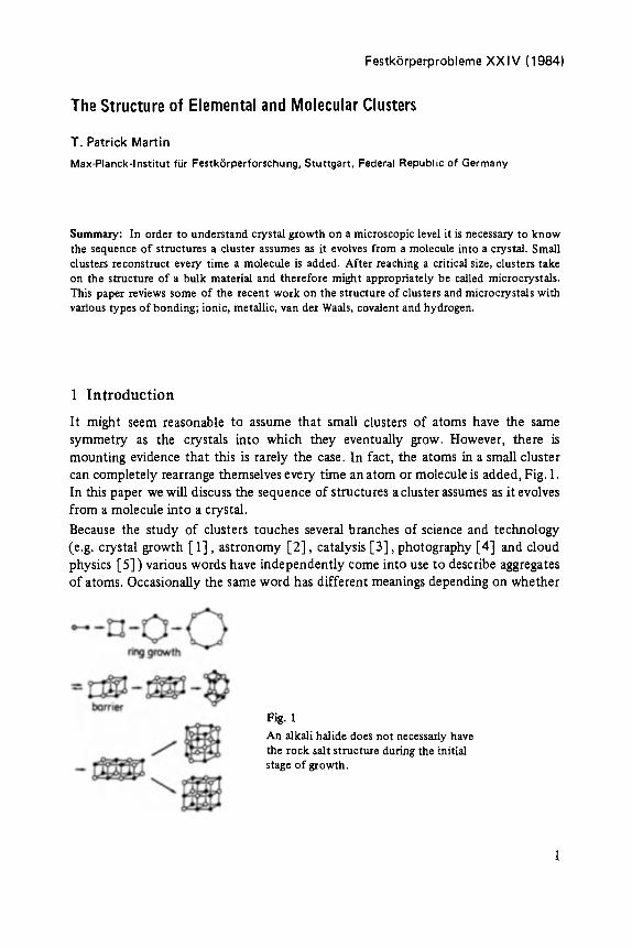
It might seem reasonable to assume that small clusters of atoms have the same symmetry as the crystals into which they eventually grow. However, there is mount ing evidence that this is rarely the case. In fact, the atoms in a small cluster
can completely rearrange themselves every t ime an atom or molecule is added, Fig. 1. In this paper we will discuss the sequence of structures a cluster assumes as it evolves from a molecule into a crystal.
Because the s tudy of clusters touches several branches of science and technology (e.g. crystal growth [ 1] , as t ronomy [ 2 ] , catalysis [3 ] , photography [4] and cloud physics [ 5]) various words have independen t ly come into use to describe aggregates of atoms. Occasionally the same word has different meanings depending on whether
Fig. 1
An alkali halide does not necessarly have the rock salt structure during the initial stage of growth.
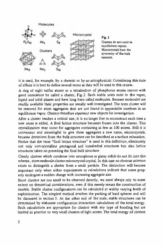
Fig. 2 Clusters do not exist in equilibrium vapors. blicrocrystals have the symmetry of the bulk material.
it is used, for example, by a chemist or by an astrophysicist. Considering this state of affairs it is best to define several terms as they will be used in this review.
A ring of eight sulfur atoms or a tetrahedron of phosphorus atoms cannot with good conscience be called a cluster, Fig. 2. Such stable units exist in the vapor, liquid and solid phases and have long been called molecules. Because molecules are readily available their properties are usually well investigated. The term cluster will be reserved for atom aggregates that are not found in appreciable numbers in an equilibrium vapor. Clusters therefore represent new objects for investigation.
After a cluster reaches a critical size, it is no longer free to reconstruct each time a new atom is added. A final lattice structure becomes frozen into the cluster. This crystallization may occur for aggregates containing as few as 100 atoms. Still it is convenient and meaningful to give these aggregates a new name, microcrystals, because deviations from the bulk structure can be described as a surface relaxation. Notice that the term "final lattice structure" is used in this definition, eliminately not only non-crystalline pentagonal and icosahedral structures but also lattice structures taken on preceding the final bulk structure.
Clearly clusters which condense into amorphous or glassy solids do not fit into this scheme, atom-molecule-cluster-microcrystal-crystal. In this case no obvious criterion exists to distinguish a cluster from a small particle. The distinction will become important only when either experiments or calculations indicate that some prop- erty undergoes a sudden change with increasing aggregate size.
Since clusters are too small to be observed directly, we must always rely to some extent on theoretical considerations, even if this merely means the construction of models. Stable cluster configurations can be calculated at widely varying levels of sophistication. The simplest method involves the packing of hard spheres and will be discussed in section 5. At the other end of the scale, stable structures can be determined by elaborate configuration interaction calculations of the total energy. Such calculations are appropriate for clusters with any type of bonding but are limited in practice to very small clusters of light atoms. The total energy o f clusters
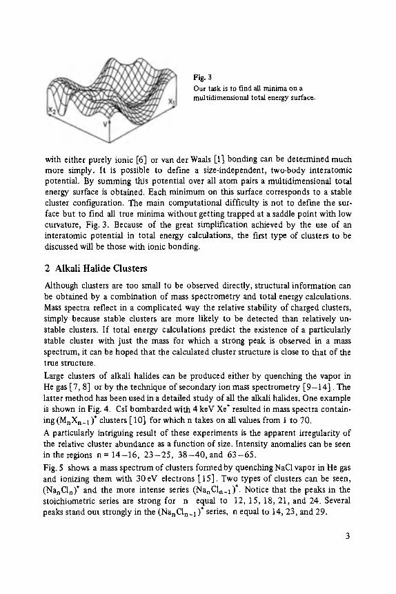
Fig. 3
Our task is to find all minima on a mult idimensional total energy surface.
with either purely ionic [6] or van der Waals [1] bonding can be determined much more simply. It is possible to define a size-independent, two-body interatomic potential. By summing this potential over all atom pairs a multidimensional total energy surface is obtained. Each minimum on this surface corresponds to a stable cluster configuration. The main computational difficulty is not to def'me the sur- face but to find all true minima without getting trapped at a saddle point with low curvature, Fig. 3. Because of the great simplification achieved by the use of an interatomic potential in total energy calculations, the first type of clusters to be discussed will be those with ionic bonding.
2 Alkali Hal ide O u s t e r s
Although clusters are too small to be observed directly, structural information can be obtained by a combination of mass spectrometry and total energy calculations. Mass spectra reflect in a complicated way the relative stability of charged clusters, simply because stable dusters are more likely to be detected than relatively un- stable clusters. If total energy calculations predict the existence of a particularly stable cluster with just the mass for which a strong peak is observed in a mass spectrum, it can be hoped that the calculated cluster structure is close to that of the true structure.
Large clusters of alkali halides can be produced either by quenching the vapor in He gas [7, 8] or by the technique of secondary ion mass spectrometry [ 9 - 1 4 ] . The latter method has been used in a detailed study of all the alkali halides. One example is shown in Fig. 4. CsI bombarded with 4 keV Xe § resulted in mass spectra contain- ing (MnXn_ 1 )+ clusters [ 10] for which n takes on all values from I to 70.
A particularly intriguing result of these experiments is the apparent irregularity of the relative cluster abundance as a function of size. Intensity anomalies can be seen in the regions n = 14-16 , 2 3 - 2 5 , 3 8 - 4 0 , and 6 3 - 6 5 .
Fig. 5 shows a mass spectrum of clusters formed by quenching NaC1 vapor in He gas and ionizing them with 30 eV electrons [ 15]. Two types of dusters can be seen, (NanCln) § and the more intense series (NanCln_l)*. Notice that the peaks in the stoichiometric series are strong for n equal to 12, 15, 18, 21, and 24. Several peaks stand out strongly in the (NanCln_l) § series, n equal to 14, 23, and 29.
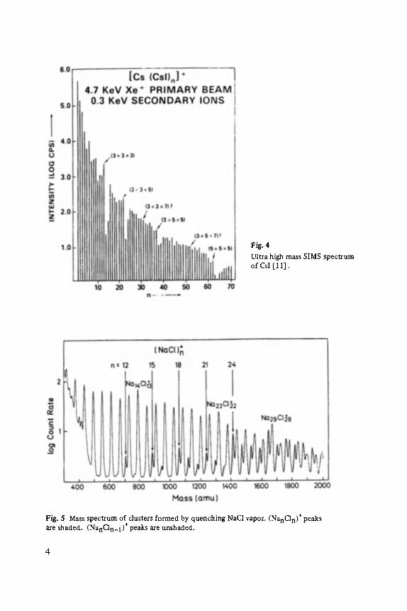
Fig. 4 Ultra high mass SIMS spectrum of CsI [11].
Fig. 5 Mass spectrum of clusters formed by quenching NaC1 vapor. (NanCln) § peaks are shaded. (NanCln_t) § peaks are unshaded.

Clusters of alkali halides observed in mass spectrometers usually do not contain equal numbers of alkali and halide atoms. This fact merely reflects the high degree of ionicity in these materials and can be explained as follows: Mass selection is possible only if a cluster is charged. If all electrons in the cluster are localized, the electrons most easily removed can be thought of as belonging to the halide ions. After ionization the neutral halide atom interacts with the remaining ions in the cluster only through a relatively weak monopole-induced dipole term. This inter- action is insufficient to compete with the large amount of energy converted to vibrational motion during the ionization process. The neutral halide atom is lost resulting in a cluster with composition (MnXn_ I )§
The intensity of a given line in a mass spectrum is influenced by many factors; the stability of the neutral clusters entering the ionization chamber, the cross section for ionization, the probability of fragmentation, and finally the stability of the ionized products. The relative stability of charged clusters having the composition (MnXn_l) § can be determined by minimizing the total energy composed of two body interactions [6, 16, 17].
Zi Z i Vij = + A exp(- rij/P ) . (1) rij
This form turns out to be surprisingly good for the alkali halides. The total energy is the sum of all two body interactions. The total energy must be minimized to find the stable configurations. The second derivatives of the total energy with respect to displacements about the stable configuration define the force constants necessary to calculate the vibrational frequencies. The calculational procedure is very simple. First, decide how many ions are to be contained in the clusters. Place these ions anywhere in space. Then allow them to move, in the calculation, under the constraint that for each move- ment the total energy must be lowered, until it is not possible to move any ion in any direction without increasing the total energy. Then a stable or at least meta- stable configuration has been found. In this way, with only two parameters A and p, we can calculate not only the shape of clusters of all sizes, but also the binding energy, the vibrational frequencies, the free energy, and the infrared absorption. The assumption made here is that A and p are independent of cluster size and shape.
Na~ C1 § has only one stable configuration, a linear molecule with a binding energy of 7.75 eV. The calculated interatomic distance is 2.4A. Na3CI~ has two stable configurations. As can be seen in Fig. 6 the linear configuration is favored by 0.5 eV over the more close-packed cluster of the same size. The most stable form of Na4CI~ is a six ring with an additional Na ion lying 2.0A above its plane. This additional ion distorts the ring into the chair form. The distances involved are too large to permit tunneling of the Na ion through the six ring. Nas CI~ has a highly symmetric planar form which turns out to be unusually stable. Adding one mole- cule, however, destroys this high stability. Two forms of the Na6Cls clusters are

Fig. 6 Stable configurations of (NanCln-1) § clusters.
shown in Fig. 6. These are highly distorted wurtzite and NaC1 lattice structures with relatively low binding energy. The most stable cluster of this size is, however, planar. The NasCI; cluster with 50.47 eV binding energy is noteworthy because it has the CsC1 crystal structure. We have shown [6] that such a structure is not possible for neutral clusters. The stable form of NagCI~ is not shown in Fig. 6. It is a double eight ring, one ring containing an additional Na ion at its center. The binding energy is 60.32 eV.
Individual strong peaks in the mass spectra apparently reflect a high stability of the corresponding cluster. The calculated total energy per molecule for the most stable form of NaC1 clusters ranging in size from 6 atoms to 32 atoms is shown in Fig. 7. The binding energy per molecule for neutral clusters is particularly large for n = 6, 9, 12, and 15. The reason for this sequence is that six-rings stacked one on the other
Fig. 7 Binding energy per molecule for the most stable forms of positively charged and neutral NaCI clusters.
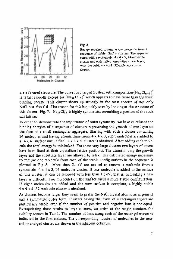
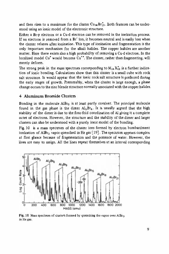
Fig. 8 Energy required to remove one molecule from a sequence of stable (NaC1) n clusters. The sequence starts with a rectangular 4 x 4 x 3, 24-molecule cluster and ends, after completing a new layer, with the cubic 4 x 4 x 4, 32-molecule cluster shown.
are a favored structure. The curve for charged clusters with composition (Na n CI n_ 1 )* is rather smooth except for (Nal, Cl13)§ which appears to have more than the usual binding energy. This cluster shows up strongly in the mass spectra of not only NaC1 but also CsI. The reason for this is quickly seen by looking at the structure of this cluster, Fig. 7. Nat4 C1~'3 is highly symmetric, resembling a portion of the rock salt lattice.
In order to demonstrate the importance of outer symmetry, we have calculated the binding energies of a sequence of clusters representing the growth of one layer on the face of a small rectangular aggregate. Starting with such a cluster containing 24 molecules and having atomic dimensions 4 x 4 x 3, eight molecules are added to a 4 x 4 surface until a f'mal 4 x 4 x 4 cluster is obtained. After adding each mole- cule the total energy is minimized. For these very large clusters two layers of atoms have been fLxed at their crystalline lattice positions. The atoms in only the growth layer and the substrate layer are allowed to relax. The calculated energy necessary to remove one molecule from each of the stable configurations in the sequence is plotted in Fig. 8. More than 3.1eV are needed to remove a molecule from a symmetric 4 x 4 x 3, 24 molecule cluster. I f one molecule is added to the surface of this cluster, it can be removed with less than 1.5 eV, that is, nucleating a new layer is difficult. Two molecules on the surface yield a more stable configuration. If eight molecules are added and the new surface is complete, a highly stable 4 x 4 x 4, 32 molecule cluster is obtained.
As clusters become larger they seem to prefer the NaC1 crystal atomic arrangement and a symmetric outer form. Ousters having the form of a rectangular solid are particularly stable even if the number of positive and negative ions is not equal. Extrapolating these results to large clusters, we arrive at the magic numbers for stability shown in Tab. 1. The number of ions along each of the rectangular axes is indicated in the first column. The corresponding number of molecules in the neu- tral or charged cluster are shown in the adjacent columns.

Table 1 Number of Molecules in Clusters with High Stability
;tructure (NaCI) n NanCl~_ 1 Structure (NaC1) n NanCl~a_ 1
3 x 3 x 1 3 x 3 x 2 3 x 3 x 3 3 x 3 x 4 3 x 3 x 5 3 x 3 x 6
9
18
27
5
14
23
4 x 4 x 2 4 x 4 x 3 4 x 4 x 4 4 x 4 x 5 3 x 3 x 7 3 x 5 x 5 5 x 5 x 4
16 24 32 40
50
32 38
3 C o p p e r Hal ide Clus ters
Bulk copper halides are usually considered to demonstrate a bonding intermediate to the ionic alkali halides and the covalent I I I - V compounds. Under moderate pressures the copper halides undergo a phase transition from the covalent zinc blende form to the ionic rock salt form. In at least one respect clusters resemble crystals under pressure: the interatomic distances are shorter. Therefore, we might except copper halide clusters to demonstrate the ionic forms calculated in the previous section.
A mass spectrum of CuBr vapor quenched in He gas is shown in Fig. 9. This spec- trum was obtained using 70 eV electrons to ionize the clusters [ 18]. Peaks due to two types of clusters can be observed in this mass spectrum, stoichiometdc CunBr~
§
clusters and fragmented CunBrn_ 1 clusters. Notice that the intensity of the peaks does not decrease monotonically with increasing cluster size but falls o f f initially
Fig. 9 Mass spectrum of cluster formed by quenching CuBr vapor. (CunBrn)+peaks are shaded. (CunBrn_l)§ unshaded.
and then rises to a maximum for the cluster Cu~4Br~3. Both features can be under- stood using an ionic model of the electronic structure.
Either a Br-p electron or a Cu-d electron can be removed in the ionization process. If an electron is removed from a B f ion, it becomes neutral and is easily lost when the cluster relaxes after ionization. This type of ionization and fragmentation is the only important mechanism for the alkali halides. The copper halides are another matter. Here there exists also a high probability of removing a Cu-d electron. In the localized model Cu § would become Cu ++. The cluster, rather than fragmenting, will merely deform.
The strong peak in the mass spectrum corresponding to M14X;3 is a further indica- tion of ionic bonding. Calculations show that this cluster is a small cube with rock salt structure. It would appear that the ionic rock salt structure is preferred during the early stages of growth. Presumably, when the cluster is large enough, a phase change occurs to the zinc blende structure normally associated with the copper halides.
4 A l u m i n u m Bromide Clusters
Bonding in the molecule A1Br3 is at least partly covalent. The principal molecule found in the gas phase is the dimer A12Br6. It is usually argued that the high stability of the dimer is due to the four-fold coordination of A1 giving it a complete octet of electrons. However, the structure and the stability of the dimer and larger clusters can also be understood with a purely ionic model of the bonding.
Fig. 10 is a mass spectrum of the cluster ions formed by electron bombardment ionization of AIBra vapor quenched in He gas [ 19]. The spectrum appears complex at first glance because of fragmentation and the presence of water. However, the lines are easy to assign. All the lines repeat themselves at an interval corresponding
Fig. 10 Mass spectrum of clusters formed by quenching the vapor over AIBr 3 in He gas.

to the mass of the A1Br3 molecule. Therefore, it is necessary to identify the lines in only one period in order to understand the complete spectrum. The lines due to [(A1Br3)n]* have been shaded. These lines are not the strongest in the spectrum. Neighboring lines are at least one order of magnitude more intense. In addition, the strength of the [(A1Br3)n] § lines do not decrease monotonically with increasing n, but alternate. The lines are weak for odd n and strong for even n.
Three lines in each period of the mass spectrum in Fig. 10 have been marked with arrows. These are due to the stoichiometric cluster ion with zero, one and two Br ions removed. A weaker line corresponding to the removal of three Br ions has not been marked explicitly. Each of these lines is in turn the first member of a series of lines separated by a mass interval of either 17 or 18 ainu, corresponding to the addition of either OH- or H20 to the cluster. The low resolution of the mass spectrometer does not allow us to distinguish betwen these two possibilities. For example, the set of lines near 1200ainu arise from the cluster AlsBrls minus two Br- ions plus zero, one and two OH- or H20 units.
The multiplicity of metastable forms of a cluster is illustrated in Fig. 11. In all cases the composition of the cluster is Ala Br12. However, through variation of the initial coordinates, seven minima have been located on the energy surface. Notice that the most stable configuration is not that with the highest symmetry or densest packing. For the configurations shown in Fig. 11, the A1 ions all lie in the same plane. We have also found shallow minima for tetrahedral arrangements of the AI ions. However, the most stable of these had less than 174 eV of binding energy.
The most stable configurations for clusters containing one to seven molecules are shown in Fig. 12. Starting with the cluster containing five molecules, a three dimen- sional arrangement of the A1 ions becomes energetically favored. The hexamer with
Fig. 11 Stable configurations of AI4BrI2 clusters. The energy for dissociation into ions is given in eV.
10
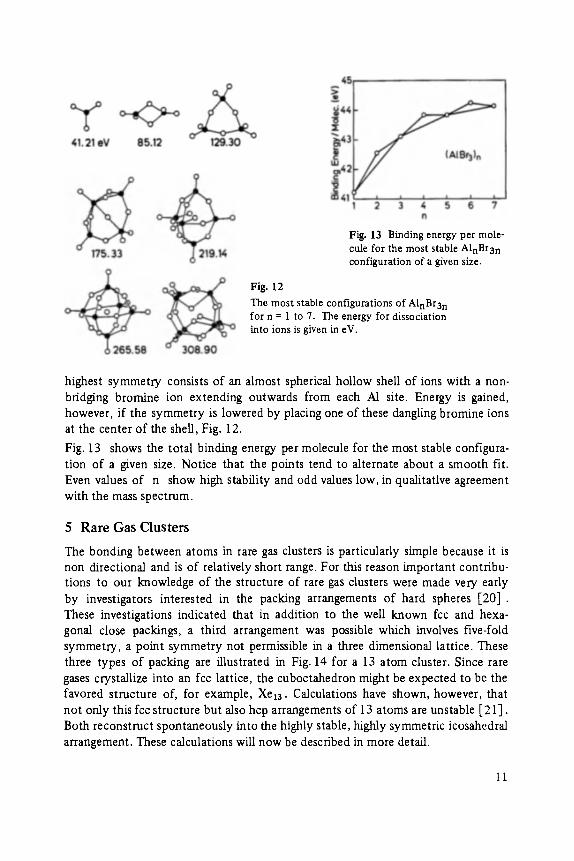
Fig. 13 Binding energy per mole- cule for the most stable AtnBr3n configuration of a given size.
Fig. 12
The most stable configurations of AlnBr3n for n = 1 to 7. The energy for dissociation into ions is given in eV.
highest symmetry consists of an almost spherical hollow shell of ions with a non- bridging bromine ion extending outwards from each A1 site. Energy is gained, however, if the symmetry is lowered by placing one of these dangling bromine ions at the center of the shell, Fig. 12.
Fig. 13 shows the total binding energy per molecule for the most stable configura- tion of a given size. Notice that the points tend to alternate about a smooth fit. Even values of n show high stability and odd values low, in qualitative agreement with the mass spectrum.
5 R a r e Gas Clus te rs
The bonding between atoms in rare gas clusters is particularly simple because it is non directional and is of relatively short range. For this reason important contribu- tions to our knowledge of the structure of rare gas clusters were made very early by investigators interested in the packing arrangements of hard spheres [20] . These investigations indicated that in addition to the well known fcc and hexa- gonal, close packings, a third arrangement was possible which involves five-fold symmetry, a point symmetry not permissible in a three dimensional lattice. These three types of packing are illustrated in Fig. 14 for a 13 atom cluster. Since rare gases crystallize into an fcc lattice, the cuboctahedron might be expected to be the favored structure of, for example, Xela. Calculations have shown, however, that not only this fcc structure but also hcp arrangements of 13 atoms are unstable [21] . Both reconstruct spontaneously into the highly stable, highly symmetric icosahedral arrangement. These calculations will now be described in more detail.
11
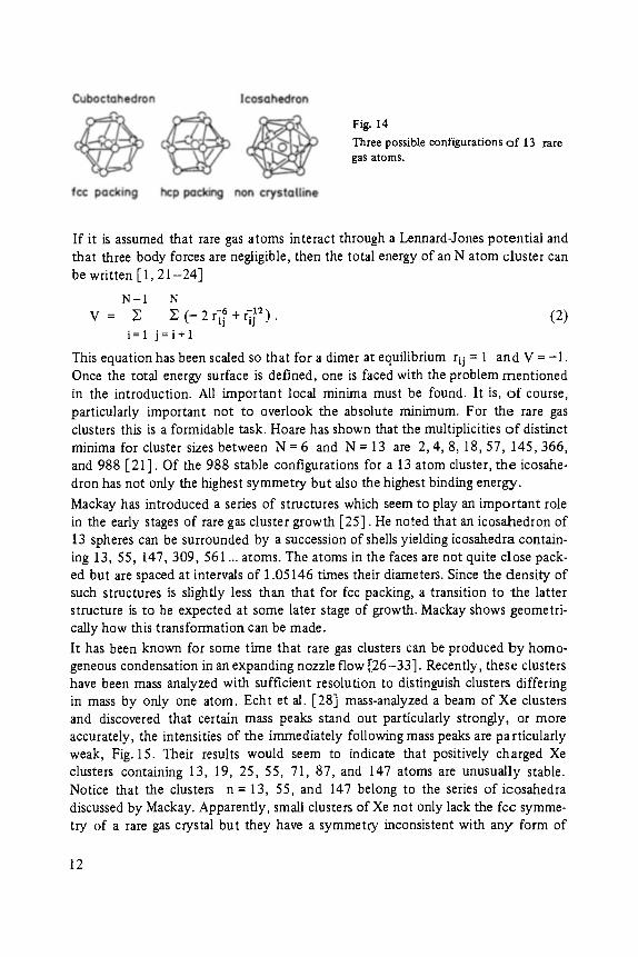
Fig. 14
Three possible configurations o f 13 rare gas atoms.
If it is assumed that rare gas atoms interact through a Lennard-Jones potential and that three body forces are negligible, then the total energy of an N atom cluster can be written [ 1 ,21-24]
N-1 N V = Z s (2)
i=l j = i + l
This equation has been scaled so that for a dimer at equilibrium rij = 1 and V = -1. Once the total energy surface is defined, one is faced with the problem mentioned in the introduction. All important local minima must be found. It is, o f course, particularly important not to overlook the absolute minimum. For the rare gas clusters this is a formidable task. Hoare has shown that the multiplicities o f distinct minima for cluster sizes between N = 6 and N = 13 are 2, 4, g, lg, 57, 145,366, and 988 [21]. Of the 988 stable configurations for a 13 atom cluster, the icosahe- dron has not only the highest symmetry but also the highest binding energy.
Mackay has introduced a series of structures which seem to play an important role in the early stages of rare gas cluster growth [25]. He noted that an icosahedron of 13 spheres can be surrounded by a succession of shells yielding icosahedra contain- ing 13, 55, 147,309, 561 ... atoms. The atoms in the faces are not quite close pack- ed but are spaced at intervals of 1.05146 times their diameters. Since the density of such structures is slightly less than that for fcc packing, a transition to the latter structure is to be expected at some later stage of growth. Mackay shows geometri- cally how this transformation can be made.
It has been known for some time that rare gas clusters can be produced by homo- geneous condensation in an expanding nozzle flow [26-33]. Recently, these clusters have been mass analyzed with sufficient resolution to distinguish clusters differing in mass by only one atom. Echt et al. [28] mass-analyzed a beam of Xe clusters and discovered that certain mass peaks stand out particularly strongly, or more accurately, the intensities of the immediately following mass peaks are particularly weak, Fig. 15. Their results would seem to indicate that positively charged Xe clusters containing 13, 19, 25, 55, 71, 87, and 147 atoms are unusually stable. Notice that the clusters n = 13, 55, and 147 belong to the series of icosahedra discussed by Mackay. Apparently, small clusters of Xe not only lack the fcc symme- try of a rare gas crystal but they have a symmetry inconsistent with any form of
12
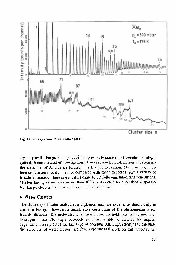
Fig. 15 Mass spectrum of Xe clusters [28].
crystal growth. Farges et al. [34, 35] had previously come to this conclusion using a quite different method of investigation. They used electron diffraction to determine the structure of Ar clusters formed in a free jet expansion. The resulting inter- ference functions could then be compared with those expected from a variety of structural models. These investigators came to the following important conclusions. Clusters having an average size less then 800 atoms demonstrate icosahedral symme- try. Larger clusters demonstrate crystalline fcc structure.
6 Water Clusters
The clustering of water molecules is a phenomenon we experience almost daily in northern Europe. However, a quantitative description of the phenomenon is ex- tremely difficult. The molecules in a water cluster are held together by means of hydrogen bonds. No single two-body potential is able to describe the angular dependent forces present for this type of bonding. Although attempts to calculate the structure of water clusters are few, experimental work on this problem has
13
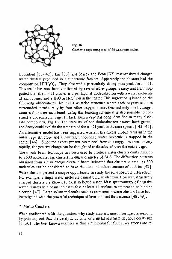
Fig. 16 Clathrate cage composed of 20 water molecules.
flourished [ 3 6 - 4 2 ] . Lin [36] and Searcy and Fenn [37] mass-analyzed charged water clusters produced in a supersonic free jet. Apparently the clusters had the composition H§ They observed a particularly strong mass peak for n = 21. This result has now been confirmed by several other groups. Searcy and Fenn sug- gested that the n = 21 cluster is a pentagonal dodecahedron with a water molecule at each comer and a H20 o r H30 § ion in the center. This suggestion is based on the following observations. Ice has a wurtzite structure where each oxygen atom is surrounded tetrahedrally by four other oxygen atoms. One and only one hydrogen atom is found on each bond. Using this bonding scheme it is also possible to con- struct a dodecahedral cage. In fact, such a cage has been identified in many clath- rate compounds, Fig. 16. The stability of the dodecahedron against both growth and decay could explain the strength of the n = 21 peak in the mass spectra [ 4 3 - 4 5 ] .
An alternative model has been suggested wherein the excess proton remains in the outer cage structure and a neutral, unbounded water molecule is trapped in the center [46]. Since the excess proton can tunnel from one oxygen to another very rapidly, the positive charge can be thought of as distributed over the entire cage.
The nozzle beam technique has been used to produce water clusters containing up to 2600 molecules i.g. clusters having a diameter of 54 A. The diffraction patterns obtained from a high energy electron beam indicated that clusters as small as 300 molecules can be considered to have the diamond cubic structure of bulk ice [42].
Water clusters present a unique opportunity to study the solvent-solute interaction. For example, a single water molecule cannot bind an electron. However, negatively charged clusters are known to exist in liquid water. Mass spectrometry o f negative water clusters in a beam indicates that at least 11 molecules are needed to bind an electron [47]. Large solute molecules such as tetracene in water clusters have been investigated with the powerful technique of laser induced fluorescence [48 ,49] .
7 Metal Clusters
When confronted with the question, why study clusters, most investigators respond by pointing out that the catalytic activity of a metal aggregate depends on its size [3, 50]. The best known example is that a minimum for four silver atoms are re-
14
quired to catalyse photographic development [51 ]. Although the potential applica- tion of metal cluster studies to the field of catalysis has stimulated a great deal of activity, it remains an exceedingly difficult branch of cluster physics with the main burden being carried by the theorists.
No meaningful two-body interaction can be defined for metal atoms which is in- dependent of cluster size and shape. We cannot escape the fact that the total energy must be calculated quantum mechanically for a many-atom problem without the benefit of translational symmetry. Semi-empirical methods (Htickel, CNDO: Com- plete Neglect of Differential Overlap [51], DIM: Diatomics-ln-Molecules [52]) are certainly important for first studies, particularly for large clusters composed of heavy atoms. If and when a large mass of structural data becomes available on metal clusters, it may be possible to develop rules for choosing model parameters making these methods even more valuable. Unfortunately, at present we are faced with a complete absence of direct structural determinations.
Other computational methods have been used over the years to calculate the total energy of small metal clusters. The relative merits of various methods is still a matter of much controversy, but some conclusions are now emerging which seem to be generally accepted. The Hartree-Fock method is not adequate. Electron Coulomb correlation, by definition not included in this method, accounts for most of the binding energy in many types of metal cluster. The Xa method, using a local spin density potential, is in principal merely an approximation to the Hartree-Fock calculation. From this point of view it could not be expected to improve the situation. However, in practice the Xa method is not only simpler to carry out but it gives much more realistic results [53, 54]. A standard is needed to check the range of validity of such calculational methods. Since experimentalists have not been able to provide that standard, one must look to calculations which explicitly include electron correlation, the most sophisticated being the configuration inter- action method [55-59] . A simpler method, involving the use of density func- tionals, has been applied to neutral and positively charged clusters containing up to eight atoms [60-62]. Comparison with the results of CI (Configuration Interaction) calculations, where possible, was good.
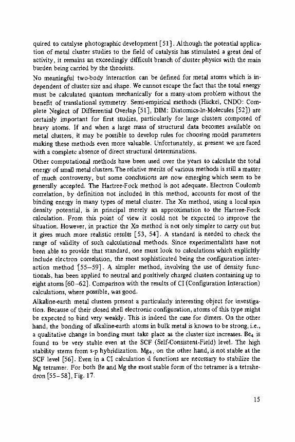
Alkaline-earth metal clusters present a particularly interesting object for investiga- tion. Because of their closed shell electronic configuration, atoms of this type might be expected to bind very weakly. This is indeed the case for dimers. On the other hand, the bonding of alkaline-earth atoms in bulk metal is known to be strong, i.e., a qualitative change in bonding must take place as the cluster size increases. Be4 is found to be very stable even at the SCF (Self-Consistent-Field) level. The high stability stems from s-p hybridization. Mg4, on the other hand, is not stable at the SCF level [56]. Even in a CI calculation d functions are necessary to stabilize the Mg tetramer. For both Be and Mg the most stable form of the tetramer is a tetrahe- dron [55-58], Fig. 17.
15

Fig. 17 Calculated stable configurations of metal dusters [55-62].
CI calculations indicate that the most stable configuration of Li4 is a rhombus [59-62], Fig. 17. Close packed, three dimensional arrangements do not demon- strate even a relative minimum in the total energy. An important lesson to be learn- ed here is that models based on sphere packing should be applied to small metal clusters only with caution.
Metal clusters have been generated in the laboratory using a number of different techniques I63 -73 ] . The bombardment of solid Li with high energy ions pro- vided an early source of Li clusters [63]. An even-odd variation in the cluster inten- sities, l(Li~n+ t) > I(Li~n ), was interpreted to indicate the higher stability of con- figurations with paired electrons. An even-odd effect was also observed for Na clusters formed by free jet expansion. However, the effect was seen not only in the mass spectrum but also in the threshold for photoionization 164]. The even-odd effect is shown in Fig. 18 for Cs clusters formed by quenching Cs vapor in a mix- ture of He and 02 gas. The additional peaks in the spectrum are due to the forma- tion of suboxides, the topic of main interest in this investigation [65].
Well defined anomalies have been observed in mass spectra of Pb clusters [66] produced by inert gas condensation, of Na clusters [67] produced by seeded beam expansion, of Ni and A1 clusters [68], formed by a high temperature oven and a
Fig. 18 Mass spectrum of clusters formed by quenching Cs vapor in a mixture of He and O2 gas.
16
quenched flow, and of A1 and Fe clusters produced by laser evaporation followed by seeded beam expansion [70]. The interpretation of these interesting spectra awaits reliable total energy calculations for large clusters.
Detailed spectroscopic information has recently been obtained on metal dimers and trimers using the techniques of resonant, two-photon ionization and laser induced fluorescence [71-73] . These experiments give us hope that in the future we will not have to be content with merely qualitative discussions of strong peaks in mass spectra. The experimental determination of ionization energies, electronic excita- tion energies, vibrational frequencies, and perhaps even rotational energies of large unsupported metal clusters may soon become a reality.
8 V-VI Clusters
Arsenic and sulfur combine to form a rich variety of compounds. As, S, (realgar) is composed of 8-atom molecules weakly bonded with one another by van der Waals forces. As2 $3 has a polymeric layer structure (orpiment). Finally, molten As-S can be quenched to form glass. One motivation for studying the relative stability of As-S clusters is the identification of other highly stable building blocks which could lead to the synthesis of new compounds. Moreover, information concerning the stability of free clusters could shed light on the structure of glass.
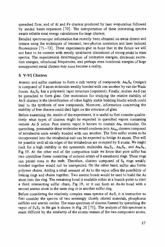
Before examining the results of the experiment, it is useful to first consider qualita- tively what types of clusters might be expected in quenched vapors containing various As:S ratios. Pure arsenic vapor is known to contain As4 molecules. On quenching, presumable these molecules would condense into AS4n clusters composed of tetrahedral units weakly bonded with one another. The first sulfur atoms to be incorporated into the tetrahedral unit can be expected to bridge As atoms. This will be possible until all six edges of the tetrahedron are occupied by S atoms. We might look for a high stability in the symmetric molecules As4S3, As4S4, and AsaS6, Fig. 19. At the other end of the compostion scale we know that pure sulfur has two crystalline forms consisting of ordered arrays of 8-membered rings. These tings can persist even in the melt. Therefore, clusters composed of Ss rings weakly bonded together would not be unexpected. On the other hand, sulfur also forms polymer chains. Adding a small amount of As to the vapor offers the possibility of linking rings and chains together. Two arsenic bonds would be used to build the As atom into the ring. The remaining bond is available either as a branch point to start a third intersecting sulfur chain, Fig. 19, or it can form an As-As bond with a second arsenic atom in the same ring or in another sulfur ring.
Before considering the relatively complex mass spectra of As-S, it is instructive to first consider the spectra of two seemingly closely related materials, phosphorus sulfides and arsenic oxides. The mass spectrum of clusters formed by quenching the vapor of P4S3 in He gas is shown in Fig. 20 [75]. The analysis of this spectrum is made difficult by the similarity of the atomic masses of the two component atoms,
17
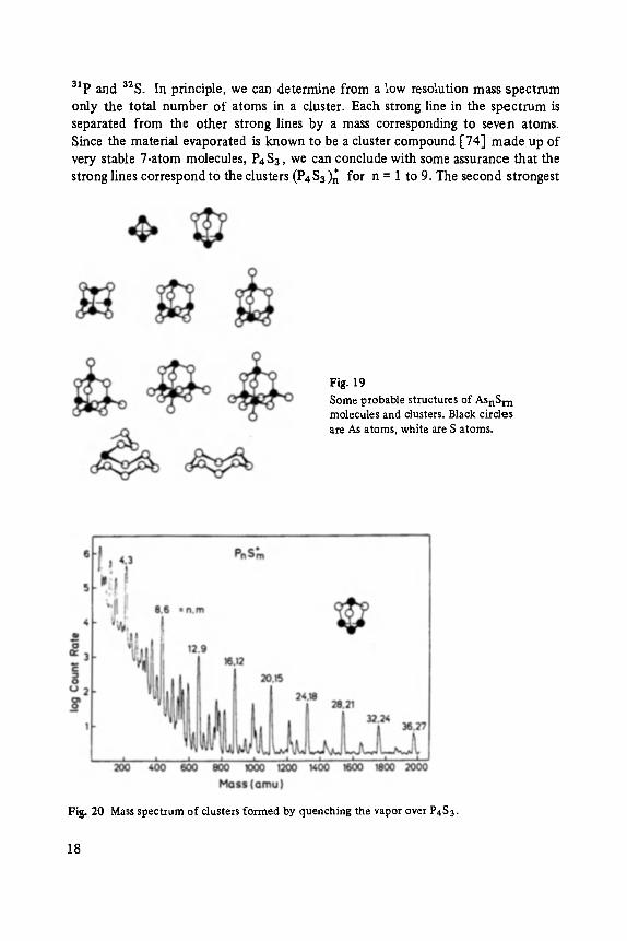
3~p and 32S. In principle, we can determine from a low resolution mass spectrum only the total number of atoms in a cluster. Each strong line in the spect rum is separated from the other strong lines by a mass corresponding to seven atoms. Since the material evaporated is known to be a cluster compound [74] made up of very stable 7-atom molecules, P4S3, we can conclude with some assurance that the strong lines correspond to the clusters (P4S3)n for n = 1 to 9. The second strongest
Fi~. 19 Some probable structures of AsnSrn molecules and dusters. Black circles are As atoms, white are S atoms.
Fig. 20 Mass spectrum of clusters formed by quenching the vapor over P4S3.
18
lines occur exactly half-way between the strongest lines and are, therefore, prob- S . § 2 4 7 ably due to the doubly ionized clusters (P4 3 ) n �9 Double ionization without frag-
mentation appears to be more probable in large clusters where the excess positive charge can occupy a greater volume thus reducing its self energy. The weaker lines correspond to the fragments (P4S3)~ minus 2, 3, 4, 5, and 6 atoms.
The most important aspect of the P-S spectrum can be seen at first glance. It is extremely simple. Essentially, singly and doubly charged clusters of only one type are observed. These clusters are constructed with P4 $3 building blocks. Presumably, these units are only weakly bonded with one another just as they are in the mole- cular crystal. This simplicity is in sharp contrast to the mass spectra of As-S, as we will show later.
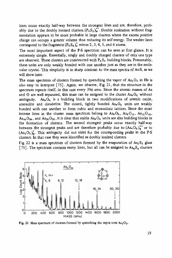
The mass spectrum of clusters formed by quenching the vapor of As2 03 in He is also easy to interpret [75]. Again, we observe, Fig. 21, that the structure in the spectrum repeats itself, in this case every 396 amu. Since the atomic masses of As and O are well separated, this mass can be assigned to the cluster As406 without ambiguity. As406 is a building block in two modifications of arsenic oxide, arsenolite and claudetite. The closed, tightly bonded AS406 units are weakly bonded with one another to form cubic and monoclinic lattices. Since the most intense lines in the cluster mass spectrum belong to As406, As8Oz2, Asz2Ozs, Asz60~, and As20030, it is clear that stable As406 units are also building blocks in the formation of clusters. The second strongest peaks occur exactly half-way
§ 2 4 7 between the strongest peaks and are therefore probably due to (As406)n or to (As203)n. This ambiguity did not exist for the corresponding peaks in the P-S clusters. In that case they were identified as doubly ionized clusters.
Fig. 22 is a mass spectrum of clusters formed by the evaporation of As2S3 glass [75]. The spectrum contains many lines, but all can be assigned to AsnS x clusters
Fig. 21 Mass spectrum of clusters formed by quenching the vapor over As203.
19
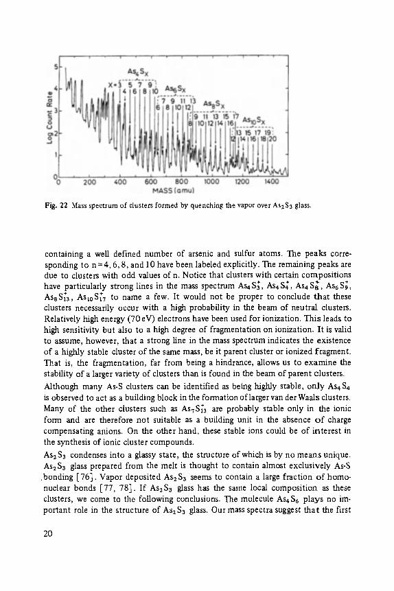
Fig. 22 Mass spectrum of clusters formed by quenching the vapor over As2S 3 glass.
containing a well defined number of arsenic and sulfur atoms. The peaks corre- sponding to n = 4, 6, 8, and 10 have been labeled explicitly. The remaining peaks are due to clusters with odd values of n. Notice that clusters with certain compositions
§ §
have particularly strong lines in the mass spectrum As4 S~, As4 $4, As4 S~, As6 $9, § §
AssS13, AsloS17 to name a few. It would not be proper to conclude that these clusters necessarily occur with a high probability in the beam of neutral clusters. Relatively high energy (70 eV) electrons have been used for ionization. This leads to high sensitivity but also to a high degree of fragmentation on ionization. I t is valid to assume, however, that a strong line in the mass spectrum indicates the existence of a highly stable cluster of the same mass, be it parent cluster or ionized fragment. That is, the fragmentation, far from being a hindrance, allows us to examine the stability of a larger variety of clusters than is found in the beam of parent clusters.
Although many As-S clusters can be identified as being highly stable, only As4 $4 is observed to act as a building block in the formation of larger van der Waals clusters. Many of the other clusters such as AsTS~3 are probably stable only in the ionic form and are therefore not suitable as a building unit in the absence o f charge compensating anions. On the other hand, these stable ions could be of interest in the synthesis of ionic cluster compounds.
As2 $3 condenses into a glassy state, the structure of which is by no means unique. As~S3 glass prepared from the melt is thought to contain almost exclusively As-S
,bonding [76]. Vapor deposited As2S3 seems to contain a large fraction o f homo- nuclear bonds [77, 78]. If As2S3 glass has the same local composition as these clusters, we come to the following conclusions. The molecule As4 $6 plays no im- portant role in the structure of As2S3 glass. Our mass spectra suggest that the first
20
stable building block with composition As2nSan is the molecule As6 $9. In addition, As-As bonding is compensated not by excess sulfur in the form of S-S bonds but by terminal sulfur atoms on 4-feld coordinated As atoms.
9 Conc lud ing R e m a r k s
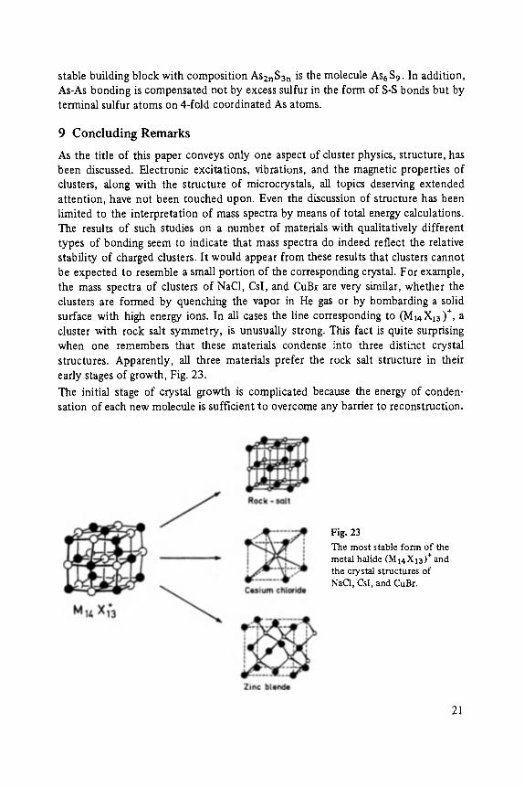
As the title of this paper conveys only one aspect of cluster physics, structure, has been discussed. Electronic excitations, vibrations, and the magnetic properties of clusters, along with the structure of microcrystals, all topics deserving extended attention, have not been touched upon. Even the discussion of structure has been limited to the interpretation of mass spectra by means of total energy calculations. The results of such studies on a number of materials with qualitatively different types of bonding seem to indicate that mass spectra do indeed reflect the relative stability of charged clusters. It would appear from these results that clusters cannot be expected to resemble a small portion of the corresponding crystal. For example, the mass spectra of clusters of NaCI, CsI, and CuBr are very similar, whether the clusters are formed by quenching the vapor in He gas or by bombarding a solid surface with high energy ions. In all cases the line corresponding to (M14X1a)*, a cluster with rock salt symmetry, is unusually strong. This fact is quite surprising when one remembers that these materials condense into three distinct crystal structures. Apparently, all three materials prefer the rock salt structure in their early stages of growth, Fig. 23.
The initial stage of crystal growth is complicated because the energy of conden- sation of each new molecule is sufficient to overcome any barrier to reconstruction.
Fig. 23 The most stable form of the metal halide (M 14Xla)+ and the crystal structures of NaC1, CsI, and CuBr.
21

For large clusters this energy is distr ibuted over so many degrees of f reedom that a characteristic structure is frozen into the cluster. Further growth takes place by the nucleation and growth of surface layers, just as in bulk crystals.
References
[1] M.R. Hoare and P. Pal, Adv. Phys. 20, 161 (1971); see articles in Proc. Int. Meeting on Small Particles and Inorganic Clusters, J. Physique, Suppl. C2 (1977), and Surface Sci. 106 (1981).
[2] P. A. Aannestad and E. M. Purcell, Ann- Rev. Astr. and Astrophys. 11, 309 (1973); D. R. Hoffmann, Adv. in Phys. 26, 129 (1977); Solid State Astrophysics, IV. C Wick. ramasinghe and D. S. Morgan, editors (D. Reidel, Publishing Company, Dordrecht- Holland, 1976).
[ 3] Growth and Properties of Metal Clusters, Applications to Catalysis and the Photographic Process. Jean Bourdon, Editor (Elvesier Scientific Publishing Company, Amsterdam, 1980).
[4] 7". H. James, ed., The Theory of the Photographic Process, 3rd ed. (The Macmillan Com- pany, New York, 1966).
[5] Conference on Cloud Physics and Atmospheric Electricity (American Meteorological Society, Boston, 1979).
[6] T.P. Martin, Physics Reports 95,167 (1983). [7] K. Sattler, in: Festk6rperprobleme (Advances in Solid State Physics), Vol. XXIII, 13,
P. Grosse (ed.), Vieweg, Braunsehweig 1983. [8] K. Sattier, Z MCihlbach, O. Eeht, 1'. P[au, and E. Recknagel, Phys. Rev. Lett. 47, 160
(1981). [9] F. Honda, G. M. Lancaster, Y. Fukuda, and S. W. Rabelais, J. Chem. Phys. 69, 4931
(1978). [10] J. Campana, T. M. Barlak, R. Z Colton, l .J . DeCorpo, Z R. Wyatt, andB. L Dunlap,
Phys. Rev. Lett. 47, 1046 (1981). Ell] T.M. Barlak, J .E. Campana, R .J . Colton, J. Z DeCorpo, a n d Z R . Wyart, J. Chem.
Phys. 85, 3840 (1981). [12] 1". M. Barlak, Z R. Wyatt, R. J. Colton, J. Z De Corpo, and I. E. Campana, J. Am.
Chem. Soc. 104, 1212 (1982). [13] T.M. Barlak, J. E. Campana, I. R. Wyatt, and R. J. Colton, J. Chem. Phys. 87, 3441
(1983). [ 14] W. Ens, R. Beauis, and K. G. Standing, Phys. Rev. Lett. 50, 27 (1983). [ 15] T.P. Martin, to be published in Bet. Bunsenges. Phys. Chem. [16] T.P. Martin, J. Chem. Phys. 67, 5207 (1977); 69, 2036 (1978); 72, 3506 (1 980). [17] D.O. Welch, O. W. Lazareth, G. J. Dienes, and R. 1). Hatcher, J. Chem. Phys. 64,835
(1976); 68, 2159 (1978). [ 18] T.P. Martin and A. Kakizaki, to be published in J. chem. Phys. [19] T.P. Martin and J. Diefenbach, J. Am. Chem. Soc. 106, 623 (1984). [20] J.D. Bernal, Nature 185, 68 (1960); Proe. Roy. Soe. A280, 299 (1964). [21] M.R. Hoare, Adv. Chem. Phys. 40, 49 (1979).
22

[22] R.-P. Pan and R. D. Etters, J. Chem. Phys. 72, 1741 (1980); E. E. Polymeropoulos and J. Brickmann, Chem. Phys. Lett. 96, 273 (1983).
[23] J.G. Allpress and J. V. Sanders, Aust. J. Phys. 23, 23 (1970). [24] J.J. Burton, J. Chem. Phys. 52, 345 (1970). [25] A.L . Mackay, Acta Cryst. 15,916 (1962). [26] E. W. Becker, K. Bier, and Ir Henkes, Z. Physik 146,333 (1956). [27] O.F. Hagena and tr Obert, J. chem. Phys. 56, 1793 (1972). [28] O. Echt, K. Sattler, and E. Recknagel, Phys. Rev. Lett. 47, 1121 (1981). [29] J. Gspann, Surf. Sci. 106,219 (1981). [30] R. G. Orth, H. T. Jonkman, D. H. Powell, and J. Michl, J. Am. Chem. Soc. 103, 6026
(1981). [31] L. Friedman and R. Z Beuhler, J. Chem. Phys. 78, 4669 (1983). [32] P. W. Stephens and J. G. King, Phys. Rev. Lett. 51, 1538 (1983). [33] A. Ding and J. Hesslich, Chem. Phys. Lett. 94, 54 (1983). [34] J. Farges, B. Raoult, and G. Torchet, J. Chem. Phys. 59, 3454 (1973). [35] J. Farges, M. F. De Feraudy, B. Raoult, and G. Torchet, Surf. Sci. 106, 95 (1981).
[36] S.-S. Lin, Rev. Sci. Instrum. 44, 576 (1973). [37] J.Q. Searcy and J. B. Fenn, J. Chem. Phys. 61, 5292 (1974). [38] G.M. Lancaster, F. Honda, Y. Fukuda, and J. Ir Rabalais, J. Am. Chem. Soc. 101,
1951 (1979).
[39] D. Dreyfuss and H. Y. lCachman, J. chem. Phys. 76, 2031 (1982). [40] R.J. Beuhler and L. Friedman, J. Chem. Phys. 77, 2549 (1982). [41] A. Z Stace and C. Moore, Chem. Phys. Lett. 96, 80 (1983). [42] G.D. Stein and J. A. Armstrong, J. Chem. Phys. 58, 1999 (1973). [43] B. iV. Hale and P. L. M. Plummet, J. Atmos. Sci. 3t, 1615 (1974). [44] J.L. Kassner, Jr. and D. E. Hagen, J. Chem. Phys. 64, 1860 (1976). [45] F.H. Stillinger and C. PC. David, J. Chem. Phys. 73, 3384 (1980). [46] P.M. Holland and A. W. Castleman, Jr., J. Chem. Phys. 72, 5984 (1980). [47] H. Haberland, H. Langosch, E..G. Schindler, and D. R. Worsnop, to be published in Ber.
Bunsenges. Phys. Chem. [48] U. Even and Z Jortner, J. Chem. Phys. 78, 3445 (1983). [49] A. Z Stace and C. Moore, J. Chem. Phys. 19, 3681 (1983). [50] J. M. Dartigues, A. Chambellan, and F. G. Gault, J. Am. Chem Soc. 98, 856 (1976). [51] R.C. Baetzold and J. F. Hamilton, Prog. Solid St. Chem. 15, 1 (1983). [52] S. C. Richtsmeier, M. L. Hendewerk, D. A. Dixon, and J. L. Gole, J. Phys. Chem. 86,
3932 (1982). [53] 19. R. Salahub, NATO ASI - Impact of Cluster Physics in Materials Science and Tech-
nology, J:. Davenas, ed., Nijhoff, The Hague, 1983. [54] D.R. Salahub and R. P. Messmer, Phys. Rev. B16, 2526 (1977).
[55] R.A . Chiles, C. E. Dykstra, and K. D. Jordan, J. Chem. Phys. 75, 1044 (1981). [56] C. W. Bauschlicher, Jr., P.S. Bagus, andB. N. Cox, J. Chem. Phys. 77,4032(1982).
[57] G. Pacchioni and Z Koutecky, Chem. Phys. 71,181 (1982). [58] G. Pacchioni and J. Koutecky, J. Chem. Phys. 77, 5850 (1982).
23
[59] D. Plavsic, J. Koutecky, G. Pacchioni, and V. Bonacic-Koutecky, J. Phys. Chem. 87, 1096 (1983); P. Fantucci, J. Koutecky, and G. Pacchioni, to be published in J. Phys. Chem.
[60] R. O. Jones, J. Chem. Phys. 71, 1300 (1979); Z Harris and R. O. Jones, J. Chem. Phys. 68, 1190 (1978).
[61] J. Flad. H. Stoll, and tt. Preuss, J. Chem. Phys. 71, 3042 (1979); Z Flad, G. 1gel, M. Dolg, 1-1. Stoll, and H. Preuss, Chem. Phys. 75, 331 (1983); M. P. lniguez, C. Bala- dron, andJ. A. Alonso, Surf. Sci. 127, 367 (1983).
[62] R. Car and J. L. Martins, Surf. Sci. 106,280 (1981).
[63] M. Leleyter and P. Joyes, J. Physique 36, 343 (1975); J. Physique, Suppl. C2, 11 (1977).
[64] A. Herrnann, S. Leutwyler, E. Schumacher, and L. tr Heir. Chim. Acta 61,452 (1978); A. Hoareau, B. Cabaud, andP. Melinon, Surf. Sci. 106,195 (1981).
[65] T.P. Martin and J. Diefenbach, to be published.
[66] K. Sattler, J. Mahlbach, and E. Recknagel, Phys. Rev. Lett. 45, 82I (1980).
[67] M. M. Kappes, R. Ir Kunz, and E. Schumacher, Chem. Phys. Lett. 91,413 (1982).
[68] S.J. Riley, E. K. Parks, C.-R. Mao, L. G. Pobo, and S. IVexler, J. Phys. Chem. 86, 3911 (1982).
[69] K. Kirnoto and L Nishida, J. Phys. Soc. Japan 42, 2071 (1977).
[70] T. G. Dietz, M .A . Duncan, D.E. Powers, andR. E. Smalley, J. Chem. phys. 74,6511 (1981); E. A. Rohlfing, D. M. Cox, and A. Kaldor, Chem. Phys. Lett. 99, 161 (1983).
[71] V.E. Bondybey and J. H. English, J. Chem. Phys. 74, 6978 (1981); 76, 2165 (1982). [72] J.H. Gole, G.J. Green, S.A. Pace, andD. R. Preuss, J. Chem. Phys. 76, 2247 (1982).
[73] J. B. Hopkins, P. R. R. Langridge-Smith. M. D. Morse, and R. E. Smalley, J. Chem. Phys. 78, 1627 (1983).
[74] For an interesting discussion of phosphorus containing dusters see, [1. G. von Schnering, "Catenation of Phosphorus Atoms" in: Homoatom/e Rings and Chains, edited by A. L. Rheingold (Elsevier, New York, 1977).
[75] T.P. Martin, Solid State Comm. 47, 111 (1983); J. Chem. Phys. 80, 170 (1984).
[76] A.J. Apling, A.J. Leadbetter, and A. C. Wright, J. Non-Crystalline Solids 23,369 (1977).
[77] M. F. Daniel, A. Z Leadbetter, A. C. Wright, and R. N. Sinclair, J. Non-Crystalline Solids 32, 271 (1979).
[78] R.J . Nemanich, G. A. N. Connell, T. M. Hayes, and R. A. Street, Phys. Rev. B18, 6900 (1978).
24
Festk6rperproblerne XXlV (1984)
The Fractional Quantum Hall Effect
Horst L. St6rmer AT & T Bell Laboratories Murray Hill, New Jersey, USA
Summary: The Fractional Quantum Hall Effect (FQHE) represents a very surprising recent discovery in solid state physics. It is observed in high-mobility, two-dimensional electron systems at low temperatures (~ 1 K) in intense perpendicular magnetic fields (-~ 200 kG) when all carriers are confined to the lowest Landau level. Under those exceptional conditions, and at fractional filling ~ of this level, the Hall resistance is found to be quantized to Pxy = h/ie 2, where i is a simple rational fraction. Concomitantly, the resistivity Pxx drops towards zero. So far this effect has been observed close to v = 1/3, 2/3, 4/3, 5/3, 2/5, 3/5, 4/5, and 2/7 with quantum numbers i = v quantized, in some cases, to better than 1 part in 10 4. The FQHE re- presents the unambiguous, experimental observation of a fractional quantum number. It is presently being explained as resulting from the formation of a novel incompressible quantum liquid with fractionally charged quasi-particles, and a finite gap separating the ground state from its excitations.
1 I n t r o d u c t i o n
For a long time, the ground state of an electron system in the extreme quantum
limit has attracted the interest of theorists and spurred challenging research efforts by experimentalists. The exceptional situation arises when a degenerate electron system is exposed to an intense magnetic field B and all carriers of density n can be accommodated in the lowest of the magnetic quantum levels (Landau levels). The stark singularities in the density of states associated with the Landau levels lead to a strong compression of the Fermi energy E F and, hence, to vanishing kinetic energy of the carriers. Under such extraordinary circumstances the Coulomb energy be-
tween particles E c ~ n 1/3 e 2/e can far exceed their average kinetic energy E k ~ EF and the generally employed independent electron picture ceases to be valid. As a result, a highly correlated carrier motion is to be expected and possibly a condensa- tion into a new electronic ground state.
Most attractive is the situation of a two-dimensional electron system in a strong perpendicular magnetic field. Its two-dimensionality assures quenching of the kinetic energy along the field direction (z) while the Landau quantization quenches the kinetic energy of the x - y motion. The carriers of an ideal two-dimensional
electron system in the extreme quantum limit have no kinetic energy, hence, carrier- carrier interaction will always dominate at low T.
25

A Wigner solid [1-3] appears to be a strong contender for the correlated ground state: the electrons form a regular lattice, with probably hexagonal symmetry. An analogy is drawn to the crystallization of a classical electron gas on the surface of liquid helium in the absence of a magnetic field [4]. The intense magnetic field imposed onto the degenerate 2D system can be regarded as to localize the carriers and, hence, the system is expected to follow the route of the classical electron gas.
These theoretical notions were brought to test in two-dimensional inversion layers at the Si-SiO2 interface of MOSFET's (Metal-oxide-semiconductor field effect transistor). Magneto-conductivity measurements revealed structures and electric field dependencies [5, 6] which could not be explained by the independent electron model [7]. Anomalies in the cyclotron resonance line shape [8] and position [9] in the quantum limit seemed to be best understood in terms of the formation of a pinned charge density wave (CDW) [10]. However, in the range of electron densities at which these experiments were performed, localization due to disorder at the Si- SiO2 interface is known to be important even in the absence of a magnetic field and consequently it has not been possible to discern true Coulomb effects from those due to disorder.
More recently, novel two-dimensional systems have been developed with much improved interfacial quality. They are termed modulation-doped heterojunction interfaces and are most commonly realized using a GaAs-(AIGa)As materials com- bination [11, 12]. These high-mobility 2D carrier systems are ideally suited to investigate experimentally the behavior of an electronic system in the extreme quantum limit.
Magneto-resistance and Hall-resistance measurements conducted over the past two years on a variety of low-density modulation-doped GaAs-(A1Ga)As heterojunc- tions at temperatures below 1 K and at magnetic fields up to 280 kG have revealed a remarkably rich pattern for the extreme quantum limit [13-17]: Quantization of the Hall resistance to exact rational fractions of h/e 2 has been observed at fractional f'filing of the lowest Landau level. Concomitant with these new plateaus, the magneto-resistance of the specimen dropped to vanishing values. These features of the magneto-transport coefficient are reminiscent of the Normal Quantum Hall Effect [18, 19] at higher temperatures and at integer values of Landau level f'xlling.
As it is now well established, the Normal Quantum Hall Effect arises from gaps in the single particle density of states between Landau level and the localization of carriers in the gap region [20-23]. In interpreting the striking results at fractional Landau level filling one, hence, is led to draw an analogy to the Normal Quantum Hall Effect and conclude that a new kind of gap, of many-particle origin, appears at fractional occupation of Landau levels. Recent theoretical calculations strongly support this notion and predict the existence of a novel electronic state, an electron liquid, at rational fractions of Landau level Filling [24, 25]. This new electronic state has remarkable properties like fractionally charged quasi-particles and resistance- less conduction at T = O. According to these theories, the earlier expected Wigner
26
solid occurs only at very low Landau level filling when the electron liquid crystallizes into the solid.
Here, we would like to review the present status of the experiment. After intro- ducing modulation-doping and describing "state-of-the-art" 2D systems, we turn shortly to the Normal Quantum Hall Effect as it can be observed in such hetero- structure systems. The major part of the review describes the experimental results on the Fractional Quantum Hall Effect. We will then briefly summarize its present understanding.
2 Modulation-Doped Heterostructures
Modulation-doping is a doping technique for semiconductor heterojunctions which spatially separates mobile carriers from their parent ionized impurities [11, 12]. This separation drastically reduces ionized impurity scattering and consequently leads to unprecedentedly high carrier mobilities. Modulation-doping can be applied to many heterostructure systems. The GaAs-(A1Ga)As system grown via Molecular Beam Epitaxy (MBE)[26] has proved to be the most successful system with electron mobilities beyond 106 cm2/Vsec [27-29]. More than a decade of MBE growth experience with this material combination, an almost perfect lattice match between its constituents, hence, an undetectable amount of interface misfit dislocations, and the fact that the carriers reside at the GaAs-side of the interface, thereby avoiding random alloy scattering, are the major reasons for its success.
Modulation-doping of a suitable heterojunction introduces dopant impurities ex- clusively into the wide band gap material in the vicinity of the interface while the narrow band gap material remains free from intentional doping, see Fig. 1. Carriers in the neighborhood of the heterojunction transfer from the dopant across the interface to the low lying band edge states of the narrow band gap material. They become bound to a narrow, approximately 100 A, wide, quasi-triangular potential well established by the interface and the Coulomb potential of the parent ionized impurities. The energy spectrum for perpendicular motion is discrete while the motion along the interface is free-electron like with an effective mass close to the band edge mass of the host semiconductor. The electronic conditions at the heterojunction are similar to those at the Si-SiO2 interface of a MOSFET [30]. The wide band gap material [generally (AlGa)As] replaces the SiO2 and the narrow band gap material [generally GaAs] replaces the Si substrate.
The advantages of the heterojunction system as compared to the MOSFET regarding transport properties are mostly due to the fact that in the MOSFET the 2D system resides at the interface between a crystalline semiconductor and a random glass while the heterojunction system provides a nearly perfectly lattice-matched semi- conductor]semiconductor interface. An earlier drawback of the modulation-doped structures, namely that its carrier concentration was established during growth and could not be varied thereafter, was recently overcome. Metal electrodes [31 ] evapo- rated on the top of the heterojunction system or simply glued to the substrate side
27
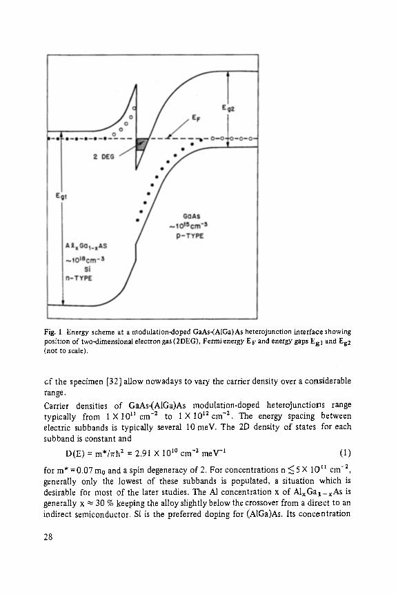
Fig. 1 Energy scheme at a modulation-doped GaAs-(AIGa)As heterojunction interface showing position of two-dimensional electron gas (2DEG), Fermi energy E F and energy gaps Egl and Eg 2 (not to scale).
cf the specimen [32] allow nowadays to vary the cartier density over a considerable range.
Carrier densities of GaAs-(A1Ga)As modulation-doped heterojunctions range typically from 1 • 1011 cm -2 to 1 X 1012 cm -2. The energy spacing between electric subbands is typically several 10 meV. The 2D density of states for each subband is constant and
D(E) = m*/nh 2 = 2.91 • 10 l~ cm -2 meV=: (1)
for m* = 0.07 m0 and a spin degeneracy of 2. For concentrations n <~ 5 • 1011 cm- : , generally only the lowest of these subbands is populated, a situation which is desirable for most of the later studies. The A1 concentration x of AlxGal_xAS is generally x ~ 30 % keeping the alloy slightly below the crossover from a direct to an indirect semiconductor. Si is the preferred doping for (AlGa)As. Its concentration
28
is typically 1 X 101 n cm -3. The fact that Si forms a deep center in Alo. 3 Gao. 7As with a binding energy of ED ~ 150 meV [27, 33] leads to a freeze out of the carriers in the (AlGa)As. This excludes undesirable conductivity in the bulk (AlGa)As in parallel to the 2D system. Mobilities (t~) in modulation-doped GaAs-(A1Ga)As range presently from typically 2 • l0 s to 1 • 106 cm2/Vsec.
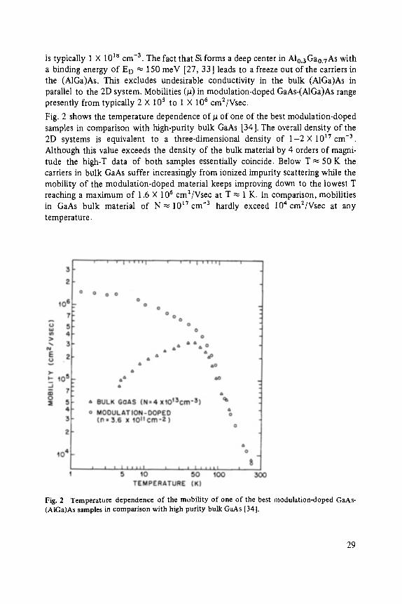
Fig. 2 shows the temperature dependence of/1 of one of the best modulation-doped samples in comparison with high-purity bulk GaAs [34]. The overall density of the 2D systems is equivalent to a three-dimensional density of 1-2 • 10 ~7 cm -3. Although this value exceeds the density of the bulk material by 4 orders of magni- tude the high-T data of both samples essentially coincide. Below T ~ 50 K the carriers in bulk GaAs suffer increasingly from ionized impurity scattering while the mobility of the modulation-doped material keeps improving down to the lowest T reaching a maximum of 1.6 X 106 cm2/Vsec at T ~ 1 K. In comparison, mobilities in GaAs bulk material of N ~ 10 t7 cm -3 hardly exceed 104 cm2/Vsec at any temperature.
Fig. 2 Temperature dependence of the mobility of one of the best modulation-doped GaAs- (AlGa)As samples in comparison with high purity bulk GaAs [341.
29

Modulation-doping is mostly employed to fabricate 2D electron systems. However, the same technique can be used to generate high-mobility 2D hole systems. This was recently demonstrated, again for the GaAs-(A1Ga)As system [35, 36]. Instead of doping -the (AIGa)As layer with the donor Si, the acceptor Be is used in MBE. The energetic conditions of the heterojunction interface are completely analogous to the n-type case except that the energy scale is inverted. Low temperature mo- bilities beyond 4 X 104 cm-2/Vsec have been achieved in this structure. With a mass-ratio of approximately 8 between hole and electron masses one finds that the scattering r of the 2D hole systems equals r of 2D electron systems with ~t
3 • l0 s.c_m_-2/Vsec. The electrical subband structure and the in-plane effective masses of these 2D hole systems are rather complex due to the existence of light and heavy holes and due to a spin-splitting induced by the absence at inversion symmetry of the heterojunction interface [37].
In concluding this section, we summarize that the modulation-doped GaAs-(A1Ga)As heterostructure is presently the two-dimensional degenerate carier system with the lowest scattering rate (r e = 6 X 10 -H sec for /~e = 1.6 X 106 cm-2/Vsec). It is therefore ideally suited to investigate the intrinsic properties of a two-dimen- sional system in the extreme quantum limit.
3 N o r m a l Q u a n t u m Hall E f f ec t (NQHE) in Modu la t i on -Doped S y s t e m s
This chapter describes some aspects of the Normal Quantum Hall Effect (NQHE) as it is observed in modulation-doped GaAs-(A1Ga)As and thereby introduces the notation used in section 4. It cannot do justice to the diversity of this rapidly expanding field. For more detailed studies we refer to a number of recent review articles [38-40]. The following section rather reminds the reader of the basic ex- perimental facts and presents an outline of their present understanding. An ex- posure to the NQHE is necessary to appreciate the lines of thought which lead to the conclusion of the existence of a new electronic ground state from the observa- tion of fractional quantization of the transport coefficients in the quantum limit.
Though the NQHE was first discovered in a Si-MOSFET [18] most of the present studies are conducted on modulation-doped heterojunctions [19, 41-46]. A smaller effective electron mass m* ~ 0.07 mo in GaAs as compared to m* ~ 0. ]q mo in Si results for similar magnetic fields B in a wider Landau level splitting
h~oc = heB/m* (2)
and, hence, in less stringent condition on the temperature kT ~ h~o c.
Fig. 3 shows one of the most distinct manifestations of the NQHE in a GaAs- (AlGa)As heterostructure at 50 mK [41]. The sample configuration is shown as an insert. Two characteristic voltages V H and V L are measured as a current I is imposed onto the 2D system and the perpendicular magnetic field B is swept up. VH, the Hall voltage across the current path, and V L, the longitudinal voltage along the
30
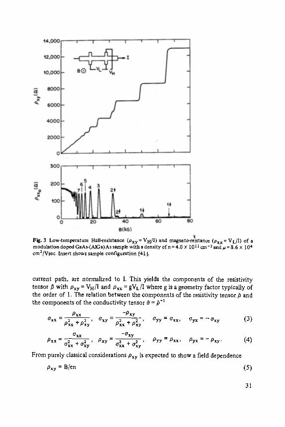
Fig. 3 Low-temperature Hall-resistance (Pxy = VH/I) and magneto-reistance (Pxx = VL/I) o f a modulat ion do pea GaAs-(A1Ga) As sample with a densi ty o f n = 4.0 • 1011 cm- 2 and ~ = 8.6 X 104 cm2lVsec. Insert shows sample configurat ion [41 ].
current path, are normalized to I. This yields the components of the resistivity tensor ~ with Pxy = VH/I and Pxx = gVL/I where g is a geometry factor typically of the order of 1. The relation between the components of the resistivity tensor ~ and the components of the conductivity tensor ~ = ~-x
Pxx - P x y O'xx - 2 2 , O'xy = 2 2 , O'yy = O'xx , O'y x = - -Oxy (3 )
Pxx § Pxy Pxx + P xy
0'xx - G x y P x x - 2 2 , Pxy = 2 + 2 ' PYY = Pxx , Pyx = - p x y . ( 4 )
Oxx + 0'xy 0"xx Oxy
From purely classical considerations Pxy is expected to show a field dependence
Pxy = B/en (5)
31
with n being the 2D electron density. Rather than this linear B-dependence, Fig. 3 shows a Hall resistivity Pxy which assumes a staircase-like structure with plateaus quantized to
#xy =h / ie 2, i = 1 , 2 , 3 . . . (6)
The accuracy of this quantization has been verified [42] to approximately 1 part in 107 . Concomitant with the appearance of plateaus in #xy, the diagonal resistivity #xx seems to vanish over large portions of B seemingly assuming f'mite values only at fields corresponding to the transition from one step to the next o f the staircase
in Pxy. Resistivities as low as Pxx < 10-1~ f2/I-1 equivalent to roughly 10 -le ~ c m , have recently been established [47]. Following the present understanding of the NQHE the formation of plateaus in Oxr and vanishing values of Oxx are directly related to the singularities in the density of states (DOS) of a 2D system in a strong perpendicular magnetic field. The DOS of an ideal two-dimensional system consists of spin-split Landau levels with energies
E = (j + 1/2) hC~c, j = 0, 1, 2 . . . + Sg*gtBB, (7)
taking the bot tom of the electric subband as the origin of E. S is the spin of the carriers, g* their effective g-factor and #B = eh/2mo is Bohr's magneton. For our purposes it is not important to discern between Landau level splitting and spin- splitting. We only retain a sequence of singularities (from now on called magnetic levels or levels) numbered by i = 1, 2, 3 ... starting with i = 1 at the lowest energy. The number of states per level for arty 2D-sysfem is
d = B/G0 = 2.42 • 10 9 cm- : kG -1 X B (8)
which is independent of any material parameter. G0 = h/e is the magnetic flux quantum. From this one can def'me a filling factor
v = n/d. (9)
At low temperatures (kT ,~ l~co c, g*/aBB) and at any given field, v indicates the num- ber of populated levels. For a system with fixed carrier density, the filling factor decreases as B is raised. The variation of the Fermi level E F is periodically abrupt due to the strongly singular DOS. At any given field, E~ resides in the close vicinity of level i = int(v) + 1. However, an exceptional situation arises at fields
B i = nq~o/i (10)
where an exact multiple i of levels is filled. Then E F is intermittant and lies in the gap region between level i and level i + 1.
The value of Pxy and the vanishing of Pxx can then be derived apparent ly in the following way: The diagonal conductivity Zxx is entirely dependent on the DOS at the position of E F. Since the DOS vanishes in the gap region, Crxx vanishes as well
32
and with Eq. 4 we derive Pxx = 0 as long as Pxy ~ 0. The classical expression Pxy = B/en holds also for quantum mechanical free electrons [40]. Hence, at a sequence of singular points on the field axis B i = n~o/i where Pxx vanishes, the Hall resistance is Pxy = q~o/ie = h/ie 2 .
Such a derivation of Pxx and Pxy neither accounts for the f'mite width of the plateaus nor for the width of the zero resistance regions both of which are the truly outstanding features of the NQHE. Explanation of a f'mite width of these features requires the existence of localized states. Localized states are expected to be present in real two-dimensional systems due to disorder as a result of random distri- bution of impurities or random interface steps. They lift the degeneracies of the magnetic levels and broaden them [48]. States at the center of this distribution will be extended while those in its tails will be localized not participating in electronic transport. (At some finite temperature, transport due to hopping among localized states will become important). This broadening of the magnetic levels moderates the abrupt jumps of EI~ from one level to the next as B is varied about the crucial values B i. Hence, for finite ranges of field, E F moves through regions of localized states between magnetic levels. In an elegant gedanken experiment, Laughlin has shown that under these conditions Pxy remains quantized and Pxx tends towards zero in spite of the disorder [22]. He demonstrates quite generally that independent of the strength of the disorder
axx=O and axy =ie /~o =ie 2/h, i = 0 , + I , - + 2 . . . (11)
whenever E~ lies within localized states (mobility gap) or within the region of a true gap. The value of i may be zero which describes the case of an insulator. Except for this degenerate case i is finite and, hence, with Eq. 4
Pxx = 0 and Pxy =h/ie2, i = 0 , • 1 7 7 (12)
which are the quantities one generally determines in transport measurements. The quantized region may be wide (as wide as 95 % plateaus and 5 % transitions [41]) indicating that the major part of the DOS consists of localized states and still Eq. 11 holds. Laughlin's gedanken experiment does not specify the value of i. For weak dis- order i is expected to coincide with the value obtained from the ideal case, in agree- ment with the experiment. Nevertheless, in general, i can considerably deviate from its unperturbed value. This fact was convincingly demonstrated for the case of addi- tional periodic potentials where dramatic variations of i can occur as the Fermi level moves through minigaps formed within the magnetic levels [49 ]. In all cases i must be an integer, though it may be negative or zero.
We summarize this chapter stating that the NQHE is understood in terms of gaps in the single particle DOS of a 2D electron syste m in a strong perpendicular magnetic field. Disorder leads to the formation of localized states in the gap region between magnetic level. Whenever the Fermi energy lies in this range Pxx = 0 and Pxy = h/ie2 (i = • 1, -+ 2 ...) excluding the degenerate case i = 0 of an insulator. A single electron picture is sufficient for a description of the NQHE.
33
4 T h e F rac t iona l Q u a n t u m Hall E f f e c t ( F Q H E )
4.1 Experimental Observation
The possible existence of a highly correlated state in a 2D electron system in the extreme quantum limit and the availability of modulation-doped heterostructures with unprecedently low amounts of disorder led to the magneto-transport studies on GaAs-(A1Ga)As structures at low temperatures in extremely high magnetic fields (up to 280 kG). In terms of the filling factor, v = n/d, the extreme quantum limit, where only the lower spin level of the lowest Landau level contains carriers, is characterized by v ~< 1.
Figs. 4 and 5 show Pxx and Pxy data for a sample with a constant electron density of n = 1.48 • 1011 cm -2 and a mobility ~ = 4.5 • 104 cm2/Vsec. For this low con- centration, exact multiples (v = i) of magnetic levels are f'filed at fields B i = nh/ie = = 61.1 kG, 30.5 kG, 20.4 kG . . . . In the vicinity of these field positions one expects the appearance of the NQHE in Pxy, accompanied by a zero resistance state in Pxx- Already at 4.2 K, the data of Figs. 4 and 5 give clear evidence of such a behavior. At even v, the Fermi level resides between Landau levels, while at odd v its posi- tion is between spin levels. The observation that the "odd structures" lag behind in development, as compared to the "even structures" reflects the fact that g*/~B B ~ hco c
Fig. 4
Magnetic field d~pendence of Pxx at T = 4.2, 0.88, and 0.14 K [16].
34
Fig. 5 Magnetic field dependence of Pxy at T = 4.2, 0.88, and 0.14 K I16].
in GaAs [50]. For B 1> B1 = 61.1 kG the filling factor v ~ 1 and, hence, the elec- tron system is in the extreme quantum limit. No prominent structures are observed neither in Oxy nor in Pxx at 4.2 K in this field region. Instead, the field dependence of Pxy reproduces quite faithfully the classical expression of Eq. 5. As T is lowered to 0.88 K, the structures due to the NQHE at v = 1 and v = 2 become fully de- veloped. Pxx spreads into wide zero resistance states while Pxy shows flat plateaus quantized to Pxy = h/ie2 , (i -- 1 ,2 ...).
35
Already at this temperature, features surprisingly appear in Pxx in the field region of the extreme quantum limit. The positions of the minima correspond closely to filling factors v = 1/3 and v = 2/3. As the temperature is lowered to 0.14 K, these structures strengthen and concomitantly features appear in Pxy. At this stage, the irregularities in the vicinity of v = 1/3 have developed into a clear zero-resistance
_ 1 2 state in Pxx with Pxx < 0.5 f2/O and a flat plateau in Pxy quantized to Pxy - h/~ e to better than one part in 104. The structures at v = 2/3 lag behind in development but must be expected to follow the same course as those around v = 1/3 as T is lowered further [14]. While the existence of plateaus in Pxy and vanishing resist- ance in Pxx at integer filling factor v are well accounted for by the NQHE the ap- pearance of similar phenomena at fractional v is inconsistent with such an inter- pretation. Not only do these structures appear at fractional occupation of a magnetic level but, moreover, Pxy is quantized to Pxy = h/ie2 with i being an exact rational fraction and not an integer.
Since phenomenologically these novel features resemble those of the NQHE, this new quantum phenomenon is termed, the Fractional Quantum Hall Effect (FQHE), though both must be of different origin. While the NQHE can be explained in terms of non-interaction 2D electrons in a high magnetic field, no such interpretation seems to be possible for the FQHE.
4.2 Phenomenologieal Interpretation of the FQHE
In order to access the possible origin of the FQHE, we return to Laughlin's ge- danken experiment described in section 3. From Pxx ~ 0 and Pxy :~ 0 at v ~ 1/3, we can deduce Oxx -~ 0. Hence, the DOS at the position of E F for partial filling of the lowest magnetic level is vanishingly low, being either zero and forming a true gap, or finite but localized, forming a mobility gap. The appearance of such gaps in the single particle DOS of 2D electrons in the extreme quantum limit, is totally unexpected. However, a 2D periodic potential in the plane of the electron motion was shown to subdivide the magnetic levels, opening new gaps in the DOS at magnetic fields where the number of f lux quanta (qSo) per unit cell is a rational fraction [49]. The existence of such periodic poten- tials within our specimen cannot be excluded a priori. A slight tilt o f the GaAs- (AlGa)As interface with respect to the (100)-axis, could produce a periodicity in 2D with the required periods [51 ]. However, the fact that e.g. the v = i /3 minimum is observed in many different samples, seems to exclude such an interpretation of our results. (This picture can be rejected also on other grounds; see further down.)
Since a description of the minima Pxx cannot be given in terms of a single particle DOS, one has to invoke electron-electron interaction for their explanation.
The formation of the long predicted Wigner solid, where a finite gap separates the condensed state from the single particle excitations initially seems to provide a basis for the observed anomalies. This would require such a Wigner solid to form preferentially around a given filling factor, e.g. u = 1/3.
36
Numerical studies on the ground state energy of a Wigner solid and the related CDW in a 2D system in the extreme quantum limit in all cases found a smooth dependence o f the ground state energy on the filling factor [52, 53]. These results indicate no preference for any given fractional v and, hence, call in question any interpretation of the FQHE in terms of a Wigner solid. Experimental data also dismiss such an interpretation. At low temperatures, and in the presence of disorder, a Wigner lattice will be pinned to potential fluctuation. A non-linear current/voltage characteristic has to occur as the solid becomes depinned at small electric fields. Measurements at v = 1/3 down to electric fields as low as 10 ;~V/cm did not produce any such non-linearities.
We return now to the earlier gedanken experiment which requires #xy = h/ie2, i = -+ 1, + 2, ... since E F lies in a gap region (excluding here the trivial case i = 0). This result holds also for the case of an additional in-plane periodic potential [49 ]. The experimental result Pxy = h/~ e ~ is clearly in conflict with such a conclusion indicating that the assumptions under which the statement was derived do not hold for the electronic state responsible for the FQHE. However, with an ad hoc assump- tion, Eq. 12 can be reconciled. This will shed some light on the possible nature of the underlying electronic state.
Laughlin's gedanken experiment [22, 23] (not reproduced here) relies on gauge in- variance of the vector potential (by which the flux quantum go enters the deriva- tion of Pxy), and on the quantization of the electric charge, e. The final result is actually stated as a ratio of these quantities Pxy = r = h/ie 2 . The experimentally observed value of Pxy = g0/~ e in the FQHE can be regained if we assume the for- mation of carriers with effective fractional charge e* - 1 -~-e .
Fractionally charged quasi-particles as current carrying units, and the existence o f a gap at E F for v = 1/3 do provide a phenomenological explanation of the FQHE with Pxy = go/e*. The existence of a gap at v= 2/3 = 1 - 1/3 may then be regarded as resulting from the electron/hole symmetric state to the state at v = 1/3, where v = 1/3 holes are added to the completely filled v = 1 level. The above deduction is by no means rigorous. This picture is rather brought forward here guided by recent theoretical studies on the ground state of 2D systems in the extreme quan- tum limit which suggest the formation of a novel electron liquid with fractionally charged quasi-particles at fractional v [24, 25].
4.3 Other Fractions
Figs. 4 and 5 show convincingly quantization of #xy = h/-~ e 2 and, simultaneously, vanishing Pxx as the 2D system is in the extreme quantum limit with a filling factor u = 1/3. The approach to such quantization in the vicinity of u = 2/3 with Oxy = h/-~ e ~ and Pxx -* 0 is also apparent though these anomalies are not yet fully developed. However, quantization at v = 2/3 to Pxy = h/~ e 2 to 3 parts in 104 has recently been demonstrated in rnK-experiments [54].
37

Under closer examination, the data of Fig. 4 reveal additional structure for v ~< 1, and also in the range 2 ~< v ~< 1 where the upper spin level of the lowest Landau level is partially occupied. The appearance of small irregularities in Pxx in low density modulation-doped heterojunction systems can often be traced to lateral inhomogeneities in carrier density. Only through systematic studies of a variety of samples covering a range in densities and mobilities can one discern between such spurious effects and reproducible structure.
Fig. 6 shows the experimental traces of Pxx and Pxy from four different samples taken at T ~ 0.5 K [15]. The scales of the magnetic field have been adjusted so that all samples have their fiUing factors aligned (top scale). All traces are taken from 2D electron systems with densities from 1.41 to 1.66 X 1011 cm -2 and mobilities from 4 to 5 X l0 s cm2/Vsec except for trace d) which is taken from a 2D hole system with n = 3.46 X 104 cm -2 and/~ = 3.6 • 104 cm2/Vsec. Traces a) [Pxy] and b) [Pxx] were taken simultaneously from the same sample.
In the vicinity of v = 1/3 and v = 2/3, the data of Fig. 6 resemble closely the results of Figs. 4 and 5 in support of the earlier findings. More importantly, however, the weak additional structures observed in Fig. 4 are clearly reproduced and, in some cases, are developed into prominent minima. Guided by the earlier results on v = 1/3 and 2/3, other rational values of filling factor composed of small integer numbers are indicated on the top scale. Their positions describe well the positions o f the dips in Pxx. In the case of the strongest of these minima, observed at v = 2/5, the de- velopment of a Hall plateau is also apparent in Pxy. Two Pxx minima are resolved at v = 4/3 and 5/3 where the carrier system is no longer spin polarized. Except for the v = 4/5 structure, all the structures seen in the 2D electron system are also ob- served in the 2D hole system if they are within the range of the magnetic field. Thus, the observed phenomenon is indeed independent of the underlying band structure of the carriers. As the temperature is raised above 0.5 K, these weak structures gradually vanish (by about 1 K) with the weakest vanishing first.
From these experimental findings, we conclude that the quantization o f the Hall effect at fractional filling factors is not limited to v = 1/3 and v = 2/3. Minima in Pxx occur also at values of v = 2/5, 3/5, 4/5, 2/7, 4/3, and 5/3. At T 0.5 K, these minima are still in an early state of their development into zero-resistance states and, except for v = 2/5, have not reached the state of approaching a plateau in Pxy. Verification of quantization will require the observation of Hall plateaus quantized to Pxy = h/re2 , v being the appropriate rational fractional filling factor. Never- theless, the regularity with which all the additional structures occur in a variety of different samples strongly suggest that this phenomenon exists at exact rational fractions.
If we exclude integral values of v, we may identify the position of the observed minima as v = p/q (p, q = 1,2, 3 . . . . ) and def'me p/q as the p-th representative of the 1/q series. Experimentally, only the odd 1/q series, and at least one represen- tative of the first three series (i.e., q = 3, 5, and 7), have been observed. Among dif-
38

Fig. 6 Pxx and Pxy data on four different samples at T ~- 0.55 K. The magnetic fields have been scaled to fit common filling factor scale (top). (a) and (b) are traces from the same sample I151.
39
ferent 1/q series, the strength of the minima decreases with increasing q. For each sample, we have observed within a given series the representative Pmin with the lowest numerator which is compatible with our magnetic field limit, and all higher numerators up to a given Pmax, determined by the temperature, which smears out the structures at higher multiples. While for the 1/3 series, structures at v = 2/3 may be regarded as being the electron-hole symmetric structure of v = 1/3, no such inter- pretation is possible for the second and third representatives of the 1/5 series nor for the second representative of the 1/7 series.
Within a given series, the strength of its minima decreases with increasing p. This fact can be understood as a magnetic field dependence of the effect, since in our samples, with fLxed carrier density, fractions with higher numerator inevitably occur at lower fields.
A few of our observations have recently been confirmed by other groups. The existence of the 1/3 and 2/3-state were conf'uvaed in low-density (6 X 101~ cm -2) GaAs-(A1Ga)As heterostructures [ 17]. Using a derivative technique, weak structures could also be detected in the vicinity of v = 1/5. Slight anomalies in Pxx o f GalnAs- InP heterojunctions around v = 1/3 and v = 2/3 are presently also attributed to the FQHE [46]. A most recent letter reports the observation of the 2/3 and 4/3 state in a high mobility (# ~ 4 X 104 cm2/Vsec) Si-MOSFET [55].
In concluding this chapter, we f'md that electrical transport measurements on 2D carrier systems in the extreme quantum limit exhibit a rich spectrum o f totally unexpected results. Quantization of the Hall resistance to Pxy = h/ie 2 with non- integral, rational i at several fractional Landau level fillings v (~ i) and simultaneous- ly apparent minima in Pxx suggests the formation of a new many-particle ground state at these filling factors. Generalizing our experimental results, we speculate that this correlated state exists for v = 1/q (q = 3, 5, 7 , . . . ) and all their multiples ~, = p/q, excluding integral v. Its energy gap increases with increasing B and de- creases as q increases. Condensation of the 2D carriers into such a ground state at even inverse f'filing factors is either completely absent or occurs at T lower than the condensation of their odd counterparts.
5 Present Understanding of the FQHE
This final chapter gives a brief summary of the lines of thought which led to the presently prevailing theoretical model for the electronic state underlying the FQHE. It summarizes only the basic results and serves as an entrance to the literalure. For an extensive report of the status of this rapidly expanding field, the reader is re- ferred to two recent review articles by Halperin [40, 56].
The discovery of the FQHE has initiated a reexamination of the ground state of a 2D electron system in the extreme quantum limit [24, 25, 40, 57-59] Hartree- Fock calculations by Yoshioka and Fukuyama [52], and Yoshioka and Lee [53],
40
fail to produce any structure in the v dependence of the ground state energy of a CDW or a classical Wigner lattice at rational filling factor v. Hence, for a Wigner lattice, points of rational v(= 1/3, 2/3, 2/5 . . .) are not preferred and one is led to suppose that the FQHE cannot be explained in such terms.
A numerical calculation by Yoshioka, Halperin, and Lee [25] for a finite size system of 4, 5, and 6 electrons in a rectangular box with periodic boundary condi- tions in a high magnetic field, yielded three important results:
1) Over a wide range of v, the ground state of the collection of electrons was signi- ficantly lower than that of a Wigner solid.
2) At v = 1/3 (and possibly at v = 2/5, but also at v = 1/2), the ground state energy, as a function of v, developed a cusp indicating a commensurate energy at these filling factors. 3) The pair correlation function of the ground state differed considerably from that of a Wigner crystal.
All these results indicated that the Wigner crystal is not the ground state for this finite system. While extrapolation to many electrons is unreliable, these data, nevertheless, are suggestive for the ground state of a larger system.
An analytic expression for the ground state of a 2D system in the extreme quantum limit at rational filling factor was recently proposed by Laughlin [24]. This many- particle wavefunction, with built-in pair correlation, presently forms the basis for most theoretical models of the FQHE.
Laughlin's wavefunction has the following properties:
1) It describes a state only at filling factor v = l /m, where m is an integer. Assuming electron/hole symmetry, a case can also be made for v = 1 - 1/m 2) It is antisymmetric only for odd m.
3) Its pair correlation function establishes it to be a novel quantum-fluid rather than a Wigner solid for m <~ 10.
4) The elementary excitations are separated from the ground state by a finite gap of size A .~ 0.02 e2/m 2 el0 where 12o = h/eB.
5) These quasi-particle excitations have fractional charge e* = e/m.
6) The quantum fluid is incompressible and has no low-lying excitations. Hence, it flows resistance-less at T = 0.
7) For m >~ 10, the quantum liquid is expected to crystallize to a Wigner solid.
Laughlin's wavefunction is able to account for many of the experimental observa- tions. Particularly satisfying is the fact that the observation of fractions, with ex- clusively odd denominators, is a direct result of the requirement of antisymmetry of the wavefunction. The existence of an excitation gap at fractional filling factor accounts well for the minima in Pxx and its size is in reasonable agreement with experimental data from activation measurements on Pxx [16, 54]. That the theo-
41
retical gap always exceeds the experimental one, is probably due to disorder which smears out the gap [54]. Quasi-particles of fractional charge e* = e/rn provide
a natural explanation for the observation of Pxy = h/-~ e 2 and, assuming electron/
hole symmetry, also of Pxy = h/(1 - l /m) e z. Recent reports claim to have found evidence for the existence of a Wigner solid at v~< 1/7 [17]. Such statements are based on the absence of minima at v = 1/7 and v = 1/9 in a low-density sample in which a weak structure could still be observed at v= 1/5. However, increasing localization in the tail of the lowest Landau level can also, and more naturally, account for the absence of such a structure.
Laughlin's wavefunction does not account for the appearance of the FQHE at v = p/q, for p ~ 1, and p r q - 1. Recent publications propose models for an exten- sion of the theory to such fractions [58, 60]. They involve hierarchical schemes where higher-order states are built up from lower-order states by adding quasi- particles. The size of the gaps associated with these states remains unclear. It also has been argued that the new quasi-particles obey fractional statistics (disjunct from Fermi and Bose-Einstein statistic).
The question, whether the electron system undergoes a phase-transition to reach the new state, is presently being discussed [61 ]. So far, there has been no exper imental
evidence for such a transition. A theoretical understanding of the width o f the new plateaus in the FQHE has not been reached. In analogy to the origin of the f'mite width in the NQHE, disorder and the resulting localization of states are presently
being considered.
In summary, while the theory of the FQHE is rapidly developing, a coherent pic-
ture has not yet been achieved.
Acknowledgement
Most of the experimental work described in this paper results from a collaboration with D. C. Tsui, A. Chang, P. Berglund, A. C. Gossard, J.C.M. Hwang, W. Wiegmann, M. A. Paalanen, J. S. Brooks, and M. J. Naughton, whom I would like to thank for their cooperation. I also would like to thank P. B. Littlewood for discussions, and K. Baldwin and T. Brennan for techni- cal support. Most of the high-field measurements were performed at the Francis Bitter National Magnet Laboratory in Cambridge, Mass..
References [1] E.P. feigner, phys. Rev. 46, 1002 (1934). [2] Y.E. Lozovilc and V. 1. Yodson, Pis'ma Zh. Eksp. Teor. Fiz. 22, 26 (1975) [.IETP Lett.
22, 11 (1975)1. 131 H. Fuku yama, P. M. Platzman, and P. W. Anderson, Phys. Rev. B 19, 5211 (19"79).
[4] C.C. Grimes and G. Adams, Phys. Rev. Lett. 42, 795 (1979). [5] S. Kawaii and J. ICakabayashi, Solid State Commun. 22, 87 (1977).
I61 D.C. TsuL Solid State Commun. 21,675 (1977). [7] T. Ando and Y. Uemura, J. Phys. Soc. Jpn. 36,959 (1974).
42

[81 T. A. Kennedy, R. J. Wagner, B. D. McCombe, and D. C. Tsui, Solid State Commun. 22, 459 (1977).
[9] B. A. Wilson, S. J. Allen, and D. C. Tsui, Phys. Rev. Lett. 44,479 (1980). [101 H. Fukuyama and P. A. Lee, Phys. Rev. B18, 6245 (1978). [111 H. L. St6rmer, R. Dingle, A. C. Gossard, W. Wiegmann, and M. D. Sturge, Solid State
Commun. 29, 705 (1979). [12] H.L. St6rmer, Surf. Sei., 132, 519 (1983). [131 D. C. TsuL H. L. Stbrmer, and A. C. Gossard, Phys. Rev. Lett. 48, 1559 (1982). [141 H. L. St6rrner, D. C. Tsui, A. C. Gossard, and J. C. M. Hwang, Physica l17B + llSB, 688
(1983). [151 H. L. St6rmer, A. Chang, D. C. Tsui, J. C. M. Hwang, and A. C. Gossard, Phys. Rev. Lett.
50, 1953 (1983). [161 D. C. Tsui, H. L. St6rrner, J. C.M. Hwang, J.S. Brooks, andM. J. Naughton, Phys. Rev.
B28, 2274 (1983). [171 E.E. Mendez, M. Heiblum, L. L. Chang, and L. Esaki, Phys. Rev. B28, 4886 (1983). [18] K. yon Klitzing, G. Dorda, and M. Pepper, Phys. Rev. Lett. 45,494 (1980). [191 D.C. Tsui and A. C. Gossard, Appl. Phys. Lett. 37,550 (1981).
[201 R.E. Prange, Phys. Rev. B23, 4802 (1981). [211 H. Aoki and T. Ando, Solid State Commun. 38, 1079 (1981). [221 R.B. Laughlin, Phys. Rev. B23, 5632 (1981).
[231 B. L Halperin, Phys. Rev. B25, 2185 (1982). [24] R.B. Laughlin, Phys. Rev. Lett. 50, 1395 (1983). [25] D. Yoshioka, B.I. Halperin, andP. A. Lee, Phys. Rev. Lett. 50,1219(1983).
[261 A. Y. Cho andJ. R. Arthur, Prog. Solid State Chem. 10, 157 (1975). [27] S. Hiyamizu, J. Saito, K. Nanbu, and. T. Ishikawa, Jap. J. Appl. Phys. 22, L609 (1983). [28] iV. Sano, H. Kato, and S. Chika, Sol. State Commun. 49,123 (1984). [29] J. C. M. Hwang, A. Kastalsky, H. L. Stbrmer, and 1I. G. Keramidas, Appl. Phys. Lett. 44,
(1984). [301 T. Ando, A. Fowler, and F. Stern, Rev. Mod. Phys. 54, 437 (1982). [31] D. C. Tsui, A. C. Gossard, G. Kaminsky, and W. Wiegrnann, Appl. Phys. Lett. 39,712
(1981). [32] H.L. St6rmer, A. C. Gossard, and W. Wiegraann, Appl. Phys. Lett. 39,712 (1981). [331 T. Ishikawa, J. Saito, S. Sasa, and S. Hiiamizu, Jap. J. Appl. Phys. 21, L675 (1983).
1341 C.M. Wolfe, G. E. Stillman, and W. T. Lindley, J. Appl. Phys. 41, 3088 (1970). [35] H.L. Stbrmer, and W. T. Tsang, Appl. Phys. Lett. 36,685 (1980). [361 H. L. St6rmer, A. C. Gossard, W. Wiegmann, R. Blondel, and K. BaMwin, Appl. Phys.
Lett. 44, 139 (1984). [37] H. L. St6rmer, Z. Schlesinger, A. Chang, D. C. Tsui, A. C. Gossard, and W. Wiegmann,
Phys. Rev. Lett. 51,126 (1983). [381 K. yon Klitzing, Festk6rperprobleme, Advances in Solid State Phys. XXI, 1 (1981) ed.
J. Treusch, Vieweg, Braunschweig. [391 M.E. Cage and S. M. Girvin, Comments on Sol. State Phys. 11, 1 (1983). S. M. Girvin
andM. E. Cage, Comments on Sol. State Phys. 11,47 (1983). [40] B.I. Halperin, Helv. Phys. Aeta. 56, 75 (1983).
43
[41] M.A. Paalanen, D. C. Tsui, and A. C. Gossard, Phys. Rev. B25 5566 (1982). [42] D. C. Tsui, A. C. Gossard, B. F. Field, M. E. Cage, and R. F. Dziuba, Phys. Rev. Lett. 48,
3 (1982). [43] G. Ebert, K. yon Klitzing, C. Probst, and K. Ploog, Solid State. Commun. 44, 95 (1982). 144] Y. Guldner, J. P. Vieren, P. Voisin, M. Voos, M. Razeghi, and M. A. Poisson. Appl. Phys.
Lett. 40, 877 (1982). [45] A. Kastalsky, R. Dingle, K. Y. Cheng, and A. Y. Cho, Appl. Phys. Lett. 41,274 (1982).
[46] J. C. Portal, R. J. Nicholas, M. A. Brummel, M. RazeghL and M. A. Poisson, Appl. Phys. Lett. 43,293, (1983).
[471 T. Haavasofa, H. L. St6rmer, D.J. Bishop, V. Narayanamurti, A. C. Gossard, and W. Wieg- mann, Surface Science (in print).
[481 T. Ando and Y. Uemura, J. Phys. Soc. Jap. 36,959 (1974). 149] D. 3". Thouless, M. Kohmoto, M. P. Nightingale, and M. den Nijs, Phys. Rev. Lett. 49,
405 (1982). [501 D. Stein, K. yon Klitzing, and G. Wiegmann, Phys. Rev. Lett. 51 130 (1983). [511 D.A. Neumann, H. Zabel, H. Morkoc, Appl. Phys. Lett. 43,59(1983).
[521 D. Yoshioka and H. Fukuyama, J. Phys. Soc. Jap. 47,394 (1979). [531 D. Yoshioka and P. A. Lee, Phys. Rev. B27, 4986 (1983). [541 A. M. Chang, M. A. Paalanen, D. C. Tsui, H. L. St6rmer, andJ. C. M. Hwang, Phys. Rev.
B28, 6133 (1983). [551 S.G. Semenchinsky and V. M. Pudalov, JETP Lett. (in print).
[561 B./. Halperin, Rev. Mod. Phys. (to be published). 1571 R. Tao and D. J. Thouless, Phys. Rev. B28, 1142, (1983). 1581 F.D.M. Haldane, Phys. Rev. Lett. 51,605 (1983). [59] V.J. Emery {preprint)
[601 B. I. Halperin (preprint) [611 P W. Anderson, Phys. Rev. B28, 2264 (1983).
44
Festk6rperprobteme XXIV (1984)
Lattice Distortion, Elastic Interaction, and Phase Transitions of Hydrogen in Metals
Johann Peisl
Sektion Physik der Ludwig-Maximilians-Universit~t MiJnchen, Miinchen, Federal Republic of Germany
Summary: Hydrogen dissolves in many metals and occupies interstitial sites in the host lattice. Lattice distortions expand the metal lattice and give rise to an elastic interaction between hy- drogen. This elastic interaction is the relevant long range interaction for the phase transition ,~ - ~,' of hydrogen in niobium. The a and c~' phase show a close analogy to the gas and liquid phase of a real fluid. There is, however, an important difference which is also due to the elastic interaction. The coherent phase transition a - a' is accompanied by large coherency stresses which give rise to macroscopic and microscopic density modes. X-ray and neutron scattering methods were used to get information on lattice distortions, elastic interaction, and the hydrogen density modes. After an introduction to the scattering methods and outline of the physical concepts for phase transitions of hydrogen in metals recent experimental results are presented.
1 I n t r o d u c t i o n
Hydrogen dissolves in many metals up to high concentrations [ 1]. Doping with hy- drogen can be achieved in a hydrogen gas atmosphere or in a liquid electrolyte con- taining protons, In the metal lattice hydrogen occupies interstitial sites and has to be considered as a proton whose charge is screened by the conduction electrons of the metal including its own electron. The charge of the proton and its screening electron distribution causes displacements of the metal atoms from their regular sites and a long ranged elastic distortion field. The proton is screened within a short distance compared to the range of the elastic distortion field. In the following we abbreviate the above described lattice defect by referring to it as hydrogen on an interstitial site accompanied by a long ranged distortion field. For many purposes the polaron model is an appropriate description for hydrogen surrounded by a
cloud of lattice distortions [ 2].
Hydrogen atoms in a metal lattice can interact via their distortion fields with each other and this elastic interaction seems to be the relevant interaction for the ~ - a '
phase transition in the hydrogen-niobium and hydrogen-palladium system [3].
and a' phase show a close analogy to the gas and liquid phase of a real gas. A lattice
gas model with elastic interaction is an appropriate description of hydrogen in
45
metals [4, 5]. An elastic interaction between hydrogen and substitutional or inter- stitial impurities may also exist and cause a trapping of hydrogen at these impurities [6]. The influence of impurities on the phase transitions of hydrogen in metal alloys has recently been described by a lattice gas model with random field [7]. Besides the close analogy to the phase transitions of a real gas there is an important diffe- rence which is also due to the lattice distortions by hydrogen. The coherent transi- tion from a lattice gas to a lattice liquid is accompanied by large coherency stresses at the phase boundary. Hydrogen density fluctuations are accompanied by co- herency stresses and as a consequence fluctuations close to the critical point are strongly suppressed. Only those fluctuations, which lead to macroscopic density modes, occur. The eigenvalues for these macroscopic hydrogen density modes are discrete and depend on the sample shape via the surface contributions to the elastic energy. The eigenvalues for the macroscopic modes terminate with the surface modes well separated from the degenerate microscopic modes, which are bulk modes independent of sample shape.
The most important information needed to understand the fore-mentioned facts is the location of the hydrogen in a metal lattice together with the displacements of ment of metals. The elastic interaction with an external strain field gives rise to anelastic relaxation effects like the Shock effect (anelastic reorientation) or the Gorsky effect which can only be observed in a system like hydrogen in metals where the defects are highly mobile and a diffusional relaxation in a strain gradient can be observed within reasonable times.
The most important information needed to understand the fore-mentioned facts is the location of the hydrogen in a metal lattice together with the displacements of the host lattice atoms and the spatial correlations between the hydrogen atoms and/ or the distortion clouds.
Determining the arrangement of atoms in a crystal lattice is a typical x-ray diffrac- tion task. During the past 70 years highly refined methods have been developed to study the periodic structure of even very complicated systems. Deviations from a perfect order are in most cases responsible for the most interesting physical proper- ties. The dynamical displacements of the lattice atoms due to thermal vibrations have been studied by neutron scattering for almost 40 years. It was only during the last decade that diffuse x-ray and neutron scattering methods have been developed to study static displacements due to point defects [8]. As we shall see later diffuse x-ray scattering can be applied to study hydrogen in metals although hydrogen is "invisible" for x-rays in the presence of high Z metal atoms; the distortion cloud delivers all the information. Additional information can be obtained from a neutron scattering experiment where in the case of deuterium the scattering from the defect itself contributes to the scattering intensity.
46
In the following we report on a detailed study of hydrogen in metals by means of x-ray and neutron scattering. Special emphasis is given to the above mentioned lattice distortions by hydrogen and correlations which are observed when hydrogen is trapped at impurities or when phase transitions take place.
2 X-Ray and N e u t r o n Sca t te r ing f r o m Lat t i ce Dis tor t ions
2.1 Lattice Distortions
The introduction of interstitial hydrogen into a metal lattice gives rise to an increase of the lattice volume. The hydrogen atoms induce displacements u_ m of the m lattice atoms. These unknown displacements are usually parameterized by equally unknown forces fm acting on the lattice atoms at positions r m (Kanzaki forces) in a defect- free lattice. The displacement field is thus described by a force distribution which is restricted to the vicinity of the defects, as the interaction between the metal atoms and the screened protons can be assumed to be short ranged. The displacements can be calculated by lattice statics:
u~ = G~jm f7 (1)
where Gi~ m is the lattice Green's function as obtained from experimental phonon dispersion curves.
The force distribution can be described by a multipole expansion in analogy to a charge distribution in the electric case. The monopole part has to be zero and the leading term is the dipole part of the force distribution
Pij = ~ f7 rm (2) I l l
the so-called force dipole tensor. It is related to the volume change AV of the metal lattice measured, for example by lattice parameter change. For a cubic crystal it is
3 Aa/a = AV/V = (c/3 ~2) K Trace Pii (3)
K = 3/(Cn + 2C~2) is the compressibility of the host lattice without hydrogen, Cij are elastic constants, ~2 is the mean atomic volume of a lattice atom, c the atomic concentration, i.e. the number of hydrogen atoms/metal atoms. Once Trace Pii is known, measuring relative lattice parameter change by x-ray or neutron diffraction gives the hydrogen concentration.
2.2 Diffuse X-Ray and Neutron Scattering
In an x-ray or neutron scattering experiment an incoming wave with wavevector ko is scattered by the lattice atoms (electrons or nuclei, respectively) and a scattered wave with a wavevector _k is detected under a scattering angle 20, measuring the
47
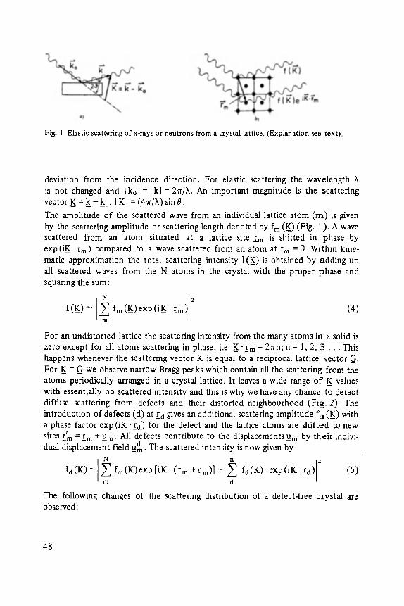
Fig. 1 Elas t ic sca t te r ing o f x- rays or n e u t r o n s f rom a c rys ta l lat t ice. (Exp l ana t i on see t ex t ) .
deviation from the incidence direction. For elastic scattering the wavelength X is not changed and Ikol = Ikl =2rr/X. An important magnitude is the scattering vector K = k - k o , I Ki -- (47r/~.) sin0.
The amplitude of the scattered wave from an individual lattice atom ( m ) is given by the scattering amplitude or scattering length denoted by fm (K_) (Fig. 1). A wave scattered from an atom situated at a lattice site r_m is shifted in phase by exp (iK_ "r_m) compared to a wave scattered from an atom at r_m --0. Within kine- matic approximation the total scattering intensity I(K_) is obtained by adding up all scattered waves from the N atoms in the crystal with the proper phase and squaring the sum:
N 2 I(_K) Z fm (_K)exp ( i K ' r m ) (4)
m
For an undistorted lattice the scattering intensity from the many atoms in a solid is zero except for all atoms scattering in phase, i.e. _K "rm = 2rrn; n = 1, 2, 3 ... . This happens whenever the scattering vector K_ is equal to a reciprocal lattice vector _G. For K = G we observe narrow Bragg peaks which contain all the scattering from the atoms periodically arranged in a crystal lattice. It leaves a wide range of" _K values with essentially no scattered intensity and this is why we have any chance to detect diffuse scattering from defects and their distorted neighbourhood (Fig. 2). The introduction of defects (d) at r a gives an additional scattering amplitude fa (K_) with a phase factor exp (iK_ "rd) for the defect and the lattice atoms are shifted to new sites r m = r m + Urn. All defects contribute to the displacements urn by their indivi- dual displacement field u d . The scattered intensity is now given by
ld(-K) ~ ~ n "r-a) 2 frn(_K)exp [ i K ' ~ r n +_Um)] + ~ fd(_K)" exp(i_K (5) r n d
The following changes of the scattering distribution of a defect-free crystal are observed:
48
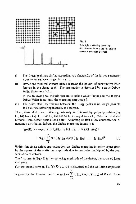
Fig. 2 Principle sca t ter ing in t ens i ty
d i s t r i bu t ion f rom a c rys ta l la t t ice
w i t h o u t and wi th defec t s
i) The Bragg peaks are shifted according to a change A a of the lattice parameter a due to an average changed lattice rm.
ii) Deviations from this average lattice decrease the amount of constructive inter- ference in the Bragg peaks. The attenuation is described by a static Debye- Waller factor exp ( -2L) .
In the following we include this static Debye-Waller factor and the thermal Debye-Waller factor into the scattering amplitude f.
iii) The destructive interference between the Bragg peaks is no longer possible and a diffuse scattering intensity is observed.
The diffuse distortion scattering intensity is obtained by properly subtracting Eq. (4) from (5). For this Eq. (5) has to be averaged over all possible defect distri- butions. Here defect correlations enter. Assuming at first a low concentration of randomly distributed defects, the diffuse scattering intensity is
Idiff(K ) = C exp ( - 2 L ) l fa (K_)exp (i_K "_rd) + if(K_)K_ - ~(~) +
N
+ f(K_) ~-~ exp (i_K "rm) (exp (i_K �9 urn) - 1 - iK_ " Um)l 2 (6) m
Within this single defect approximation the diffuse scattering intensity is just given by the square of the scattering amplitude due to one defect multiplied by the con- centration of defects.
The first term in Eq. (6) is the scattering amplitude of the defect, the so-called Laue scattering.
For the second term in Eq. (6) K_" u m < 1 is assumed and the scattering amplitude N
is given by the Fourier transform ~ (_K) = ~ _u r(rm ) exp (i_K" rrn) of the displace- m
49
ment field. Close to a Bragg peak G_ or small q = _K-_G, respectively, this term dominates and we observe Huang diffuse scattering which stems from the long range part of the displacement field. The third term in Eq. (6) is the scattering amplitude from the displacements of the near neighbours of the defect, for which _K" U_m > 1. From the total scattering amplitude of the lattice with distortions (first term in Eq. (5)) the Bragg intensity and the scattering intensity already considered in the second term of Eq. (6) are subtracted. Close to a Bragg peak the diffuse scattering is dominated by the Huang term, the coherent scattering from the long range displacement field. As we shall see later, the Huang diffuse scattering intensity is proportional to the square of the reciprocal distance q from the Bragg peak (l/q2). This magnification of the scattering from a defect is unique for Huang scattering and is e.g. absent in small angle scattering from defects.
Far away from a Bragg peak the second term is small enough that also the contri- butions from terms one and three can be observed. This is the reason why the diffuse scattering from regions between Bragg peaks ("Zwischenreflex" scattering) is considered to give information on the defect and its immediate neighbourhood.
So far we have assumed a random defect distribution and we obtained the total diffuse scattering intensity by adding the scattering intensities from the single defects. The interference term which would take into account scattered waves from different defects is averaged to zero for a random defect distribution. For correlated defect distributions this is no longer valid and the defect correlations have to be taken into account and Eq. (6) changes accordingly. Instead of the defect concentration the Fourier transform E(q_) of the concentration fluctuations cd (-[d) enters,
N'
~(q)= ~ (c a - c ' ) exp ( iq ' r c l ) . (7) d = l
Here ca is 0 or 1 if the defect site r a is empty or occupied, respectively. N' is the maximum number of possible defect sites and c' = C/Cma x the defect concentration related to the maximum concentration Cma x = N'/N of defects. The average over all equivalent defect distributions gives the factor that enters into Eq. (6) instead of the factor c:
(l~(_q)l 2) = c(1 - c ' ) + N' ~ e(p__)exp (iq" O_), (8) o~:0
with p_ = r a - r~ the distance between two defects and e (p__) a correlation function given by e(oo) = P(p_) - ,2 _ c , where PCo_) is the probability of finding another defect in the distance p_ from a given defect. In Eq. (8) the first term comes from a random
50
defect distribution and the second term from an additional correlation between the defects. For a small concentration (c' '~ 1) of randomly distributed defects <1 ~ (_q) 12 > = c and we have Eq. (6).
3 E x p e r i m e n t a l Resul ts for H y d r o g e n (Deu te r i um) in N i o b i u m
In the following we report on experimental results of investigations where hydrogen metal systems have been studied mainly by diffuse x-ray and neutron scattering. Niobium and niobium alloys are typical VB transition elements which dissolve large amounts of hydrogen.
3.1 Experimental Details
The experiments were performed on single crystals. After ultrahigh vacuum degas- sing they were loaded with hydrogen or deuterium from the gas phase. They were kept in the homogeneous ,v - r~' phase region either at low concentration for mea- surements at room temperature or by in situ loading at temperatures above the o~-a ' phase boundary. The hydrogen (deuterium) concentration was determined from weight increase, lattice parameter change or combined lattice parameter change, and Huang diffuse scattering measurements. For the x-ray scattering experi- ments sealed off x-ray tube generators as well as rotating anode generators (maxi- mum power 60 kW) were used. For the low intensity diffuse Zwischenreflex scattering a position sensitive detector in connection with a multichannel analyser and a microcomputer were used. The neutron scattering experiments were per- formed at the high flux reactor of the Institute Laue-Langevin in Grenoble. The three-axis spectrometers D 10 and IN 2 were used.
3.2 Lattice Parameter Change
The relative lattice parameter change Aa/a was measured from the shift of the Bragg peaks by Burkel [9] for niobium over a wide range of hydrogen and deuterium concentrations at 200 ~ Fig. 3 shows the results together with results from other authors. Up to a concentration of c < 0.3 H(D)/Nb AV/V increases linearly with the concentration c and is (AV/V)c = 0.174-+0.002 in agreement with the low concentration value [10]. With the well-known elastic constants Clt and C12,
= aa/2 and Eq. (3) one obtains Trace Pij = 10 eV and for the additional volume per defect Av = 0.17 ~2. For concentrations c > 0.3 H(D)/Nb there is a deviation from the linear increase as well as a small isotopic effect, hydrogen expands the nio- bium lattice a little more than deuterium. Such a deviation from a linear increase is expected if the elastic constants entering into Eq. (3) change with hydrogen concen- tration. Taking the elastic constants as measured as a function of hydrogen (deute- rium) concentration [9, 11] to evaluate Trace Pij leaves a small decrease of this magnitude with H(D) concentration. From this one has to conclude that also the Kanzaki forces in Eq. (2) decrease for higher concentrations. The change of the elastic constants and/or the Kanzaki forces seems to be different for hydrogen and deuterium.
51
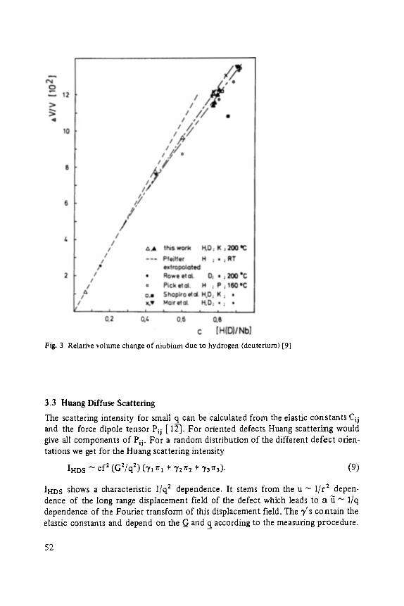
Fig. 3 Relative volume change of niobium due to hydrogen (deuterium) [9]
3.3 Huang Diffuse Scattering
The scattering intensity for small q can be calculated from the elastic constants Cij and the force dipole tensor Pij [ 12]. For oriented defects Huang scattering would give all components of Pii" For a random distribution of the different defect orien- tations we get for the Huang scattering intensity
IHD S ~ cf : (G2/q ~) (7,1rl + 721r2 + 731ra). (9)
IHD s shows a characteristic 1/q 2 dependence. It stems from the u ~ 1/r 2 depen- dence of the long range displacement field of the defect which leads to a ~ ~ 1/q dependence of the Fourier transform of this displacement field. The 7 's contain the elastic constants and depend on the G_ and q according to the measuring procedure.
52
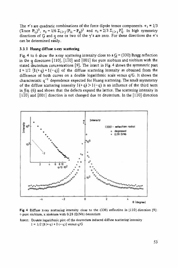
The zr's are quadratic combinations of the force dipole tensor components, rr I = I/3 (Trace Pij) 2, 7r 2 = 1/6 Yq>j (Pi i -Pj i )2 and lr3 =2 /3 Y.i>j P~j. In high symmetry directions of _G and q one or two of the 7 's are zero. For these directions the rr's can be determined easily.
3.3.1 Huang diffuse x-ray scattering
Fig. 4 to 6 show the x-ray scattering intensity close to a G = (330)Bragg reflection in the q directions [110], [11-0] and [001] for pure niobium and niobium with the stated deuterium concentrations [9]. The insert in Fig. 4 shows the symmetric part I = 1/2 [I(+ q)+ I ( - q ) l of the diffuse scattering intensity as obtained from the difference of both curves on a double logarithmic scale versus q/G. It shows the characteristic q-2 dependence expected for Huang scattering. The small asymmetry of the diffuse scattering intensity I ( + q ) > I ( - q ) is an influence of the third term in Eq. (6) and shows that the defects expand the lattice. The scattering_intensity in [11-0] and [001] direction is not changed due to deuterium. In the [110] direction
Fig. 4 Diffuse x-ray scattering intensity close to the (330) reflection in [110] direction [91: o pure niobium, x niobium with 0.28 (D/Nb) deuterium
Insert: Double logarithmic plot of the deuterium induced diffuse scattering intensity I - 1/2 [I (+ q) + I (-q)l versus q/G
53
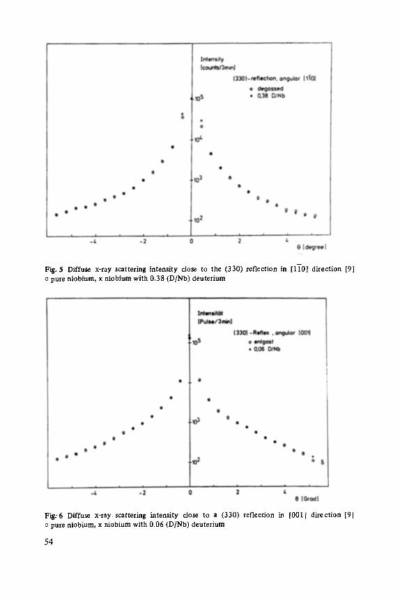
Fig. 5 Diffuse x-ray scattering intensity close to the (330) reflection in [1]-0] direction [9] o pure niobium, x niobium with 0.38 (D/Nb) deuterium
Fig:6 Diffuse x-ray scattering intensity close to a (330) reflection in [0011 direction [91 o pure niobium, x niobium with 0.06 (D/Nb) deuterium
54

close to (330) one has 3'~ = 3'3 = 0 and 3'2 ~ 0 and therefore rrz has to be zero. In the [001] direction close to (330) one has 3'1 = "Y2 = 0 and 3'3 ~ 0 and zr3 has to be zero. This means that the force dipole tensor for deuterium in niobium has cubic symmetry. If one converts the diffuse scattering intensity of Fig. 4 into absolute units one gets Pij = P ~ i j = 5ij (3.32 _+ 0.05)eV. Assuming a tetragonal t e n s o r Pi j = = (ABB) as expected from the site symmetry the agreement between the two curves in Fig. 5 within error bars leads to I A - B I < 0.2 eV. Fig. 6 sets an upper limit for the off diagonal tensor components which enter into 7r3, we get ~r3 < 0.2 eV 2. These experimental results for deuterium in niobium at 200 ~ are in very good agreement with the results for hydrogen in niobium at room temperature and small concentrations [13]. From Pij = (~ij 3.32 eV we obtain Trace Pij = 9.96 eV in excel- lent agreement with the value determined from lattice parameter changes at low concentrations (see 3.2).
From a combination of the lattice parameter change Aa/a ~ cP and Huang scatter- ing IHD S ~ cP 2 we are able to determine both c and P separately. The concentra- tions determined by this independent method agree quite well with the concen- trations determined from weight increase [13]. The most surprising result that the force dipole tensor and the displacement field have cubic symmetry deserves some discussion. The local tetragonal symmetry of the defect site (H(D) on tetrahedral sites [ 14]) is obviously not transmitted to the long range displacement field. This is in contrast to the solution of heavier interstitials like nitrogen in niobium where the symmetry of the interstitial site (octahedral) is transmitted to the long range displacement field [20]. It is always possible to find a force model that gives a force dipole tensor with cubic symmetry [ 13]. Assuming deuterium on tetrahedral inter- stitial sites and applying central forces to the next neighbours only Eq. (2) does not lead to a force dipole tensor with cubic symmetry. However, a force model with central forces on first and second neighbours with f ' = 1 eV/A and f2 = 0.23 eV/A gives a force dipole tensor in agreement with the experimental value.
3.3.2 Huartg diffuse scattering of neutrons
In the case of neutron scattering from niobium with deuterium the first term m Eq. (6) is not negligible. Compared to the distortion scattering from the niobium lattice deuterium has a scattering length of the right order of magnitude [15]. The third term in Eq. (6) is a small correction as discussed in chapter 3.1.1 and earlier [13]. For a random distribution of defect sites the scattering intensity close to a Bragg peak is
IHD S ~ c <l fd exp (iK "rtt) + if _K" ~(K_)12> (10)
The average is over all non-equivalent defect sites. The second term in Eq. (10) has been discussed in chapter 3.1.1 and we know it from x-ray scattering. Here the displacements at large distances from the defect enter and they have always the in- version symmetry u( rm) = - u ( - r m ) . Therefore the second term is a pure real
55
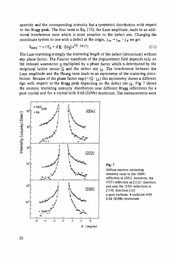
quantity and the corresponding intensity has a symmetric distribution with respect to the Bragg peak. The first term in Eq. (I0), the Lane amplitude, leads to an addi- tional interference term which is most sensitive to the defect site. Changing the coordinate system to one with a defect at the origin, r m -+I m - r d we get
~ iG'rd[~) IHD S ~ C ([fd + if_K" u(q)e - (11)
The Laue scattering is simply the scattering length of the defect (deuterium) without any phase factor. The Fourier transform of the displacement field depends onIy on the reduced wavevector q multiplied by a phase factor which is determined by the reciprocal lattice vector G and the defect site r d. The interference between the Laue amplitude and the Huang term leads to an asymmetry of the scattering distri- bution. Because of the phase factor exp (-i_G "rd) this asymmetry shows a different sign with respect to the Bragg peak depending on the defect site r d. Fig. 7 shows the neutron scattering intensity distribution near different Bragg reflections for a pure crystal and for a crystal with 0.68 (D/Nb) deuterium. The measurements were
Fig. 7 Diffuse neutron scattering intensity close to the (004) reflection in [001] direction, the (222) reflection in [111] direction and near the (330) reflection in [110] direction [15] x pure niobium. �9 niobium with 0.68 (D/Nb) deuterium
56

performed at 200 ~ in order to stay in the single phase region of the niobium- deuterium phase diagram. The intensity distributions were recorded near the (004) reflection in [001] direction, near the (222) reflection in [111] direction, and near the (330) reflection in [110] direction. The change of the asymmetry of the scatter- ing distribution is clearly visible. Near the (004) reflection the higher intensity lies at smaller angles, whereas for the (222) reflection increased intensity is observed at larger angles with respect to the Bragg reflections. The asymmetry in the vicinity of the (330) reflection is less pronounced but shows somewhat higher intensity on the large r angle side.
In order to interprete the observed asymmetric intensity distributions the phase factor e x p ( i G ' ~ ) in Eq. (11) has been calculated for different interstitial sites [9, 15]. The 12 tretrahedral sites or the 6 octahedral sites within the bcc lattice of niobium were assumed as possible sites for deuterium. Only the tetrahedral sites give a change of the asymmetry in accordance with the experimental observations. E.g. for an octahedral site occupation an asymmetry on the same side of the Bragg reflections would be expected near the (004) and the (222) reflections. These results have confirmed that deuterium mainly occupies tetrahedral sites in niobium [14].
3.4 Zwischenreflex Scattering
For the scattering at large q between the Bragg reflections the measured intensity distributions have to be compared to calculated ones for different defect models. The displacements Urn (r) and their Fourier transform ~(K_) are calculated by lattice statics as described in chapter 2.1. In general all three terms in Eq. (6) give contri- butions of about the same order of magnitude.
3.4.1 Zwischenreflex scattering of x-rays
For x-ray scattering term one in Eq. (6) is negligible whereas the other two terms are of the same magnitude but rather small compared to the scattering close to the Bragg peaks, where the background to be subtracted is mainly thermal diffuse scat- tering and little Compton scattering and parasitic (air, slits, windows etc.) scattering. It has about the same magnitude as the Huang scattering intensity and can be taken into account by subtracting the scattering intensity from the crystal before defects were introduced. In the region between Bragg reflections the background scattering is dominated by Compton scattering and some thermal diffuse scattering.
The Zwischenreflex scattering due to distorting defects gives intensities typically 1% to 10 % of the background scattering. Therefore, one has to use high power x-ray generators, e.g. rotating anode generators or synchrotron radiation sources and position sensitive detectors in order to detect the wanted intensity at such a low signal to noise level with reasonable statistics. Fig. 8 shows a typical plot of the raw data in order to demonstrate the x-ray scattering intensity difference between
57
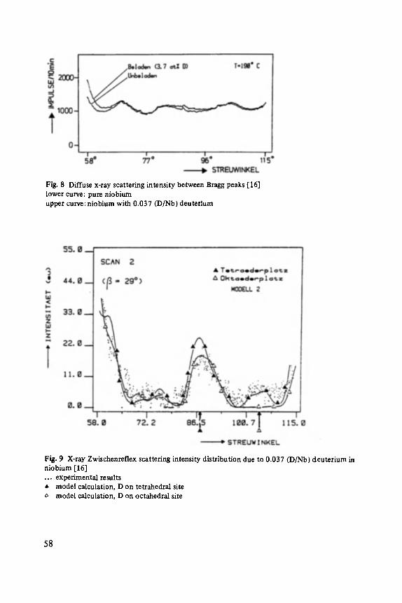
Fig. 8 Diffuse x-ray scattering intensity between Bragg peaks [ 16] lower curve: pure niobium upper curve: niobium with 0.037 (D/Nb) deuterium
Fig. 9 X-ray Zwischenreflex scattering intensity distribution due to 0.037 (D/Nb) deuterium in niobium [16] ... experimental results �9 model calculation, D on tetrahedral site
model calculation, D on octahedral site
58
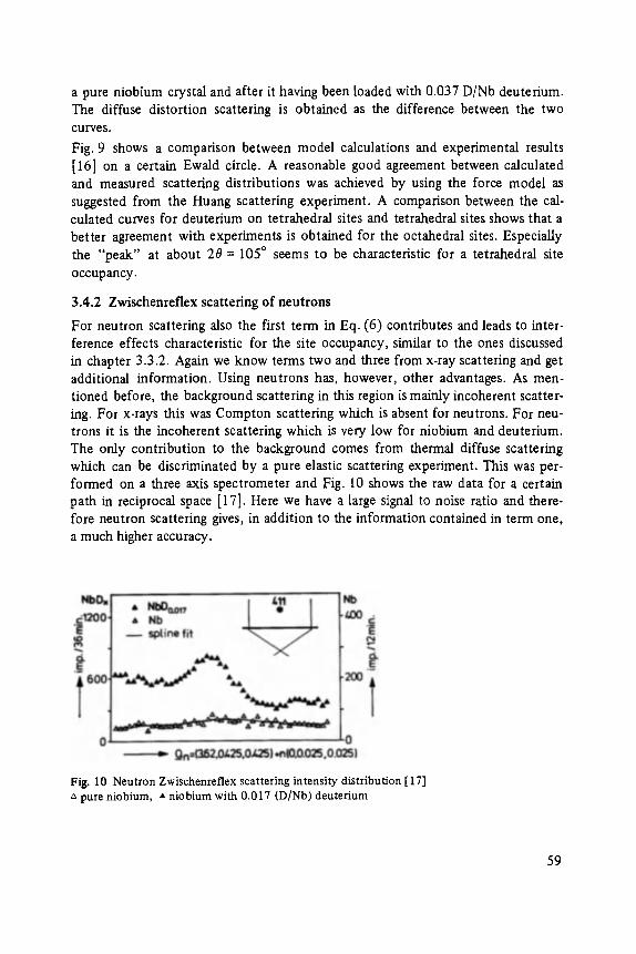
a pure niobium crystal and after it having been loaded with 0.037 D/Nb deuterium. The diffuse distortion scattering is obtained as the difference between the two curves .
Fig. 9 shows a comparison between model calculations and experimental results [16] on a certain Ewald circle. A reasonable good agreement between calculated and measured scattering distributions was achieved by using the force model as suggested from the Huang scattering experiment. A comparison between the cal- culated curves for deuterium on tetrahedral sites and tetrahedral sites shows that a better agreement with experiments is obtained for the octahedral sites. Especially the "peak" at about 20 = 105 ~ seems to be characteristic for a tetrahedral site occupancy.
3.4.2 Zwischenreflex scattering of neutrons
For neutron scattering also the first term in Eq. (6) contributes and leads to inter- ference effects characteristic for the site occupancy, similar to the ones discussed in chapter 3.3.2. Again we know terms two and three from x-ray scattering and get additional information. Using neutrons has, however, other advantages. As men- tioned before, the background scattering in this region is mainly incoherent scatter- ing. For x-rays this was Compton scattering which is absent for neutrons. For neu- trons it is the incoherent scattering which is very low for niobium and deuterium. The only contribution to the background comes from thermal diffuse scattering which can be discriminated by a pure elastic scattering experiment. This was per- formed on a three axis spectrometer and Fig. 10 shows the raw data for a certain path in reciprocal space [17]. Here we have a large signal to noise ratio and there- fore neutron scattering gives, in addition to the information contained in term one, a much higher accuracy.
Fig. 10 Neutron Zwischenreflex scattering intensity distribution [ 17] zx pure niobium, �9 niobium with 0.017 (D/Nb) deuterium
59
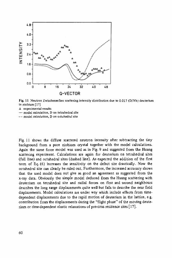
Fig. 11 Neutron Zwischenreflex scattering intensity distribution due to 0.017 (D/Nb) deuterium in niobium [17]
experimental results - - model calculation, D on tetrahedral site --- model calculation, D on octahedral site
Fig. 11 shows the diffuse scattered neutron intensity after subtracting the tiny background from a pure niobium crystal together with the model calculations. Again the same force model was used as in Fig. 9 and suggested from the Huang scattering experiment. Calculations are again for deuterium on tetrahedral sites (full line) and octahedral sites (dashed line). As expected the addition o f the first term of Eq. (6) increases the sensitivity on the defect site drastically. Now the octahedral site can clearly be ruled out. Furthermore, the increased accuracy shows that the used model does not give as good an agreement as suggested from the x-ray data. Obviously the simple model deduced from the Huang scattering with deuterium on tetrahedral site and radial forces on first and second neighbours describes the long range displacements quite well but fails to describe the near field displacements. Model calculations are under way which include effects f rom time- dependent displacements due to the rapid motion of deuterium in the lattice, e.g. contribution from the displacements during the "flight phase" of the moving deute- rium or time-dependent elastic relaxations of previous residence sites [17].
60
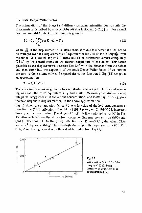
3.5 Static Debye-Waller Factor
The attenuation of the Bragg (and diffuse) scattering intensities due to static dis- placements is described by a static Debye-Waller factor exp ( -2 L) [18]. For a small random interstitial defect distribution it is given by
2 L = 2 c ( ~ ( c o s K �9 d _ _u m - l ) } (12) i n
where Uam is the displacement of a lattice atom at m due to a defect at d. 2 L has to be averaged over the displacements of equivalent interstitial sites d. Using Udm from the model calculations e x p ( - 2 L ) turns out to be determined almost completely (95 %) by the contributions of the nearest neighbours of the defect. This seems plausible as the displacements decrease like 1/r 2 with the distance from the defect and then enter into the exponent of the static Debye-Waller factor. If we restrict the sum to these atoms only and expand the cosine function in Eq. (12) we get as an approximation
2L = 4/3 cK2u~ (13)
There are four nearest neighbours to a tetrahedral site in the bcc lattice and averag- ing was over the three equivalent x, y and z sites. Measuring the attenuation of integrated Bragg intensities for various concentrations and scattering vectors _K gives the next neighbour displacement ul in the above approximation.
Fig. 12 shows the attenuation factor 2L as a function of the hydrogen concentra- tion for the (220) reflection of niobium [19]. Up to c = 0.2 (H/Nb) 2L increases linearly with concentration. The slope 2L/c of this line is plotted versus K 2 in Fig. 13. Also included are the slopes from corresponding measurements on (h00) and (hhh) reflections. Up to the (330) reflection, i.e. K2~ 65 A -2, the values 2L/c versus K 2 lay on a straight line through the origin. Its slope gives ul = (0.100-+ 0.07) A in close agreement with the calculated value from Eq. (1).
Fig. 12 Attenuation factor 2L of the integrated (220) Bragg intensity as a function of H concentration [19]
61
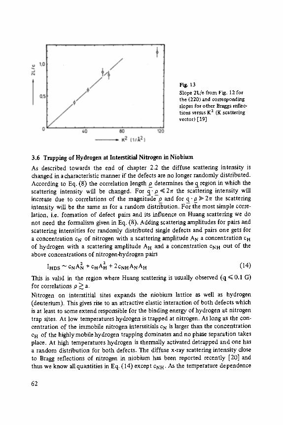
Fig. 13 Slope 2L/e from Fig. 12 for the (220) and corresponding slopes for other Braggs reflec- tions versus K 2 (K scattering vector) [ 19]
3.6 Trapping of Hydrogen at Interstitial Nitrogen in Niobium
As described towards the end of chapter 2.2 the diffuse scattering intensity is changed in a characteristic manner if the defects are no longer randomly distributed. According to Eq. (8) the correlation length p_ determines the q region in which the scattering intensity will be changed. For q ' p ,~ 27r the scattering intensity will increase due to correlations of the magnitude p and for q" p >> 2~r the scattering intensity will be the same as for a random distribution. For the most simple corre- lation, i.e. formation of defect pairs and its influence on Huang scattering we do not need the formalism given in Eq. (8). Adding scattering amplitudes for pairs and scattering intensities for randomly distributed single defects and pairs one gets for a concentration CN of nitrogen with a scattering amplitude AN a concentration CH of hydrogen with a scattering amplitude A H and a concentration cN8 out of the above concentrations of nitrogen~hydrogen pairs
2 IHDS ~ CNA~ q + CHA H + 2CNHANAH (14)
This is valid in the region where Huang scattering is usually observed (q < 0.1 G) for correlations p ~> a.
Nitrogen on interstitial sites expands the niobium lattice as well as hydrogen (deuterium). This gives rise to an attractive elastic interaction of both defects which is at least to some extend responsible for the binding energy of hydrogen at nitrogen trap sites. At low temperatures hydrogen is trapped at nitrogen. As long as the con- centration of the immobile nitrogen interstitials CN is larger than the concentration CH of the highly mobile hydrogen trapping dominates and no phase separation takes place. At high temperatures hydrogen is thermally activated detrapped and one has a random distribution for both defects. The diffuse x-ray scattering intensity close to Bragg reflections of nitrogen in niobium has been reported recently [20] and thus we know all quantities in Eq. (14) except CNH. As the temperature dependence
62
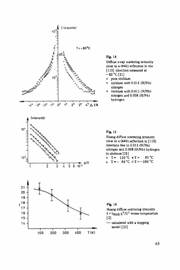
Fig. 14 Diffuse x-ray scattering intensity close to a (4407 reflection in the [110] direction measured at - 80 ~ [ 2 1 ]
o pure niobium + niobium with 0.011 (N/Nb)
nitrogen zx niobium with 0.011 (N/Nb)
nitrogen and 0.008 (H/Nb) hydrogen
Fig. 15 Huang diffuse scattering intensity close to a (4407 reflection in [110] direction due to 0.011 (N/Nb) nitrogen and 0.008 (H/Nb) hydrogen in niobium [21] + T= 150"C "T = 50"C x T = - 80~ o T = - 1 8 0 ~
F~. 16
Huang diffuse scattering intensity I = IHD S q2/G2 versus temperature [2] - - calculated with a trapping
model [23]
63
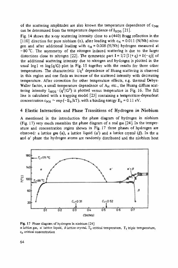
of the scattering amplitudes are also known the temperature dependence of CNH can be determined from the temperature dependence of IHD s [21].
Fig. 14 shows the x-ray scattering intensity close to a (440) Bragg reflection in the [1 I0] direction for pure niobium (o), after loading with c,~ = 0.011 (N/Nb) nitro- gen and after additional loading with c H = 0.008 (H/Nb) hydrogen measured at - 8 0 ~ The asymmetry of the nitrogen induced scattering is due to the larger distortions close to nitrogen [22]. The symmetric part I = 1/2 [ I (+q )+ I ( - q ) ] of the additional scattering intensity due to nitrogen and hydrogen is plotted in the usual logI vs log(q/G) plot in Fig. 15 together with the remits for three other temperatures. The characteristic 1/q 2 dependence of Huang scattering is observed in this region and one finds an increase of the scattered intensity with decreasing temperature. After correction for other temperature effects, e.g. thermal Debye- Waller factor, a small temperature dependence of AN etc., the Huang diffuse scat- tering intensity IHDS" (q2/GZ) is plotted versus temperature in Fig. 16. The full line is calculated with a trapping model [23] containing a temperature-dependent concentration CNH ~ exp (-Eb/kT), with a binding energy Eb = 0.11 eV.
4 Elast ic I n t e r a c t i o n and Phase Trans i t ions o f H y d r o g e n in N i o b i u m
A mentioned in the introduction the phase diagram of hydrogen in niobium (Fig. 17) very much resembles the phase diagram of a real gas [24]. In the temper- ature and concentration region shown in Fig. 17 three phases of hydrogen are observed: a lattice gas (ct), a lattice liquid (tv') and a lattice crystal (/~). In the c~ and a ' phase the hydrogen atoms are randomly distributed and the niobium host
Fig. 17 Phase diagram of hydrogen in niobium [24] a lattice gas, ,~' lattice liquid, fl lattice crystal, T c critical temperature, T t triple temperature, c c critical concentration
64
lattice retains its cubic symmetry. The only difference between a and a ' is the higher concentration of the a ' phase. The hydrogen is highly mobile in the metal lattice. Mobility at room temperature is of the same order of magnitude as in a fluid like water. As the second alloy component is immobile, hydrogen in metals behaves like a one-component fluid penetrating the metal lattice. Hydrogen in metals is one of the few solid systems where thermal equilibrium is quickly attained. It is obvious to consider hydrogen in niobium as a text book example for the lattice gas model of fluids [25]. It has been suggested by Alefeld [25] that the relevant attractive interaction causing the gas-liquid ( a - a ' ) transition is an elastic interaction trans- mitted through the elastic distortions of the metal lattice due to hydrogen. It is energetically more favourable for hydrogen to stay in a lattice already expanded by others. This long range elastic interaction can be formulated in terms of the force dipole tensor Pij and the elastic compliances Sijkl of the metal lattice. For a random distribution of hydrogen it is
1 ~ ( 1 5 ) ~ Wab = c2pij SijklPkl ab
Together with a short range repulsive interaction which is not well known the cal- culated phase diagrams [27, 28] are in reasonable good agreement with the experi- mental one shown in Fig. 17.
In one respect the phase transition a - a ' of hydrogen in niobium shows a feature completely different from the behaviour of a real fluid. This also originates from the elastic interaction. If a niobium crystal with hydrogen (e.g. with the critical concentration ce = 0.31 H/Nb) is cooled below the critical temperature into the two phase region a - a ' the system will separate into the low concentration c~ phase and the high concentration a ' phase. Due to the different concentrations the lattice will be differently expanded in the a and a ' phase and elastic stresses are created at the phase boundaries. As long as the metal lattice stays coherent these coherency stresses alter the free energy of the system, the elastic energy is thereby reduced and the phase transition suppressed. Large fluctuations which normally occur close to a critical point are also strongly suppressed because they would cause large coherency stresses. Only certain hydrogen concentration fluctuation modes exist. This leads to the concept of elastic modes as introduced by Wagner and Horner [4]. The details of the elasticity theory and thermodynamics involved in these calculations are rather complicated and it is referred to the special literature [5, 4]. A brief summary of the essential results will be given here. It turns out that the calculation of the elastic energy for an arbitrary density fluctuation c ~ ) , by solving the proper boundary value problems, leads to an eigenvalue problem, in which the fluctuations can be analysed in terms of eigenmodes ffL (J-) of the elastic energy:
c(r) = E CL f f t .~) (16) L
65
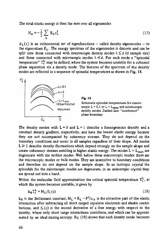
The total elastic energy is then the sum over all eigenmodes
1 Hel=-~ ~ ELC [ (17) L
~L(f - ) is an orthonormal set of eigenfunctions - called density eigenmodes - to the eigenvalues EL. The energy spectrum of the eigenmodes is discrete and can be split into those connected with macroscopic density modes ~ ~< d (d sample size) and those connected with microscopic modes ;k,~ d. For each mode a "'spinodal temperature" T L may be defined, where the system becomes unstable for a coherent phase separation via a density mode. The features of the spectrum of the density modes are reflected in a sequence of spinodal temperatures as shown in Fig. 18.
F~. ~8 Schematic spinodal temperatures for macro- scopic L = 0,1 to L = Lmax and microscopic density modes. Dashed Line: " incoherent" phase boundary
The density modes with L = 0 and L = 1 describe a homogeneous density and a constant density gradient, respectively, and have the lowest elastic energy because they are not accompanied by coherency stresses. They do not depend on the boundary conditions and occur in all samples regardless of their shape. All modes L i> 2 describe density fluctuations which depend strongly on the sample shape and create coherency stresses resulting in higher elastic energy. The modes L = Lma x are degenerate with the surface modes. Well below these macroscopic modes there are the microscopic modes or bulk modes. They are insensitive to boundary conditions and therefore do not depend on the sample shape. In an isotropic crystal the spin0dals for the microscopic modes are degenerate, in an anisotropic crystal they are spread out into a band.
Within the molecular field approximation the critical spinodal temperature TLs, at which the system becomes unstable, is given by
kaT E = Ms/f2 (c) (18)
ka is the Boltzmann constant, M L = Er. - P2/cn is the attractive part of the elastic interaction after subtracting all short ranged repulsive electronic and elastic contri- butions, and f2 (c) is the second derivative of a free energy with respect to the density, where only short range interactions contribute, and which can be approxi- mated by an ideal mixing entropy. Eq. (18) shows that each density mode becomes
66
unstable at a different temperature. The spinodal temperatures Ts ~ for the homo- geneous and the constant gradient mode have the highest critical temperature which is identical with T e for an "incoherent" phase transition. Between this "incoherent" T c and the spinodal temperature of the microscopic modes there exists a series of spinodals, each connected with a macroscopic mode. Consequently, the number of modes contributing to critical fluctuations in the vicinity of T e is strongly sup- pressed when compared to a normal fluid where the spectrum of critical fluctua- tions is continuous.
The so-called "incoherent" phase boundary (coexistence curve) and the "incoherent" spinodal are the only ones where coherency stresses do not play a part. They are also the only ones where the analogy to real fluid holds. In order to observe the incoherent phase separation of hydrogen in niobium it is necessary that dislocations reduce the coherency stresses to zero. As the creation of dislocations needs a certain minimum stress, complete incoherency is an ideal state [24]. In the same sense a pure coherent state is an ideal state where no coherency stresses are released by the creation of dislocations. Delicate experimental conditions can approach these ideal states [24, 29, 30].
5 Expe r imen ta l Observat ion o f Phase Transi t ions and Densi ty Modes o f H y d r o g e n in Niob ium
5.1 Local Lattice Parameter Measurements
As discussed in chapter 3.2 the measured x-ray lattice parameter change can be used to determine the hydrogen concentration. In such an experiment [24] the hydrogen concentration is kept constant and the lattice parameter of niobium is measured as a function of temperature. The principle of the method is demonstrated in Fig. 19. A niobium crystal is charged with hydrogen from the gas phase above Te- The Bragg peak changes its position due to the lattice expansion caused by a certain hydrogen concentration (e.g. the critical concentration as shown in Fig. 19). In the homo- geneous single-phase region above Tc the shape of the Bragg peak is not changed. Below Tc hydrogen inhomogeneities cause a broadening and asymmetry of the Bragg peak. If an incoherent phase separation tx - ix' occurs the Bragg peak splits into two sharp and symmetric Bragg peaks according to the two phases cz and ct' with homo- geneous concentrations c~, and ca', respectively.
The incoherent phase diagram shown in Fig. 17 was determined in this manner.
5.2 Macroscopic Hydrogen Density Modes
Coherent density fluctuations below Tc are connected with macroscopic variations of the hydrogen concentration in the sample. Hydrogen density fluctuations leading to a macroscopic density mode have been observed above T e from measuring the line width of an x-ray Bragg peak. MoK~ radiation was used in order to have a large
67

Fig. 19 Principle of the experimental method: Phase diagram, hydrogen density d i s t r ibu t ion Bragg reflections for a homogeneous phase at T > Tc, a coherent phase separation wi th a macro- scopic densi ty mode at T - T c r T e, and an incoherent phase separation with a d i scont inuous densi ty at T < T c
Fig. 20 Broadening o f an x-ray reflection d u e to a macroscopic hydrogen density mode in niobium. The inverse o f the square o f the addit ional line width is plotted versus temperature [31 ]
68
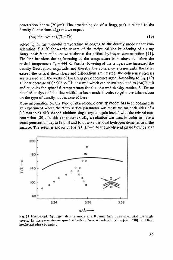
penetration depth (70 gin). The broadening Aa of a Bragg peak is related to the density fluctuations c(5_) and we expect
(Aa) -~ ~ ~c 2 ~ 1/(T - T L) (19)
where T L is the spinodal temperature belonging to the density mode under con- sideration. Fig. 20 shows the square of the reciprocal line broadening of a x-ray Bragg peak from niobium with almost the critical hydrogen concentration [31]. The line broadens during lowering of the temperature from above to below the critical temperature Tc = 44"!. K. Further lowering of the temperature increased the density fluctuation amplitude and thereby the coherency stresses until the latter exceed the critical shear stress and dislocations are created, the coherency stresses are released and the width of the Bragg peak decreases again. According to Eq. (19) a linear decrease of (Aa) -~ vs T is observed which can be extrapolated to (Aa) -2 = 0 and supplies the spinodal temperatures for the observed density modes. So far no detailed analysis of the line width has been made in order to get more information on the type of density modes excited here.
More information on the type of macroscopic density modes has been obtained in an experiment where the x-ray lattice parameter was measured on both sides of a 0.3 mm thick disk-shaped niobium single crystal again loaded with the critical con- centration [30]. In this experiment CuKa x-radiation was used in order to have a small penetration depth (8/~m) and to observe the local hydrogen densities near the surface. The result is shown in Fig. 21. Down to the incoherent phase boundary at
Fig. 21 Macroscopic hydrogen density mode in a 0.3 mm thick disk-shaped niobium single crystal. Lattice parameter measured at both surfaces as sketched by the insert [30]. Full line: incoherent phase boundary
69
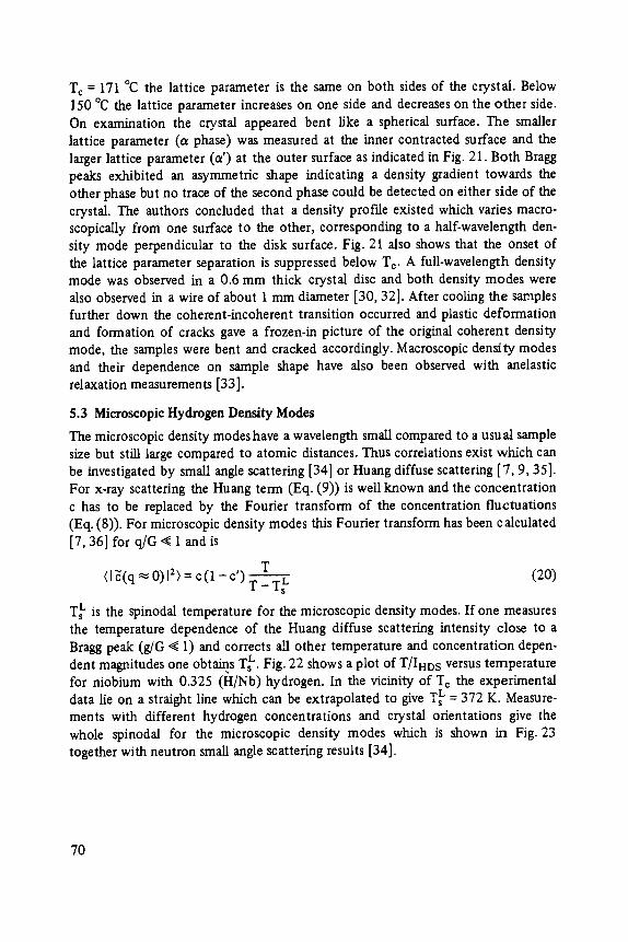
T e = 171 ~ the lattice parameter is the same on both sides of the crystal. Below 150 ~ the lattice parameter increases on one side and decreases on the other side. On examination the crystal appeared bent like a spherical surface. The smaller lattice parameter (o phase) was measured at the inner contracted surface and the larger lattice parameter (o') at the outer surface as indicated in Fig. 21. Both Bragg peaks exhibited an asymmetric shape indicating a density gradient towards the other phase but no trace of the second phase could be detected on either side of the crystal. The authors concluded that a density profile existed which varies macro- scopicaUy from one surface to the other, corresponding to a half-wavelength den- sity mode perpendicular to the disk surface. Fig. 21 also shows that the onset of the lattice parameter separation is suppressed below T e. A full-wavelength density mode was observed in a 0.6 mm thick crystal disc and both density modes were also observed in a wire of about 1 mm diameter [30, 32]. After cooling the samples further down the coherent-incoherent transition occurred and plastic deformation and formation of cracks gave a frozen-in picture of the original coherent density mode, the samples were bent and cracked accordingly. Macroscopic density modes and their dependence on sample shape have also been observed with anelastic relaxation measurements [33].
5.3 Microscopic Hydrogen Density Modes
The microscopic density modes have a wavelength small compared to a usual sample size but still large compared to atomic distances. Thus correlations exist which can be investigated by small angle scattering [34] or Huang diffuse scattering [7, 9, 35]. For x-ray scattering the Huang term (Eq. (9)) is well known and the concentration c has to be replaced by the Fourier transform of the concentration fluctuations (Eq. (8)). For microscopic density modes this Fourier transform has been calculated [7, 36] for q/G ,~ 1 and is
T (20) (l~(q ~ 0)12) = c(1 - c ' ) T - r---~
T L is the spinodal temperature for the microscopic density modes. If one measures the temperature dependence of the Huang diffuse scattering intensity close to a Bragg peak (g/G "~ 1) and corrects all other temperature and concentration depen- dent magnitudes one obtains Ts L. Fig. 22 shows a plot of T/IHD s versus temperature for niobium with 0.325 (FI/Nb) hydrogen. In the vicinity of Tr the experimental data lie on a straight line which can be extrapolated to give T L = 372 K. Measure- ments with different hydrogen concentrations and crystal orientations give the whole spinodal for the microscopic density modes which is shown in Fig. 23 together with neutron small angle scattering results [34].
70

Fig. 22
Temperature dependence of the Huang diffuse scattering intensity due to 0.32 (D/Nb) deuterium in niobium [9, 35]
Fig. 23
Phase diagram of deuterium in niobium with incoherent spinodal ( . . . . . ) [34] and spinodals for microscopic density modes: - - - neutron small angle scattering [34] . . . . Huang diffuse scattering [9,3 5]
Acknowledgements This report was possible because I had exceUent students and co-workers who participated in this research project during the last years: H. Behr, E. Burkel, H. Metzger, H. Pfeiffer, U. Schubert, and H. ZabeL I cordially thank them for the fruitful and pleasant coUaboration. My special thanks go to H. Dosch and W. Fenzl for their contributions and stimulating discussions during the preparation of this report.
The research work was supported by the Bundesministerium fiir Forschung und Technologie.
71
References
[1]
[2]
[3]
[43
[5]
[6]
[7]
[8]
[9]
[lO]
[11]
[12]
[13]
[14]
[15]
[16]
[17]
[18]
[19]
[20]
[21]
[22]
[23]
[24]
[25]
[26]
[27]
[28]
[29]
[30]
[31]
[323 [33]
[34]
[35]
[36]
H.
H.
E.
H.
H.
H.
H.
U.
U.
U.
G.
H.
For a review see: Hydrogen in Metals, Topics in Applied Physics, Vol. 28 and 29, Ed.: G. Alefeld, J. V61kl, Springer Verlag Berlin, Heidelberg, New York 1978.
H. Peisl in [I], I, p. 53.
G. Alefeld, phys. star. sol. 32, 67 (1969). H. Wagner and H. Horner, Advances in Physics 23, 587 (1974).
H. Wagner in [1], I, p. 5.
Ch. A. Wert in [1], II, p. 305.
W. Fenzl, Doctoral Thesis, University of Munich 1983.
For a review see e.g.: 1-1. Peisl, J. de Physique 37, C7-47 (1976). P. Ehrhart, J. of Nucl. Mat. 69 & 70, 200 (1978).
E. Burkel, Doctoral Thesis, University of Munich 1982.
H. Pfeiffer and H. Peisl, Physics Letters 60A, 363 (1977). F. M. Mazzolai and H. K. Birnbaum, Proc. 7th Int. Conf. of Int. Friction and Ultrasonic Attenuation in Solids, Lausanne 1981.
H. Trinkaus, phys. stat. sol. (b) 51,307 (1972).
Metzger, J. Peisl, andJ. Wanagel, J. Phys. F: Metal Phys. 6, 2195 (1976).
D. Carstanfen and R. Sizrnann, Physics Letters 40A, 93 (1972).
Burkel, H. Dosch, and,/. Peisl, Z. Phys. B, Condensed Matter 53, 33 (1983).
Dosch, Diploma Thesis, University of Munich 1980.
Dosch, unpublished results.
Metzger, H. Behr, and J. Peisl, Z. Phys. B, Condensed Matter 46,295 (1982).
Metzger, H. Behr, and,/. Peisl, Sol. State Comm. 40, 789 (1981).
Schubert, H. Metzger, and J. Peisl, J. Phys. F: Metal Phys. in press.
Schubert, 1-1. Metzger, and 3". Peisl, to be published.
Schubert, 1t. Dosch, H. Metzger, and 3". Peisl, J. Phys. F: Metal Phys., in press.
Pfeiffer and H. Wipf, J. Phys. F: Metal Phys. 6, 167 (1976).
Zabel and 3". Peisl, J. Phys. F: Metal Phys. 9, 1461 (1979).
R. Fowler and E. A. Guggenheim, Statistical Thermodynamics, Cambridge University Press, Cambridge 1960.
G. Alefeld, phys. stat. sol. 32, 67 (1969).
H. Horner and H. Wagner, J. Phys. C: Solid State Phys. 7, 3305 (1974).
M. Futran, S. G. Coasts, C. K. Hall, and D. O. Welch, J. Chem. Phys. 77, 6223 (1982).
H. Zabel, Doctoral Thesis, University of Munich 1978.
H. Zabel and J. Peisl, Acta Met. 28, 589 (1980).
H. Behr, unpublished results.
H. Zabel and J. Peisl, Phys. Rev. Lett. 42, 511 (1979).
J. Tretkowskh J. V61kl, and G. Alefeld, Z. Phys. B: Condensed Matter 28, 259 (1977).
W. Miinzing, Doctoral Thesis, Technical University of Munich (1978).
E. Burkel, W. Fenzl, and J. Peisl, to be published.
S. Dietrich and W. Fenzl, to be published.
72
Festk6rperprobleme XXIV (1984)
Inelastic Electron Tunneling Spectroscopy
Siegfried Ewert 2. Physikalisches Institut der Rheinisch-Westfw Teehnischen Hochschule Aachen, Aachen, Federal Republic of Germany
Summary: Inelastic Electron Tunneling Spectroscopy (IETS) is a method to measure vibronic and electronic excitation of molecules deposited as interlayers in tunnel junctions. In this article the method itself is briefly discussed and compared with other techniques of surface vibrational spectroscopy. As examples, investigations by IETS on sublimated phthalocyanine dye molecules, on ultrahigh vacuum prepared AI/A1 oxide/Pb tunnel junctions and on proton- irradiated AI/AI oxide + HCOO-/Pb tunnel junctions are reviewed. Tunneling measurements performed on n-Si/SiO2/metal structures with very thin SiO2 layers are reported and the results are discussed.
Introduction
Inelastic Electron Tunneling Spectroscopy (IETS) is a method for measuring the vibrational spectrum of molecules deposited as interlayers in tunnel junctions. The lETS was discovered by R.C.Jaklevic and J.Lambe [1]. In the following the prin- ciple of the method is briefly described (Fig. 1). The left part of Fig. 1 shows qualitatively and schematically the band model for a metal/insulator]metal tunnel junction with an applied external bias U. Because of the quantum mechanical tunneling effect electrons can tunnel elastically from filled states of metal I through the insulating barrier into empty electronic states in metal II. The tunneling current i is proportional to the tunneling probability, which depends on the geometry of the barrier, as well as on the number of filled states in metal I and the number of empty states in metal II.
IETS experiments are commonly carried out at low temperatures (4.2 K). At these temperatures the Fermi distribution function near EF is scarcely smeared out. If the applied potential becomes larger than kT then tunneling processes take place only from the negatively biased electrode to the positively biased electrode. Most electrons tunnel elastically through the barrier. The tunneling probability is so small that the occupation of the states in the metal electrodes is not affected by the tunneling current. In the barrier region there exist a lot of excitations of solids, like lattice vibrations of the insulator, of the electrodes, and vibronic or electronic excitations of adsorbed molecular species on the tunneling barrier. The tunneling electrons can interact with these excitations. As the applied potential e U is in- creased above the excitation energy, a new inelastic channel for tunneling is opened
73

Fig. 1 Schematic band diagram for a metal/insulator/meta/ tunnel junction with an applied external voltage U, elastic and inelastic tunneling are marked by arrows, rata o is a characteristic transition energy of an excitation within the insulating barrier. The inelastic tunneling produces an increase in the slope of the current I, a step in the conductivity dI/dU and a peak in the second derivative d2I/dU 2 versus voltage at Uo = hwo/e.
(Fig. 1). At the potential e U = laCOo the tunneling probability is enhanced and an additional contribution occurs in the tunneling current. In the right part of Fig. 1 this increase is shown exaggerated. The step in the conductivity is at about 1% and appears as a peak-like structure in the second derivative d 2 l/dU 2 of the tunneling characteristic. Each peak represents the energy position of a vibrational mode of energy hw0. In comparison with optical excitations, in IETS both infrared and Raman-active vibrational modes of molecules can be observed. While tunneling the electric field of the electron interacts with a dynamic dipole moment or with an induced dipole moment of the molecule. The electrons hereby lose the necessary energy for exciting the molecule to a higher energetic vibrational state [ 2 - 5 ] . Using Coulomb potentials for the inelastic interaction between the tunneling elec- trons and the molecular oscillators within the tunneling barrier the validity o f an "orientational selection rule" was theoretically derived: The tunneling electrons preferentially excite those vibrational modes, which have a component of their dynamic dipole moment perpendicular to the interface. Accordingly oscillators oriented parallel to the direction of the tunneling electrons give rise to much stronger IETS peaks than vibrations parallel to the interface [4, 5].
74
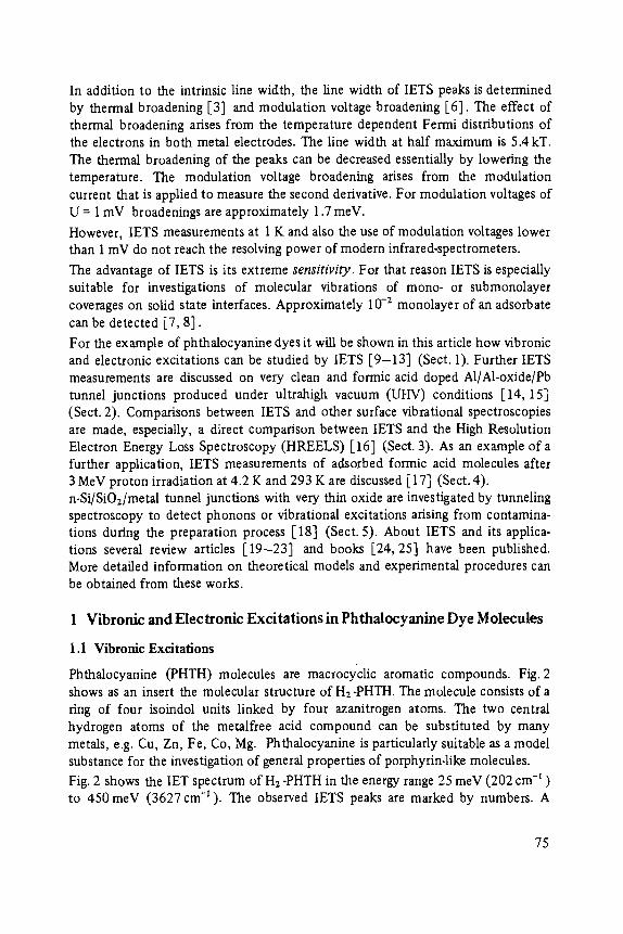
In addition to the intrinsic line width, the line width of IETS peaks is determined by thermal broadening [3] and modulation voltage broadening [6]. The effect of thermal broadening arises from the temperature dependent Fermi distributions of the electrons in both metal electrodes. The line width at half maximum is 5.4 kT. The thermal broadening of the peaks can be decreased essentially by lowering the temperature. The modulation voltage broadening arises from the modulation current that is applied to measure the second derivative. For modulation voltages of U = 1 mV broadenings are approximately 1.7 meV.
However, lETS measurements at 1 K and also the use of modulation voltages lower than 1 mV do not reach the resolving power of modern infrared-spectrometers.
The advantage of lETS is its extreme sensitivity. For that reason IETS is especially suitable for investigations of molecular vibrations of mono- or submonolayer coverages on solid state interfaces. Approximately 10 -2 monolayer of an adsorbate can be detected [7, 8].
For the example of phthalocyanine dyes it will be shown in this article how vibronic and electronic excitations can be studied by lETS [9-13] (Sect. 1). Further IETS measurements are discussed on very clean and formic acid doped A1/Al-oxide/Pb tunnel junctions produced under ultrahigh vacuum (UHV) conditions [14, 15] (Sect. 2). Comparisons between IETS and other surface vibrational spectroscopies are made, especially, a direct comparison between lETS and the High Resolution Electron Energy Loss Spectroscopy (HREELS) [16] (Sect. 3). As an example of a further application, IETS measurements of adsorbed formic acid molecules after 3 MeV proton irradiation at 4.2 K and 293 K are discussed [ 17] (Sect. 4). n-Si/SiO2/metal tunnel junctions with very thin oxide are investigated by tunneling spectroscopy to detect phonons or vibrational excitations arising from contamina- tions during the preparation process [ 18] (Sect. 5). About IETS and its applica- tions several review articles [19-23] and books [24, 25] have been published. More detailed information on theoretical models and experimental procedures can be obtained from these works.
1 Vibronic and Electronic Excitations in Phthalocyanine Dye Molecules
1.1 Vibronic Excitations
Phthalocyanine (PHTH) molecules are macrocyclic aromatic compounds. Fig.2 shows as an insert the molecular structure of H2-PHTH. The molecule consists of a ring of four isoindol units linked by four azanitrogen atoms. The two central hydrogen atoms of the metalfree acid compound can be substituted by many metals, e.g. Cu, Zn, Fe, Co, Mg. Phthalocyanine is particularly suitable as a model substance for the investigation of general properties of porphyrin-like molecules.
Fig. 2 shows the IET spectrum of H2-PHTH in the energy range 25 meV (202 cm -z ) to 450 meV (3627 cm -I). The observed lETS peaks are marked by numbers. A
75
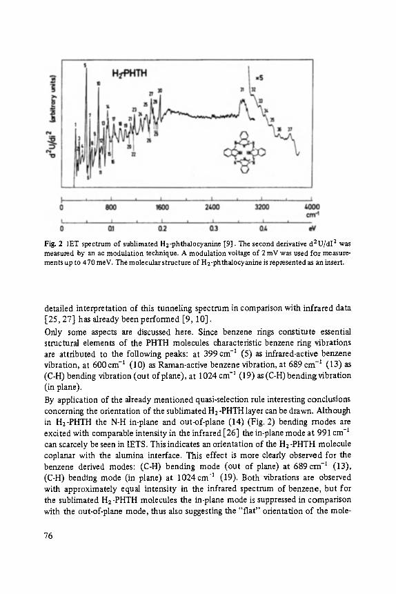
Fig. 2 IET spectrum of sublimated H2-phthalocyanine [9]. The second derivative d2U/dl 2 was measured by an ac modulation technique. A modulation voltage of 2 mV was used for measure- ments up to 470 meV. The molecular structure of H2-phthalocyanine is represented as an insert.
detailed interpretation of this tunneling spectrum in comparison with infrared data [25, 27] has already been performed [9, 10].
Only some aspects are discussed here. Since benzene rings constitute essential structural elements of the PHTH molecules characteristic benzene ring vibrations are attributed to the following peaks: at 399 crn -1 (5) as infrared-active benzene vibration, at 600 cm -1 (10) as Raman-active benzene vibration, at 689 cm -I (13) as (C-H) bending vibration (out of plane), at 1024 cm -1 (19) as (C-H) bending vibration (in plane).
By application of the already mentioned quasi-selection rule interesting conclusions concerning the orientation of the sublimated H2 -PHTH layer can be drawn. Although in H2-PHTH the N-H in-plane and out-of-plane (14) (Fig. 2) bending modes are excited with comparable intensity in the infrared [26] the in-plane mode at 991 cm -~ can scarcely be seen in IETS. This indicates an orientation of the H2-PHTH molecule coplanar with the alumina interface. This effect is more clearly observed for the benzene derived modes: (C-H) bending mode (out of plane) at 689 em -~ (13), (C-H) bending mode (in plane) at 1024cm -I (19). Both vibrations are observed with approximately equal intensity in the infrared spectrum of benzene, but for the sublimated H2-PHTH molecules the in-plane mode is suppressed in comparison with the out-of-plane mode, thus also suggesting the "flat" orientation of the mole-
76
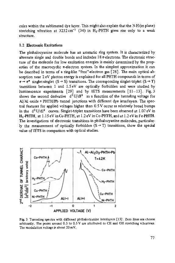
cules within the sublimated dye layer. This might also explain that the N-H (in plane) stretching vibration at 3232cm -1 (34) in H2-PHTH gives rise only to a weak structure.
1.2 Electronic Excitations
The phthalocyanine molecule has an aromatic ring system. It is characterized by alternate single and double bonds and includes 187r-electrons. The electronic struc- ture of the molecule for low excitation energies is mainly determined by the prop- erties of the macrocyclic n-electron system. In the simplest approximation it can be described in terms of a ring-like "free"-electron gas [28]. The main optical ab- sorption near 2 eV photon energy is explained for all PHTH compounds in terms of 7r ~ zr* singlet-singlet (S ~ S) transitions. The corresponding singlet-triplet (S ~ T) transitions between 1 and 1.5 eV are optically forbidden and were studied by luminescence experiments [29] and by lETS measurements [11-13] . Fig. 3 shows the second derivative d 2 U/dI 2 as a function of the tunneling voltage for M/M oxide + PHTH/Pb tunnel junctions with different dye inteflayers. The spec- tral features for applied voltages higher than 0.5 V occur as relatively broad bumps in the d2U/dI 2 curves. Singlet-triplet transitions have been observed at 1.07 eV in H2 -PHTH, at 1.15 eV in Cu-PHTH, at 1.2 eV in Co-PHTH, and at 1.2 eV in Fe-PHTH. The investigations of electronic transitions in phthalocyanine molecules, particular- ly the measurement of optically forbidden (S ~ T) transitions, show the special value of lETS in comparison with optical studies.
Fig. 3 Tunneling spectra with different phthalocyanine interlayers [13]. Zero lines are chosen arbitrarily. The peaks around 0.3 to 0.5 V are attributed to CH and OH stretching vibrations. The modulation voltage is about 20 inV.
77
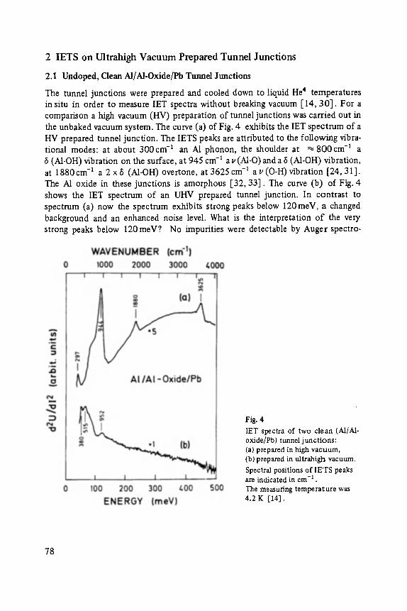
2 I E T S on Ul t r ah igh V a c u u m P r e p a r e d T u n n e l J u n c t i o n s
2.1 Undoped, Clean Al/AI-Oxide/Pb Tunnel Junctions
The tunnel junctions were prepared and cooled down to liquid He 4 temperatures in situ in order to measure IET spectra without breaking vacuum [14, 30] . For a comparison a high vacuum (HV) preparation of tunnel junctions was carried out in the unbaked vacuum system. The curve (a) of Fig. 4 exhibits the IET spectrum of a HV prepared tunnel junction. The IETS peaks are attributed to the foUowing vibra- tional modes: at about 300crn -1 an A1 phonon, the shoulder at ~ 8 0 0 c m -1 a 8 (AI-OH) vibration on the surface, at 945 cm -1 a u (?d-O)and a ~ (AI-OH) vibration, at 1880cm -1 a 2 x ~ (M-OH) overtone, at 3625 crn -1 a u (O-H) vibration [24, 31]. The A1 oxide in these junctions is amorphous [32, 33]. The curve (b) of Fig. 4 shows the IET spectrum of an UHV prepared tunnel junction. In contrast to spectrum (a) now the spectrum exhibits strong peaks below 120meV, a changed background and an enhanced noise level. What is the interpretation o f the very strong peaks below 120meV? No impurities were detectable by Auger spectro-
Fig. 4 lET spectra of two clean (AI/A1- oxide/Pb) tunnel junctions: (a) prepared in high vacuum, (b) prepared in ultrahigh vacuum. Spectral positions of IETS peaks are indicated in cm -1 . The measuring temperature was 4.2 K [14].
78
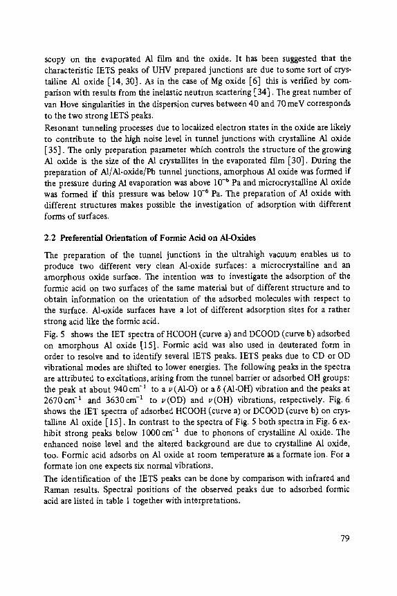
scopy on the evaporated AI film and the oxide. It has been suggested that the characteristic IETS peaks of UHV prepared junctions are due to some sort of crys- talline A1 oxide [ 14, 30]. As in the case of Mg oxide [6] this is verified by com- parison with results from the inelastic neutron scattering [34]. The great number of van Hove singularities in the dispersion curves between 40 and 70 meV corresponds to the two strong lETS peaks.
Resonant tunneling processes due to localized electron states in the oxide are likely to contribute to the high noise level in tunnel junctions with crystalline A1 oxide [35]. The only preparation parameter which controls the structure of the growing A1 oxide is the size of the A1 crystaUites in the evaporated film [30]. During the preparation of A1/Al-oxide/Pb tunnel junctions, amorphous A1 oxide was formed if the pressure during A1 evaporation was above 10 -o Pa and microcrystalline A1 oxide was formed if this pressure was below 10 -4 Pa. The preparation of A1 oxide with different structures makes possible the investigation of adsorption with different forms of surfaces.
2.2 Preferential Orientation of Formic Acid on M-Oxides
The preparation of the tunnel junctions in the ultrahigh vacuum enables us to produce two different very clean Al-oxide surfaces: a microcrystalline and an amorphous oxide surface. The intention was to investigate the adsorption of the formic acid on two surfaces of the same material but of different structure and to obtain information on the orientation of the adsorbed molecules with respect to the surface. N-oxide surfaces have a lot of different adsorption sites for a rather strong acid like the formic acid.
Fig. 5 shows the lET spectra of HCOOH (curve a) and DCOOD (curve b) adsorbed on amorphous A1 oxide [15]. Formic acid was also used in deuterated form in order to resolve and to identify several IETS peaks, lETS peaks due to CD or OD vibrational modes are shifted to lower energies. The following peaks in the spectra are attributed to excitations, arising from the tunnel barrier or adsorbed OH groups: the peak at about 940 cm -l to a v(A1-O) or a ~ (N-OH) vibration and the peaks at 2670cm -1 and 3630cm -1 to v(OD) and v(OH) vibrations, respectively. Fig. 6 shows the lET spectra of adsorbed HCOOH (curve a) or DCOOD (curve b) on crys- talline A1 oxide [ 15]. In contrast to the spectra of Fig. 5 both spectra in Fig. 6 ex- hibit strong peaks below 1000cm -1 due to phonons of crystalline A1 oxide. The enhanced noise level and the altered background are due to crystalline AI oxide, too. Formic acid adsorbs on A1 oxide at room temperature as a formate ion. For a formate ion one expects six normal vibrations.
The identification of the lETS peaks can be done by comparison with infrared and Raman results. Spectral positions of the observed peaks due to adsorbed formic acid are listed in table 1 together with interpretations.
79
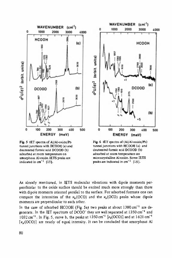
Fig. 5 lET spectra of A1/Al-oxide/Pb tunnel junctions with HCOOH (a) and deuterated formic acid DCOOD (b) adsorbed at room temperature on amorphous M-oxide. lETS peaks are indicated in cm -1 [15].
Fig. 6 IET spectra of (Al/Al-oxide/Pb) tunnel junctions with HCOOH (a) and deuterated formic acid DCOOD (b) adsorbed at room temperature on microcrystalline M-oxide. Some IETS peaks are indicated in cm -1 [15].
As already mentioned, in lETS molecular vibrations with dipole moments per- pendicular to the oxide surface should be excited much more strongly than those
with dipole moments oriented parallel to the surface. For adsorbed formate one can compare the intensities of the va(OCO) and the vs(OCO ) peaks whose dipole
moments are perpendicular to each other.
In the case of adsorbed HCOOH (Fig. 5a) two peaks at about 1380cm -1 are de-
generate. In the IET spectrum of DCOO- they are well separated at 1350 cm -1 and
1032cm -1 . In Fig. 5, curve b, the peaks at 1350cm -1 [vs(OCO)] and at 1621 cm -1 [va(OCO)] are nearly of equal intensity. It can be concluded that amorphous A1
80

Table 1 Comparison of spectral positions (in crn - t ) of lETS peaks with infrared (IR) data (on formic acid adsorbed on -r-Al-oxide) and Rarnan (Ra) data (on crystalline formate). The type and the form of normal vibrations are represented. ( , : approximated peak position [15 ].
wQvenumbers crn -I
HCOO" type form IR Ra lETS
'v s (OCOI 1390 1352 1370
& 2915 2825 289/, v (CH)
o(oco} I ~ 769 773 788 vo (OCO) ~,~ 1625 158/. 1629
5 (CH) ~j~ 1/,07 1386 1392
1r (CH) ~ . . 1062 1069 1061
OCO0-
IR Ra IETS
1385 1329 1350
2220 2122 2169
762 I 757
1625 1579
1029 1029
912 918
7901"|
1621
1032
887 1
oxide offers a lot of different adsorption sites, where formic acid adsorbs in a rather random manner,
In tunnel junctions with crystalline A1 oxide the spectrum with DCOO- (Fig. 6, curve b) shows that the vs(OCO ) peak at 1360cm -1 is stronger than the va(OCO) peak at 1610cm -1 [15]. Microcrystalline A1 oxide offers a smaller but more homogeneous population of adsorption sites where the formate ions adsorb with a preferred orientation.
3 Compar isons be tween IETS and o t h e r Surface Vibrat ional Spec t roscopies
The examples and applications discussed here have shown that the IETS is well suited for the investigation of surface vibrational properties. This point will be explored in more detail. Vibrational spectroscopy is an important tool to charac- terize an adsorbate-substrate system. In the following the IETS will be compared
with other methods of surface vibrational spectroscopy: the Infrared Reflection Absorption Spectroscopy (IRAS) [36, 37], the High Resolution Electron Energy Loss Spectroscopy (HREELS) [39] and the Surface Enhanced Raman Spectroscopy (SERS) [40]. A summary of these techniques is presented in table 2. The advantage of IETS is the good resolution and the sensitivity. Approximately 10 -2 monolayer of
81
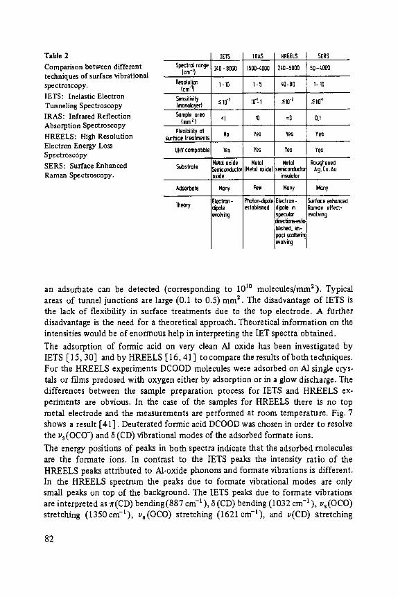
Table 2 Comparison between different Spectral range techniques of surface vibrational (cm'l)
Res~ut~ spectroscopy. (cm-~)
lETS: Inelastic Electron ~sitivily Tunneling Spectroscopy (monaoyer)
IRAS: Infrared Reflection Sample area Absorption Spectroscopy (nurz)
Flexibility at HREELS: High Resolution surloce treatments
Electron Energy Loss UHY compatible Spectroscopy SERS: Surface Enhanced 5ubstmte Raman Spectroscopy.
~'sod~te
Theory
2t, O - 8O00 1500-t, OOO
1 -I0 1-5
< 10 z 1fiLl
<I 10
No Yes
Yes Yes
Nelol oxide Hetnl ~*tmcor~ductor (Metal oxide] oxide
Nony Few
SERS
2t.O -5000 50-t,099
t,O- 80 1-10
_<lo-z <10 -1
=3 0.1
Yes Yes
Yes Yes
Metal Roughened ;emk:ortduchx Ag.Eu.Au
insulator
Nany Nany
Electron- S~'foce enhanced dipole n Raman effect- s P ~ t c - ~~
~ished. im- p o c t ~ ~volv~ I
an adsorbate can be detected (corresponding to 101~ molecules/mm2). Typical areas of tunnel junctions are large (0.1 to 0.5) mm 2. The disadvantage of IETS is the lack of flexibility in surface treatments due to the top electrode. A further disadvantage is the need for a theoretical approach. Theoretical information on the intensities would be of enormous help in interpreting the IET spectra obtained.
The adsorption of formic acid on very clean A1 oxide has been investigated by IETS [ 15, 30] and by HREELS [ 16, 41] to compare the results of both techniques. For the HREELS experiments DCOOD molecules were adsorbed on A1 single crys- tals or f'flms predosed with oxygen either by adsorption or in a glow discharge. The differences between the sample preparation process for IETS and HREELS ex- periments are obvious. In the case of the samples for HREELS there is no top metal electrode and the measurements are performed at room temperature. Fig. 7 shows a result [41]. Deuterated formic acid DCOOD was chosen in order to resolve the vs(OCO- ) and ~ (CD) vibrational modes of the adsorbed formate ions.
The energy positions of peaks in both spectra indicate that the adsorbed molecules are the formate ions. In contrast to the IETS peaks the intensity ratio of the HREELS peaks attributed to Al-oxide phonons and formate vibrations is different. In the HREELS spectrum the peaks due to formate vibrational modes are only small peaks on top of the background. The IETS peaks due to formate vibrations are interpreted as 7r(CD) bending (887 cm -1 ), 8 (CD) bending (1032 cm -1 ), v s (OCO) stretching (1350cm-1), va(OCO) stretching (1621cm-1), and v(CD) stretching
82
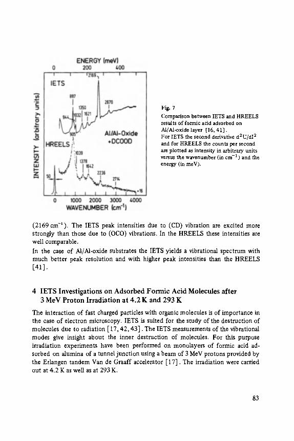
Fig. 7 Comparison between IETS and HREELS results of formic acid adsorbed on Al/Al-oxide layer [16, 41]. For IETS the second derivative dZU/dI 2 and for HREELS the counts per second are plotted as intensity in arbitrary units versus the wavenumber (in cm- t ) and the energy (in meV).
(2169 cm-~ ). The IETS peak intensities due to (CD) vibration are excited more strongly than those due to (OCO) vibrations. In the HREELS these intensities are well comparable.
In the case of A1/Al-oxide substrates the IETS yields a vibrational spectrum with much better peak resolution and with higher peak intensities than the HREELS [41].
4 IETS Invest igat ions on Adsorbed Fo rmic Acid Molecules af ter
3 MeV Pro ton I r radia t ion at 4 .2 K and 293 K
The interaction of fast charged particles with organic molecules is of importance in the case of electron microscopy. IETS is suited for the study of the destruction of molecules due to radiation [ 17, 42, 43]. The IETS measurements of the vibrational modes give insight about the inner destruction of molecules. For this purpose irradiation experiments have been performed on monolayers of formic acid ad- sorbed on alumina of a tunnel junction using a beam of 3 MeV protons provided by the Erlangen tandem Van de Graaff accelerator [ 17]. The irradiation were carried out at 4.2 K as well as at 293 K.
83
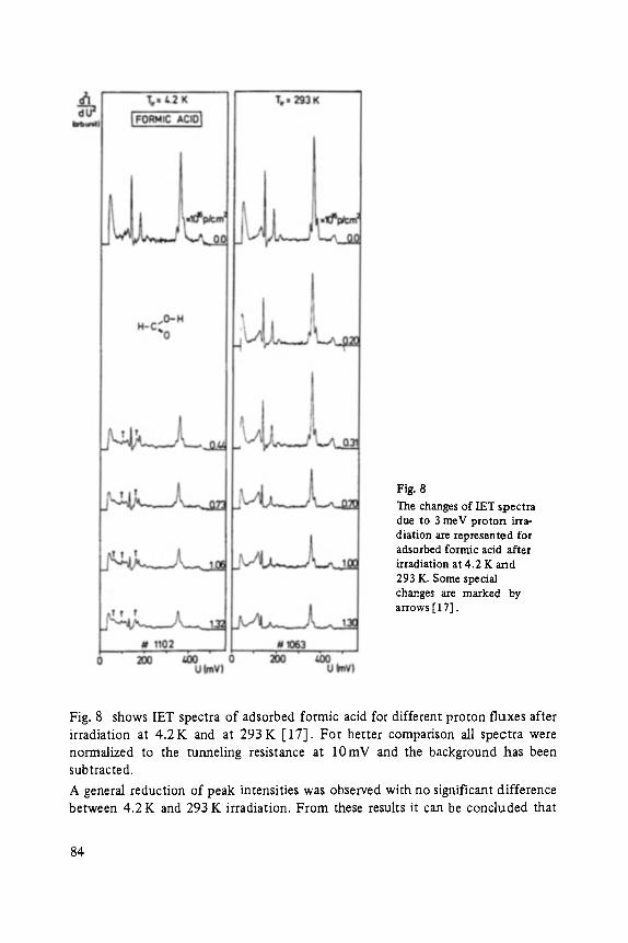
Fig. 8 The changes of IET spectra due to 3 meV proton irra- diation are represented for adsorbed formic acid after irradiation at 4.2 K and 293 K. Some special changes are marked by arrows [17].
Fig. 8 shows IET spectra of adsorbed formic acid for different proton fluxes after irradiation at 4.2K and at 293 K [17]. For better comparison all spectra were normalized to the tunneling resistance at 10mV and the background has been subtracted.
A general reduction of peak intensities was observed with no significant difference between 4.2 K and 293 K irradiation. From these results it can be concluded that
84
the origin of cryoprotection observed in the electron microscopy is mostly due to a reduction of atomic mobility. The IET spectra after low temperature irradiation exhibit some special changes marked by arrows in Fig. 8. Probably the new peaks arise from molecular fragments formed after irradiation. These fragments only stick on the interface at low temperatures and are therefore not present in spectra taken after irradiation at 293 K [ 17].
5 Tunne l ing S p e c t r o s c o p y on n-Si /S iO2/Meta l S t ruc tures wi th
Very Th in SiO2 F i lms
The aim of the following investigations is the detection and characterization of impurities and interface states in MOS structures with very thin Si oxide. The interface states cause a considerable excess direct current and a large frequency dispersion of the capacitance and the conductance curves.
Electron tunneling spectroscopy is used for the investigation of n-Si/SiO2/metal tunnel junctions with very thin SiO: films (1-3 nm) to obtain information about phonons or impurities in the SiO2 interlayer or at the Si-SiO2 interface. Especially, the measurements of vibrational modes of the doping materials and uncontrolled contaminations offer the possibility to detect such impurities. Additionally, from measurements of tunneling conductivity information can be obtained about tl'/e density of states near the Si-SiO2 interface. The transport mechanism in the junc- tion is tested to be mainly due to tunneling by measuring the energy gap of a super- conducting metal electrode.
5.1 Sample Preparation
Boron-doped silicon wafers ((100) oriented, resistivity p = 0 .8-1 .2 ~2 cm, boron concentration n B = 1.5 "1016 cm -3, dimensions 18 x 12 x 1 mm 3) serve as a sub- strate. For the tunneling measurements at 4.2 K two degenerate phosphorus-doped Si-layers (10 • 0.7 • 0.002 mm 3 , n = 5" 1020 phosphorus atoms cm -3) are prepared [18].
The oxidation of the n-Si layer is performed in dry oxygen at 600 ~ for 6 minutes. Evaporated AI trims (annealed in a nitrogen atmosphere at 400 ~ 20 minutes) are used for ohmic contacts. Finally the top metal electrode (Pb or Ag) is evaporated. In this way two tunnel structures are produced on the same substrate. The second tunnel junction is used for comparison.
5.2 Results and Discussion
Fig. 9 exhibits the tunneling resistance dU/dI as a function of the applied tunneling voltage for an n-Si/SiO2/Pb and for an n-Si/SiO2/Ag tunnel junction. In the case of positive polarity electrons tunnel from the semiconductor into the metal. Strong structures around U = 0 are observed due to the superconductivity of lead. Also
85
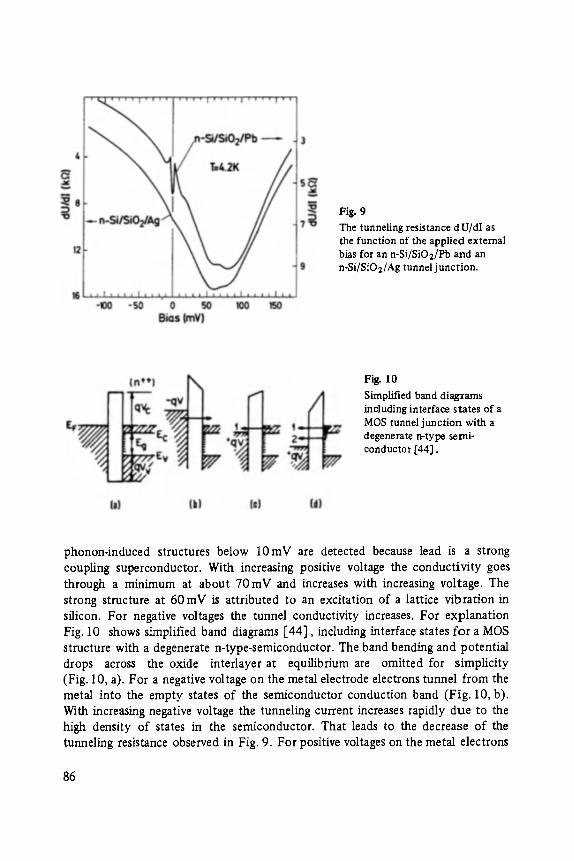
Fig. 9 The tunneling resistance dU/dI as the function of the applied external bias for an n-Si/SiO2/Pb and an n-Si/SiO2/Ag tunnel junction.
F~. l0 Simplified band diagxams including interface states of a MOS tunnel junction with a degenerate n-type semi- conductor [44].
phonon-induced structures below lOmV are detected because lead is a strong coupling superconductor. With increasing positive voltage the conductivity goes through a minimum at about 7 0 m V and increases with increasing voltage. The strong structure at 60 mV is attributed to an excitation of a lattice vibration in silicon. For negative voltages the tunnel conductivity increases. For explanation Fig. 10 shows simplified band diagrams [44] , including interface states fo r a MOS structure with a degenerate n-type-semiconductor. The band bending and potential drops across the oxide interlayer at equilibrium are omitted for simplicity (Fig. 10, a). For a negative voltage on the metal electrode electrons tunnel from the metal into the empty states of the semiconductor conduction band (Fig. 10, b). With increasing negative voltage the tunneling current increases rapidly due to the high density of states in the semiconductor. That leads to the decrease of the tunneling resistance observed in Fig. 9. For positive voltages on the metal electrons
86
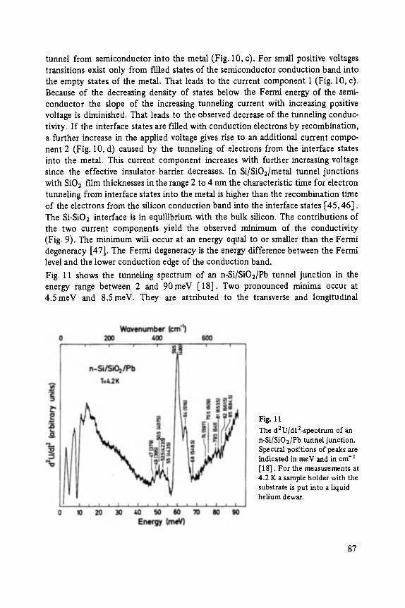
tunnel from semiconductor into the metal (Fig. 10, c). For small positive voltages transitions exist only from fiUed states of the semiconductor conduction band into the empty states of the metal. That leads to the current component 1 (Fig. 1 O, c). Because of the decreasing density of states below the Fermi energy of the semi- conductor the slope of the increasing tunneling current with increasing positive voltage is diminished. That leads to the observed decrease of the tunneling conduc- tivity. If the interface states are filled with conduction electrons by recombination, a further increase in the applied voltage gives rise to an additional current compo- nent 2 (Fig. 10, d) caused by the tunneling of electrons from the interface states into the metal. This current component increases with further increasing voltage since the effective insulator barrier decreases. In Si/SiO2/metal tunnel junctions with SiO2 film thicknesses in the range 2 to 4 nm the characteristic time for electron tunneling from interface states into the metal is higher than the recombination time of the electrons from the silicon conduction band into the interface states [45,46]. The Si-SiO2 interface is in equilibrium with the bulk silicon. The contributions of the two current components yield the observed minimum of the conductivity (Fig. 9). The minimum will occur at an energy equal to or smaller than the Fermi degeneracy [47]. The Fermi degeneracy is the energy difference between the Fermi level and the lower conduction edge of the conduction band.
Fig. 11 shows the tunneling spectrum of an n-Si/SiO2/Pb tunnel junction in the energy range between 2 and 90meV [18]. Two pronounced minima occur at 4.5 meV and 8.5 meV. They are attributed to the transverse and longitudinal
Fig. 11 The d2U/dI2-spectrum of an n-Si/SiO2/Pb tunnel junction. Spectral positions of peaks are indicated in meV and in era- i [18]. For the measurements at 4.2 K a sample holder with the substrate is put into a liquid helium dewar.
87

Fig. 12 The d2U/dlZ-spectrum of an n-Si/SiO2/Ag tunnel junction. A moldulation voltage of 1 mV was used [18]. A multichannel analyser improved the signal to noise ratio [18].
acoustic phonons of the superconducting lead due to phonon-induced structure in the electronic density of states [48]. Additional lead-phonon structure arising from multiple-phonon processes can be observed at about 13.5 meV and 16.5 meV.
Fig. 12 shows the IET spectrum of an n-Si/SiO2/Ag tunnel junction in the energy range 0 to 180 meV. In the following both spectra (Figs. 11 and 12) are interpreted and discussed. Essential points of the discussion can be seen in comparison with infrared data [49-53] on silicon and silicon oxide and with previous tunneling measurements on MOS structures [47, 54-61] .
The following peaks are attributed to excitations of Si lattice vibrations: the strong peak at 60 meV is due to TO phonon (L-point) [56,57,62,63], the peak at 64 meV is due to LO and TO phonon (F-point) [57, 62, 63], and the weak peak at 50.5 meV is due to LA and LO phonon (X-point).
In the spectrum of the n-Si/SiO2/Ag tunnel junction (Fig. 12) at low energies the peaks at 12.5 meV, 25 meV, and 43 meV are attributed to a TA phonon (L-point), a TA phonon (K-point), and a LA phonon (K-point). Peaks at 52.5 meV and 55 meV (Fig. 11) are interpreted as excitations of a (Si-P) and a (Si-O) vibrational mode [52]. According to infrared data a Si-O vibrational mode at 133 meV has been detected [52]. The peak at 127 meV (Fig. 12) is inter- preted tentatively as an excitation of a (Si-O) vibration.
88
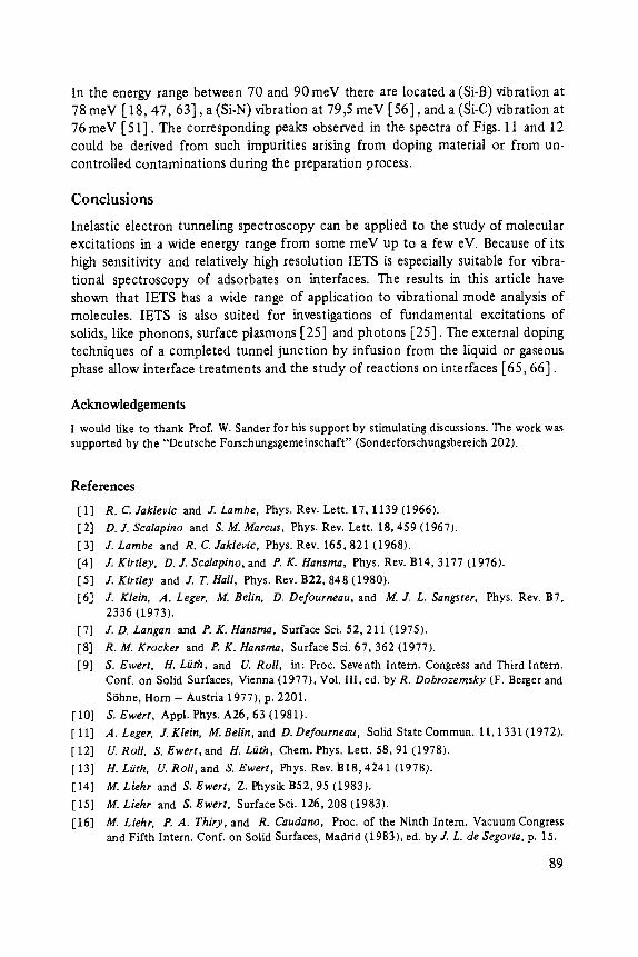
In the energy range between 70 and 90 meV there are located a (Si-B) vibration at 78 meV [ 18, 47, 63], a (Si-N) vibration at 79,5 meV [56], and a (Si-C) vibration at 76 meV [51]. The corresponding peaks observed in the spectra of Figs. 11 and 12 could be derived from such impurities arising from doping material or from un- controlled contaminations during the preparation process.
Conclusions
Inelastic electron tunneling spectroscopy can be applied to the study of molecular excitations in a wide energy range from some meV up to a few eV. Because of its high sensitivity and relatively high resolution lETS is especially suitable for vibra- tional spectroscopy of adsorbates on interfaces. The results in this article have shown that lETS has a wide range of application to vibrational mode analysis of molecules, lETS is also suited for investigations of fundamental excitations of solids, like phonons, surface plasmons [25] and photons [25]. The external doping techniques of a completed tunnel junction by infusion from the liquid or gaseous phase allow interface treatments and the study of reactions on interfaces [65, 66].
Acknowledgements
[ would like to thank Prof. W. Sander for his support by stimulating discussions. The work was supported by the "Deutsche Forschungsgemeinschaft" (Sonderforschungsbereich 202).
References
[1] R.C. Jaklevic and J. Lambe, Phys. Rev. Lett. 17, 1139 (1966).
[2] D.J. Scalapino and S. M. Marcus, Phys. Roy. Lett. 18,459 (1967).
[3] J. Lambe and R. C. Jaklevic, Phys. Roy. 165,821 (1968).
[4] J. Kirtley, D. J. Scalapino, and P. K. Hansma, Phys. Rev. BI4, 3177 (1976).
[5] J. Kirtley and J. T. Hall, Phys. Rev. B22, 848 (1980).
[6] 3". Klein, A. Leger, M. Belin, D. Defourneau, and M. J. L. Sangster, Phys. Rev. B7, 2336 (1973).
[7] J.D. Langan and P. K. Hansma, Surface Sci. 52,211 (1975).
[8] R.M. Krocker and P. K. Hansma, Surface Sci. 67, 362 (1977).
[9] S. Ewert, 1"1. Liirh, and U. Roll, in: Proc. Seventh Intern. Congress and Third Intern. Conf. on Solid Surfaces, Vienna (1977), Vol. III, ed. by R. Dobrozemsky (F. Berger and
S6hne, Horn - Austria 1977), p. 2201.
[10] S. Ewert, Appl. Phys. A26, 63 (1981).
[ 11] A. Leger, J. Klein, M. Belin, and D. Defourneau, Solid State Commun. 11, 1331 (i 972).
[12] U. RolI, S. Ewerr, and H. Liith, Chem. Phys. Lett. 58,91(1978) .
[13] H. Liith, U. Roll, and S. Ewert, Phys. Rev. B18,4241(1978).
[14] M. Liehr and S. Ewert, Z. PhysikB52,95(1983) .
[ 15] M. Liehr and S. Ewert, Surface Sci. 126,208 (1983).
[16] M. Liehr, P. A. Thiry, and R. Caudano, Proc. of the Ninth Intern. Vacuum Congress and Fifth Intern. Conf. on Solid Surfaces, Madrid (1983), ed. by J. L. de Segovia, p. 15.
89
[17] R. Behrle, IV. R6sner, tt. Adrian, G. Saemann-lschenko, F. B6mmel, and L. S61dner, in: Proc. of the Tenth Intern. Conf. on Atomic Collisions in Solids (1983), Bad Iburg (North Holland Physics Publishing Division).
[18] P. Balk, H.-G. Busmann, S. Ewert, K. Seibert, and A. Steffen, to be published.
[19] N.M. Brown and D. G. Ivalmsley, Chem. Br. 12,92(1976). [20] R.G. Keil, T.P. Graham, and K.P. Roenker, Appl. Spectrosc. 30, 1 (1976).
[21] P.K. Hansma, Phys. Rep. 30C, 146 (1977). [22] E.L. Wolf, Rep. Prog. Phys. 41, 1439 (1978). [23] C. Hamann and S. Trompler, Exp. Techn. Phys. 26,241 (1978). [24] T. Wolfram (ed.), Inelastic Electron Tunneling Spectroscopy, Springer Series in Solid
State Sci. 4 (Springer, Berlin - Heidelberg - New York 1978). [25] P. K. Hansma (ed.), Tunneling Spectroscopy (Plenum Press, New York and London,
1982). [26] T. KobayashL F. Kurokawa, N. Yeda, and E. Suito, Spectrochim. Acta 26A, 1305
(1970). [27] T. Kobayashi, Spectrochim. Acta 26A, 1313 (1970). [28] H. Kuhn, J. Chem. Phys. 17,1198 (1949) andAng. Chem. 71, 93 (1959). [29] P. S. Vincett, E. M. Voigt, and K. E. Rieckhoff, J. Chem. Phys. 55, 4131 (1971).
[30] M. Liehr, Thesis, RWTH Aachen, F.R.G. (1982). [ 31] IV. M. Bowser and IV. H. Iveinberg, Surface Sci. 64,377 (1977). [32] J. IV. Diggle, T. C. Downie, and C. IV. Goulding, Chem. Rev. 69, 365 (1969). [33] J. Chatelet, H. H. Claasen, D. M. Gruen, I. Shell, and R. B. Ivright, Appl. Spectrosc.
29, 185 (1975). [34] H. Bialas and ['1. J. Stolz, Z. Physik B21,319 (1975).
[35] J. Halbritter, Surface Sci. 122, 80 (1982). [36] J. Pritchard, T. Catterick, and R. K. Gupta, Surface Sci. 53, 1 (1975).
[37] R.A. Shigeishi and D. A. King, Surface Sci. 58,379 (1976).
[38] H.J. Krebs and H. Lath, Appl. Phys. 14,337 (1977). [39] H. [bach, Phys. Rev. Lett. 24, 1416 (1970) and Phys. Rev. Lett. 27, 253 (1971). [40] M. Fleischmann, P. U. Hendra, and A.J. McQuillan, Chem. Phys. Lett. 26, 1630 (1974).
R. P. van Duyne, in: Chemical and Biochemical Applications of Lasers, ed. C. B. Moore, 4,101 Academic Press, New York (1979). R. Dornhaus, Festk6rperprobleme 22,201 (1982), ed. P. Grosse, Vieweg, Braunschweig.
[41] M. L iehr, P. A. Thiry , and R. Caudano, to be published. [42] J. T. Hall, P. K. Hansma, and M. Parikh, Surface Sci. 65,552 (1977).
[43] J.M. Clark and R. V. Coleman, J. Chem. Phys. 73, 2156 (1980). [44] IV. E. Dahlke and S. M. Sze, Solid State Electronics 10, 865 (1967).
S. hi. Sze, Physics of Semiconductor Devices, Bell Laboratories, Wiley-Interseience Publication, 1981.
[45] L.B. Freeman and IV. E. Dahlke, Solid State Electronics 13, 1483 (1970).
[46] S. Kar and IV. E. Dahlke, Solid State Electronics 15,221 (1972).
[47] D.E. Cullen, E.L. IVolf, and IV. D. Compton, Phys. Rev. B2, 3157 (1970). [48] IV. L. McMillan and J. M. Rowell, Superconductivity, Vol. I, Chap. 11, ed. by R. D.
Parks, Marcel Dekker, New York 1969.
90

[49] H.J. Hrostowski and R. H. Kaiser, Phys. Rev. 107,966 (1957).
[50] S.D. Smith and J. F. Angress, Physics Lett. 6,131 (1963).
[51] R.C. Newman and J.B. Willis, J. Phys. Chem. Solids 26,373 (1965).
[52] G. Ir Anderson, W.A. Schmidt, and J. Comas, J. Electrochem. Soc.: Solid State Science and Technology 125,424 (1978).
[53] Ir A. Pliskin, Semiconductor Silicon 1973, 2 nd Intern. Symposium on Silicon Materials Science and Technology, 1973, Chicago, ed. by Howard Huff.
[54] E.L. Wolf, Phys. Rev. Lett. 20, 204 (1968).
[55] L.C. Davis and C. B. Duke, Phys. Rev. 184,764 (1969).
[56] L.B. Schein and Ir D. Compton, Appl. Phys. Lett. 17,236 (1970).
[57] D.C. Tsui and L. N. Dunkleberger, Appl. Phys. Lett. 18, 200 (1971).
[58] E.L. Wolf, Solid State Physics 30, 2 (1975), ed. by H. Ehrenreich, Academic Press, New York, San Francisco, London.
[59] A . F . J . Levi, W. A. Phillips and C. J. Adkins, Solid State Commun. 45, 43 (1983).
[60] J. Nishizawa and M. Kimura, Japanese Journal of Applied Physics 14, 1529 (1975).
[61] M. C. Payne and J. C. Inkson, J. Phys. C: Solid State Physics 16, 4259 (1983).
[62] B.N. Brockhouse, Phys. Rev. Lett. 2, 256 (1959).
[63] M. Pepper, Solid State Physics 13, L 709 (1980).
[64] M. Balkanski and Ir Nazarewicz, J. Phys. Chem. Solids 27,671 (1965).
[65] R.C. Jaklevic and ill. R. Gaerttner, Appl. Phys. Lett. 30, 646 (1977).
[66] R. C. Jaklevic and M. R. Gaerttner, Appl. Surf. Sci. 1,479 (1978).
91
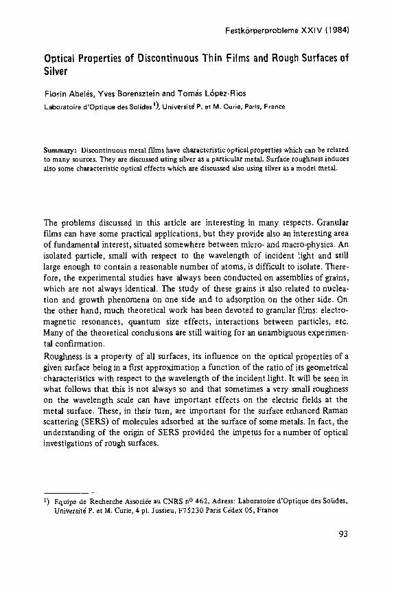
Festk6rperprobleme XXIV (1984)
Optical Properties of Discontinuous Thin Films and Rough Surfaces of Silver
Florin Abelds, Yves Borensztein and Tom~s L6pez-Rios
Laboratoire d'Optique des Solides 1), Universitd P. et M. Curie, Paris, France
Summary: Discontinuous metal films have characteristic optical properties which can be related to many sources. They are discussed using silver as a particular metal. Surface roughness induces also some characteristic optical effects which are discussed also using silver as a model metal.
The problems discussed in this article are interesting in many respects. Granular films can have some practical applications, but they provide also an interesting area of fundamental interest, situated somewhere between micro- and macro-physics. An isolated particle, small with respect to the wavelength of incident light and still large enough to contain a reasonable number of atoms, is difficult to isolate. There- fore, the experimental studies have always been conducted on assemblies of grains, which are not always identical. The study of these grains is also related to nuclea- tion and growth phenomena on one side and to adsorption on the other side. On the other hand, much theoretical work has been devoted to granular films: electro- magnetic resonances, quantum size effects, interactions between particles, etc. Many of the theoretical conclusions are still waiting for an unambiguous experimen- tal confirmation.
Roughness is a property of all surfaces, its influence on the optical properties of a given surface being in a first approximation a function of the ratio of its geometrical characteristics with respect to the wavelength of the incident light. It will be seen in what follows that this is not always so and that sometimes a very small roughness on the wavelength scale can have important effects on the electric fields at the metal surface. These, in their turn, are important for the surface enhanced Raman scattering (SERS) of molecules adsorbed at the surface of some metals. In fact, the understanding of the origin of SERS provided the impetus for a number of optical investigations of rough surfaces.
1) Equipe de Recherche Associ~e au CNRS n ~ 462, Adress: Laboratoire d 'Optique des Solides, Universitd P. et M. Curie, 4 pl. Jussieu, F75230 Paris Cddex 05, France
93

The points discussed here are, at first sight, of two different types. The first con- cerns granular or discontinuous f'flms, whereas the other deals with surface roughness. Both problems have already been discussed separately. Our aim is to bring them together in order to show that there might be some connexions between them. Although these relations are not very striking at first sight, they will appear in due course. We discuss metallic materials only and, more specifically, silver. For semi- conductors, surface roughness is quite often described now by a thin layer, with dielectric constant computed by using an effective medium theory and assuming that the rough region is made out of a mixture of the semiconductor and the embed- ding medium.
The paper has been organized mainly to give an overview of the present situation. For this reason, our own results are not given a special pre-eminence.
I Discon t inuous Silver Thin Fi lms
1 I n t r o d u c t i o n
It has been known for a long time that extremely thin metal films present colours that are usually different from the colours of the bulk metal. As early as 1857, Faraday proposed that this phenomenon should be ascribed to their aggregated nature. This conjecture has since been confirmed, and in the last decades many investigations have shown that discontinuous silver fihns or, more generally, systems of silver particles present a so-called abnormal absorption [1-13]. Early in this century, Mie [14] gave a rigorous solution of the problem of light scattering and light absorption by homogeneous spherical particles situated in an homogeneous medium, in terms of classical electromagnetic theory. In this treatment, the spheres are assumed to be large enough for the macroscopic dielectric theory to be appli- cable, with no other limitation on their size. When the wavelength of light is much smaller than the dimension of the particles and the distance between them, the quasistatic approximation can be employed, and the optical properties o f the metal particles can be characterized by an effective medium, as it was first developed by Maxwell Garnett [15] in 1904 for spherical particles, then by David [16] in 1937 for spheroidal particles.
In this section, after discussing the experimental procedures for the sample pre- paration and their characterization, we shall study the so-called plasma resonances. Absorption in isolated metal particles, then in discontinuous films treated within the effective medium theories, will be compared with experimental results. The case of very thin discontinuous films, where quantum size effects may occur, will be tackled. Finally, the influence of the particle size on the interband transitions will be discussed.
94
2 Prepa ra t ion o f D i scon t inuous F i lms
A large number of techniques has been used to prepare samples containing small metallic particles. Small particle systems include colloidal suspensions of the metals, gas-evaporated particles and cluster beams, colloidal particles contained in photo- sensitive glasses and metal dispersions in porous materials. In this paper we will discuss only the discontinuous thin films.
In the first stages of growth of vacuum deposited films, especially on amorphous substrates, many metals tend to form island4ike structures. The physical processes involved in the formation of metal clusters in the initial stages of thin f'rims have attracted much attention [43]. According to Schmeisser [44], the process of island growth may be described as follows: the metal atoms arriving at the substrate will be accommodated instantaneously, but the average time during which such a single atom will remain on the substrate is determined by the binding forces and the sub- strate temperature. In general, the threshold energy for changing sites on the sub- strate is much smaller than the energy of binding. Therefore, the single atom moves over the surface and may join an already existing cluster and therefore contribute to its growth. The particle diameter increases proportional to the square root of the amount of evaporated metal, and this leads to a size distribution which is theoreti- cally proportional to the diameter. Then coalescence of clusters is possible as a result of the mobility of the smaller clusters. The particle size may be influenced by chang- ing the substrate temperature. At higher temperature, but fixed evaporation rate, the nucleation rate decreases so that less particles are produced, the average diameter decreases and the overall efficiency of the metal deposition is reduced. Increase of the evaporation rate at fixed temperature causes a strong enhancement of the nu- cleation rate.
Most authors have prepared such silver discontinuous films by evaporating the metal on amorphous substrates like glass, fused quartz, polyvinyl alcohol, etc. We present here some results of the evaporation of silver onto an alumina substrate [45]. A continuous film of aluminium is exposed to several Langmuirs of oxygen (10 -4 torr during several minutes). Therefore, it becomes coated by an amorphous alumina film a few nanometers thick. Fig. 1 shows an electron transmission micrograph of a silver discontinuous film deposited on this substrate, maintained at room temper- ature, at a rate of about 0.05 nm/s. The average thickness is 2 nm. The large dark spots are disoriented aluminium cristallites. We clearly see two sets of silver parti- cles. The first one is composed of large islands of various shapes, some of them coa- lescing. The other set is composed of smaller particles, situated between the larger ones. The histogram, for this micrograph, in Fig. 2 shows the size distribution of the particles with two peaks centered around 3 nm and 9 nm corresponding respec- tively to the two sets of particles. It is still not clear whether there are successively two ensembles of nucleation sites or the growth of a part of the initial islands is stopped, while the other clusters continue to grow during evaporation of silver. The large clusters indicated on Fig. 2 (size higher than 12 nm) are due to the coa- lescence of two or more islands.
95
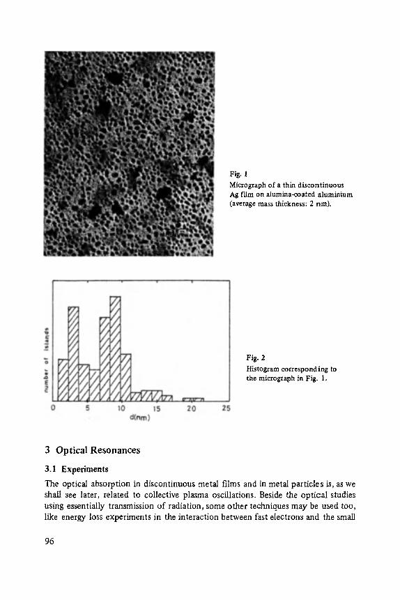
Fig. 1 Micrograph of a thin discontinuous Ag f'tlm on alumina-coated aluminium (average mass thickness: 2 rim).
Fig. 2 Histogram corresponding to the micrograph in Fig. I.
3 Op t i ca l R e s o n a n c e s
3.1 Experiments
The optical absorption in discontinuous metal films and in metal particles is, as we shall see later, related to collective plasma oscillations. Beside the optical studies using essentially transmission of radiation, some other techniques may be used too, like energy loss experiments in the interaction between fast electrons and the smaU
96
particles [17, 18], measurements of radiation spectra produced by this interaction [19], or direct observation of the scattered light [20, 21]. Here we are interested especially in optical experiments.
Figs. 3 and 4 show the opticaltransmittance with oblique incidence of silver disconti- nuous thin films of various thicknesses on silica, either in s-polarization or in p- polarization, after N. and A. Emetic [4]. With s-polarized incident radiation - i e. when the electric field vector is parallel to the film - the observed resonance~ let us call it the parallel one, is moving from about 3.2 eV to the infrared region with
Fig. 3 S-polarized light transmittance of dis- continuous silver films on glass substrate, with thicknesses ranging from 1 nm to 32 nm. From [4].
Fig. 4 P-polarized light transmittance for the same samples as in Fig. 3. From [4].
97
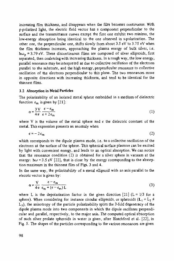
increasing film thickness, and disappears when the t'tim becomes continuous. With p-polarized light, the electric field vector has a component perpendicular to the surface and the transmittance curves except the first one exhibit two minima, the low~nergy absorption being identical to the one observed in s-polarization. The other one, the perpendicular one, shifts slowly from about 3.5 eV to 3.75 eV when the film thickness increases, approaching the plasma energy of bulk silver, i.e. hwp = 3.79 eV. These discontinuous films are composed of silver ellipsoids, first separated, then coalescing with increasing thickness. In a rough way, the low energy, parallel resonance may be interpreted as due to collective oscillation of the electrons parallel to the substrate, and the high energy, perpendicular resonance to collective oscillation of the electrons perpendicular to this plane. The two resonances move in opposite directions with increasing thickness, and tend to be identical for the thinnest films.
3.2 Absorption in Metal Particles
The polarizability of an isolated metal sphere embedded in a medium of dielectric function em is given by [21]:
3V e - e r a = (1)
4rr e + 2 e m
where V is the volume of the metal sphere and e the dielectric constant of the metal. This expression presents an anomaly when
e = - 2 era (2)
which corresponds to the dipole plasma mode, i.e. to a collective oscillation of the electrons at the surface of the sphere. This spherical surface plasmon can be excited by light with convenient energy, and leads to an optical absorption. We can notice that the resonance condition (2) is obtained for a silver sphere in vacuum at the energy: taco = 3.5 eV [22], that is close by the energy corresponding to the absorp- tion maximum in the thinnest film of Figs. 3 and 4.
In the same way, the polarizability of a metal ellipsoid with an axis parallel to the electric vector is given by:
V c - e m = - - ( 3 )
47r era + (e - era) L
where L is the depolarization factor in the given direction [21] (L = 1/3 for a sphere). When considering for instance circular ellipsoids, or spheroids (L1 = L2 L 3 ) , the anisotropy of the particle polarizability splits the 3-fold degeneracy of the dipole plasma mode into two components in which the dipole oscillates perpendi- cular and parallel, respectively, to the major axis. The computed optical absorption of such silver prolate spheroids in water is given, after Blatchford et al. [22], in Fig. 5. The shapes of the particles corresponding to the various resonances are given
98
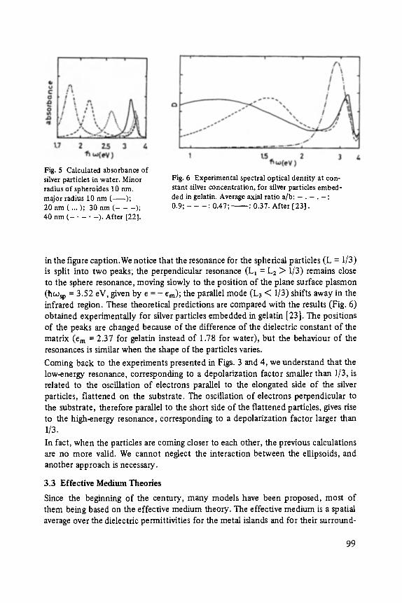
Fig. 5 Calculated absorbance of silver particles in water. Minor radius of spheroides 10 nm, major radius 10 nm ( - - ) ; 20 nm ( ... ); 30 nm (- - -); 40 nm ( . . . . . ). After [22].
Fig. 6 Experimental spectral optical density at con- stant silver concentration, for silver particles embed- ded in gelatin. Average axial ratio a/b: - . - . - : 0.9; - - - : 0.47; : 0.37. After [23].
in the figure caption.We notice that the resonance for the spherical particles (L = 1/3) is split into two peaks; the perpendicular resonance (L1 = L2 > 1/3) remains close to the sphere resonance, moving slowly to the position of the plane surface plasmon (hcoso = 3.52 eV, given by e = - era); the parallel mode (L3 < 1/3) shifts away in the infrared region. These theoretical predictions are compared with the results (Fig. 6) obtained experimentally for silver particles embedded in gelatin [23]. The positions of the peaks are changed because of the difference of the dielectric constant of the matrix (era = 2.37 for gelatin instead of 1.78 for water), but the behaviour of the resonances is similar when the shape of the particles varies.
Coming back to the experiments presented in Figs. 3 and 4, we understand that the low-energy resonance, corresponding to a depolarization factor smaller than 1/3, is related to the oscillation o f electrons parallel to the elongated side o f the silver particles, flattened on the substrate. The oscillation of electrons perpendicular to the substrate, therefore parallel to the short side of the flattened particles, gives rise to the high~nergy resonance, corresponding to a depolarization factor larger than 1/3. In fact, when the particles are coming closer to each other, the previous calculations are no more valid. We cannot neglect the interaction between the ellipsoids, and another approach is necessary.
3.3 Effective Medium Theories
Since the beginning of the century, many models have been proposed, most of them being based on the effective medium theory. The effective medium is a spatial average over the dielectric permittivities for the metal islands and for their surround-
99
ing medium, within the quasistatic approximation (the size of the particles being much smaller than the wavelength of the incident light, typically 10 nm or less), the interaction between the islands being neglected. As previously, the metal particles are assumed to be large enough for the macroscopic dielectric theory to be applicable (we will consider in Sect. 3.4 the case of very small particles where this approximation is no more valid).
Let us first consider the earliest Maxwell Garnett theory [15]. The metal particles are assumed to be spherical. One starts with Lorentz-Lorenz equation, expressing the relationship between the effective dielectric function we want to calculate, and the volume density n and the polarizability a of the dipoles (here the metal par- ticles) embedded in a medium characterized by the dielectric constant era:
~ - e r n 47rna ~ + 2e- - ' - -~ = 3 (4)
We can substitute for ,v the expression for the polarizability of an isolated metal sphere immersed in a medium e m (1). Eliminating t~ from Eqs. (1) and (4) leads to Maxwell Garnett 's result:
- - C m e - e m
e + 2 e m = f e + 2 e m (5)
where f is the fdling factor f = nV, i.e. the volume fraction of metal in the dis- continuous f'tim.
The extension of the theory to non-spherical particleshas been discussed by Galeener [24]: assuming the ellipsoids are identical in shape and orientation with a character- istic depolarization factor L, we substitute for t~ in Eq. (4) the expression for the polarizability of an isolated metallic ellipsoid immersed in a dielectric medium (Eq. (3)), and obtain:
= _ e - e m g - em 1 f . (6) e + 2 e m 3 e m + L ( e - e m )
Cohen et al. [25] have shown that this formula for ellipsoidal particles in a Lorentz spherical cavity leads to inconsistencies when L -~ 0 or 1, and have proposed that the cavity should be ellipsoidal instead. They obtained the equation:
- - e m e - - e m
= f (7) e m + L (e - era) e m + L (e - era)
which reduces to the Maxwell Gamet t result (Eq. (5)) in the case of metallic spheres (L = 1/3).
As the filling factor becomes smaller, the shape of the outer ellipsoid will more and more approach that of a sphere, and we can use, according to Polder et al. [26], Eq. (6) for a generalization to randomly oriented ellipsoids:
2 1 +~ f a ' = e ~ - - ( 8 )
t I00 1 - $ f a '
where a' is proportional to the averaged polarizability of the randomly oriented particles, given by:
3 1 e - 6 m
r = ~ ~ em + Li (e - era) (9) i=1
the summation being made over three principal axes of the ellipsoids, with L i being their depolarization factors.
From the arguments of Cohen et al. [25] it appears that Eqs. (8) and (9) are valid in the limit of small filling factors only. For randomly oriented ellipsoids the situation is not so clear and it is an open question whether the ellipsoidal cavities are more justified than the spherical ones also in this case. When the filling factor becomes large (typically f > 0.2 [27]), Bruggeman [28], followed by Polder et at. [26], gave a symmetrical expression for spheres, easily generalized to ellipsoids:
3 ( e - e e m - e ) E f F + L i ( e - e - ) + ( I - 0 g + L i ( e m - e -) =0. (10) i = l
In this model (called by some authors the "effective medium theory", as opposed to the Maxwell Gamett-type theories, although all of them are effective medium theories) the two components, metal and dielectric, are treated in equivalent manner, both of them being considered as embedded in an effective medium. Let us notice that this theory is a selfconsistent one and in principle is valid over the whole range of f. Indeed, this model predicts correctly the dielectric-metal transi- tion (sometimes called the optical percolation) observed in inhomogeneous media. However, as for the plasma resonances, theoretical calculations [29, 30] showed that Maxwell Garnett-type theories give better agreement with experimental results, while Bruggeman-type theories do not reproduce the adequate optical absorption, in the case of high concentration of silver, as it is observed experimentally. In con- tradistinction, all these theories give the same results for very low filling factors (f ~ 0). The discrepancies take place only for more important filling factors.
Recently, Ping Sheng [31 ] gave a symmetrical generalization of the Maxwell Garnett theory, which displays the dielectric anomaly and the percolation threshold. The results of his theory seem to be in good agreement with experimental data.
We have seen in section 3.2 that the observed plasma resonance is related to the pole of the expression of the polarizability given for an isolated ellipsoid (Eq. (3)). When considering an effective medium, which somewhat takes into account the far interaction between particles, the condition of plasma resonance should be changed. We said previously that only Maxwell Garnett-type theories give such a resonance for large filling factors. Therefore, we shall argue only about these models. Galeener's formula (Eq. (6)) gives the following resonance condition, defined by ~ ~ oo:
e = - e r n [ 3 3 _ f 1] (11)
I01
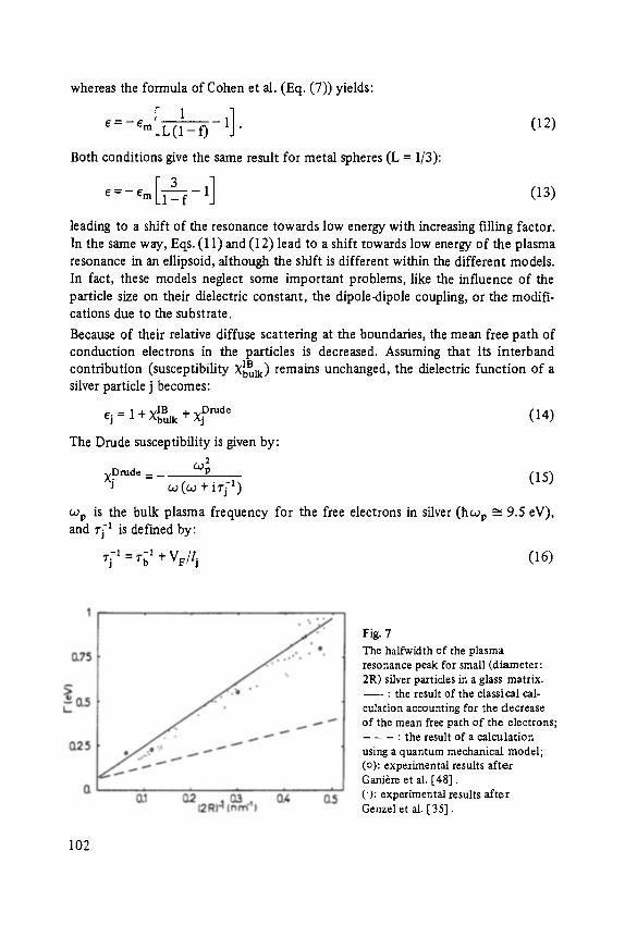
whereas the formula of Cohen et al. (Eq. (7)) yields:
1 1]. (12) e = - e m f L ( 1 - f )
Both conditions give the same result for metal spheres (L = 1/3):
leading to a shift of the resonance towards low energy with increasing filling factor. In the same way, Eqs. (11) and (12) lead to a shift towards low energy of the plasma resonance in an ellipsoid, although the shift is different within the different models. In fact, these models neglect some important problems, like the influence o f the particle size on their dielectric constant, the dipole-dipole coupling, or the modifi- cations due to the substrate.
Because of their relative diffuse scattering at the boundaries, the mean free path of conduction electrons in the particles is decreased. Assuming that its interband contribution (susceptibility IB Xbutk ) remains unchanged, the dielectric function of a silver particle j becomes:
= m + x~md. (14) ej I + XbuU,
The Drude susceptibility is given by: 2
xDrude _ COP co (co + i r ; 1) (15)
COp is the bulk plasma frequency for the free electrons in silver (hCOp - 9,5 eV), and r~ 1 is defined by:
rj -1 = rg 1 + VF//j (16)
Fig. 7 The halfwidth of the plasma resonance peak for small (diameter: 2R) silver particles in a glass matrix. - - : the result of the classical cal- culation accounting for the decrease of the mean free path of the electrons;
- - - : the result of a calculation using a quantum mechanical model; (o): experimental results after Gani6re et el. [48]. (9: experimental results after Genzel et el. [35].
102
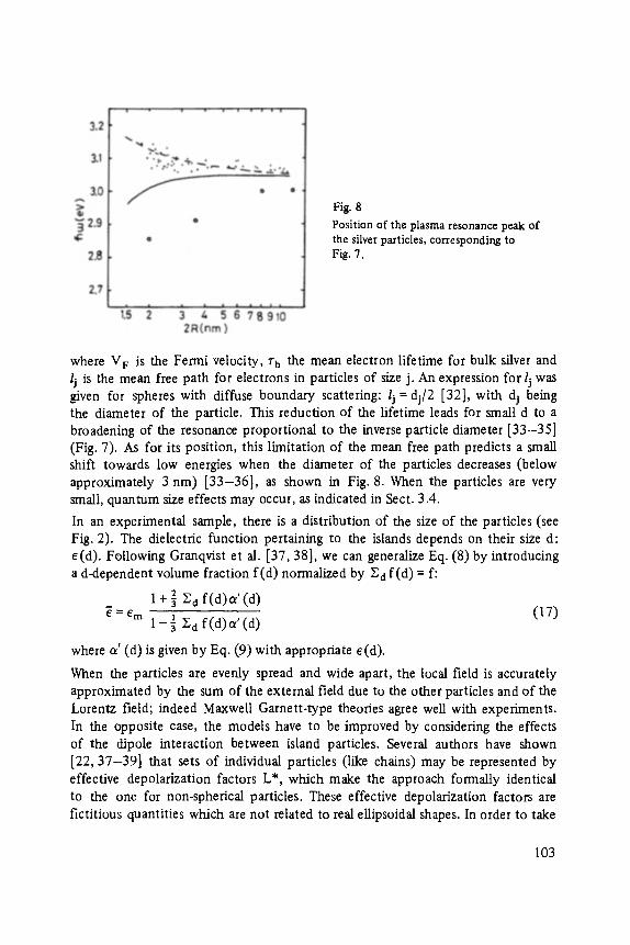
Fig. 8
Position of the plasma resonance peak of the silver particles, corresponding to Fig. 7.
where V v is the Fermi velocity, r b the mean electron lifetime for bulk silver and l i is the mean free path for electrons in particles of size j. An expression for lj was given for spheres with diffuse boundary scattering: lj = di/2 [32], with d i being the diameter of the particle. This reduction of the lifetime leads for small d to a broadening of the resonance proportional to the inverse particle diameter [33--35] (Fig. 7). As for its position, this limitation of the mean free path predicts a small shift towards low energies when the diameter of the particles decreases (below approximately 3 nm) [33-36], as shown in Fig. 8. When the particles are very smalI, quantum size effects may occur, as indicated in Sect. 3.4.
In an experimental sample, there is a distribution of the size of the particles (see Fig. 2). The dielectric function pertaining to the islands depends on their size d: e(d). Following Granqvist et al. [37, 38], we can generalize Eq. (8) by introducing a d-dependent volume fraction f(d) normalized by Y. d f(d) = f:
1 + ~ ~d f (d)a ' (d )
1 - ~ F- d f (d)c((d) (17)
where a' (d) is given by Eq. (9) with appropriate e (d).
When the particles are evenly spread and wide apart, the local field is accurately approximated by the sum of the external field due to the other particles and of the Lorentz field; indeed Maxwell Garnett-type theories agree well with experiments. In the opposite case, the models have to be improved by considering the effects of the dipole interaction between island particles. Several authors have shown [22, 37-39] that sets of individual particles (like chains) may be represented by effective depolarization factors L*, which make the approach formally identical to the one for non-spherical particles. These effective depolarization factors are fictitious quantities which are not related to real ellipsoidal shapes. In order to take
103

into account the local-field effects, Bedeaux and Vlieger [40] made in Eq. (8) the substitution:
f a ' f c t ' ~ - - (18)
t 4(A)
where t is the average mass thickness of the film, and (A) is an "effective distance" roughly equal to the distance between the centers of adjacent islands. This sub- stitution is equivalent to the introduction of "effective depolarization factors": L~ = L i - t f / 4 ( A ) in Eq. (9). This treatment was successfully applied to discontin- uous gold frims [38, 41]. Thus, the effect of the interaction between metal grains is a decrease of the polarization factors, giving rise to a shift of the plasma resonan- ces towards lower energies with increasing coupling strength.
Finally, the influence of the substrate on the resonances is not negligible. It is usually treated in the dipole approximation, in which only the dipole-dipole inter- action between the particle and its image is taken into account [7, 8]. Other treat- ments have been used [42], but all o f them lead qualitatively to similar results, namely, to a shift towards lower energies with respect to the case where the influence of the substrate is ignored. Yoshida et al. [6] have shown that for discontinuous films on a substrate, the choice of the right dielectric constant e m for the inter- island medium is not obvious. If the particles are considered to be placed in air or in vacuum, e m is equal to unity. However, the contribution from the dielectric con- stant of the substrate e s to e m should be taken into account. David [16] and Doremus [33], for example, adopted e m = ( 1 + es)/2 and e m = es, respectively, while for Yoshida and coworkers, the right ena to be considered is dependent on the film thickness.
From the preceding discussion, it can be concluded that if a Maxwell Garnett- type theory may be correctly used to describe the optical properties of discontinuous films, many corrections, which depend on the nature of the films, have to be added. Electron micrographs are of great importance to determine the size distribution of particles, which leads to a broadening of the resonance. The modification of the mean free path of the conduction electrons, dependent on the size of the particles, must not be forgotten. The dipole-dipole interactions between the islands, or via the substrate,with the image-dipole, have a large influence on the optical properties, too: it leads, practically, to a modification of the depolarization factors and their substitution by effective depolarization factors, which have to be determined for each experimental situation.
It seems impossible to give a general method to determine a priori the optical properties of a discontinuous film, and each particular system has to be investigated in an exhaustive way, in order to choose the description appropriate to explain the observed properties.
104
3.4 Extremely Thin Films
When the amount of silver atoms deposited on a substrate is very low (mass thick- ness below 0.1 nm), and the number of nucleation sites is large enough, very small silver spheres (diameters of a few nm) grow at the surface of the substrate. In fact, the optical properties of very small silver particles have been studied especially when embedded in a matrix: photosensitive glasses [46], silver diffusion in glass matrix [36] or silver condensation in rare gas matrix at low temperature [47], and there are only very few optical measurements for silver particles on a substrate [13,45].
The spheres are here isolated, therefore the effective medium theories need not be applied. Eq. (1) should lead to a resonance occurring at the frequency for which e(~o) + 2era = 0. However, some experimental works [36,48] showed a shift of this plasma resonance peak to lower energies (red shift), for spherical particles with a diameter less than 5 nm. Classical calculations (i.e. the decrease of the mean free path discussed before), leading only to a much smaller red shift when the diameter is below 3 nm, are not sufficient to explain the observed effect (Fig. 8), although the width of the plasma resonance is well predicted (Fig. 7).
In fact, for so small particles, a new effect comes into play: due to size quantization, the conduction band breaks up into discrete levels [49]. This effect, called the quantum size effect, has been studied theoretically by several authors [35, 50-52], but the use of a quantum mechanical model for the dielectric constant predicts a blue shift of the resonance, as shown in Fig. 8 [48]. This is contrary to most experi- mental results, which rather show a red shift as previously mentioned. However, in more recent experiments a blue shift was indeed observed: in Genzel et al. experi- ments [35], reproduced in Figs. 7 and 8, the shift is almost of the same order as the spread in experimental data; in Abe et al. results [47] the shift is as large as 0.4 eV for spheres with diameters below 2 nm, and is very well reproduced by the calcula- tions of Ekardt et al. [53]. Some preliminary results we obtained for silver spheres grown on alumina showed a blue shift as well.
The shift of the resonance to lower energies has been tentatively explained by several different considerations: (a) by the fact that the surface of the particles is not sharp but exhibits a smooth transition from the embedding medium to the bulk [54]; (b) by the nonlocal response of the small metal particles [55]. The question of the red or blue shift of the plasma resonance is not yet totally under- stood, and the position of the peaks is still controversial.
Several theoretical approaches have been proposed recently for a better understand- ing of the optical properties of these very small particles [56-58] and this interesting problem remains under intense investigation.
105
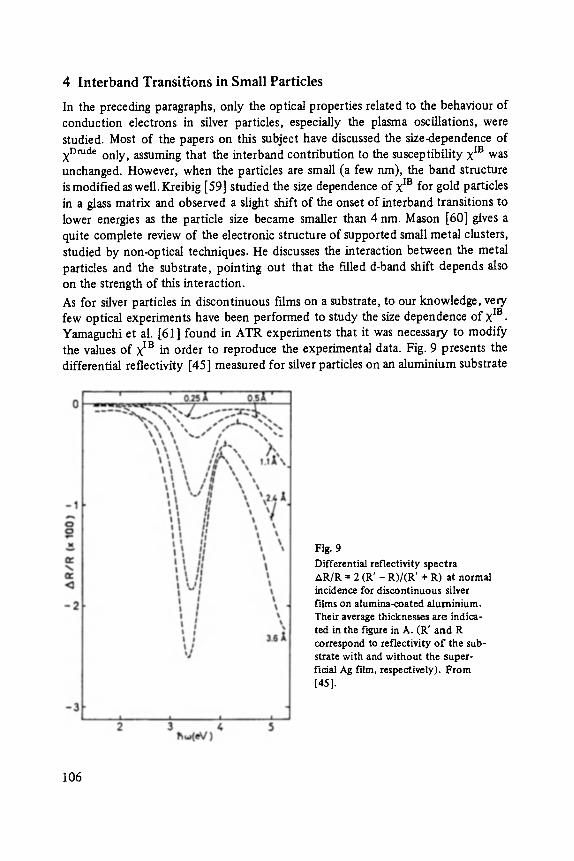
4 I n t e r b a n d T r a n s i t i o n s in Small Par t i c l e s
In the preceding paragraphs, only the optical properties related to the behaviour of conduction electrons in silver particles, especially the plasma oscillations, were studied. Most of the papers on this subject have discussed the size-dependence of X Drude only, assuming that the interband contribution to the susceptibility X m was unchanged. However, when the particles are small (a few nm), the band structure is modified as well. Kreibig [59] studied the size dependence of X Ia for gold particles in a glass matrix and observed a slight shift of the onset of interband transitions to lower energies as the particle size became smaller than 4 nm. Mason [60] gives a quite complete review of the electronic structure of supported small metal clusters, studied by non-optical techniques. He discusses the interaction between the metal particles and the substrate, pointing out that the fdled d-band shift depends also on the strength of this interaction.
As for silver particles in discontinuous films on a substrate, to our knowledge, very few optical experiments have been performed to study the size dependence o f x IB. Yamaguchi et al. [61] found in ATR experiments that it was necessary to modify the values of X IB in order to reproduce the experimental data. Fig. 9 presents the differential reflectivity [45] measured for silver particles on an aluminium substrate
Fig. 9 Differential reflectivity spectra AR/R = 2 (R' - R)/(R' + R) at normal incidence for discontinuous silver films on alumina-coated alurninium. Their average thicknesses are indica- ted in the figure in A. (R' and R correspond to reflectivity of the sub- strate with and without the super- tidal Ag fdm, respectively). From [45].
106
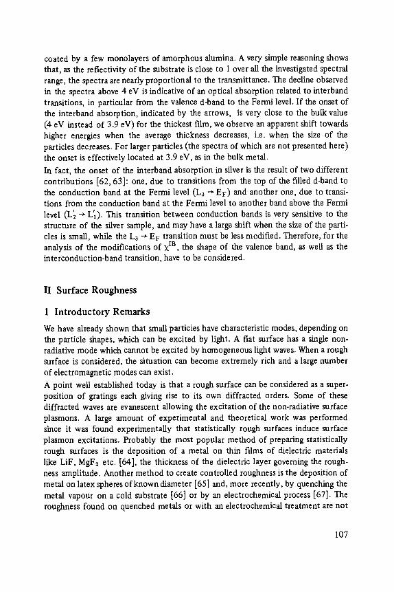
coated by a few monolayers of amorphous alumina. A very simple reasoning shows that, as the reflectivity of the substrate is close to 1 over all the investigated spectral range, the spectra are nearly proportional to the transmittance. The decline observed in the spectra above 4 eV is indicative of an optical absorption related to interband transitions, in particular from the valence d-band to the Fermi level. If the onset of the interband absorption, indicated by the arrows, is very close to the bulk value (4 eV instead of 3.9 eV) for the thickest t~flm, we observe an apparent shift towards higher energies when the average thickness decreases, i.e. when the size of the particles decreases. For larger particles (the spectra of which are not presented here) the onset is effectively located at 3.9 eV, as in the bulk metal.
In fact, the onset of the interband absorption in silver is the result of two different contributions [62, 63]: one, due to transitions from the top of the filled d-band to the conduction band at the Fermi level (L3 ~ EF) and another one, due to transi- tions from the conduction band at the Fermi level to another band above the Fermi level (L~ ~ L'I). This transition between conduction bands is very sensitive to the structure of the silver sample, and may have a large shift when the size of the parti- cles is small, while the L3 ~ EF transition must be less modified. Therefore, for the analysis of the modifications of X m, the shape of the valence band, as well as the interconduction-band transition, have to be considered.
I I Surface Roughness
1 Introductory R e m a r k s
We have already shown that small particles have characteristic modes, depending on the particle shapes, which can be excited by light. A fiat surface has a single non- radiative mode which cannot be excited by homogeneous light waves. When a rough surface is considered, the situation can become extremely rich and a large number of electromagnetic modes can exist.
A point well established today is that a rough surface can be considered as a super- position of gratings each giving rise to its own diffracted orders. Some of these diffracted waves are evanescent allowing the excitation of the non-radiative surface plasmons. A large amount of experimental and theoretical work was performed since it was found experimentally that statistically rough surfaces induce surface plasmon excitations. Probably the most popular method of preparing statistically rough surfaces is the deposition of a metal on thin films of dielectric materials like LiF, MgF2 etc. [64], the thickness of the dielectric layer governing the rough- ness amplitude. Another method to create controlled roughness is the deposition of metal on latex spheres of known diameter [65] and, more recently, by quenching the metal vapour on a cold substrate [66] or by an electrochemical process [67]. The roughness found on quenched metals or with an electrochemical treatment are not
107

well characterized till now although their knowledge is crucial for understanding surface enhanced Raman scattering (SERS). Both types of surfaces were recognized as having, in the case of silver, abnormal optical absorptions [68] which are clearly not due to plane surface plasmons as is usually understood. Some aspects of this problem will be discussed in the next paragraph in the case of quenched silver f'rims.
2 Small Roughness
It is now clear that any surface displaying a SERS effect is rough on a macroscopic scale. Nevertheless, a question which is still completely open concerns the micro- scopic roughness of such surfaces. In contradistinction with large roughness, extremely small roughness was studied only in few cases although in most cases atomic rough- ness gives rise to measurable optical signals with the to-day available technique. It should also be possible to investigate the electronic structure related to surface defects and crystal growth processes. Concerning this point one should mention the work of Gauch and Quentel [69] who studied by ellipsometry the (0001) face of cadmium during growth, evaporation and equilibrium of the crystal. In the two first cases, oscillations with time of the ellipsometric parameters were found by Gauch and Quentel and were interpreted as being due to a periodic modification of the surface by the growth of the steps generated by screw dislocations or due to two-dimensional nucleation for each monolayer. Very small roughness was also investigated by L6pez-Rios et al. [70] measuring the change in reflecfivity induced by silver deposits of different thicknesses on a clean silver surface kept at 140 K in ultra-high vacuum. Fig. 10 shows experimental results obtained with a silver deposit 1.9 nm thick [70]. The normal incidence differential reflectivity' AR/R = 2 (R - R')/(R + R') (R' and R being the reflectivities of the bare surface and of the surface covered with the quenched deposit, respectively) is shown for different temperatures during annealing from 140 K to room temperature. The important peaks at 4 eV are indicative of the low reflectivity of Ag at this frequency and of the finite thickness of the silver substrate. The minimum at about 3.5 eV is due to the surface roughness and corresponds to the frequency of surface plasmons for a nearly flat surface. We notice that this structure disappears with increasing temper- ature. Fig. 11 shows the results of a calculation [70] corresponding to the experi- ments of Fig. 10 using the approximations of Kretschmann and Kr6ger [71]. The calculation was performed for a model which assumes that the surface roughness can be described by a Gaussian correlation function with a correlation length a = 50 nm and different values of the root mean square roughness S. I t must be underlined that the values of AR/R in Fig. 10 are in the 10 -2 range. This example shows that optical techniques have enough sensitivity to investigate very small atomic roughness. Differential reflectivity was also used to investigate the intensity of electromagnetic fields at rough silver surfaces [45].
108
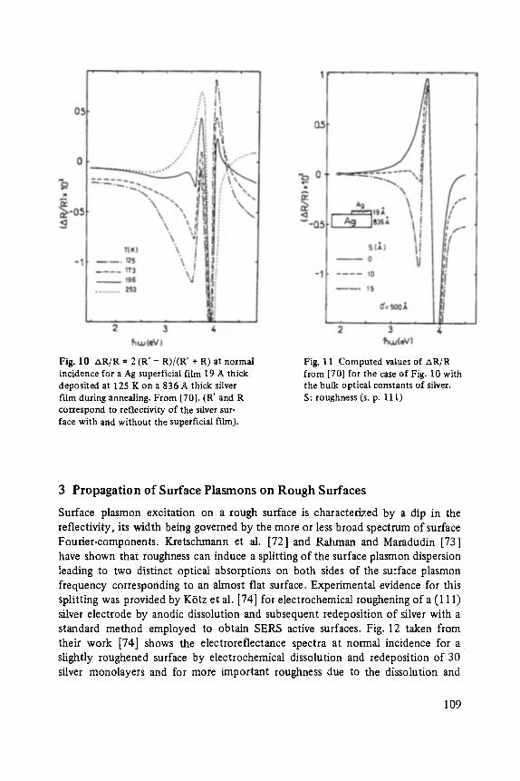
Fig. 10 AR/R = 2 (R' - R)/(R' + R) at normal incidence for a Ag superficial film 19 A thick deposited at 125 K on a 836 A thick silver film during annealing. From [701. (R' and R correspond to reflectivity of the silver sur- face with and without the superficial film).
Fig. 11 Computed values of AR/R from [70] for the case of Fig. 10 with the bulk optical constants of silver. S: roughness (s. p. 111)
3 Propagation of Surface Plasmons on Rough S u r f a c e s
Surface plasmon excitation on a rough surface is characterized by a dip in the reflectivity, its width being governed by the more or less broad spectrum of surface Fourier-components. Kretschmann et al. [72] and Rahman and Maradudin [73] have shown that roughness can induce a splitting of the surface plasmon dispersion leading to two distinct optical absorptions on both sides of the surface plasmon frequency corresponding to an almost flat surface. Experimental evidence for this splitting was provided by KStz et al. [74] for electrochemical roughening of a (111) silver electrode by anodic dissolution and subsequent redeposition of silver with a standard method employed to obtain SELLS active surfaces. Fig. 12 taken from their work [74] shows the electroreflectance spectra at normal incidence for a slightly roughened surface by electrochemical dissolution and redeposition of 30 silver monolayers and for more important roughness due to the dissolution and
109
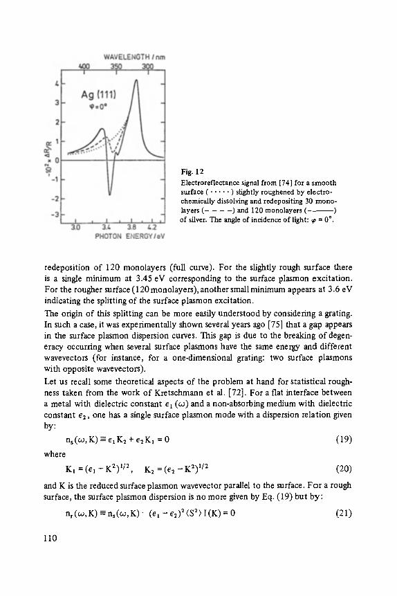
Fig. 12 Electroreflectance signal from [74] for a smooth surface ( . . . . . ) slightly roughened by electro- chemically dissolving and redepositing 30 mono- layers ( . . . . ) and 120 monolayers ( ) of silver. The angle of incidence of light: 9 = 0 ~
redeposition of 120 monolayers (full curve). For the slightly rough surface there is a single minimum at 3.45 eV corresponding to the surface plasmon excitation. For the rougher surface (120 monolayers), another small minimum appears at 3.6 eV indicating the splitting of the surface plasmon excitation.
The origin of this splitting can be more easily understood by considering a grating. In such a case, it was experimentally shown several years ago [75] that a gap appears in the surface plasmon dispersion curves. This gap is due to the breaking of degen- eracy occurring when several surface plasmons have the same energy and different wavevectors (for instance, for a one-dimensional grating: two surface plasmons with opposite wavevectors).
Let us recall some theoretical aspects of the problem at hand for statistical rough- ness taken from the work of Kretschmann et al. [72]. For a flat interface between a metal with dielectric constant el (co) and a non-absorbing medium with dielectric constant e2, one has a single surface plasmon mode with a dispersion relation given by:
ns(co, K) = e l K 2 + e2Kl = 0 (19)
where
K1 = (el - K2) 1/2 , K2 = (e2 - K2) 1/2 (20)
and K is the reduced surface plasmon wavevector parallel to the surface. For a rough surface, the surface plasmon dispersion is no more given by Eq. (19) but by :
nr (~o, K ) = ns(w,K ) - (el - e2) 2 (S 2) I (K) = 0 (21)
110
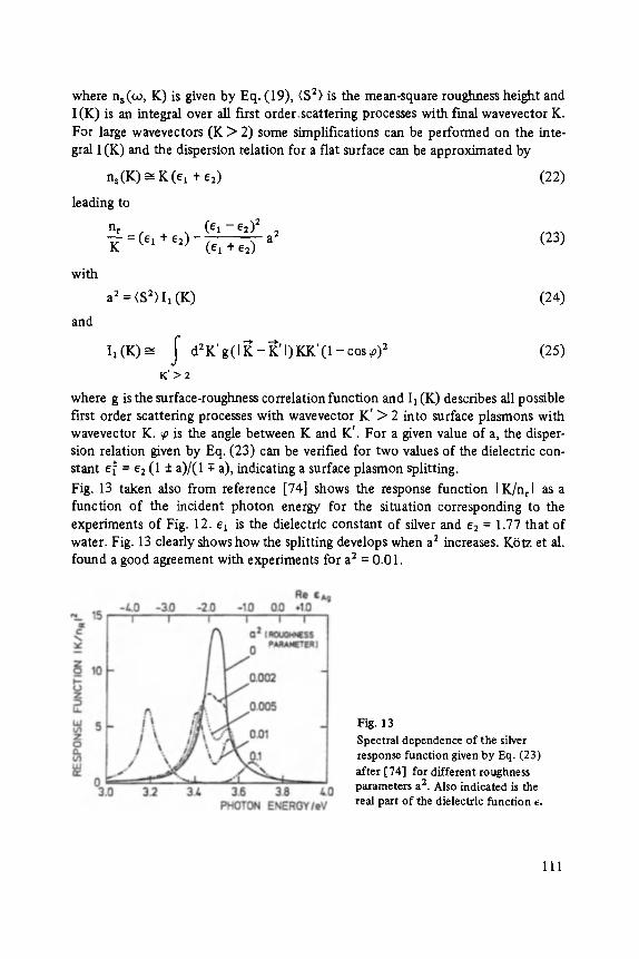
where ns(r K) is given by Eq. (19), (S = ) is the mean-square roughness height and I (K) is an integral over all ftrst order.scattering processes with final wavevector K. For large wavevectors (K > 2) some simplifications can be performed on the inte- gral I (K) and the dispersion relation for a fiat surface can be approximated by
ns(K) ~ K(e l + e=)
leading to
n r (el - e=) 2 = (el + e=) (el + e=)
with
and
(22)
a 2 (23)
a = = (S 2) I1 (K) (24)
Ia(K)--- f d 2 K ' g ( I K - K ' l ) K K ' ( 1 - c o s ~ 0 ) = (25)
K'> 2
where g is the surface-roughness correlation function and I1 (K) describes all possible first order scattering processes with wavevector K' > 2 into surface plasmons with wavevector K. ~0 is the angle between K and K'. For a given value of a, the disper- sion relation given by Eq. (23) can be verified for two values of the dielectric con- stant e~ = e2 (1 + a)/(1 z~ a), indicating a surface plasmon splitting.
Fig. 13 taken also from reference [74] shows the response function I K/nr as a function of the incident photon energy for the situation corresponding to the experiments of Fig. 12. el is the dielectric constant of silver and e2 = 1.77 that of water. Fig. 13 clearly shows how the splitting develops when a 2 increases. K6tz et al. found a good agreement with experiments for a 2 = 0.01.
Fig. 13 Spectral dependence of the silver response function given by Eq. (23) after [74] for different roughness parameters a 2. Also indicated is the real part of the dielectric function e.
iii
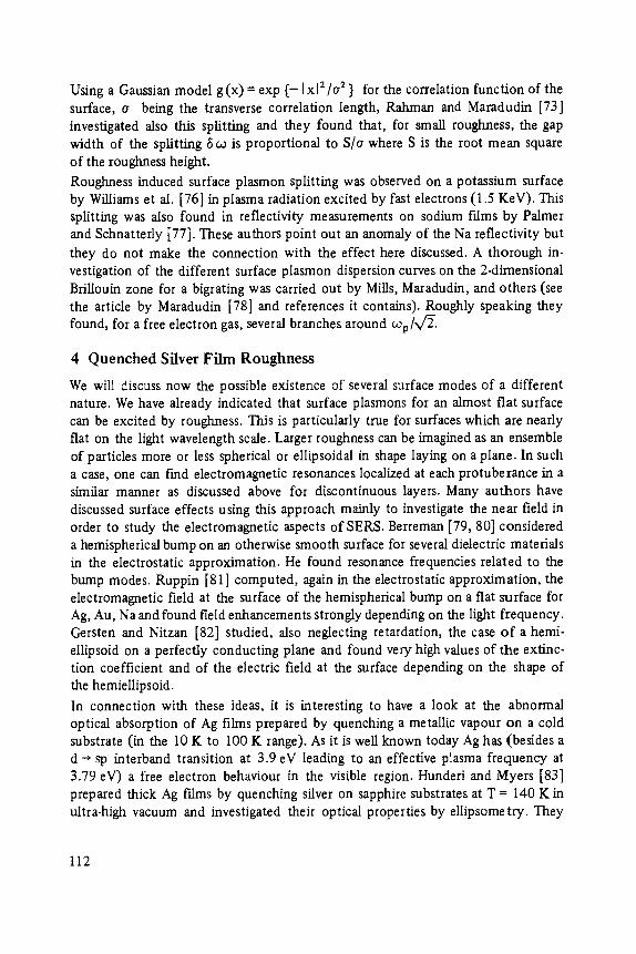
Using a Gaussian model g (x) = exp {- Ix l 2/o 2 } for the correlation function of the surface, o being the transverse correlation length, Rahman and Maradudin [73] investigated also this splitting and they found that, for small roughness, the gap width of the splitting ~ 6o is proportional to S/a where S is the root mean square of the roughness height.
Roughness induced surface plasmon splitting was observed on a potassium surface by Williams et al. [76] in plasma radiation excited by fast electrons (1.5 KeV). This splitting was also found in reflectivity measurements on sodium films by Palmer and Schnatterly [77]. These authors point out an anomaly of the Na refiectivity but they do not make the connection with the effect here discussed. A thorough in- vestigation of the different surface plasmon dispersion curves on the 2-dimensional Brillouin zone for a bigrating was carried out by Mills, Maradudin, and others (see the article by Maradudin [78] and references it contains). Roughly speaking they found, for a free electron gas, several branches around cop/x,~2.
4 Quenched Silver Fi lm Roughness
We will discuss now the possible existence of several surface modes of a different nature. We have already indicated that surface plasmons for an almost flat surface can be excited by roughness. This is particularly true for surfaces which are nearly flat on the light wavelength scale. Larger roughness can be imagined as an ensemble of particles more or less spherical or ellipsoidal in shape laying on a plane. In such a case, one can fred electromagnetic resonances localized at each protuberance in a similar manner as discussed above for discontinuous layers. Many authors have discussed surface effects using this approach mainly to investigate the near field in order to study the electromagnetic aspects ofSERS. Berreman [79, 80] considered a hemispherical bump on an otherwise smooth surface for several dielectric materials in the electrostatic approximation. He found resonance frequencies related to the bump modes. Ruppin [81] computed, again in the electrostatic approximation, the electromagnetic field at the surface of the hemispherical bump on a flat surface for Ag, Au, Na and found field enhancements strongly depending on the light frequency. Gersten and Nitzan [82] studied, also neglecting retardation, the case of a hemi- ellipsoid on a perfectly conducting plane and found very high values of the extinc- tion coefficient and of the electric field at the surface depending on the shape of the hemiellipsoid.
In connection with these ideas, it is interesting to have a look at the abnormal optical absorption of Ag films prepared by quenching a metallic vapour on a cold substrate (in the 10 K to 100 K range). As it is well known today Ag has (besides a d -* sp interband transition at 3.9 eV leading to an effective plasma frequency at 3.79 eV) a free electron behaviour in the visible region. Hunderi and Myers [83] prepared thick Ag films by quenching silver on sapphire substrates at T = 140 K in ultra-high vacuum and investigated their optical properties by ellipsometry. They
112
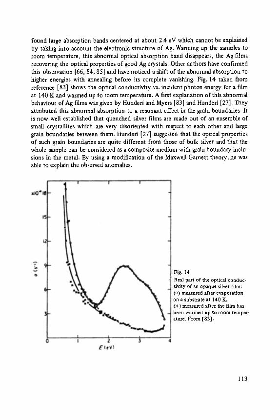
found large absorption bands centered at about 2.4 eV which cannot be explained by taking into account the electronic structure of Ag. Warming up the samples to room temperature, this abnormal optical absorption band disappears, the Ag Frims recovering the optical properties of good Ag crystals. Other authors have confirmed this observation [66, 84, 85] and have noticed a shift of the abnormal absorption to higher energies with annealing before its complete vanishing. Fig. 14 taken from reference [83] shows the optical conductivity vs. incident photon energy for a film at 140 K and warmed up to room temperature. A first explanation of this abnormal behaviour of Ag films was given by Hunderi and Myers [83] and Hunderi [27]. They attributed this abnormal absorption to a resonant effect in the grain boundaries. It is now well established that quenched silver films are made out of an ensemble of small crystallites which are very disoriented with respect to each other and large grain boundaries between them. Hunderi [27] suggested that the optical properties of such grain boundaries are quite different from those of bulk silver and that the whole sample can be considered as a composite medium with grain boundary inclu- sions in the metal. By using a modification of the Maxwell Garnett theory, he was able to explain the observed anomalies.
Fig. 14 Real part of the optical conduc- tivity of an opaque silver film: (o) measured after evaporation on a substrate at 140 K, (• measured after the firm has been warmed up to room temper- atttre. From [83].
113
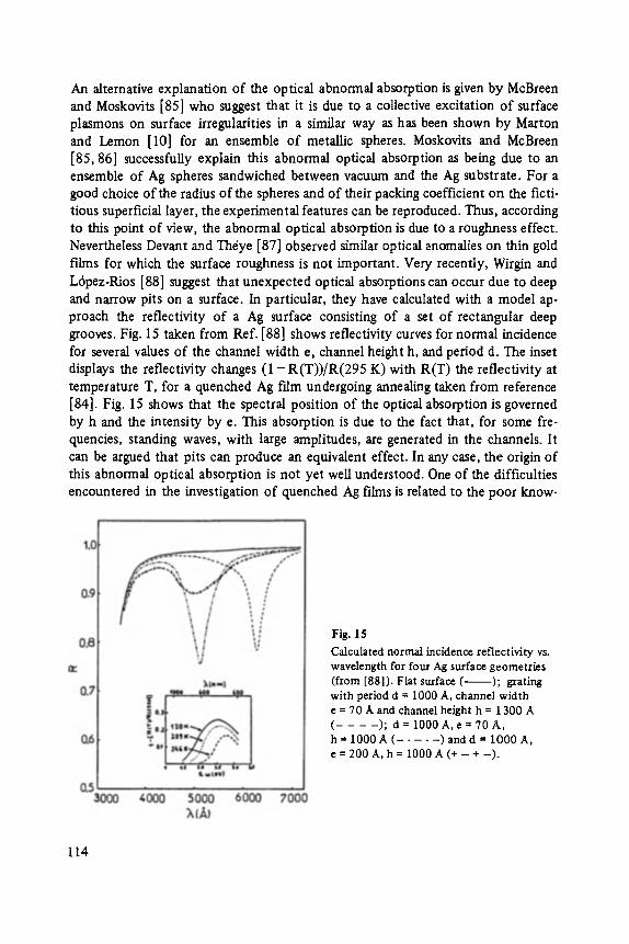
An alternative explanation of the optical abnormal absorption is given by McBreen and Moskovits [85] who suggest that it is due to a collective excitation of surface plasmons on surface irregularities in a similar way as has been shown by Marton and Lemon [10] for an ensemble of metallic spheres. Moskovits and McBreen [85, 86] successfully explain this abnormal optical absorption as being due to an ensemble of Ag spheres sandwiched between vacuum and the Ag substrate. For a good choice of the radius of the spheres and of their packing coefficient on the ficti- tious superficial layer, the experimental features can be reproduced. Thus, according to this point of view, the abnormal optical absorption is due to a roughness effect. Nevertheless Devant and Th~ye [87] observed similar optical anomalies on thin gold films for which the surface roughness is not important. Very recently, Wirgin and L6pez-Rios [88] suggest that unexpected optical absorptions can occur due to deep and narrow pits on a surface. In particular, they have calculated with a model ap- proach the reflectivity of a Ag surface consisting of a set of rectangular deep grooves. Fig. 15 taken from Ref. [88] shows reflectivity curves for normal incidence for several values of the channel width e, channel height h, and period d. The inset displays the reflectivity changes (1 - R(T))/R(295 K) with R(T) the reflectivity at temperature T, for a quenched Ag film undergoing annealing taken from reference [84]. Fig. 15 shows that the spectral position of the optical absorption is governed by h and the intensity by e. This absorption is due to the fact that, for some fre- quencies, standing waves, with large amplitudes, are generated in the channels. It can be argued that pits can produce an equivalent effect. In any case, the origin of this abnormal optical absorption is not yet well understood. One of the difficulties encountered in the investigation of quenched Ag films is related to the poor know-
Fig. 15 Calculated normal incidence reflectivity vs. wavelength for four Ag surface geometries (from [881). Flat surface ( ); grating with period d = 1000 A, channel width e = 70 k and channel height h = 1300 A ( .... ); d=1000k, e=70A,
h = I000 A ( ..... ) and d = I000 A,
e = 200 A,h = I000 A (+ - + -).
114
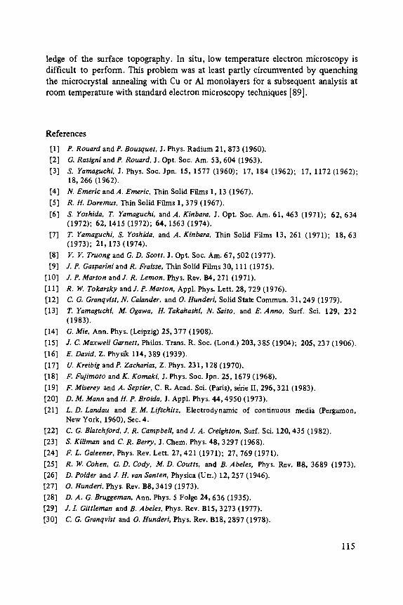
ledge of the surface topography. In situ, low temperature electron microscopy is difficult to perform. This problem was at least partly circumvented by quenching the microcrystal annealing with Cu or A1 monolayers for a subsequent analysis at room temperature with standard electron microscopy techniques [89].
References
[1] P. Rouard andP. Bousquet, J. Phys. Radium 21,873 (1960). [2] G. Rasigni and P. Rouard, J. Opt. Soc. Am. 53,604 (1963). [3] S. YarnaguchL J. Phys. Soc. Jpn. 15, 1577 (1960); 17, 184 (1962); 17, 1172 (1962);
18, 266 (1962). [4] N. Emetic andA. Emeric, Thin Solid Films 1, 13 (1967). [5] R.H. Doremus, Thin Solid Films 1,379 (1967).
[6] S. Yoshida, T. Yamaguchh and A. Kinbara, J. Opt. Soc. Am. 61,463 (1971); 62, 634 (1972); 62, 1415 (1972); 64, 1563 (I974).
[7] T. YamaguchL S. Yoshida, and A. Kinbara, Thin Solid Films 13, 261 (1971); 18, 63 (1973); 21,173 (1974).
[8] V. V. Truong and G. D. Scott, J. Opt. Soc. Am. 67, 502 (1977). [9] s P. Gasparini and R. Fraisse, Thin Solid Films 30, 111 (1975).
[10] J.P. MartonandJ. R. Lemon, Phys. Rev. B4,271(1971).
[11] R.W. Tokarsky and d. P. Marton, Appl. Phys. Lett. 28, 729 (1976). [12] C.G. Granqvist, N. Calander, and O. Hunderi, Solid State Commun. 31,249 (1979). [13] T. Yamaguchi, M. Ogawa, H. Takahashi, N. Saito, and E. Anno, Surf. Sci. 129, 232
(1983). [14] G. Mie, Ann. Phys. (Leipzig) 25, 377 (1908). [15] J.C. Maxwell Garnett, Philos. Trans. R. Soc. (Lond.) 203, 385 (1904); 205, 237 (1906). [16] E. David, Z. Physik 114, 389 (1939). [17] U. Kreibig andP. Zacharias, Z. Phys. 231,128 (1970). [18] F. Fu/imoto and K. Komaki, J. Phys. Soc. Jpn. 25, 1679 (1968). [19] F. Miserey and A. Septier, C. R. Acad. Sci. (Paris), s&ie II, 296,321 (1983). [20] D.M. Mann and H. P. Broida, J. Appl. Phys. 44, 4950 (1973). [21] L.D. Landau and E. M. Lifschitz, Electrodynamie of continuous media (Pergamon,
New York, 1960), See. 4. [22] C. G. Blatchford, J. R. Campbell, and s A. Creighton, Surf. Sci. 120, 435 (1982). [23] S. Killman and C. R. Berry, J. Chem. Phys. 48, 3297 (1968). [24] F.L. Galeener, Phys. Rev. Lett. 27,421 (1971); 27,769 (1971). [25] R. Ir Cohen, G. D. Cody, M. D. Courts, and B. Abeles, Phys. Rev. BS, 3689 (1973). [26] 19. Polder and J. H. van Santen, Physica (Utr.) 12, 257 (1946). [27] O. Hunderi, Phys. Rev. B8, 3419 (1973). [28] D.A.G. Bruggeman, Ann. Phys. 5 Folge 24,636 (1935). [29] J. L Gittleman and B. Abeles, Phys. Rev. BI5, 3273 (1977). [30] C.G. Granqvist and O. Hunderi, Phys. Rev. B18, 2897 (1978).
115
[31] Ping Sheng, Phys. Rev. Lett. 45, 60 (1980). [32] Ir T. Doyle, Phys. Rev. 111, 1067 (1958). [33] P.H. Doremus, J. Chem. Phys. 42,414 (1965). [34] U. Kreibig and C. V. Fragstein, Z. Phys. 224, 307 (1969). [35] L. Genzel, T. P. Martin, and U. Kreibig, Z. Phys. B21,339 (1975). [36] M.A. Smithardt, Solid State Commun. 13, 153 (1973). [37] C.G. Granqvist and O. Hunderi, Phys. Rev. B16, 3513 (1977). [38] S. Norrman, T. Andersson, and C. G. Granqvist, Phys. Rev. B18, 674 (1978).
[39] A. Meesen, J. Physique 33,371 (1972). [40] D. Bedeaux andJ. Vlieger, Physica (Utr.) 73, 287 (1974).
[41] D.N. Jarret and L. Ward, J. Phys. D9, 1515 (1976).
[42] R. Ruppin, Surf. Sci. 127,108 (1983). [43] J .A. Venables, Thin Solid Films 32, 135 (1976). [44] H. Schmeisser, Thin Solid Films 22, 83 (1974). [45] Y. Borensztein, T. L6pez-Rios, and G. Vuye, J. Physique 12, C10-475 (1983).
[46] L. Genzel and U. Kreibig, Z. Phys. B37, 93 (1980). [47] H. Abe, IV. Schultze, and B. Tesche, Chem. Phys. 47, 95 (1980). [48] J. D. Gani~re, R. Rechsteiner, and M. A. Smithardt, Solid State Commun. 16, 113
(1975).
[49] R. Kubo, J. Phys. Soc. Jpn. 17,975 (1962).
[50] A. Kawabata and R. Kubo, J. Phys. Soc. Jpn. 21, 1765 (1966).
[51] M. Cini and P. Ascarelli, J. Phys. F4, 1998 (1974).
[52] A. A. Luschnikov and A. J. Simonov, Z. Phys. 270, 17 (1974).
[53] 14/. Ekardt, D. B. Tran Thoai, F. Frank, and W. Schulze, Solid State Commun. 46, 571 (1983).
[54] P. Ascarelli and M. Cini, Solid State Commun. 18, 385 (1976). [55] P. Apell and A. Ljungbert, Solid State Commun. 44, 1367 (1982). [56] D.M. Wood and N. W. Ashcro[t, Phys. Rev. B25, 6255 (1982). [57] A. Ljungbert and P. Apell, Solid State Commun. 46, 47 (1983). [58] P. Ahlqvist, P. de Andrds, R. Monreal, and F. Flores, J. Physique 12, C10-375 (1983). [59] U. Kreibig, J. Physique 38, C2-97 (1977). [60] M.G. Mason, Phys. Rev. B27, 748 (1983). [61] T. Yamaguchi, M. Ogawa, H. Takahashi, and N. Saito, Surf. Sci. 129, 232 (1983). [62] B.F. Schmidt and D. W. Lynch, Phys. Rev. B3, 4015 (1971). [63] P. Winsemius, Thesis Leiden University (1973). [64] H. Raether in "Surface Polaritons": Modem problems in condensed matter sciences,
ed. V. M. Agranovitch andA. A. Maradudin, North-Holland, 1982, p. 331. [65] S. O. Sari, D. K. Cohen, and K. D. Scherkoske, Phys. Rev. B21, 2162 (1980). [66] T. L6pez-Rios, Y. Borensztein, and G. Vuye, J. Physique Lettres 44, L99 (1983).
[67] M. Fleischmann, P. J. Hendra, andA. G. McQuillan, Chem. Phys. Lett. 26,123 (1974). [68] A. Otto, to be published in "Light Scattering in Solids", Vol. IV, ed. M. Cardona and
G. Gitntherodt, Springer Verlag. [69] M. Gauch and G. Quentel, Surf. Sci. 108,617 (1981).
116
[70] T. L6pez.Rios, Y. Borensztein, and G. Vuye, to be published in Phys. Rev. B.
[71] E. Kretschmann and E. Kr6ger, J. Opt. Soc. Am. 65,150 (1975).
[72] E. Kretschmann, T. L. Ferell, and J.. C. Ashley, Phys. Rev. Lett. 42, 1312 (1979).
[73] T.S. Rahman, A. A. Maradudin, Phys. Rev. B21, 2137 (1980).
[74] R. K6tz, M. J. Lewerenz, and E. Kretschmann, Phys. Lett. 70A, 452 (1979).
[75] R. H. Ritchie, E. T. Arakawa, J. J. Cowan, and R. N. Hamm, Phys. Rev. Lett. 21, 1530 (1968).
[76] N. IV. Williams, J. C. Ashley, E. Kretschmann, T. A. Callcott, M. S. Chung, and E. T. Arakawa, Phys. Lett. 73A, 231 (1979).
[77] R.E. Palmer and S. E. Schnatterly, Phys. Rev. B4, 2329 (1971).
[78] A . A . Maradudin, in Ref [64], p. 405.
[79] D. IV. Berreman, Phys. Rev. 163,855 (1967).
[80] D. IV. Berreman, Phys. Rev. BI, 381 (1970).
[81] R. Ruppin, Solid State Commun. 39, 903 (1981).
[82] J. L Gerxten and A. Nitzan, J. Chem. Phys. 73, 3023 (1980).
[83] O. Hunderi and H. P. Myers, J. Phys. F3,683 (1973).
[84] L Pockrand, Chem. Phys. Lett. 92, 514 (1982).
[85] P.H. McBreen and M. Moskovits, J. Appl. Phys. 54,329 (1983).
[86] M. Moskovits and P. H. McBreen, J. Chem. Phys. 68, 4992 (1978).
[87] G. Devant and M.-L. Th~ye, Proc. 2 nd Coil. on Thin Films, Budapest, 1967, p. 306.
[88] A. Iv/rgin and T. L6pez-Rios, Opt. Commun. 48, 416 (1984).
[89] T. L6pez-Rios, G. Vuye, and Y. Borensztein, Surf. Sci. Lett. 131, L367 (1983).
117
FestkSrperprobleme XXIV (1984)
Charge Transport in Conducting Polymers
Siegmar Roth
Max-Planck-lnstitut f~ir FestkSrperforschung, Stuttgart, Federal Republic of Germany
Summary: Polymers with metal-like electrical conductivity are presented as novel materials. After a short discussion of the present situation of technical applications experimental data on the electrical conductivity and its temperature and frequency dependence are reviewed. These data are discussed within the framework of a model involving fluctuation-induced tunneling between macroscopic inhomogeneities and energy dependent hopping of charge carriers between localized states on a microscopic level. Pulsed photocouductivity measurements indicate that also in photocouductivity a hopping mechanism is dominant and solitary wave motion of conjugatioual defects escapes observation.
1 I n t r o d u c t i o n
In the past polymer physics has been mainly concerned with the mechanical proper- ties of these materials. But since the discovery that some polymers become electri- cally conducting upon doping [1] extensive investigations of the electrical, optical, and magnetic behaviour have been started by many groups [2]. It is not surprising that a material having the mechanical properties of modern plastics and the electric properties of metals or semiconductors should be of great technical importance. Indeed, prototypes of several devices, such as batteries or solar ceils, have been built and even very exotic applications, for example as components of molecular com- puters, are proposed.
Conductive polymers, however, are also very attractive from the basic research point of view. They are model substances of one-dimensional metals and have stimu- lated the discussion of typical 1 - d phenomena like Peierls transition or charge density waves [3]. Most attention has been payed to the proposition of solitons [4], which has led to a very vivid discussion on experimental evidences for or against their existence [5].
Fig. 1 shows the chemical structure of the most important polymers discussed in this context. All are characterized by extended systems of conjugated double bonds, which are the physical basis for the l - d metallic features. The simplest polymer of this group is trans-polyacetylene, which usually is considered as the prototype of metallic polymers and to which most of the experimental and theoretical investiga- tions have been devoted. If undoped all of these polymers are insulators. They be- come conductors only after doping. The most common dopants are iodine and
119
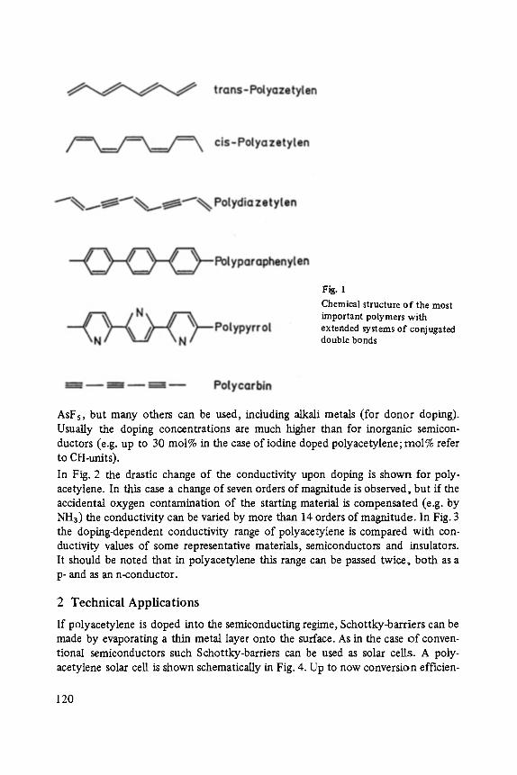
Fig. 1 Chemical structure of the most important polymers with extended systems of conjugated double bonds
AsFs, but many others can be used, including alkali metals (for donor doping). UsuaUy the doping concentrations are much higher than for inorganic semicon- ductors (e.g. up to 30 mol% in the case of iodine doped polyacetylene; tool% refer to CH-units).
In Fig. 2 the drastic change of the conductivity upon doping is shown for poly- acetylene. In this case a change of seven orders of magnitude is observed, but if the accidental oxygen contamination of the starting material is compensated (e.g. by NHa) the conductivity can be varied by more than 14 orders of magnitude. In Fig. 3 the doping-dependent conductivity range of polyacetylene is compared with con- ductivity values of some representative materials, semiconductors and insulators. It should be noted that in polyacetylene this range can be passed twice, both as a p- and as an n-conductor.
2 T e c h n i c a l Appl i ca t ions
If polyacetylene is doped into the semiconducting regime, Schottky-barriers can be made by evaporating a thin metal layer onto the surface. As in the case o f conven- tional semiconductors such Schottky-barriers can be used as solar cells. A poly- acetylene solar cell is shown schematically in Fig. 4. Up to now conversion efficien-
120

Fig. 2
Conductivity of trans-polyacetylene over acceptor doping at room temper- ature
Fig. 3
Comparison of the conductivity obtainable in polyacetylene with that of other materials
121
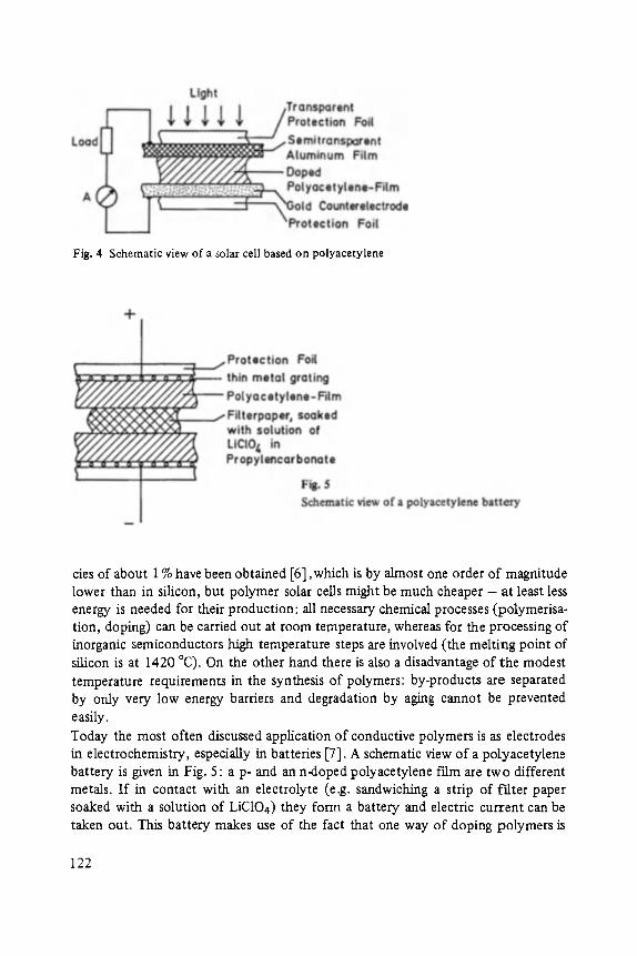
Fig. 4 Schematic view of a solar cell based on polyacetylene
cies of about 1% have been obtained [6] ,which is by almost one order of magnitude lower than in silicon, but polymer solar ceils might be much cheaper - at least less energy is needed for their production: all necessary chemical processes (polymerisa- tion, doping) can be carried out at room temperature, whereas for the processing of inorganic semiconductors high temperature steps are involved (the melting point of silicon is at 1420 ~ On the other hand there is also a disadvantage of the modest temperature requirements in the synthesis of polymers: by-products are separated by only very low energy barriers and degradation by aging cannot be prevented easily. Today the most often discussed application of conductive polymers is as electrodes in electrochemistry, especially in batteries [7]. A schematic view of a polyacetylene battery is given in Fig. 5: a p- and an n-doped polyacetylene film are two different metals. If in contact with an electrolyte (e.g. sandwiching a strip of filter paper soaked with a solution of LiC104) they form a battery and electric current can be taken out. This battery makes use of the fact that one way of doping polymers is
122
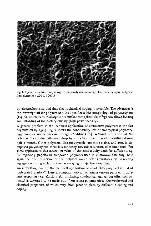
Fig. 6 Open, fleece-like morphology of polyacetylene (scanning electromicrograph). A typical fiber diameter is 200 to 1000 k
by electrochemistry and that electrochemical doping is reversible. The advantage is the low weight of the polymer and the open fleece-like morphology of polyacetylene (Fig. 6), which leads to alarge inner surface area (about 60 m~/g) and allows loading and unloading of the battery quickly (high power density).
A general problem in the technical apphcation of conductive polymers is the fast degradation by aging. Fig. 7 shows the conductivity loss of two typical polyacety- lene samples under various storage conditions [8]. Without protection of the polymer the conductivity may drop by more than one order of magnitude during half a month. Other polymers, like polypyrrole, are more stable, and even in air- exposed polyacetylene there is a tendency towards saturation after some time. For some applications this saturation value of the conductivity could be sufficient, e.g. for replacing graphite in compound polymers used in microwave shielding: here again the open structure of the polymer would offer advantages by preventing segregation during such processes as spraying or injection-moulding.
An interesting idea for the technical application of conductive polymers is that of "integrated plastics". Here a complex device, containing various parts with diffe- rent properties (e.g. elastic, rigid, insulating, conducting, and various other compo- nents) is supposed to be made out of one single polymer piece, the mechanical and electrical properties of which vary from place to place by different blending and doping.
123
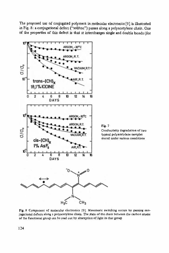
The proposed use of conjugated polymers in molecular electronics [9] is illustrated in Fig. 8: a conjugational defect ("sol i ton") passes along a polyacetylene chain, One of the properties of this defect is that it interchanges single and double bonds (for
Fig. 7 Conductivity degradatio n of two typical polyacetylene samples stored under various conditions
Fig. 8 Component of molecular electronics [9]. Mesomeric switching occurs by passing con- jugational defects along a polyaeetylene chain. The state of the chain between the carbon atoms of the functional group can be read out by absorption of light in that group
124

more details see Ref. [2-5]) . The mesomeric state of the conjugated chain can be read out by the help of special functional groups, which mark two neighbouring chain sites. One such group is shown in the figure: by the absorption of light this group can go into an excited state, but it can absorb light only if the bonds are arranged in such a way that there is a double bond between the group's central carbon atoms.
3 Electr ical Conduc t iv i ty
It has been argued that the exciting physics of extended systems of conjugated double bonds and in particular the possible existence of mobile conjugational defects (solitons) might lead to a new mechanism of electrical conductivity in polymers. Fig. 9 shows the temperature dependence of the DC conductivity of polyacetylene doped with various concentrations of iodine [10]. We observe quali-
Fig. 9 Temperature dependence of the DC conductivity of polyacetylene doped with various concentrations of iodine [101
125

tatively similar behaviour for all polymers investigated so far (trans-polyacetylene, cis-polyacetylene, polypyrrole) and for all dopants used (iodine, AsFs, FeCIa in polyacetylene, BE4 in polypyrrole), although there are some differences in detail. These differences seem to depend more on the dopant than on the polymer. The curves of Fig. 9 look very similar to the conductivity data one usually obtaines in highly disordered metals (high iodine concentrations) or in doped amorphous semiconductors (low iodine concentration in Fig. 9). We succeed in explaining our results on highly doped polyacetylene by fluctuation induced tunneling (which is found in granular metals) [11 ] and at low doping levels by variable range hopping (found in amorphous semiconductors). Specific features of 1-d metals (solitons) cannot be seen in our conductivity data.
Fig. 10 presents a schematized view of the morphology ofpolyacetylene: there is a hierarchy of inhomogeneities. Polymer chains are arranged to microcrystals and the microcrystals arrange to fibers. There are point defects (infinite barriers in 1 -d) in the microcrystals and amorphous regions between the microcrystals. The fibers are only in loose electrical contact with one another, giving rise to large inner con- tact resistances. Four hypothetical microprobes are shown in the figure: 1 and 2 on the same polymer chain, 3 on a different chain and 4 on a different fiber. Only the transport from 1 to 2 would show 1 - d features, but no experimental situation can be arranged where this transport dominates the overall electrical resistance.
For samples with high dopant concentrations (above 10 % iodine), we assume that the interfibrillar contact resistance is dominating. In this regime we can excellently fit our data by assuming fluctuation induced tunneling [11] through the contact barriers as shown in Fig. 11 [12].
Fig. 10 Schematized view of the morphology of polyacctylene (compare the electro- micrographs of Fig. 6)
126
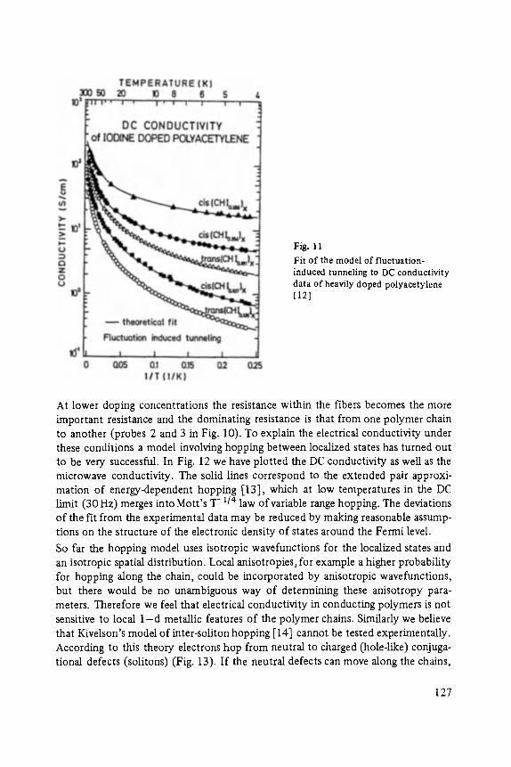
Fis. 11 Fit of the model of fluctuation= induced tunneling to DC conductivity data of heavily doped polyacetylene [121
At lower doping concentrations the resistance within the fibers becomes the more important resistance and the dominating resistance is that from one polymer chain to another (probes 2 and 3 in Fig. 10). To explain the electrical conductivity under these conditions a model involving hopping between localized states has turned out to be very successful. In Fig. 12 we have plotted the DC conductivity as well as the microwave conductivity. The solid lines correspond to the extended pair approxi- mation of energy-dependent hopping [13], which at low temperatures in the DC limit (30 Hz) merges into Mott's T- 1/4 law of variable range hopping. The deviations of the fit from the experimental data may be reduced by making reasonable assump- tions on the structure of the electronic density of states around the Fermi level.
So far the hopping model uses isotropic wavefunctions for the localized states and an isotropic spatial distribution. Local anisotropies, for example a higher probability for hopping along the chain, could be incorporated by anisotropic wavefunctions, but there would be no unambiguous way of determining these anisotropy para- meters. Therefore we feel that electrical conductivity in conducting polymers is not sensitive to local 1 - d metallic features of the polymer chains. Similarly we believe that Kivelson's model of inter-sohton hopping [14] cannot be tested experimentally. According to this theory electrons hop from neutral to charged (hole4ike) conjuga- tional defects (solitons) (Fig. 13). If the neutral defects can move along the chains,
127
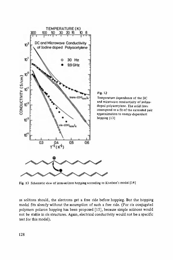
Fig. 12 Temperature dependence of the DC and microwave conductivity of iodine- doped polyacetylene. The solid lines correspond to a fit of the extended pair approximation to energy-dependent hopping [13]
Fig. 13 Schematic view of inter-soliton hopping according to Kivelson's model [14]
as solitons should, the electrons get a free ride before hopping. But the hopping model fits already without the assumption of such a free ride. (For cis conjugated polymers polaron hopping has been proposed [15], because simple solitons would not be stable in cis structures. Again, electrical conductivity would not be a specific test for this model).
128

Polyacetylene trims can be stretch-oriented up to a certain degree. Then the fibers are more or less aligned. In such stretched fttms a macroscopic anisotropy of the electrical conductivity is observed. This is not surprising because there are less con- tact barriers per unit length along the stretch axis. The anisotropy changes with temperature, as we show in Fig. 14. This temperature dependence of the aniso- tropy is difficult to understand. Because we do not contact an individual fiber but the whole fleece, the source of the measured anisotropy cannot be a local 1 - d behaviour of the polymer chains (the current must always flow along the fiber, no matter how the charged carriers hop in detail). It is tempting to attribute the temperature dependence of the anisotropy to a temperature dependence of non- linearities in the I-V-characteristics of the contact barriers; but nonlinear barriers would lead to deviations from Ohm's law in the overalI conductivity - strict ohmicity, however, is observed at the voltage used in the measurement of Fig. 14.
Fig. 14 Temperature dependence of the macroscopic anisotropy of the electrical conductivity of iodine-doped partially stretch-oriented trans-polyacetylene
129
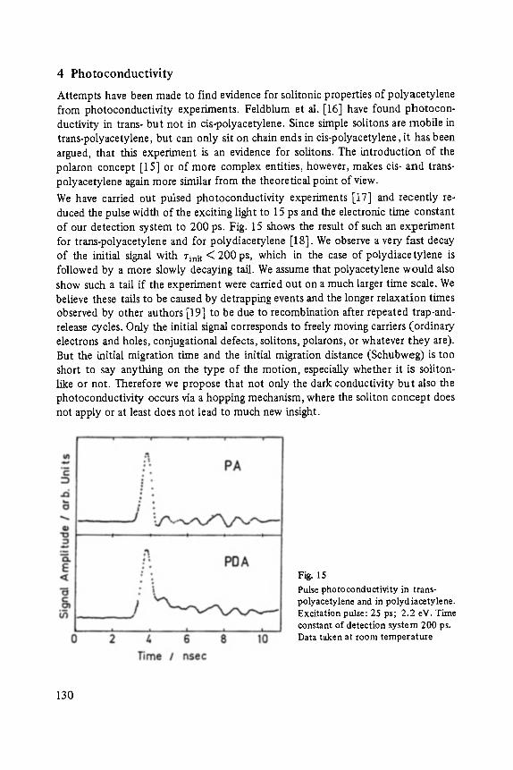
4 P h o t o c o n d u c t i v i t y
Attempts have been made to find evidence for solitonic properties of polyacetylene from photoconductivity experiments. Feldblum et al. [16] have found photocon- ductivity in trans- but not in cis-polyacetylene. Since simple solitons are mobile in trans-polyacetylene, but can orfly sit on chain ends in cis-polyacetylene, it has been argued, that this experiment is an evidence for solitons. The introduction of the polaron concept [15] or of more complex entities, however, makes cis- and trans- polyacetylene again more similar from the theoretical point of view.
We have carried out pulsed photoconductivity experiments [17] and recently re- duced the pulse width of the exciting light to 15 ps and the electronic time constant of our detection system to 200 ps. Fig. 15 shows the result of such an experiment for trans-polyacetylene and for polydiacetylene [18]. We observe a very fast decay of the initial signal with 7init ( 2 0 0 p s , which in the case of potydiacetylene is followed by a more slowly decaying taft. We assume that polyacetylene would also show such a tail if the experiment were carried out on a much larger time scale. We believe these tails to be caused by detrapping events and the longer relaxation times observed by other authors [19] to be due to recombination after repeated trap-and- release cycles. Only the initial signal corresponds to freely moving carriers (ordinary electrons and holes, conjugational defects, solitons, polarons, or whatever they are). But the initial migration time and the initial migration distance (Schubweg) is too short to say anything on the type of the motion, especially whether it is sohton- like or not. Therefore we propose that not only the dark conductivity but also the photoconductivity occurs via a hopping mechanism, where the soliton concept does not apply or at least does not lead to much new insight.
Fig. 15 Pulse photoconductivity in trans- polyacetylene and in polydiacetylene. Excitation pulse: 25 ps; 2.2 eV. Time constant of detection system 200 ps. Data taken at room temperature
130
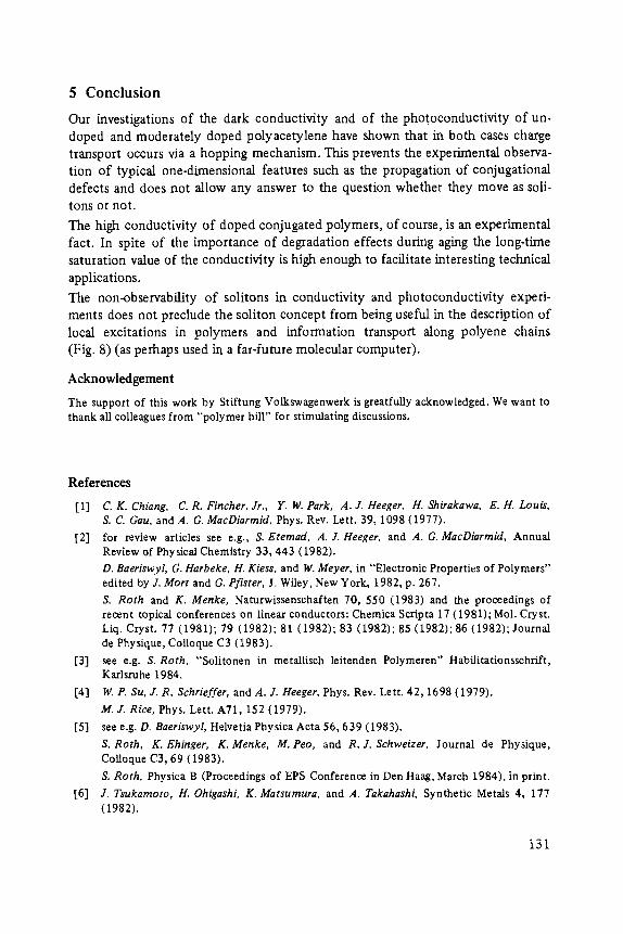
5 C o n c l u s i o n
Our investigations o f the dark conductivity and o f the photoconduct ivi ty o f un- doped and moderately doped polyacetylene have shown that in both cases charge transport occurs via a hopping mechanism. This prevents the experimental observa- t ion of typical one-dimensional features such as the propagation of conjugational defects and does not allow any answer to the question whether they move as soli-
tons or not.
The high conductivity of doped conjugated polymers, of course, is an experimental fact. In spite of the importance o f degradation effects during aging the long-time saturation value of the conductivity is high enough to facilitate interesting technical
applications.
The non-observability of solitons in conductivity and photoconduct ivi ty experi- ments does not preclude the soliton concept from being useful in the description of local excitations in polymers and information transport along polyene chains (Fig. 8) (as perhaps used in a far-future molecular computer).
Acknowledgement
The support of this work by Stfftung Volkswagenwerk is greatfully acknowledged. We want to thank all colleagues from "polymer hill" for stimulating discussions.
References
[1] C.K. Chiang, C R. Fincher, Jr., Y. W. Park, A. J. Heeger, H. Shirakawa, E. H. Louis, S. C. Gau, andA. G. MacDiarmid, Phys. Rev. Lett. 39, 1098 (1977).
[2] for review articles see e.g., S. Etemad, A. J. Heeger, and A. G. MacDiarraid, Annual Review of Physical Chemistry 33,443 (1982). D. Baeriswyl, G. Harbeke, H. Kiess. and W. Meyer, in "Electronic Properties of Polymers" edited by J. Mort and G. Pfister, J. Wiley, New York, 1982, p. 267. S. Roth and K. Menke, Naturwissenschaften 70, 550 (1983) and the proceedings of recent topical conferences on lineax conductors: Chemica Scripta 17 (1981); Mol. Cryst. Liq. Cryst. 77 (1981); 79 (1982); 81 (1982); 83 (1982); 85 (1982); 86 (1982); Journal de Physique, CoIloque C3 (1983).
[3] see e.g.S. Roth, "Solitonen in metallisch leitenden Polymeren" Habilitationsschrift, Karlsruhe 1984.
[4] W.P. Su, J. R. Schrieffer, and A. J. Heeger, Phys. Rev. Lett. 42, 1698 (1979). M. J. Rice, Phys. Lett. A71, 152 (1979).
[5] see e.g.D. Baeriswyl, Helvetia Physica Acta 56,639 (1983). S. Roth, K. Ehinger, K. Menke, M. Peo, and R. J. Schweizer, Journal de Physique, CoUoque C3, 69 (1983). S. Roth, Physica B (Proceedings of EPS Conference in Den Haag, March 1984), in print.
[6] J. Tsukamoto, H. Ohigashi, K. Matsumura, and A. Takahashi, Synthetic Metals 4, 177 (1982).
131
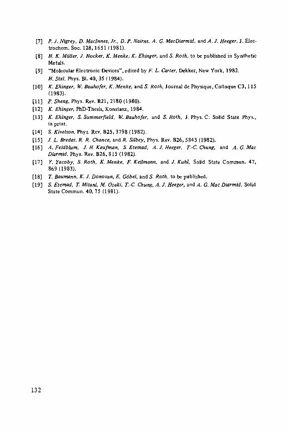
[7] P, J. Nigrey, D. Maclnnes, Jr., D. P. Nairns, A. G. MacDiarmid, and A. J. Heeger, I. Elec- trochem. Soc. 128, 1651 (1981).
[8] H. K. Mailer, J. Hocker, K. Menke, K. Ehinger, and S. Roth, to be published in Synthetic Metals.
[9] "Molecular Electronic Devices", edited by F. L. Carter, Dekker, New York, 1982.
1"1. Sixl, Phys. BI. 40, 35 (1984).
[10] K. Ehinger, W. Bauhofer, K. Menke, and S. Roth, Journal de Physique, Colloque C3, 115 (1983).
[11] P. Sheng, Phys. Rev. B21, 2180 (1980).
[12] K. Ehinger, PhD-Thesis, Konstanz, 1984.
[13] K. Ehinger, S. Summerfield, W. Bauhofer, and S. Roth, J. Phys. C: Solid State Phys., in print.
[14] S. Kivelson, Phys. Rev. B25, 3798 (1982).
[15] J. L. Breclas, R. R. Chance, and R. Silbey, Phys. Rev. B26, 5843 (1982). [16] A. FeMblum, J. H. Kaufman, S. Eternad, A. J. Heeger, T.-C. Chung, and A. G. Mac
Diarmid, Phys. Rev. B26, 815 (1982).
[17] Y. Yacoby, S. Roth, K. Menke, F. Keilmann. and J. Kuhl, Solid State Commun. 47, 869 (1983).
[18] T. Baumann, K. J. Donovan, E. G6bel, and S. Roth, to be published.
[19] S. Etemad, T. Mitani, M. Ozaki, T.-C. Chung, A. J. Heeger, and A. G. Mac Diarmid, Solid State Commun. 40, 75 (1981).
132

Transport and Recombination in Hydrogenated Amorphous Silicon
Walther Fuhs
Fachbereich Physik, Universit~it Marburg, Marburg, Federal Republic of Germany
Summary: In the field of amorphous semiconductors hydrogenated amorphous silicon (a-Si: H) is of particular interest both for research and application owing to its low density of defect states in the gap. This paper reviews important aspects of transport and recombination of excess carriers in glow discharge deposited a-Si:H. Special emphasis is given to the still unsolved problem of tight induced defects.
1 I n t r o d u c t i o n
A glance at the program of the last international conferences on amorphous semi- conductors shows that hydrogenated amorphous silicon (a-Si:H) plays a pre- dominant role in this field. The reason is that amorphous silicon holds considerable promise for exciting technical applications, e.g. in solar cells, field effect transistors, optoelectronic devices, and xerography. In addition a study of this material is expected to help to obtain a better understanding of the physics of disordered materials in general.
Amorphous silicon prepared by conventional evaporation or sputtering contains large defect densities and a network of microvoids. A breakthrough was the use of the glow discharge deposition technique [ 1] by decomposing Sill4 in the electric field of a discharge. The achieved progress was that glow discharge deposited films have a much lower density of defect states in the gap owing to bond saturation by hydrogen atoms. Similar film properties have also been obtained by other hydro- genation techniques: sputtering in inert gas containing hydrogen [2, 3], post-hydro- genation of evaporated or sputtered films [4], chemical vapor deposition from Sill4 [5, 6]. To date the glow discharge decomposition leads to films of superior semi- conducting and photoelectric properties.
The glow discharge deposited films contain 4 - 4 0 at% hydrogen depending on the deposition parameters in particular on the deposition temperature [7]. All prop- erties depend on the H-content and thus on the details of the deposition process. The films of best semiconductor quality are deposited at temperatures 220-280 ~ and contain 4 - 10 at% hydrogen. Annealing of the films at temperatures above the deposition temperature leads to the evolution of hydrogen [8], Hydrogen bonding
133
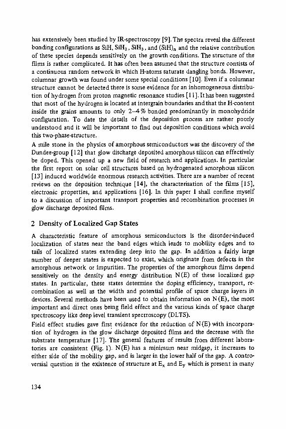
has extensively been studied by IR-spectroscopy [9]. The spectra reveal the different bonding configurations as Sill, Sill2, SiHa, and (SiH)n and the relative contribution of these species depends sensitively on the growth conditions. The structure of the films is rather complicated. It has often been assumed that the structure consists of a continuous random network in which H-atoms saturate dangling bonds. However, columnar growth was found under some special conditions [10]. Even if a columnar structure cannot be detected there is some evidence for an inhomogeneous distribu- tion of hydrogen from proton magnetic resonance studies [ 11 ]. It has been suggested that most of the hydrogen is Iocated at intergrain boundaries and that the H-content inside the grains amounts to only 2 - 4 % bonded predominantly in monohydride configuration. To date the details of the deposition process are rather poorly understood and it will be important to find out deposition conditions which avoid this two-phase-structure.
A mile stone in the physics of amorphous semiconductors was the discovery of the Dundee-group [12] that glow discharge deposited amorphous silicon can effectively be doped. This opened up a new field of research and applications. In particular the first report on solar cell structures based on hydrogenated amorphous silicon [ 13] induced worldwide enormous research activities. There are a number of recent reviews on the deposition technique [14], the characterisation of the f'flms [15], electronic properties, and applications [16]. In this paper I shall confine myself to a discussion of important transport properties and recombination processes in glow discharge deposited films.
2 Densi ty o f Local ized Gap States
A characteristic feature of amorphous semiconductors is the disorder-induced localization of states near the band edges which leads to mobility edges and to tails of localized states extending deep into the gap. In addition a fairly large number of deeper states is expected to exist, which originate from defects in the amorphous network or impurities. The properties of the amorphous films depend sensitively on the density and energy distribution N(E) of these localized gap states. In particular, these states determine the doping efficiency, transport, re- combination as weU as the width and potential profile of space charge layers in devices. Several methods have been used to obtain information on N (E), the most important and direct ones being field effect and the various kinds of space charge spectroscopy like deep level transient spectroscopy (DLTS).
Field effect studies gave first evidence for the reduction of N (E) with incorpora- tion of hydrogen in the glow discharge deposited films and the decrease with the substrate temperature [17]. The general features of results from different labora- tories are consistent (Fig. 1). N(E) has a minimum near midgap, it increases to either side of the mobility gap, and is larger in the lower half of the gap. A contro- versial question is the existence of structure at Ex and Ey which is present in many
134

Fig. 1 Field effect density of states distribution N(E) of a-Si: H: Curve 1 [171, curve 2 [18]. Arrows indicate the position of the Fermi level.
field effect data [17, 19]. There are a number of problems which raise doubt that the field effect measures the bulk density of states. Current drift by ion motion in the dielectric or deep trapping in the amorphous fdm may lead to transient behaviour, the band bending at zero gate potential is unknown, the films might be inhomogeneous and more importantly, the current path is confined to a narrow channel of 20-100 A width at the interface [15]. Since this part of the film is deposited in the early stage of ffilm growth it might be quite different from the bulk.
The ability to prepare reliable device structures enabled the application of space charge spectroscopy. The analysis of such data is more complex than in crystalline semiconductors because of the continuous distribution of defect states which, among other complications, leads to non-parabolic potential profiles in the space charge layers. In a DLTS-experirnent a non-equilibrium charge is induced by laser excitation or voltage pulses in the depletion region of a Schottky-barrier. The resultant transients of current or capacitance which arise when the trapped carriers are reemitted, are recorded as a function of temperature. The N (E) derived from such studies is significantly different from the field effect density of states (Fig. 2). Generally N (E) is lower and the general shape is dominated by a deep minimum 0.3-0.6 eV below the conduction band with N (E) < 1016 c m -3 e V -1 . There is some disagreement in the data for the lower half of the gap. Whereas the results obtained by laser excitation of n-type samples (curve JH 152 [20]) show a broad shoulder extending from the valence band to midgap, the N(E) obtained from Schottky barriers on p-type ffil s excited by voltage pulses indicate the existence of a mini- mum also in the lower half of the gap (curve 4,5 [21]). Generally the analysis of
135
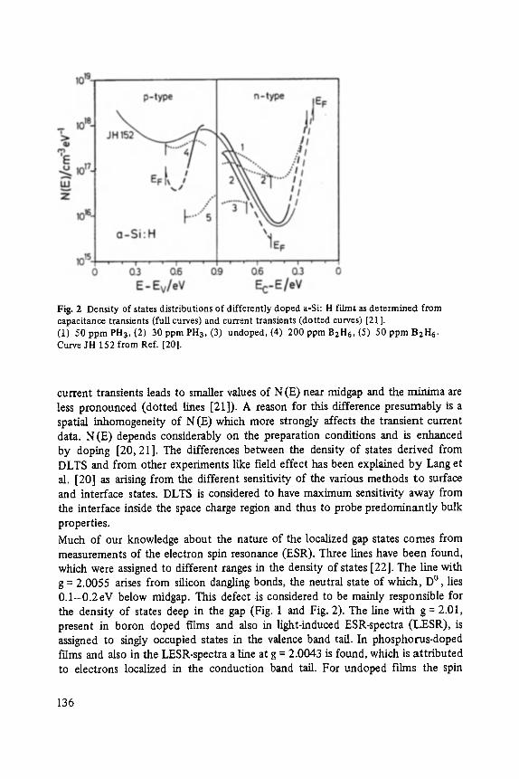
Fig. 2 Density of states distributions of differently doped a-Si: H films as determined from capacitance transients (full curves) and current transients (dotted curves) [21 ]. (1) 50 ppm PH 3, (2) 30 ppm PH a, (3) undoped, (4) 200 ppm B2H6, (5) 50 ppm B2H6. Curve JH 152 from Ref. [201.
current transients leads to smaller values of N (E) near midgap and the minima are less pronounced (dotted lines [21]). A reason for this difference presumably is a spatial inhomogeneity of N (E) which more strongly affects the transient current data. N (E) depends considerably on the preparation conditions and is enhanced by doping [20, 21]. The differences between the density of states derived from DLTS and from other experiments like field effect has been explained by Lang et al. [20] as arising from the different sensitivity of the various methods to surface and interface states. DLTS is considered to have maximum sensitivity away from the interface inside the space charge region and thus to probe predominantly bulk properties.
Much of our knowledge about the nature of the localized gap states comes from measurements of the electron spin resonance (ESR). Three lines have been found, which were assigned to different ranges in the density of states [22]. The line with g = 2.0055 arises from silicon dangling bonds, the neutral state of which, D o , lies 0.1-0.2 eV below midgap. This defect is considered to be mainly responsible for the density of states deep in the gap (Fig. 1 and Fig. 2). The line with g = 2.01, present in boron doped films and also in light-induced ESR-spectra (LESR), is assigned to singly occupied states in the valence band tail. In phosphorus-doped films and also in the LESR-spectra a line at g = 2.0043 is found, which is attributed to electrons localized in the conduction band tail. For undoped films the spin
136
density Ns of the dangling bond line is a reliable measure of the film quality. Ns is strongly influenced by the preparation conditions, particle bombardment and hydrogen effusion and ranges from 10 Is cm -3 to 3" 1019 c m -3 [23, 24]. This line is also found in a-Si prepared by other techniques. From a detailed study of the influence of doping [25] and temperature [26] on the ESR-spectra, Dersch et al. deduced a positive correlation energy of U = 0.4 eV for the dangling bond states and o f about 0.2eV for the valence band tail states. The correlation energy of the conduction band tail states is estimated to be much smaller, namely U ~ 0.01 eV. These different values indicate that the valence band tail states are stronger localized than the states in conduction band tail.
3 T ranspor t Proper t ies
It is generally assumed that in an amorphous semiconductor the electronic states are delocalized inside the bands and become localized below some energy Ec in the conduction band and above Ev in the valence band [27]. Carriers in states above these mobility edges Ec and Ev are supposed to have mobilities near 10 cm2/Vs. Electrons in localized states can contribute to conduction with much lower mobility by thermally activated tunnelling. The existence of sharp mobility edges is still a matter of debate and has been questioned recently considering strong electron- phonon coupling [28, 29]. If the density of states near the Fermi level is high, variable range hopping may be observed with a characteristic temperature depend- ence of the conductivity, In a ~ - ( T o / T ) 1/4 [27]. In hydrogenated a-Si, where the density of gap states is low, transport is considered to occur predominantly above the mobility edges Er and Ev. In this chapter, I shall concentrate on a discussion of measurements of conductivity a(T) and thermoelectric power S(T). At present the understanding of the Hall effect appears too uncomplete to allow meaningful conclusions. Generally a sign anomaly is observed which means that the sign of the Hall effect is opposite to that of the predominating carriers i.e. positive for trans- port by electrons [30, 31 ].
If transport is by electrons near the mobility edge Ec the conductivity a and ther- moelectric power S are given by
( E e - E F ~ a = ao(T) exp kT / (1)
S E c - E ~ k = ~ e T + e A (T) (2)
In these expressions k denotes the Boltzmann constant and E F the Fermi energy. Corresponding expressions are valid for hole conduction at Ev. a0 depends on the mobility and N (Ec) and A (T) is related to the kinetic energy of the carriers. The theory of minimum metallic conductivity [32] predicts for the conductivity pre- factor O'mi n ~ 200 ~2 -1 cm -1 and A = 1. If one considers the shrinking of the band
137
gap caused by electron phonon coupling which is evident from the temperature dependence of the optical energy gap, tile prefactor is increased by about a factor of 10 [33]. This leads to a0 ~ 2000 a - i cm-l. The problem in the analysis of the experimental data is that both ao and A may depend on temperature, likewise the Fermi energy EF and the position of the mobility edge Ee. As a consequence the extrapolations of the experimental o (T) and S (T)-curves do not give o0 and A. Furthermore the apparent activation energies of conductivity and thermoelectric power, Ea and Es, will be different from E c - EF. Beyer and Overhof have given a detailed description of these complications [34]. If for instance there is a linear dependence of the Fermi level on temperature
E F (T) = E} - ~T (3)
one finds using the expressions (1) and (2)
* �9 A * k or0 = eo e-n/k, = e A + e-" Ea = (Ec - E}) (4)
Generally, Eo will thus be different from the actual Ec - EF, instead it is equal to E c - E ~ at T = 0 K . A breakthrough in the physics of amorphous semiconductors was the discovery that amorphous Si prepared by glow discharge decomposition can effectively be doped by adding controlled amounts of PHB or B2H6 to the SiI-h in the discharge [12, 17]. The failure of earlier attempts to dope amorphous semiconductors had been explained by Mott [35] who suggested that in an amorphous network impurity atoms have a local environment which allows to take up all electrons in bonds. This rule obviously is not strictly obeyed and at least part of the dopant atoms are elec- trically active. The first direct evidence of substitutional doping in a-Si:H was obtained by Knights et al. [36] from EXAFS (Extended X-Ray Absorption Fine Structure)-investigations. It was found that the increase of the conductivity on arsenic incorporation is correlated with the number of four-fold coordinated arsenic atoms and that only about 20% of the arsenic atoms are incorporated in this configuration. Using the field effect density of states Spear and LeComber [37] estimated the doping efficiency of phosphorus from ion probe analysis to 0.3-0.4. Generally the concentration of incorporated dopant atoms in the film is different from the concentration in the gas phase. Widely different values are given in the literature for the incorporation ratio. For phosphorus doping the values range from 0.5 [37] to 5.2 [38] and for boron doping from below 0.5 [37] to 4.8 [39]. In an amorphous semiconductor most of the donors deliver their electrons to empty states near the Fermi level. The resultant shift of the Fermi level, therefore, de- pends on the density of states. The doping effect in a-Si: H thus is closely" related to the low density of defect states in the hydrogenated films. Results for doping from the gas phase of various laboratories are shown in Fig. 3. For P-doping the maxi- mum conductivity of about 10 -2 ~2 -1 cm -1 is attained at 103 - 104 ppmPH3. At
138
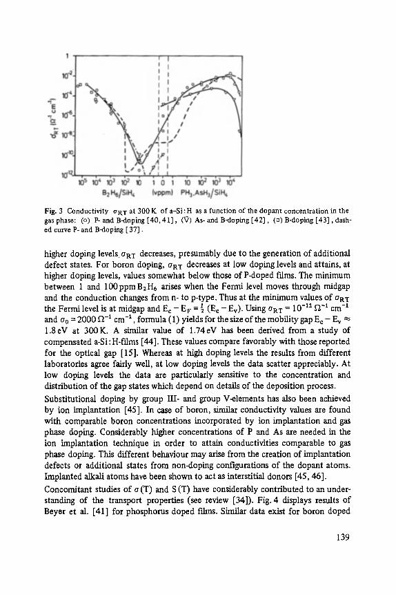
Fig. 3 Conductivity ORT at 300 K of a-Si:H as a function of the dopant concentration in the gas phase: (o) P- and B-doping [40, 41], (~) As- and B-doping [42], (r~) B-doping [43], dash- ed curve P- and B-doping [ 37].
higher doping levels aRT decreases, presumably due to the generation of additional defect states. For boron doping, aRT decreases at low doping levels and attains, at higher doping levels, values somewhat below those of P-doped f'tlms. The minimum between 1 and 100ppmB2H6 arises when the Fermi level moves through midgap and the conduction changes from n- to p-type. Thus at the minimum values of aRT
10-12 fl-1 the Fermi level is at midgap and E c - E~- = ~ (E e - Ev). Using aRT = cm -1 and oo = 2000 f1-1 cm -I , formula (1) yields for the size of the mobility gap Ec - F-.v ~ 1.8 eV at 300 K. A similar value of 1.74 eV has been derived from a study of compensated a-Si: H-fdrns [44]. These values compare favorably with those reported for the optical gap [15]. Whereas at high doping levels the results from different laboratories agree fairly well, at low doping levels the data scatter appreciably. At low doping levels the data are particularly sensitive to the concentration and distribution of the gap states which depend on details of the deposition process.
Substitutional doping by group III- and group V-elements has also been achieved by ion implantation [45]. In case of boron, similar conductivity values are found with comparable boron concentrations incorporated by ion implantation and gas phase doping. Considerably higher concentrations of P and As are needed in the ion implantation technique in order to attain conductivities comparable to gas phase doping. This different behaviour may arise from the creation of implantation defects or additional states from non-doping configurations of the dopant atoms. Implanted alkali atoms have been shown to act as interstitial donors [45, 46].
Concomitant studies of o (T) and S (T) have considerably contributed to an under- standing of the transport properties (see review [34]). Fig. 4 displays results of Beyer et al. [41] for phosphorus doped films. Similar data exist for boron doped
139
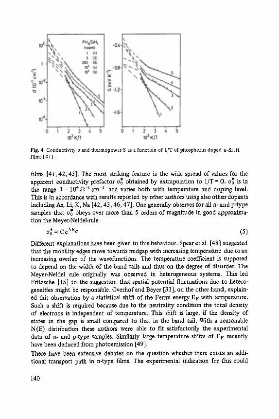
Fig. 4 Conductivity o and thermopower S as a function of 1/T of phosphorus doped a-Si: H films [41].
fdms [41, 42, 43]. The most striking feature is the wide spread of values for the apparent conductivity prefactor a* obtained by extrapolation to 1/T = O. a* is in the range 1 -104 g2 -1 cm -1 and varies both with temperature and doping level. This is in accordance with results reported by other authors using also other dopants including As, Li, K, Na [42, 43, 46, 47]. One generally observes for all n- and p-type samples that u* obeys over more than 5 orders of magnitude in good approxima- tion the Meyer-Neldel-rule
oF -- C e AEo (5)
Different explanations have been given to this behaviour. Spear et al. [48] suggested that the mobility edges move towards midgap with increasing temperature due to an increasing overlap of the wavefunctions. The temperature coefficient is supposed to depend on the width of the band tails and thus on the degree of disorder. The Meyer-Neldel rule originally was observed in heterogeneous systems. This led Fritzsche [15] to the suggestion that spatial potential fluctuations due to hetero- geneities might be responsible. Overhof and Beyer [33], on the other hand, explain- ed this observation by a statistical shift of the Fermi energy E~- with temperature. Such a shift is required because due to the neutrality condition the total density of electrons is independent of temperature. This shift is large, if the density of states in the gap is small compared to that in the band tail. With a reasonable N(E) distribution these authors were able to fit satisfactorily the experimental data of n- and p-type samples. Similarly large temperature shifts of EF recently have been deduced from photoemission [49].
There have been extensive debates on the question whether there exists an addi- tional transport path in n-type f'rims. The experimental indication for fhis could
140
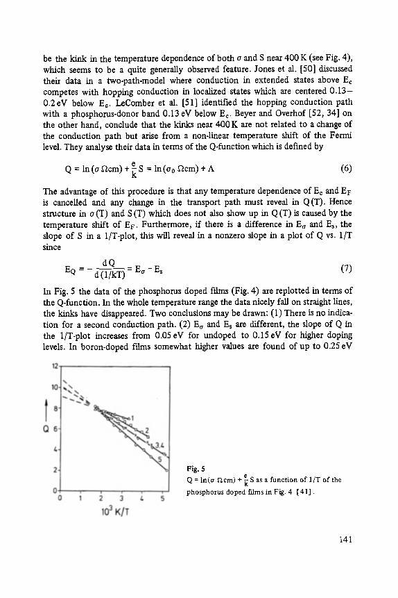
be the kink in the temperature dependence of both a and S near 400 K (see Fig. 4), which seems to be a quite generally observed feature. Jones et al. [50] discussed their data in a two-path-model where conduction in extended states above Er competes with hopping conduction in localized states which are centered 0 .13- 0.2 eV below Ec. LeComber et al. [51] identified the hopping conduction path with a phosphorus-donor band 0.13 eV below Ec. Beyer and Overhof [52, 34] on the other hand, conclude that the kinks near 400 K are not related to a change of the conduction path but arise from a non-linear temperature shift of the Fermi level. They analyse their data in terms of the Q-function which is defined by
e Q = ha (o ~cm) + ~r S : In (o0 f2cm) + A (6)
The advantage of this procedure is that any temperature dependence of Ec and EF is cancelled and any change in the transport path must reveal in Q (T). Hence structure in o (T) and S (T) which does not also show up in Q (T) is caused by the temperature shift of EF. Furthermore, if there is a difference in Ea and Es, the slope of S in a 1/T-plot, this will reveal in a nonzero slope in a plot of Q vs. 1/T since
dQ EQ = d(I /kT) = E o - E s (7)
In Fig. 5 the data of the phosphorus doped t'rims (Fig. 4) are replotted in terms of the Q-function. In the whole temperature range the data nicely fall on straight lines, the kinks have disappeared. Two conclusions may be drawn: (1) There is no indica- tion for a second conduction path. (2) Eo and Es are different, the slope of Q in the 1/T-plot increases from 0.05 eV for undoped to 0.15 eV for higher doping levels. In boron-doped f'flms somewhat higher values are found of up to 0.25 eV
Fig. 5 +e Q = ln(o ~2cm) ~ S as a function of 1/T of the
phosphorus doped trims in Fig. 4 [41].
141

[34]. Such behaviour is observed rather generally for a large variety of doped and undoped films prepared under various conditions. An explanation for the non-vanishing slope of Q (T) has been suggested by D6hler [55] who, starting from the Kubo-Greenwood formalism, considered the energy dependent contribution to conductivity a (E) by hopping transport in the localized band tail states. Such a model in principle may lead to EQ 4: 0, but Q (I") depends sensitively on the assumed o (E) and hence on the shape of N (E). In order to explain the linear dependence of Q on l/T, one has to assume that by doping or a change of the preparation conditions, N (E) is always changed such that it describes the correct slope of Q(T) and retains in addition the linearity of Q in the 1/T-plot. It is this sensitivity of Q (T) to o (E) which makes this model rather unlikely.
Beyer and Overhof [53] proposed that long range static potential fluctuations may lead to EQ 4:0 by causing long range fluctuations of the mobility edges. Such potential fluctuations are supposed to arise from local density fluctuations, growth inhomogeneities or electric fields from charged states [54]. Overhof and Beyer [53] discussed the latter case in detail. They found that in highly doped films the random distribution of ionized donors may cause internal electric fields on a scale of typically 200 A. Their model predicts Ea - Es = 1.25 A, where A is the magnitude of these potential fluctuations. It is important to note that these fluctuations affect the thermoelectric power much more than the conductivity. A computer calculation shows that Ea is decreased by 0.25 A and Es by 1.5 A [34]. It seems difficult to explain the relatively large values of A only by a statistical distribution of charged centers. However, NMR (Nuclear Magnetic Resonance) studies indicate that the a-Si:H films are not homogeneous and large potential fluctuations can originate from all kinds of inhomogeneity.
The detailed investigations on n- and p-type f'rims have shown that the conductivity prefactor or0 is independent of doping and the details of the deposition process and amounts to about 2000 g2 -1 cm -~. The apparent prefactor o*, however, may vary appreciably mainly due to the statistical shift of the Fermi level, ao is practically the same for electron- and hole conduction as one expects from the concept of minimum metallic conductivity [34]. The structure which is often observed in e (I") and S (T) can be explained by a non-linear shift of the Fermi level with temperature. A difference in the activation energies of o and S may arise from long range potential fluctuations due to tnhomogeneities in the films.
There is growing evidence for the creation of deep defect states with doping. These states may be responsible for the decreasing doping efficiency at high doping levels (Fig. 3). Doping induced defect states are observed in transport studies [40] and also in using various techniques as DLTS [20, 21], photothermal deflection spectro- scopy [56], photoacoustic spectroscopy [57], and photoconductivity [58]. Street [59] suggested that defect creation by doping is an inherent feature of the amor- phous structure. Moving the Fermi level towards Ec, defect states are supposed to
142
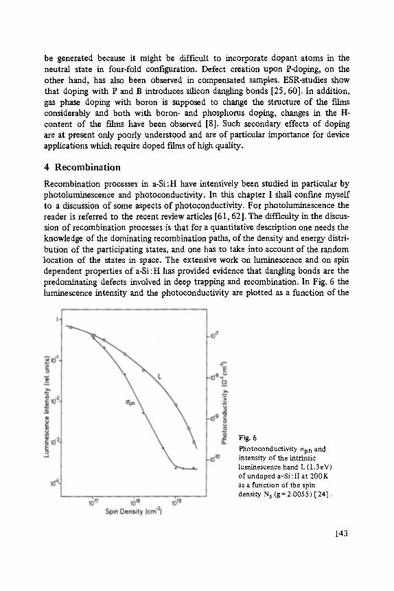
be generated because it might be difficult to incorporate dopant atoms in the neutral state in four-fold configuration. Defect creation upon P-doping, on the other hand, has also been observed in compensated samples. ESR-studies show that doping with P and B introduces silicon dangling bonds [25, 60]. In addition, gas phase doping with boron is supposed to change the structure of the films considerably and both with boron- and phosphorus doping, changes in the H- content of the films have been observed [8]. Such secondary effects of doping are at present only poorly understood and are of particular importance for device applications which require doped t'rims of high quality.
4 R e c o m b i n a t i o n
Recombination processes in a-Si:H have intensively been studied in particular by photoluminescence and photoconductivity. In this chapter I shall toni'me myself to a discussion of some aspects of photoconductivity. For photoluminescence the reader is referred to the recent review articles [61,62]. The difficulty in the discus- sion of recombination processes is that for a quantitative description one needs the knowledge of the dominating recombination paths, of the density and energy distri- bution of the participating states, and one has to take into account of the random location of the states in space. The extensive work on luminescence and on spin dependent properties of a-Si:H has provided evidence that dangling bonds are the predominating defects involved in deep trapping and recombination. In Fig. 6 the luminescence intensity and the photoconductivity are plotted as a function of the
Fig. 6
Photoconductivity ~ph and intensity of the intrinsic luminescence band L (1.3eV) of undoped a-Si :H at 200K as a function of the spin density N s (g= 2.0055) [24].
143
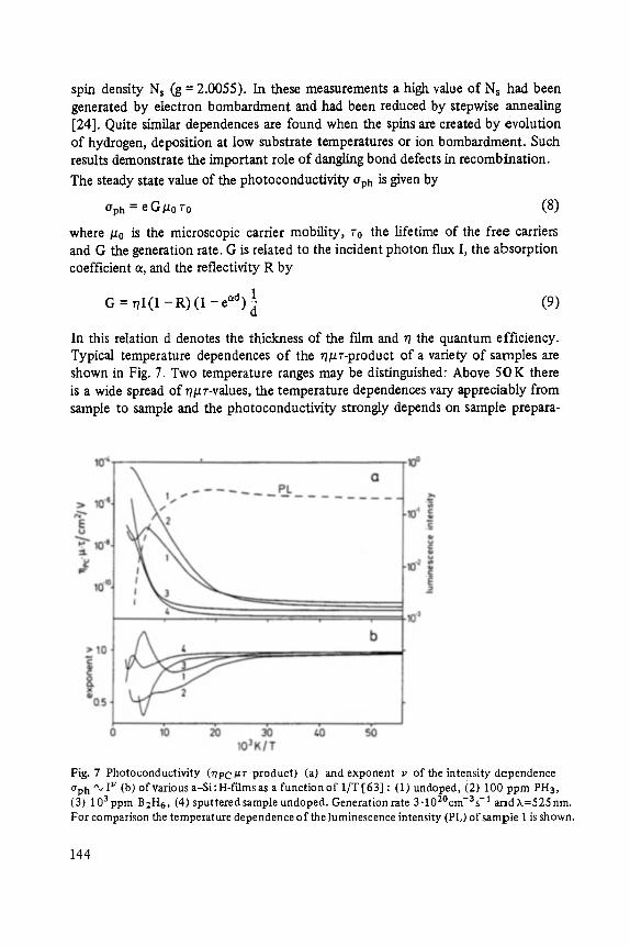
spin density Ns (g = 2.0055). In these measurements a high value of Ns had been generated by electron bombardment and had been reduced by stepwise annealing [24]. Quite similar dependences are found when the spins are created by evolution of hydrogen, deposition at low substrate temperatures or ion bombardment. Such results demonstrate the important role of dangling bond defects in recombination.
The steady state value of the photoconductivity O'ph is given by
O'ph = e a /do 7"0 (8)
where /a0 is the microscopic carrier mobility, ro the lifetime of the free carriers and G the generation rate. G is related to the incident photon flux I, the absorption coefficient a, and the reflectivity R by
1 G = 7/1(1 - R) ( i - e an) ~ (9)
In this relation d denotes the thickness of the f'tim and r? the quantum efficiency. Typical temperature dependences of the r~/~r-product of a variety of samples are shown in Fig. 7. Two temperature ranges may be distinguished: Above 50 K there is a wide spread of r?/~r-values, the temperature dependences vary appreciably from sample to sample and the photoconductivity strongly depends on sample prepara-
Fig. 7 Photoconductivity (~pc~r-product) (a) and exponent v of the intensity dependence aph "~ I v (b) of various a-Si : H-films as a function of 1/T [63] : (1) undoped, (2) 100 ppm PH3,
20 3 1 (3) 103ppm B2H6, (4) sputtered sample undoped. Generation rate 3-10 cm- s- arad2~=525nm. For comparison the temperature dependence of the luminescence intensity (PL) of sample 1 is shown.
144
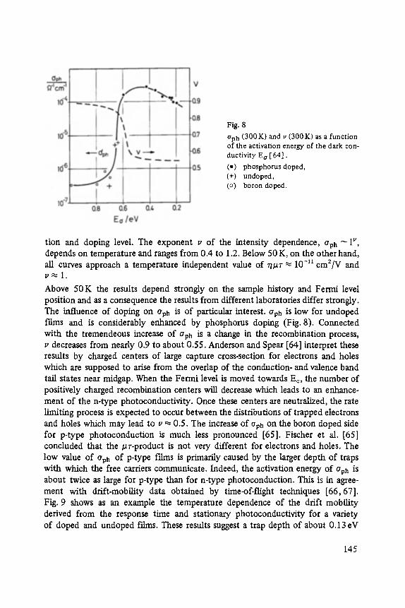
Fig. 8 aph (300K) and v (300K) as a function of the activation energy of the dark con- ductivity E a [ 64]. (o) phosphorus doped, (+) undoped, (o) boron doped.
tion and doping level. The exponent v of the intensity dependence, Oph ~ I v, depends on temperature and ranges from 0.4 to 1.2. Below 50 K, on the other hand, all curves approach a temperature independent value of rT#T ~ l0 -11 cm2/V and v~- l .
Above 50 K the results depend strongly on the sample history and Fermi level position and as a consequence the results from different laboratories differ strongly. The influence of doping on aph is of particular interest, aph is low for undoped f'rims and is considerably enhanced by phosphorus doping (Fig. 8). Connected with the tremendeous increase of aph is a change in the recombination process, v decreases from nearly 0.9 to about 0.55. Anderson and Spear [64] interpret these results by charged centers of large capture cross-section for electrons and holes which are supposed to arise from the overlap of the conduction- and valence band tail states near midgap. When the Fermi level is moved towards Ec, the number of positively charged recombination centers will decrease which leads to an enhance- ment of the n-type photoconductivity. Once these centers are neutralized, the rate limiting process is expected to occur between the distributions of trapped electrons and holes which may lead to v ~ 0.5. The increase of eph on the boron doped side for p-type photoconduction is much less pronounced [65]. Fischer et al. [65] concluded that the pr-product is not very different for electrons and holes. The low value of aph of p-type f'rims is primarily caused by the larger depth of traps with which the free carriers communicate. Indeed, the activation energy of aph is about twice as large for p-type than for n-type photoconduction. This is in agree- ment with drift-mobility data obtained by time-of-flight techniques [66, 67]. Fig. 9 shows as an example the temperature dependence of the drift mobility derived from the response time and stationary photoconductivity for a variety of doped and undoped f'rims. These results suggest a trap depth of about 0.13 eV
145
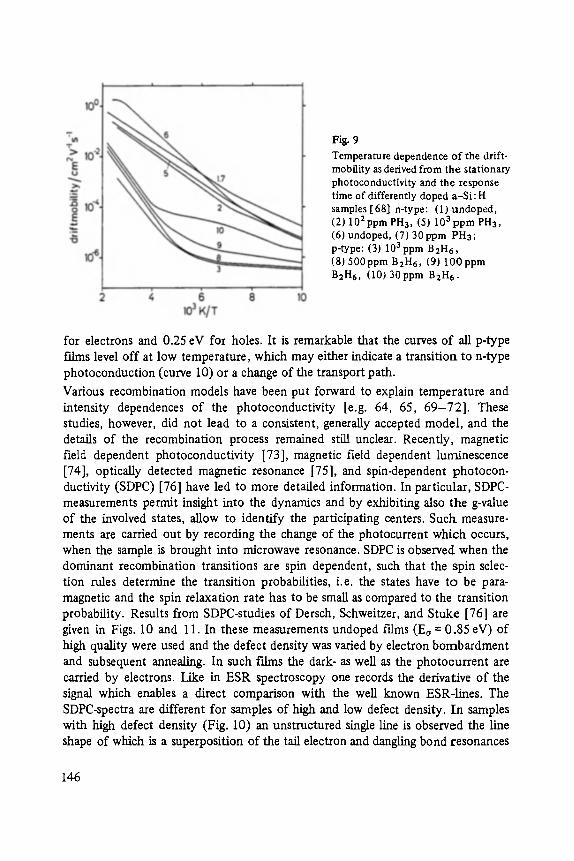
Fig. 9 Temperature dependence of the drift- mobility as derived from the stationary photoconductivity and the response time of differently doped a-Si : H samples [68] n-type: (1) undoped, (2) 102ppm PH3, (5) 103ppm PH3, (6) undoped, (7) 30ppm PH3; p-type: (3) 103ppm B2H6, (8) 500ppm B2H6, (9) 100ppm B2H 6, (10) 30ppm B2H 6.
for electrons and 0.25 eV for holes. It is remarkable that the curves of all p-type films level off at low temperature, which may either indicate a transitioa to n-type photoconduetion (curve I0) or a change of the transport path.
Various recombination models have been put forward to explain temperature and intensity dependences of the photoconductivity [e.g. 64, 65, 69-72] . These studies, however, did not lead to a consistent, generally accepted model, and the details of the recombination process remained still unclear. Recently, magnetic field dependent photoconductivity [73], magnetic field dependent luminescence [74], optically detected magnetic resonance [75], and spin-dependent photocon- ductivity (SDPC) [76] have led to more detailed information. In particular, SDPC- measurements permit insight into the dynamics and by exhibiting also the g-value of the involved states, allow to identify the participating centers. Such measure- ments are carried out by recording the change of the photocurrent which occurs, when the sample is brought into microwave resonance. SDPC is observed when the dominant recombination transitions are spin dependent, such that the spin selec- tion rules determine the transition probabilities, i.e. the states have to be para- magnetic and the spin relaxation rate has to be small as compared to the transition probability. Results from SDPC-studies of Dersch, Schweitzer, and Stuke [76] are given in Figs. 10 and 11. In these measurements undoped Nms (Ee = 0.85 eV) of high quality were used and the defect density was varied by electron bombardment and subsequent annealing. In such Films the dark- as well as the photocurrent are carried by electrons. Like in ESR spectroscopy one records the derivative of the signal which enables a direct comparison with the well known ESR-lines. The SDPC-spectra are different for samples of high and low defect density. In samples with high defect density (Fig. 10) an unstructured single line is observed the line shape of which is a superposition of the tail electron and dangling bond resonances
146
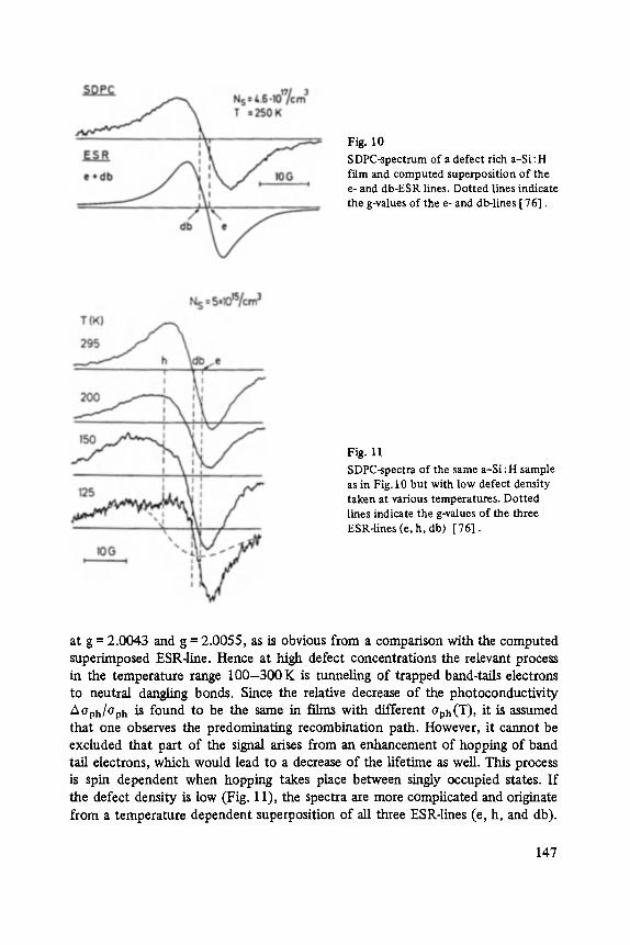
Fig. 10 SDPC-spectrum of a defect rich a-Si : H film and computed superposition of the e- and db-ESR lines. Dotted lines indicate the g-values of the e- and dbqines [76].
Fig. 11 SDPC-spectra of the same a-Si : H sample as in Fig. 10 but with low defect density taken at various temperatures. Dotted lines indicate the g-values of the three ESRqines (e, h, db) [76].
at g = 2.0043 and g = 2.0055, as is obvious from a comparison with the computed superimposed ESR-line. Hence at high defect concentrations the relevant process in the temperature range 1 0 0 - 3 0 0 K is tunneling of trapped band-tails electrons to neutral dangling bonds. Since the relative decrease o f the photoconductivity AOpn/aph is found to be the same in fihm with different aph(T), it is assumed that one observes the predominating recombination path. However, it cannot be excluded that part o f the signal arises from an enhancement of hopping of band tail electrons, which would lead to a decrease of the lifetime as well. This process is spin dependent when hopping takes place between singly occupied states. I f the defect density is low (Fig. 11), the spectra are more complicated and originate from a temperature dependent superposition of all three ESR-lines (e, h, and db).
147
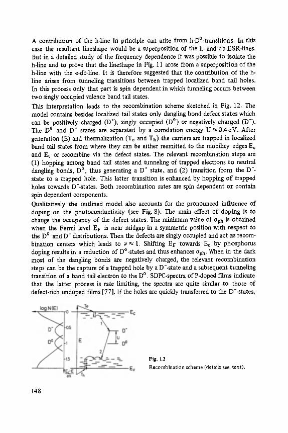
A contribution of the h-line in principle can arise from h-D ~ In this case the resultant lineshape would be a superposition of the h- and db-ESR-lines. But in a detailed study of the frequency dependence it was possible to isolate the Mine and to prove that the lineshape in Fig. 11 arose from a superposition of the h-line with the e-db-line. It is therefore suggested that the contribution of the h- line arises from tunneling transitions between trapped localized band tail holes. In this process only that part is spin dependent in which tunneling occurs between two singly occupied valence band tail states.
This interpretation leads to the recombination scheme sketched in Fig. 12. The model contains besides localized tail states only dangling bond defect states which can be positively charged (D+), singly occupied (D ~ or negatively charged (D-). The D O and D- states are separated by a correlation energy U ~ 0.4eV. After generation (E) and thermalization (Te and Th) the carriers are trapped in localized band tail states from where they can be either reemitted to the mobility edges Ec and Ev or recombine via the defect states. The relevant recombination steps are ( i ) hopping among band tail states and tunneling of trapped electrons to neutral dangling bonds, D ~ thus generating a D- state, and (2) transition from the D-- state to a trapped hole. This latter transition is enhanced by hopping o f trapped holes towards D--states. Both recombination rates are spin dependent or contain spin dependent components.
Qualitatively the outlined model also accounts for the pronounced influence of doping on the photoconductivity (see Fig. 8). The main effect of doping is to change the occupancy of the defect states. The minimum value of O'ph is obtained when the Fermi level EF is near midgap in a symmetric position with respect to the D O and D- distributions. Then the defects are singly occupied and act as recom- bination centers which leads to v ~ 1. Shifting Et: towards Ec by phosphorus doping results in a reduction of D ~ and thus enhances aph. When in the dark most of the dangling bonds are negatively charged, the relevant recombination steps can be the capture of a trapped hole by a D--state and a subsequent tunneling transition of a band tail electron to the D ~ SDPC-spectra of P-doped f'dms indicate that the latter process is rate limiting, the spectra are quite similar to those of defect-rich undoped films [77]. If the holes are quickly transferred to the D--states,
Fig. t2 Recombination scheme (details see text).
148
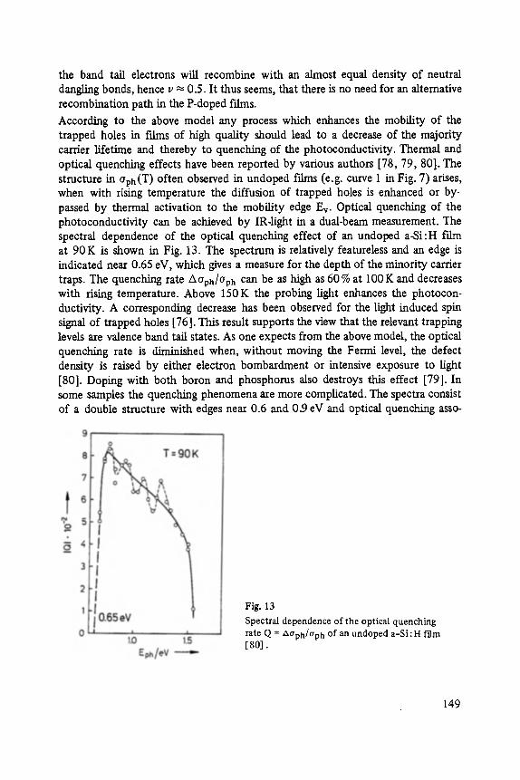
the band tail electrons will recombine with an almost equal density of neutral dangling bonds, hence v ~ 0.5. It thus seems, that there is no need for an alternative recombination path in the P-doped Ftlms.
According to the above model any process which enhances the mobility of the trapped holes in f'rims of high quality should lead to a decrease of the majority carrier lifetime and thereby to quenching of the photoconductivity. Thermal and optical quenching effects have been reported by various authors [78, 79, 80]. The structure in %h(T) often observed in undoped f'rims (e.g. curve 1 in Fig. 7) arises, when with rising temperature the diffusion of trapped holes is enhanced or by- passed by thermal activation to the mobility edge Ev. Optical quenching of the photoconductivity can be achieved by IR-light in a dual-beam measurement. The spectral dependence of the optical quenching effect of an undoped a-Si:H f'tlm at 90K is shown in Fig. 13. The spectrum is reIatively featureless and an edge is indicated near 0.65 eV, which gives a measure for the depth of the minority carrier traps. The quenching rate AOph/Oph Can be as high as 60% at 100K and decreases with rising temperature. Above 150K the probing light enhances the photocon- ductivity. A corresponding decrease has been observed for the light induced spin signal of trapped holes [76]. This result supports the view that the relevant trapping levels are valence band tail states. As one expects from the above model, the optical quenching rate is diminished when, without moving the Fermi level, the defect density is raised by either electron bombardment or intensive exposure to light [80]. Doping with both boron and phosphorus also destroys this effect [79]. In some samples the quenching phenomena are more complicated. The spectra consist of a doubIe structure with edges near 0.6 and 0.9 eV and optical quenching asso-
Fig. 13 Spectral dependence of the optical quenching rate Q = &Oph/erph of an undoped a-Si : H f'flm [80].
149

v~. 14 Plot of (t~r) h versus (/~7) e for undoped (1), boron doped (2) and phosphorus doped (3) a-Si : H-f'tlms. The doping level is indicated unless the doping is uninten- tional [ 81].
ciated with the deeper trap is still observed at 300K [78, 80]. The origin of the deeper trap is to date unclear.
Information on the nature of the states which participate in the recombination processes also comes from time-of-flight experiments. Recently Street e t al. [81] reported on measurements of the/.tr-product by studying the electric field depend- ence of the transient charge collection in a variety of undoped and doped a-Si: H- flims with a thickness 4 - 1 6 / a n and characterized by the spin density Ns (g = 2.0055) of up to 1017 cm -3. The remarkable result shown in Fig. 14 is that the tz~-data can be described by three straight lines which correspond to intrinsic, p-type and n-type samples (curves I, 2, and 3, respectively). For undoped fdms (/~r)e is propor- tional to (~T)h. In these samples neutral dangling bonds act as deep traps for both electrons and holes. This is evident from the observation that the product/~rNs is constant and amounts to 2.5 �9 108 crn -1V -1 for electrons and 4" 1 0 7 c m -1 V -1
for holes. Most remarkably, weak doping with either boron or phosphorus reduces drastically the #r-product of the minority carriers, whereas that of tile majority carriers remains almost unchanged. This behaviour can readily be explained by the generation of charged dangling bond states due to the shift of the Fermi level to either side, which act as effective deep traps for the carrier of opposite charge. These results thus further stress, the important role of the dangling bond defect states for trapping and recombination in a-Si:H and furthermore show that the capture cross section of these defects much depends on their charge state.
Whereas above 100 K the photoconductivity depends sensitively on the kind of preparation, the defect density and the Fermi level position, below 50 K all samples behave quite similarly (Fig. 7). The r~/~r-product becomes independent o f tempera- ture and differs by not more than a factor of 4, although the defect densities in these films differ appreciably, as can be seen from values of the quantum efficiency
150
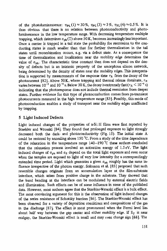
of the photoluminescence: r/pL(1 ) ~ 30%, r/pL(3 ) -~ 3 %, r/pL(4 ) ~ 0.5 %. It is thUS obvious that there is no relation between photoconductivity and photo- luminescence in the low temperature range. With decreasing temperature multiple trapping, which determines %h (T) above 50 K, becomes increasingly less important. Once a carrier is trapped in a tail state the probability for reemission to the con- ducting states is much smaller than that for further thermalization in the tail states until recombination occurs, e.g. via a defect state. As a consequence the time of thermalization and localization near the mobility edge determines the value of Opn. The characteristic time constant then does not depend on the den- sity of defects but is an intrinsic property of the amorphous silicon network, being determined by the density of states near the mobility edges. This interpreta- tion is supported by measurements of the response time rR from the decay of the photocurrent [82]. Above 50 K, where trapping and thermal release dominate, rR varies between 10 -2 and 10 -4 s. Below 30 K, the decay is extremely fast (rR < 10 -6 S) indicating that the photoresponse does not include thermal reemission from deeper states. Further evidence for this type of photoconduction comes from ps-transient photocurrents measured in the high temperature range [83]. Possibly, this mode of photoconduction enables a study of transport near the mobility edges unaffected by trapping.
5 Light Induced Defects
Light induced changes of the properties of a-Si:H ftims were ftrst reported by Staebler and Wronski [84]. They found that prolonged exposure to light strongly decreased both the dark- and photoconductivity (Fig. 15). The initial state A could be restored by annealing above 150 ~ From a study of the time dependence of the relaxation in the temperature range 140-190 ~ these authors concluded that the relaxation process involved an activation energy of 1.5 eV. The light induced changes of %h and od depend on the total light exposure and even occur when the samples are exposed to light of very low intensity for a correspondingly extended time period. Light which generates a given Oph roughly has the same in- fluence irrespective of the photon energy. Solomon et al. [85] proposed that such reversible changes originate from an accumulation layer at the fflm-substrate interface, which arises from positive charge in the substrate. They showed that the band bending at the interface can be modulated by external electric fields and illumination. Such effects can be of some influence in some of the published data. However, most authors agree that the Staebler-Wronski effect is a bulk effect. The most convincing argument for this is the observation of light induced changes of the series resistance of Schottky barriers [86]. The Staebler-Wronski effect has been observed for a variety of deposition conditions and compositions of the gas in the discharge [87]. The effect is most pronounced when the Fermi level lies about half way between the gap center and either mobility edge. If EF is near midgap, the Staebler-Wronski effect is small and may even change sign [88]. The
151
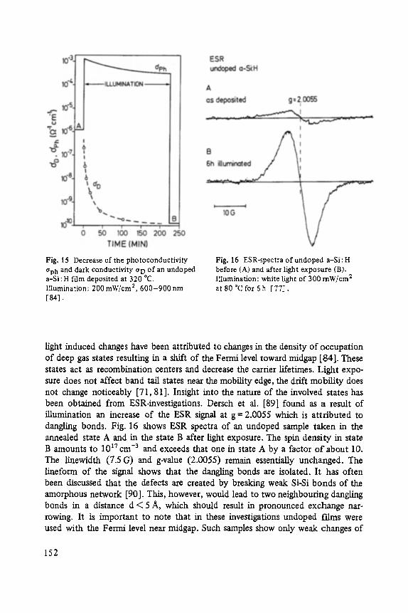
Fig. 15 Decrease of the photoconductivity apb and dark conductivity (7 D of an undoped a-Si:H film deposited at 320 ~ Illumination: 200 mW/cm 2, 600-900 nm [~ ] .
Fig. 16 ESR-spectra of undoped a-Si : H before (A) and after light exposure (B). Illumination: white light of 300 rnW/cm 2 at 80 ~ for 6h [773.
light induced changes have been attributed to changes in the density of occupation of deep gas states resulting in a shift of the Fermi level toward midgap [84]. These states act as recombination centers and decrease the cartier lifetimes. Light expo- sure does not affect band tail states near the mobility edge, the drift mobility does not change noticeably [71, 81]. Insight into the nature of the involved states has been obtained from ESR-investigations. Dersch et al. [89] found as a result of illumination an increase of the ESR signal at g = 2.0055 which is attributed to dangling bonds. Fig. 16 shows ESR spectra of an undoped sample taken in the annealed state A and in the state B after light exposure. The spin density in state B amounts to 1017 cm -3 and exceeds that one in state A by a factor o f about 10. The linewidth (7.5 G) and g-value (2.0055) remain essentially unchanged. The lineform of the signal shows that the dangling bonds are isolated. It has often been discussed that the defects are created by breaking weak Si-Si bonds of the amorphous network [90]. This, however, would lead to two neighbouring dangling bonds in a distance d ( 5 A, which should result in pronounced exchange nar- rowing. It is important to note that in these investigations undoped films were used with the Fermi level near midgap. Such samples show only weak changes of
152
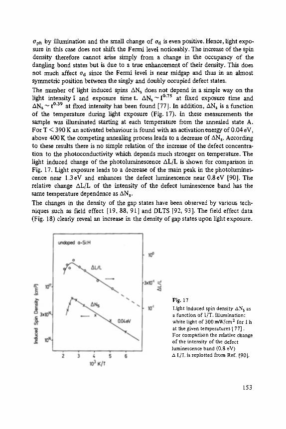
Oph by illumination and the small change of Od is even positive. Hence, light expo- sure in this case does not shift the Fermi level noticeably. The increase of the spin density therefore cannot arise simply from a change in the occupancy of the dangling bond states but is due to a true enhancement of their density. This does not much affect Od since the Fermi level is near midgap and thus in an almost symmetric position between the singly and doubly occupied defect states.
The number of light induced spins ANs does not depend in a simple way on the light intensity I and exposure time t. ANs~ 10.75 at fixed exposure time and ANs "" t ~ at f r e d intensity has been found [77]. In addition, ANs is a function of the temperature during light exposure (Fig. 17). In these measurements the sample was illuminated starting at each temperature from the annealed state A. For T < 390 K an activated behaviour is found with an activation energy of 0.04 eV, above 400 K the competing annealing process leads to a decrease of ANs. According to these results there is no simple relation of the increase of the defect concentra- tion to the photoconductivity which depends much stronger on temperature. The light induced change of the photoluminescence AL/L is shown for comparison in Fig. 17. Light exposure leads to a decrease of the main peak in the photolumines- cence near 1.3 eV and enhances the defect luminescence near 0.8 eV [90]. The relative change AL/L of the intensity of the defect luminescence band has the same temperature dependence as ANs.
The changes in the density of the gap states have been observed by various tech- niques such as field effect [19, 88, 9 t ] and DLTS [92, 93]. The field effect data (Fig. 18) clearly reveal an increase in the density of gap states upon light exposure.
Fig. 17 Light induced spin density AN s as a function of 1/T. Illumination: white light of 300 mW/cm 2 for 1 h at the given temperatures [ 77]. For comparison the relative change of the intensity of the defect luminescence band (0.8 eV) A L/L is replotted from Ref. [901.
153
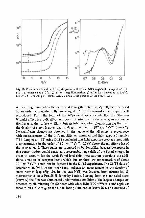
Fig. 18 Current as a function of the gate potential (left) and N(E) (right) of undoped a-Si: H [19]. (1)annealed at 170 ~ (2) after strong illumination, (3) after 0.5 h annealing at 170~ (4) after 4 h annealing at 170 ~ Arrows indicate the position of the Fermi level.
After strong illumination the current at zero gate potential, V~- = 0, has decreased by an order of magnitude. By annealing at 170 ~ the original curve is quite weU reproduced. From the form of the I-VF-Curves we conclude that the Staebler- Wronski effect is a bulk effect and does not arise from a decrease of an accumula- tion layer at the surface or f'flm-substrate interface. After illumination we find that the density of states is raised near midgap to as much as 10 is cm -3 eV -1 (curve 2). No significant changes are observed in the region of the tail states in accordance with measurements of the drift mobility on annealed and light exposed samples [71]. Lang et al. [92] using DLTS concluded that light exposure creates states with a concentration in the order of 10 Is cm -3 eV -~, 0.5 eV above the mobili ty edge of the valence band. These states are supposed to be donorlike, because acceptors in this concentration would cause an unreasonably large shift of the Fermi energy. In order to account for the weak Fermi level shift these authors postulate the addi- tional creation o f acceptor levels which due to their low concentration of about 1016 cm -3 eV -1 could not be detected in the DLTS-experiment. The DLTS-data of Beichler et al. [93], on the other hand, indicate an enhancement of the density of states near midgap (Fig. 19). In this case N(E) was deduced from current-DLTS- measurements on a Pt/a-Si:H Schottky barrier. Starting from the annealed state (curve A) the f'tim was illuminated under various conditions. The largest changes are observed by illuminating for 60 hours with white light (500 mW/cm 2) and applying forward bias, V > Voc, to the diode during illumination (curve B3). The increase of
154
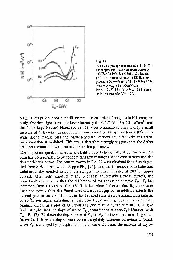
Fig. 19 N(E) of a phosphorus doped a-Si : H film (100 ppm PH3) derived from current- DLTS of a Pt/a-Si:H Schottky barrier [93] (A) annealed state; (B3) light ex- posure 500 mW/cm 2 of 1-3 eV for 60 h, bias V > Voc; (B1) 50 mW]cm 2, hv < 1.7 eV, 15 h, V > Voc; (B2) same as B1 except bias V = - 2 V.
N (E) is less pronounced but still amounts to an order of magnitude if homogene- ously absorbed light is used of lower intensity (hv < 1.7 eV, 15 h, 50 mW/cm ~) and the diode kept forward biased (curve B1). Most remarkably, there is only a small increase of N(E) when during illumination reverse bias is applied (curve B2). Since with strong reverse bias the photogenerated carriers are effectively extracted, recombination is inhibited. This result therefore strongly suggests that the defect creation is connected with the recombination processes.
The important question whether the light induced changes also affect the transport path has been adressed to by concomitant investigations of the conductivity and the thermoelectric power. The results shown in Fig. 20 were obtained for a trim depos- ited from Sill4 doped with 100ppmPH3 [94]. In order to remove adsorbates and unintentionally created defects the sample was f~rst annealed at 280 ~ (upper curves). After light exposure a and S change appreciably (lowest curves), the remarkable result being that the difference of the activation energies E ~ - Es has increased from 0.09eV to 0.21eV. This behaviour indicates that light exposure does not merely shift the Fermi level towards midgap but in addition affects the current path in the a-Si: H t-tim. The light soaked state is stable against annealing up to 80 ~ For higher annealing temperatures T A, o and S gradually approach their original values. In a plot of Q versus I /T (see relation 6) the data in Fig. 20 give fairly straight lines the slope of which EQ, according to relation 7, is identical with E o - E s. Fig. 21 shows the dependence of EQ on Ea for the various annealing states (curve 1). It is interesting to note that a completely different behaviour is found, when Eo is changed by phosphorus doping (curve 2). Thus, the increase of EQ by
155
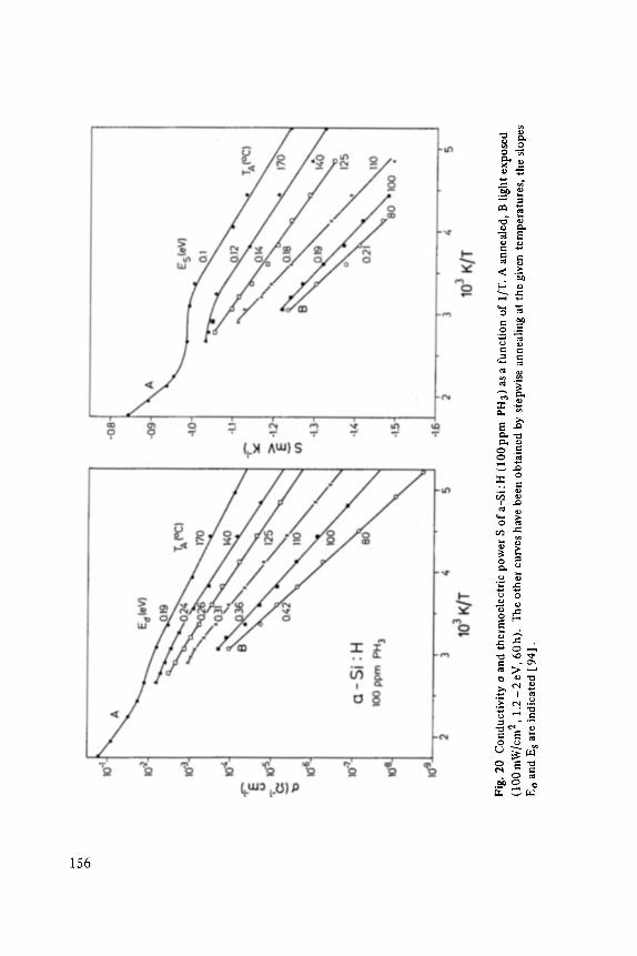
156
e.. e..
o.q
e - l . ~
g~ E ~ .
~ o
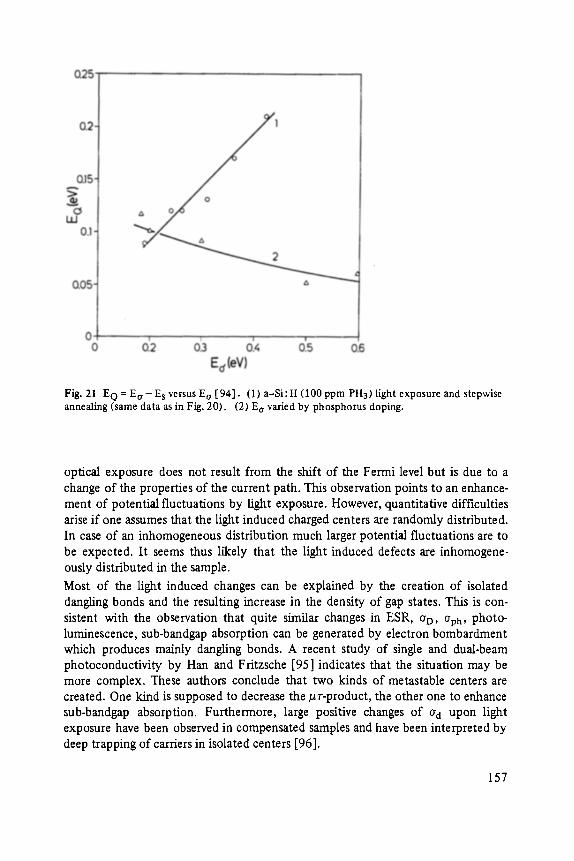
Fig. 21 EQ = E o - E s versus E o [ 94]. (1) a-Si: H (100 ppm PH3) light exposure and stepwise annealing (same data as in Fig. 20), (2) E o varied by phosphorus doping.
optical exposure does not result from the shift of the Fermi level but is due to a change of the properties of the current path. This observation points to an enhance- ment of potential fluctuations by light exposure. However, quantitative difficulties arise if one assumes that the light induced charged centers are randomly distributed. In case of an inhomogeneous distribution much larger potential fluctuations are to be expected. It seems thus likely that the light induced defects are inhomogene- ously distributed in the sample.
Most of the light induced changes can be explained by the creation of isolated dangling bonds and the resulting increase in the density of gap states. This is con- sistent with the observation that quite similar changes in ESR, a D, aph, photo- luminescence, sub-bandgap absorption can be generated by electron bombardment which produces mainly dangling bonds. A recent study of single and dual-beam photoconductivity by Han and Fritzsche [95] indicates that the situation may be more complex. These authors conclude that two kinds of metastable centers are created. One kind is supposed to decrease the #r-product, the other one to enhance sub-bandgap absorption. Furthermore, large positive changes of a a upon light exposure have been observed in compensated samples and have been interpreted by deep trapping of carriers in isolated centers [96].
157
The mechanism for defect creation is still quite unclear. Different models have been put forward to explain these effects which in part consider the role of impurities like oxygen [87]. Staebler and Wronski [84] assumed that the energy released during recombination may be sufficient to cause local rearrangements of bonds possibly involving hydrogen. Similarly, Dersch et al. [89] proposed that weak Si-Si bonds are broken and that the surrounding network relaxes leading to a somewhat larger distance of the involved Si-atoms. From neighbouring Si-H bonds hydrogen atoms are believed to switch to the arising bonds leaving behind an isolated dangling bond. By continuous exchange of hydrogen atoms the dangling bonds are supposed to move further apart and to stabilize. This model needs extended clusters of Si-H bonds. Proton magnetic resonance studies in fact indicate that the distribution of hydrogen is inhomogeneous in glow discharge a-Si-samples [11], and the enhance- ment of the potential fluctuations suggests an inhomogeneous distribution of the light induced defects. However, there is to date no direct proof for the participation of hydrogen. In particular there is no proof for a correlation of the Staebler- Wronski~ffect with the hydrogen contents of the f'rims. Possibly hydrogen is not directly involved, but plays a more indirect role determining the structure of the amorphous silicon network. It may depend on the solution of this problem whether amorphous silicon deposited from the glow discharge can successfully be used for fabricating optoelectronic devices like solar cells.
References
[1] vr E. Spear, Amorphous and Liquid Semiconductors, edits. J. Stuke and W. Brenig (Taylor & Francis, London 1974) p. 1
[21 T.D. Moustakas, I. Electron. Materials 8,391 (1979) [31 W. Paul D. A. Anderson, Solar Energy Mat. 5,229 (1981) 141 D. Kaplan, iV. SoL G. Velasco, P.A. Thomas, Appl. Phys. Lett. 35, 44 (1978) I51 N. Sol, D. Kaplan, D. Dieurnegard, D. Dubreuil, J. Non-Cryst. Solids 35/36,291 (1980) [61 B.A. Scott, in: Amorphous Hydrogenated Silicon, ed. J.I. Pankove (Academic Press,
1984) [7] M. Milleville, W. Fuhs, F.J. Demond, H. Mannsberger, G. Maller, S. Kalbitzer, Appl.
Phys. Lett. 34, 173 (1979) 18] W. Beyer, H. Wagner, J. Non-Cryst. Solids 59/60, 161 (1983) {91 G. Lucovsky, R. Z Nemanich, J. C. Knights, Phys. Rev. BI9, 2064 (1979)
[101 J.C. Knights, J. Non-Cryst. Solids 35/36,159 (1980) [111 J.A. Reimer, R. W. Vaughan, J. C. Knights, Phys. Rev. Lett. 44, 193 (1980) [12] ~r E. Spear, P. G. LeComber, Sohd State Comm. 17, 1193 (1975) [13] D.C. Carlson, C.R. ICronski, Appl. Phys. Lett. 28,671 (1976) [14] D. Carlson, Solar Energy Mat. 3, 106 (1980) [15] H. Fritzsche, Solar Energy Mat. 3,447 (1980)
158
[16] Amorphous Hydrogenated Silicon, ed. J. L Pankove (Academic Press 1984). The Physics of Amorphous Silicon and its Applications, ed. J. D. Joannopoulos, G. Lucovsky (Springer, Berlin 1984)
[171 A. Madan, P. G. LeComber, IV. E. Spear, J. Non-Cryst. Solids 20,239 (1976) [18] N.B. Goodman, H. Fritzsche, Phil. Mag. B42, 149 (1980) [191 K. iveber, M. G~newaM, iv. Fuhs, P. Thomas, phys. stat. soi.(b) llO, 133(1982)
[20] D. V. Lang, J. D. Cohen, J. P. Harbison, Phys. Rev. B25, 5285 (1982)
[211 J. Beichler, H. MeU, K. Weber, J. Non-Cryst. Solids 59/60, 257 (1983) [22] R.A. Street, D. K. Biegelsen, Solid State Comm. 33, 1159 (1980) [231 R.A. Street, J. C. Knights, D. K. Biegelsen, Phys. Rev. BI8, 1880 (1978) [241 U. Voget-Grote, IV. Kiimmerle, R. Fischer, J. Stuke, Phil. Mag. B41,127 (1980) [251 H. Dersch, J. Stuke, J. Beichler, phys. st.at, sol. (b) 105,265 (1981) [26] H. Dersch, J. Stuke, Z Beichler, phys. stat. sol. (b) 107, 307 (1981) [271 N.F. Mott, E.A. Davis, Electronic Processes in Non-Crystalline Materials (Clarendon
Press, Oxford, 1979) [28] M.H. Cohen, E. N. Economou, C. M. Soukoulis, Phys. Rev. Lett. 51, 1202 (1983) [291 H. Mueller, P. Thomas, Phys. Rev. Lett. 51,702 (1983) [301 P. G. LeComber, D. ,I. Jones, IV. E. Spear, Phil. Mag. 35, 1173 (1977) [31] M. Roilox, Phil. Mag. B38,477 (1978) [321 N.F. Mott, Adv. Physics 16, 49 (1967) [331 H. Overhof, IV. Beyer, Phil. Mag. B47,377 (1983) [34] W. Beyer, 1"1. Overhof, in: Electronic and Transport Properties of Hydrogenated Amor-
phous Silicon, ed. Z L Pankove (Academic Press, 1984)
[35 ] N.F. Mott, Phil. Mag. 19,835 (1969) [361 J. C. Knightx, T.M. Hayes, J. C. Mikkelsen, Phys. Rev. Lett. 39, 712 (1977)
[371 IV. E. Spear, P. G. LeComber, Phil. Mag. 33,935 (1976) [381 R.A. Street, D. K. Biegelsen, Z C. Knights, Phys. Rev. B24,969 (1981) [391 J. C. Zesch, R. A. Lu]an, V. R. Deline, J. Non-Cryst. Solids 35/36,273 (1980) [401 IV. Beyer, H. Mell, H. Overhof, in: Amorphous and Liquid Semiconductors, edit. IV. E.
Spear (CICL, Edinburgh 1977) p. 328 [411 IV. Beyer, H. Mell, in: Amorphous and Liquid Semiconductors, edit. IV. E. Spear (CICL,
Edinburgh 1977) p. 333 [42] Z.S. Jan, R. H. Bube, J. C. Knights, J. Electron Mat. 8, 47 (1979); J. Appl. Phys. 51,
3378 (1980) [431 C. C. TsaL H. Fritzsche, H. Tanielian, M. H. Gaczi, P. D. Persans, M. A. l/asaghi, in:
Amorphous and Liquid Semiconductors, edit. IV. E. Spear (CICL, Edinburgh 1977) p. 339
[441 IV. Beyer, H. Mell, H. Overhof, J. Physique 42, C4-104 (1981) [451 S. Kalbitzer, G. Miiller, P. G. LeComber, IV. E. Spear, Phil. Mag. B41,439 (1980)
[46] IV. Beyer, R. Fischer, 1-1. Overhof, Phil. Mag. B39,205 (1979) 147] IV. Beyer, R. Fischer, H. Wagner, J. Electron. Mat. 8, 127 (1979) [48] IV. E. Spear, D. Allen, P. G. LeComber, A. Ghaith, J. Non-Cryst. Solids 35/36, 357 (1980)
[491 L. Ley, in: Physics of Amorphous Silicon and its Application, edits. J. D. Joannopoulos, G. Lucovsky (Springer, Berlin, 1984)
159
[50l D. 3". Jones, P. G. LeComber, W.E. Spear, Phil. Mag. 36,541 (1977) [51] P. G. LeComber, W.E. Spear, D. Allen, J. Non-Cryst. Solids 32, 1 (1979) [52] W. Beyer, It. Overho[, Solid State Comm. 31, 1 (1979)
[531 H. Overhof, W. Beyer, Phil. Mag. B43, 433 (1980) [54] H. Fritzsche, J. Non-Cryst. Solids 6, 49 (1971) [55] G. D6hler, Phys. Rev. BI9, 2083 (1979) [56] W.B. Jackson, N. M. Amer, Phys. Rev. B25, 5559 (1982) [57] K. Tanaka, S. Yamasaki, Solar Energy Mat. 8, 277 (1982) [58] C.R. Wronski, B. Abeles, 7". Tied~e, G.D. Cody, Solid State Comm. 44, 1423 (1982)
[59] R.A. Street, Phys. Rev. Lett. 49, 1187 (1982) [60] R.A. Street, D. K. Biegelsen, J. C. Knights, Phys. Rev. B24, 969 (1981)
[61 ] R. Fischer, in: Amorphous Semiconductors, Topics in Appl. Phys. 36, ed. M. H. Brodsky (Springer, New York, 1979) p. 159
[62] R.A. Street, Adv. in Physics 30,593 (I981) [63] M. Hoheisel, R. Carius, W. Fuhs, J. Non-Cryst. Solids 59/60, 457 (1983)
[64l D.A. Anderson, W.E. Spear, Phil. Mag. B36,695 (1977) [65] R. Fischer, W. Rehm, J. Stuke, U. Voget-Grote, J. Non-Cryst. Solids 35/36,687 (1980)
[66] A.R. Moore, Appl. Phys. Lett. 31,762 (1977) [67] W.E. Spear, L Non-Cryst. Solids 59/60, 1 (1983) [68] M. Hoheisel, W. Fuhs, to be published [69] W.E. Spear, R. J. Loveland, A. AISharbaty, J. Non-Cryst. Solids 15,410 (1974) [70] Ir E. Spear and P. G. LeComber, in: Photoeonductivity and Related Phenomena, edits.
J. Mort and D. M. Pai (Elsevier, New York 1976) p. 213 [71] W. Fuhs, M. Milleville, J. Stuke, phys. star. sol. (b) 89,495 (1978)
[72] C.R. Wronski, R. E. Daniel, Phys. Rev. B23, 794 (1981) [73] H. Mell, B. Movaghar, L. Schweitzer, phys. star. sol. (b) 88, 531 (1978) [74] R.A. Street, D. K. Biegelsen, J. C. Knights, C. Tsang, R.M. White, Solid State Electron.
21, 1461 (1978) [75] K. Morigaki, Y. Sano, J. Hirabayashi, Solid State Comm. 39,947 (1981) [76] H. Dersch, L. Schweitzer, J. Stuke, Phys. Rev. B28, 4678 (1983) [77] H. Dersch, Dissertation, Universit~t Marburg (1983) [781 J.P. Persans, Phil. Mag. B46,435 (1982) [79] P.E. Vanier, R. W. Griffith, LAppl . Pliys. 53,3098(1982)
[801 W. Fuhs, H.M. Welsch, D.C. Booth, phys. stat. sol.(b) 120,197(1983)
[81 ] R.A. Street, J. Zesch, M. J. Thompson, Appl. Phys. Lett. 43, 672 (1983)
[82] M. Hoheisel, R. Carius, W. Fuhs, J. Non-Cryst. Solids (1984) in press [83] A.M. Johnson, D.H. Auston, P.R. Smith, J.C. Beans, J.P. Harbison, A.C:Adams, Phys.
Rev. B23, 6816 (1981)
[841 D.L. Staebler, C.R. Wronski, Appl. Phys. Lett. 31,292 (1977); J. Appl. Phys. 51, 3262 (1980)
[85 ] I. Solomon, T. Died, D. Kaplan, J. de Physique 39, 1241 (1978)
[86] D.E. Carlson, C.R. Wronski, in: Amorphous Semiconductors, Topics in Appl. Physics 36, ed. M. H. Brodsky (Springer, New York 1979) p. 287
160
[87] D.E. Carlson, Solar Energy Mat. 8, 129 (1982) I881 M.H. Tanielian, N. B. Goodman, H. Fritzsche, J. de Physique 42, C4-375 (1981) 189] H. Dersch, J. Stuke, J. Beichler, Appl. Phys. Lett. 38,456 (1981)
I901 J.I. Pankove, J. E. Berkeyheiser, Appl. Phys. Lett. 37,705 (1980) 191] M.J. Powell, B. C. Easton, D. H. Nicholls, J. de Physique 42, C4-379 (1981) [921 D. V. Lang, J. D. Cohen, J. P. Harbison, A. M. Sergent, Appl. Phys. Lett. 40, 474 (1982) [931 J. Beichler, H. Mell, Proc. 4 th Photovoltaic Solar Energy Conf., Stresa 1982, p. 537
[941 D. Hauschildt, W. Fuhs, H. Mell, phys. star. sol. (b) 111,171 (1982) [95] D. Han, H. Fritzsche, J. Non-Cryst. Solids 59/60, 397 (1983)
[961 H. Mell, ~r Beyer, J. Non-Cryst. Solids 59/60,405 (1983)
161
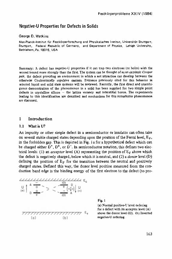
Festk6rperprobleme X X l V (1984)
Negative-U Properties for Defects in Solids
George D. Watkins
Max-Planck-lnstitut f(Jr Festk6rperforschung and Physikalisches Institut, Universit~it Stuttgart, Stuttgart, Federal Republic of Germany, and Department of Physics, Lehigh University, Bethlehem, Pa. 18015, USA
Summary: A defect has negative-U properties if it can trap two electrons (or holes) with the second bound more strongly than the first. The system can be thought of as an extrinsic Cooper pair, the defect providing an environment in which a net attraction can develop between the otherwise Coulombically repulsive carriers. Evidence previously cited for this behavior in selected liquid and solid state systems will be reviewed. Recently, the first direct and unambi- guous demonstration of the phenomenon in a solid has been supplied for two simple point defects in crystalline silicon - the lattice vacancy and interstitial boron. The experiments leading to this identification are described and mechanisms for this remarkable phenomenon ate discussed.
1 I n t r o d u c t i o n
1.1 What is U?
An impurity or other sirnple defect in a semiconductor or insulator can often take on several stable charged states depending upon the position of the Fermi level, EF, in the forbidden gap. This is depicted in Fig. 1 a for a hypothetical defect which can be charged either D +, D ~ or D-. In semiconductor notation, this defines two elec- trical levels: (1) an acceptor level (A) representing the position of E F above which
the defect is negatively charged, below which it is neutral, and (2) a donor level (D) defining the position of E F for the transition between the neutral and positively charged states. Defined this way, the donor level position measured from the con- duction band edge is the binding energy of the first electron to the defect (to pro-
Fig. l (a) Normal positive-U level ordering for a defect with its acceptor level (A) above the donor level (D). (b) Inverted negative-U ordering.
163

duce the neutral state) and the acceptor level position, again measured from the conduction band edge, is the binding energy of a second electron to produce the negatively charged state. The acceptor level is expected to be above the donor level because the second electron is repelled by the Coulomb interaction with the first electron. This added Coulomb repulsion energy is defined as U and in Fig. 1 a is the separation between the donor and acceptor levels. U is often called the Hubbard "correlation energy" being first introduced by Hubbard in his treatment of con- ductivity in narrow band semiconductors [ 1 ].
For an atom or ion in free space, U is therefore simply the difference between the ionization energy and the electron affinity (the binding energy of a second electron). In this case, U is typically of the order of several electron volts. For example, for the neutral boron atom B ~ the ionization energy is 8.3 eV, the electron afl'mity 0.28 eV, giving U ~ 8 eV. For the In 2§ ion, U ~ 9 eV. However, when an atom or ion is dissolved as an impurity into a solid, the correlation energies can be greatly reduced. This is in part because of the dielectric shielding of the Coulomb interac- tions and from charge delocalization effects due to hybridization with band states of the solid via strong wavefunction overlap with its neighbors, etc. Typical values of U for impurities in silicon, for instance, are only ~ 0.2-0.3 eV, often still allowing therefore several charged states for an impurity or defect within its narrow band gap (-~ 1 eV).
1.2 Positive-U
Until relatively recently, all defects which introduce more than one level into a semiconductor were either known to have normal positive-U behavior or were assumed to have this property, on the reasonable assumption that electron-electron interactions are repulsive. For the example of Fig. la, for instance, the normal positive-U ordering of levels means that each of the three charge states o f the de- fect D +, D ~ D-, can be thermodynamically stable depending upon the position of the Fermi level, E F. The donor and acceptor levels have unambiguous meanings and can be measured directly either by Hall measurements (Fermi level position under thermodynamic equilibrium conditions of capture and emission of carriers at each level) or by direct ionization excitation from the levels to the conduction and valence band edges.
1.3 Negative-U
Negative-U properties for a defect mean that the levels are inverted from their usual order, with the acceptor level below the donor level, as shown in Fig. lb . Let us defer for the moment how this might come about, or if it is possible at all, and con- sider the unusual properties that such a defect would have.
164
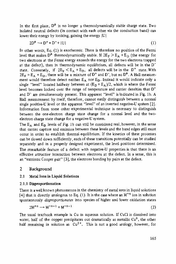
In the first place, D O is no longer a thermodynamically stable charge state. Two isolated neutral defects (in contact with each other via the conduction band) can lower their energy by ionizing, gaining the energy IUI
2D ~ ---* D+ + D-+ IUI ( i )
In other words, Eq. (1) is exothermic. There is therefore no position of the Fermi level that makes D O thermodynamically stable. If 2EF > E A + EI~ (the energy for two electrons at the Fermi energy exceeds the energy for the two electrons trapped at the defect), then in thermodynamic equilibrium, all defects will be in the D- state. Conversely, if 2EF < EA + ED, all defects will be in the D § state. With 2E F = E A + ED, there will be a mixture o fD § and D-, but no D ~ A Hall measure- ment would therefore detect neither EA nor ED. Instead it would indicate only a single "level" located halfway between at (ED + EA)/2, which is where the Fermi level becomes locked over the range of temperature and carrier densities that D § and D- are simultaneously present. This apparent "level" is indicated in Fig. lb. A Hall measurement by itself, therefore, cannot easily distinguish between a normal single positive-U level or the apparent "level" of an inverted negative-U system [2]. Information from some other experimental technique is necessary to distinguish between the one-electron charge state change for a normal level and the two- electron charge state change for a negative-U system.
The E A and ED levels of Fig. lb can still be considered real, however, in the sense that carrier capture and emission between these levels and the band edges still must occur in order to establish thermal equilibrium. If the kinetics of these processes can be slowed down sufficiently, each of these transitions potentially can be studied separately and in a properly designed experiment, the level positions determined.
The remarkable feature of a defect with negative-U properties is that there is an effective attractive interaction between electrons at the defect. In a sense, this is an "extrinsic Cooper pair" [3], the electrons bonding by pairs at the defect.
2 B a c k g r o u n d
2.1 Metal Ions in Liquid Solutions
2.1.1 Disproportionation
There is a well known phenomenon in the chemistry of metal ions in liquid solutions [4] that is directly analogous to Eq. (1). It is the case where an M +n ion in solution spontaneously disproportionates into species of higher and lower oxidation states
2M *n ~ M "rn'l + M *n-1 (2)
The usual textbook example is Cu in aqueous solution. If CuC1 is dissolved into water, half of the copper precipitates out dramatically as metallic Cu ~ the other half remaining in solution as Cu 2 +. This is not a good analogy, however, for
165
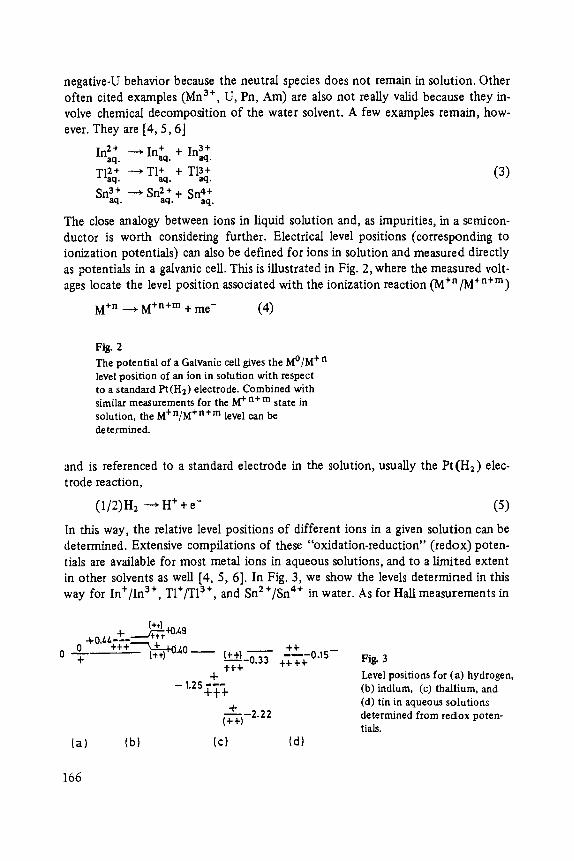
negative-U behavior because the neutral species does not remain in solution. Other often cited examples (Mn 3+, U, Pn, Am) are also not really valid because they in- volve chemical decomposition o f the water solvent. A few examples remain, how- ever. They are [4, 5, 6]
In2aq " ~ In+q + 1-3+ �9 ILaq.
T12+. --+ Tl+aq. + Tla+aq. (3)
Sn 3+ ~ Sn z+ + Sn 4+ aq. aq. aq.
The close analogy between ions in liquid solution and, as impurities, in a semicon- ductor is worth considering further. Electrical level positions (corresponding to ionization potentials) can also be defined for ions in solution and measured directly as potentials in a galvanic cell. This is illustrated in Fig. 2, where the measured volt- ages locate the level position associated with the ionization reaction (M+n/M +n+m)
M +n ~ M +n+m + me- (4)
Fig. 2
The potential of a Galvanic cell gives the M~ +n level position of an ion in solution with respect to a standard Pt(H2) electrode�9 Combined with similar measurements for the M +n+m state in solution, the M+n/M +n+m level can be determined.
and is referenced to a standard electrode in the solution, usually the Pt(H2) elec- trode reaction,
(1/2)H2 --> H + + e- (5)
In this way, the relative level positions of different ions in a given solution can be determined. Extensive compilations of these "oxidation-reduction" (redox) poten- tials are available for most metal ions in aqueous solutions, and to a limited extent in other solvents as well [4, 5, 6]. In Fig. 3, we show the levels determined in this way for In+/In 3+, TI+/T13§ and Sn2+/Sn 4+ in water. As for HaU measurements in
~ - I . o 49 q- __...j§247 �9 0 " + + + " - ' ~ ~" I.OAO ++ + (-F+) {++)-0.33 -~ -0 .15- - Fig. 3
-i- ,i- -i- 4- Level positions for (a) hydrogen,
- 1.25 ~_~. (b) indium, (c) thallium, and (d) tin in aqueous solutions
+ - 2 . 2 2 determined from redox poten- (§247 tiats.
(a) (b) (c) (d)
166

semiconductors, these potential measurements are under thermodynamic equilibrium conditions and only a single "level" is normally detected separating the two stable charge states. In the case of In and T1, however, the lifetimes of the metastable (2+) states were long enough to allow an estimate of the single charge state change levels. These are also given in the figure and demonstrate unambiguous negative-U be- havior in these two cases.
2.1.2 Alkali metals in liquid ammonia
Solutions of alkali metals in liquid NH3 display unusual properties that have in- trigued chemists and physicists for well over a century [7, 8]. Already in the mid- 1940's, it was recognized that there was something happening that was akin to negative-U behavior. At very low concentrations, it was deduced that sodium dissolved into solution as
Na ~ ~ Na § + e-sol (6)
where the solvated electron e~o I was actually inside of a bubble in the liquid (~ 4 NH3 molecules in volume) [9]. Upon increasing the sodium content, however, the color of the solution changed [ 10], photoconductivity properties changed [11 ], and the paramagnetism of the solvated electrons diminished [ 12]. From this it was suggested that there was a net attraction between two solvated electrons
2%ol ~ ( e - . e-)sol + ~ 0.2 eV (7)
the electrons pairing diamagnetically in a single bubble [9] with a net binding energy (negative-U) of ~- 0.2 eV [ 13]. This interpretation implies negative-U as an intrinsic property of the NH3 solvent (occurs independently of how the electrons are in- troduced). We will see in a later section that this bears a close resemblance to bipolarons, recently suggested for intrinsic negative-U behavior in some semicon- ductors.
At the present time, however, it appears to be more generally believed that the pairing of the electrons requires the simultaneous presence of a Na + ion to over- come their Coulomb repulsion. Calculations have not been able to confirm attrac- tive interaction between the two solvated electrons alone [14, 15]. This modern interpretation, therefore, also becomes equivalent to disproportionation of Na ~
2 Na~ ~ Na+ + (%o1" Na+" esol) (8)
where the (e~ol �9 Na + �9 e~ol) complex is equivalent to Na-. It is the sodium impurity therefore that has the negative-U property in the NH 3 solvent.
So far there has been no direct proof of this in liquid NH3. However, evidence has been presented for the disproportionation of Na ~ into Na + and Na- in closely re- lated organic solvents (methamine, ethylamine, tetrahydrofuran) [16]. By adding crown or cryptand ethers to the solvent to enhance the metal solubility and to complex the Na § ion to prevent rapid Na + exchange, two sharp equally intense
167
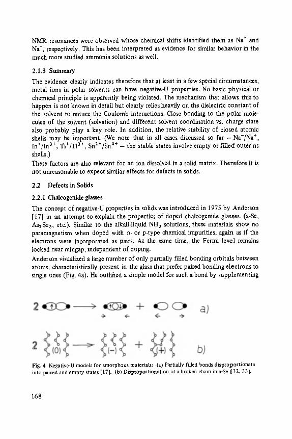
NMR resonances were observed whose chemical shifts identified them as Na + and Na-, respectively. This has been interpreted as evidence for similar behavior in the much more studied ammonia solutions as well.
2.1.3 Summary
The evidence clearly indicates therefore that at least in a few special circumstances, metal ions in polar solvents can have negative-U properties. No basic physical or chemical principle is apparently being violated. The mechanism that allows this to happen is not known in detail but clearly relies heavily on the dielectric constant of the solvent to reduce the Coulomb interactions. Close bonding to the polar mole- cules of the solvent (solvation) and different solvent coordination vs. charge state also probably play a key role. In addition, the relative stability of closed atomic shells may be important. (We note that in all cases discussed so f a r , - N a - / N a +, In+/In 3+, TI+/TI 3+, sna+/sn 4+ - the stable states involve empty or filled outer ns shells.)
These factors are also relevant for an ion dissolved in a solid matrix. Therefore it is not unreasonable to expect similar effects for defects in solids.
2.2 Defects in Solids
2.2.1 Chalcogenide glasses
The concept of negative-U properties in solids was introduced in 1975 by Anderson [ 17] in an attempt to explain the properties of doped chalcogenide glasses. (a-Se, AsaSe3, etc.). Similar to the alkali-liquid NH3 solutions, these materials show no paramagnetism when doped with n- or p-type chemical impurities, again as if the electrons were incorporated as pairs. At the same time, the Fermi level remains locked near midgap, independent of doping.
Anderson visualized a large number of only partially filled bonding orbitals between atoms, characteristically present in the glass that prefer paired bonding electrons to single ones (Fig. 4a). He outlined a simple model for such a bond by supplementing
Fig. 4 Negative-U models for amorphous materials: (a) Partially filled bonds disproportionate into paired and empty states [17 ]. (b) Disproportionation at a broken chain in a-Se [ 32, 33 I-
168
the normal Hubbard Hamiltonian with a linear electronic coupling to the displace- ment (x) between the two atoms and a quadratic elastic restoring term
V = - Lx(nt + n~) + (1/2)cx 2 (9)
where nt and n~ are the occupancies (0 or 1) of the spin-up and spin-down bond orbitals, respectively. Taking ~2V/ax2 = 0, the energy for single occupancy is there- fore lowered by - X 2/2c as the atoms relax toward each other, and the energy for double occupancy by -2~,2]c, as they relax further together. Adding the normal Hubbard correlation energy U, the net effective correlation energy, defined by the energy difference between two singly occupied bonds (2Xt) and the dispropor- tionated state (X0 + X2), becomes
U~r = U - ?,2/c (10)
For sufficiently large X2/c, the correlation energy could therefore become negative. The pinning of E F would naturally occur at the X2/X0 "level", associated with partial occupancy of these two states, so long as the concentration of these available partially filled bonds exceeds the dopant concentration.
Anderson's model did not envision defects. Rather, as he pointed out, it is essentially a model of bipolarons, intrinsic to the glassy material, where the polaronic lattice relaxation energy of two electrons together overcomes their Coulomb repulsion, providing a lower energy state than the two separated polarons*. It therefore bears a formal similarity to the earlier models for the alkali-liquid NH3 behavior, Eq. (7), the "polaronic" character of the solvated electron being the bubble and the "bi- polaronic" character, the two electrons sharing a common bubble.
The basic ideas of Anderson were later adapted by Street and Mort [32] to defects in the material where constraints in the local topography provide atoms with dangl- ing bonds. Kastner, Adler, and Fritzsche [33] subsequently suggested several specific defect configurations which might have these negative-U properties, labeling them valence alternation pairs. An example in amorphous selenium is shown in Fig. 4b. Here an atom with a dangling bond at a broken chain rebonds to an atom in a neighboring chain (which becomes threefold coordinated) in its positively charged state. This can be written [34]
2 ~ Se + ( l l )
which as they argued could be exothermic providing negative-U behavior. Similar behavior was predicted for arsenic atoms disproportionating between positively
* The possibility of bipolarons in solids is an old idea [18, 19]. Recently strong evidence has been presented for the existence of bipolarons in crystalline Ti407 [20] and other related mixed valence oxides [21-23], as well as in several linear organic molecular compounds [24-28]. In these systems, the close connection to Cooper pairs and superconductivity is also the subject of much current interest [23, 29-31]
169
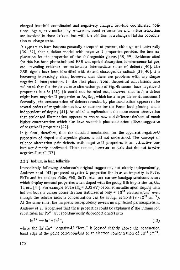
charged four-fold coordinated and negatively charged two-fold coordinated posi- tions. Again, as visualized by Anderson, bond reformation and lattice relaxation are involved in these defects, but with the addition of a change of lattice coordina- tion vs. charge state.
It appears to have become generally accepted at present, although not universally [36, 37], that a defect model with negative-U properties provides the best ex- planation for the properties of the chalcogenide glasses [38, 39]. Evidence cited for this has been photo-induced ESR and optical absorption, luminescence fatigue, etc., revealing evidence for metastable intermediate states of defects [40]. The ESR signals have been identified with As and chalcogenide radicals [39, 40]. It is becoming increasingly clear, however, that there are problems with any simple negative-U interpretation. In the first place, recent theoretical calculations have indicated that the simple valence alternation pair of Fig. 4b cannot have negative-U properties in a-Se [35]. (It could not be ruled out, however, that such a defect might have negative-U properties in As2 Se3, which has a larger dielectric constant.) Secondly, the concentration of defects revealed by photoexcitation appears to be several orders of magnitude too low to account for the Fermi level pinning, and is independent of doping [41]. An added complication is the more recent observation that prolonged illumination appears to create new and different defects of much higher concentration which also have reversible photoexcitation effects suggestive of negative-U properties [ 42 ].
It is clear, therefore, that the detailed mechanism for the apparent negative-U properties of doped chalcogenide glasses is still not understood. The concept of valence alternation pair defects with negative-U properties is an attractive one but not directly confirmed. There remain, however, models that do not involve negative-U at all [37 ].
2.2.2 Indium in lead telluride
Immediately following Anderson's original suggestion, but clearly independently, Andreev et al. [43] proposed negative-U properties for In as an impurity in PbTe. PbTe and its analogs PbSe, PbS, SnTe, etc., are narrow bandgap semiconductors which display unusual properties when doped with the group IIIb impurities In, Ga, T1, etc. [44]. For example, PbTe (Eg = 0.32 eV) becomes metallic upon doping with indium but the carrier concentration stabilizes at only ~ I0 is electrons/cm 3 even though the soluble indium concentration can be as high as 20 % (3 �9 10 zl cm-3). At the same time, the magnetic susceptibility reveals no significant paramagnetism.
Andreev et al. recognized that these properties could be explained if the indium ion substitutes for Pb 2 + but spontaneously disproportionates into
In 2+ ---+ In + + In a+, (12)
where the In+/In 3+ negative-U "level" is located slightly above the conduction band edge at the point corresponding to an electron concentration of 10 's cm -3.
170
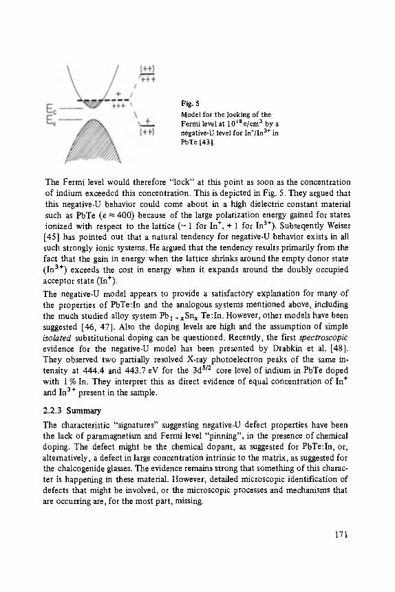
Fig. 5 Model for the locking of the Fermi level at 101Se/cm a by a negative-U level for In§ 3+ in PbTe [431.
The Fermi level would therefore "lock" at this point as soon as the concentration of indium exceeded this concentration. This is depicted in Fig. 5. They argued that this negative-U behavior could come about in a high dielectric constant material such as PbTe (e ~ 400) because of the large polarization energy gained for states ionized with respect to the lattice ( - 1 for In +, + 1 for In3+). Subseqently Weiser [45] has pointed out that a natural tendency for negative-U behavior exists in all such strongly ionic systems. He argued that the tendency results primarily from the fact that the gain in energy when the lattice shrinks around the empty donor state (In 3+) exceeds the cost in energy when it expands around the doubly occupied acceptor state (In+).
The negative-U model appears to provide a satisfactory explanation for many of the properties of PbTe:In and the analogous systems mentioned above, including the much studied alloy system Pb I _xSn x Te:In. However, other models have been suggested [46, 47]. Also the doping levels are high and the assumption of simple isolated substitutional doping can be questioned. Recently, the first spectroscopic evidence for the negative-U model has been presented by Drabkin et al. [48]. They observed two partially resolved X-ray photoelectron peaks of the same in- tensity at 444.4 and 443.7 eV for the 3d s/2 core level of indium in PbTe doped with 1% In. They interpret this as direct evidence of equal concentration of In + and In 3+ present in the sample.
2.2.3 Summary
The characteristic "signatures" suggesting negative-U defect properties have been the lack of paramagnetism and Fermi level "pinning", in the presence of chemical doping. The defect might be the chemical dopant, as suggested for PbTe:In, or, alternatively, a defect in large concentration intrinsic to the matrix, as suggested for the chalcogenide glasses. The evidence remains strong that something of this charac- ter is happening in these material. However, detailed microscopic identification of defects that might be involved, or the microscopic processes and mechanisms that are occurring are, for the most part, missing.
171
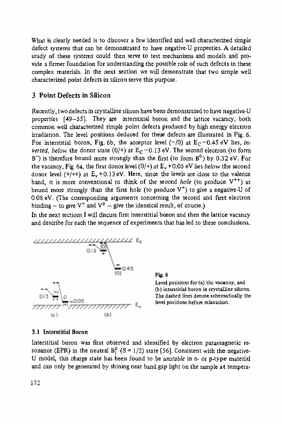
What is clearly needed is to discover a few identified and well characterized simple defect systems that can be demonstrated to have negative-U properties. A detailed study of these systems could then serve to test mechanisms and models and pro- vide a firmer foundation for understanding the possible role of such defects in these complex materials. In the next section we will demonstrate that two simple well characterized point defects in silicon serve this purpose.
3 Point Defec t s in Sil icon
Recently, two defects in crystalline silicon have been demonstrated to have negative-U properties [49-55]. They are interstitial boron and the lattice vacancy, both common well characterized simple point defects produced by high energy electron irradiation. The level positions deduced for these defects axe illustrated in Fig. 6. For interstitial boron, Fig. 6b, the acceptor level ( - /0) at E c -0 .45 eV lies, in- verted, below the donor state (0/+) at E c -0 .13 eV. The second electron (to form B-) is therefore bound more strongly than the first (to form B ~ by 0.32 eV. For the vacancy, Fig. 6a, the first donor level (0/+) at Ev + 0.05 eV lies below the second donor level (+/++) at Ev+0.13eV. Here, since the levels are close to the valence band, it is more conventional to think of the second hole (to produce V ++) as bound more strongly than the first hole (to produce V +) to give a negative-U of 0.08 eV. (The corresponding arguments concerning the second and first electron binding - to give V § and V ~ - give the identical result, of course.)
In the next sections I will discuss first interstitial boron and then the lattice vacancy and describe for each the sequence of experiments that has led to these conclusions.
Fig, 6 Level positions for (a) the vacancy, and (b) interstitial boron in crystalline silicon. The dashed lines denote schematically the level positions before relaxation.
3.1 Interstitial Boron
Interstitial boron was first observed and identified by electron paramagnetic re- sonance (EPR) in the neutral B ~ (S = 1/2) state [56]. Consistent with the negative- U model, this charge state has been found to be unstable in n- or p-type material and can only be generated by shining near band gap light on the sample at tempera-
172
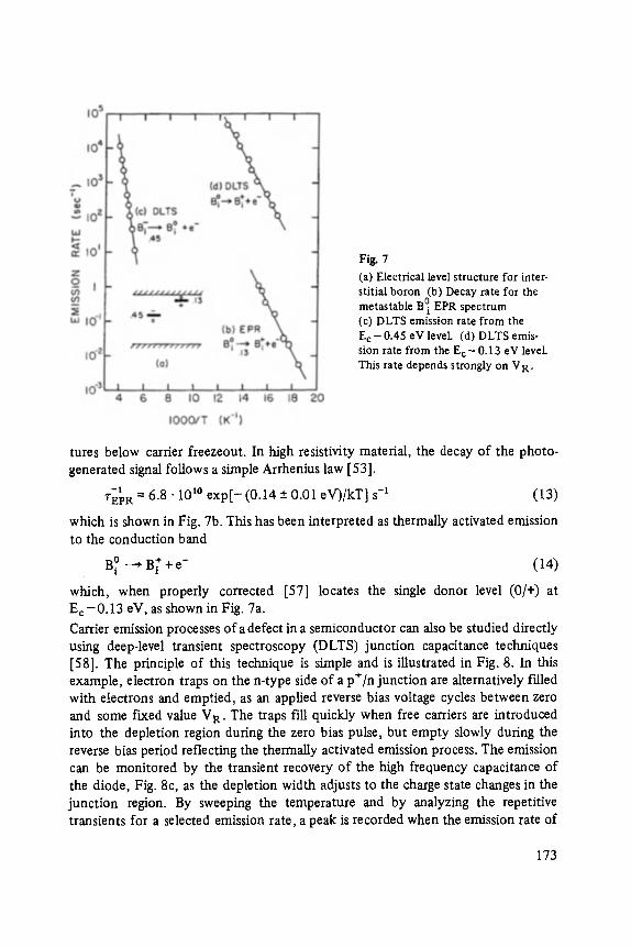
Fig. 7 (a) Electrical level structure for inter- stitial boron (b) Decay rate for the metastable B] EPR spectrum (c) DLTS emission rate from the E c - 0.45 eV level (d) DLTS emis- sion rate from the E c -0.13 eV level. This rate depends strongly on V R.
tures below carrier freezeout. In high resistivity material, the decay of the photo- generated signal follows a simple Arrhenius law [53].
"/'EPR-I = 6.8 �9 101~ exp[ - (0,14 -+ 0.01 eV)/kT] s -1 (13)
which is shown in Fig. 7b. This has been interpreted as thermally activated emission to the conduction band
o ~ B + + e- (14) Bi
which, when properly corrected [57] locates the single donor level (0]+) at E c -0 .13 eV, as shown in Fig. 7a.
Carrier emission processes e ra defect in a semiconductor can also be studied directly using deep-level transient spectroscopy (DLTS) junction capacitance techniques [58]. The principle of this technique is simple and is illustrated in Fig. 8. In this example, electron traps on the n-type side of a p+]n junction are alternatively Idled with electrons and emptied, as an applied reverse bias voltage cycles between zero and some fixed value V R. The traps fill quickly when free carriers are introduced into the depletion region during the zero bias pulse, but empty slowly during the reverse bias period reflecting the thermally activated emission process. The emission can be monitored by the transient recovery of the high frequency capacitance of the diode, Fig. 8c, as the depletion width adjusts to the charge state changes in the junction region. By sweeping the temperature and by analyzing the repetitive transients for a selected emission rate, a peak is recorded when the emission rate of
173
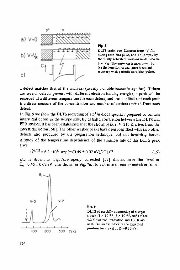
Fig. 8 DLTS technique. Electron traps (a) flU during zero bias pulse, and (b) empty by thermally activated emission under reverse bias V R. The emission is monitored by (c) the junction capacitance transient recovery with periodic zero bias pulses.
a defect matches that of the analyzer (usually a double boxcar integrator). If there are several defects present with different electron binding energies, a peak will be recorded at a different temperature for each defect, and the amplitude of each peak is a direct measure o f the concentration and number of carriers emitted f rom each defect.
In Fig. 9 we show the DLTS recording of a p*/n diode specially prepared to contain interstitial boron in the n-type side. By detailed correlation between the DLTS and EPR studies, it has been established that the strong peak at ~ 210 K arises from the interstitial boron [50]. The other weaker peaks have been identified with two other defects also produced by the preparation technique, but not involving boron.
A study of the temperature dependence of the emission rate of this DLTS peak gives
ee ~ 6.2 �9 1013 e x p [ - (0.49 --- 0.02 eV)/kT] s -1 (15)
and is shown in Fig. 7c. Properly corrected [57] this indicates the level at E c - 0 . 4 5 + 0.02 eV, also shown in Fig. 7a. No evidence of carrier emission from a
Fig. 9 DLTS of partially counterdoped n-type silicon (1 x 10¹⁶B, 3 x 10¹⁶P/cm 3) after 4.2 K electron irradiation and 100 K an- neal The arrow indicates the expected position for a level at Ec-0.13 eV.
174
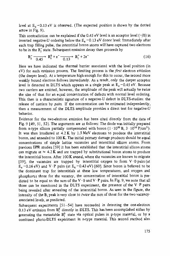
level at E e -0 .13 eV is observed. (The expected position is shown by the dotted arrow in Fig. 9).
This contradiction can be explained if the 0.45 eV level is an acceptor level ( - /0) in inverted negative-U ordering below the E e -0 .13 eV donor level: Immediately after each trap filling pulse, the interstitial boron atoms will have captured two electrons to be in the B~" state. Subsequent emission decay then proceeds by
+
B~" 0.45 ' B~ +e- 0.13 r Bi +2e- (16)
Here we have indicated the thermal barrier associated with the level position (in eV) for each emission process. The limiting process is the first electron emission (the deeper level). At a temperature high enough for this to occur, the second more weakly bound electron follows immediately. As a result, only the deeper acceptor level is detected in DLTS which appears as a single peak at E e -0 .45 eV. Because two carriers are emitted, however, the amplitude of the peak will actually be twice the size of that for an equal concentration of defects with normal level ordering. This then is a characteristic signature of a negative-U defect in DL'l'S-studies: the release of carriers by pairs. If the concentration can be estimated independently, then a measurement of the DLTS amplitude provides a direct test for negative-U behavior.
Evidence for the two-electron emission has been cited directly from the data of Fig. 9 [49, 51, 52]. The arguments are as follows: The diode was initially prepared from n-type silicon partially compensated with boron (1 �9 1016 B, 3 ' 1016P/cm3). It was then irradiated at 4.2 K by 1.5 MeV electrons to produce the interstitial boron, and annealed to 100 K. The initial primary damage products should be equal concentrations of simple lattice vacancies and interstitial silicon atoms. From previous EPR studies [59] it has been established that the interstitial silicon atoms can migrate at ~ 4.2 K and are trapped by substitutional boron atoms to produce the interstitial boron. After 100 K anneal, where the vacancies are known to migrate [59], the vacancies are trapped by interstitial oxygen to form V . 0 p a i r s ( a t Ee-0 .16 eV) and V .P pairs (at Ec -0 .43 eV) [60]. Since boron is believed to be the dominant trap for interstitials at these low temperatures, and oxygen and phosphorus those for the vacancy, the concentration of interstitial boron is pre- dicted to be equal to the sum of the V. 0 and V- P pairs. In Fig. 9, we note that all three can be monitored in the DLTS experiment, the presence of the V-P pairs being revealed after annealing of the interstitial boron. As seen in the figure, the intensity of the B i peak is very close to twice the sum of those for the two vacancy-
associated levels, as predicted. Subsequent experiments [51-54] have succeeded in detecting the one-electron 0.13 eV emission from B ~ directly in DLTS. This has been accomplished either by generating the metastable B ~ state via optical pulses in p-type material, or by a combined photo-DLTS experiment in n-type material. This second method also
175
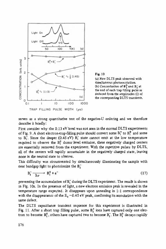
Fig. 10 (a) New DLTS peak observed with simultaneous photoexcitation. (b) Concentration of B 0 and B~ at the end of each trap filling pulse as deduced from the amplitudes (I) of the corresponding DLTS transients.
serves as a strong quantitative test of the negative-U ordering and we therefore describe it briefly:
First consider why the 0.13 eV level was not seen in the normal DLTS experiments of Fig. 9. A short electron-trap-filling pulse should convert some B + to B ~ and some to B~. Since the deeper (0.45 eV) B~" state cannot emit at the low temperature required to observe the B ~ donor level emission, these negatively charged centers are essentially removed from the experiment. With the repetitive pulses by DLTS, all of the centers will rapidly accumulate in the negatively charged state, leaving none in the neutral state to observe.
This difficulty was circumvented by simultaneously illuminating the sample with near bandgap light to photoionize the B~
B~ hv ' B~ (17)
preventing the accumulation of B~- during the DLTS experiment. The result is shown in Fig. 10a. In the presence of light, a new electron emission peak is revealed in the temperature range expected. It disappears upon annealing in 1:1 correspondence with the disappearance of the E c -0.45 eV peak, confirming its association with the same defect.
The DLTS capacitance transient sequence for this experiment is illustrated in Fig. 1 I. After a short trap fiUing pulse, some B + ions have captured only one elec- tron to become B ~ others have captured two to become B~. The B ~ decays rapidly
176
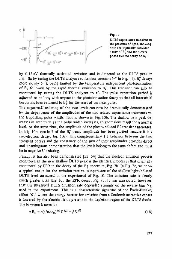
Fig. 11 DLTS capacitance txansient in the presence of light, showing both the thermally activated decay of B~ and the slower photo-excited decay of B~ .
by 0.13 eV thermally activated emission and is detected as the DLTS peak in Fig. 10a by tuning the DLTS analyzer to its time constant (r ~ in Fig. 1 I). B[ decays more slowly (r-), being limited by the temperature independent photoionization of B[ followed by the rapid thermal emission to B~'. This transient can also be monitored by tuning the DLTS analyzer to r-. The pulse repetition period is adjusted to be long with respect to the photoionization decay so that all interstitial boron has been returned to B~" for the start of the next pulse.
The negative-U ordering of the two levels can now be dramatically demonstrated by the dependence of the amplitudes of the two related capacitance transients vs. the trap-filling pulse width. This is shown in Fig. 10b. The shallow new peak de. creases in amplitude as the pulse width increases, an anomalous result for a normal level. At the same time, the amplitude of the photo-induced B[ transient increases. In Fig. 10b, one-half of the B[ decay amplitude has been plotted because it is a two-electron decay, Eq. (16). This complementary 1:1 behavior between the two transient decays and the constancy of the sum of their amplitudes provides direct and unambiguous demonstration that the levels belong to the same defect and must be in negative-U ordering.
Finally, it has also been demonstrated [53, 54] that the electron emission process monitored in the new shallow DLTS peak is the identical process as that originally monitored by EPR in the decay of the B ~ spectrum, Fig. 7b. In Fig. 7c, we show a typical result for the emission rate vs. temperature of the shallow light-induced DLTS level measured in the experiment of Fig. 10. The emission rate is clearly much greater than that for the EPR decay, Fig. 7b. It was also noted, however, that the measured DLTS emission rate depended strongly on the reverse bias V R used in the experiment. This is a characteristic signature of the Poole-Frenkel effect [61] where the energy barrier for emission from a Coulomb attractive center is lowered by the electric fields present in the depletion region of the DLTS diode. The lowering is given by
AE B = e(ehreeo)~/2 a 1/2 = ~ i]2 (18)
177
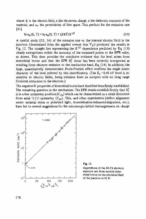
where g is the electric field, e the electronic charge, e the dielectric constant of the material, and eo the permittivity of free space. This predicts for the emission rate [61]
In en(~, T) = In en(O, T) + (3/kT)g 1/2 (19)
A careful study [53, 54] of the emission rate vs. the internal electric field in the junction (determined from the appLied reverse bias V R) produced the results in Fig. 12. The straight line representing the &1/2 dependence predicted by Eq. (19) clearly extrapolates within the accuracy of the measured points to the EPR value, as shown. This then provides the conclusive evidence that the level arises from interstitial boron and that the EPR I3_ ~ decay has been correctly interpreted as resulting from electron emission to the conduction band, Eq. (14). In addition, the large, quantitatively demonstrated Poole-Frenkel effect confirms the single donor character of the level inferred by this identification. (The E c -0.45 eV level is in. sensitive to electric fields, being emission from an acceptor with no long range Coulomb attraction to the electron.)
The negative-U properties of interstitial boron have therefore been fLrmly established. The remaining question is the mechanism. The EPR results establish firmly that B ~ is in a low symmetry position (C lh) which can be characterized as a small distortion from axial (111)symmetry (C3v). This, and other experiments (defect alignment under uniaxial stress or polarized light, recombination-enhanced-migration, etc.), have led to several suggestions for the microscopic lattice rearrangements vs. charge
Fig. 12
Dependence of the DLTS electron emission rate from neutral inter- stitial boron on the electrical field of the junction at 65 K.
178

Fig. 13 Suggested model for the lattice configurations of inter- stitial borons vs. charge state 150, 561.
Fig. 14 Alternate model for the interstitial boron configurations [50, 561. Shown are the lattice atoms and the normal interstitial tetra- hedral (T) and hexagonal (H) sites in a {110} plane.
state [50, 56]. One is shown in Fig. 13, where the ion flips from a bond-centered configuration for B~ to a split-(100) bonded configuration for B 7. Another is shown in Fig. 14, where the defect moves between the hexagonal interstitial site for B~ to the (100)-split configuration. The intermediate configuration for B ~ in either model is consistent with the EPR results. Other models have also been suggested [56]. At present, we cannot distinguish between these. However, the prospects are good that we may soon be able to establish the actual configurations involved. This optimism stems, on the experimental side, from the good fortune to have the pre- cise EPR probe for the intermediate B ~ state, and, on the theoretical side, f rom the emergence of quantum mechanical defect calculations that appear to give reliable total energies [35, 62 -64] so that the relaxed configurations of such a simple defect may be evaluated.
In any case, the observed dangling bond character of the EPR B ~ state and the changes in lattice coordination indicated in the various proposed models suggest that this system should be considered a close analogue of the valence alternation pair models of Kastner et al. [33].
3.2 Vacancy in Silicon
In this case we can reverse the presentation. The mechanism for negative-U behavior is known. EPR studies of the V + and V- paramagnetic charge states of the vacancy [59] have revealed large static tetragonal distortions, the four dangling bonds tend- ing to reconstruct by pairs as shown in Fig. 15. This has been viewed as a Jahn-
179

Fig. 15 Tetragonal Jahn-TeUer distortion of the vacancy and the negative-U ordering of the first and second donor states that results.
Teller distortion resulting from partial occupancy of triply degenerate t2 gap orbitals made up from these dangling bonds. For V § before distortion, the con- figuration is t~, for V ~ t~, etc. The formalism introduced by Anderson [17], Eqs. (9) and (10), is therefore directly applicable where X becomes the single- electron Jahn-TeUer coupling coefficient, x, a coordinate for the bond-pairing tetragonal distortion, and c, the elastic restoring force constant on the four atoms surrounding the vacancy. I f ),2/c > U, Uef f becomes negative. In this case, the Jahn- Teller energy gained by electron pairing to form V ~ exceeds the Coulomb repulsion energy U, and the (0/+) and (+/++) levels cross as indicated in the figure.
The remarkable fact is that negative-U behavior between these three charge states was predicted [65-67] before it was experimentally confirmed. On the basis of theoretical calculations, Baraff et al. estimated X, c, and U and concluded that the vacancy should be a negative-U system. We will now outline the subsequent experimental confirmation.
The experiments closely parallel those for interstitial boron:
(1) The V + state seen by EPR is metastable. No Fermi level position has been found for it to be the stable charge state. It must be photogenerated. (2) The V § EPR signal decay after photogeneration is given by [59]
r -1 = 8" 101~ exp[( - 0.057 -+ 0.004 eV)/kT] s -~ (20)
and is shown in Fig. 16b. Interpreting this as hole release to the valence band,
V + ~ V ~ + h + (21)
locates the single donor level (0/+) at ~ Ev + 0.05 eV [57], as shown in Fig. 16a. (3) DLTS studies [68] reveal a hole emission peak associated with the vacancy with emission rate
eh DLTS = 5 " 1011 e x p [ ( - 0 . 1 4 -+ 0.01 eV)/kT] s -1 (22)
180

Fig. 16 (a) Electrical level structure for the two donor states of the vacancy. (b) Decay rate for the metastable V § EPR spectrum. (c) DLTS emission rate for the Ev+ 0.13 eV level
as shown in Fig. 16c. The DLTS peak displays no Poole-Frenkel effect, which identifies it as a donor, with no long range Coulomb attraction to the emitted hole [55]. The corresponding electrical level position [57] is at Ev + 0.13 eV, as shown in Fig. 16a. (4) Negative-U ordering implies that the Ev+0.13 eV peak is a two hole release
V § ~ V + + h + ~ V ~ +, (23) 0.13 O.05
the first deeper hole (0.13 eV binding) providing the rate limiting process, the second hole (0.05 eV binding) following immediately. The initial evidence cited for this [49] is summarized in Fig. 17. Fig. 17a shows the DLTS spectrum in p-type floating zone silicon containing 1018 Sn/cm a which had been irradiated at 4.2 K by 1.5 MeV electrons. The spectrum is shown before and after annealing at 200 K. From pre- vious EPR studies [59, 69] and the kinetics of the annealing observed in the DLTS
181
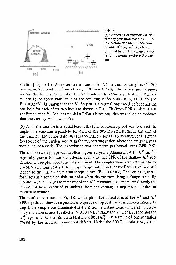
Fig. 17 (a) Conversion of vacancies to tin- vacancy pairs monitored by DLTS in electron-irradiated silicon con- taining 10 is Sn/cm 3. (b) When captured by tin, the vacancy levels return to normal positive-U order- ing.
studies [49], ~ 100 % conversion of vacancies (V) to vacancy-tin pairs (V.Sn) was expected, resulting from vacancy diffusion through the lattice and trapping by tin, the dominant impurity. The amplitude o f the vacancy peak at Ev + 0.13 eV is seen to be about twice that of the resulting V- Sn peaks at Ev + 0.07 eV and Ev + 0.32 eV. Assuming that the V �9 Sn pair is a normal positive-U defect emitting one hole for each of its two levels as shown in Fig. 17b (from EPR studies it was confirmed that V �9 Sn ~ has no Jahn-Teller distortion), this was taken as evidence that the vacancy emits two holes.
(5) As in the case for interstitial boron, the final conclusive proof was to detect the single hole emission separately for each of the two inverted levels. In the case of the vacancy, the donor state (0/+) is too shallow for DLTS measurements (strong freeze-out of the carriers occurs in the temperature region where the emission peak would be observed). The experiment was therefore performed using EPR [55].
The samples were p-type vacuum-floating-zone crystals (Aluminum, 4.1 �9 1 olS cm-3), especially grown to have low internal strains so that EPR of the shallow Als o sub- stitutional acceptor could also be monitored. The samples were irradiated in situ by 2.4 MeV electrons at 4.2 K to partial compensation so that the Fermi level was still locked to the shallow aluminum acceptor level (Ev + 0.07 eV). The acceptor, there- fore, acts as a source or sink for holes when the vacancy changes charge state. By monitoring the changes in intensity o f the Als o resonance, one measures directly the number o f holes captured or emitted from the vacancy in response to optical or thermal excitation.
The results are shown in Fig. 18, which plots the amplitudes o f the V + and Also EPR signals vs. time for a particular sequence of optical and thermal excitations. In step I, the sample was illuminated at 4.2 K from a distant room temperature black- body radiation source (peaked at ~ 0.13 eV-). Initially the V + signal is zero and the Al~ signals is 0.24 of its preirradiation value, (Al~ , as a result of compensation (76%) by the irradiation-produced defects. Under the 300 K illumination, a 1 : 1
182
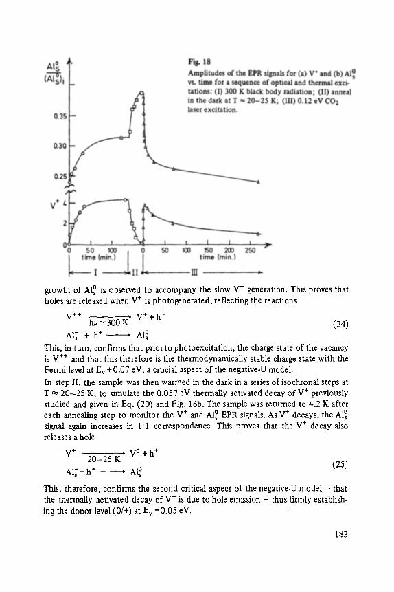
growth of Als o is observed to accompany the slow V § generation. This proves that holes are released when V + is photogenerated, reflecting the reactions
V ++ ~ V + + h + h~ ~300 K (24)
A1 s + h+--------~ Als o
This, in turn, confirms that prior to photoexcitation, the charge state of the vacancy is V ++ and that this therefore is the thermodynamically stable charge state with the Fermi level at Ev + 0.07 eV, a crucial aspect of the negative-U model.
In step II, the sample was then warmed in the dark in a series of isochronal steps at T ~ 2 0 - 2 5 K, to simulate the 0.057 eV thermally activated decay of V + previously studied and given in Eq. (20) and Fig. 16b. The sample was returned to 4.2 K after each annealing step to monitor the V § and Also EPR signals. As V § decays, the Als o signal again increases in 1:1 correspondence. This proves that the V + decay also releases a hole
V + ~ V ~ + h + 20"25 K
At; +h + ~ Also (25)
This, therefore, confirms the second critical aspect of the negative-U model - that the thermally activated decay of V + is due to hole emission - thus firmly establish- ing the donor level (0/+) at E v + 0.05 eV.
183
In step III, the sample was then illuminated with ~ 1 mW of CO2 laser irradiation (0.12 eV). The neutral vacancies rapidly capture holes (from the photoionized acceptors)
Als~ hv = 0.12 eX ~ Als + h+ V ~ + h + > V + (27)
and the vacancy-acceptor system returns quickly to the conditions that existed prior to the 20-25 K anneal. With continued CO2 illumination, the positively charged vacancies eventually capture a second hole
V + + h + ~ V ++
finally returning the system to the charge states at the beginning of the experiment, thus completing the cycle.
All aspects of the negative-U ordering have therefore been confirmed. The shallow level at Ev + 0.05 eV has been shown to be the single donor level. The level at Ev+ 0.13eV, also demonstrated to be a donor, must therefore be the second donor. The deduction from the DLTS studies of two-hole emission from the Ev+0.13eV level has been directly and unambiguously demonstrated in the photo-EPR studies of Fig. 18, by separating the two emission processes. The first deeper hole is emitted when the V + charge state is photogenerated with lap ~> 0.13 eV (the CO2 laser does not activate this), and the second shallower hole is subsequently emitted by thermal activation from V +.
For completeness, one point of current controversy should be mentioned. As described earlier in the text, Hall measurements should detect the virtual level E(0/++), halfway between the two inverted levels. Recognizing this, Mukashev at al. [70] have recently reanalyzed earlier Hall measurements [71] and extracted a vacancy level
E(0/++) = (0.084 _+ 0.004) eV,
in very good agreement with the level structure of Fig. 16. This has subsequently been challenged by Hoffmann [72], however, who, by applying his recently suggested test for negative-U behavior [2], concluded that the data could be better fit by a single normal level at that position. We now know that the vacancy is a negative-U defect and we know with precision the positions of the two inverted levels. It would be highly desirable, therefore, to perform careful new Hall measurements (in the dark) designed specifically to test Hoffmann's theory on this system.
4 Discussion
Interstitial boron and the lattice vacancy in crystalline silicon have been demonstrat- ed conclusively to have negative-U properties. As such, we believe that they represent the first and only defects in any solid to have been unambiguously identified to
184

have this property. In the case of the lattice vacancy, the driving force for the behavior has been identified as a Jahn-Teller distortion. The symmetry of the distortion is tetragonal, which is a bondqike formation by pairs between the partially occupied four dangling bonds of the neighbors. This, therefore, is an example of the model conceived by Anderson [ 17], but at a defect as visualized by Street and Mott [32]. The detailed mechanism for interstitial boron has not as yet been established but appears to involve rebonding and lattice coordination change for the ion, also visualized by Street and Mott and in close analogy to the valence alternation pair models of Kastner et al. [33].
This first observation of well identified simple point defects with negative-U be- havior could be very important. I have already discussed the evidence for such defects in the chalcogenide glasses and in the PbTe:In and related systems. What we are learning in microscopic detail for these simple point defects in silicon can serve as a model for understanding the possible role of negative-U defects in these more complex systems. We are also learning new and precise ways to study and characterise them: photo-DLTS, two carrier release, different Hall and DLTS properties, photo-EPR, etc. We have confirmed that large lattice relaxations are involved, the energy gained in electron pair bond formation or rearrangement serving to override the Coulomb repulsion between the electrons. This implies large electron-lattice couplings which can be expected to manifest themselves in other properties for the defects as well: large Stokes shifts for optical properties, multiphonon capture for charged carriers, radiationless recombination, recombination-enhanced migration, etc. It is interest- ing to note that both interstitial boron and the lattice vacancy have recently been demonstrated to migrate athermally at cryogenic temperatures under photo- or electronic excitation [50, 68, 73]. These features provide, therefore, additional signatures for possible negative-U behavior.
Much of the current literature concerning negative-U properties has dealt with amorphous materials. Indeed, many of the models are specific to such systems. The direct confirmation described here of negative-U properties for simple defects in crystalline silicon reveals that the phenomenon is more fundamental and universal. How prevalent are negative-U defects then? Have such defects been present all along and simply not detected because we didn't know what to look for, or weren't suspicious? In the crystalline semiconductors, for instance, electrical level positions for many defects and impurities have been measured and tabulated. Are some of these also negative-U centers? We have learned now that making one type of meas- urement, the usual procedure, is not sufficient. The key in electrical measurements is that DLTS and Hall measurements give different results, photo-DLTS produces "new" levels, etc. Another interesting fact is that if the inverted levels of a negative- U defect straddle the middle of the forbidden gap, the defect will not be detected at all in conventional DLTS or Hall studies. How many important defects have been missed entirely?
185
What new exotic electronic properties might be available for a solid with such defects? Metastability implies reversible memory and switching effects, for one thing. How about possible superconducting effects? As mentioned in the intro- duction, a defect with negative-U properties can be considered an "extrinsic Cooper pair", the defect supplying a localized region for enhanced electron pairing. This
has recently been considered and suggested to explain enhanced superconducting behavior in A1-Ge, AI-Si, and Be-Si eutectic alloys [74, 75].
Another piece of evidence is in the reported superconducting properties of PbTe:T1, where the much studied In dopant has been replaced by the analogous but more
disproportionating T1 dopant [76].
Finally, what would y o u do, if you could incorporate a "tailored" negative-U defect
into your material or device?
Acknowledgement The experimental work reviewed in this paper concerning defects in silicon was performed over the past few years at Lehigh University by my graduate students, J. R. TroxeU, R. D. Harris, A. P. Chatterjee, and J. L. Newton, and with support from the Office of Naval Research under contract N00014-76-1097. I thank the Max-Planck-lnstitut for Solid State Research, Stuttgart, and the IV Physical Institute, University of Stuttgart for their hospitality. I thank also the Alexander-yon-Humboldt-Foundation for the Senior U. S. Scientist Award which made my stay in the Federal Republic of Germany possible.
References
[ll 3". Hubbard, Proc. Roy. Soc. A276, 238 (1963). [21 H.J. Hoffmann, Appl. Phys. A27, 39 (1982). In this paper Hoffmann notes subtle differ-
ences between the Hall properties for normal and negative-U levels that he argues should be detectable under careful analysis.
[31 L.N. Cooper, Phys. Rev. I04, 1189 (1956). [41 See, for example, John Burgess, Metal Ions in Solution, Chiehester, Ellis Horwood Ltd.,
1978. [5] G. Milazzo andS. Caroli, Table of Standard Electrode Potentials, New York, Wfley, 1978.
[61 Handbook of Chemistry and Physics, 60th edn., Boca Raton, CRC Press, 1980, pgs. D-155-160.
[71 W. Weyl, Pogg. Ann. 121,601 (1863). [81 The recent evolution of this fascinating topic is chronicled in the published proceedings
of the international "CoUoque Weyl" conferences: I. Metal Ammonia Solutions, ed. by G. Lepourtre and M. J. Sienko, N. Y., Benjamin, 1964; II. Metal Ammonia Solutions, ed. by 9". J. Lagowski andM. J. Sienko, London, Butterworths 1970; III. Electrons in Fluids, ed. by J. Jortner andN. R. Kastner, Berlin, Springer-Verlag 1973; IV. J. Phys. Chem. 79, 2789-3079 (1975); V. J. Phys. Chem. 84, 1065-1298 (1980). See also 34. H. Cohen and J. C. Thompson, Adv. Phys. 18, 665 (1969).
[91 R.A . Ogg. Jr., J. Am. Chem. Soe. 68, 155 (1946). [101 R.A. Ogg. Jr., J. Chem. Phys. 14, 114 (1946).
186
[11
[12
[13
[14
115
[16
117
[18
[19
[201
[211
1221 [23]
[241
[251
[26]
I27]
[281
[291
1301
1311
1321 [33]
1341
135]
[36]
I371
1381
1391 [401
1411
[421
[431
R. A. Ogg. Jr., J. Chem. Phys. 14,295 (1946).
S. Freed and N. Sugarman, J. Chem. Phys. 11,354 (1943).
J. Kaplan and C Kittel, J. Chem. Phys. 21, 1429 (1953).
R. H. Land andD. E. O'Reilly, J. Chem. Phys. 46,4496 (1967).
M. D. Newton, J. Phys. Chem. 79, 2795 (1975).
J. L. Dye, C. Ir Andrews, andJ. M. Ceraso, J. Phys. Chem. 79, 3076 (1975).
P. W. Anderson, Phys. Rev. Lett. 34,953 (1975).
V. L. Vinetskii, Zh. Eksp. Teor. Fiz. 40, 1459 (1961) [Sov. Phys. JETP 13, 1023 (1961)1.
T. D. Shultz, in Polaxons and Exeitons, ed. by C. G. Kuper and G. D. Whitfield, New York, Plenum 1962, p. 110. S. Laskis, C. Schlenker, B. K. Chakraverty, R. Buder, and M. Marezio, Phys. Rev. B 14, 1429 (1976). C. Schlenker, S. Ahmed, R, Buder, and M. Gourmala, J. Phys. C 12, 3503 (1979).
O. F. Schirmer andE. Sal/e, J. Phys. C 13, L1067 (1980).
T. M. Rice and L. Sneddon, Phys. Rev. Lett. 47,689 (1981).
M. Peo, S. Roth, K. Dransfeld, B. Tieke, J. Hocker, H. Gross, A. Grupp, and H. Sixl, Sol. St. Comm. 35,119 (1980). J. L. Bredas, R. R. Chance, and R. Silbey, Phys. Rev. B 26, 5843 (1982).
C. Crecelius, M. Stamm, J. Fink, andJ. J. Ritsko, Phys. Lett. 50, 1498 (1983).
iV. A. Cade andB. Movaghar, J. Phys. C 16,539 (1983).
J. C. Scott, P. Pfluger, M. T. Krounbi, and G. B. Street, Phys. Rev. B 28, 2140 (1983),
A. Alexandrov andJ. Ranninger, Phys. Rev. B 24, 1164 (1981).
B. K. Chakraverty, J. Physique 42, 1351 (1981). S. A. Brazovskii and N. N. Kirova, Pis. Zh. Eksp. Teor. Fiz. 33, 6 (1981) [JETP Lett. 33, 4 (I98i)1. R. A. Street and N. F. Mott, Phys. R~v. Lett. 35, 1293 (1975). M. Kastner, D. Adler, and H. Fritzsche, Phys.Rev.Lett. 37, 1504 (1976).
Kastner et al. originally suggested that the neutral state would also be threefold co- ordinated. Subsequently, more detailed calculations by Vanderbilt and Joannopoulos [35] concluded that it would be singly coordinated.
D. Vanderbilt andJ. D. Joannopoulos, Phys. Rev. B 27, 6311 (1983).
D. C. Licciardello, D. L. Stein, and F. D. M. Haldane, PhiL Mag. B 43, 189 (1981).
D. Ernin, Comments Sol. St. Phys. 11, 35 and 59 (1983).
See recent reviews by J'. Robertson, Phys. and Chem. of Glasses 23, 1 (1982) and Adv. in Phys. 32, 361 (1983).
H. Fritzsche, J. Phys. Soe. Japan 49, suppl. A, 39 (1980). S. G. Bishop, U. Strom, andP. C. Taylor, Phys. Rev. B 15, 2278 (1977).
G. Pfister, K. S. Liang, M. Morgan, P. C. Taylor, E. J. Friebele, and S. G. Bishop, Phys. Rev. Lett. 41, 1318 (1978). D. K. Biegelsen and R. A. Street, Phys. Rev. Lett. 44, 803 (1980).
Y. V. Andreev, K. I. Geiman, L A. Drabkin, A. V. Matveenko, E. A. Mozhaev, and B. Y. Moizhes, Fiz. Tekh. Poluprovodn. 9, 1873 (1975); [Soy. Phys. Semic. 9, 1235 (1975)].
187
[441 L A. Drabkin and B. Y. Moizhes, Fiz. Tekh. Poluprovodn. 15,625 (1981); [Soy. Phys. Semie. 15, 357 (1981)]. This also provides a good review of evidence for negative-U behavior of impurities in other systems. An interesting suggestion is made, for instance, that the MxWO 3 tungsten bronzes are examples of negative-U behavior of the alkali (M) ion dopant.
[45] K. Weiser, Phys. Rev. B 25, 1408 (1982).
[46] A.A . Averkin, V. I. Kaidanov, and R. B. Mel'nik, Fiz. Tekh. Poluprovodn. 5, 91 (1971); [Sov. Phys. Semic. 5, 75 (1971)].
[471 Y. Kagan and K. A. Kikoin, Pis. Eksp. Teor. Fiz. 31, 367 (1980) [JETP Lett. 31, 335 (1980)1.
1481 I .A. Drabkin, M. A. Kvantov, II. V. Kompaniets, and Y. P. Kostikov, Fiz. Tekh. Po- luprovodn. 16, 1276 (1982); [SOY. Phys. Semic. 16,815 (1982)1.
1491 G.D. Watkins and./. R. Troxell, Phys. Rev. Lett. 44,593 (1980).
[50I J.R. Troxell and G. D. Watkins, Phys. Rev. B 22,921 (1980).
1511 G.D. Watkins, A.P. Chatter]ee, and R. D. Harris, in Defects and Radiation Effects in Semiconductors, ed. by R. Hasiguti, London, Inst. of Phys. (Conf. Se. No. 59) 1981, p. 199.
1521 G.D. Watkins, in Defects in Semiconductors, ed. byJ. Narayan and T. Y. Tan, New York, North-Holland 1981, p. 21.
[531 R. D. Harrix, J. L. Newton, and G. D. Watkins, Phys. Rev. Lett. 48,1271(1982).
[541 R.D. Harris, Z L . Newton, andG. D. ICatkins, Phys. Rev. Lett. 51,1722(1983).
[551 J.L. Newton, A . P Chatter]ee, R .D. Harris, and G.D. Watkins, Physica I I6B, 219 (1983).
[561 G.D. I~atkins, Phys. Rev. B 12, 5824 (1975).
[57] After correction for the T 2 temperature dependence of the combined free carrier thermal velocity and density of states.
[581 G.L. Miller, D. 1I. Lang, andL. C. Kimerling, Ann. Rev. Mater. Sci. 7,377 (1977).
159] G.D. ICatkin~, in Lattice Defects in Semiconductors 1974, ed. by F. A. Huntley, London, Inst. of Phys. (Conf. Se. No. 23) 1975, p. 1.
1601 L. C Kimerling, in Radiation Effects in Semiconductors, ed. by F. A. Huntley, London, Inst. of Phys. (Conf. Se. No. 31) 1977, p. 221.
[611 3". Frenkel, Tech. Phys. USSR 5,685 (1938) and Phys. Rev. 54, 647 (1938). 1621 A. R. Williams, P. J. Feibelman, andN. D. Lang, Phys. Rev. B 26, 5433 (1982).
[631 G.A. Baraffand M. Schluter, Phys. Rev. B 28, 2296 (1983).
[641 R. Car, P. J. Kelly, A. Oshi/ama, andS. T. Pantelides, to be published.
1651 G. A. Baraff, E. O. Kane, and M. Schluter, Phys. Rev. Lett. 43,956 (1979).
[661 G.A. Baraff, E. O. Kane, and M. Schluter, Phys. Rev. B 21, 3563 (1980).
167] G.A. Baraff. E. O. Kane, andM. Schluter, Phys. Rev. B 22, 5662 (1980).
1681 G. D. ICatkins, J. R. Troxell, and A. P. Chatterjee, in Defects and Radiation Effects in Semiconductors 1978, ed. by Z H. Albany, London, Inst. of Phys. (Conf. Se. No. 46) 1979, p. 16.
1691 G.D. Watkins, Phys. Rev. B 12, 4383 (1975).
1701 B.N. Mukashev, V. V. Frolov, and L. G. Kolodin, Physics Letters 91A, 358 (1982).
188
[71] B. N. Mukashev, L. G. Kolodin, K. H. Nussupov, A. IF. Spitsyn, and V. S. Vavilov, Radiat. Eft. 46, 79 (1980).
1721 H.J. Hoffmann, Physics Letters 98 A, 444 (1983). 1731 G. D. Watkins, A. P. Chatter/ee, R. D. Harris, and J. R. Troxell, Semic. and Ins. 5, 321
(1983). 1741 E. Simanek, Sol. St. Comm. 32,731 (1979). 175] C.S. Ting, D. N. Talwar, and K. L. Ngai, Phys. Rev. Lett. 45, 1213 (1980). [761 L A. Chernik and S. iV. Likhov, Fiz. Tverd. Tela 23, 1400 (1981) [Soy. Phys. Sol. St. 23,
817 (1981)1.
189
Festk6rperprobleme XX IV (1984)
Chalcogens as Point Defects in Silicon
Peter Wagner, Claus Holm, Erhard Sirtl
Heliotronic GmbH, Burghausen, Federal Republic of Germany
Robert Oeder
Wacker-Chemie, Burghausen, Federal Republic of Germany
Werner Zulehner
Wacker-Chemitronic, Burghausen, Federal Republic of Germany
Summary: The elements of the chalcogen group form a large number of point-defects in silicon. "Pure" and "mixed" donor complexes are observed in S, Se, and Te doped Si in addition to isolated, probably substitutional, atoms. The tendency to form point-defect complexes increases from Te to O with increasing electronegativity and decreasing tetrahedral atomic radii. This tendency culminates for oxygen which may form a series of high-order complexes ("thermal donors") as well as precipitates depending on the specific thermal treatment. Ground and excited states of the different chalcogen centers are observed with infrared-absorption spectroscopy. With this method the formation kinetics of thermal donors may be investigated also. Examples for corresponding results are given and several models for thermal donors are discussed.
1 Introduction
Modern micro-electronics rely to a high extend on the exact knowledge of the behaviour of doping impurities and contaminants in Si. Included in this rather
general term are their electronic and thermodynamic properties.
The mostly used doping elements for silicon circuit device manufacturing are the group-III elements as acceptors or the group-V elements as donors. Electronic as well as thermodynamic properties of these impurities in Si are extensively studied and quite well understood. Metallic impurities usually are unwanted contaminants with the exception of gold and platinum which are used as life-time killers in certain devices. Most of the metallic impurities form electrically active centers in Si with much higher binding energies than the impurities used for doping. In addition to the two groups of impurities mentioned there is a third group having been studied extensively, to some extent even better understood than the doping dements : it is the group of the elements of the six th column of the periodic system, the chalco- gens O, S, Se, Te. The interest in these impurities in Si stems from several reasons:
191

- O is the most proliferant impurity in Si grown by the Czochralski-rnethod. It shows a special behaviour in terms of forming complexes and precipitates which is used in modern device technology (compare several papers in [1] e.g.)
- Se and Te are candidates for use in infrared detector devices [2] - S is a major contaminant in solar-grade Si produced by aluminotherrnic reduc-
tion from metallurgical Si [3]
In addition, fundamental physical aspects of impurities can be studied within the homologous series of the chalcogens, as will be demonstrated in the following sec- tions. Influence of site symmetry on energy level splitting, the transition from shallow to deep levels, the kinetics of complex formation and energy levels of complexes are objects of current investigations. The results of recent investigations will be reviewed in the present article with emphasis on infrared (IR) absorption experiments. This review and the corresponding quotations, by any means, cannot be complete, because work in this field is in full pace and many results are not completely under- stood, but the authors will try to create a feeling for the "complex" behaviour of the chalcogens in the true sense of the word and for the physical insights resulting from a study of these impurities.
After a short discussion of selected properties of chalcogens in the next section, in section 3 a description of the techniques of doping with chalcogens based on the authors' work is presented. The discussion of the point defects formed by S, Se, Te in section 5 is prepared by a short survey of the theory of donors in Si (section 4). Oxygen-related electrically active point defects and their complexing behaviour under thermal treatment (section 6) and a short summary (section 7) close the paper.
2 Selected Proper t ies o f C h a l c o g e n s
At the beginning of the discussion of the behaviour of chalcogens in Si a short comparison of the properties of the free atoms and some thermodynamic data not discussed further will be helpful. The electronic configuration of the outer shell of the free neutral chalcogen atoms is s2p 4 as compared to s2p 2 for Si. The chalcogens, therefore, have two electrons in excess, if they are incorporated in the Si-lattice on a Si-site. The binding energies for the s- and p-orbitals of the chalcogens are larger than those for Si. The differences to the corresponding values of Si as experimentally determined are shown in table 1. The differences of the tetrahedral radii between Si and the chalcogens are also shown. According to these data, O, S, Se should be incorporated easily on a substitutional site, Te might have difficulties. One also expects the substitutional chalcogens to be double donors: due to their higher ionization energies, they are able to bind electrons tighter than Si. In addi- tion, the solubilities and diffusion coefficients of the chalcogens in Si are also com- pared in table 1. With the exception of O no dependable solubility data are known, but O seems to have the highest solubility, followed by S. The diffusion coefficient
192
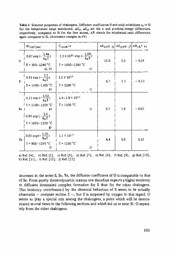
Table I Selected properties of ehal.cogens. Diffusion coefficients D and solid solubilities c s in Si for the temperature range mentioned. ,xE s, AEp are the s- and p-orbital energy differences, respectively, compared to Si for the free atoms, ,xR stands for tetrahedral radii differences, again compared to Si. (Activation energies in eV)
Se
Te
D/cm2/sec Cs/cm -3 AEs/eV j) 'XEp/eV j) ARIA~ h)
2.44. 0.07 exp (- k--~)
T = 300-1240 ~ a), b)
2.2 0.92 exp (- k--~-)
T = 1100-1300 "C d)
2.42 0.11 exp ( - k--~-)
T = 1100-1250 ~ e)
2.6 0.95 exp ( - k - ~ )
T = 1050-1250 ~ g)
3.34 0.05 exp (- --~o T )
T= 900-1250 ~ f)
1.08 2.2X 10²¹ exp ( - k ~ )
T = 1000-1280 ~ c)
2.5 X 10¹⁷
T = 1200 ~ i)
1.4-1.8 X 10¹⁷
T = 1200 ~ i)
1.1 X 10¹⁷
T : 1200 ~ i)
15.0 5.5
6.7 2.3
6.7
4.4
1.6
i 0.9
a) Ref. [4], b) Ref. [5], c) Ref. [6], d) Ref. [7], e) Ref. [8], f) Ref. [9], h) Ref . [ l l ] , i) Ref.[12], j) Ref.[13]
- 0 . 5 1
- 0 . 1 3
-0 .03
0.15
g) Ref. [10],
decreases in the series S, Se, Te, the diffusion coefficient of O is comparable to that of Se. From purely thermodynamic reasons one therefore expects a higher tendency to diffusion dominated complex format ion for S than for the other chalcogens. This tendency corroborated by the chemical behaviour of S seems to be actually observable - compare section 5 - , bu t S is surpassed by oxygen in this regard. O seems to play a special role among the chalcogens, a point which will be demon-
strated several t imes in the following sections and which led us to treat Si : O separa-
tely from the other chalcogens.
193
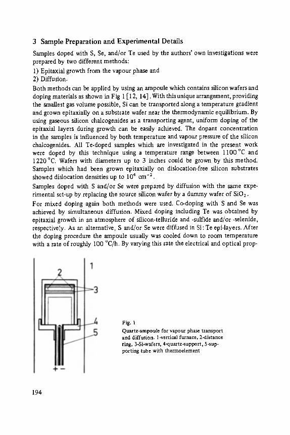
3 Sample Prepara t ion and Expe r imen ta l Details
Samples doped with S, Se, and/or Te used by the authors' own investigations were prepared by two different methods:
1) Epitaxial growth from the vapour phase and 2) Diffusion.
Both methods can be applied by using an ampoule which contains silicon wafers and doping materials as shown in Fig 1 [ 12, 14]. With this unique arrangement, providing the smallest gas volume possible, Si can be transported along a temperature gradient and grown epitaxiaUy on a substrate wafer near the thermodynamic equilibrium. By using gaseous silicon chalcogenides as a transporting agent, uniform doping of the epitaxial layers during growth can be easily achieved. The dopant concentration in the samples is influenced by both temperature and vapour pressure of the silicon chalcogenides. All Te-doped samples which are investigated in the present work were doped by this technique using a temperature range between 1100 ~ and 1220 ~ Wafers with diameters up to 3 inches could be grown by this method. Samples which had been grown epitaxially on dislocation-free silicon substrates showed dislocation densities up to 104 cm -2 .
Samples doped with S and/or Se were prepared by diffusion with the same expe- rimental set-up by replacing the source silicon wafer by a dummy wafer of SiO:.
For mixed doping again both methods were used. Co-doping with S and Se was achieved by simultaneous diffusion. Mixed doping including Te was obtained by epitaxial growth in an atmosphere of silicon-telluride and -sulfide and/or -selenide, respectively. As an alternative, S and/or Se were diffused in Si: Te epi-layers. After the doping procedure the ampoule usually was cooled down to room temperature with a rate of roughly 100 ~ By varying this rate the electrical and optical prop-
Fig. 1 Quartz-ampoule for vapour phase transport and diffusion. 1-vertical furnace, 2-distance ring, 3-Si-wafers, 4-quartz-support, 5-sup- porting tube with thermoelement
194
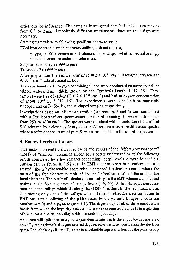
erties can be influenced. The samples investigated here had thicknesses ranging from 0.5 to 2 mm. Accordingly diffusion or transport times up to 14 days were necessary.
Starting materials with following specifications were used:
FZ-silicon electronic grade, monocrystalline, dislocation-free,
p-type, ~ 1000 ohmcm or ~ 1 ohmcm, depending on whether neutral or singly ionized donors are under consideration.
Sulphur, Selenium: 99.999 % pure Tellurium: 99.9999 % pure.
After preparation the samples contained ~ 2 • 1017 cm -3 interstitial oxygen and ~< 1016 cm -3 substitutional carbon.
The experiments with oxygen containing silicon were conducted on monocrystalline silicon wafers, 2 m m thick, grown by the Czochralski-method [17, 18]. These samples were free of carbon (C < 5 • 10 is cm -3) and had an oxygen concentration of about 1018 cm -3 [15, 16]. The experiments were done both on nominally undoped and on P-, Sb-, B-, and Al-doped samples, respectively.
Investigations based on infrared-absorption (see sections 5 and 6) were carried out with a Fourier-transform spectrometer capable of scanning the wavenumber range from 250 to 4800 cm -~ . The spectra were obtained with a resolution of 1 cm -1 at 8 K achieved by a closed cycle cryo-cooler. All spectra shown are difference spectra where a reference spectrum of pure Si was subtracted from the sample's spectrum.
4 Energy Levels o f Donors
This section presents a short review of the results of the "effective-mass-theory" (EMT) of "shallow" donors in silicon for a better understanding of the following results completed by a few remarks concerning "deep" levels. A more detailed dis- cussion can be found in [19] e.g.. In EMT a donor-center in a semiconductor is treated like a hydrogen-like atom with a screened Coulomb-potential where the mass of the free electron is replaced by the "effective mass" of the conduction band electrons. The result of calculations according to the EMT-scheme is amodified hydrogen-like Rydberg-series of energy levels [19, 20]. Si has six equivalent con- duction band valleys which lie along the (100)-directions in the reciprocal space. Considering only one of the valleys with anisotropic effective electron masses in EMT one gets a splitting of the p-like states into a po-state (magnetic quantum number m = 0) and a p• (m = -+ 1). The degeneracy of all of the 6 conduction bands from which the impurity's electronic states are constructed leads to a splitting of the s-states due to the valley-orbit interaction [19, 21] :
An s-state will split into an A1-state (not degenerate), an E-state (doubly degenerate), and a T2-state (threefold degenerate, all degeneracies without considering the electron spin). The labels A1, E, and T: refer to irreducible representations of the point group
195
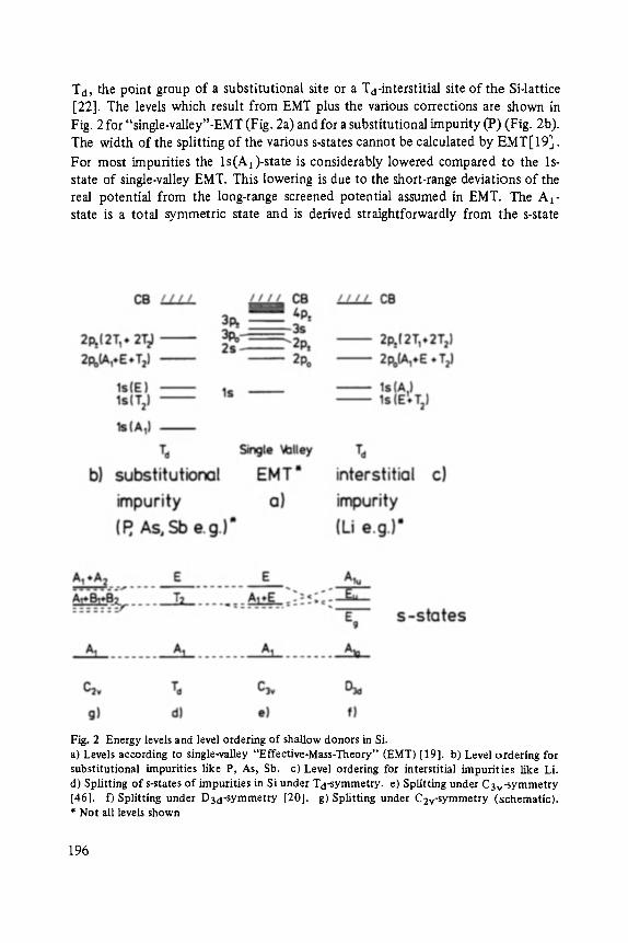
Td, the point group of a substitutional site or a Td-interstitial site of the Si-lattice [22]. The levels which result from EMT plus the various corrections are shown in Fig. 2 for "single-valley"-EMT (Fig. 2a) and for a substitutional impurity (P) (Fig. 2b). The width of the splitting of the various s-states cannot be calculated by EMT[19] .
For most impurities the ls(A1)-state is considerably lowered compared to the Is- state of single-valley EMT. This lowering is due to the short-range deviations of the real potential from the long-range screened potential assumed in EMT. The A1- state is a total symmetric state and is derived straightforwardly from the s-state
Fig. 2 Energy levels and level ordering of shallow donors in Si. a) Levels according to single-valley "Effective-Mass-Theory" (EMT) [19]. b) Level ordering for substitutional impurities like P, As, Sb. c) Level ordering for interstitial impurities like Li. d) Sphtting of s-states of impurities in Si under Td-symmetry. e) Splitting under C3v-symmetry [46]. f)Splitting under D3d-symmetry [20]. g)Splitting under C2v-symmetry (schematic). * Not all levels shown
196
under the full rotation group. As a consequence a wave-function has a high probability density at the center of the donor site, in contrast to ls(T:)- and ls(E)-states, and therefore is most sensitive to the true potential of the impurity atom. In accordance with the same argument the ls(Ta)- and ls(E)-states having nodes at the defects midpoint (p ~ T2, d ~ E + T2) show only a weak lowering compared with EMT. The amount of the lowering is characteristic for the chemical nature of the impurity and is therefore called "chemical shift" of "central cell correction". In addition to the "chemical" influence there is also an influence of the crystallographic site of the impurity on the ordering of the levels and the chemical shift. Interstitial Li or Mg, which would by no means be expected to be donors on a substitutional site, become donors if they are situated on an interstitial site with tetrahedral symmetry [23, 24, 25]. As a consequence, the ordering of the various is-levels is inverted (Fig. 2c). The excited states of the impurity having a much smaller binding energy are not or at least much weaker influenced by a short-range contribution to the potential and show, therefore, a much weaker chemical shift or splitting if at all [19, 20]. Chemical shift results from a short-range, non-Coulombic part of the potential near the defect. Such potentials give rise to "deep" levels [26, 27] and do not have a Rydberg series of excited states in contrast to "shallow" levels obeying EMT as mentioned above.
The term "deep" stems from the fact that the binding energies of such impurities (transition metals e.g.) are much higher than that of "shallow" impurities. The ground states of deep impurities no longer can be constructed from wave-functions of the lowest conduction band alone, but only under participation of other bands, the valence bands e.g.. There are different ways of calculating the energy levels of deep impurities based on LCAO-(linear combination of atomic orbitals) or pseudopotential-methods [18, 26, 27, 28, 29, 30, 31, 32], but agreement with experimental values is moderate. Most of the calculations, however, can demonstrate trends of energy levels in a series of impurities or host matrices. A semiempirical approach uses the ionization energies of the free atoms as a measure for the short- range potentials [27, 28] and predicts level energies of isolated impurities and impurity pairs that will be discussed later.
5 S-, Se-, Te-related Centers
5.1 Isolated Chalcogen Impurities
IR-absorption spectra of S-related centers in Si have been reported for the first time by [32, 33]. More detailed investigations of Si doped with S, Se, or Te have been published only recently [34, 35, 36, 37]. Due to their electronic configuration one expects substitutional chalcogens to be double donors, but by EPR (electron-paramagnetic-resonance) and ENDOR (electron-nuclear double reso- nance) investigations it could not be proved without doubt on which crystallo-
197
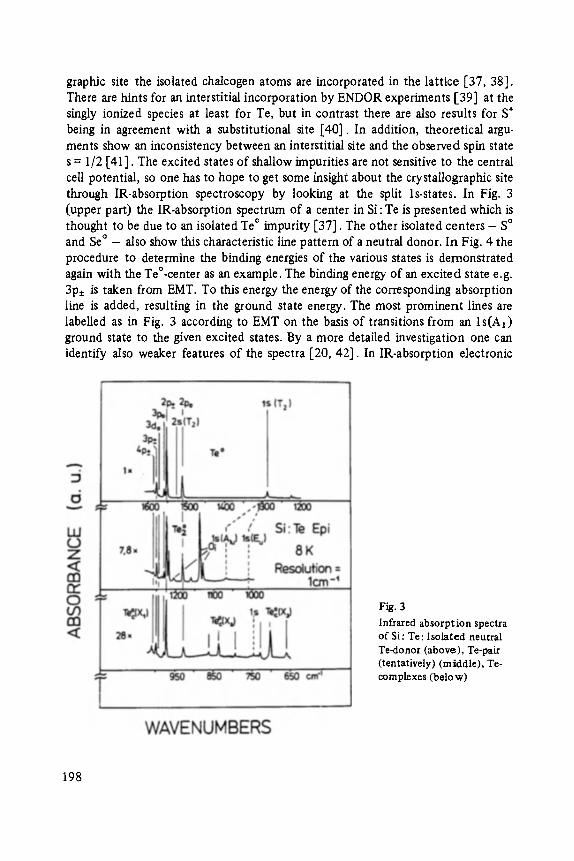
graphic site the isolated chalcogen atoms are incorporated in the lattice [37, 38]. There are hints for an interstitial incorporation by ENDOR experiments [39] at the singly ionized species at least for Te, but in contrast there are also results for S § being in agreement with a substitutional site [40]. In addition, theoretical argu- ments show an inconsistency between an interstitial site and the observed spin state s = 1/2 [41]. The excited states of shallow impurities are not sensitive to the central cell potential, so one has to hope to get some insight about the crystallographic site through IR-absorption spectroscopy by looking at the split Is-states. In Fig. 3 (upper part) the IR-absorption spectrum of a center in Si: Te is presented which is thought to be due to an isolated Te ~ impurity [37]. The other isolated centers - S ~ and Se ~ - also show this characteristic line pattern of a neutral donor. In Fig. 4 the procedure to determine the binding energies of the various states is demonstrated again with the Te~ as an example. The binding energy of an excited state e.g. 3pt is taken from EMT. To this energy the energy of the corresponding absorption line is added, resulting in the ground state energy. The most prominent lines are labelled as in Fig. 3 according to EMT on the basis of transitions from an ls(A1) ground state to the given excited states. By a more detailed investigation one can identify also weaker features of the spectra [20, 42]. In IR-absorption electronic
Fig. 3 Infrared absorption spectra of Si: Te: Isolated neutral Te-donor (above), Te-paff (tentatively) (middle), Te- complexes (below)
198
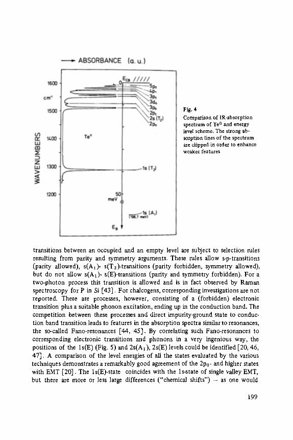
Fig. 4 Comparison of IR-absorption spectrum of Te 0 and energy level scheme. The strong ab- sorption lines of the spectrum a~e clipped in order to enhance weaker features
transitions between an occupied and an empty level are subject to selection rules resulting from parity and symmetry arguments. These rules allow s-p-transitions (parity allowed), s(A1)- s(T2)-transitions (parity forbidden, symmetry allowed), but do not allow s(Al)- s(E)-transitions (parity and symmetry forbidden). For a two-photon process this transition is allowed and is in fact observed by Raman spectroscopy for P in Si [43]. For chalcogens, corresponding investigations are not reported. There are processes, however, consisting of a (forbidden) electronic transition plus a suitable phonon excitation, ending up in the conduction band. The competition between these processes and direct impurity-ground state to conduc- tion band transition leads to features in the absorption spectra similar to resonances, the so-called Fano-resonances [44, 45]. By correlating such Fano-resonances to corresponding electronic transitions and phonons in a very ingenious way, the positions of the ls(E) (Fig. 5) and 2S(Al), 2s(E) levels could be identified [20, 46, 47]. A comparison of the level energies of all the states evaluated by the various techniques demonstrates a remarkably good agreement of the 2p0- and higher states with EMT [20]. The ls(E)-state coincides with the 1s-state of single valley EMT, but there are more or less large differences ("chemical shifts") - as one would
199
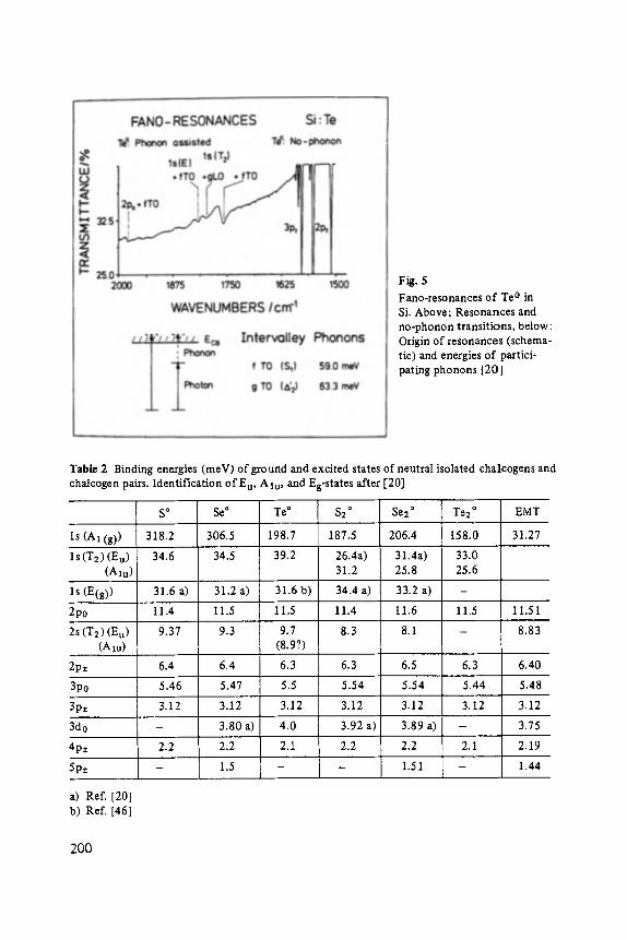
Fig. 5
Fano-resonances of Te o in Si. Above: Resonances and no-phonon transitions, below : Origin of resonances (schema- tic) and energies of partici- pating phonons [20]
Table 2 Binding energies (meV) of ground and excited states of neutral isolated chalcogens and chalcogen pairs. Identification of E u, Alu, and Eg-states after [20]
ls (At (g)) 318.2
ls(T2) (Eu) 34.6 (Alu)
ls (E(g)) 31.6 a)
2p0 11.4
2s(Tu) (Eu) 9.37 (A la)
S ~ Se ~
306.5
34.5
31.2 a)
11.5
9.3
2p• 6.4 6.4
3po 5.46 5.47
3p• 3.12 3.12
3do - 3.80 a)
4p• 2.2 2.2
5p• - 1.5
a) Ref. [201 b) Ref. [46]
We ~
198.7
39.2
31.6 b)
11.5
9.7 (8.97)
6.3
5.5
3.12
4.0
2.1
$2 ~ Se2 ~
187.5 206.4
26.4a) 31.4a) 31.2 25.8
34.4 a) 33.2 a)
11.4 11.6
8.3 8.1
6.3 6.5
5.54 5.54
3.12 3.12
3.92 a) 3.89 a)
2.2 2.2
- 1.51
Te2 ~ EMT
158.0 31.27
33.0 25.6
11.5 11.51
- 8.83
6.3 6.40
5.44 5.48
3.12 3.12
- 3.75
2.1 2.19
- 1.44
200
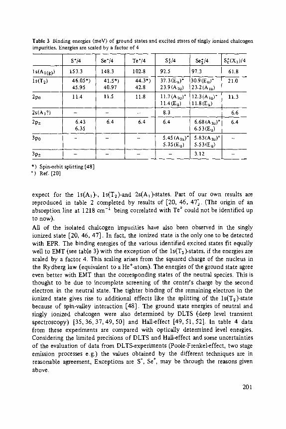
Table 3 Binding energies (meV) of ground states and excited states of singly ionized chalcogen impurities. Energies are scaled by a factor of 4
lS(Al(g))
ls(T2)
2po
S§
153.3
46.05*) 45.95
11.4
Se§
148.3
41.5") 40.97
11.5
Te+/4
102.8
44.3*) 42.8
11.8
S~/4
92.5
37.3 (Eu) § 23.9 (Am)
11.7 (A lu)* 11.4 (Eu)
Se~/4
97.3
30.9 (Eu) § 23.2(Alu)
12.3(Alu) § 11.8 (E u )
S~(XI)/4
61.8
21.0
11.3
~s(Al?) - - - 8.3 6.6
~.p• 6.43 6.4 6.4 6.4 6.68 (A1u) § 6.4 6.35 6.53 (Eu)
)po - - - 5.45 (Alu) § 5.83(Alu) § - 5.35(E u) 5.53(E u)
3p• . . . . 3.12
*) Spin-orbit spirting [48] +) Ref. [20]
expect for the ls(A1)-, ls(T2)-and 2s(A1)-states. Part of our own results are reproduced in table 2 completed by results of [20, 46, 47]. (The origin of an absorption line at 1218 cm -1 being correlated with Te ~ could not be identified up to now).
All of the isolated chalcogen impurities have also been observed in the singly ionized state [20, 46, 47]. In fact, the ionized state is the only one to be detected with EPR. The binding energies of the various identified excited states fit equally well to EMT (see table 3) with the exception of the ls(T2)-states, if the energies are scaled by a factor 4. This scaling arises from the squared charge of the nucleus in the Rydberg law (equivalent to a He+-atom). The energies of the ground state agree even better with EMT than the corresponding states of the neutral species. This is thought to be due to incomplete screening of the center's charge by the second electron in the neutral state. The tighter binding of the remaining electron in the ionized state gives rise to additional effects like the splitting of the ls(T:)-state because of spin-valley interaction [48]. The ground state energies of neutral and singly ionized chalcogen were also determined by DLTS (deep level transient spectroscopy) [35, 36, 37, 49, 50] and Hall-effect [49, 51,521. In table 4 data from these experiments are compared with optically determined level energies. Considering the limited precisions of DLTS and Hall-effect and some uncertainties of the evaluation of data from DLTS-experiments (Poole-Frenkel-effect, two stage emission processes e.g.) the values obtained by the different techniques are in reasonable agreement, Exceptions are S § Se § may be through the reasons given
above.
201
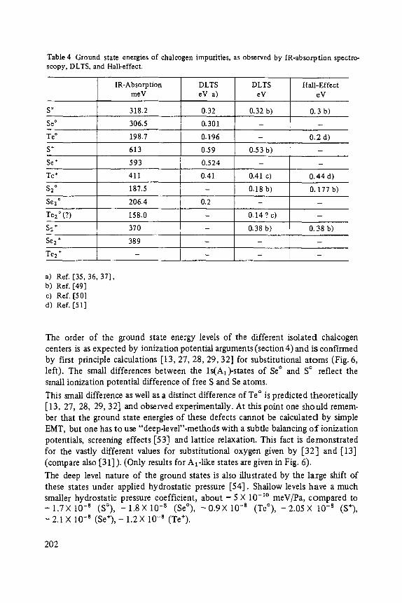
Table 4 Ground state energies of chalcogen impurities, as observed by IR-absorption spectro- scopy, DLTS, and Hall-effect.
IR-Absorption DLTS D L T S Hall-Effect meV eV a) eV eV
S ~ 318.2 0.32 0.32 b) 0.3 b)
Se ~ 306.5 0.301 - -
Te ~ 198.7 0.196 - 0.2 d)
S + 613 0.59 0.53 b) -
Se § 593 0.524 - -
Te § 411 0.41 0.41 c) 0.44 d)
$2 ~ 187.5 - 0.18 b) 0. 177 b)
Se2 ~ 206.4 0.2 - -
Te2~ (?) 158.0 - 0.14 ? c) -
S~ § 370 - 0.38 b) 0.38 b)
Se2 § 389 - - -
Te 2 ~ . . . .
a) Ref. [35, 36, 37], b) Ref. [49] c) Ref. [50] d) Ref. [51]
The order of the ground state energy levels of the different isolated chalcogen centers is as expected by ionization potential arguments (section 4) and is confirmed by first principle calculations [13, 27, 28, 29, 32] for substitutional atoms (Fig. 6, left). The small differences between the ls(A1)-states of Se ~ and S ~ reflect the small ionization potential difference of free S and Se atoms.
This small difference as well as a distinct difference of Te ~ is predicted theoretically [13, 27, 28, 29, 32] and observed experimentally. At this point one should remem- ber that the ground state energies of these defects cannot be calculated by simple EMT, but one has to use "deep-lever'-methods with a subtle balancing o f ionization
potentials, screening effects [53] and lattice relaxation. This fact is demonstrated for the vastly different values for substitutional oxygen given by [32] and [13] (compare also [31] ). (Only results for At-like states are given in Fig. 6).
The deep level nature of the ground states is also illustrated by the large shift of
these states under applied hydrostatic pressure [54]. Shallow levels have a much smaller hydrostatic pressure coefficient, about - 5 X 10 -1~ meV/Pa, compared to -1 .7X lO -s (S~ - 1 . 8 X 1 0 -s (Se~ - 0 . 9 X 1 0 -s (Te~ - 2 . 0 5 X 10 -s (S+), - 2 . 1 X 10 -8 ( S e * ) , - 1 .2X 10 - s (Te*).
202
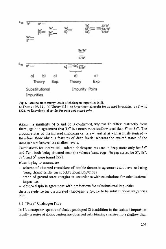
Fig. 6 Ground state energy levels of chalcogen impurities in Si. a) Theory [29, 32]. b) Theory [13]. c) Experimental results for isolated impurities, d) Theory [321- e) Experimental results for pure and mixed pairs.
Again the similarity of S and Se is confirmed, whereas Te differs distinctly from them, again in agreement that Te ~ is a much more shallow level than S ~ or Se ~ . The ground states of the isolated chalcogen centers - neutral as well as singly ionized - therefore show obvious features of deep levels, whereas the excited states of the same centers behave like shallow levels.
Calculations for interstitial, isolated chalcogens resulted in deep states only for Se ~ and Te ~ both being situated near the valence band edge. No gap states for S § Se § Te § and S ~ were found 155].
When trying to summarize
- scheme of observed transitions of double donors in agreement with level ordering being characteristic for substitutional impurities
- trend of ground state energies in accordance with calculations for substitutional impurities
- observed spin in agreement with predictions for substitutional impurities
there is evidence for the isolated chalcogens S, Se, Te to be substitutional impurities in Si.
5.2 "Pure" Chalcogen Pairs
In IR-absorption spectra of chalcogen doped Si in addition to the isolated impurities usually a series of donor centers are observed with binding energies more shallow than
203
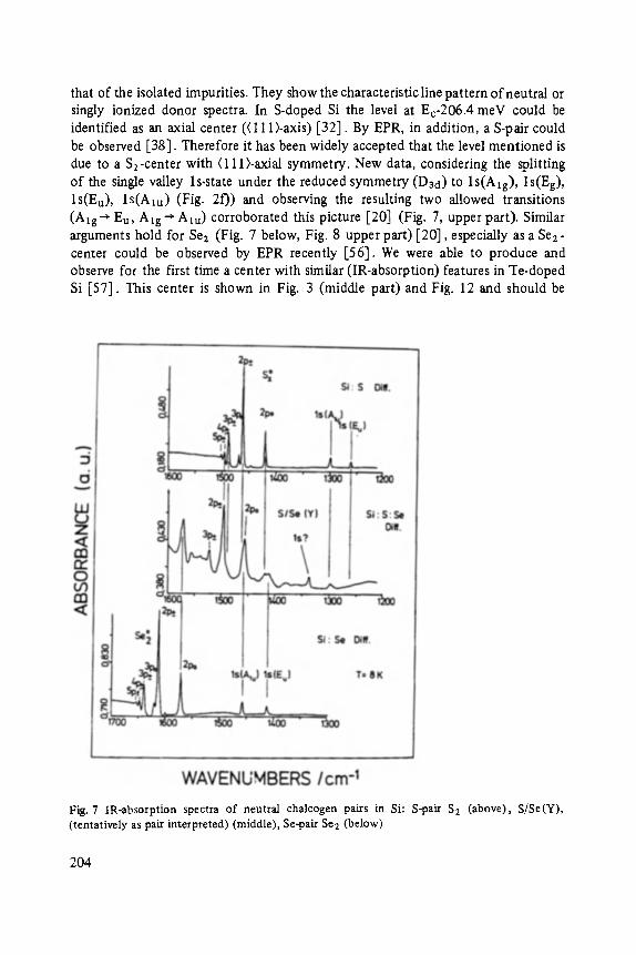
that of the isolated impurities. They show the characteristic line pattern of neutral or singly ionized donor spectra. In S-doped Si the level at Ec-206.4 meV could be identified as an axial center ((111)-axis) [32]. By EPR, in addition, a S-pair could be observed [38]. Therefore it has been widely accepted that the level mentioned is due to a S2-center with (11 l)-axial symmetry. New data, considering the splitting of the single valley ls.state under the reduced symmetry (D3d) to ls(Alg), ls(Eg), ls(Eu), ls(Alu) (Fig. 20) and observing the resulting two allowed transitions (Azg ~ Eu, Alg ~ Azu) corroborated this picture [20] (Fig. 7, upper part). Similar arguments hold for Se2 (Fig. 7 below, Fig. 8 upper part) [20], especially as a Se2- center could be observed by EPR recently [56]. We were able to produce and observe for the first time a center with similar (IR-absorption) features in Te-doped Si [57]. This center is shown in Fig. 3 (middle part) and Fig. 12 and should be
Fig. 7 IR-absorption spectra of neutral chalcogen pairs in Si: S-pair $2 (above), S/Se(Y), (tentatively as pair interpreted) (middle), Se-pair Se 2 (below)
204
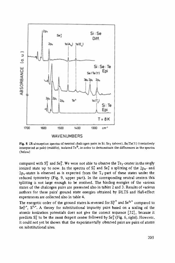
Fig. 8 IR-absorption spectra of neutral chalcogen pairs in Si: Se2 (above), Se/Te(Y) (tentatively interpreted as pair) (middle), isolated Te ~ in order to demonstrate the differences in the spectra (below)
compared with S~ and Se~. We were not able to observe the Te2-center in the singly ionized state up to now. In the spectra of S + 2 and Se~ a splitting of the 2po- and 2p• is observed as is expected from the T2-part of these states under the reduced symmetry (Fig. 9, upper part). In the corresponding neutral centers this splitting is not large enough to be resolved. The binding energies of the various states of the chalcogen pairs are presented also in tables 2 and 3. Results of various authors for these pairs' ground state energies obtained by DLTS and Hall-effect experiments are collected also in table 4.
The energetic order of the ground states is reversed for S~ + and Se ~+ compared to Se~ '§ S ~ A theory for substitutional impurity pairs based on a scaling of the atomic ionization potentials does not give the correct sequence [32], because it predicts S ~ 2 to be the most deepest center followed by Se~ (Fig. 6, right). However, it could not yet be shown that the experimentally observed pairs are pairs of atoms on substitutional sites.
205
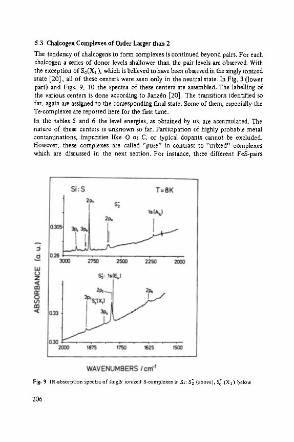
5.3 Chaleogen Complexes of Order Larger than 2
The tendency of chalcogens to form complexes is continued beyond pairs. For each chalcogen a series of donor levels shallower than the pair levels are observed. With the exception of Sc(X~), which is believed to have been observed in the singly ionized state [20], all of these centers were seen only in the neutral state. In Fig. 3 (lower part) and Figs. 9, 10 the spectra of these centers are assembled. The labelling of the various centers is done according to Janzdn [20]. The transitions identified so far, again are assigned to the corresponding final state. Some of them, especially the Te-complexes are reported here for the first time.
In the tables 5 and 6 the level energies, as obtained by us, are accumulated. The nature of these centers is unknown so far. Participation of highly probable metal contaminations, impurities like O or C, or typical dopants cannot be excluded. However, these complexes are called "pure" in contrast to "mixed" complexes which are discussed in the next section. For instance, three different FeS-pairs
4" Fig. 9 IR-absorption spectra of singly ionized S-complexes in Si: S~ (above), S c (X l) below
206
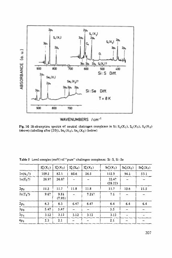
Fig. 10 IR-absorption spectra of neutral chalcogen complexes in Si: Sc(XI), Sc(X3), Sc(X 5) (above) (labelling after [201), Sec(XD, See(X2) (below)
Table 5 Level energies (meV) of " p ~ e " chalcogen complexes: Si : S, Si : Se
Is(At?)
ls(T2?)
2po
~s (T2 ?)
~po 3'p• ,p•
s ~ ( x l ) s~(x3) s~(x4)
109,5 82,1 80.6
26.9? 26.8? -
11.5 11.7 11.8
9.6? 9.81 - (7.95)
6.3 6.3 6.47
5.47 5.47 -
3.12 3.12 3.12
2.3 2.1 -
s ; (Xs ) Se~(Xx)
56.5 115.9
- 32.4? (28.22)
11.8 11.7
7.217 7.1
6.47 6.4
- 5,5
3.12 3.12
- 2 , 1
Se~(X2)
94.1
10.6
6.4
Se~(X3)
53.1
11.5
6.4
207

[38] have been reported. SeB-pairs suggested by [52] probably were Se2-centers.
In tent ional co-doping with metals and one chalcogen did not enhance the absorp-
t ion lines o f the complexes, nor were obta ined addit ional new centers provided
sample t rea tment was as described and the samples were slowly cooled af ter high-
Table 6 Level energies (meV) of"pure" chalcogen complexes: Si: Te
Te~(X1) Te~(X2) Te~(X3) Te~(X4) Te~(Xs)
ls(Al?) 126.8 109,8 93.3 73,1 65.3
37,4? ls(T2?) 34.4 - 35.5? 29.8 -
29.6
2po 11.9 11.5 11.5 11.4 12.3
9.4? 2s(T27) . . . . 7.45?
2p• 6.5 6.3 6.2 6.3 6.5
3po 5.6 - 5.5 5.6 5.7
3.12 3.12 3.12 3.12 3.12 3p•
4p+ 2.1 - - - 2.4?
Fig. 11 Concentrations of various chalcogen centers in Si. Shown are schematically the heights of the absorption lines of the 2p• and 2p0-transitions. Different scales of the abszissa are used for the different elements
208
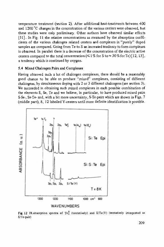
temperature treatment (section 2). After additional heat-treatments between 400 and 1200 ~ changes in the concentration of the various centers were observed, but these studies were only preliminary. Other authors have observed similar effects [51]. In Fig. 11 the relative concentrations as measured by the absorption coeffi- cients of the various chalcogen related centers and complexes in "purely" doped samples are compared. Going from Te to S an increased tendency to form complexes is observed. In parallel there is a decrease of the concentration of the electric active centers compared to the total cencentration (<~ 1% for S to ~ 30 % fo r t e ) [12, 13], a tendency which is continued by oxygen.
5.4 Mixed Chalcogen Pairs and Complexes
Having observed such a lot of chalcogen complexes, there should be a reasonably good chance to be able to produce "mixed" complexes, consisting of different chalcogens, by simultaneous doping with 2 or 3 different chalcogens (see section 3). We succeeded in obtaining such mixed complexes in each possible combination of the elements S, Se, Te and we believe, in particular, to have produced mixed pairs S-Se-, Se-Te- and, with a bit more uncertainty, S-Te-pairs which are shown in Figs. 7 (middle part), 8, 12 labelled Y-centers until more definite identification is possible.
Fig. 12 IR-absorption spectra of Te ~ (tentatively) and S/Te(Y) (tentatively interpreted as S/Te-pair)
2O9
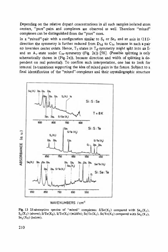
Depending on the relative dopant concentrations in all such samples isolated atom centers, "pure"-pairs and complexes are observed as well. Therefore "mixed" complexes can be distinguished from the "pure" ones.
In a "mixed"-pair with a configuration similar to $2 or Se2 and an axis in (111)- direction the symmetry is further reduced from D3d to C3v because in such a pair no inversion center exists. Hence, T2-states in Td-symmetry might split into an E- and an Al-state under C3v-symmetry (Fig. 2e)) [58]. (Possible splitting is only schematically shown in (Fig. 2e)), because direction and width of splitting is de- pendent on real potential). To confirm such interpretation, one has to look for internal 1 s-transitions supporting the idea of mixed pairs in the future. Subject to a final identification of the "mixed"-complexes and their crystallographic structure
Fig. 13 IR-absorption spectra of "mixed" complexes: S/Se(X1) compared with See(X1), Se(X1) (above); S/Te(X2), S/Te(X3) (middle); Se/Te(X1), Se/Te(X2) compared with See(X1) , Sec(X 2) (below).
210
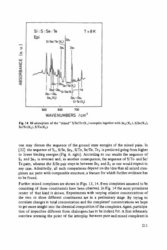
Fig. 14 IR-absorption of the "mixed" S/Se/Te(Xi)-complex together with Sec(X t), S/Se(Xt), Se/Te(X2), S/Te(X 2)
one may discuss the sequence of the ground state energies of the mixed pairs. In [32] the sequence of $2, S/Se, Se2, S/Te, Se/Te, Te2 is predicted going from higher to lower binding energies (Fig. 6, right). According to our results the sequence of $2 and Se2 is reversed and, as another consequence, the sequence of S/Te- and Se/ Te-pairs, whereas the S/Se-pair stays in between Se2 and $2 as one would expect in any case. Admittedly, all such comparisons depend on the idea that all mixed com- plexes are pairs with comparable structure, a feature for which further evidence has to be found.
Further mixed complexes are shown in Figs. 13, 14. Even complexes assumed to be consisting of three constituents have been observed. In Fig. 14 the most prominent center of that kind is shown. Experiments with varying relative concentrations of the two or three different constituents are in a preliminary stage. By trying to correlate changes in total concentration and the complexes' concentrations we hope to get more insight into the chemical composition of the complexes. Again, participa- tion of impurities different from chalcogens has to be looked for. A first schematic overview stressing the point of the interplay between pure and mixed complexes is
211
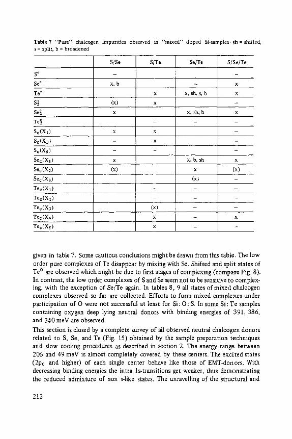
T a b l e 7 " P u r e " c h a l c o g e n i m p u r i t i e s o b s e r v e d in " m i x e d " d o p e d S i - s a r n p l c s - s h = sh i f ted ,
s = spli t , b = b r o a d e n e d
S/Se S/Te Se/Te S / S e / T e
S ~ _ _ - -
Se ~ x, b - x
Te ~ x x, sh, s, b x
S~ (x) x -
Se~ x x, sh, b x
T e ~ . . . .
So(X1) x x -
Sc(X3) - x -
Sc(Xs) - - -
Sec(X D x x, b, sh x
Sec(X2) (x) x (x)
S e c ( X 3 ) (x) -
Tec(Xt) . . . .
Tec(X2) - - -
I ' e c ( X 3 ) (x) - -
Tec(X4) x - x
Tec(Xs) x - -
given in table 7. Some cautious conclusions might be drawn from this table. The low order pure complexes of Te disappear by mixing with Se. Shifted and split states of Te ~ are observed which might be due to first stages of complexing (compare Fig. 8). In contrast, the low order complexes of S and Se seem not to be sensitive to complex- ing, with the exception of Se/Te again. In tables 8, 9 all states of mixed chalcogen complexes observed so far are collected. Efforts to form mixed complexes under participation of O were not successful at least for Si: O: S. In some Si: Te samples containing oxygen deep lying neutral donors with binding energies of 391 ,386 , and 340 meV are observed.
This section is closed by a complete survey of all observed neutral chalcogen donors related to S, Se, and Te (Fig. 15) obtained by the sample preparation techniques and slow cooling procedures as described in section 2. The energy range between 206 and 49 meV is almost completely covered by these centers. The excited states (2p0 and higher) of each single center behave like those of EMT-donors. With decreasing binding energies the intra Is-transitions get weaker, thus demonstrating the reduced admixture of non s-like states. The unravelling of the structural and
212
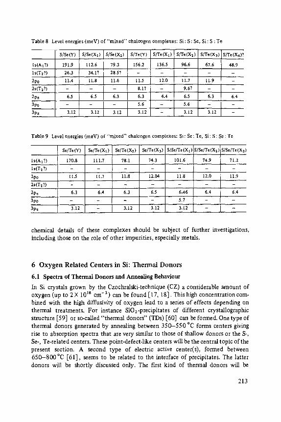
Tab le 8 Level energies (meV) o f " m i x e d " cha tcogen complexes : Si: S : Se, Si : S : Te
t s (Al?)
l s (Tl? )
2 p o
2s(Ts?)
2p•
3 p o
3p•
S/Se(Y) S/Se(Xl) S/Se(X2) SITe(Y) S/Te(XI) S/Te(Xs) S/Te(X3)
191.9 112.6 79.3 156.2 136.5 96.6 67.6
26,3 34.17 28.5? . . . .
11'.4 11.8 11.6 11,5 12.0 11.7 11.9
- - - 8.17 - 9.67 -
6.5 6.5 6.3 6,3 6.4 6.5 6.3
- - - 5 . 6 - 5 . 6 -
3 . 1 2 3.12 3.12 3,12 - 3.12 3.12
SITe (X4)?
48.9
w
6,4
Tab le 9 Level energies (meV) of " m i x e d " cha lcogen complexes : Si : Se : Te, Si : S : Se : Te
Se/Te (Y)
Is(At?) 170.8
Is(Ts? )
2po 11.5
2s(Ts? )
2p• 6.3
3po
3p• 3.12
Se/Te(Xl) Se/Te (Xz)
111.7 78.1
11.7 11.8
6.4 6.3
- 3.12
Se/Te (X3) : S/Se/Te (Xl)
74.3 101.6
- - N
12.04 11.8
6.5 6.46
- 5.7
3.12 3.12
S/Se/Te(Xs) S/Se/Te (X3)
74.9 71.2
12.0 11.9
6.4 6.4
chemical details of these complexes should be subject of further investigations, including those on the role of other impurities, especially metals.
6 Oxyge n Rela ted Centers in Si: Thermal Donors
6.1 Spectra of Thermal Donors and Annealing Behaviour
In Si crystals grown by the Czochralski-technique (CZ) a considerable amount of oxygen (up to 2 X 10 is cm -3) can be found [17, 18]. This high concentration com- bined with the high diffusivity of oxygen lead to a series of effects depending on thermal treatments. For instance SiOs-precipitates of different crystallographic structure [59] or so-called "thermal donors" (TDs) [60] can be formed. One type of thermal donors generated by annealing between 350-550 ~ forms centers giving rise to absorption spectra that are very similar to those of shallow donors or the S-, Se-, Te-related centers. These point-defect-like centers will be the central topic of the present section. A second type of electric active center(s), formed between 650--800~ [61], seems to be related to the interface of precipitates. The latter donors will be shortly discussed only. The first kind of thermal donors will be
213
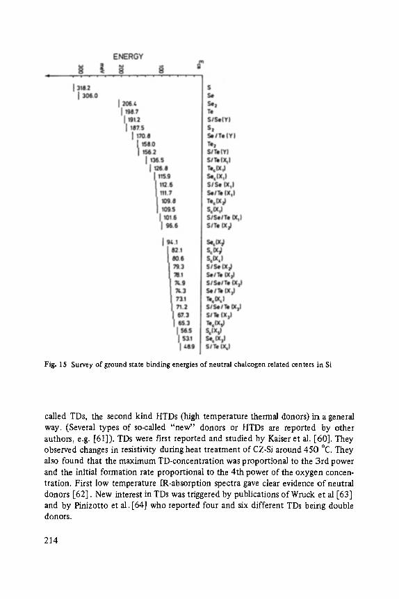
Fig. 15 Survey of ground state binding energies of neutral chalcogen related centers in Si
called TDs, the second kind HTDs (high temperature thermal donors) in a general way. (Several types of so-called "new" donors or HTDs are reported by other authors, e.g. [61]). TDs were first reported and studied by Kaiser et al. [60]. They observed changes in resistivity during heat treatment of CZ-Si around 450 ~ They also found that the maximum TD-concentration was proportional to the 3rd power and the initial formation rate proportional to the 4th power of the oxygen concen- tration. First low temperature IR-absorption spectra gave clear evidence of neutral donors 162]. New interest in TDs was triggered by publications of Wruck et al [63] and by Pinizotto et al. [64] who reported four and six different TDs being double donors.
214
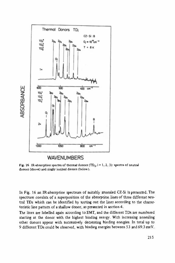
Fig. 16 IR-absorption spectra of thermal donors (TD i, i = I, 2, 3): spectra of neutral donors (above) and singly ionized donors (below).
In Fig. 16 an IR-absorption spectrum of suitably annealed CZ-Si is presented. The spectrum consists of a superposition of the absorption lines of three different new tral TDs which can be identified by sorting out the lines according to the charac- teristic line pattern of a shallow donor, as presented in section 4.
The lines are labelled again according to EMT, and the different TDs are numbered starting at the donor with the highest binding energy. With increasing annealing other donors appear with successively decreasing binding energies. In total up to 9 different TDs could be observed, with binding energies between 53 and 69.3 meV.
215

Table 10 Energies of IR-absorption lines at T = 8 K and optical binding energies E B derived from there. For TD~, E B was determined using the 3p• or, alternatively, the 2p• For TDi* the most shallow 2p• was used.
TI)-Nr.
rD~-transitions/cm- 1
2p0
2p•
3p0
3p•
EB/meV
rD~-transitions/cm -1
2po
2p•
3p•
4p•
EB/meV
1 2 3 4 5 6 7 8 9
461 442 423 405 388 372 357 343 330
507 488 470 451 434 417 404 385 376
- 494 475 456 441 . . . .
533 514 496 477 - 443 - - -
69.3 66.9 64.7 62.3 60.2 58.1 56.5 54.1 53.0
854 806 762 713 678 645
1044 991 945 889 846 (804) 1048 998 951 904 862 825
1156 1105 1057 1011 968 - 1160 1107 1059 1014 972 -
1187 . . . . I 156.3 149.7[ 143.8 138.2 132.5 127.9
1
(614) (584)
(782) (793) (769)
I
The energies of their ground states and excited states are given in table 10. Six of these donors also could be observed in the singly ionized state [65, 66-] (compare also table 10). An example of a corresponding spectrum is shown also in Fig. 16 for 3 different TDs. Compared to the neutral donors the 2p• and 3p• are split. The splitting increases with decreasing binding energies from 5 to 16 cm -1 (2p• lines) and 2 to 3.5 cm -1 (3p• respectively. Similar behaviour under thermal treatment of neutral and singly ionized TD-spectra made a correlation of TD ~ TD § spectra, and donor number possible. The energies of the various excited and ground states observed are also repeated in table 10. They are completely independent of the dopant (P, Sb, B, A1). Defects with binding energies comparable to the ones reported in table 10 have been observed in CZ-Si with DLTS and Hall-effect also [67, 68, 69], without being able to resolve the small differences in binding ener- gies between the various donors. But with Hall-effect [67] decreasing binding energies with increasing annealing time were observed. In fact binding energies as low as 18 meV are reported, so the nine TDs reported by us might not be the complete set of different TDs.
The binding energies of the various states now can again be compared with EMT (Fig. 17). The level energies of TD+ are scaled again by a factor 4 in order to correct for
216
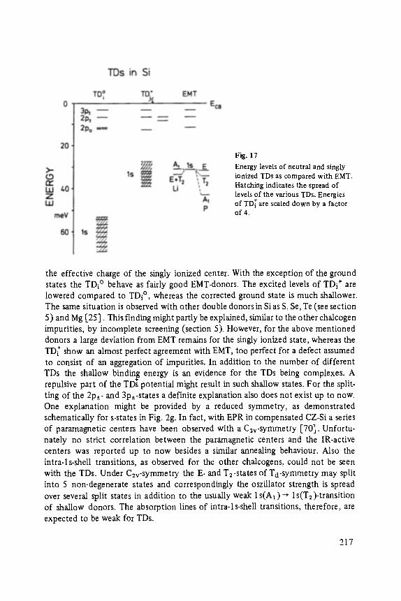
Fig. 17 Energy levels of neutral and singly ionized TDs as compared with EMT. Hatching indicates the spread of levels of the various TDs. Energies of TD~ are scaled down by a factor of 4.
the effective charge of the singly ionized center. With the exception of the ground states the TDi ~ behave as fairly good EMT-donors. The excited levels of TDi § are lowered compared to TDi ~ whereas the corrected ground state is much shallower. The same situation is observed with other double donors in Si as S, Se, Te (see section 5) and Mg [253 . This finding might partly be explained, similar to the other chalcogen impurities, by incomplete screening (section 5). However, for the above mentioned donors a large deviation from EMT remains for the singly ionized state, whereas the TD~ show an almost perfect agreement with EMT, too perfect for a defect assumed to consist of an aggregation of impurities. In addition to the number of different TDs the shallow binding energy is an evidence for the TDs being complexes. A repulsive part of the TD~ potential might result in such shallow states. For the split- ting of the 2p• and 3p._-states a definite explanation also does not exist up to now. One explanation might be provided by a reduced symmetry, as demonstrated schematically for s-states in Fig. 2g. In fact, with EPR in compensated CZ-Si a series of paramagnetic centers have been observed with a C2v-symmetry [70]. Unfortu- nately no strict correlation between the paramagnetic centers and the IR-active centers was reported up to now besides a similar annealing behaviour. Also the intra-ls-shell transitions, as observed for the other chalcogens, could not be seen with the TDs. Under C2v-symmetry the E- and T2-states of Td-symmetry may split into 5 non-degenerate states and correspondingly the oszillator strength is spread over several split states in addition to the usually weak 1 s (A~)~ l s(Tz)-transition of shallow donors. The absorption lines of intra-ls-shell transitions, therefore, are expected to be weak for TDs.
217

The absorption lines now can be used to follow the formation of the various TDs, if undoped CZ-Si is used. In Fig. 18 the result of such an experiment is shown for annealing at 460 ~ after a TD-quenching treatment at 770 ~ The concentrat ions of the TDs are measured by the absorption coefficients ~i of the 2po-transitions, neglecting minor changes of the half-width of the absorption lines. In Fig. 19 the corresponding total TD-concentration NTD as moni tored by the resistivity is plot ted as a function of annealing time. For the evaluation of NTD it was assumed that the TDs are double donors as demonstrated above and that the mobili ty at room tempera- ture does not depend on TD concentrat ion [67] . The curves for a compensated sample (#9 ) with the same O-concentration and for an undoped sample (#5.3) with half of the O-concentration are also shown in Fig. 19. According to Fig. 18 the various TDi are obviously formed with different rates and after having reached a maximum con- centration they start to decay again. By annealing at higher temperatures this be- haviour is observed even more clearly. For a total oxygen concentration of 10 TM cm -3
Fig. 18 Absorption coefficients of the 2po-transitions as a function of annealing time at 460 ~ for TD ~ i = i - 6 ; Equivalent samples ([Oi] = 1018 cm -3) were used for different time ranges: #3.2: t = 30 min - 5 h, #3.1: t > 5 h, a third sample (not indicated) was used for t < 30 min.
218
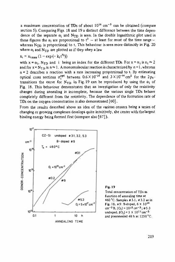
a maximum concentration of TDs of about 1016 cm -3 can be obtained (compare section 5). Comparing Figs. 18 and 19 a distinct difference between the time depen- dence of the separate a i and NTD is seen. In the double logarithmic plot used in these figures the ai are proportional to t 2 - at least for most of the time range - whereas NTD is proportional to t. This behaviour is seen more distinctly in Fig. 20 where ai and NTD are plotted as if they obey a law
Xi = Xi max (1 - exp ( - k i tn i ) )
with x = ai, NTD and i being an index for the different TDs. For x = ~i is n i ~ 2 and for x = NTD is n ~ 1. A monomolecular reaction is characterized by n = 1, whereas n = 2 describes a reaction with a rate increasing proportional to t. By estimating optical cross sections o~ pt between 0.6 X 10 -14 and 3 • 10 -~4 cmz for the 2po- transitions the curve for NTD in Fig. 19 can be reproduced by using the ai of Fig. 18. This behaviour demonstrates that an investigation of only the resistivity changes during annealing is incomplete, because the various single TDs behave completely different from the resistivity. The dependence of the formation rate of TDs on the oxygen concentration is also demonstrated [60].
From the results described above an idea of the various centers being a series of changing or growing complexes develops quite intuitively, the center with the largest binding energy being formed first (compare also [67]).
Fig. 19 Total concentrat ion of TDs as funct ion of annealing t ime at 460 ~ Samples #3 .1 , #3 .2 as in Fig. 18, # 9 : B-doped, 6 X 1014 cm -a B, [Oil = 10 t8 crn -3 ; #5 .3 undoped, [Oi] = 5 X 1017cm -3 and prearmealed 48 h at 1250 ~
219
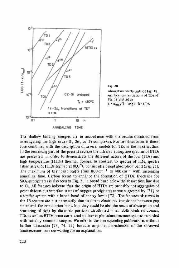
Fig. 20 Absorption coefficients of Fig. 18 and total concentrations of TDs of Fig. 19 plotted as x = Xmax(1 - exp(- k �9 tn)).
The shallow binding energies are in accordance with the results obtained from investigating the high order S-, Se-, or Te-complexes. Further discussion is there- fore combined with the description of several models for TDs in the next section. In the remaining part of the present section the infrared absorption spectra of HTDs are presented, in order to demonstrate the different nature of the low (TDs) and high temperature (HTDs) thermal donors. In contrast to spectra of TDs, spectra taken at 8K of HTDs formed at 800 ~ consist of a broad absorption band (Fig. 21). The maximum of that band shifts from 800cm -1 to 400cm -t with increasing annealing time. Carbon seems to enhance the formation of HTDs. Evidence for SiQ-precipitates is also seen in Fig. 21 : a broad band below the absorption line due to Oi. All features indicate that the origin of HTDs are probably not aggregates of point defects but interface states of oxygen precipitates as was suggested by [71] or a similar system with a broad band of energy levels [72]. The features observed in the IR-spectra are not necessarily due to direct electronic transitions between gap states and the conduction band but they could be also the result of absorption and scattering of light by dielectric particles distributed in Si. Both kinds o f donors, TDs as well as HTDs, were correlated to lines in photoluminescence spectra recorded with suitably annealed samples. We refer to the corresponding publications without further discussion [73, 74, 75] because origin and mechanism of the observed luminescence lines are waiting for an explanation.
220
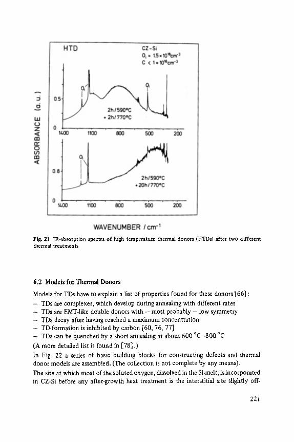
Fig. 21 IR-absorption spectra of high temperature thermal donors (HTDs) after two different thermal treatments
6.2 Models for Thermal Donors
Models for TDs have to explain a list of properties found for these donors [66] :
- TDs are complexes, which develop during annealing with different rates - TDs are EMT-like double donors with - most probably - low symmetry - TDs decay after having reached a maximum concentration - TD-formation is inhibited by carbon [60, 76, 77] - TDs can be quenched by a short annealing at about 600 ~ ~
(A more detailed list is found in [78] .)
In Fig. 22 a series of basic building blocks for constructing defects and thermal donor models are assembled. (The collection is not complete by any means).
The site at which most of the soluted oxygen, dissolved in the Si-melt, is incorporated in CZ-Si before any after-growth heat treatment is the interstitial site slightly off-
221
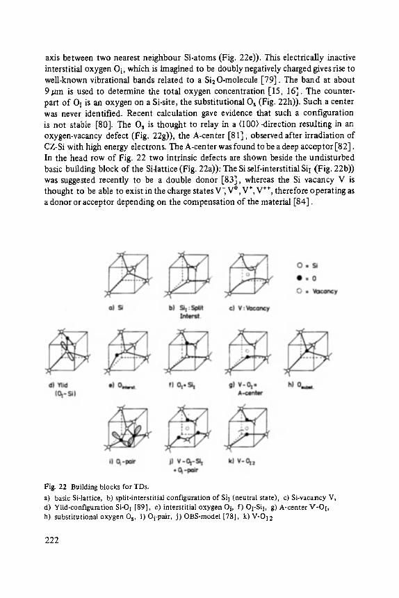
axis between two nearest neighbour Si-atoms (Fig. 22e)). This electrically inactive interstitial oxygen Oi, which is imagined to be doubly negatively charged gives rise to well-known vibrational bands related to a Si20-molecule [79]. The band at about 9/~m is used to determine the total oxygen concentration [15, 16]. The counter- part of Oi is an oxygen on a Si-site, the substitutional Os (Fig. 22h)). Such a center was never identified. Recent calculation gave evidence that such a configuration is not stable [80]. The Os is thought to relay in a (100}-direction resulting in an oxygen-vacancy defect (Fig. 22g)), the A-center [8 I ] , observed after irradiation of CZ-Si with high energy electrons. The A-center was found to be a deep acceptor [82]. In the head row of Fig. 22 two intrinsic defects are shown beside the undisturbed basic building block of the Si-lattice (Fig. 22a)): The Si self-interstitial Sii (Fig. 22b)) was suggested recently to be a double donor [83], whereas the Si vacancy V is thought to be able to exist in the charge states V , V ~ V § V §247 therefore operating as a donor or acceptor depending on the compensation of the material [84].
Fig. 22 Building blocks for TDs. a) basic Si-lattice, b) split-interstitial configuration of Si I (neutral state), c) Si-vacancy V, d) Ylid-configuration Si-O I [89], e) interstitial oxygen O i, f) OI-Si I, g) A-center V'-O I, h) substitutional oxygen O s, i) Oi-pair, j) OBS-model [78], k) V-Of2
222
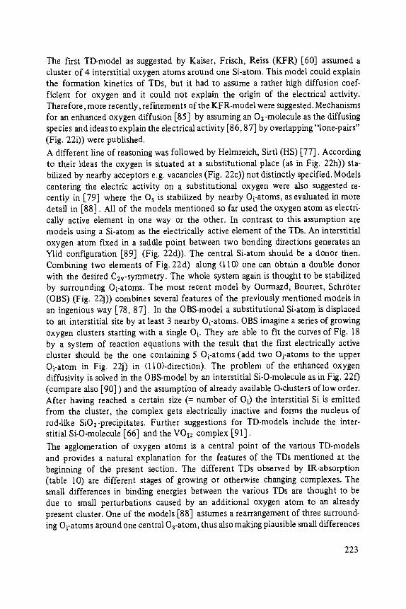
The first TD-model as suggested by Kaiser, Frisch, Reiss (KFR) [60] assumed a cluster of 4 interstitial oxygen atoms around one Si-atom. This model could explain the formation kinetics of TDs, but it had to assume a rather high diffusion coef- ficient for oxygen and it could not explain the origin of the electrical activity. Therefore, more recently, refinements of the KFR-model were suggested. Mechanisms for an enhanced oxygen diffusion [85] by assuming an 02-molecule as the diffusing species and ideas to explain the electrical activity [86, 87] by overlapping "lone-pairs" (Fig. 22i)) were published.
A different line of reasoning was followed by Helmreich, Sirtl (HS) [77]. According to their ideas the oxygen is situated at a substitutional place (as in Fig. 22h)) sta- bilized by nearby acceptors e.g. vacancies (Fig. 22c)) not distinctly specified. Models centering the electric activity on a substitutional oxygen were also suggested re- cently in [79] where the Os is stabilized by nearby Oi-atoms, as evaluated in more detail in [881. All of the models mentioned so far used the oxygen atom as electri- cally active element in one way or the other. In contrast to this assumption are models using a Si-atom as the electrically active element of the TDs. An interstitial oxygen atom fixed in a saddle point between two bonding directions generates an Ylid configuration [89] (Fig. 22d)). The central Si-atom should be a donor then. Combining two elements of Fig. 22d) along (110) one can obtain a double donor with the desired C2v-symmetry. The whole system again is thought to be stabilized by surrounding Oi-atoms. The most recent model by Ourmazd, Bourret, Schr6ter (OBS) (Fig. 22j)) combines several features of the previously mentioned models in an ingenious way [78, 87]. In the OBS-model a substitutional Si-atom is displaced to an interstitial site by at least 3 nearby Oi-atoms. OBS imagine a series of growing oxygen clusters starting with a single Oi. They are able to fit the curves of Fig. 18 by a system of reaction equations with the result that the first electrically active cluster should be the one containing 5 Oi-atoms (add two Oi-atoms to the upper Oi-atom in Fig. 22j) in (ll0)-direction). The problem of the enhanced oxygen diffusivity is solved in the OBS-model by an interstitial Si-O-molecule as in Fig. 22f) (compare also [90] ) and the assumption of already available O-chisters of low order. After having reached a certain size (= number of Oi) the interstitial Si is emitted from the cluster, the complex gets electrically inactive and forms the nucleus of rod-like SiO2-precipitates. Further suggestions for TD-models include the inter- stitial Si-O-molecule [66] and the VOI2 complex [91].
The agglomeration of oxygen atoms is a central point of the various TD-models and provides a natural explanation for the features of the TDs mentioned at the beginning of the present section. The different TDs observed by IR-absorption (table I0) are different stages of growing or otherwise changing complexes. The small differences in binding energies between the various TDs are thought to be due to small perturbations caused by an additional oxygen atom to an already present cluster. One of the models [88] assumes a rearrangement of three surround- ing Oi-atoms around one central Os-atom, thus also making plausible small differences
223
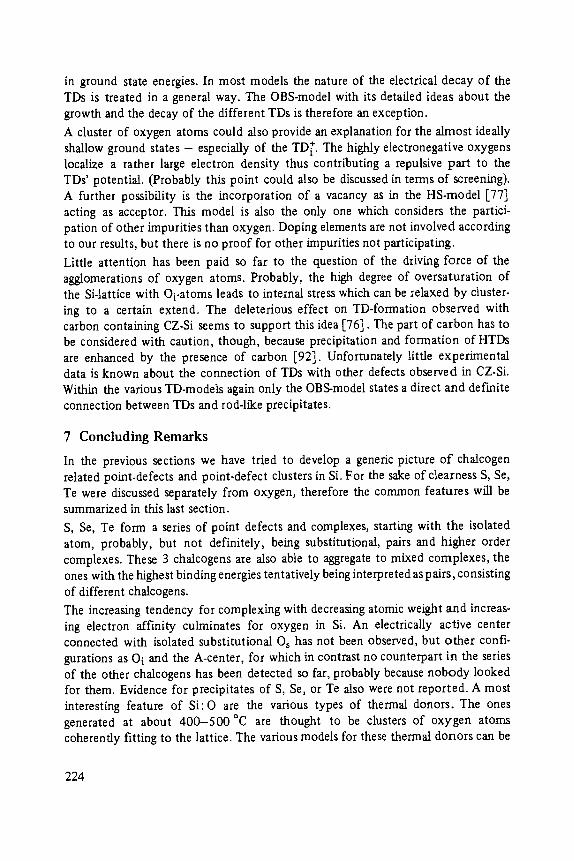
in ground state energies. In most models the nature of the electrical decay of the TDs is treated in a general way. The OBS-model with its detailed ideas about the growth and the decay of the different TDs is therefore an exception.
A cluster of oxygen atoms could also provide an explanation for the almost ideally shallow ground states - especially of the TD~. The highly electronegative oxygens localize a rather large electron density thus contributing a repulsive part to the TDs' potential. (Probably this point could also be discussed in terms of screening). A further possibility is the incorporation of a vacancy as in the HS-model [77] acting as acceptor. This model is also the only one which considers the partici- pation of other impurities than oxygen. Doping elements are not involved according to our results, but there is no proof for other impurities not participating.
Little attention has been paid so far to the question of the driving force of the agglomerations of oxygen atoms. Probably, the high degree of oversaturation of the Si-lattice with Oi-atoms leads to internal stress which can be relaxed by cluster- ing to a certain extend. The deleterious effect on TD-formation observed with carbon containing CZ-Si seems to support this idea [76]. The part of carbon has to be considered with caution, though, because precipitation and formation of HTDs are enhanced by the presence of carbon [92]. Unfortunately little experimental data is known about the connection of TDs with other defects observed in CZ-Si. Within the various TD-models again only the OBS-model states a direct and definite connection between TDs and rod-like precipitates.
7 Concluding Remarks
In the previous sections we have tried to develop a generic picture of chalcogen related point-defects and point-defect clusters in Si. For the sake of clearness S, Se, Te were discussed separately from oxygen, therefore the common features will be summarized in this last section. S, Se, Te form a series of point defects and complexes, starting with the isolated atom, probably, but not definitely, being substitutional, pairs and higher order complexes. These 3 chalcogens are also able to aggregate to mixed complexes, the ones with the highest binding energies tentatively being interpreted as pairs, consisting of different chalcogens. The increasing tendency for complexing with decreasing atomic weight and increas- ing electron affinity culminates for oxygen in Si. An electrically active center connected with isolated substitutional Os has not been observed, but other confi- gurations as Oi and the A-center, for which in contrast no counterpart in the series of the other chalcogens has been detected so far, probably because nobody looked for them. Evidence for precipitates of S, Se, or Te also were not reported. A most interesting feature of Si: O are the various types of thermal donors. The ones generated at about 400-500 ~ are thought to be clusters of oxygen atoms coherently fitting to the lattice. The various models for these thermal donors can be
224
constructed from basic building blocks, defining an oxygen atom or a silicon atom as electrically active species, respectively. A final decision between the various models has to be delayed until further information from structure sensitive methods is available.
Interactions of all of the chalcogens with other impurities (e.g. metals) observed in selected cases has been suspected, but was not demonstrated in general for the time being. Further investigations hopefully will shed more light upon these details.
Acknowledgement
The authors want to express their gratitude to all those who made their results available prior to publication. They are obliged especially to E. Janz6n, H.G. Grimmeiss, A. Ourmazd, A. Bourret, W. Schr6ter. This work was supported by the Bundesministerium for Forschung und Technotogie (BMFT) under contract numbers NT 0845/0846 and 03E-4506-B.
References
[1] Semiconductor SiLicon 1981, The Electrochemical Soc. Inc. Pennington N.J., Proc. VoL 81-5, Eds: H.R. Huff, R.J. Kriegler, Y. Takeishi
[2] N. Sclar, J. Appl. Phys. 52, 5207 (1981) [3] J. Dietl, D. Helmreich, E. Sirtl in "Crystals: Growth, Properties and AppLicationsVol. 5".
p. 43, Springer 1981 [4] J.C. Mikkelsen, AppL Phys. Lett. 40, 4 (1982) [5] M. Stavola, J.R. Patel, L. C. Kimmerling, P.E. Freeland, Appl. Phys. Lett. 42, 73 (1983) [6] J. Gass, H.H. MiiUer, H. Stiissi, J. Appl. Phys. 51, 2030 (1980) [7] R.O. Carlson, R.N. Hall, E.M. Pell, J. Phys. Chem. Sol. 8, 81 (1959) [8] Ch. S. Kim, M. Sakata, Jap. J. Appl. Phys. 18, 247 (1979) [9] E. Janz~n, A. Loddig, tl. G. Grimmeiss, Ch. Deline, J. Appl. Phys. 53, 7367 (1982)
[10] N.S. Zhadanovich, Y.Z. Kozlow, Soc. Phys. Semiconductors 9, 1049 (1976) [11] L. Pauling, "Die Natur der chemischen Bindung", Verlag Chemic, Weinheim 1968
[12] C. Holm, Ph.D. Thesis, Munich 1981 [13] V.A. Singh, U. Lindefelt, A. Zunger, Phys. Rev. B27, 4909 (1983) [14] C. Holm, E. Sirtl, J. of Electrochem. Soc. to be published [15] K. Graft, E. Grallath, S. Ades, G. Goldbach, G. T6lg, Sol. St. Electronics 16, 887 (1973)
[16] DIN50348 [17] H. Herrmann, H. Herzer, E. Sirtl, Advances in Solid State Physics XV, p. 279 Vieweg
1975, Ed. H.J. Queisser [18] W. Zulehner, D. Huber in "Crystals: Growth, Properties and Applications, Vol. 8",
Springer Berlin 1982 p. 1 R.A. Faulkner, Phys. Rev. 184, 713 (1969) S.T. Pantelides, Advances in Solid State Physics XV, p. 149, Pergamon-Vieweg, 1975, H.J. Queisser, Ed. A.K. Ramdas, S. Rodriguez, Rep. Prog. Phys. 44, 1297 (1981) E. Janz~n, R. Stedman, G. Grossmann, H. G. Grimmeiss, Phys. Rev. to be published
[19]
[20]
225

[21] W. Kohn, J.M. Luttinger, Phys. Rev. 98, 915 (1955) [22] L.D. Landau, E.M. Lifschitz, Lehrbuch der theoretischen Physik III, Akademie Verlag,
Berlin 1966 [23] R.L. Aggarwall, P. Fisher, V. Mourzine, A.K. Ramdas, Phys. Rev. 138, A882 (1965)
[24] G.D. Watkins, F. S. Ham, Phys. Rev. B1, 4071 (1970) [25] L.T. Ho, A .K . Ramdas, Phys. Rev. BS, 462(1972)
A. L. Lin, J. Appl. Phys. 53, 6989 (1982) [26] M. Jaros, Adv. in Physics 29, 409 (1980) [27] P. Vogl, Advances in Solid State Physics XXI, Pergamon-Vieweg 1981, P. Grosse, Ed. [28] J. Bernholc, N. O. Lipari, S. T. Pantelides, M. Scheffler, Phys. Rev. B26, 5706 (1982) [29] H.P. Hjalmarson, P. Vogl, D.J. Wolford, J.D. Dow, Phys. Lett. 44, 810 (1980) [30] M. Scheffler, Advances in Solid State Physics XXII, Vieweg 1982, P. Grosse, Ed. [31] G.D. Watkins, G.G. DeLeo, W.B. Fowler, in "Defects in Semiconductors", Proc. of the
12th Int. Conf. on Defects in Semic., Amsterdam, 1982, p. 28, North Holland, Amster- dam, 1983
[32] O.F. Sankey, J.D. Dow, Phys. Rev. B26, 3243 (1982) [33] WE. Krag, W.H. Kleiner, H.J. Zeiger, S. Fischler, J. Phys. Soc. of Japan 21, Suppl., 230
(1966) W.E. Krag, H.J. Zeiger, Phys. Rev. Lett. 8, 485 (1962)
[34] J.C. Swartz, D.H. Lemmon, R.N. Thomas, Solid State Comm. 36, 331 (1980) [35] H.G. Grimmeiss, E. Janzdn, B. Skarstam, J. Appl. Phys. 51, 4212 (1980) [36] H.G. Grimmeiss, E. Janzdn, B. Skarstam, J. Appl. Phys. 51, 3740 (1980) [37] 1-1. G. Grimmeiss, E. Janz~n, H. Ennen, O. Schirmer, J. Schneider, R. W6rner, C, Holm,
E. Sirtl, P. Wagner, Phys. Rev. B24, 4571 (1981) [38] G.W. Ludwig, Phys. Rev. 137, A1520 (1965) [39] J.R. Niklas, ZM. Spaeth, Sol. St. Comm. 46, 121 (1983) [40] S.Y. Ren, W.H. Hu, O.F. Sankey, ,I.D. Dow, Phys. Rev. B26, 951 (1982)
[41] M. Scheffler priv. comm., to be published [42] B. Pajot, C Naud, Journ. de Physique, to be pubiished [43] G.B. Wright, A. Mooradian, Phys. Rev. Lett. 18, 608 (1967)
[44] U. Fano, Phys. Rev. 124, 1866 (1961) [45] Y.-Ch. Chang, T. C. McGill, Sol. St. Comm. 47, 171 (1983) [46] H.G. Grimmeiss, 3 rd General Conference of the Condensed Matter Division of the Euro-
pean Physical Soc., Lausanne, March 83 [47] H.G. Grimmeiss, E. Janz~n, Defects in Semiconductors II, MRS Symposia Proceedings
Vol. 14, S. Mahajan, J.W. Corbett, Eds., North Holland 1982 [48] E. Janzdn, Ph.D. Thesis, Univ. of Lurid, Sweden 1981 [49] S.D. Brotherton, M.Z King, G.J. Parker, J. Appl. Phys. 52, 4649 (1981)
[50] C. Hoffmann, M. Schulz, Appl. Phys. A33, 19 (1984) [51] R. Schaub, G. Pensl, M. Schulz, C Holm, submitted to Appl. Phys.
A.L. Lin, A. G. Crouse, J. Wendt, A. G. Campbell, R. Newman, Appl. Phys. Lett. 38, 683 (1981)
[52] H.R. Vydyanath, J. S. Lorenzo, J. Appl. Phys. 49, 5928 (1978)
[53] L. Resca, Phys. Rev. B26, 3238 (1982)
226

[54] W. Jantsch, K. l~2nstel, O. Kumagai, P. Vogl, Phys. Rev. B2S, 5515 (1982)
[55] O.F. Sankey, J.D. Dow, Phys. Rev. B27, 7641 (1983)
[56] O. Schirmer, priv. comm. to be published
[57] E. Sirtl, Proc. Symp. "Defects in Silicon", L.C. Kimerling, M. BuUis, Eds., The Electro- chem. Soc. Inc., Pennington, N.J., 1983
[58] 1t. G. Grimmeiss in "Aggregation Phenomena of Point Defects in Silicon", Proc. of the Satellite Symposium to ESSDERC'82, Munich, The Electrochemical Society, Inc., Pennington, Proc. Vol. 83-4 , E. Sirtl, J. Goorissen, Eds.
[59] K. Tempelhoff, F. Spiegelberg, R. Gleichmann, in "Semiconductor Silicon 1977", p. 585, The Electrochemical Sot., Inc., Princeton 1977, H.R. Huff, E. Sirtl, Eds. K. Tempelhoff, B. Hahn, R. Gleichmann in "Semiconductor Silicon 1981", p. 244, The Electrochemical Soc., Inc., Pennington, N.J. 1981, H. R. Huff, R.J. Kriegler, Y. Takeishi, Eds.
[60] tq. Kaiser, H.L. Frisch, H. Reiss, Phys. Rev. 112, 1546 (1958)
[61] E Cazcarra, P. Zunino, J. Appl. Phys. 51, 4206 (1980)
[62] H.Z Hrostowski, R.H. Kaiser, Phys. Rev. Lett. 1, 199 (1958)
[63] D. Wruck, P. Gaworzewski, phys. stat. sol. (a) 56, 557 (1979)
[64] H.F. Schaake, S.C. Barber, R.F. th'nizotto in "Semiconductor Silicon 1981" The Electrochem. Soc., Inc., Pennington, N.J., 1981, H.R. Huff, R.J. Kriegler, Y. Takeishi, Eds.
[65] R. Oeder, P. Wagner in "Defects in Seminconductors I r ' , compare Ref. [47] [66] B. Pa/ot, H. Compain, J. Leronille, B. Cler]aud, Proc. of the "16 th Int. Conf. on the
Physics of Semiconductors", Montpellier, Sept. 82
[67] P. Gaworzewski, K. Schmalz, phys. stat. sol. (a) 55,699 (1979)
[68] L.C. Kimerling, J. L. Benton, Appl. Phys. Lett. 39, 410 (1981)
[69] tr Keller, K. WfinsteL AppL Phys. A31, 9 (1983) H. J. Hoffmann, H. Nakayama, T. Nishmo, Y. Hamakawa, Appl. Phys. A33, 47 (1984)
[70] S. Muller, M. Sprenger, E. G. Sieverts, C.A.J. Ammerlaan, Sol. St. Comm. 25,987 (1978)
[71] K.H. H61zlein, G. Pensl, M. Schulz, priv. comm., submitted to Appl. Phys.
[72] M. Tajima, U. G6sele, J. Weber, R. Sauer, Appl. Phys. Lett. 43, 270 (1983)
[73] N.S. Mineav, A. V. Mudryi, phys. stat. sol (a) 68, 561 (1981)
[74] Z Weber, R. Sauer in "Defects in Semiconductors II", compare Ref. [47]
[75] M. Tajima, P. Stallhofer, D. Huber, Jap. Journ. Appl. Phys. 22, L586 (1983)
[76] A.R. Bean, R. C. Newman, J. Phys. Chem. Sol. 33, 255 (1972)
[77] D. Helmreich, E. Sirtl itt "Semiconductor Silicon 1977", The Electrochem. Soc., Inc., Princeton, N.J. 1977, H.R. Huff, E. Sirtl, Eds.
[78] A. Ourmazd, A. Bourret, W. Schr6ter, privat communication, submitted to J. Appl. Phys.
[79] D.R. Bosomworth, W. Hayes, A.R.L. Spray, G.D. Watkins, Proc. Royal Soc. London,
A317, 133 (1970) [80] G.G. DeLeo, W.B. Fowler, G.D. Watkins, priv. commun., submitted to Phys. Rev.
[81] G. I). lVatkin~ J. W. Corbett, Phys. Rev. 121, 1001 (1961)
227
[82] l , 6". Kimerling in "Radiation Effects in Semiconductors 1976", Inst. of Physics Conf. Series No. 31, p. 221
[83] S. T. Pantelides, J. Ivanov, M. Scheffler, J.P. V~gneron, in "Defects in Semiconductors", p. 18, eomp. Ref. [31]
[84] Z L. Newton, A.P. Chatter]ee, R.D. Harris, G.D. Watkins in "Def. in Semiconductors", p. 219, eomp. Ref. [31]
[85] U. G6sele, T. Y. Tan, Appl. Phys. A28, 79 (1982) [86] G.S. Oehrlein, Z IV. Corbett in "Defects in Semiconductors II", compare Ref. [47] [87] G.S. Oehrlein, J. Appl. Phys. 54, 5453 (1983) [88] lie. Keller, J. AppL Phys., to be published [89] M. Stavola, L. C. Snyder, Proc. Symp. "Defects in silicon", The Electrochemical Society,
Inc., Pennington, N.Y., 1983, L. C. Kimerling, M. Bullis, Eds. [90] R.C. Newman, J.H. Tucker, F.M. Livingston, J. Phys. C. Sol. St. Physics 16, L151 (1983)
[91] Z W. Corbett, priv. commun. [92] P. GaworzewskL K. Schmalz, phys. stat. sol. (a) 77, 571 (1983)
228
Festk6rperprobleme XXIV (1984)
On the Surface Physics of IIl-V Compound Semiconductors
Winfried M6nch
Laborator ium f f r FestkSrperphysik, Universitfit - Gesamthochschule -- Duisburg, Duisburg, Federal Republic of Germany
Summary: The paper discusses
- the geometrical and electronic structure of clean (I10) surfaces cteaved from III-V single crystals,
- the early stages in the formation of Ge:III-V(IIO) heterojunctions, - anion inclusions in III-V single crystals, and - the chemisorption of oxygen on GaAs (110) surfaces and its stimulation by photons.
1 I n t r o d u c t i o n
Since the first publication on III-V compounds by Welker in 1952 [1], this new class of semiconductors has attracted widespread interest in research and has gained increasing importance in development and technology of semiconductor devices. This is for a number of properties in which these materials are superior to silicon.
The III-V compounds form random alloys without miscibility gaps. With the ex- ception of the nitrides which exhibit the wurtzite structure, they crystallize in the zinc-blende lattice. Epitaxial growth of compounds exhibiting matching lattice con- stants but different chemical compositions and electronic properties may be achieved, and semicondutor heterostructures and compositional superlattices may be prepared. In the ternary and quaternary alloys the electronic band structure varies monotonically with composition from one end-member compound to the other. The majority of the III-V compounds exhibits'a direct band gap. Further- more, the electron mobilities are much higher in III-V materials than in silicon.
These extraordinary material properties enabled the design and development of completely novel devices since the semiconductors may be tailored to the specific needs of the device under consideration. Some examples are the double-hetero- structure lasers which are widely used already, multilayer avalanche light-detectors and modulation-doped heterojunctions for high-speed field-effect transistors. Most of these issues have been discussed in earlier volumes of this series [2-10]. In the future, integration of optical and high-speed electronic devices is to be expected for applications in high-speed data processing systems.
229
Despite of their remarkable properties, the III-V compounds and their alloys still face some major problems. Two examples are the oxidation of III-V compounds and the homogeneity in the bulk. The development of the planar technology with silicon was primarily based on tak- ing advantage of the outstanding properties of amorphous silicon dioxide and on mastering the Si:SiO2 interface states. With the III-V compounds this problem has not been solved satisfactorily, and in this context we will discuss some results of recent studies on the interaction of oxygen with GaAs surfaces in section 4.
Semiconductor heterojunctions are thought to be one of the major concepts in future design and development of semiconductor devices [ 11]. Section 3 contains some results from studies in which the early stages of heterojunction formation between Ge and the gallium containing III-V compounds as well as InP have been investigated. It is in this context that one major problem with presently available III-V compound single-crystals will be discussed which is the presence o f anion in- clusions in the bulk of such ingots.
Metal-semiconductor contacts play an important role in semiconductor device technology since long. They will not be considered in this paper since this field has been recently reviewed in great detail [12]. However, their properties are not adequately well understood. The reader interested in this topic is referred to the Proceedings of the Annual Conferences on the Physics and Chemistry of Semi- conductor Interfaces [ 13].
The paper will start with a discussion of some electronic properties of clean surfaces of III-V compounds. Here, as throughout the paper, we will mostly consider cleaved surfaces. This choice - and the same is true for the other topics treated in this paper - is motivated by the fact that from experimental studies during recent years the author and his coworkers feel somewhat familiar with such surfaces and their properties.
2 Physical Proper t ies o f Clean III-V Surfaces
2.1 Geometrical and Electronic Structure of Cleaved Surfaces
In the zinc-blende lattice, the unit mesh of a (110) plane contains one anion and one cation atom each. Such planes are thus electrically neutral, and they are the cleavage planes. In a bulk plane, the atoms are forming zig-zag chains running along a (11"0) direction, as explained on the left-hand side of Fig. 1.
MacRae and Gobeli [ 14] were the first to study systematically low-energy electron diffraction (LEED) from cleaved surfaces of a number of III-V compounds. They found the LEED patterns only to contain spots that could be indexed with integral- order two-dimensional Miller indices. No fractional-order spots could be detected up to primary energies of 400 eV. Thus, the surface unit mesh is identical with the one of a (110) bulk plane. However, MacRae and Gobeli reported two observations that suggest the atomic configurations at the (110) surfaces to differ from the
230
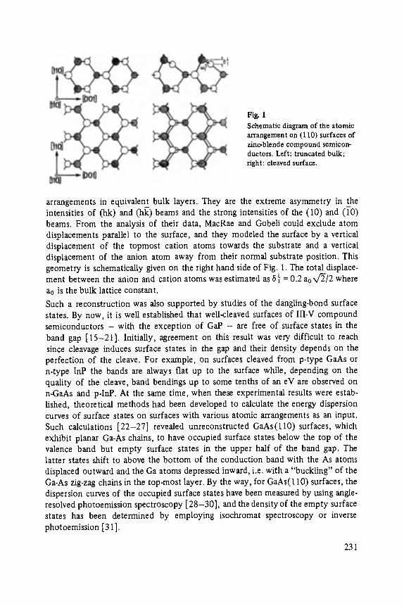
Fig. 1
Schematic diagram of the atomic arrangement on (110) surfaces of zinc-blende compound semicon- ductors. Left: truncated bulk; right: cleaved surface.
arrangements in equivalent bulk layers. They are the extreme asymmetry in the intensities of (hk) and (hk) beams and the strong intensities of the (10) and (1-0) beams. From the analysis of their data, MacRae and Gobeli could exclude atom displacements parallel to the surface, and they modeled the surface by a vertical displacement of the topmost cation atoms towards the substrate and a vertical displacement of the anion atom away from their normal substrate position. This geometry is schematically given on the right hand side of Fig. 1. The total displace- ment between the anion and cation atoms was estimated as ~lt = 0.2 aox/~/2 where ao is the bulk lattice constant.
Such a reconstruction was also supported by studies of the dangling-bond surface states. By now, it is well established that well-cleaved surfaces of III-V compound semiconductors - with the exception of GaP - are free of surface states in the band gap [15-21]. Initially, agreement on this result was very difficult to reach since cleavage induces surface states in the gap and their density depends on the perfection of the cleave. For example, on surfaces cleaved from p-type GaAs or n-type Imp the bands are always flat up to the surface while, depending on the quality of the cleave, band bendings up to some tenths of an eV are observed on n-GaAs and p-ImP. At the same time, when these experimental results were estab- lished, theoretical methods had been developed to calculate the energy dispersion curves of surface states on surfaces with various atomic arrangements as an input. Such calculations [22-27] revealed unreconstructed GaAs( l l0) surfaces, which exhibit planar Ga-As chains, to have occupied surface states below the top of the valence band but empty surface states in the upper half of the band gap. The latter states shift to above the bottom of the conduction band with the As atoms displaced outward and the Ga atoms depressed inward, i.e. with a "buckling" of the Ga-As zig-zag chains in the top-most layer. By the way, for GaAs(110) surfaces, the dispersion curves of the occupied surface states have been measured by using anne- resolved photoemission spectroscopy [28-30], and the density of the empty surface states has been determined by employing isochromat spectroscopy or inverse photoemission [31 ].
231
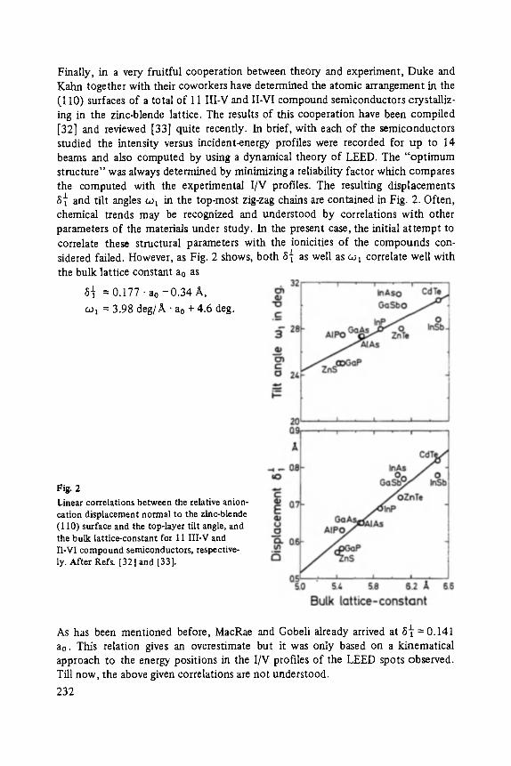
Finally, in a very fruitful cooperation between theory and experiment, Duke and Kahn together with their coworkers have determined the atomic arrangement in the (110) surfaces of a total of 11 III-V and II-VI compound semiconductors crystalliz- ing in the zinc-blende lattice. The results of this cooperation have been compiled [32] and reviewed [33] quite recently. In brief, with each of the semiconductors studied the intensity versus incident-energy profiles were recorded for up to 14 beams and also computed by using a dynamical theory of LEED. The "optimum structure" was always determined by minimizing a reliability factor which compares the computed with the experimental I/V profiles. The resulting displacements 8~ and tilt angles col in the top-most zig-zag chains are contained in Fig. 2. Often, chemical trends may be recognized and understood by correlations with other parameters of the materials under study. In the present case, the initial attempt to correlate these structural parameters with the ionicities of the compounds con- sidered failed. However, as Fig. 2 shows, both 8it as well as co~ correlate well with the bulk lattice constant a0 as
8~ = 0.177 �9 ao -0 .34 A,
col --- 3.98 deg/A �9 ao + 4.6 deg.
F~ 2 Linear correlations between the relative anion- cation displacement normal to the zinc-blende (110) surface and the top-layer tilt angle, and the bulk lattice-constant for 11 III-V and II-VI compound semiconductors, respective- ly. After Refs. [321 and [331.
As has been mentioned before, MacRae and Gobeli already arrived at 8~ = 0.141 ao. This relation gives an overestimate but it was only based on a kinematical approach to the energy positions in the I/V profiles of the LEED spots observed. Till now, the above given correlations are not understood.
232
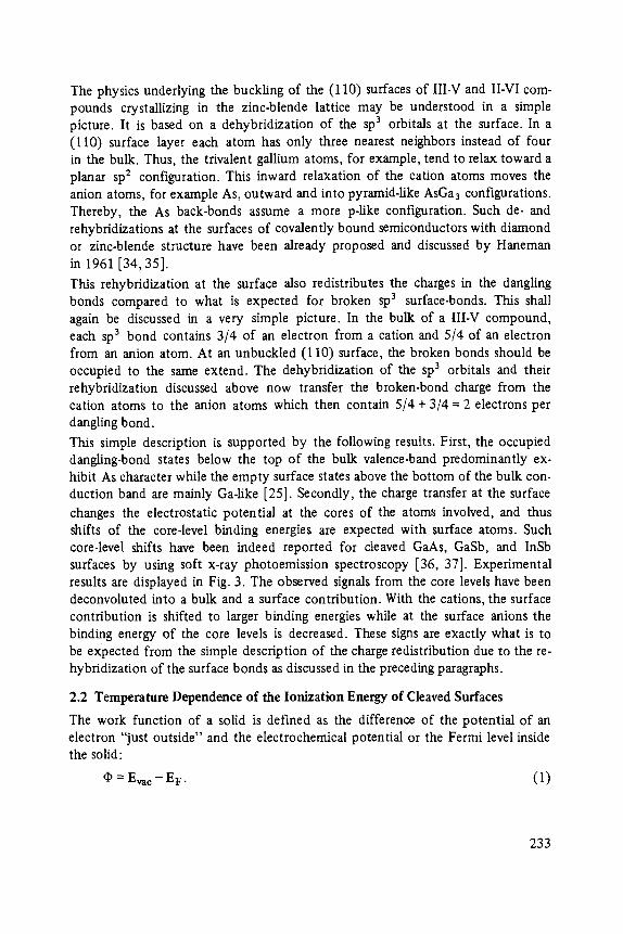
The physics underlying the buckling of the (110) surfaces of III-V and II-VI com- pounds crystallizing in the zinc-blende lattice may be understood in a simple picture. It is based on a dehybridization of the sp 3 orbitals at the surface. In a (110) surface layer each atom has only three nearest neighbors instead of four in the bulk. Thus, the trivalent gallium atoms, for example, tend to relax toward a planar sp 2 configuration. This inward relaxation of the cation atoms moves the anion atoms, for example As, outward and into pyramid-like AsGa3 configurations. Thereby, the As back-bonds assume a more p-like configuration. Such de- and rehybridizations at the surfaces of covalently bound semiconductors with diamond or zinc-blende structure have been already proposed and discussed by Haneman in 1961 [34, 35].
This rehybridization at the surface also redistributes the charges in the dangling bonds compared to what is expected for broken sp 3 surface-bonds. This shall again be discussed in a very simple picture. In the bulk of a tII-V compound, each sp 3 bond contains 3/4 of an electron from a cation and 5/4 of an electron from an anion atom. At an unbuckled (110) surface, the broken bonds should be occupied to the same extend. The dehybridization of the sp 3 orbitals and their rehybridization discussed above now transfer the broken-bond charge from the cation atoms to the anion atoms which then contain 5/4 + 3/4 = 2 electrons per dangling bond.
This simple description is supported by the following results, First, the occupied dangling-bond states below the top of the bulk valence-band predominantly ex- hibit As character while the empty surface states above the bottom of the bulk con- duction band are mainly Ga-like [25]. Secondly, the charge transfer at the surface
changes the electrostatic potential at the cores of the atoms involved, and thus shifts of the core-level binding energies are expected with surface atoms. Such core-level shifts have been indeed reported for cteaved GaAs, GaSb, and InSb surfaces by using soft x-ray photoemission spectroscopy [36, 37]. Experimental results are displayed in Fig. 3. The observed signals from the core levels have been deconvoluted into a bulk and a surface contribution. With the cations, the surface contribution is shifted to larger binding energies while at the surface anions the binding energy of the core levels is decreased. These signs are exactly what is to be expected from the simple description of the charge redistribution due to the re- hybridization of the surface bonds as discussed in the preceding paragraphs.
2.2 Temperature Dependence of the Ionization Energy of Cleaved Surfaces
The work function of a solid is defined as the difference of the potential of an electron "just outside" and the electrochemical potential or the Fermi level inside the solid:
q5 = Eva c - EF. (1)
233
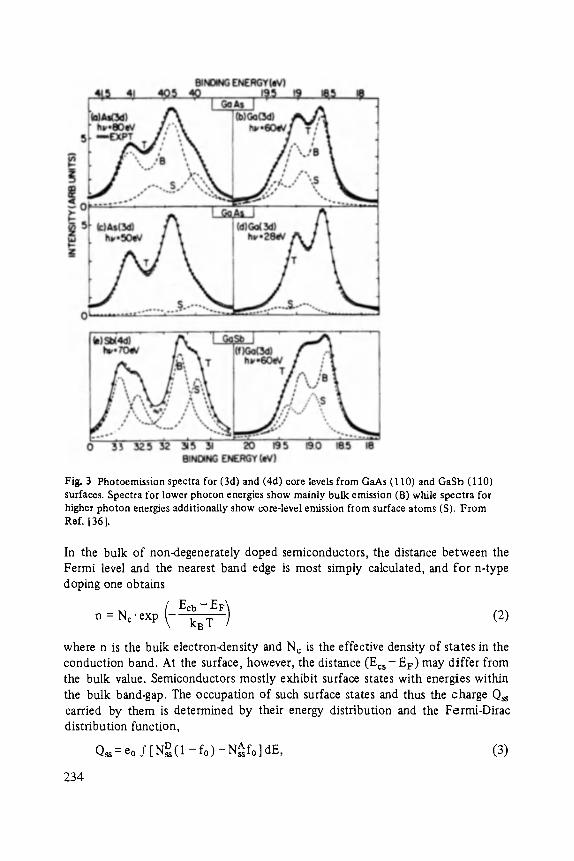
Fig. 3 Photoemission spectra for (3d) and (4d) core levels from GaAs (110) and GaSb (110) surfaces. Spectra for lower photon energies show mainly bulk emission (B) while spectra for higher photon energies additionally show core-level emission from surface atoms (S). From Ref. [361.
In the bulk of non-degenerately doped semiconductors, the distance between the Fermi level and the nearest band edge is most simply calculated, and for n-type doping one obtains
Ecb - EFI n = N c ' e x p Q kB-T 7 (2)
where n is the bulk electron-density and N~ is the effective density of states in the conduction band. At the surface, however, the distance (Ees- EF) may differ from the bulk value. Semiconductors mostly exhibit surface states with energies within the bulk band-gap. The occupation of such surface states and thus the charge Qss carried by them is determined by their energy distribution and the Fermi-Dirac distribution function,
Qss = e0 ; [ND(1 - f0) - NAfo] dE, (3)
234
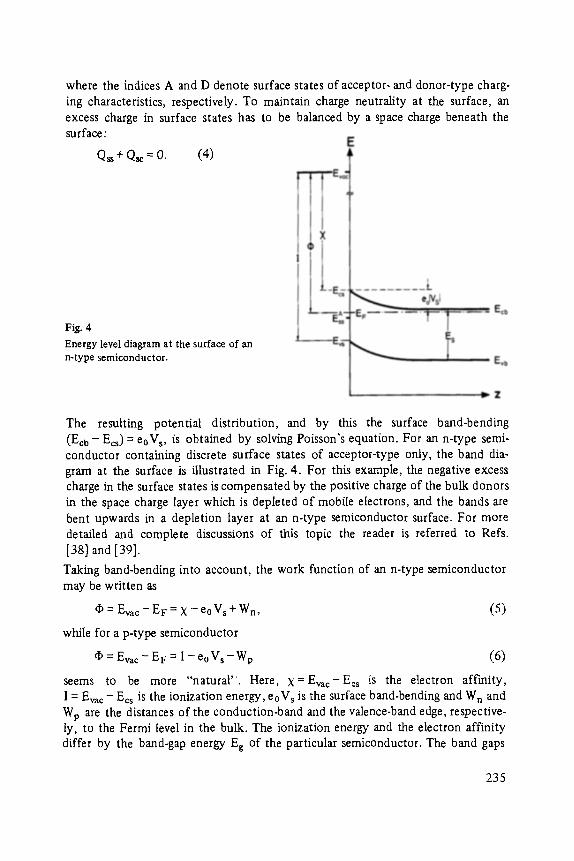
where the indices A and D denote surface states of acceptor- and donor-type charg- ing characteristics, respectively. To maintain charge neutrality at the surface, an excess charge in surface states has to be balanced by a space charge beneath the surface:
Qss + Qsc = 0. (4)
Fig. 4 Energy level diagram at the surface of an n-type semiconductor.
The resulting potential distribution, and by this the surface band-bending (Ecb - Ecs) = e0Vs, is obtained by solving Poisson's equation. For an n-type semi- conductor containing discrete surface states of acceptor-type only, the band dia- gram at the surface is illustrated in Fig. 4. For this example, the negative excess charge in the surface states is compensated by the positive charge of the bulk donors in the space charge layer which is depleted o f mobile electrons, and the bands are bent upwards in a depletion layer at an n-type semiconductor surface. For more detailed and complete discussions of this topic the reader is referred to Refs. [38] and [39].
Taking band-bending into account, the work function of an n-type semiconductor may be written as
�9 = E~ac - Er = • - eoVs + Wn, (5)
while for a p-type semiconductor
q~ = E~ac - E~- = I - eo Vs - Wp (6)
seems to be more "natural". Here, X = E~ac-Ees is the electron affinity, I = E~ac - Ecs is the ionization energy, eoV s is the surface band-bending and W n and Wp are the distances of the conduction-band and the valence-band edge, respective- ly, to the Fermi level in the bulk. The ionization energy and the electron affinity differ by the band-gap energy Eg of the particular semiconductor. The band gaps
235
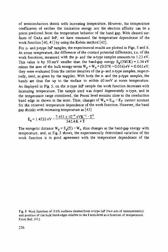
of semiconductors shrink with increasing temperature. However, the temperature coefficients of neither the ionization energy nor the electron affinity can be a priori predicted from the temperature behavior of the band gap. With cleaved sur- faces of GaAs and InP, we have measured the temperature dependence of the work function [40, 41] by using the Kelvin method [42].
For n- and p-type InP samples, the experimental results are plotted in Figs. 5 and 6. At room temperature, the difference of the contact potential differences, i.e. of the work functions, measured with the p- and the n-type samples amounts to 1.22 eV. This value is by 50 meV smaller than the band-gap energy Eg(300K)= 1.34eV minus the sum of the bulk energy-terms Wp + Wn = (0.078 - 0.016) eV = 0.062 eV; they were evaluated from the carrier densities of the p- and n-type samples, respect- ively, used, as given by the supplier. With both the n- and the p-type samples, the bands are thus fiat up to the surface to within 60 meV at room temperature.
As displayed in Fig. 5, on the n-type InP sample the work function decreases with increasing temperature. The sample used was doped degenerately n-type, and in the temperature range considered, the Fermi level remains close to the conduction band edge as shown in the inset. Thus, changes of W n = Ecb - E F cannot account for the observed temperature dependence of the work function. However, the band gap shrinks with increasing temperature as [43]
7.451 • 10 -4 eVK -1 �9 T 2 Eg = 1.4233 eV
542.4K + T
The energetic distance Wp = Eg(T) - W n thus changes as the band-gap energy with temperature, and, as Fig. 5 shows, the experimentally determined variation of the work function is in good agreement with the temperature dependence of the
Fig. 5 Work function of (110) surfaces cleaved from n-type InP (two sets of measurements) and position of the bulk band-edges relative to the Fermi-level as a function of temperature. From Ref. [41].
236
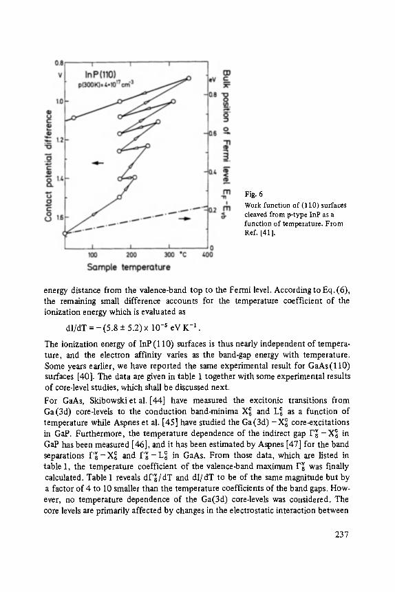
Fig. 6 Work function of (110) surfaces cleaved from p-type InP as a function of temperature. From Ref. [411.
energy distance from the valence-band top to the Fermi level. According to Eq. (6), the remaining small difference accounts for the temperature coefficient of the ionization energy which is evaluated as
dl/dT = - (5.8 + 5.2) x i0 -s eV K -1 .
The ionization energy of InP (110) surfaces is thus nearly independent of tempera- ture, and the electron affinity varies as the band-gap energy with temperature. Some years earlier, we have reported the same experimental result for GaAs (110) surfaces [40]. The data are given in table 1 together with some experimental results of core-level studies, which shall be discussed next.
For GaAs, Skibowski et al. [44] have measured the excitonic transitions from Ga(3d) core-levels to the conduction band-minima X~ and L~ as a function of temperature while Aspnes et al. [45] have studied the Ga (3d) -X~ core-excitations
v r in GaP. Furthermore, the temperature dependence of the indirect gap [ ' 8 - X6 in GaP has been measured [46], and it has been estimated by Aspnes [47] for the band separations P ~ - X~ and [ ' ~ - L~ in GaAs. From those data, which are listed in table 1, the temperature coefficient of the valence-band maximum P~ was finally calculated. Table 1 reveals dP~/dT and dI/dT to be of the same magnitude but by a factor of 4 to 10 smaller than the temperature coefficients of the band gaps. How- ever, no temperature dependence of the Ga(3d) core-levels was considered. The core levels are primarily affected by changes in the electrostatic interaction between
237

Table 1 Temperature coefficients of core-level excitons, band separations, and ionization energy of (110) surfaces
Semiconductor Transition dEt/dT dI'~/dT d l l lo /dT in meV K -1 in meV K-I in meV K -1
lnP
~qaAs
3aP
rX Ga(3d)- X~
Ga(3d)- L~
rE- Ga(3d)- X~
= 0.52 a) - 0.25 • 0.03 b)
- 0 . 3 8 c)
- 0 . 3 1 • 0 . 0 3 b )
- 0.47 d)
- 0.24 -+ 0.05 e)
- 0.320
+ 0.13
+ 0.16
+ 0.08
- 0.06 • 0.05 g) + 0.02 • 0.06 h)
a) Ref. [43], T = 450 K b) Ref. [44], T = 4 ... 300 K c) Ref. [47], T = 300 K d) ReL [45], T = 300 K
f) Ref. [46],T = 200 K g) Ref. [41],T = 300 ... 630K h) Ref. [40], T = 100 ... 300 K
screened bond and core charges and by the redistr ibut ion o f the bond charges wi th
changing temperature . For GaP, bo th effects have been est imated to con t r ibu te less
than 0.01 m e V K -1 [45].
The temperature coeff ic ient o f the valence-band max imum may also be es t imated
f rom theory. One has to consider contr ibut ions arising f rom the Debye-Waller
effect [48], the e lectron self-energy [49], the lattice expansion or the hydros ta t ic
shift, and the reference potent ia l o f the sp 3 bands, i.e. the Vo0o form fac tor . Ex-
cept for the hydrostat ic term, the o ther contr ibut ions have been calculated for the
valence-band max imum F~ of GaAs [50, 51]. They are listed in table 2. The hydro-
static te rm is usually calculated f rom the thermal expansion coeff ic ient , the iso-
Table 2 Contributions and total value of the tempera- ture coefficient of the valence-band top r~ and tem- perature coefficient of the ionization energy of (110) surface of GaAs.
Term dE/dT in meV K -l
Debye-Waller Electron Self-Energy Hydrostatic Vooo Total Ionization energy
+ 0.245 a) + 0.004 b) - 0.22 c) + 0.021 d) + 0.086 + 0.02 • 0.06 e)
a) ReL [50] b) Ref. [51] c) See text d) Ref. [44] e) Ref. [40]
238
thermal compressibility ~, and the pressure coefficient of the particular transition considered through the relation
dE,/ dE,/ aT yd = -~-" dP/T" (7)
Since the pressure coefficient of the F~ - X~ transition has been given by Aspnes [47] and since Skibowski et al. [44] have calculated the hydrostatic term to the temperature coefficient of the X~ conduction band minimum, the hydrostatic contribution to the temperature variation of the valence-band maximum F~ itself may be evaluated. As table 2 shows, the resulting total temperature coefficient of the valence-band top agrees quite well with the experimental temperature dependence of the ionization energy. This conclusion shall not be overestimated since many approximations enter into the theoretical evaluations and the limits of experimental accuracy are quite large. However, at least for GaAs and InP, both theory and experiment establish the top of the valence-band to be much less sensitive to changes in temperature than the bottom of the conduction band. There- fore, Eq. (6) containing the ionization energy seems to be the more appropriate expression for the work function for both p- as well as n-type semiconductors rather than Eq. (5).
2.3 Chemical Trends of the Ionization Energy of (110) Surfaces
For semiconductors it is quite difficult to calculate the ionization energy of a particular surface since the valence electrons are concentrated in the bond and the surfaces are reconstructed. However, chemical trends may be obtained from LCAO (Linear Combination of Atomic Orbitals)-type calculations of the electronic struc- ture [52, 53]. In the LCAO description, the electronic band structure is derived from atomic term values and interatomic matrix elements. For compound semi- conductors crystallizing in the zinc-blende lattice the energy of the valence-band top I~ is given by [54]
C - - a
Ep (8) Ev 2
E~ and E~ are the atomic term values of the p-orbitals of the cation and the anion in a CA compound, respectively. V3 = I/2(E~ + E~) is the polar energy, and V2 -- 2.16 h2/mod 2 is the interatomic matrix element or the covalent energy. The atomic term values as calculated by Herman and SkiIlman [55] may be found in Ref. [52].
The atomic term values are measured from the vacuum level, and therefore Eq. (8) also gives the energy position of the valence-band maximum below the vacuum level, i.e. the ionization energy. Experimentally, the ionization energy of a semi- conductor is given by the threshold energy of the total yield-versus-photon energy curves in photoemission spectroscopy studies. In Fig. 7, the experimentally deter-
239
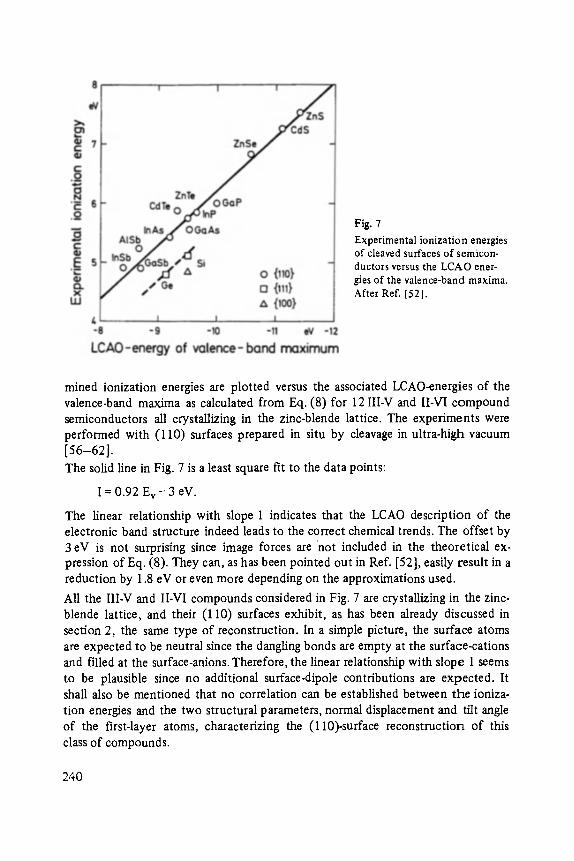
Fig. 7 Experimental ionization energies of cleaved surfaces of semicon- ductors versus the LCAO ener- gies of the valence-band maxima. After Ref. 1521.
mined ionization energies are plotted versus the associated LCAO-energies of the valence-band maxima as calculated from Eq. (8) for 12 III-V and II-VI compound semiconductors all crystallizing in the zinc-blende lattice. The experiments were performed with (1 I0) surfaces prepared in situ by cleavage in ultra-high vacuum [56-62].
The solid line in Fig. 7 is a least square fit to the data points:
I = 0.92 Ev - 3 eV.
The linear relationship with slope 1 indicates that the LCAO description of the electronic band structure indeed leads to the correct chemical trends. The offset by 3 eV is not surprising since image forces are not included in the theoretical ex- pression of Eq. (8). They can, as has been pointed out in Ref. [52], easily result in a reduction by 1.8 eV or even more depending on the approximations used.
All the III-V and II-VI compounds considered in Fig. 7 are crystallizing in the zinc- blende lattice, and their (110) surfaces exhibit, as has been already discussed in section 2, the same type of reconstruction. In a simple picture, the surface atoms are expected to be neutral since the dangling bonds are empty at the surface-cations and filled at the surface-anions. Therefore, the linear relationship with slope 1 seems to be plausible since no additional surface-dipole contributions are expected. It shall also be mentioned that no correlation can be established between the ioniza- tion energies and the two structural parameters, normal displacement and tilt angle of the first-layer atoms, characterizing the (110)-surface reconstruction of this class of compounds.
240
The data points of cleaved Ge and Si (111) surfaces [56, 57] are shown in Fig. 7 for reasons of comparison. They do not follow the fit to the results for the (110) surfaces of the compounds, however, they may be connected by a straight line shifted by 0.6eV to lower ionization energies. The cleaved Ge and Si surfaces both exhibit a 2 x 1 reconstruction [56] which was considered to be adequately described by a buckling model [34, 35, 63, 64] until the 7r-bonded chain model was proposed [65]. In the buckling model, adjacent rows of atoms in the terminat- ing (111) plane are raised and depressed with respect to a common plane which as a whole is relaxed inward while the 7r-bonded chain model contains two terminat- ing (110) layers which are connected to the underlying (111)-oriented bulk by 5- and 7-membered rings. Recent experiments [66-68] seem to support the 7r- bonded chain model but most probably the chains need to be buckled [69].
2.4 Compositional Trends of the Ionization Energies of Polar GaAs Surfaces
The work function of metals is known to vary by some tenths of an eV for differ- ently oriented surfaces. Already in 1941, Smoluchowski [70] has given some simple arguments for a physical understanding of the trends observed. First of all, the potential well at a surface is finite, and thus the electrons "tail" into vacuum leaving part of the positively charged atom-cores uncompensated. The dipole layer formed increases the work function. Secondly, the electrons may also redistribute laterally. In a simple picture, every atom in a metal "fills" a Wiguer-Seitz cell which is a rhombic dodecahedron for face-centered cubic lattices. The surfaces axe thus rough, and electrons may flow from "hills" into "valleys" at the surface leaving part of the positive charge in the Wigner-Seitz ceils uncompensated. This "smooth- hag" effect lowers the work function, and the decrease should be larger on rough surfaces. Among the low-indexed faces of a fcc metal, the (111) planes are most densely packed, and they are followed by the (100) and the (110) planes. Indeed, the work functions were found to decrease in that order (see for example Ref. [71] and [72]).
Such simple models cannot be applied to semiconductors since their surfaces are re- constructed, and with compound semiconductors we additionally have to consider variations in surface composition. Even for a bulk-truncated binary compound ex- hibiting zinc-blende structure, the (110) planes contain anions and cations in equal density while (100) as well as (11 l) oriented surfaces are terminated by either anion or cation atoms. However, with such surfaces generally more than one reconstruc- tion has been observed each of which has a different surface composition. As an example, some of the results reported for GaAs(100) surfaces are listed in Fig. 8. Surfaces of this orientation have been studied in great detail since they are of technological importance for epitaxial growth in device applications. As Fig. 8 shows, there is still a large scatter in the data of the chemical compositions for most of the reconstructions. Part of the differences are caused by difficulties in the preparation of such surfaces by molecular beam epitaxy.
241

Fig. 8 Correlation between atomic arrangement and chemical composition on GaAs(001) surfaces (A from Ref. 174], o from Ref. 175 ], n from Ref. [761, V from Ref. [77 ], A x from Ref. I73]).
Table 3 Compositional dependence of electronic surface parameters of GaAs(100) surfaces.
1 q~ E F - Evs I Reconstruction 0As in eV in eV in eV
4x6
c(2 x 8)
c(4 x 4)
~. 0.2 a)
1 a )
> 1 g)
4.95 b)
5.15 b)
4.85 b)
0.73 c) 0.45 d) 0.4 e)
0.4 e) 0.76 d)
5.68 5.4
5.55 5.4 f)
5.25 5.61
a) Ref. [75] e) Ref. [80] b) Ref. [76] f) Ref. [81] (see text) c) Ref. [78] g) Ref.[76, 82] d) Ref. [79]
Only very few results have been published on the work function, the band bending or the ionization energy in clean surfaces of III-V compound semiconductors other than cleaved surfaces. For GaAs (100) surfaces, exhibiting different reconstructions
and thus different surface compositions, the data published are compiled in Tab. 3. Evidently, from the results published up to now, no conclusions can be drawn with regard to a possible trend in the ionization energy of GaAs(100) surfaces as a func- tion of As coverage. Further studies are needed to clarify on this subject.
242
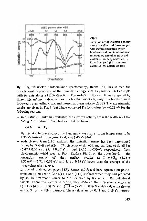
Fig. 9 Variation of the ionization energy around a cylindrical GaAs sample with surfaces prepared by ion bomba, dment, ion bombardment followed by annealing (iba) and molecular beam epitaxy (MBE). Data from ReL [81] have been corrected; for details see text.
By using ultraviolet photoemission spectroscopy, Ranke [81] has studied the orientational dependence of the ionization energy with a cylindrical GaAs sample with its axis along a (1]-0) direction. The surface of the sample was prepared by three different methods which are ion bombardment (ib) only, ion bombardment followed by annealing (iba), and molecular beam epitaxy (MBE). The experimental results are given in Fig. 9, but I have corrected Ranke's values by - 0.23 eV for the following reasons:
- In his study, Ranke has evaluated the electron affinity from the width W of the energy distribution of the photoernitted electrons:
• = h ~ o - W - E g .
By mistake, he has assumed the band-gap energy Eg at room temperature to be 1.35 eV instead of the correct value of 1.43 eV [46].
- With cleaved GaAs( l l0) surfaces, the ionization energy has been determined earlier by Gobeli and Allen [57], Sebenne et al. [60], and van Laar et al. [61] as (5.47 + 0.05)eV, (5.4 -+ 0.05)eV, and (5.56 -+ 0.05)eV, respectively, from photoemission-yield spectra. From Ranke's Fig. 2, on the other hand, the ionization energy of that surface results as I -- • + Eg = (4.36 + 1.35)eV=(5.71-+ 0.03)eV and is by 0.25 eV larger than the average of the three values given above.
- In one of their earlier paper [83], Ranke and Jacobi have reported on photo- emission studies with GaAs(111) and (111) surfaces which they had prepared by an iba treatment similar to the one used by Ranke with the cylindrical sample. From the spectra recorded, they deduced the ionization energies as I (111) -- (4.83 -+ 0.03) eV and I (111) = (5.27 -+ 0.03) eV which values are shown in Fig. 9 by the filled triangles. These values are by 0.41 and 0.19 eV, respec-
243
tively, larger than the ones now communicated by Ranke but they are close to the corrected data.
We shall now discuss Ranke's results with respect to the surface preparation. After the ion bombardment, the surfaces are completely disordered and depleted of arsenic [84, 85]. Thus, it is not surprising that the ionization energy is almost independent of the surface orientation and quite low, as shall be explained later. A following annealing treatment generally increases the ionization energy. On ion- bombarded and annealed GaAs as well as InP(110) surfaces large Ga and In islands, respectively, are visible even in an optical microscope [84, 86], and the LEED patterns are identical to those observed with cleaved surfaces [86-88] since the sur- face area uncovered by the cation bubbles is well ordered again. On the MBE- grown film, the ionization energy is further increased with the exception of the (11 I) oriented face. GaAs(111) surfaces can be only prepared exhibiting a 2 x 2 re- construction, and they are terminated by a complete Ga layer, as is also expected for a truncated bulk. For the other surfaces, the experimental conditions were chosen such as to grow the As-terminated (001) - c(2 x 8), (001-) - c(2 • 8), and (111") - 2 x 2 surfaces. Therefore, it is not surprising that the ionization energies only vary by approximately 0.15 eV on these surfaces but are larger by approxi- mately 0.4 eV on the Ga-terminated (I 11) - 2 x 2 surface. From Pauling's concept of the ionicity of covalent bonds [89], these findings seem to be plausible. The elec- tronegativity of As atoms is by 0.4 larger than of Ga atoms, and thus, Ga-As bonds should be by 4 % ionic with the As and Ga atoms being negatively and positively charged, respectively. The geometrical orientation of such "chemical" Ga § - As -q surface dipoles should then result in a larger ionization energy on As-terminated compared with Ga-terminated surfaces. This is, indeed, the experimental result. Therefore, a trend of the ionization energy might also be expected with (001) surfaces as a function of As-coverage.
3 Ge: III-V Hete ro junc t ions
In semiconductor devices, metal-semiconductor and oxide-semiconductor interfaces play an essential role since long. With the applications of III-V compound semi- conductors, semiconductor heterojunctions also became part of many modern devices [11]. Completely new device concepts [10, 90] based not only on doping but also on compositional superlattices could be and will become realized due to the improvements in the growth of epitaxial layers achieved by molecular beam epitaxy (MBE) and metal-organic vapor-phase epitaxy (MOVPE). A number of heterojunc- tions have been studied in some detail, however, the Ge:GaAs heterostructure, which may be most simply prepared by evaporation of Ge on clean GaAs surfaces, has attracted much interest recently [91-111].
Germanium and gallium arsenide crystallize in the diamond and the zinc-blende lattice, respectively, and their lattice constants differ by only 0.08 % since the three
244
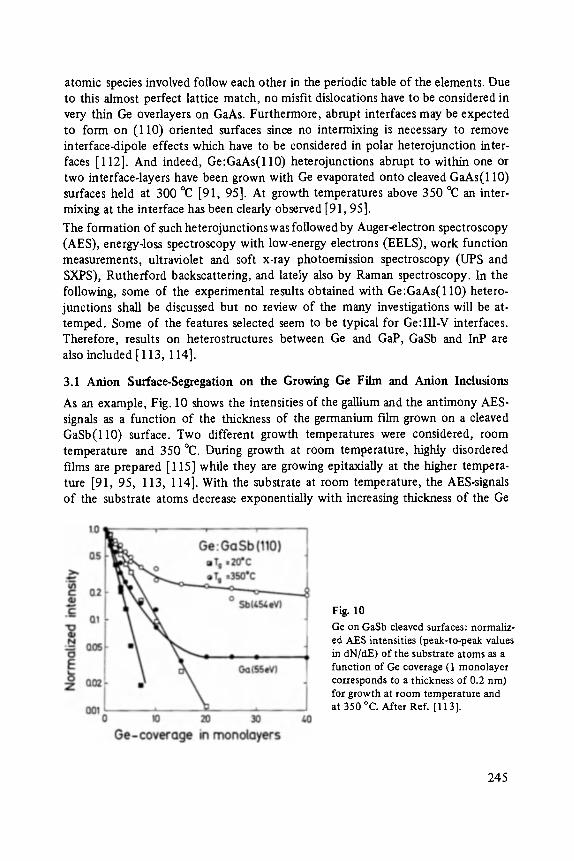
atomic species involved follow each other in the periodic table of the elements. Due to this almost perfect lattice match, no misfit dislocations have to be considered in very thin Ge overlayers on GaAs. Furthermore, abrupt interfaces may be expected to form on (110) oriented surfaces since no intermixing is necessary to remove interface-dipole effects which have to be considered in polar heterojunction inter- faces [112]. And indeed, Ge:GaAs(1 I0) heterojunctions abrupt to within one or two interface-layers have been grown with Ge evaporated onto cleaved GaAs(110) surfaces held at 300 ~ [91, 95]. At growth temperatures above 350 ~ an inter- mixing at the interface has been clearly observed [91, 95].
The formation of such heterojunctions was followed by Auger-electron spectroscopy (AES), energy-loss spectroscopy with low-energy electrons (EELS), work function measurements, ultraviolet and soft x-ray photoemission spectroscopy (UPS and SXPS), Rutherford backscattering, and lately also by Raman spectroscopy. In the following, some of the experimental results obtained with Ge:GaAs(110) hetero- junctions shall be discussed but no review of the many investigations will be at- temped. Some of the features selected seem to be typical for Ge:III-V interfaces. Therefore, results on heterostructures between Ge and GaP, GaSb and InP are also included [113, 114].
3.1 Anion Surface-Segregation on the Growing Ge Film and Anion Inclusions
As an example, Fig. 10 shows the intensities of the gallium and the antimony AES- signals as a function of the thickness of the germanium film grown on a cleaved GaSb(l l0) surface. Two different growth temperatures were considered, room temperature and 350 ~ During growth at room temperature, highly disordered films are prepared [115] while they are growing epitaxially at the higher tempera- ture [91, 95, 113, 114]. With the substrate at room temperature, the AES-signals of the substrate atoms decrease exponentially with increasing thickness of the Ge
Fig. 10 Ge on GaSb cleaved surfaces: normaliz- ed AES intensities (peak-to-peak values in dN/dE) of the substrate atoms as a function of Ge coverage (1 monolayer corresponds to a thickness of 0.2 rim) for growth at room temperature and at 350 ~ After Ref. [113].
245

film, indicating the growth of a continuous film which conclusion has been con- firmed for Ge:GaAs by reflection high-energy electron diffraction (RHEED) [102]. During growth at 350 ~ the AES signals from both types of substrate atoms initially decreases with the same slope observed during growth at room temperature, and for larger coverages they level off with the relative intensity of the Sb signal exceeding that of the Ga signal. These results are caused by a surface segregation of both Ga and Sb on top of the growing Ge film. The same behavior has also been observed with the other Ge:III-V heterojunctions studied [95, 113, 1141 .
Such surface segregation of substrate atoms at the surfaces of Ge films grown at or above 300 ~ may be also observed during a removal of the films by using argon ions. Fig. 11 shows a sputter profile of such a Ge:GaAs heterojunction [ 116]. The data clearly reveal the surface segregation of both arsenic and gallium atoms. The sputter rate may be determined from that part of the profile which exhibits the exponential increase of the substrate signals as a function of the sputter time since the interface is abrupt to within one or two monolayers [91, 95] and the escape depths are known [ 117]. Thus, the time scale may be converted into film thickness removed by sputtering as given by the upper scale of Fig. 11. For an abrupt junc- tion the extrapolation of the exponentially increasing portion of the profile then gives the position of the interface which value quite well agrees with the nominal
Fig. 11 AES sputter-profile of a Ge:GaAs (110) heterojunction grown at 300 ~ The nominal thickness of the Ge film amounted to (6 -+ 0.4) nm as determined from the Ge evaporation-rate. After Ref. [ 116 ].
246
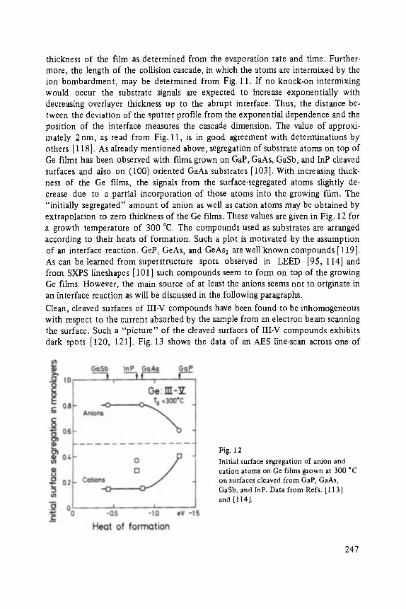
thickness of the film as determined from the evaporation rate and time. Further- more, the length of the collision cascade, in which the atoms are intermixed by the ion bombardment, may be determined from Fig. 11. If no knock-on intermixing would occur the substrate signals are expected to increase exponentially with decreasing overlayer thickness up to the abrupt interface. Thus, the distance be- tween the deviation of the sputter profile from the exponential dependence and the position of the interface measures the cascade dimension. The value of approxi- mately 2nm, as read from Fig. 11, is in good agreement with determinations by others [ 118]. As already mentioned above, segregation of substrate atoms on top of Ge films has been observed with films grown on GaP, GaAs, GaSb, and InP cleaved surfaces and also on (100) oriented GaAs substrates [103]. With increasing thick- ness of the Ge films, the signals from the surface-segregated atoms slightly de- crease due to a partial incorporation of those atoms into the growing film. The "initially segregated" amount of anion as well as cation atoms may be obtained by extrapolation to zero thickness of the Ge films. These values are given in Fig. 12 for a growth temperature of 300 ~ The compounds used as substrates are arranged according to their heats of formation. Such a plot is motivated by the assumption of an interface reaction. GeP, GeAs, and GeAs2 are well known compounds [119]. As can be learned from superstructure spots observed in LEED [95, 114] and from SXPS lineshapes [101] such compounds seem to form on top of the growing Ge films. However, the main source of at least the anions seems not to originate in an interface reaction as will be discussed in the following paragraphs.
Clean, cleaved surfaces of III-V compounds have been found to be inhomogeneous with respect to the current absorbed by the sample from an electron beam scanning the surface. Such a "picture" of the cleaved surfaces of III-V compounds exhibits dark spots [120, 121]. Fig. 13 shows the data of an AES line-scan across one of
Fig. 12 Initial surface segregation of anion and cation atoms on Ge films grown at 300 ~ on surfaces cleaved from GaP, GaAs, GaSb, and InP. Data from Refs. [1131 and [1141.
247
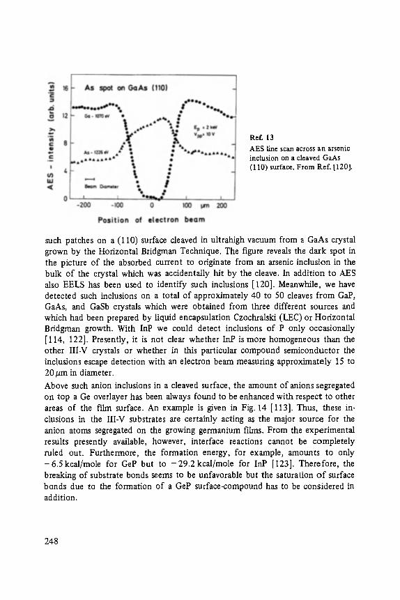
Ref. 13
AES line scan across an arsenic inclusion on a cleaved GaAs (110) surface. From Ref. [120].
such patches on a (110) surface cleaved in ultralfigh vacuum from a GaAs crystal grown by the Horizontal Bridgman Technique. The figure reveals the dark spot in the picture of the absorbed current to originate from an arsenic inclusion in the bulk of the crystal which was accidentally hit by the cleave. In addition to AES also EELS has been used to identify such inclusions [120]. Meanwhile, we have detected such inclusions on a total of approximately 40 to 50 cleaves from GaP, GaAs, and GaSb crystals which were obtained from three different sources and which had been prepared by liquid encapsulation Czochralski (LEC) or Horizontal Bridgrnan growth. With InP we could detect inclusions of P only occasionally [114, 122]. Presently, it is not clear whether InP is more homogeneous tb.an the other III-V crystals or whether in this particular compound semiconductor the inclusions escape detection with an electron beam measuring approximately 15 to 20/~m in diameter.
Above such anion inclusions in a cleaved surface, the amount of anions segregated on top a Ge overlayer has been always found to be enhanced with respect to other areas of the film surface. An example is given in Fig. 14 [113]. Thus, these in- clusions in the III-V substrates are certainly acting as the major source for the anion atoms segregated on the growing germanium films. From the experimental resuIts presently available, however, interface reactions cannot be completely ruled out. Furthermore, the formation energy, for example, amounts to only -6.Skcal /mole for GeP but to -29 .2 kcal/mole for InP [123]. Therefore, the breaking of substrate bonds seems to be unfavorable but the saturation o f surface bonds due to tb.e formation of a GeP surface-compound has to be considered in addition.
248
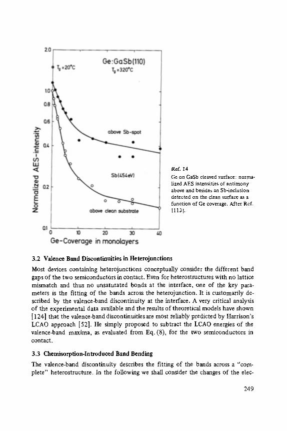
ReL 14 Ge on GaSb cleaved surface: norma- lized AES intensities of antimony above and besides an Sb-inclusion detected on the clean surface as a function of Ge coverage. After Ref. [113].
3.2 Valence Band Discontinuities in Heterojunctions
Most devices containing heterojunctions conceptually consider the different band gaps of the two semiconductors in contact. Even for heterostructures with no lattice mismatch and thus no unsaturated bonds at the interface, one of the key para- meters is the fitting of the bands across the heterojunction. It is customarily de- scribed by the valence-band discontinuity at the interface. A very critical analysis of the experimental data available and the results of theoretical models have shown [ 124] that the valence-band discontinuities are most reliably predicted by Harrison's LCAO approach [52]. He simply proposed to subtract the LCAO energies of the valence-band maxima, as evaluated from Eq. (8), for the two semiconductors in contact.
3.3 Chemisorption-Introduced Band Bending
The valence-band discontinuity describes the fitting of the bands across a "com- plete" heterostructure. In the following we shall consider the changes of the elec-
249
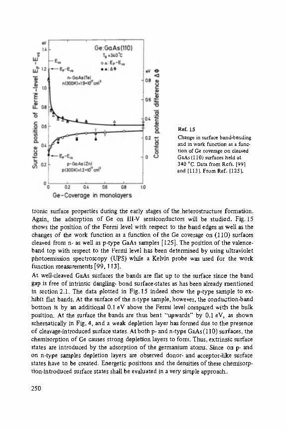
Ref, 15 Change in surface band-bending and in work function as a func- tion of Ge coverage on cleaved GaAs (I 10) surfaces held at 340 ~ Data from Refs. [99] and [1131. From Ref. [125].
tronic surface properties during the early stages of the.heterostructure formation. Again, the adsorption of Ge on III-V semiconductors will be studied. Fig. 15 shows the position of the Fermi level with respect to the band edges as well as the changes of the work function as a function of the Ge coverage on (110) surfaces cleaved from n- as well as p-type GaAs samples [ I25]. The position of the valence- band top with respect to the Fermi level has been determined by using ultraviolet photoemission spectroscopy (UPS) while a Kelvin probe was used for the work function measurements [99, 113].
At well-cleaved GaAs surfaces the bands are flat up to the surface since the band gap is free of intrinsic dangling- bond surface-states as has been already mentioned in section 2.1. The data plotted in Fig. 15 indeed show the p-type sample to ex- hibit flat bands. At the surface of the n-type sample, however, the conduction-band bottom is by an additional 0.1 eV above the Fermi level compared with the bulk position. At the surface the bands are thus bent "upwards" by 0.1 eV, as shown schematically in Fig. 4, and a weak depletion layer has formed due to the presence of cleavage-introduced surface states. At both p- and n-type GaAs (110) surfaces, the chemisorption of Ge causes strong depletion layers to form. Thus, extrinsic surface states are introduced by the adsorption of the germanium atoms. Since on p- and on n-type samples depletion layers are observed donor- and acceptor-like surface states have to be created. Energetic positions and the densities of these chemisorp- tion-introduced surface states shall be evaluated in a very simple approach.
250
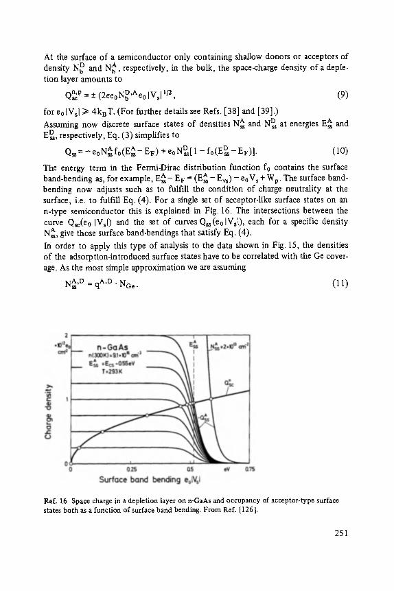
At the surface of a semiconductor only containing shallow donors or acceptors of density N~ and N~, respectively, in the bulk, the space,charge density of a deple- tion layer amounts to
Q~p = + (2eeoN~,Aeo iVs[ 1/2, (9)
for eo IVsl >--- 4kBT. (For further details see Refs. [38] and [39].)
Assuming now discrete surface states of densities N l and N~ at energies E l and E~, respectively, Eq. (3) simplifies to
_ A A _ + e o N ~ [ 1 - f o ( E ~ ( 1 0 ) Qss- - eoNss f0(Ess EF) - EF)].
The energy term in the Fermi-Dirac distribution function fo contains the surface band-bending as, for example, E l - Er = ( E l - Evs) - eoVs + Wp. The surface band- bending now adjusts such as to fulfill the condition of charge neutrality at the surface, i.e. to fulfill Eq. (4). For a single set of acceptor-like surface states on an n-type semiconductor this is explained in Fig. 16. The intersections between the curve Qsc(eo IVsl) and the set of curves Q~s(eolVsl), each for a specific density N l , give those surface band-bendings that satisfy Eq. (4).
In order to apply this type of analysis to the data shown in Fig. 15, the densities of the adsorption-introduced surface states have to be correlated with the Ge cover- age. As the most simple approximation we are assuming
NA,D = qA,D. NGe. (I I)
ReL 16 Space charge in a depletion layer on n-GaAs and occupancy of acceptor-type surface states both as a function of surface band bending. From Ref. [126].
251
With the above assumptions a least-square fit to the experimental data presented in Fig. 15 yields:
EAss - Evs = (0.72 -+ 0.05) eV, qn = 0.06 + 0.03,
EDss - Evs = (0.42 + 0.05) eV, qD = 0.04 -+ 0.02.
The curves drawn in Fig. 15 have been calculated by using these parameters, and they are explaining the quality of the fit.
In Fig. 15 the measured changes of the contact potential difference, i.e. the changes of the work function, are also plotted versus the surface coverage with germanium. Evidently, surface band-bending and work function vary to exactly the same ex- tend as a function of Ge coverage. Thus, according to Eq. (6), the adsorption of Ge does not change the ionization energy, i.e., no chemisorption-introduced surface dipoles are observed. Considering Pauling's concept of the partly ionic character of covalent bonds [ 89] these findings seem to be plausible. The ionicity of such bonds is determined by the difference in the electronegativities of the atoms involved. In the periodic table of the elements, Ga, Ge, and As follow each other in that se- quence, and the electronegativity of Ge is the average of those values for Ga and As. Thus, at least on the average, no chemisorption-related dipoles are expected for Ge adsorbed on GaAs.
After condensation of Ge on GaAs [ 113] as well as on InP cleaved surfaces [ 114] at room temperature, however, a change of the ionization energy and thus the forma- tion of chemisorption-introduced dipoles is observed. Since at room temperature the surface mobility is lower than at 300 ~ the Ge atoms seem to occupy different sites after condensation at both temperatures.
One problem remaining is to identify the physical origin of the adsorption- introduced surface states. Already Spicer and coworkers [127-129] had observed that the adsorption of A1, Ga, In, Cs, and oxygen in the submonolayer coverage. range causes the formation of depletion layers on both p- and n-type GaAs. They gave the final positions of the Fermi level with respect to the band edges at the surface to differ by 0.25 eV for both types of dopings. We could show that the set of surface states introduced by the adsorption of Ge on GaAs cleaved surfaces also fits the surface band-bending-versus-coverage curves for A1, Ga, In, and oxygen [98, 130]. These findings and the very low formation rates qA,O of the adsorption- introduced surface states support Spicer's early suggestions [127, 131, 132] that these extrinsic surface states are related to the formation of native defects in the substrate rather than to the specific atomic species adsorbed.
With respect to Ge:GaAs(110) this interpretation has been recently questioned by Brugger et al. [108], and they have proposed that dangling bonds of the Ge atoms adsorbed might be responsible for the band bending on the GaAs side of the hetero- junction even with thick Ge overlayers [ 101 ]. This interpretation of the data seems to be attractive but not convincing since at the surface of the Ge films the dangling
252

bonds are saturated by arsenic and since the same surface band-bending-versus- coverage curves are observed for metals, oxygen, and germanium.
In the framework of Spicer's defect model, vacancies [133-135], and antisite de- fects [136-138] have been proposed to account for the adsorption-introduced surface states. The presence of isolated vacancies seems to be very unlikely since in studies of radiation damage excess vacancies have been found to anneal out at 230 ~ [ 139] while the same band bending is observed after Ge depositions at room temperature and above 300 ~ The correlation of ASGa antisite defects with the surface states observed seems to be very attractive. This is for two reasons. In the bulk, ASGa antisite defects exhibit two levels [ 142] at the same energy as found for the adsorption-introduced surface states. Bulk ASGa antisite defects are double donors and can thus not pin the Fermi level at the surfaces of n- and p-type samples which, however, may be achieved by the introduction of additional acceptors [126]. This proposal is supported by finding that the chemisorption-introduced surface band-bending decays on p-type samples during annealing above 400 ~ but persists on n-type samples [113, 140]. An identical annealing behavior has been reported for ASGa antisite defects produced by neutron irradiation [141] or by plastic deformation [142].
The level matching and the identical annealing behavior strongly suggest that the surface band-bending after the adsorption of Ge on GaAs(110) surfaces might be related with ASGa antisite defects. However, such correlations are "finger prints" rather than proofs, and additional experimental studies are needed and additional experimental tools have to be applied to clarify this subject.
4 Oxida t ion o f GaAs (110) Surfaces
During the past 20 years the uptake of oxygen by clean III-V surfaces has been studied by using quite a number of different experimental tools. However, in only very few of those investigations different techniques have been simultaneously applied, and thus seemingly disagreeing results and, above all, conclusions have been occasionally reached. Rather than reviewing the whole field, which goes by far beyond the scope of this paper, we will only consider the chemisorption of oxygen on cleaved GaAs(110) surfaces. The discussion will start from results of one of our own recent studies utilizing Auger-electron spectroscopy, electron energy-loss spectroscopy and a Kelvin probe. We will also mention the stimulation of the oxygen uptake by the simultaneous absorption of photons in the GaAs sample. This technique provides a simple tool for studying the transition from chemisorption to formation of an oxide layer at room temperature and below.
4.1 Photon-Stimulated Oxygen Uptake
In the following, we will discuss the interaction of oxygen with cleaved GaAs surfaces and its stimulation by the simultaneous absorption of photons in the GaAs
253
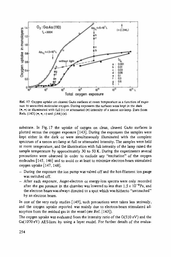
Ref. 17 Oxygen uptake on cleaved GaAs surfaces at room temperature as a function of expo- sure to unexcited molecular oxygen. During exposures the surfaces were kept in the dark (o, m) or illuminated with full (o) or attenuated (~) intensity of a xenon arc-lamp. Data from Refs. 1143] (e, ~, o) and [144] (i).
substrate. In Fig. 17 the uptake of oxygen on clean, cleaved GaAs surfaces is plotted versus the oxygen exposure [143]. During the exposures the samples were kept either in the dark or were simultaneously illuminated with the complete spectrum of a xenon arc-lamp at full or attenuated intensity. The samples were held at room temperature, and the illumination with full intensity of the lamp raised the sample temperature by approximately 30 to 50 K. During the experiments several precautions were observed in order to exclude any "excitation" of the oxygen molecules [ 145, 146] and to avoid or at least to minimize electron-beam stimulated oxygen uptake [ 147,148].
- During the exposure the ion pump was valved off and the hot-filament ion gauge was switched off.
- After each exposure, Auger-electron or energy-loss spectra were only recorded after the gas pressure in the chamber was lowered to less than 1.5 x 10-SPa, and the electron beam was always directed to a spot which was hitherto "untouched" by an electron beam.
In one of the very early studies [ 149], such precautions were taken less seriously, and the oxygen uptake reported was mainly due to electron-beam stimulated ad- sorption from the residual gas in the vessel (see Ref. [ 143]).
The oxygen uptake was evaluated from the intensity ratio of the 0(5 I0 eV) and the Ga(1070 eV) AES-lines by using a layer model. For further details of the evalua-
254

tion the reader is referred to Ref. [ 150]. With increasing exposure the oxygen up- take in the dark tends to saturate below one monolayer. The only other set of data, these results may be compared to, is provided by an XPS investigation of Brundle and Seybold [144]. Their data points are given by the squares in Fig. 17. Consider- ing the approximations entering into the layer model used for the analysis of the experimental AES data and the uncertainties in the estimate of the photoioniza- tion cross-sections used in the evaluation of the x-ray photoemission spectra, both sets of data are in good agreement. Therefore, the more extensive set of our AES- derived data is considered to give the oxygen uptake correctly to within -+ 10 %. Let us first consider the photon-stimulation of the oxygen uptake. The rate, at which molecules impinging on a surface are adsorbed, is determined by the sticking coefficient S which is defined by the relation
dNaa/dt = S �9 dNimp/dt. (12)
Replacing the rate dNimp/dt by the gas pressure p, and measuring the coverage 0 in units of one monolayer Eq. (12) may be written as
d0/dt = c . S . p . (13)
As Fig. 17 shows, the sticking coefficient not only depends on the coverage 0 but also on the intensity of the incident light. The evaluation of the experimental data presented in Fig. 17 gives the intensity dependence of the sticking coefficient as [150]
S(0, I) = S(0, Imax) " I/Imax, (14)
where Ima x is the maximum light-intensity obtained in the present experimental set-up. This relation was found to hold for intensities larger than 0.01 �9 Imax. In- serting this experimentally determined relation into Eq. (13) one obtains
d0/dt = c . S(0, Imax) "P" I/Imax. (15)
This result means that under simultaneous exposure to oxygen molecules and photons the oxygen uptake is controlled by the "combined" exposure p't 'I/Imax. Therefore, the experimental data presented in Fig. 17 are replotted in Fig. 18 as a function of that combined exposure. Evidently, the oxygen uptake under iUumina- tion at both reduced as well as maximum intensities exactly foUows the same curve, excellently confirming Eq. (15).
The data plotted in Fig. 17 have been obtained by simultaneously iUuminating the GaAs surface, which is exposed to oxygen molecules, with the complete spectrum of the xenon lamp. The spectral sensitivity of the stimulation was tested by placing edge filters into the path of light and by using filters with increasing cut-off energy Eco. The experimental results are plotted in Fig. 19, and they show only photons with energies exceeding the band-gap energy of GaAs to stimulate the oxygen up- take. Such photons are creating electron-hole pairs in the semiconductor, and in-
255
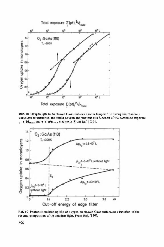
Ref. 18 Oxygen uptake on cleaved GaAs surfaces a room temperature during s imul taneous exposures to unexcited, molecular oxygen and photons as a funct ion of the combined exposure p - t- I /Ima x and p . t . n /nma x (see text). F rom Ref. [1501.
Ref. 19 Photon-st imulated uptake o f oxygen on cleaved GaAs surfaces as a funct ion of the spectral composi t ion o f the incident light. F rom Ref. [150].
2 5 6
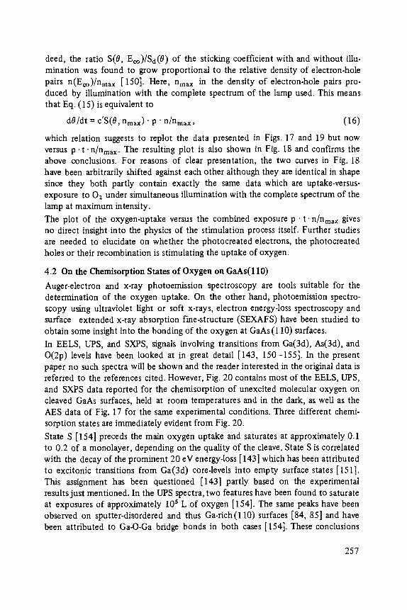
deed, the ratio S(0, Eeo)/Sd(0) of the sticking coefficient with and without illu- mination was found to grow proportional to the relative density of electron-hole pairs n(Eco)/nma x [150]. Here, nma x in the density of electron-hole pairs pro- duced by illumination with the complete spectrum of the lamp used. This means that Eq. (15) is equivalent to
d0/dt = c'S(0, nmax) " p " n/nmax, (16)
which relation suggests to replot the data presented in Figs. 17 and 19 but now versus p. t . n/nmax. The resulting plot is also shown in Fig. 18 and confirms the above conclusions. For reasons of clear presentation, the two curves in Fig. 18 have been arbitrarily shifted against each other although they are identical in shape since they both partly contain exactly the same data which are uptake-versus- exposure to 02 under simultaneous illumination with the complete spectrum of the lamp at maximum intensity.
The plot of the oxygen-uptake versus the combined exposure p - t ' n/nma x gives no direct insight into the physics of the stimulation process itself. Further studies are needed to elucidate on whether the photocreated electrons, the photocreated holes or their recombination is stimulating the uptake of oxygen.
4.2 On the Chemisorption States of Oxygen on GaAs(110)
Auger-electron and x-ray photoemission spectroscopy are tools suitable for the determination of the oxygen uptake. On the other hand, photoemission spectro- scopy using ultraviolet light or soft x-rays, electron energy-loss spectroscopy and surface extended x-ray absorption time-structure (SEXAFS) have been studied to obtain some insight into the bonding of the oxygen at GaAs (110) surfaces.
In EELS, UPS, and SXPS, signals involving transitions from Ga(3d), As(3d), and O(2p) levels have been looked at in great detail [143, 150-155]. In the present paper no such spectra will be shown and the reader interested in the original data is referred to the references cited. However, Fig. 20 contains most of the EELS, UPS, and SXPS data reported for the chemisorption of unexcited molecular oxygen on cleaved GaAs surfaces, held at room temperatures and in the dark, as well as the AES data of Fig. 17 for the same experimental conditions. Three different chemi- sorption states are immediately evident from Fig. 20.
State S [ 154] preceds the main oxygen uptake and saturates at approximately 0.1 to 0.2 of a monolayer, depending on the quality of the cleave. State S is correlated With the decay of the prominent 20 eV energy-loss [ 143] which has been attributed to excitonic transitions from Ga(3d) core-levels into empty surface states [151]. This assignment has been questioned [143] partly based on the experimental results just mentioned. In the UPS spectra, two features have been found to saturate at exposures of approximately 10 s L of oxygen [154]. The same peaks have been observed on sputter-disordered and thus Ga-rich (110) surfaces [84, 85] and have been attributed to Ga-O-Ga bridge bonds in both cases [154]. These conclusions
257
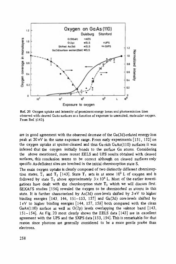
Ref. 20 Oxygen uptake and intensity of prominent energy losses and photoemission lines observed with cleaved GaAs surfaces as a function of exposure to unexcited, molecular oxygen. From Ref. [1431.
are in good agreement with the observed decrease of the Ga(3d)-related energy-loss peak at 20 eV in the same exposure range. From early experiments [151, 152] on the oxygen uptake at sputter-cleaned and thus Ga-rich GaAs(110) surfaces it was inferred that the oxygen initially bonds to the surface Ga atoms. Considering the above mentioned, more recent EELS and UPS results obtained with cleaved surfaces, this conclusion seems to be correct although on cleaved surfaces only specific As-deficient sites are involved in the initial chemisorption state S.
The main oxygen uptake is clearly composed of two distinctly different chemisorp- tion states, T~ and T2 [143]. State T1 sets in at some l0 s L of oxygen and is followed by state T2 above approximately 3 x 10 6 L. Most of the earlier investi- gations have dealt with the chemisorption state T2 which we will discuss first. SEXAFS studies [156] revealed the oxygen to be chemisorbed as atoms in this state. It is further characterized by As(3d) core-levels shifted by 3 eV to higher binding energies [143, 144, 151-153, 157] and Ga(3d) core-levels shifted by 1 eV to higher binding energies [144, 157, 158] both compared with the clean GaAs(110) surface as well as O(2p) levels overlapping the valence band [143, 151-154]. As Fig. 20 most clearly shows the EELS data [143] are in excellent agreement with the UPS and the SXPS data [153, 154]. This is remarkable for that reason since photons are generally considered to be a more gentle probe than electrons.
258

Chemisorption state T1 has escaped detection until recently [ 143]. Spectroscopically it was identified by an O(2p)-related energy-loss of 9 eV which is by 2 eV larger than observed with oxygen chemisorbed in T2. At a temperature of 120 K oxygen is chemisorbed in state Tz only, and the coverage tends to saturate at approximately 0.4 of a monolayer [150]. Illumination, however, was found to stimulate the oxygen uptake beyond that limit. In another recent study [159,160], oxygen was physisorbed on cleaved GaAs surfaces at 45 K or below, and the samples were then warmed up to room temperature. UPS spectra recorded at intermediate tempera- tures discovered a transition state between physisorption and chemisorption in, what we call, state T2. We have identified this "intermediate" state with state T1 for the following reasons. The transition state showed up by an UPS peak shifted by 2 eV to larger binding energies compared to the O(2p)-related peak charac- teristic for atomic oxygen chemisorbed in state T2. This is exactly the same shift in energy as observed by EELS. Based on all the UPS data, the EELS data and the results of a theoretical study [161] the oxygen was proposed [150] to be chemi- sorbed in state T~ as molecules bridging Ga and As atoms belonging to adjacent zig-zag chains of the GaAs(110) surface.
4.3 Chemisorption of Oxygen and Oxidation
The conversion from chemisorption state T1 to T2 also manifests by changes ob- served in the Auger-electron spectra. These data are displayed in Fig. 21 together with the EELS results already shown in Fig. 20. With clean GaAs surfaces two sets of M2M4M4 and MaM4M4 transitions are observed, one for Ga at 50 and 54eV and the other one for As at 36 and 43eV [162]. As displayed in Fig. 21, with increasing oxygen coverage the intensity ratio of each pair of lines initially remains constant but then decreases for coverages above 0.4 of a monolayer. Above this co- verage the shifted As(3d)- and the O(2p)-signals are also observed. The intensity changes in the initial MMM-doublets are caused by the removal of the initial pairs of lines and the build-up of new doublets chemically shifted to lower energies. For Ga it has been observed at 46 and 50eV replacing the original one [150, 163] while the new low-energy line of the As-doublet overlaps the strong M a W arsenic Auger transition at 31 eV. These changes in the Auger-electron spectra again verify the two distinctly different chemisorption states T~ and T2.
As Fig. 21 clearly shows, the transfer of signal strength from the initial into the chemically shifted MMM lines is not altered when the oxygen uptake exceeds the equivalent of one monolayer. However, the curve for the 32 eV arsenic line exhibits a distinct break at a coverage close to one monolayer. This Auger line has been identified as an MaVV arsenic transition in GaAs [ 162]. The existence of this break for the M a W As peak and its absence for both the Ga and As MMM lines in- dicate the formation of a new phase above an uptake equivalent to one monolayer of oxygen. This conclusion implies that only the top layer of the GaAs(110) sur- face is involved in the oxygen-chemisorption state T2 while above a monolayer coverage oxidation of the semiconductor sets in.
259
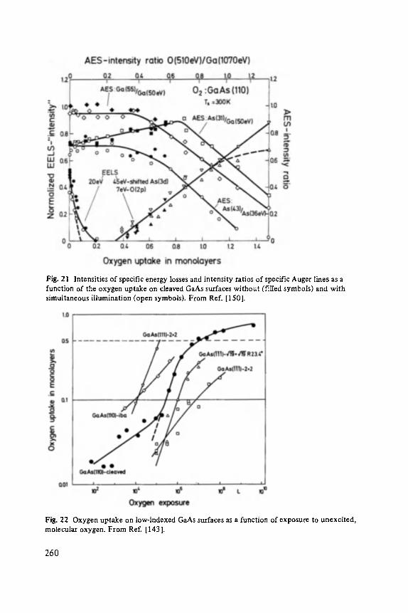
Fig. 21 Intensities of specific energy losses and intensity ratios of specific Auger lines as a function of the oxygen uptake on cleaved GaAs surfaces without (filled symbols) and with simultaneous illumination (open symbols). From Ref. [150].
Fig. 22 Oxygen uptake on low-indexed GaAs surfaces as a function of exposure to unexcited, molecular oxygen. From Ref. [1431.
260
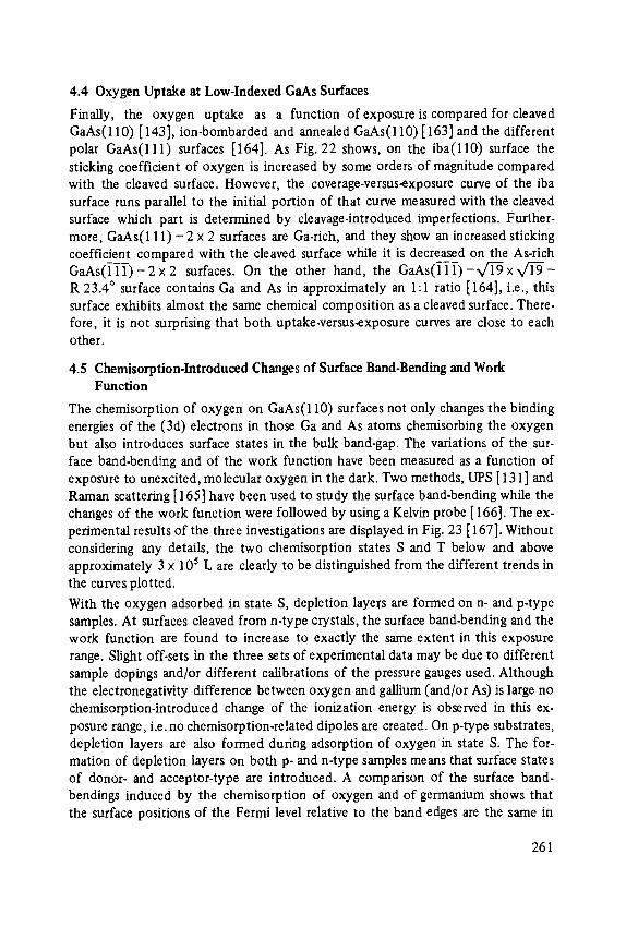
4.4 Oxygen Uptake at Low-Indexed GaAs Surfaces
Finally, the oxygen uptake as a function of exposure is compared for cleaved GaAs(110) [143], ion-bombarded and annealed GaAs(110) [163] and the different polar GaAs(111) surfaces [164]. As Fig. 22 shows, on the iba(l l0) surface the sticking coefficient of oxygen is increased by some orders of magnitude compared with the cleaved surface. However, the coverage-versus-exposure curve of the iba surface runs parallel to the initial portion of that curve measured with the cleaved surface which part is determined by cleavage-introduced imperfections. Further- more, GaAs(111) - 2 x 2 surfaces are Ga-rich, and they show an increased sticking coefficient compared with the cleaved surface while it is decreased on the As-rich G a A s ( l l ] - ) - 2 x 2 surfaces. On the other hand, the G a A s ( l l l - ) - V t ~ x x / ~ - R 23.4 ~ surface contains Ga and As in approximately an 1:1 ratio [ 164], i.e., this surface exhibits almost the same chemical composition as a cleaved surface. There- fore, it is not surprising that both uptake-versus-exposure curves are close to each other.
4.5 Chemisorption-lntroduced Changes of Surface Band-Bending and Work Function
The chemisorption of oxygen on GaAs(110) surfaces not only changes the binding energies of the (3d) electrons in those Ga and As atoms chemisorbing the oxygen but also introduces surface states in the bulk band-gap. The variations of the sur- face band-bending and of the work function have been measured as a function of exposure to unexcited, molecular oxygen in the dark. Two methods, UPS [ 131] and Raman scattering [ 165] have been used to study the surface band-bending while the changes of the work function were followed by using a Kelvin probe [166]. The ex- perimental results of the three investigations are displayed in Fig. 23 [ 167]. Without considering any details, the two chemisorption states S and T below and above approximately 3 x l0 s L are clearly to be distinguished from the different trends in the curves plotted.
With the oxygen adsorbed in state S, depletion layers are formed on n- and p-type samples. At surfaces cleaved from n-type crystals, the surface band-bending and the work function are found to increase to exactly the same extent in this exposure range. Slight off-sets in the three sets of experimental data may be due to different sample dopings and/or different calibrations of the pressure gauges used. Although the electronegativity difference between oxygen and gallium (and/or As) is large no chemisorption-introduced change of the ionization energy is observed in this ex- posure range, i.e. no chemisorption-related dipoles are created. On p-type substrates, depletion layers are also formed during adsorption of oxygen in state S. The for- mation of depletion layers on both p- and n-type samples means that surface states of donor- and acceptor-type are introduced. A comparison of the surface band- bendings induced by the chemisorption of oxygen and of germanium shows that the surface positions of the Fermi level relative to the band edges are the same in
261
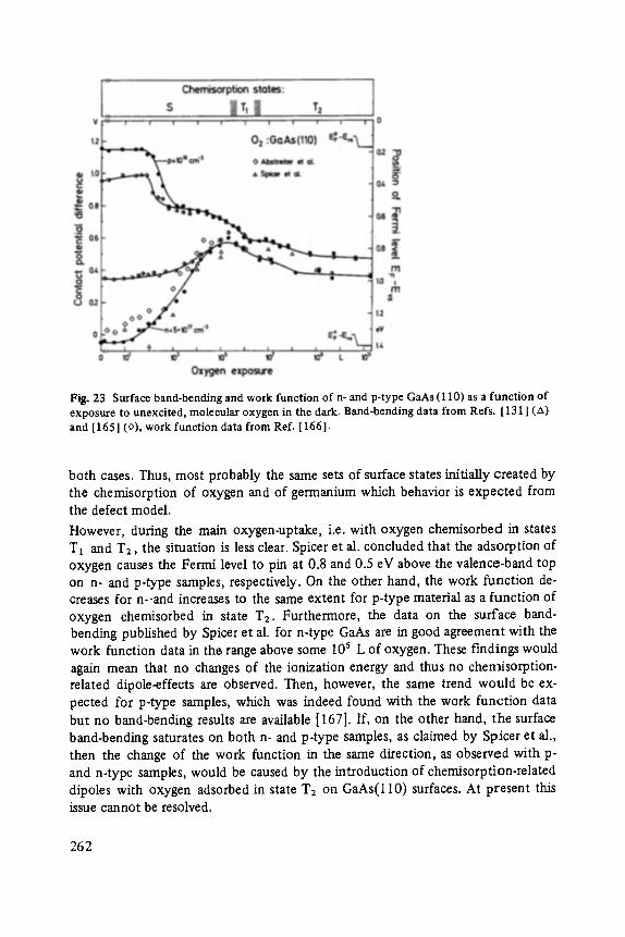
Fig. 23 Surface band-bending and work function of n- and p-type GaAs (110) as a function of exposure to unexcited, molecular oxygen in the dark. Band-bending data from Refs. [1311 (a) and [ 1651 (o), work function data from Ref. [ 166 l-
both cases. Thus, most probably the same sets of surface states initially created by the chemisorption of oxygen and of germanium which behavior is expected from the defect model.
However, during the main oxygen-uptake, i.e. with oxygen chemisorbed in states T~ and T2, the situation is less clear. Spicer et al. concluded that the adsorption of oxygen causes the Fermi level to pin at 0.8 and 0.5 eV above the valence-band top on n- and p-type samples, respectively. On the other hand, the work function de- creases for n--and increases to the same extent for p-type material as a function of oxygen chemisorbed in state T2. Furthermore, the data on the surface band- bending published by Spicer et al. for n-type GaAs are in good agreement with the work function data in tho range above some l0 s L of oxygen. These findings would again mean that no changes of the ionization energy and thus no chernisorption- related dipole-effects are observed. Then, however, the same trend would be ex- pected for p-type samples, which was indeed found with the work function data but no band-bending results are available [167]. If, on the other hand, the surface band-bending saturates on both n- and p-type samples, as claimed by Spicer et al., then the change of the work function in the same direction, as observed with p- and n-type samples, would be caused by the introduction of chemisorption-related dipoles with oxygen adsorbed in state T2 on GaAs(110) surfaces. At present this issue cannot be resolved.
262
5 Final Remarks
In the preceding, I have tried to focus on some of the topics currently discussed with III-V compound-semiconductor surfaces and interfaces. As pointed out in the introduction, their selection was partly motivated by my own research interests. My intentions have been not only to present remits and interpretations everybody active in the field agrees upon, but also to discuss some of the open or seemingly solved problems where further work is needed. To my opinion, future investiga- tions should utilize and develop experimental tools that are probing the surface properties in areas well below the usual 1 mm in diameter, and they should con- sider the simultaneous application of more than one experimental technique.
Acknowledgements
The author should like to acknowledge the many fruitful discussions with Dr. Chadi, Dr. Ludeke, and Professor Spicer and his students. Furthermore, he has to thank Dr. Abstreiter for supply- ing some of his results prior to publication. The manuscript was typed by A. Kohs, and the drawings were prepared by J. Krusenbaum. The experimental studies in Duisburg were supported by grants from the Deutsche Forschungsgemeinschaft and from the Minister ftir Wissenschaft und Forschung des Landes Nordrhein-Wesffalen.
References
[1] H. Welker, Z. Naturforsch. 7a, 744 (1952). [2] A. Onton, in Festk6rperprobleme: Advances in Solid State Physics, edited by
H. J. Queisser (Vieweg, Braunschweig, 1973), Vol. XIII, p. 59. C3] P. R. Selway, A. R. Goodwin, and G. H. B. Thompson, in Festk6rperprobleme:
Advances in Solid State Physics, edited by H.J. Queisser (Vieweg, Braunschweig, 1974), Vol. XIV, p. 119.
[4] R. Dingle, in Festk6rperprobleme: Advances in Solid State Physics, edited by H. Z Queisser (Vieweg, Braunschweig, 1975), Vol. XV, p. 21.
[5] H. Beneking, in Festk6rperprobleme: Advances in Solid State Physics, edited by J. Treusch (Vieweg, Braunschweig, 1976), Vol. XVI, p. 195.
[6] L.F. Eastman, in Festk6rperprobleme: Advances in Solid State Physics, edited by P. Grosse (Vieweg, Braunschweig, 1982), Vol. XXII, p. 173.
[7] N.T . Linh, in FestkSrperprobleme: Advances in Solid State Physics, edited by P. Grosse (Vieweg, Braunschweig, 1983), Vol. XXIII, p. 227.
[8] A. Schlachetzki, in FestkSrperprobleme: Advances in Solid State Physics, edited by P. Grosse (Vieweg, Braunschweig, 1983), Vol. XXIII, p. 295.
[9] K. Heime, in Festk6rperprobleme: Advances in Solid State Physics, edited by P. Grosse (Vieweg, Braunschweig, 1984), Vol. XXIV, p. 311.
[10] F. Capasso, Surface Sci. 132,527 (1983). [11] H. Kroemer, Japan. J. Appl. Phys. 20 Supplement 1, 9 (1981). [12] L.J. Brillson, Surface Sci. Rep. 2, 123 (1982).
263
[13] See J. Vac. Sci. Technol. 13(4) (1976); 14(4) (1977); 15(4) (1978); 16(4) (1979); 17(5) (1980); 19(3) (1981); 21(2) (1982); BI (3) (1983); B2 (1984).
[14] A.E . MacRae and G. W. Gobeli, in Semiconductors and Semimetals ed. by R. K. Willardson and A. C. Beer (Academic Press, New York, 1966), Vol. 2, p. 115.
[15] J. van Laar and Z J. Scheer, Surface Sei. 8, 343 (1967). [16] A. Hui/ser and J. van Laar, Surface Sci. 52, 202 (1975). [17] W. Gudat, D. E. Eastman and .I.J. Freeouf, J. Vac. Sci. Technol. 13, 250 (1976).
[18] W. E. Spicer, L Lindau, P. E. Gregory, C. M. Garner, P. Pianetta and P. I~. Chye, J. Vac. Sci. Technol. 13,780 (1976).
[19] H. Z Clemens and W. M6nch, J. Vac. Sci. Technol. 16, 1238 (1979). [201 Z van Laar, A. Huijser, and T. L. van Rooy, J. Vac. Sci. Technol. 14, 894 (1977).
[21] A. Huijser, J. van Laar, and T. L. van Rooy, Surface Sei. 62, 472 (1977). [22] J.D. Joannopoulos and M. L. Cohen, Phys. Rev. BI0, 5075 (1974).
[23] C. Calandra and G. Santoro, J. Phys. C: Solid State Phys. 8, L86 (1975). [24] J .R. Chelikowski, S. G. Louie, and M. L. Cohen, Phys. Rev. B14, 4726 (1976).
[25] D.J. Chadi, Phys. Rev. B18, 1800 (1978). [26] K.C. Pandey, J. Vac. Sei. Technol. 15,440 (1978). [27] F. Manghi, C. M. Bertoni, C. Calandra, and E. Molinari, Phys. Rev. B24, 6029 (1981).
[28] J .A . Knapp and G. J. Lapeyre, J. Vac. Sci. TechnoL 13, 757 (1976). [29] G.P. Williams, R. J. Smith, and G. J. Lapeyre, J. Vac. Sci. TechnoL 15, 1249 (1978). [30] A. Huijser, J. pan Laar, and T. L. van Rooy, Phys. Lett. 65A, 337 (1978). [31 ] V. Dose, H.-J. Gossmann, and D. Straub, Phys. Rev. Lett. 47,608 (1981), Surface Sci.
117,387 (1982). [32] C.B. Duke, J. Vac. Sci. Technol. BI, 732 (1983). [33] A. Kahn, Surface Sci. Rep. 3, 193 (1983). [34] D. Haneman, Phys. Rev. 121, 1093 (1961). [35] A. Taloni and D. Haneman, Surface Sci. 10,215 (1968). [36] D. E. Eastman, T. C. Chiang, P. Heimann, and F.J. HimpseI, Phys. Rev. Lett. 45
(1980) 656. [37] M. Taniguchi, S. Suga, M. SekL S. Shin, K. L. I. Kobayashi, and H. Kanzaki, J. Phys. C:
Solid State Phys. 16, L45 (1983). [38] A. Many, Y. GoMstein, and N. B. Grover, Semiconductor Surfaces (North-Holland,
Amsterdam, 1965). [39] D. Frankl, Electrical Properties of Semiconductor Surfaces (Pergamon, Oxford, 1967). [40] W. M6nch, R. Enninghorst, and H. J. Clemens, Surface Sci. Lett. 102, L54 (1981). [41] L. Koenders and ~r M6nch, Verhandl. DPG (VI) 19, 170 (1984).
[42] Sir 1u Thomson, Nature 23, 567 (1881). [43] C. H. Gatos, J. J. Iraughan, J. Lagowski, and H. C. Gatos, J. Appl. Phys. 52, 1464
(1981). [44] M. Skibowski, G. Spriissel, and V. Saile, Appl. Opt. 19, 3978 (1980). [45] D.E. Aspnes, C. G. Olson, and D. I~. Lynch, Phys. Rev. Lett. 36, 1563 (1976).
[46] M.B. Panish and H. C. Casey, J. Appl. Phys. 40 (1969) 163.
[47] D.E. Aspnes, Phys. Rev. B14, 5331 (1976).
264

[48] S.C. Yu and H. Brooks, unpublished. [49] H. Y. Fan, Phys. Rev. 82, 900 (1951). [50] Z Camassel and D. Auvergne, Phys. Rev. BI2, 3258 (1975). [51] K. Baumann, phys. stat. sol. (b)63, K71 (1974). [52] Iv.A. Harrison, Electronic Structure and the Properties of Solids (Freeman,
San Francisco, 1980). [53] IV. A. Harrison, in Festk6rperprobleme: Advances in Solid State Physics, edited by
J. Treusch (Vieweg, Braunschweig, 1977), Vol. XVII, p. 135. [54] D.J. Chadi and M. L. Cohen, phys. stat. sol. (b) 68, 405 (1975). [55] F. Herman and S. Skillman, Atomic Structure Calculations, (Prentice Hall, Englewood
Cliffs, N. J., 1963). [56] J.J. Lander, G. IV. Gobeli, and,/. Morrison, J. Appl. Phys. 34, 2298 (1963). [57] G. IV. Gobeli and F. G. Allen, Phys. Rev. 137, A 245 (1965). [58] T.E. Fischer, Phys. Rev. 139, A 1228 (1965). [59] R.K. Swank, Phys. Rev. 153,844 (1967). [60] G. 1t4. Guichar, C.A. Sebenne, and C. D. Thuault, in Proc. 3rd Intl. Conf. Solid Surf.,
edited by R. Dobrozemsky, F. Riidenauer, F. P. Vieb6ck, andA. Breth, (Vienna, 1977) p. 623.
[61] J. van Laar, A. Hui/ser, and T. L. van Rooy, J. Vac. Sci. Technol. 14, 894 (1977). [62] G.M. Guichar, C. A. Sebenne, and C. D. Thuaulr, Surf. Sci. 86, 789 (1979). [63] IV. M6nch andP. P. Auer, J. Vac. Sci. Technol. 15, 1230 (1978). [64] R. Feder, IV. M6nch, and P. P. Auer, J. Phys. C: SoLid State Phys. 12, L179 (1979).
[65] K, C. Pandey, Phys. Rev. Lett. 47, 1913 (1981); Physica I17B & II8B, 761 (1983). [66] R.M. Tromp, L. Stair, andJ. F. van der Veen, Phys. Rev. Lett. 51, 1672 (1983). [67] P. Chiaradia, A. Cricent~', S. Selei, and G. Chiarotti, Phys. Rev. Lett. 52, 1145 (1984). [68] M.A. Olmstead andN. M. Amer, Phys. Rev. Lett. 52, 1148 (1984). [69] R. Federand IV. M6nch, SoLid State Commun. 50, 311 (1984).
[70] R. Smoluchowski, Phys. Rev. 60,661 (1941). [71] P. O. Gartland, S. Berge, and B. J. Slagsvold, Physica Norvegica 7, 39 (1973). [72] M. Chelvayohan and C. H. B. Mee, J. Phys. C: Solid State Phys. 15, 2305 (1982). [73] J.R. Arthur, Surface Sci. 43, 449 (1974). [74] A.J. van Bommel, J. E. Crombeen, and T. G. J. van Oirschot, Surface Sci. 72, 95
(1978). [75] P. Drathen, IV. Ranke, and K. Jacobi, Surface Sci. 77, L 162 (1978). [76] J. Massies, P. Etienne, F. Delzaly, and N. T. Linh, Surface Sci. 99, 121 (1980). [77] R.Z . Bachrach, R. S. Bauer, P. Chiaradia, and G. It'. Hansson, J. Vac. Sci. Technol.
19,335 (1981). [78] S. P. Svensson, J. Kanski, T. G. Andersson, and P. O. Nilsson, Surface Sci. 124, L31
(1983). [79] A.D. Katnani, H. IV. Sang, jr., and R. S. Bauer. J. Vac. Sci. Technol. B2, in press
(1984). [80] J.F. vanderVeen, L. Smit, P.K. Larsen, and J.H. Neave, Physica l l7B&II8B,
822 (1983). [81] IV. Ranke, Phys. Rev. B27, 7807 (1983).
265
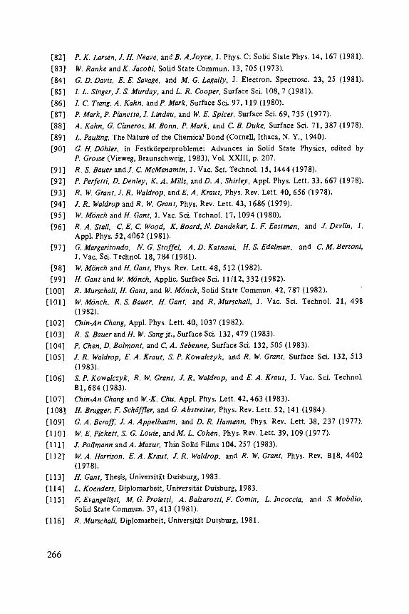
[82] [83] [84] [85] [86] [87] [88] [89] [90]
[91]
[92] [93]
[94]
[95]
[96]
[97]
[98] [99]
[100] [101]
[102] [103] [104] [105]
[106]
[107] [108] [109]
[110]
[111]
[112]
[113] [114]
[115]
[116]
P. K. Larsen, J. H. Neave, andB. A.Joyce, J. Phys. C: Solid State Phys. 14, I67 (1981).
W. Ranke and K. Jacobi, Solid State Commun. 13, 705 (1973).
G. D. Davis, E. E. Savage, and M. G. Lagally, J. Electron. Spectrosc. 23, 25 (!981).
1. L. Singer, J. S. Murday, and L. R. Cooper, Surface Sci. 108, 7 (1981).
I. C. Tsang, A. Kahn, and/'. Mark, Surface Set. 97, 119 (1980).
P. Mark, P. Pianetta, I. Lindau, and W. E. Spicer, Surface Sci. 69, 735 (1977).
A. Kahn, G. Cisneros, M. Bonn, P. Mark, and C. B. Duke, Surface Sci. 71,387 (1978).
L. Pauling, The Nature of the Chemical Bond (CorneU, Ithaca, N. Y., 1940).
G. H. Dohler, in Festk6rperprobleme: Advances in Solid State Physics, edited by P. Grosse (Vieweg, Braunschweig, 1983), Vol. XXIII, p. 207.
R. S. Bauer andJ. C. McMenamin, J. Vac. Sci. Technol. 15, 1444 (1978).
P. Perfetti, D. Denley, K. A. Mills, andD. A. Shirley, Appl. Phys. Lett. 33,667 (1978).
R. W. Grant, J. R. Waldrop, andE. A. Kraut, Phys. Rev. Lett. 40, 656 (1978).
J. R. Waldrop andR. W. Grant, Phys. Rev. Lett. 43, 1686 (1979).
W. M6nch andH. Gant, J. Vac. Sci. Technol. 17, 1094 (1980).
R. A. Stall, C. E. C. Wood, K. Board, N. Dandekar, L. F. Eastman, and J. Devlin, J. Appl. Phys. 52, 4062 (1981). G. Margaritondo, N. G. Stoffel, A. D. Katnan4 H. S. Edelman, and C. M. Berton4 1. Vac. Sci. Technol. 18,784 (1981).
W. M6nch andH. Gant, Phys. Rev. Lett. 48,512 (1982).
H. Gant and W. M6nch, Applic. Surface Sci. 11/12, 332 (1982).
R. Murschall, H. Gant, and W. M6nch, Solid State Commun. 42,787 (1982).
W. M6nch, R. S. Bauer, H. Gant, and R. Murschall, J. Vac. Set. Technol. 21, 498 (1982). Chin-An Chang, Appl. Phys. Lett. 40, 1037 (1982).
R. S. Bauer and H. W. Sang jr., Surface Set. 132,479 (1983).
P. Chen, D. Bolmont, and C. A. Sebenne, Surface Set. 132, 505 (1983).
J. R. Waldrop, E. A. Kraut, S. P. Kowalczyk, and R. W. Grant, Surface Sci. 132, 513 (1983). S. P. Kowalczyk, R. W. Grant, J. R. Waldrop, and E. A. Kraut, J. Vac. Sci. Technol. BI, 684 (1983).
Chin.An Chang and W.-K. Chu, Appl. Phys. Lett. 42, 463 (1983). H. Brugger, F. Schaffler, and G. Abstreiter, Phys. Rev. Lett. 52, 141 (1984).
G. A. Baraff, J. A. Appelbaum, and D. R. Hamann. Phys. Rev. Lett. 38, 237 (1977).
W. E. Pickett, S. G. Louie, andM. L. Cohen, Phys. Rev. Lett. 39, 109 (1977).
J. Pollmann andA. Mazur, Thin Solid Films 104, 257 (1983).
W. A. Harrison, E. A. Kraut, J. R. Waldrop, and R. W. Grant, Phys. Rev. B18, 4402 (1978). 1t. Gant, Thesis, Universit~it Duisburg, 1983.
L. Koenders, Diplomarbeit, Universit~t Duisburg, 1983.
17. Evangelisti, M. G. Proietti, A. Balzarotti, F. Comin, L. lncoccia, and S. Mobilio, Solid State Commun. 37, 413 (1981).
R. Murschall, Diplomarbeit, Universit~t Duisburg, 1981.
266
[117] [118] [119] [120] [121] [122] [123]
[124]
[125]
[126] [127]
[128]
[129]
[130] [131] [132]
[133] [134] [135]
[136] [137] [138] [139] [140]
[141] [142]
[143]
[144] [145] [146] [147] [148] [149]
H. Gant and W. MOnch, Surface Sci. 105,217 (1981). H. IV. Etzkorn and J. Kirschner, Nucl. Instrum. Meth. 168, 395 (1980). M. Hansen, Constitution of Binary Alloys (McGraw Hill, New York, 1958).
F. Bartels, H. J. Clemens, and W. M6nch, Physica II7B & II8B, 801 (1983). H. Gant, L. Koenders, F. Bartels, and IV. MOnch, Appl. Phys. Lett. 43, 1032 (1983). H. Ullrich and W. MOnch, unpublished. O. Kubaschewski and C. B. Alcock, Metallurgical Thermochemistry (Pergamon, Oxford, 1979). H. Kroemer, Proc. 2rid Course of the Intl. School on Solid-State Device Research, edited by L. L. Chang and K. Ploog (Nijhoff, The Hague, in print). IV. M6nch, in "Physics of Submicron Semiconductor Devices", edited by H. Grubin (Plenum, New York 1984) in press.
IV. MOnch, Surface Sci. 132, 92 (1983). IV. E. Spice& P. IV. Chye, P. R. Skeath, C. Y. Su, and L Lindau, J. Vac. Sci. Technol. 16, 1422 (1979). IV. E. Spicer, I. Lindau, P. Pianetta, P. IV. Chye, and C. M. Garner, Thin Solid Films 56, 1 (1979). P. Skeath, L Lindau, P. IV. Chye, C. Y. Su, and IV. E. Spicer, J. Vae. Sci. TechnoL 16, 1143 (1979). IV. M6nch, Thin Solid Films 104, 285 (1983). IV. E. Spicer, L Lindau, P. Skeath, and S. Y. Su, J. Vac. Sci. Technol. 17, 1019 (1980). IV. E. Spicer, P. Skeath, C. Y. Su, and L Lindau, J. Phys. Soe. Japan 49, Suppl. A, 1079 (1980). M. S. Daw andD. L. Smith, Phys. Rev. B20,515 (1979). M. S. Daw andD. L. Smith, Appl. Phys. Lett. 36, 690 (1980), M. S. Daw andD. L. Smith, Solid State Commun. 37,205 (1981). R. E. Allen andJ. E. Dow, J. Vac. Sci. Technot 19,383 (1981). R. E. Allen andJ. E. Dow, AppL Surface Sci. 11/12, 362 (1982). R. E. Allen and,/. E. Dow, Phys. Rev. B25, 1423 (1982).
D. V. Lang, Inst. Phys. Conf. Ser. 31, 70 (1977). IV.M6nch, in "Chemistry and Physics of Solid Surfaces", Vol. 5, edited by R. Vanselow and R. Howe(Springer Series in Chemical Physics, VoL 35) (Springer, Berlin, 1984) in press. R. IV6rner, U. Kaufmann, andJ. Schneider, Appl. Phys. Lett. 40, 141 (1982). E. R. IVeber, H. Ennen, U. Kaufmann, J. IVindscheid, and J. Schneider, J. AppL Phys. 53, 6140 (1982). F. Bartelx, L. Surkamp, H. J. Clemens, and IV. M6nch, J. Vac. Sci. Technol. BI, 756 (1983). C. R. Brundle andD. Seybold, J. Vac. Sei. Technol. 16, 1186 (1979). R. J. Archer and IV. Gobeli, J. Phys. Chem. Solids 26,343 (1965). P. Pianetta, L Lindau, C.M. Garner, and IV. E. Spicer, Phys. Rev. B18, 2792 (1978). H. [bach, K. Horn, R. Dorn, and H. Lath, Surface Sci. 38,433 (1973). IV. Ranke and K. Jacobi, Surface Sci. 47,525 (1975). R. Dorn, H. Lath, and G. J. Russell, Phys. Rev. BI0, 5049 (1974).
267
[1501 [151] [152] [153]
[1541
[1551
[156]
[157]
[158]
[159]
[160] [1611 [162] [163] [164] [165] [166] [167]
F. Barrels and W. M6nch. Surface SO. in press.
R. Ludeke andA. Korea, J. Vac. Sci. Technol. 13, 241 (1976).
R. Ludeke, SoLid State Commun. 21,815 (1977).
1'. Pianetta, L Lindau, C. Garner, and W. E. Spieer, Phys. Rev. Lett. 35, 1356 (1975). Phys. Rev. Lett. 37, 1166 (1976).
C. Y. Su, I. Lindau, P. W. Chye, P. Skeath, and IV. E. Spice& Phys. Rev. B25, 4045 (1982).
141. E. Spicer, P. Pianetta, 1. Lindau, and P. W. Chye, J. Vac. Sci. Technol. 16, 1191 (1979).
J. St6hr, R. 8. Bauer, J. C. McMenamin, L. L Johansson, and S. Brennan, J. Vac. Sci. Technol. 16, 1195 (1979).
H. Iwasaki, Y. Mizokawa, R. Nishitani, and S. Nakamura, Japan. J. Appl. Phys. 17, 315 (1978).
t'. IV. Chey, C. I". Su, L Lindau, P. Skeath, and IV. E. Spicer, J. Vae. Sci. Technol. 16, 1191 (1979).
D. J. Frankel, Y. Yukun, R. Avici, and G. J. Lapeyre, J. Vac. Sci. Technol. A1, 679 (1983).
D. J. Frankel, J. R. Anderson, and G. J. Lapeyre, J. Vac. Sci. Technol. B1,763 (1983).
E. J. Mele and,/. D. Joannopoulos, Phys. Rev. B18, 6999 (1978).
J. Z Uebbing andN. J. Taylor, J. Appl. Phys. 41 ,804 (1970).
IV. Ranke, Y. R. Xing, and G. D. Shen, Surface Sci. 122, 256 (1982).
IV. Ranke and K. Jacobi, Surface Sci. 63, 33 (1977).
G. Ab~treiter and F. Sehaffler, private communication.
F. Barrels and IV. M6nch, VerhandL DPG (VI)/9, 170 (1984).
The data of the surface band-bending reported in Ref. [131] for p-type sample have been measured as a function of excited oxygen and shall thus not be considered here.
268

Festk6rperproblerne XXIV (1984)
High Resolution Sputter Depth Profiling of Solid Interfaces and Thin Film Structures
Hans Oechsner Fachbereich Physik tier Universit~t Kaiserslautern, Kaiserslautern, Federal Republic of Germany
Summary: Controlled sputter removal of a sample in conjunction with a surface analytical technique has proved to be the most sensitive method for the chemical analysis of concentra- tion profiles in solids and concentration transitions at thin film interfaces. Apart from the quantitative correlation between the analytical signals and the concentration values, high depth resolution is the most important requirement for sputter depth profiling. Experimentally manageable as well as principally unavoidable effects influencing depth resolution are discussed. In particular, low ion bombarding energies are shown to be necessary for minimizing the depth of sputter induced stoichiometry changes. Because of its high quantificability the low energy mode of Secondary Neutral Mass Spectro- metry SNMS is found to be very appropriate for high resolution depth profiling. When the in- fluences of unavoidable physical effects are taken into account, atomically sharp interfaces can be identified. Examples for depth profiling by low energy SNMS with extremely high depth resolution are presented.
1 I n t r o d u c t i o n
A decisive step forward for the chemical analysis of concentration depth profiles in solids and of the concentration transitions at the interfaces of thin film systems has been made by combining surface analytical methods with controlled sputter removal of the specimens. As the information depth of the physical methods for surface analysis is in the order of one or several atomic distances, and as particle removal by sputtering occurs on an atomic scale, sputter depth profiling in con- junction with a surface sensitive analytical technique is supposed to be an almost ideal method for chemical analysis of concentration profiles and interfaces with extremely high depth resolution.
The surface analytical methods employed for such purposes can be divided into two categories. In the first one, atoms or molecules being removed from the surface by ion bombardment are characterized by mass spectrometric techniques or optical spectroscopy. Such methods are referred to as Secondary Ion or Secondary Neutral Mass Spectrometry, SIMS [1] or SNMS [2], and as Glow Discharge Optical Spectro- scopy GDOS [3]. For depth profiling with such techniques the ion bombardment of the sample is used for the excitation of the analysed particles and at the same time for carrying off the sample material.
269
The second group of methods comprises the energy analysis of Auger electrons (Auger Electron Spectroscopy AES [4]) and of photoelectrons (mainly X-ray induced Photoelectron Spectroscopy XPS [5]) emitted from the outermost atomic layers of a solid. In conjunction with sputter depth profiling these methods are monitoring what is left at the surface. Hence, the two categories of surface analyti- cal techniques are complementary to each other.
It is, however, well-known from recent measurements [6, 7] that the ion bombard- ment causes in general sometimes drastic changes of the composition of the upper- most atomic layers via atomic displacement processes in the sputtering cascades and different emission probabilities for different species. Thus, as soon as sputtering is involved in the analysis of a solid, both groups of surface analytic techniques are expected to give different information about the composition of the actual surface just laid open during sputter depth prof'fling. Hence, the mass spectrometric methods which are collecting those particles being removed from the sample seem to be of some advantage, at least under stationary conditions. On the other hand, informa- tion about the chemical state of the particles at the investigated surface can be supplied directly by the electron spectroscopic techniques AES and XPS.
Apart from the quantitative correlation between the analytical signals and the original sample composition, high depth resolution is the most important point in concentration depth prof'fling. A depth resolution as high as possible becomes in- creasingly necessary in particular with respect to the continuous increase of mini- aturization, i.e. the decrease of the individual layer thicknesses in thin trim systems. Though sputter depth profiling in combination with a surface sensitive analytical technique is in principle very promising in this context, the practical performance of such measurements has revealed the existence of a number of effects which are limiting the experimentally obtainable depth resolution [7]. These effects may be again divided in two groups, namely in such interfering influences which can be minimized by experimental measures and, secondly, in processes of fundamental nature which arise from the physical character of the sputtering effect itself and which, therefore, establish an unavoidable lower limit for experimental depth resolution. In the following sections the two groups of limiting effects are discussed in detail. Simultaneously, experimental and theoretical methods are described by which such effects can be eliminated or corrected. Subsequently, some practical examples for depth profile analysis with extremely high depth resolution will be given.
Before doing so, the term "depth resolution" has to be clarified. In Fig. la an example for the Final goal of a depth profile analysis is sketched, namely the varia- tion of the concentrations cl and c2 of two components across an interface in a thin film system. In the following we take as depth resolution the smallest depth interval 8z for which the values of ct(z) and c2(z) at a depth z can be safely deter- mined by the depth profiling measurement. This definition differs from the absolute or relative "depth resolution" Az or Az/z, taking Az as the distance along which the
270
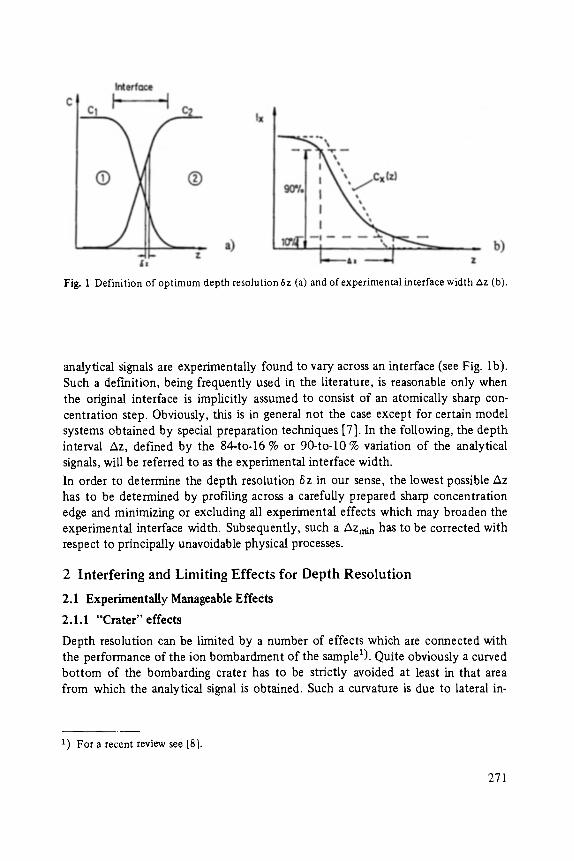
Fig. 1 Definition of optimum depth resolution 6 z (a) and of experimental interface width Az (b).
analytical signals are experimentally found to vary across an interface (see Fig. lb). Such a definition, being frequently used in the literature, is reasonable only when the original interface is implicitly assumed to consist of an atomically sharp con- centration step. Obviously, this is in general not the case except for certain model systems obtained by special preparation techniques [71. In the following, the depth interval Az, defined by the 84-to-16 % or 90-to-10 % variation of the analytical signals, will be referred to as the experimental interface width.
In order to determine the depth resolution fiz in our sense, the lowest possible Az has to be determined by profiling across a carefully prepared sharp concentration edge and minimizing or excluding all experimental effects which may broaden the experimental interface width. Subsequently, such a AZmt, has to be corrected with respect to principally unavoidable physical processes.
2 In t e r f e r ing and Limi t ing Ef fec t s for Dep th R e s o l u t i o n
2.1 Experimentally Manageable Effects
2.1.1 "Crater" effects
Depth resolution can be limited by a number of effects which are connected with the performance of the ion bombardment of the sample~). Quite obviously a curved bottom of the bombarding crater has to be strictly avoided at least in that area from which the analytical signal is obtained. Such a curvature is due to lateral in-
1) For a recent review see [8].
271
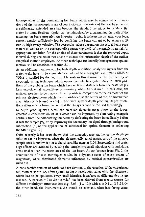
homogeneities of the bombarding ion beam which may be connected with varia- tions of the macroscopic angle of ion incidence. Rastering of the ion beam across a sufficiently extended area has become the standard technique to produce flat crater bottoms. Residual ripples can be minimized by programming the path of the rastering ion beam properly. An important point is to keep the instantaneous local current density sufficiently low by conf'ming the beam current or by using a suffi- ciently high sweep velocity. The respective values depend on the actual beam para- meters as well as on the corresponding sputtering yield of the sample material. An appropriate condition for the choice of these parameters is that the removed depth interval during one raster run does not exceed the information depth of the surface analytical method employed. Another technique for laterally homogeneous sputter removal will be described in section 3.1. As an additional requirement for high depth resolution, analytical signals from the crater wails have to be eliminated or reduced to a negligible level. When SIMS or SNMS is applied for the depth profile analysis this demand can be fulfilled by an electronic gating technique which opens the detecting system only for such posi- tions of the probing ion beam which have sufficient distances from the crater edges. Less experimental expenditure is necessary when AES is used. In this case, the rastered area has to be made sufficiently wide in comparison to the diameter of the primary electron beam which then is positioned at the center of the ion bombarded area. When XPS is used in conjunction with sputter depth profiling, depth resolu- tion suffers mostly from the fact that the X-rays cannot be focused accordingly.
In depth profiling with SIMS the so-called dynamic range down to the lowest detectable concentration of an element can be improved by eliminating energetic neutrals from the bombarding ion beam by deflecting the beam immediately before it hits the sample [9], or by improving the secondary ion signal through background subtraction [8] or the application of additional ion optical elements in collecting the SIMS signal [9].
Quite recently it has been shown that the dynamic range and hence the depth re- solution can be improved when the electronically gated central part of the rastered sample area is subdivided in a chessboard-like manner [10]. Surrounding and crater edge effects are avoided by cutting the sample into small minichips with individual areas smaller than the raster area of the ion beam. As can be seen from Fig. 2, the combination of these techniques results in a dynamic range of seven orders of magnitude, when chessboard elements influenced by residual contamination are ruled out.
A considerable amount of work has been devoted to the question, if the experimen- tal interface width Az, often quoted as depth resolution, varies with the distance z which has to be sputtered away until identical interfaces at different depths are reached. A behaviour like Az = a +/3z n has been derived from measurements for different multilayer structures (see e.g. Refs. [11, 12]) with n "-- 0,5 ... 1 [13]. On the other hand, the instrumental Az should be constant, when interfering crater
272
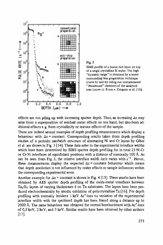
Fig. 2 SIMS profile of a boron rich layer on top of a single crystalline Si wafer. The high "dynamic range" is obtained by a novel surrounding free preparation technique (curve b) and by ruling out contaminated "chessboard" elements of the analysed area (curve c). From v. Criegern et al. [101.
effects are not piling up with increasing sputter depth. Thus, an increasing Az may arise from a superposition of residual crater effects on one hand, but also from ad- ditional effects e.g. from crystallinity or texture effects of the sample.
There are indeed several examples of depth profiling measurements which display a behaviour with Az = constant. Corresponding results taken from depth profiling studies of a periodic sandwich structure of alternating Ni and Cr layers by Giber et al. are shown in Fig. 3 [14]. These data refer to the experimental interface widths which have been determined by SIMS sputter depth profiling for in total 23 Ni-Cr or Cr-Ni interfaces of equidistant positions with a distance of nominally 100 A. As can be seen from Fig. 3, the relative interface width Az/z varies with z -1 . Hence, these measurements display the expected Az = constant behaviour which means that depth resolution is not influenced by crater effects or sample influences within the corresponding experimental error.
Another example for Az = constant is shown in Fig. 4 [15]. These results have been obtained by AES sputter depth profiling of the oxide-metal interfaces between Ta2Os layers of varying thicknesses d on Ta substrates. The layers have been pro- duced electrochemically by anodic oxidation of polycrystalline Ta [ 16]. For depth profiling with normally incident 1 keV Ar*-ions no variation of the experimental interface width with the sputtered depth has been found along a distance up to 2000 )k. The same behaviour was obtained for normal bombardment with Ar+-ions of 0,5 keV, 2 keV, and 3 keV. Similar results have been obtained by other authors [17].
273
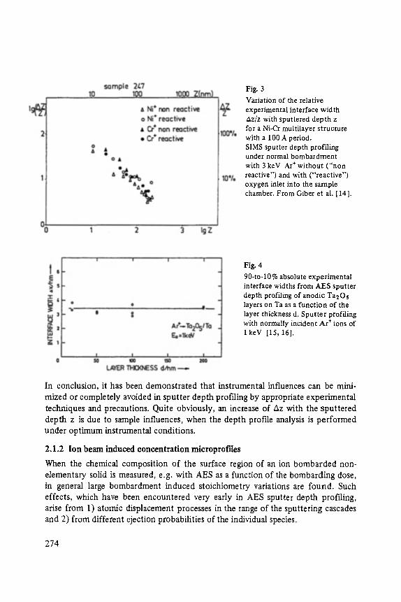
Fig. 3 Variation of the relative experimental interface width Az/z with sputtered depth z for a Ni-Cr multilayer structure with a 100 A period. SIMS sputter depth profiling under normal bombardment with 3 keV Ar § without ("non reactive") and with ("reactive") oxygen inlet into the sample chamber. From Giber et al. [14].
Fig. 4 90-to-i0% absolute experimental interface widths from AES sputter depth proftling of anodic Ta205 layers on Ta as a function of the layer thickness d. Sputter profiling with normally incident Ar* ions of 1 key [15, 16].
In conclusion, it has been demonstrated that instrumental influences can be mini- mized or completely avoided in sputter depth profiling by appropriate experirnental techniques and precautions. Quite obviously, an increase of Az with the sputtered depth z is due to sample influences, when the depth profile analysis is performed under optimum instrumental conditions.
2.1.2 Ion beam induced concentration mieroprof'fles
When the chemical composition o f the surface region of an ion bombarded non- elementary solid is measured, e.g. with AES as a function of the bombarding dose, in general large bombardment induced stoichiometry variations are found. Such effects, which have been encountered very early in AES sputter depth profiling, arise from 1) atomic displacement processes in the range of the sputtering cascades and 2) from different ejection probabilities of the individual species.
274

The corresponding stoichiometry changes can be clearly demonstrated at originally homogeneous non-elemental samples as oxides or binary alloys. A qualitative de- scription is given in Figs. 5a and b. Let us assume a binary system with the atomic constituents A and B and different homogeneous concentrations c A and CB. As in- dicated by the concentration bars in Fig. 5a we assume c A > CB for the unbom- barded sample. When the bombardment with ions of an energy E0, a mass M1, and an angle of incidence 0 starts, energy will be deposited at and below the surface in form of the kinetic energy of the cascade particles. The corresponding deposited energy function FD (Eo, M1,0; z) can be taken from the respective theory [18, 19] and is qualitatively sketched in Fig. 5a. The density of atomic displacement events in a depth z will be determined by the corresponding value Fo(z). Hence, the number of particles being displaced out from a depth interval with a high FD value will be larger than those being replaced by particles from a neighbouring interval with lower F D. If, for example, A is assumed to be the component with the higher displacement probability, a relative enrichment of the less displaced component B is expected around the maximum of FD(Z), as being indicated in Fig. 5b. In a computer modelling of the displacement induced concentration mircroprof'fle [20] lattice relaxation has to be taken into account.
Additionally, the bombardment induced microprofile depends on the different heights of the surface barriers for the different species. If again the component A is assumed to be ejected with a higher probability, an increased loss of the component A is obtained via those particles which are transported to the surface by cascade displacement processes. The resulting enrichment of the less sputtered component at the surface is also indicated in Fig. 5b.
While in many cases an average concentration in an "altered layer" has been derived from the variations of the AES signals [21], non-monotonous concentration micro- profiles as schematically drawn in Fig. 5b have been determined quite recently. An
Fig. 5 Schematic diagram for the evolution of sputter induced concentration microproffles. a) Initial situation with deposited energy function F D for the sputtering cascades. b) Stationary concentration microprof'fle with information depth 8 (z) for SNMS or SIMS and
electron escape depths ;~(z) for AES or XPS.
275
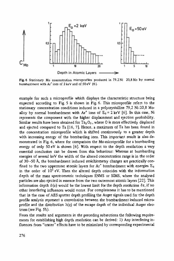
Fig. 6 Stationary Mo concentration microprofiles produced in 79,2Ni 20,8 Mo by normal bombardment with Ar § ions of 2 keV and of 50 eV [6].
example for such a microprofile which displays the characteristic structure being expected according to Fig. 5 is shown in Fig. 6. This microprofile refers to the stationary concentration conditions induced in a polycrystalline 79,2 Ni-20,8 Mo- alloy by normal bombardment with Ar § ions of Eo = 2 keV [6]. In this case, Ni represents the component with the higher displacement and ejection probability. Similar results have been obtained for Ta20s, where O is more effectively displaced and ejected compared to Ta [16, 7]. Hence, a maximum of Ta has been found in the concentration microprofile which is shifted continuously to a greater depth with increasing energy of the bombarding ions. This important result is also de- monstrated in Fig. 6, where for comparison the Mo-microproffle for a bombarding energy of only 50 eV is shown [6]. With respect to the depth resolution a very essential conclusion can be drawn from this behaviour: Whereas at bombarding energies of several keV the width of the altered concentration range is in the order of 30--50 A, the bombardment induced stoichiometry changes are practically con- fined to the two uppermost atomic layers for Ar § bombardment with energies Eo in the order of 102 eV. Then the altered depth coincides with the information depth of the mass spectrometric techniques SNMS or SIMS, where the analysed particles are also ejected in essence from the two outermost atomic layers [22]. This information depth ~ (z) would be the lowest limit for the depth resolution /Sz, if no other interfering influences would occur. For completeness it has to be mentioned that in the case of AES sputter depth profiling the Auger signals used for the depth profile analysis represent a convolution between the bombardment induced micro- profile and the distribution X(z) of the escape depth of the individual Auger elec- trons (see Fig. 5b).
From the results and arguments in the preceding subsections the following require- ments for establishing high depth resolution can be derived: 1) Any interfering in- fluences from "crater" effects have to be minimized by corresponding experimental
276
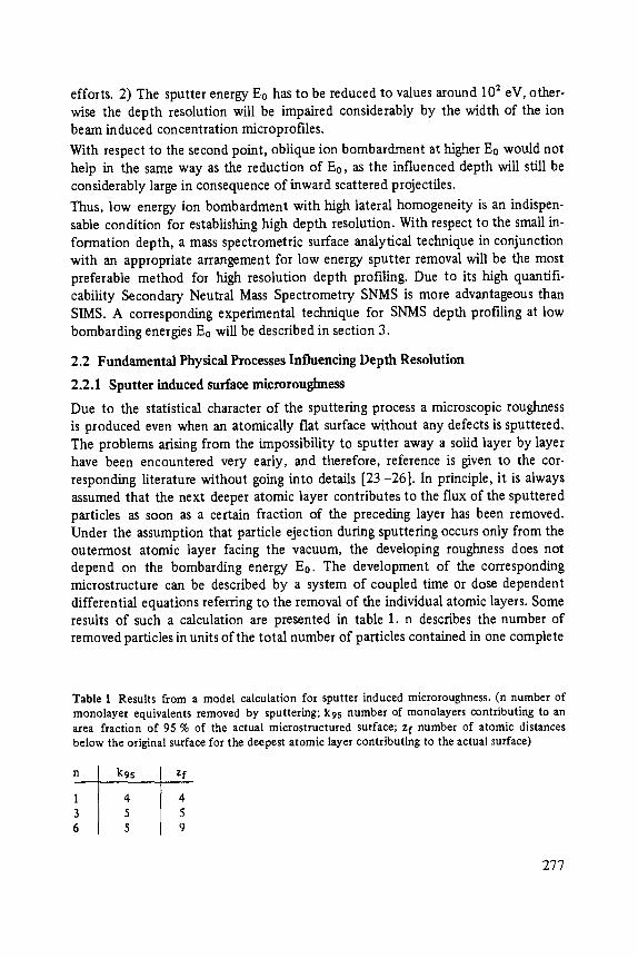
efforts. 2) The sputter energy Eo has to be reduced to values around 102 eV, other- wise the depth resolution will be impaired considerably by the width of the ion beam induced concentration microprofiles.
With respect to the second point, oblique ion bombardment at higher Eo would not help in the same way as the reduction of Eo, as the influenced depth will still be considerably large in consequence of inward scattered projectiles.
Thus, low energy ion bombardment with high lateral homogeneity is an indispen- sable condition for establishing high depth resolution. With respect to the small in- formation depth, a mass spectrometric surface analytical technique in conjunction with an appropriate arrangement for low energy sputter removal will be the most preferable method for high resolution depth profiling. Due to its high quantifi- cability Secondary Neutral Mass Spectrometry SNMS is more advantageous than SIMS. A corresponding experimental technique for SNMS depth profiling at low bombarding energies E0 will be described in section 3.
2.2 Fundamental Physical Processes Influencing Depth Resolution
2.2.1 Sputter induced surface microrouglmess
Due to the statistical character of the sputtering process a microscopic roughness is produced even when an atomically flat surface without any defects is sputtered. The problems arising from the impossibility to sputter away a solid layer by layer have been encountered very early, and therefore, reference is given to the cor- responding literature without going into details [23-26]. In principle, it is always assumed that the next deeper atomic layer contributes to the flux of the sputtered particles as soon as a certain fraction of the preceding layer has been removed. Under the assumption that particle ejection during sputtering occurs only from the outermost atomic layer facing the vacuum, the developing roughness does not depend on the bombarding energy Eo. The development of the corresponding microstructure can be described by a system of coupled time or dose dependent differential equations referring to the removal of the individual atomic layers. Some results of such a calculation are presented in table 1. n describes the number of removed particles in units of the total number of particles contained in one complete
Table 1 Results from a model calculation for sputter induced microroughness. (n number of monolayer equivalents removed by sputtering; kgs number of monolayers contributing to an area fraction of 95 % of the actual mierostructured surface; zf number of atomic distances below the original surface for the deepest atomic layer contributing to the actual surface)
n k95 zf
1 4 4 3 5 5 6 5 9
277
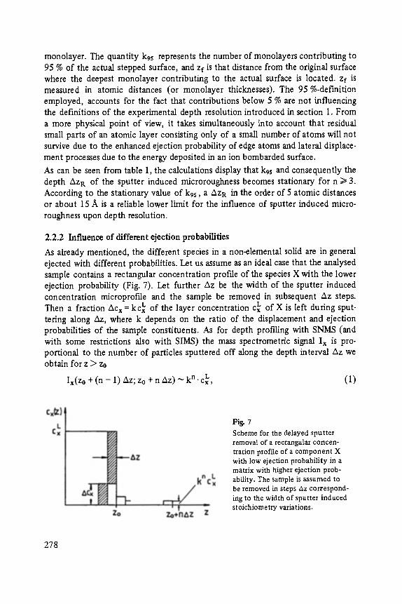
monolayer. The quantity kgs represents the number of monolayers contributing to 95 % of the actual stepped surface, and zf is that distance from the original surface where the deepest monolayer contributing to the actual surface is located, zf is measured in atomic distances (or monolayer thicknesses). The 95 %-definition employed, accounts for the fact that contributions below 5 % are not influencing the definitions of the experimental depth resolution introduced in section 1. From a more physical point of view, it takes simultaneously into account that residual small parts of an atomic layer consisting only of a small number of atoms will not survive due to the enhanced ejection probability of edge atoms and lateral displace- ment processes due to the energy deposited in an ion bombarded surface.
As can be seen from table 1, the calculations display that kgs and consequently the depth AZR of the sputter induced microroughness becomes stationary for n/> 3. According to the stationary value of kgs, a AzR in the order of 5 atomic distances or about 15 A is a reliable lower limit for the influence of sputter induced micro- roughness upon depth resolution.
2.2.2 Influence of different ejection probabilities
As already mentioned, the different species in a non-elemental solid are in general ejected with different probabilities. Let us assume as an ideal case that the analysed sample contains a rectangular concentration profile of the species X with the lower ejection probability (Fig. 7). Let further Az be the width of the sputter induced concentration microproffle and the sample be removed in subsequent Az steps. Then a fraction ACx = kcx L of the layer concentration Cx L of X is left during sput- tering along Az, where k depends on the ratio of the displacement and ejection probabilities of the sample constituents. As for depth profiling with SNMS (and with some restrictions also with SIMS) the mass spectrometric signal Ix is pro- portional to the number of particles sputtered off along the depth interval Az we obtain for z > zo
Ix(z0 + (n - 1) Az; z0 + n Az) ~ k n. Cx L, (1)
Fig. 7 Scheme for the delayed sputter removal of a rectangular concen- tration proftle of a component X with low ejection probability in a matrix with higher ejection prob- ability. The sample is assumed to be removed in steps ~z correspond- ing to the width of sputter induced stoichiometry variations.
278
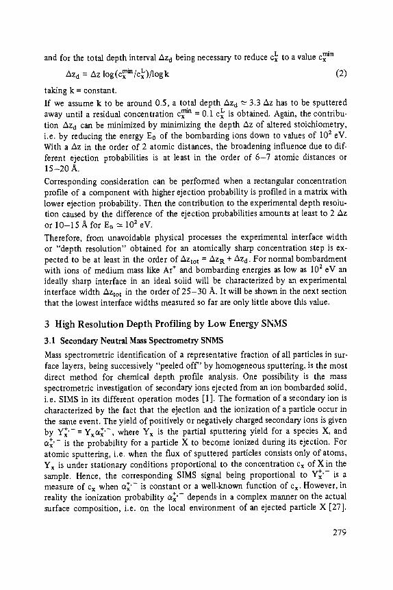
and for the total depth interval AZd being necessary to reduce Cx L to a value Cx rain
AZd = Az log (cxmin/cL)/1ogk (2)
taking k = constant.
If we assume k to be around 0.5, a total depth AZd ~- 3.3 Az has to be sputtered away until a residual concentration cx rain = 0.1 c L is obtained. Again, the contribu- tion Aza can be minimized by minimizing the depth Az of altered stoichiometry, i.e. by reducing the energy Eo of the bombarding ions down to values of 102 eV. With a Az in the order of 2 atomic distances, the broadening influence due to dif- ferent ejection probabilities is at least in the order of 6 -7 atomic distances or 15-20 A.
Corresponding consideration can be performed when a rectangular concentration profile of a component with higher ejection probability is profiled in a matrix with lower ejection probability. Then the contribution to the experimental depth resolu- tion caused by the difference of the ejection probabilities amounts at least to 2 Az or 10-15 Afor Eo "" 102 eV.
Therefore, from unavoidable physical processes the experimental interface width or "depth resolution" obtained for an atomically sharp concentration step is ex- pected to be at least in the order of AZto t = AZ R -t- AZ d. For normal bombardment with ions of medium mass like Ar+ and bombarding energies as low as 102 eV an ideally sharp interface in an ideal solid will be characterized by an experimental interface width AZto t in the order of 25--30 A. It will be shown in the next section that the lowest interface widths measured so far are only little above this value.
3 High Reso lu t ion Dep th Profil ing by Low Energy SNMS
3.1 Secondary Neutral Mass Spectrometry SNMS
Mass spectrometric identification of a representative fraction of all particles in sur- face layers, being successively "peeled off" by homogeneous sputtering, is the most direct method for chemical depth profde analysis. One possibility is the mass spectrometric investigation of secondary ions ejected from an ion bombarded solid, i.e. SIMS in its different operation modes [1]. The formation of a secondary ion is characterized by the fact that the ejection and the ionization of a particle occur in the same event. The yield of positively or negatively charged secondary ions is given by Y~'- = Yxax , where Yx is the partial sputtering yield for a species X, and a~'- is the probability for a particle X to become ionized during its ejection. For atomic sputtering, i.e. when the flux of sputtered particles consists only of atoms, Yx is under stationary conditions proportional to the concentration Cx of X in the sample. Hence, the corresponding SIMS signal being proportional to Y~'- is a measure of Cx when ax is constant or a well-known function of Cx. However, in reality the ionization probability c~,~'- depends in a complex manner on the actual surface composition, i.e. on the local environment of an ejected particle X [27].
279

§ m ax can be correlated to the actual surface concentrations only in a few cases [28]. Moreover, as described in section 2.2.2 the surface composition itself is in general a complicated function of the original sample composition which is the goal of the analysis.
An example for a strong non-linear variation of the SIMS signal with the surface composition is shown in Fig. 8. The signal of the atomic Ta§ decreases rapidly, when the oxygen is continuously removed from an originally oxidized Ta-surface by ion bombardment, as demonstrated by the simultaneously measured AES-signal for oxygen [29]. (See also Ref. [30].) Such a behaviour demonstrates clearly the difficulties to get reliable depth profiles for oxide interfaces with SIMS.
Due to the coupling of the ejection and the ionization process it is impossible in many cases to distinguish between the influences described by Yx and a ~ ' - and to correlate the SIMS signals from an unknown sample to its composition. As an ex-
- l - j - ception from this complicated situation, a x can be taken as a constant for low concentrations of a species X. Then the ejection of X occurs always under identical
Fig. 8 SIMS and SNMS signals of positively charged and neutral Ta atoms during the sputter removal of a thin Ta oxide overlayer (~ 2 monolayers) on polycrystalline Ta by 4 keV Ar § ions under 45 ~ For comparison the variation of the simultaneously measured 510 eV-O-peak from AES is included [29].
280
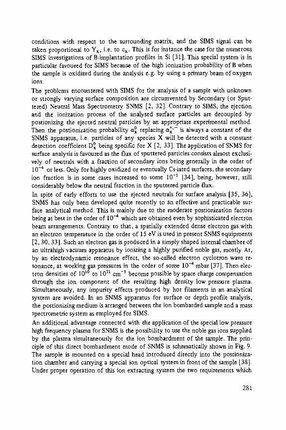
conditions with respect to the surrounding matrix, and the SIMS signal can be taken proportional to Yx, i.e. to Cx. This is for instance the case for the numerous SIMS investigations of B-implantation profiles in Si [31]. This special system is in particular favoured for SIMS because of the high ionization probability of B when the sample is oxidized during the analysis e.g. by using a primary beam of oxygen ions.
The problems encountered with SIMS for the analysis of a sample with unknown or strongly varying surface composition are circumvented by Secondary (or Sput- tered) Neutral Mass Spectrometry SNMS [2, 32]. Contrary to SIMS, the ejection and the ionization process of the analysed surface particles are decoupled by postionizing the ejected neutral particles by an appropriate experimental method.
0 -1%- T h e n the postionization probability ax replacing a x is always a constant of the SNMS apparatus, i.e. particles of any species X will be detected with a constant detection coefficient D O being specific for X [2, 33]. The application of SNMS for surface analysis is favoured as the flux of sputtered particles consists almost exclusi- vely of neutrals with a fraction of secondary ions being generally in the order of 10 -4 or less. Only for highly oxidized or eventually Cs-iated surfaces, the secondary ion fraction is in some cases increased to some 10 -x [34], being, however, still considerably below the neutral fraction in the sputtered particle flux. In spite of early efforts to use the ejected neutrals for surface analysis [35, 36], SNMS has only been developed quite recently to an effective and practicable sur- face analytical method. This is mainly due to the moderate postionization factors being at best in the order of 10 -4 which are obtained even by sophisticated electron beam arrangements. Contrary to that, a spatially extended dense electron gas with an electron temperature in the order of 15 eV is used in present SNMS equipments [2, 30, 33]. Such an electron gas is produced in a simply shaped internal chamber of an ultrahigh vacuum apparatus by ionizing a highly purified noble gas, mostly Ar, by an electrodynamic resonance effect, the so-called electron cyclotron wave re- sonance, at working gas pressures in the order of some 10-* mbar [37]. Then elec- tron densities of 101~ to 1011 cm -3 become possible by space charge compensation through the ion component of the resulting high density low pressure plasma. Simultaneously, any impurity effects produced by hot filaments in an analytical system are avoided. In an SNMS apparatus for surface or depth profile analysis, the postionizing medium is arranged between the ion bombarded sample and a mass spectrometric system as employed for SIMS.
An additional advantage connected with the application of the special low pressure high frequency plasma for SNMS is the possibility to use the noble gas ions supplied by the plasma simultaneously for the ion bombardment of the sample. The prin- ciple of this direct bombardment mode of SNMS is schematically shown in Fig. 9. The sample is mounted on a special head introduced directly into the postioniza- tion chamber and carrying a special ion optical system in front of the sample [38]. Under proper operation of this ion extracting system the two requirements which
281
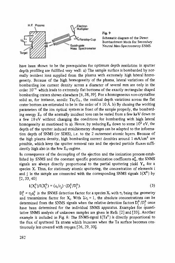
Fig. 9 Schematic diagram of the Direct Bombardment Mode for Secondary Neutral Mass Spectrometry SNMS.
have been shown to be the prerequisites for optimum depth resolution in sputter depth profiling are fulfilled very well: a) The sample surface is bombarded by nor- mally incident ions supplied from the plasma with extremely high lateral homo- geneity. Because of the high homogeneity of the plasma, lateral variations of the bombarding ion current density across a diameter of several mm are only in the order 10 -s which leads to extremely fiat bottoms of the exactly rectangular shaped bombarding craters shown elsewhere [6, 38, 39]. For a homogeneous non-crystalline solid as, for instance, anodic Ta2Os, the residual depth variations across the fiat crater bottom are estimated to be in the order of + - 10 A. b) By chosing the working parameters of the ion optical system in front of the sample properly, the bombard- ing energy Eo of the normally incident ions can be varied from a few keV down to a few 10 eV without changing the conditions for bombarding with high lateral homogeneity as mentioned in a). Hence, by reducing Eo down to some 102 eV, the depth of the sputter induced stoichiometry changes can be adapted to the informa- tion depth of SNMS (or SIMS), i.e. to the 2 outermost atomic layers. Because of the high plasma density, high bombarding current densities around 1 mA/cm 2 are possible, which keep the sputter removal rate and the ejected particle fluxes suffi- ciently high also in the low Eo-regime. In consequence of the decoupling of the ejection and the ionization process estab- lished by SNMS and the constant specific postionization coefficents a~ the SNMS signals are always directly proportional to the partial sputtering yield Yx for a species X. Thus, for stationary atomic sputtering, the concentration of elements i and j in the sample are connected with the corresponding SNMS signals I(X ~ by [2, 33, 40]
I(X ~ )/t(xj ' ) : (ci/c j) -(O ~ ~ (3)
D O = r/i a~ is the SNMS detection factor for a species X i with rli being the geometry and transmission factor for Xi. With Eci = 1, the absolute concentrations can be determined from the SNMS signals when the relative detection factors D o/D ~ once have been determined for the individual SNMS apparatus. Examples for quanti- tative SNMS analysis of unknown samples are given in Refs. [2] and [33]. Another example is included in Fig. 8: The SNMS-signal I(Ta ~ is directly proportional to the flux of sputtered Ta atoms which increases when the Ta surface becomes con- tinuously less covered with oxygen [26, 29, 30].
282
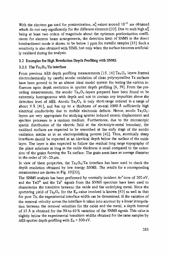
With the electron gas used for postionization, a~ around 10 -2 are obtained which do not vary significantly for the different elements [33]. Due to such high a~ being at least two orders of magnitude about the optimum postionization coeffi- cients for electron beam arrangements, the detection limit of SNMS in the direct bombardment mode is shown to be below 1 ppm for metallic samples [33]. Such a sensitivity is also obtained with SIMS, but only when the surface becomes artificial- ly oxidized during the analysis.
3.2 Examples for High Resolution Depth Prof'ding with SNMS
3.2.1 The Ta2Os/Ta interface
From previous AES depth profiling measurements [15, 16] Ta2Os layers formed electrochemically by careful anodic oxidation of clean polycrystalline Ta surfaces have been proved to be an almost ideal model system for testing the various in- fluences upon depth resolution in sputter depth profiling [6, 39]. From the pre- ceding measurements, the anodic Ta2Os-layers prepared have been found to be extremely homogeneous with depth and not to contain any impurities above the detection level of AES. Anodic Ta2Os is only short-range ordered in a range of about 9 A [41], and has up to a thickness of several 1000 A sufficiently high electrical conductivity due to mobile electronic defects. Hence, anodic Ta2Os- layers are very appropriate for studying sputter induced atomic displacement and ejection processes in a random medium. Furthermore, due to the microscopic spatial distribution of the electric field at the electrolyte-metal boundary, the oxidized surfaces are expected to be smoothed at the early stage of the anodic oxidation similar as in an electropolishing process [42]. Thus, atomically sharp interfaces should be expected at an identical depth below the surface of the oxide layer. The layer is also expected to follow the residual long range topography of the plane substrate as long as the oxide thickness is small compared to the exten- sion of the gains forming the Ta surface. The grain areas have an average diameter in the order of 10-20/am.
In view of these properties, the Ta2Os/Ta interface has been used to check the depth resolution obtained by low energy SNMS. The results for a corresponding measurement are shown in Fig. 10 [33].
The SNMS analysis has been performed by normally incident Ar+-ions of 202 eV, and the TaO ~ and the Ta ~ signals from the SNMS spectrum have been used to characterize the transition between the oxide and the underlying metal. Since the sputtering yield of Ta2Os for the Eo-value involved is known [43] as well as that for pure Ta, the experimental interface width can be determined. If the variation of the removal velocity across the interface is taken into account by a linear interpola- tion between the removal velocities for the oxide and the metal, a depth interval of 33 )k is obtained for the 90-to-10 % variation of the SNMS signals. This value is slightly below the experimental transition widths obtained for the same samples by AES sputter depth profiling with Eo = 500 eV.
283
Fig. 10 Low energy SNMS depth profiling of the interface between an anodic Ta20 s layer on polycrystalline Ta by normally incident At" ions of 202 eV [33 ].
According to the considerations in section 2.2 a minimum experimental interface width of approx. 25-30 A is expected for profiling an atomically sharp concentra- tion step due to sputter induced microroughness and different ejection probabilities. If the experimental interface width from Fig. 10 is corrected accordingly, a residual value of a few A is left which corresponds to the optimum absolute depth resolu- tion 6z for depth profiling with low bombarding energies. Hence, it has to be con- cluded that the variations of the SNMS signals in Fig. 10 describe the residual effects obtained for an atomically sharp oxide-metal-interface. Vise-versa, an atomi- cally sharp interface can be identified by such a measurement.
Similar results have been obtained by Kirschner and Etzkorn [44] with AES sputter depth profiling of a carefully prepared Ge/Si-interface for the bombardment with Xe § ions under 50 ~ against the normal onto the sample surface. For Eo = 500 eV an experimental width of 25 ,~ has been measured for the 84-to-16 %-transition of the corresponding AES signals, being corrected for the escape depth of the Auger elec- trons. If the 90-to-10 %-definition used in Fig. 10 is applied to results for the Ge/Si- interface, the corresponding transition width amounts to 36 A which is very close to the SNMS results for the Ta20s-Ta interface.
When SNMS profiling is performed under such experimental conditions which have been found to yield a minimum experimental transition width for profiling a sharp
284

concentration step, an unknown concentration profile is determined also with optimum depth resolution. If the depth profiled component X again has a different ejection probability compared to the surrounding matrix, similar arguments as those in connection with Fig. 7 can be applied to establish a relation between the SNMS signal I (X ~ ; z) for the species X and the true concentration of X in a depth z. We obtain [2]
I (X~ ~ Cx(Z ) -+ k Az(SCx/~Z)z
Cx(Z) (4)
where the correction term 6c x depends on the slope of the concentration profile at the depth z, and on the width Az of altered sample stoichiometry. Again the specimen is assumed to be sputtered off in steps Az. As in the context with Fig. 7, the factor k describes the ratio of the different ejection probabilities of X and the surrounding matrix.
If c x is assumed to vary by 1 order of magnitude along a depth interval of 20 atomic distances, and k again is taken as 0.5, the relative error of c x due to the correction term 6Cx is found to be ~Cx/Cx ~- 5 - 10 -z for Az ~- 2 atomic distances, i.e. for a removal energy around Eo = 102 eV. This error, however, increases already to 6Cx/Cx "" 0.25, when Az is increased to a value of about 10 atomic distances, i.e. for a bombarding energy Eo in the order of 1 keV. Hence, the signal obtained by depth profiling with low energy SNMS is proportional to the true Cx-Values with an accuracy of several percent, even for the assumed steep slope of a concentration profile. In order to demonstrate the high depth resolution obtained with low energy SNMS, an analysis of a shallow, highly structured phosphorous profile in silicon is shown in Fig. 11 [45]. The sample has been prepared by implanting an unusually high P-dose of 5" 10 6 P atoms/cm 2 at an implantation energy of 60 keV. Sputter depth profiling was performed with normally incident Ar§ of 290 eV. During the depth pro- filing measurement the mass 31-peak in the SNMS spectrum was continuously re- corded. A major contribution from 3~ can be excluded as the Si-peaks represent well the corresponding natural isotope ratios. The characteristic structure of the profile has been reproduced by a number of measurements for different samples from the same implantation wafer. The sputter time axis is being converted into a depth scale by means of the bombarding current density of 2,72 mA/cm 2 and the total sputtering yield for Si under normal bombardment of 290 eV Ar+-ions as taken from the literature (0.33 Si-atoms/ion) [46]. The concentration axis was calibrated according to the procedure described in section 3.1.
The purpose of Fig. 11 is to demonstrate the possibilities of low energy SNMS for high resolution sputter depth profiling rather than to discuss the profile structure of the specially prepared sample. Even for the steepest slope in the P-profile in Fig. 11, the relative contribution ~Cp/Cp of the correction term according to Eq. 4 is in
285
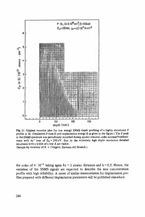
Fig. 11 Original recorder plot for low energy SNMS depth profiling of a highly structured P profile in SL (Implanted P dose D and implantation energy E as given in the figure.) The P peak in the SNMS spectrum was periodieaUy recorded during sputter removal under normal bombard- ment with Ar § ions of Eo = 290 eV. Due to the extremely high depth resolution detailed structures with a width of a few A are visible. (Sample by courtesy of R. v. Criegern, Siemens AG Munich.)
the order o f 4 . 1 0 -2 taking again 6z ~- 2 a tomic distances and k = 0,5. Hence , the
variation o f the SNMS signals are expected to describe the true concen t r a t ion
profi le with high reliability. A series of similar measurements for implan ta t ion pro-
files prepared with different implanta t ion parameters will be published elsewhere.
286
4 Conc lus ions
From the arguments and discussions presented in section 2 we have to conclude that apart from the minimization of interfering effects from the bombarding crater, the energy of the bombarding ions used for the sputter removal of the sample has to be reduced down to energies Eo around 102 eV. Then, interfering variations of the sample stoichiometry wiU be reduced in a good approximation to the 2 outer- most atomic layers of the sample. Such a minimum depth coincides with the infor- mation depth of mass spectrometric methods for surface analysis, namely SNMS and SIMS. This information depth has to be considered as the optimum absolute depth resolution 6z in depth profile analysis.
In addition to such influences which can be minimized experimentally, the effects from unavoidable physical processes connected with the sputtering process itself have to be taken into account. These influences produce an atomic microroughness of a depth of approx. 5 atomic distances due to the statistical character of sput- tering, and a delayed or preferred removal of a component due to different specific ejection probabilities. The latter influence may impair the depth resolution also at least by 4 - 6 atomic distances.
Hence, a total experimental transition width of about 25-30 A is expected to be induced by such influences when an atomically sharp interface in an ideal matrix is depth profded. A transition width of such an order, which may be obtained when other interfering effects have been eliminated experimentally, is therefore represen- tative for an atomically sharp concentration step at a solid interface.
It has been shown that the direct bombardment mode of Secondary Neutral Mass Spectrometry SNMS is very appropriate for high resolution depth profiling because of the quantitative correlation between the SNMS signals and the concentration values, and, equally important, because of the possibility to use extremely low bombarding energies for depth profiling. With this method, experimental transition widths for atomically sharp interfaces have been obtained which correspond to the interface broadening expected from the natural limitations involved in sputter depth profiling.
References [ 1] A. Benninghoven, F. RiMenauer, and H. W. Werner, Secondary Ion Mass Spectrometry (J.
Wiley & Sons, New York, 1984). [2] H. Oechsner in: Thin Film and Depth Profile Analysis, ed. by H. Oechsner, Topics in
Current Physics Vol. 37, Heidelberg, Berlin, New York, Springer-Verlag 1984. [3] J. E. Greene, F. Sequeda.Osorio, B. R. Natarajan: J. Appl. Phys. 46, 2701 (1975). [4] S. Hofmann in: Thin Film and Depth Profile Analysis, ed. by H. Oechsner, Topics in
Current Physics Vol. 37, Heidelberg, Berlin, New York, Springer-Verlag 1984. [5] Handbook of X-ray and Ultraviolet Photoelectron Spectroscopy. Ed. D. Briggs, London,
Philadelphia, Rheine, Heyden, 1977.
287
[61 J. Bartella and 1t. Oechsner, Surf. Sci. 126,581 (1983).
[71 H. Oechsner, Proc. IX Intern. Vac. Congress and V Int. Conf. Solid Surf., Madrid 1983, Invited Speakers' Vol. pp. 316.
[81 K. Wittmaack, Vacuum 34, 119 (1984).
[9] C. Ir Magee, W. L. Harrington, and R. E. Honig, Rev. Sci. Instrum. 49,477 (1978).
[10] R.v. Crieger, L lCeitzel, and Z Fottner in: Secondary Ion Mass Spectrometry SIMS IV, ed. by A. Benninghoven, J. Okano, R. Shimizu and H. W. Werner, Springer Ser. Chem. Phys. Vol. 36, Berlin, Heidelberg, New York, Tokyo, Springer-Verlag 1984, p. 308.
[111 K. R61l and Ch. Hammer, Thin Solid Films 57,209 (1979).
[121 S. Hofmann and A. Zalar, Thin Solid Films 60, 201 (1979).
113] H.W. Werner, Surf. Interf. Anal. 4, 1 (1982).
[ 14] Z Giber, 1). Marton, J. Laszlo, A. Hanusovszky, and P. Stingeder, Vacuum 33, 117 (1983)
[15] H. Schoof and H. Oechsner, Proc. 4th Int. Conf. Sol. Surf. and 3d ECOSS (Ed. by D. A. Degras and M. Costa), LeVide, les Couches Minces (Suppl.) 201, 1291 (1980).
[16]. H. School Thesis, Techn. Univ. Clausthal 1981.
[ 171 J.M. Sanz Martinez, Thesis, Univ. Stuttgart 1982.
[18] P. Sigmund, Phys. Rev. 184, 383 (1969); cf. also 187,768 (1969).
[191 U. Littmark and Ir Hofer in: Thin Film and Depth Profile Analysis, ed. by H. Oechsner, Topics in Current Physics Vol. 37, Heidelberg, Berlin, New York, Springer-Verlag 1984.
[20] H. W. Etzkorn, Z ICahrhusen, and H. Oechsner, Fresenius Z. Anal. Chem. 314, 265 (1983) and to be published.
[21] G. Betz, Surface Sci. 92,283 (1980).
1221 H. Eckstein and Z Biersack, Appl. Phys. 33 (1984), in print.
[23] A. Benninghoven, Z. Physik 230, 403 (1970).
1241 S. Hofmann, Appl. Phys. 9, 59 (1976).
[25] Z Erlewein and S. Hofmann, Thin Solid Films 69, L39 (1980).
[26] 1-1. Oechsner and A. ICucher, Appl. Surf. Sci. 10, 342 (1982).
1271 Z. Sroubek, Nucl. Instr. Meth. 194, 533 (1982).
[281 H. Oechsner and Z. Sroubek, Surf. Sci. 127, 10 (1983).
[29] H. Oechsner and E. Stumpe, Proc. 4th Int. Conf. Sol. Surf. and 3d ECOSS (Ed. by D. A. Degras and M. Costa), LeVide, Les Couches Minces (Suppl.) 201, 1234 (1980).
[30] H. Oechsner, W. RiJhe, and E. Stumpe, Surf. Sci. 85,289 (1979).
1311 K. ICittmaack, Radiation Effects, 63,205 (1982).
[321 H. Oechsner, Appl. Phys. 8, 185 (1975).
[33] K.H. Mailer and H. Oechsner, Microchimica Acta, Suppl. 10, 51 (1983), (Progress in Materials Analysis, Vol. 1, ed. by M. Grasserbauer and M. K. Zacherl, Springer, Wien, New York, 1983).
[341 H. A. Storms, K. L Brown, and J. D. Stein, Analytical Chem. 49, 2023 (1977).
1351 R.E. Honig, J. Appl. Phys. 29,549 (1958).
{361 J. R. Woodyard, C. B. Cooper, J. Appl. Phys. 35,1107 (1964).
[371 H. Oechsner, Plasma Physics 16,835 (1974).
I381 E. Stumpe, H. Oechsner, and I-1. Schoofi Appl. Phys. 20, 55 (1979).
[391 H. Oechsner, Fresenius Z. Anal. Chem. 314,211 (1983).
288

[40] H. Oechsner in: Secondary Ion Mass Spectrometry SIMS IV, ed. by A. Benninghoven, J. Okano, R. Shimizu and H. W. Werner, Springer Set. Chem. Phys. Vol. 36, Berlin, Heidelberg, New York, Tokyo, Springer-Verlag 1984, p. 291.
[41] P. Schulze and K. Heusler, Ber. Bunsenges. 78, 601 (1974). [421 J. Whitton, priv. communication. [43] H. Oechsner, H. School, and E. Stumpe, Surf. Sci. 76,343 (1978).
[441 s Kirschner and H. W. Etzkorn in: Thin Film and Depth Profile Analysis, ed. by H. Oechsner, Topics in Current Physics Vol. 37, Heidelberg, Berlin, New York, Springer- Verlag 1984.
[451 H. Paulus, Diploma thesis, Univ. Kaiserslautern 1984.
[46] H. El. Andersen and H. L. Bay in: Sputtering by Particle Bombardment I ed. by R. Behrisch, Topics in Applied Physics Vol. 47, Berlin, Heidelberg, New York, Springer-Vet- lag 1981, pp. 145.
289
Festk6rperprobleme XX lV (1984)
Inelastic Light Scattering in Semiconductor Heterostructures
Gerhard Abstreiter
Physik-Department E 16, Technische Llniversit~it MiJnchen, Garching, Federal Republic of Germany
Summary: Resonant inelastic light scattering is used as a versatile tool for the investigation of semiconductor surfaces and interfaces. Phonon scattering spectra yield direct information on structure, surface orientation, and composition of semiconductor layers as thin as a few mono- layers. "Forbidden" electric-field induced LO-phonon scattering in polar semiconductors leads to information on surface or interface barrier heights. The formation of semiconductor hetero- structures is studied "in situ" for the GaAs/Ge system. Electronic Raman scattering is used widely to investigate subband energies and carrier concentrations in space charge layers at semi- conductor interfaces as well as in superlattices.
1 Introduction
Semiconductor heterostructures have received considerable attention for a long time, a fact which is caused primarily by their importance for electronic and electro- optic solid state devices. The development of crystal growth techniques like mole- cular beam epitaxy (MBE) and metal organic chemical vapor deposition (MOCVD) made it possible to grow heterostructures with abrupt interfaces. In this way semi- conductor superlattices, composed of ultrathin layers of different materials have been achieved and studied experimentally and theoretically [ 1-4] . The electronic and optical properties of these heterostructure-superlattices are determined by the properties of the interfaces, especially by the band-gap discontinuities and by the space charge fields. Depending on the sign of the band edge discontinuities between the two semiconductors involved one distinguishes between several types of hetero- junctions. In the present work I want to focus the attention only to systems for which the conduction and valence band discontinuities have opposite signs. Then the type of doping in both semiconductors determines the space charge fields normal to the heterojunction interface. In the case that both layers are n-type, electrons from the donors in the wide-gap material are transferred into the ener- getically lower conduction band of the semiconductor with smaller band gap, forming an accumulation layer at the interface. This is shown schematically in Fig. la. Here it is assumed that the valence band discontinuity is equal to the con- duction band discontinuity and that the band gap E~ on the one side of the hetero- junction is approximately twice El , the energy gap of the second semiconductor.
291
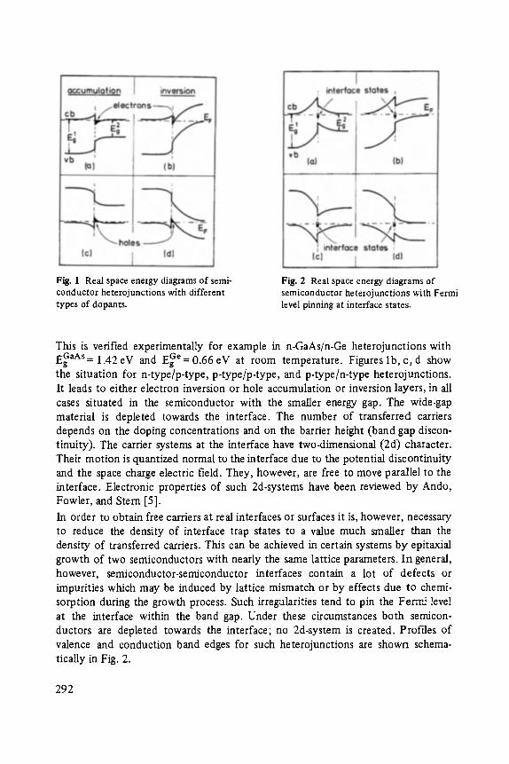
Fig. 1 Real space energy diagrams of semi- conductor heterojunctions with different types of dopants.
Fig. 2 Real space energy diagrams of semiconductor heterojunctions with Fermi level pinning at interface states.
This is verified experimentally for example in n-GaAs/n-Ge heterojunctions with Eg GaAs= 1.42 eV and E Ge= 0.66 eV at room temperature. Figures lb, c, d show the situation for n-type/p-type, p-type/p-type, and p-type/n-type heterojunctions. It leads to either electron inversion or hole accumulation or inversion layers, in all cases situated in the semiconductor with the smaller energy gap. The wide-gap material is depleted towards the interface. The number of transferred carriers depends on the doping concentrations and on the barrier height (band gap discon- tinuity). The carrier systems at the interface have two-dimensional (2d) character. Their motion is quantized normal to the interface due to the potential discontinuity and the space charge electric field. They, however, are free to move parallel to the interface. Electronic properties of such 2d-systems have been reviewed by Ando, Fowler, and Stem [5].
In order to obtain free carriers at real interfaces or surfaces it is, however, necessary to reduce the density of interface trap states to a value much smaller than the density of transferred carriers. This can be achieved in certain systems by epitaxial growth of two semiconductors with nearly the same lattice parameters. In general, however, semiconductor-semiconductor interfaces contain a lot of defects or impurities which may be induced by lattice mismatch or by effects due to chemi- sorption during the growth process. Such irregularities tend to pin the Fermi level at the interface within the band gap. Under these circumstances both semicon- ductors are depleted towards the interface; no 2d-system is created. Profiles of valence and conduction band edges for such heterojunctions are shown schema- tically in Fig. 2.
292
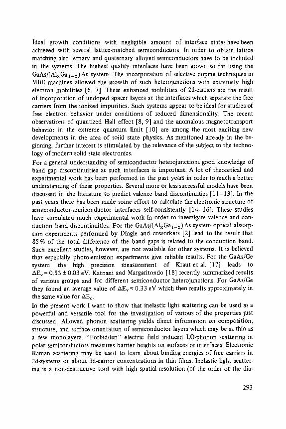
Ideal growth conditions with negligible amount of interface states have been achieved with several lattice-matched semiconductors. In order to obtain lattice matching also ternary and quaternary alloyed semiconductors have to be included in the systems. The highest quality interfaces have been grown so far using the GaAs/(AlxGal_x) As system. The incorporation of selective doping techniques in MBE machines allowed the growth of such heterojunctions with extremely high electron mobilities [6, 7]. These enhanced mobilities of 2d-carriers are the result of incorporation of undoped spacer layers at the interfaces which separate the free carriers from the ionized impurities. Such systems appear to be ideal for studies of free electron behavior under conditions of reduced dimensionality. The recent observations of quantized Hall effect [8, 9] and the anomalous magnetotransport behavior in the extreme quantum limit [10] are among the most exciting new developments in the area of solid state physics. As mentioned already in the be- ginning, further interest is stimulated by the relevance of the subject to the techno- logy of modern solid state electronics.
For a general understanding of semiconductor heterojunctions good knowledge of band gap discontinuities at such interfaces is important. A lot of theoretical and experimental work has been performed in the past years in order to reach a better understanding of these properties. Several more or less successful models have been discussed in the literature to predict valence band discontinuities [ 11-13]. In the past years there has been made some effort to calculate the electronic structure of semiconductor-semiconductor interfaces self-consistently [ 14-16]. These studies have stimulated much experimental work in order to investigate valence and con- duction band discontinuities. For the GaAs/(AlxGal_x)As system optical absorp- tion experiments performed by Dingle and coworkers [2] lead to the result that 85 % of the total difference of the band gaps is related to the conduction band. Such excellent studies, however, are not available for other systems. It is believed that especially photo-emission experiments give reliable results. For the GaAs/Ge system the high precision measurement of Kraut et al. [17] leads to AEv = 0.53 -+ 0.03 eV. Katnani and Margaritondo [18] recently summarized results of various groups and for different semiconductor heterojunctions. For GaAs/Ge they found an average value of AEv = 0.33 eV which then results approximately in the same value for AEc. In the present work I want to show that inelastic light scattering can be used as a powerful and versatile tool for the investigation of various of the properties just discussed. Allowed phonon scattering yields direct information on composition, structure, and surface orientation of semiconductor layers which may be as thin as a few monolayers. "Forbidden" electric field induced LO-phonon scattering in polar semiconductors measures barrier heights on surfaces or interfaces. Electronic Raman scattering may be used to learn about binding energies of free carriers in 2d-systems or about 3d-carrier concentrations in thin films. Inelastic light scatter- hag is a non-destructive tool with high spatial resolution (of the order of the dia-
293
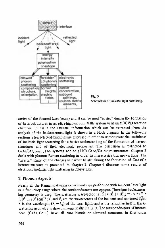
Fig. 3 Schematics of inelastic light scattering.
meter of the focused laser beam) and it can be used "ha situ" during the formation of heterostructures in an ultra-high-vacuum MBE system or ha an MOCVD reaction chamber. In Fig. 3 the essential information which can be extracted from the analysis of the backscattered light is shown in a block diagram. In the following sections a few selected examples are discussed in order to demonstrate the usefulness of inelastic light scattering for a better understanding of the formation o f hetero- structures and of their electronic properties. The discussion is restricted to GaAs/(AlxGal_x)As systems and to (110) GaAs/Ge heterostructures. Chapter 2 deals with phonon Raman scattering in order to characterize thin grown films. The "in situ" study of the changes in barrier height during the formation of GaAs/Ge heterostructures is presented ha chapter 3. Chapter 4 discusses some results of electronic inelastic light scattering in 2d-systems.
2 P h o n o n Aspec t s
Nearly all the Raman scattering experiments are performed with incident laser light in a frequency range where the semiconductors are opaque. Therefore backscatter-
�9 ~ - ' )" ~9" n
hag geometry is used�9 The scattering wavevector Is Iq [ = Ikil + Iksl ~ '2 x 21r7~ (10 s ... 106) cm -1 ; ~i and k~ are the wavevectors of the incident and scattered light, ~, is the wavelength (~-i ~" ~-s) of the laser light, and n the refractive index�9 Back- scattering geometry is shown schematically in Fig. 3. The semiconductors o f interest here (GaAs, Ge ...) have all zinc blende or diamond structure. In first order
294

"allowed" Raman scattering one measures the optical phonons close to the center of the Brillouin zone. In polar semiconductors like GaAs the phonons are split into the twofold degenerate TO-mode and the nondegenerate LO-mode. This is not the case in Si or Ge. From the selection rules one learns that not all components of the optical phonons are allowed under a given scattering configuration. Following Loudon's description of the Raman tensors [19] one Finds that for crystals with zinc blende structure in backscattering from (100) surfaces only the LO-phonons can be observed. From (110) cleavage surfaces on the other hand only TO-phonons are allowed. These selection rules have been used to get direct information on the orientation of thin epitaxial films of GaAs grown with MBE [20]. It has been demonstrated that carbon contamination of the starting surface leads to misorienta- tion of the growing films.
In mixed crystals like (AlxGal_x)AS, phonon Raman scattering can be used to obtain information on the composition. The optical phonons in these crystals have a two-mode behavior with frequencies close to the modes of pure GaAs or pure AlAs. The frequency dependence of these modes on the molar fraction x of AI in GaAs has been used to study depth profiles of the Al-content in (AlxGal_x)AS films and the composition of thin films and multilayer structures [20]. The sensi- tivity of these Raman studies can be increased by working under resonance con- ditions [21]. If the energy of the incident laser light is approximately equal to an optical energy gap of the semiconductor, the scattered intensity may increase by several orders of magnitude. Under such conditions it is possible to study phonons of semiconductor layers as thin as a few monolayers. The nicest examples for such experiments have been performed for thin Ge-films on GaAs [22]. The results are discussed in more detail in the following.
Brugger et al. [22] have investigated "in situ" the formation of GaAs/Ge hetero- structures. The samples were prepared by cleaving single-crystals of Te-doped GaAs bars in an UHV chamber with base pressure < 10 -1~ mbar. High-purity Ge was evaporated from an effusion cell on to the (110) cleavage surfaces of the sub- strate. The sample temperature was varied from 100 K to 675 K. The growth rate did not exceed 0.05 A/s. The nature of the grown Ge films was studied by analyz- ing Raman spectra obtained with h~ L = 2.41 eV, a laser line which is close to the El + A1 energy gap of Ge. Fig. 4 shows examples for films grown at T = 675 K. The measuring temperature was 300 K. At low Ge coverages only the TO-phonon mode of GaAs is observed. As expected from the selection rules, no LO-phonon mode is present. The Ge-optical phonon mode appears in the spectrum already at a thickness of only 6 monolayers. Its intensity is increasing strongly with film thick- ness, concomitant with a decrease of the TO-phonon line of GaAs due to absorption of light in the Ge film. It should be mentioned that the Ge-phonon line exhibits a small but easily measurable shift to lower energies for thin layers. The bulk phonon energy of 37.4 meV is approached for layer thicknesses of more than 40 A. The shifts reflect the lattice dynamics of a thin crystalline Ge slab which is termi-
295

Fig. 4 Phonon Raman spectra of thin GaAs-Ge heterostructures grown at Tg = 675 K (from Ref. [22]).
Fig. 5 Phonon Raman spectra of GaAs-Ge heterostructures grown at Tg = 100 K (from Ref. [22]).
hated on one side by the GaAs substrate and has a free surface to the vacuum side. A similar behavior of the Ge-optical phonon mode has been observed for all films grown with small evaporation rates for growth temperatures Tg/> 300 K. A careful analysis of the lineshapes and intensities of the phonon lines show, however, that room temperature grown films are polycrystalline. Overlayers of similar thickness grown at higher temperatures exhibit sharper, more symmetric and more intense phonon lines indicating a higher quality of the epitaxial films.
Films grown at Tg = 100 K on the other hand do not show any sharp phonon struc- ture. Their Raman spectra are typical for amorphous Ge. They consist of two broad lines, where the stronger one peaks around 34meV. An example is shown in Fig. 5. The top curve again shows the GaAs TO-phonon line when no Ge is at the surface. A 140 A thick Ge film results in a weak structure which is still dominated by the GaAs phonon mode (middle curve in Fig. 5). In the lower spectrum a scattering configuration has been chosen for which both first order TO- and LO-phonon Raman scattering in GaAs are forbidden. So the amorphous nature of the grown Ge film can be observed directly in the spectrum. In the following chapter the structure of the grown Ge-films is related to the interface barrier heights.
296
3 Surface and In t e r f ace Barrier Heights
In polar III-V semiconductors Raman scattering by LO-phonons is symmetry for- bidden in backscattering from (110)-surfaces. It has been shown, however, that under resonance conditions symmetry breaking mechanisms can cause strong "forbidden" LO-phonon scattering. Three such mechanisms have been discussed in the literature [23]:
- Intraband scattering of electrons by LO-phonons becomes allowed for finite q-vectors via the Fr6hlich interaction. For this case it was shown that the Raman tensor is proportional to the second derivative of the electric susceptibility [21 ].
- Impurities in the crystal can induce forbidden scattering in the sense that the electron is scattered elastically by an impurity to provide the necessary mo- mentum change to make the electron-LO-phonon coupling allowed [24].
- The presence of an electric field results in a spatial separation of electron-hole pairs which gives rise to electric field induced LO-phonon scattering.
At surfaces or interfaces of semiconductors internal electric fields often exist which are associated with space charge layers. The depletion layer for example can be described in the framework of a Schottky barrier model. The dependence of the surface or interface electric field on the barrier height and on the carrier con- centration N is given by
Ema x = (1) \ ~s 6o /
e s is the static dielectric constant of the semiconductor. The field is not constant over the depletion layer width
(2eseo~bB f/2 zd = e 2 N (2)
The electric field is strongest at the surface or interface and decreases linearly to zero over the width Za. Electric field induced Raman scattering therefore becomes important when the light penetration depth is smaller or comparable to the deple- tion width. The first evidence for light scattering induced by the internal electric field of a space charge layer has been reported by Pinczuk and Burstein [25]. They investigated the resonance-enhanced Raman scattering by LO-phonons in forbidden geometry from n-type InSb single crystals. The phonon energies used are close to the El gap of InSb, where the optical penetration depth is of the order of 500 A. The LO-phonon mode was found to increase in intensity with increasing carrier concentration. This has been studied more quantitatively by Trommeret al. [23] who used a Schottky barrier arrangement on (110) surfaces of n-GaAs. The electric field induced part dominates in most cases. In the limit of weak fields the intensity is proportional to the square of the surface electric field. This is in quali- tative agreement with theories related to the Fanz-Keldysh effect [21, 26]. For
297

scattering with laser energies close to the El gap and with scattering wavevector q parallel to the electric field the scattering intensity is found to be proportional to E2:
d3x 2 IE = A E ~ ~ E 2 (3)
A is a constant and X is the electric susceptibility. This has been verified in the work of [23] and recently in more detail by Sch~ffler [27]. For excitation energies close to the E1 gap of GaAs (~'3.0eV) the absorption coefficient is about 7 • 105 cm -~ . Thus the optical skin depth is usually smaller than the barrier width z a. The intensity of the forbidden LO-phonon line is in good approximation pro- portional to the barrier height ~ . The LO-phonon Raman intensity can be nor- maJized to the TO-intensity which usually is not affected by an electric field. The usefulness of this method in determining Fermi level pinning on clean and covered GaAs (110) surfaces has been demonstrated recently [27-31]. The same technique has been applied in the work of Brugger et al. [22] to study the change of the barrier height for Ge on GaAs.
Well cleaved surfaces of GaAs exhibit a negligibly small initial band bending of less than 0.15 eV. This fiatband behavior can be checked by measuring the intensity ratio of the LO- and TO-phonon modes and by analyzing electronic light scattering data [30]. The intensity of the forbidden LO-phonon line, however, depends strongly on the sample temperature and on the laser energy. This must be taken into account when the intensity ratio is transformed to r To get the total ex- perimental relation between the barrier height and the intensity ratio, Ag-Schottky barriers have been studied under the same conditions [27].
Typical spectra of the TO- and forbidden LO-phonon lines are shown in Fig. 6. The first series shows four spectra as obtained for various overlayers of Ge grown at Tg = 100K. One monolayer (ML) of Ge corresponds to 2.0A. The measuring temperature was also T m = 100K. With increasing Ge coverage the LO-phonon gains intensity. This reflects directly the rising barrier height at the GaAs surface. The LO-intensity reaches saturation at a Ge coverage of a few monolayers. The intensity ratio then stays constant up to the thickest overlayers investigated. The two series of spectra shown in the lower part of Fig. 6 were obtained at Trn = 300 K. The growth temperature was Tg = 300K and 675 K, respectively. The intensity of the forbidden LO-phonon mode is smaller due to the higher measuring temperature. In both cases the LO-phonon line is found to increase with Ge coverage up to about six monolayers followed by a drastic drop at higher coverages, which indicates a reduced barrier height at the interface. The observations are summarized in Fig. 7 where the intensity ratios ILO/ITo have been transformed to interface barrier heights ~b B. At low coverages, @B is increasing for all growth temperatures. For Tg ~ 300K the initial rise is, however, followed by a strong decrease of the band bending for thicker overlayers. The lowest measured value is ~a ~ 0 . I eV for a
298
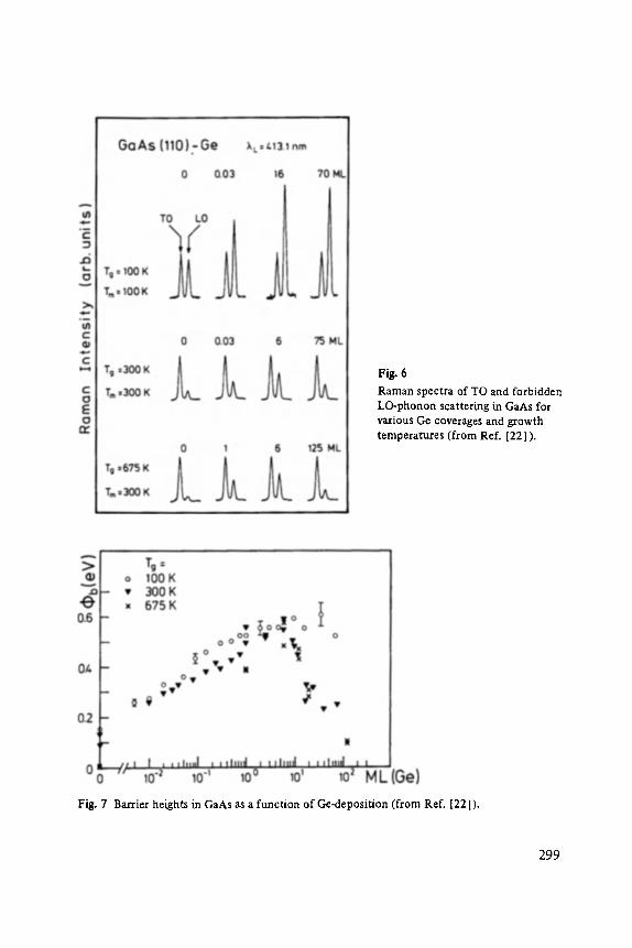
Fie~ 6 Raman spectra of TO and forbidden LO-phonon scattering in GaAs for various Ge coverages and growth temperatures (from Ref. [22]).
Fig. 7 Barrier heights in GaAs as a function of Ge-deposition (from Ref. [221).
299
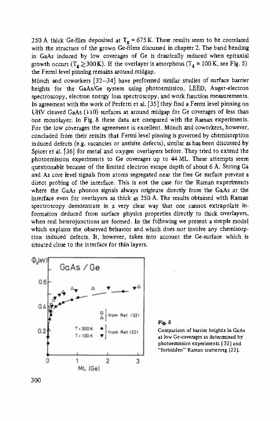
250 A thick Ge-film deposited at Tg = 675 K. These results seem to be correlated with the structure of the grown Ge-films discussed in chapter 2. The band bending in GaAs induced by low coverages of Ge is drastically reduced when epitaxial growth occurs (Tg ~300K) . If the overlayer is amorphous (Tg = 100 K, see Fig. 5) the Fermi level pinning remains around midgap.
M6nch and coworkers [32-34] have performed similar studies of surface barrier heights for the GaAs/Ge system using photoemission, LEED, Auger-electron spectroscopy, electron energy loss spectroscopy, and work function measurements. In agreement with the work of Perfetti et al. [35] they find a Fermi level pinning on UHV cleaved GaAs (110) surfaces at around midgap for Ge coverages of less than one monolayer. In Fig. 8 these data are compared with the Raman experiments. For the low coverages the agreement is excellent. M6nch and coworkers, however, concluded from their results that Fermi level pinning is governed by chemisorption induced defects (e.g. vacancies or antisite defects), similar as has been discussed by Spicer et al. [36] for metal and oxygen overlayers before. They tried to extend the photoemission experiments to Ge coverages up to 44 ML. These attempts seem questionable because of the limited electron escape depth of about 6 A. Strong Ga and As core level signals from atoms segregated near the free Ge surface prevent a direct probing of the interface. This is not the case for the Raman experiments where the GaAs phonon signals always originate directly from the GaAs at the interface even for overlayers as thick as 250 A.. The results obtained with Raman spectroscopy demonstrate in a very clear way that one cannot extrapolate in- formation deduced from surface physics properties directly to thick overlayers, when real heterojunctions are formed. In the following we present a simple model which explains the observed behavior and which does n o t involve any chemisorp- tion induced defects. It, however, takes into account the Ge-surface which is situated close to the interface for thin layers.
Fig. 8 Comparison of barrier heights in GaAs at low Ge-coverages as determined by photoemission experiments [32] and "forbidden" Raman scattering [22].
300
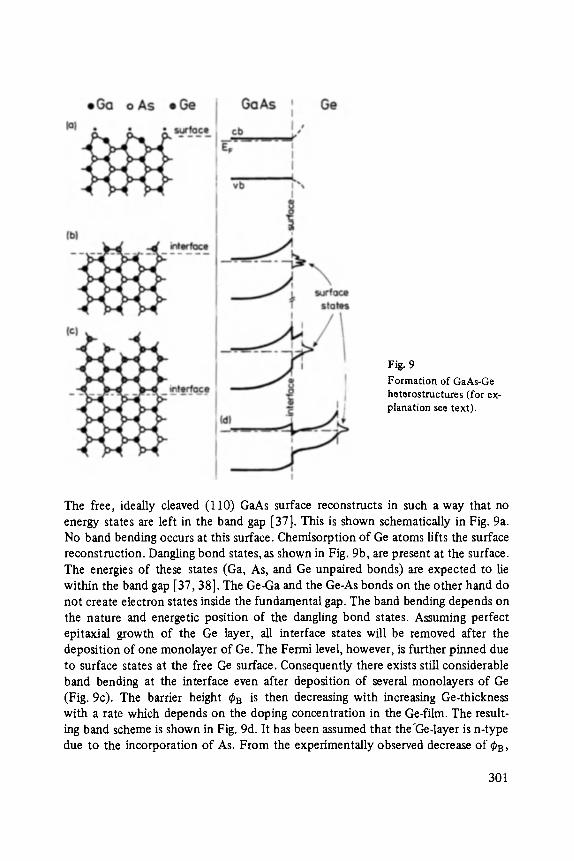
Fig. 9 Formation of GaAs-Ge heterostructures (for ex- planation see text).
The free, ideally cleaved (110) GaAs surface reconstructs in such a way that no energy states are left in the band gap [37]. This is shown schematically in Fig. 9a. No band bending occurs at this surface. Chemisorption of Ge atoms lifts the surface reconstruction. Dangling bond states, as shown in Fig. 9b, are present at the surface. The energies of these states (Ga, As, and Ge unpaired bonds) are expected to lie within the band gap [37, 38]. The Ge-Ga and the Ge-As bonds on the other hand do not create electron states inside the fundamental gap. The band bending depends on the nature and energetic position of the dangling bond states. Assuming perfect epitaxial growth of the Ge layer, all interface states will be removed after the deposition of one monolayer of Ge. The Fermi level, however, is further pinned due to surface states at the free Ge surface. Consequently there exists still considerable band bending at the interface even after deposition of several monolayers of Ge (Fig. 9c). The barrier height q~B is then decreasing with increasing Ge-thickness with a rate which depends on the doping concentration in the Ge-film. The result- ing band scheme is shown in Fig. 9d. It has been assumed that the'Ge.layer is n-type due to the incorporation of As. From the experimentally observed decrease of CB,
301
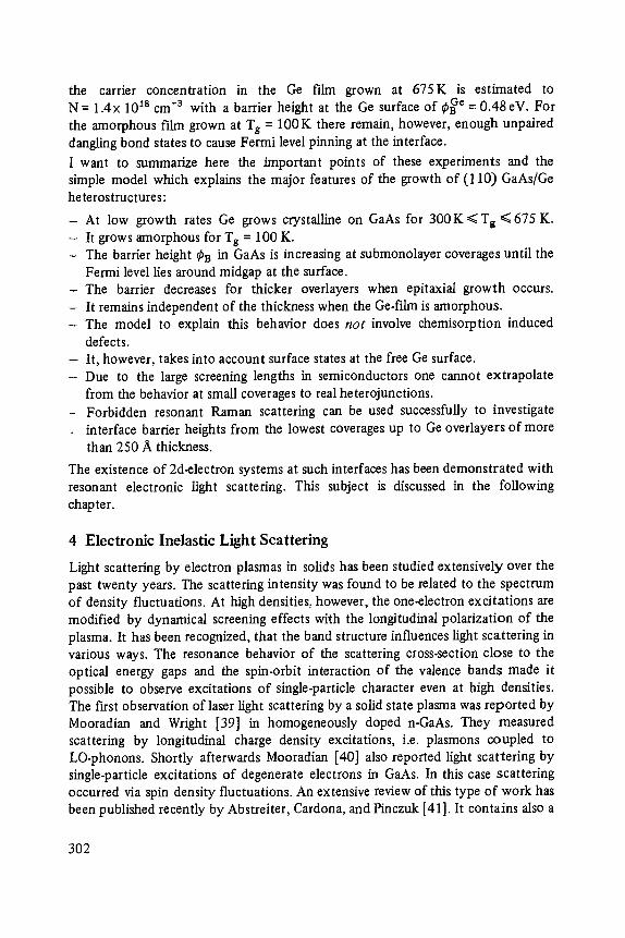
the carrier concentration in the Ge film grown at 675K is estimated to N = l a x 10 is cm -3 with a barrier height at the Ge surface of ~ e = 0.48eV. For the amorphous film grown at Tg = 100K there remain, however, enough unpaired dangling bond states to cause Fermi level pinning at the interface.
I want to summarize here the important points of these experiments and the simple model which explains the major features of the growth of (110) GaAs/Ge heterostructures:
- At low growth rates Ge grows crystalline on GaAs for 3 0 0 K K T g K675 K. - It grows amorphous for Tg = 100 K. - The barrier height eB in GaAs is increasing at submonolayer coverages until the
Fermi level lies around midgap at the surface. - T h e barrier decreases for thicker overlayers when epitaxial growth occurs. - It remains independent of the thickness when the Ge-film is amorphous. - The model to explain this behavior does not involve chemisorption induced
defects. - It, however, takes into account surface states at the free Ge surface. - Due to the large screening lengths in semiconductors one cannot extrapolate
from the behavior at small coverages to real heterojunctions. - Forbidden resonant Raman scattering can be used successfully to investigate
interface barrier heights from the lowest coverages up to Ge overlayers of more than 250 A thickness.
The existence of 2d-electron systems at such interfaces has been demonstrated with resonant electronic light scattering. This subject is discussed in the following chapter.
4 E lec t ron ic Inelast ic Light Scat ter ing
Light scattering by electron plasmas in solids has been studied extensively over the past twenty years. The scattering intensity was found to be related to the spectrum of density fluctuations. At high densities, however, the one-electron excitations are modified by dynamical screening effects with the longitudinal polarization of the plasma. It has been recognized, that the band structure influences light scattering in various ways. The resonance behavior of the scattering cross-section close to the optical energy gaps and the spin-orbit interaction of the valence bands made it possible to observe excitations of single-particle character even at high densities. The first observation of laser light scattering by a solid state plasma was reported by Mooradian and Wright [39] in homogeneously doped n-GaAs. They measured scattering by longitudinal charge density excitations, i.e. plasmons coupled to LO-phonons. Shortly afterwards Mooradian [40] also reported light scattering by single-particle excitations of degenerate electrons in GaAs. In this case scattering occurred via spin density fluctuations. An extensive review of this type of work has been published recently by Abstreiter, Cardona, and Pinczuk [41]. It contains also a
302

chapter on resonant inelastic light scattering by 2d-systems. The large resonan- ce enhancement of spin-flip single-particle and collective excitations observed in n-GaAs around the Eo + Ao energy gap [42] led to the suggestion that light scattering might be sensitive enough to investigate the elementary excitations of 2d-systems at semiconductor surfaces or interfaces [42, 43]. The proposal was soon followed by the first observation of resonant light scattering by intersubband excitations between discrete energy levels of electrons in GaAs/(AlxGal_x)As heterostructures [44]. Indeed, light scattering turned out to be an excellent method for the investigation of single-particle and collective excitations in 2d-carrier sys- tems. In subsequent studies this technique has been applied to study subband splittings and coupling to LO-phonons, which give directly Coulomb matrix ele- ments of the electronic levels involved, in semiconductor structures such as GaAs/(AlxGal_x)AS single and multiple heterostructures [45-49], GaAsdoping superlattices [50, 51], GaAs/Ge heterostructures [52], metal-insulator-semicon- ductor structures involving InP [53], InAs [54, 55], and Si [56, 57]. The limited space in the present article allows only the discussion of basic principles of light scattering in 2d-systems and of some selected experiments. The interested reader is referred to Ref. [41] with most of the relevant references therein.
It has been pointed out by Burstein et al. [58] that, within the effective mass approximation, the mechanisms and selection rules for resonant light scattering by a 2d-electron plasma are similar to those of 3d-systems. 2d-systems, however, are characterized by the separation of motion perpendicular and parallel to the direction of quantization (normal to the interface). In the parallel direction the usual dispersion of the bands is maintained. Normal to the interface the carriers are bound in subbands with minimum energies Co, el , e2,... The total energy is given by
E = ei + - - i= 0, 1,2 .... (4) 2m*
Fig. 10 shows schematically a heterojunction potential well, the subbands co, el, e2, and their dispersion in kll. EF is the Fermi energy. It is chosen such that only the lowest subband is occupied. Depending on the scattering wavevector q one can create both intra- and inter-subband excitations. These are indicated by arrows. Excitations within one subband are only possible, if there exists a sufficiently large component of ~ in the ~n direction. Similar to the three-dimensional case one can separate single-particle and collective excitations. The collective intrasubband excitations are two-dimensional plasma oscillations of the carriers parallel to the interface. The energy tends to zero with decreasing q II. Such excitations have been observed in GaAs/(AlxGal_x)As multilayer structures [59]. The dispersion of these modes is shown schematically in Fig. 11 together with the intrasubband single-particle excitations and with collective and single-particle intersubband excitations.
303

Fig. 10 Potential well and k ii-dispersion of subbands at semiconductor hetero- junctions. Also shown are intra- and intersubband excitations relevant for light scattering experiments.
Fig. 11 k~-dispersion of electronic ex- citations in two-dimensional carrier systems (schematically).
In the backscattering geometry applied usually, the component of ~ in the ~ll- direction is negligibly small. Thus mainly intersubband excitations have been in- vestigated so far. Single-particle excitations are vertical transitions of electrons below the Fermi energy in a lower subband to an empty state in a higher subband. Similar to the three-dimensional case, these unscreened excitations are observed under resonance conditions when scattering occurs via spin-density fluctuations. The measured energies correspond directly to the subband splitting. An additional component of the wavevector parallel to the interface leads to a strong broadening of these spin-flip single-particle intersubband excitations as indicated in Figs. I0 and 11. Collective intersubband excitations reflect in a way the finite extension of the carrier system in the direction of quantization. They involve charge density fluctuations and are consequently screened dynamically by Coulomb interactions. This screening causes a shift to higher energies which is also called "depolarization shift". It describes the dielectric response of the thin layer of carriers to the sub- band excitation and can be written as an "effective" plasma frequency co~ normal to the interface. If only two levels are involved, one finds [60-62] :
2Nse 2 co~ 2 = hese----- ~ COol fll (5)
where fll is the matrix element of the Coulomb interaction of the two subbands, Ns is the 2d-carrier concentration in the lowest occupied subband, and co01 is the bare energy splitting (el -Co) . The collective subband excitation is then given by
~*~ = co021 + co~: (6)
304
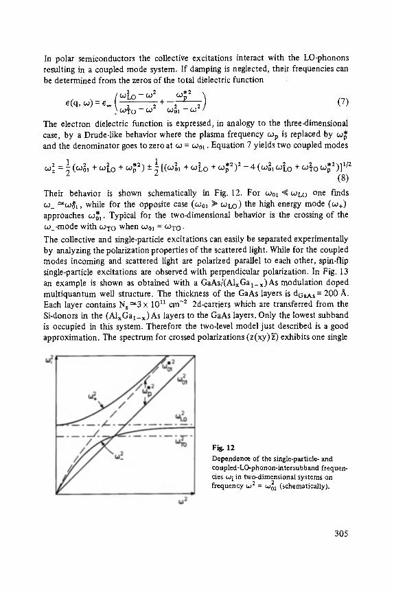
In polar semiconductors the collective excitations interact with the LO-phonons resulting in a coupled mode system. If damping is neglected, their frequencies can be determined from the zeros of the total dielectric function
+(q, co) = + . \ co+-- co + 7 / (7)
The electron dielectric function is expressed, in analogy to the three-dimensional case, by a Drude-like behavior where the plasma frequency cop is replaced by co~ and the denominator goes to zero at ~: = cool �9 Equation 7 yields two coupled modes
1 z 1 c ~ : ) u 2 2 2 *2 1/2 = - (r COLO + ~)TO COp )1 co~ ~ (co0, + W~O + co~2) + ~ [(co~l + coCO + - 4
(8) Their behavior is shown schematically in Fig. 12. For cool "~ co~.o one finds c o ~co~l, while for the opposite case (6o0, ~" COLO) the high energy mode (co+)
�9 Typical for the two-dimensional behavior is the crossing of the approaches coo~. co_-mode with COTO when co01 = COTO.
The collective and single-particle excitations can easily be separated experimentally by analyzing the polarization properties of the scattered light. While for the coupled modes incoming and scattered fight are polarized parallel to each other, spin-flip single-particle excitations are observed with perpendicular polarization. In Fig. 13 an example is shown as obtained with a GaAs/(AlxGal_x)As modulation doped multiquantum well structure. The thickness of the GaAs layers is dGaAs = 200 A. Each layer contains Ns=*3 x 10 ~ crn -2 2d-carriers which are transferred from the Si-donors in the (AlxGal-x)As layers to the GaAs layers. Only the lowest subband is occupied in this system. Therefore the two-level model just described is a good approximation. The spectrum for crossed polarizations (z(xy) z-) exhibits one single
Fig. 12 Dependence of the single-particle- and eoupled-LO-phonon-intersubband frequen- cies to i in two-dimensional systems on frequency to 2 = ~oo21 (schematically).
305

Fig. 14 Single-particle spectrum from a selectively doped GaAs/Ge he terostructure (from Ref. [521).
Fig. 13
Electronic Raman spectra of a modulation doped GaAs/(AlxGal_x) As heterostructure.
peak labeled r which lies on top of a hot-luminescence background. This peak is assigned to spin-flip sinlge-particle intersubband excitations between the two lowest subbands. The energy is in excellent agreement with self-consistent calculations [63]. The parallel polarized spectrum (z(yy)z-) shows three peaks, a sharp LO- phonon line originating from the surface depletion layer, and the coupled modes ca_ and co+. From the energies of these modes we deduce co~ = 16.7 meV and f t t = 10A which compares well with model-calculations for this systems r = 11.5 A). These types of spectra have been measured for various systems "11
in order to determine quantitatively subband splittings, co~, and the Coulomb matrix elements fnn. Ill GaAs doping superlattices it was also possible to change the system from 2d to 3d behavior [51]. In these systems the carrier concentration is easily tunable via photoexcitation.
Recently the first results of light scattering studies of electrons confined to GaAs/Ge interfaces have been reported [52]. The GaAs band gap is larger than the band gap of Ge. Therefore charge transfer leads to 2d-carriers in Ge. Merlin et al. [52] used differences in the resonant behavior of the light scattering intensities to assign features as arising from the Ge or the GaAs layers. The resonant optical gap for electronic Raman scattering in Ge is the E1 gap which is 2.22 eV. The samples
306
investigated consist of a thin Ge-layer (=*300 A) grown with MBE on top of a (100) n-GaAs substrate. Spectra with crossed polarizations exhibit a broad asym- metric structure which peaks around 25 meV. An example is shown in Fig. 14. The resonant behavior of this peak indicates a well-defined resonance for photon energies close to the E1 -gap of Ge. It unambiguously identifies the scattering to be associated with the Ge-layer. The broad line is interpreted as transitions from a single occupied subband state to a 3d free-electron-like continuum. The band scheme for such an accumulation layer is shown in the insert. The interpretation is supported by a calculation of the lineshape of the z (x 'y ' )~ spectrum assigned to spin-density fluctuations. A fit to a broadened one-dimensional density of states is shown by the solid line in Fig. 14. It applies when the 2d- and 3d-like subbands have the same effective mass for the in-plane motion. ~o is the binding energy of the single occupied subband. It is in good agreement with the calculated subband energy. These experiments are the first spectroscopic evidence that it is possible to create 2d-electron systems at the GaAs/Ge interface. It further supports the con- clusion drawn from the "forbidden" phonon scattering experiments which have been discussed in chapter 3.
5 Final Remarks
The usefulness of inelastic light scattering for the investigation of various properties of semiconductor heterojunctions and superlattices has been demonstrated. It is a non-destructive spectroscopic technique with high spatial resolution. The scattering processes are well understood, so that it can act now as a powerful tool to charac- terize and analyse electrical and optical properties of new materials. Resonant Raman scattering experimentswill certainly be used in the future to obtain informa- tion during the growth procedure, but also to investigate the properties of sophisti- cated new types of heterojunctions and multilayer systems, which are of interest with respect to technological applications. These involve graded junctions, spike doped layers, burried channels, especially tailored structures whose achievement requires advanced crystal growth techniques. All this together may be called in a fashionable way "band structure engineering".
Acknowledgements
Most of the work discussed here was a collaborative effort in our group in Munich. It is a pleasure to mention especially H. Brugger, F. Schtiffler, and Ch. Zeller whose contributions can also be identified from the cited references. I also want to mention the excellent coopera- tion with K. Ploog and his group at the MPI fur FestkSrperforschung in Stuttgart. The work has been supported by the Deutsche Forschungsgemeinschaft via SFB 128.
307
References
[1] L. Esakiand R. Tsu, IBM J. Res. Develop. 14, 61 (1970). [2] R. Dingle, in "Festk6rperprobleme", ed. by H.J. Queisser (Vieweg, Braunschweig,
1975), Vol. XV, p. 21. [3] L.L. Chang and L. Esaki, Surf. Sei. 98, 70 (1980). [4] K. Ploogand G. H. D6hler, Adv. Phys. 32, 285 (1983). [5] T. Ando, A. B. Fowler, and F. Stern, Rev. Mod. Phys. 52, 437 (1982). [6] R. Dingle, H. L. St6rrner, A. C. Gossard, and W. Wiegmann, Appl. Phys. Lett. 33, 665
(1978). [7] H.L. St6rmer, J. Phys. Soc. Jap. 49 (Suppl. A), 1013 (1980). [8] K.v. Klitzing, G. Dorda, andM. Pepper, Phys. Rev. Lett. 45,494 (1980). [9] D. C. T~ui, H. L. St6rmer, and A. C. Gossard, Phys. Rev. B25, 1405 (1982).
[10] D. C. Tsui, H. L. St6rmer, andA. C. Gossard, Phys. Rev. Lett. 48,494 (1982). [11] R.L . Anderson, Solid State Electron. 5,341 (1962). [12] IV. R. Frensley and H. Kroemer, Phys. Rev. B15, 2642 (1977). [13] IV. Harrison, J. Vac. Sci. Technol. 14, 1016 (1977). [14] G.A. Baraff, J. A. Appelbaum, and D. R. Hamann, Phys. Rev. Lett. 38, 237 (1977).
[15] IV. E. Pickett, S. G. Louie, andM. L. Cohen, Phys. Rev. B17,815 (1978). [16] J. Pollmann and S. T. Pantelides, Phys. Rev. B21,709 (1980). [17] E.A. Kraut, R. IV. Grant, J.R. IValdrop, and S. P. Kowalczyk, Phys. Rev. Lett. 44,
1620 (1980). [18] A.D. Katnani and G. Margaritondo, Phys. Rev. B28, 1944 (1983). [19] R. Loudon, Adv. Phys. 13,423 (1964). [20] G. Ab~treiter, E. Bauser, A. Fischer, and K. Ploog, Appl. Phys. 16,345 (I978). [21] M. Cardona in "Light Scattering in Solids II", Topics in AppL Phys. 50, eds. M. Cardona
and G. G~ntherodt (Springer, Heidelberg, 1982), p. 19. [22] H. Brugger, F. Schiiffler, and G. Abstreiter, Phys. Rev. Lett. 52,141 (1984). [23] R. Trommer, G. Abstreiter, and M. Cardona, in Proc. of the Intern. Conf. on Lattice
Dynamics, ed. M. Balkanski (Flammazion, Paris, 1977), p. 189. [24] A.A. Gogolin andE. Z Rashba, Solid State Commun. 19, 1177 (1976). [25] A. Pinczuk and E. Burstein, Phys. Rev. Lett. 21, 1073 (1968). [26] d. G. Gay, J. D. Dow, E. Burstein, and A. Pinczuk, in Light Scattering in Solids, ed.
M. Balkanski (Flammarion, Paris, 1971), p. 33. [27] F. Sch;Tffler, Thesis, Teehn. Univ. Miinchen (1984). [28] H. Z Stolz and G. Abstreiter, Solid State Commun. 36,857 (1980). [29] H. Z Stolz and G. Abstreiter, in Proc. 15 th Int. Conf. on the Physics of Semiconductors,
Kyoto (1980); J. Phys. Soc. Jap. 49, (Suppl. A), 1101 (1980). [30] H. Z Stolz and G. Abstreiter, J. Vac. Sci. Technol. 19,380 (1981). [31] F. Scha'ffler and G. Abstreiter, in "Surface Studies with Lasers", Springer Series in
Chemical Physics 33, 131 (1983). [32] IV. M6nch and H. Gant, J. Vac. Sci. Technol. 17, 1094 (1980). [33] IV. M6nch and H. Gant, Phys. Rev. Lett. 48, 512 (1982). [34] IV. M6nch, R. S. Bauer, H. Gant, andR. Murschall, J. Vac. Sci. Technol. 21,498 (1982).
308
[35] P. Perfetti, D. Denley, K .A . Mills, andD. A. Shirley, Appl. Phys. Lett. 33, 667 (1978). [36] W.E. Spicer, J. Lindau, P. Skeath, C. Y. Su, and Patrick Chye, Phys. Rev. Lett. 44,
420 (1980).
[37] E. a t. Mele andJ. D. Joannopoulos, Phys. Rev. BI7, 1816 (1978).
[38] A. Mazur, P. Pollmann, andM. Sehmeits, Solid State Commun. 36,961 (1980). [39] A. Mooradian and G. B. Wright, Phys. Rev. Lett. 16,999 (1966). [40] A. Mooradian, in Light Scattering Spectra of Solids, ed. G. B. Wright (Springer, Berlin,
Heidelberg, New York, 1969), p. 285. [41] G. Abstreiter, M. Cardona, and A. Pinczuk in "Light Scattering in Solids IV", Topics in
Applied Physics 54, eds. M. Cardona and G. Giintherodt (Springer, Heidelberg, 1984), p.5.
[42] A. Princzuk, G. Abstreiter, R. Trommer, and M. Cardona, Solid State Commun. 30, 429 (1979).
[43] E. Burstein, A. Pinczuk, and S. Buchner, in Physics of Semiconductors, ed. B. L. Wilson (The Institute of Physics, Bristol, London, 1979), p. 585.
[44] G. Abstreiter and K. Ploog, Phys. Rev. Lett. 42, 1308 (1979). [45] A. Pinczuk, H. L. St6rmer, R. Dingle, J. M. Worlock, W. Wiegmann, and A. C. Gossard,
Solid State Commun. 32, 1001 (1979). [46] G. Abstreiter, Surf. Sci. 98, I17 (1980). [47] A. Pinczuk, J. M. Worlock, H. L. St6rmer, R. Dingle, W. Wiegmann, and A. C. Gossard,
Solid State Commun. 36, 43 (1980). [48] G. Abstreiter, Ch. Zeller, and K. Ploog, in Proc. 8 th Intern. Syrup. on GaAs and Related
Compounds, ed, H. W. Thim (The Institute of Physics, London, 1981), p. 741. [49] A. Pinczuk and)'. M. Worlock, Surf. Sci. 113, 69 (1982) and references therein. [50] G. H. Ddhler, H. K~nzel, D. Olego, K. Ploog, P. Ruden, H. J. Stolz, and G. Abstreiter,
Phys. Rev. Lett. 47,864 (1981). [51] Ch. Zeller, B. Vinter, G. Abstreiter, and K. Ploog, Phys. Rev. B26, 2124 (1982). [52] R. Merlin, A. Pinczuk, W. T. Beard, and C. E. E. Wood, J. Vac. Sci. Technol. 21, 516
(1982). [53] G. Abstreiter, R. Huber, G. Trankle, and B. Vinter, Solid State Commun. 47, 651
(1983). [54] L. Y. Ching, E. Burstein, S. Buchner, and H. H. Wieder, in J. Phys. Soc. Jap. 49 (Suppl.
A), 703 (1980). [55] G. Triinkle, Diplomthesis, Techn. Univ. Miinchen (1981). [56] G. Abxtreiter, U. Claesxen, and G. Triinkle, Solid State Commun. 44, 673 (1982). [57] M. Baumgartner, G. Abstreiter, andE. Bangert, J. Phys. C17,1617 (1984). [58] E. Burstein, A. Pinezuk, andD. L. Mills, Surf. Sci. 98,451 (1980). [59] D. Olego, A. Pinczuk, A. C. Gossard, and W. Wiegmann, Phys. Rev. B25, 7867 (1982). [ 60] W.P. Chen, Y. Y. Chert, and E. Burstein, Surf. Sei. 58,268 (1976). [61] S. a t. Allen Jr., D. C. Tsui, and B. Vinter, Solid State Commun. 20, 425 (1976); T. Ando,
Solid State Commun. 21,133 (1977). [62] D. Dahl and L. J. Sham, Phys. Rev. B16,651 (1977). [63] T. Ando and S. Mori, J. Phys. Soc. Jap. 47, 1518 (1979).
309
Festk6rperprobleme X X IV (1984)
High-Speed Homo-and Heterostructure Field-Effect Transistors
Heinrich Dgmbkes and Klaus Heime
Universit~t - Gesamthochschule -- Duisburg, Duisburg, Federal Republic of Germany
Summary: The need for ever increasing switching speeds and frequency limits of integrated circuits has resulted in growing interests in the use of llI-V-semiconductor devices, especially field-effect transistors. In this paper first the present status of commercially available GaAs-MESFETs (homostructure FET) is described. Then means of improving these devices by shrinking the dimensions and increasing the dopant concentrations axe discussed. The possibilities of further improvements by using (AIGa)As/GaAs-heterostructures having a two-dimensional electron gas as channel are explained. Especially the influence of the better transport properties of heterostructures (as compared to homostructures) is discussed. Finally the consequences of higher device speed on integrated circuit performance are demonstrated using a simple circuit example.
1 I n t r o d u c t i o n
The ultimate speed of semiconductor devices is determined by the transport prop- erties of the carriers. Therefore, devices made of several III-V-compounds such as GaAs, InP, Ino.saGao.47As lattice matched to InP and certain quantum-well hetero- structures such as AlxGa t_xAs/GaAs or Ino.s3Gao.47As/Ino.s2Alo.4sAs offer po- tential improvement of the high-speed performance over silicon devices. The ve- locity-electric field characteristics of these materials (Fig. 1) deafly show the superiority of the Ill-V-compounds over silicon with respect to mobility and maxi- mum drift velocity. This is the reason why research and development of field-effect transistors (FET) using Ill-V-materials has attracted considerable interest. Presently discrete GaAs-FETs and small-scale integrated circuits (IC) are commercially available. Microwave and millimeter-wave ICs are mainly used for military appLica- tions, while large-scale digital ICs are ready for the commercial market [1,2] .
Questions and problems under discussion are:
1. Is there a need for devices and circuits with better speed performance than silicon?
2. Is an appropriate material quality achievable?
3. Is sufficiently high production yield and hence sufficiently low cost possible?
Clearly the answers to all three questions must be yes if a broad commercial market is expected. In this context only an answer to question 1 is given. A wide area of appLication where higher speeds are needed is the microwave and millimeter-wave
311

Fig. 1 Velocity - field characteristics of several III-V semiconductors for microwave applications and comparison with silicon
Fig. 2 Atmospheric absorption versus frequency - - Frequency limits of GaAs MESFETs, which are commercially available at present . . . . . Improvements due to optimization of material parameters (e.g. doping in blESFETs) or due
to the use of heterostructures
region ( 1 0 - 1 0 0 GHz). One example is the transmission through the atmosphere (Fig. 2). There are two at tenuat ion minima at 36 and 94 GHz, at t ract ive for long distance transmission (satellite broadcast) and an attenuation maximum a t 62 GHz, which can be used for short distance communication. Presently available GaAs-FETs cover a small part o f this spectrum, only. This paper will show that frequencies up to 100 GHz will be attainable with improved GaAs-MESFETs and (A1Ga)A_s/GaAs-
312
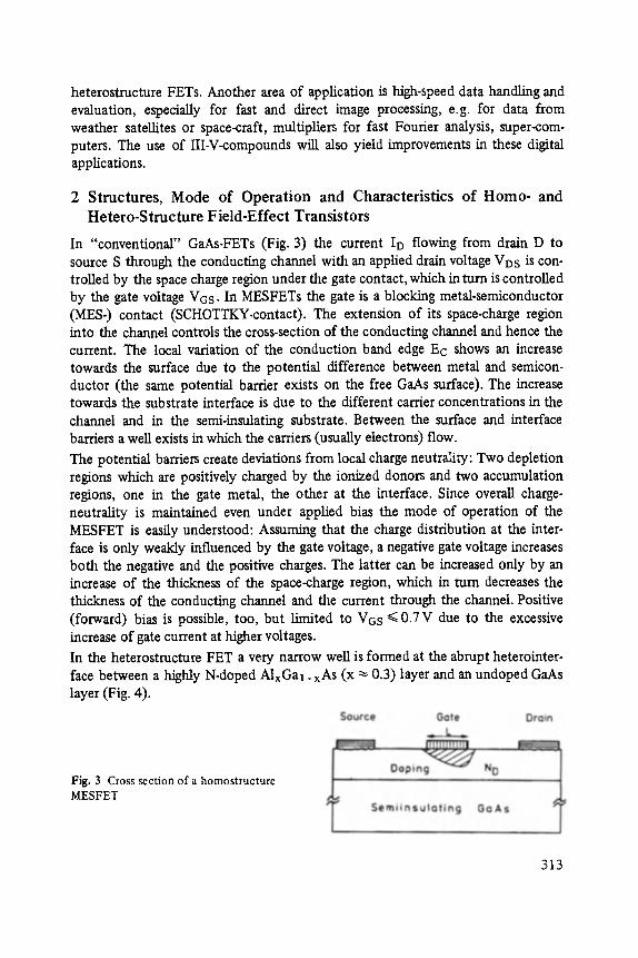
heterostructure FETs. Another area of application is high-speed data handling and evaluation, especially for fast and direct image processing, e.g. for data from weather satellites or space-craft, multipliers for fast Fourier analysis, super-com- puters. The use of III-V-compounds will also yield improvements in these digital applications.
2 Structures, Mode of Operat ion and Characteristics of Homo- and Hetero-Structure Field-Effect Transistors
In "conventional" GaAs-FETs (Fig. 3) the current ID flowing from drain D to source S through the conducting channel with an applied drain voltage VDS is con- trolled by the space charge region under the gate contact, which in mm is controlled by the gate voltage VGS. In MESFETs the gate is a blocking metal-semiconductor (IVIES-) contact (SCHOTTKY-contact). The extension of its space-charge region into the channel controls the cross-section of the conducting channel and hence the current. The local variation of the conduction band edge Ec shows an increase towards the surface due to the potential difference between metal and semicon- ductor (the same potential barrier exists on the free GaAs surface). The increase towards the substrate interface is due to the different carrier concentrations in the channel and in the semi-insulating substrate. Between the surface and interface barriers a well exists in which the carriers (usually electrons) flow.
The potential barriers create deviations from local charge neutrality: Two depletion regions which are positively charged by the ionized donors and two accumulation regions, one in the gate metal, the other at the interface. Since overall charge- neutrality is maintained even under applied bias the mode of operation of the MESFET is easily understood: Assuming that the charge distribution at the inter- face is only weakly influenced by the gate voltage, a negative gate voltage increases both the negative and the positive charges. The latter can be increased only by an increase of the thickness of the space-charge region, which in turn decreases the thickness of the conducting channel and the current through the channel. Positive (forward) bias is possible, too, but limited to VGS <~ 0.7 V due to the excessive increase of gate current at higher voltages. In the heterostructure FET a very narrow well is formed at the abrupt heterointer- face between a highly N-doped AlxGal _xAs (x ~ 0.3) layer and an undoped GaAs layer (Fig. 4).
Fig. 3 Cross section of a homostructure MESFET
313
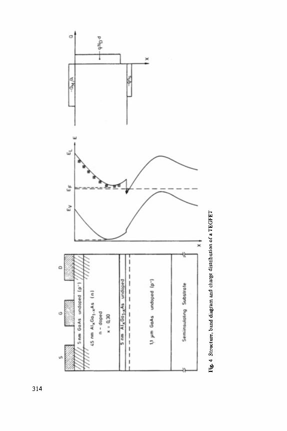
314
[...
r.r.I
0
o
r/l
Electrons are spatially separated from their donor atoms and transferred from the higher band gap material (AlGa)As into the well existing in the undoped lower gap material forming a quasi two-dimensional electron gas since the thickness of this quantum well is very small (~ 10 nm). The main advantage of this configuration over the conventional MESFET is the fact that both high electron concentrations and high mobilities (and velocities) are attained, while in conventional MESFETs the electron concentration is increased by increasing the donor concentration in the channel which consequently reduces the mobility. The current flow through the two-dimensional channel is again controlled by a metal-semiconductor contact. Since electron mobility in (AlGa)As is very low any conduction in this layer has to be suppressed [3, 4]. Therefore the (AlGa)As-layer thickness is chosen such that it is completely depleted of mobile charges by both the metal-semiconductor barrier and the transfer into GaAs. As long as this depletion is maintained an increase of the negative charge in the gate metal by a negative gate bias results in a decrease of the carder concentration in the channel and vice-versa. The mode of operation is similar to that of a conventional MESFET. Presently several notations are used for heterostructure FETs:
- TEGFET (= _two-dimensional _electron gas FET) - SDHT (= _selectively doped heterostructure transistor) - HEMT (= _high _electron mobility transistor) - MODFET (= modulation-doped FET)
The current-voltage characteristics can be calculated from the charge-control mode of operation. With respect to the carrier transport three domains have to be distin- guished:
a) C o n s t a n t m o b i l i t y . d o m a i n
Mobility is constant only ff the electric field in the channel parallel to the current flow is below a certain limit, e.g. less than approximately 3 kV/cm in GaAs or less than 0.5 kV/cm in TEGFETs (cf. Fig. l , 13). Such low fields only exist in long- channel devices (L >/10/sin) or at verylow drain voltages VDS ,e.g. for VDS ~< 0.35 V in GaAs-MESFETs or VDS ~< 0.05 V in TEGFETs, both at L = 1/~rn. In this case the current-voltage characteristic for the saturation region (ID inde- pendent of VDS) is given by
I D = k(VGs- VT) 2
eo �9 er w 1 w k =
VT
CG
(1)
(2)
= gate voltage at which I D = 0 (threshold voltage)
= % . er /d = gate capacitance per area
315
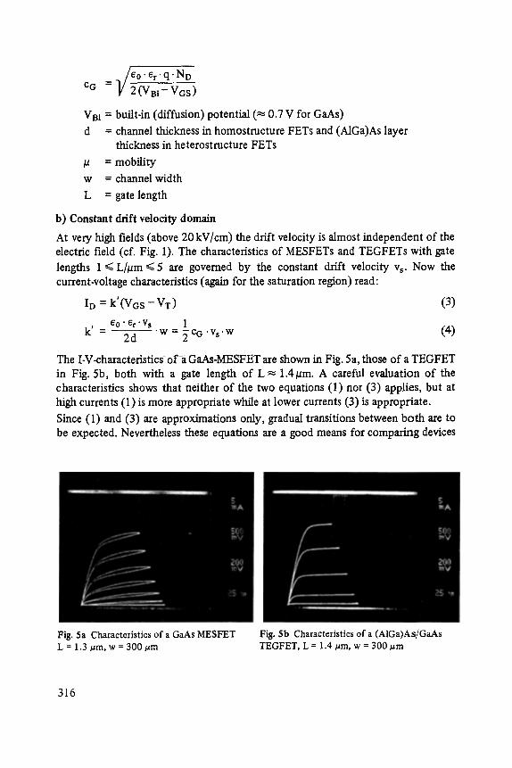
/ e O : e r ' q ' N D
C G = V 2 ( V B i _ V G s )
VBi = built-in (diffusion) potential (~ 0.7 V for GaAs)
d = channel thickness in homostructure FETs and (AlGa)As layer thickness in heterostmcture FETs
p = mobility
w = channel width
L = gate length
b) Constant drift velocity domain
At very high fields (above 20 kV]cm) the drift velocity is almost independent of the electric field (cf. Fig. 1). The characteristics of MESFETs and TEGFETs with gate lengths 1 ~< L/pm ~< 5 are governed by the constant drift velocity vs. Now the current-voltage characteristics (again for the saturation region) read:
ID = k'(VGS - VT) (3)
eo �9 er �9 vs 1 k ! ~__ - - 2d "w = ~ CG" Vs'W (4)
The I-V-characteristics-of-a GaAs-MESFET are shown in Fig. 5a, those of a TEGFET in Fig. 5b, both with a gate length of L ~ 1 A/am. A careful evaluation of the characteristics shows that neither of the two equations (1) nor (3) applies, but at high currents (1) is more appropriate while at lower currents (3) is appropriate.
Since (1) and (3) are approximations only, gradual transitiom between both are to be expected. Nevertheless these equations are a good means for comparing devices
Fig. 5a Characteristics of a GaAs MESFET L = 1.3 gin, w = 300 #m
Fig. 5 b Cha rac t e r i s t i c s o f a ( A 1 G a ) A s / G a A s
T E G F E T , L = 1.4 # m , w -- 3 0 0 ~ m
316
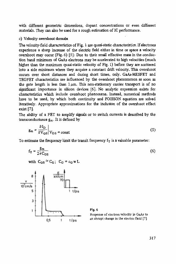
with different geometric dimensions, dopant concentrations or even different materials. They can also be used for a rough estimation of IC performance.
e) Velocity overshoot domain
The velocity-field characteristics of Fig. 1 are quasi-static characteristics. If electrons experience a sharp increase of the electric field either in time or space a velocity overshoot may occur (Fig. 6) [5]: Due to their small effective mass in the conduc- tion band minimum of GaAs electrons may be accelerated to high velocities (much higher than the maximum quasi-static velocity of Fig. 1) before they are scattered into a side minimum where they acquire a constant drift velocity. This overshoot occurs over short distances and during short times, only. GaAs-MESFET and TEGFET characteristics are influenced by the overshoot phenomenon as soon as the gate length is less than 1/am. This non-stationary carrier transport is of no significant importance in silicon devices [6]. No analytic expression exists for characteristics which include overshoot phenomena. Instead, numerical methods have to be used, by which both continuity and POISSON equation are solved iteratively. Appropriate approximations for the inclusion of the overshoot effect exist [7]. The ability of a FET to amplify signals or to switch currents is described by the transconductance gin. It is defined by
0ID g m - ~--~GS VDS = eonst (5)
To estimate the frequency limit the transit frequency fT is a valuable parameter:
gm fT - 2~rCGs (6)
w i t h CGS ~" C G ; C G = c G w L
Fig. 6 Response o f electron velocity in GaAs to an abrupt change in the electric field [7]
317
In the saturation region one obtaines (using (1)-(4)):
constant mobility
gm = 2k(VGs - VT) (7)
w V = cG u E (VGs - T)
ND qpw'd (i _V/2 eo er CV'Bi - VGS)] L qND /
ND gm max ~ --L-" (9)
/AW (VGs _VT ) fT - 27rL 2
/a f ~Lz
andwith /a~ I/V~D 1
fT 2
constant drift velocity
gm '~" ke
= C G "Vs 'W
/_ qNo eo er = v -w v 2WBi--VG)
(11)
(8)
gm max ~ V~D :#: f(L) (i0)
Ys fT = 2~rL (12)
1 fT ~ ~ =/= f(ND)
In MESFETs, ND is the dopant concentration in the channel while in TEGFETs ND is the dopant concentration of the (AlGa)As layer.
With decreasing gate length the constant drift velocity domain is reached. Then the transconduetance is independent of the gate length, but can be increased by the dopant concentration. The transit frequency does not depend on the dopant con- centration because both gm and C G increase with ND (~ V~-DD). However, fT further increases with a reduction of the gate length, because the transit time of the carriers decreases. As soon as velocity overshoot phenomena become important, current, transconductance, and transit frequency are further increased by de- creasing gate length. These influences will be shown in the following chapter.
3 GaAs-MESFETs (Homos t ruc tu re FET): Present Status and Fu t u r e Improvements
Presently gate lengths down to 0.25/~m and doping concentrations o f 1. . . 2 x 10¹⁷crn-3 are used, resulting in FETs with a frequency limit of 70 GHz [8]. The dopant level of 1 ... 2 • 1017 c m -3 is regarded as a good compromise between a high current (and hence high transconductance and frequency limit) and high gate- drain breakdown voltage (and hence high power) and especially a good production yield.
318

However, at the short gate lengths and carrier concentrations mentioned above several new problems arise, summarized as "short-channel effects". These are (Fig. 7):
- An increase of the drain current with drain-source voltage even in the saturation region which results in a reduced voltage amplification
- The threshold voltage VT becomes bias- and gate-length dependent and can no longer be derived from simple formulas, thus preventing an accurate design of devices and ICs.
The main reason for these disadvantageous effects is the fact that the ratio L/d of gate length to channel thickness is no longer much larger than 1 creating a pro- nounced two-dimensional field pattern under the gate. Therefore the potential barrier (Fig. 8) between source and drain is strongly influenced by the drain voltage VDS and this explains why more current flows with increasing VDS. It also explains why the threshold VT becomes bias dependent.
These effects can be reduced or even eliminated if the ratio Lid is maintained much larger than 1 by decreasing the channel thickness d. Since the threshold voltage depends on both channel thickness and doping concentration:
ND d 2 q VT - 2eoe r + Vsi, (13)
a decrease of d has to be accompanied by an increase in ND in order to keep V T --- const.
F i g . 7
Characteristics of a GaAs MESFET showing the negative short channel e ffects: . . . . . calculated according to (1) - - numerical simulation including
two-dimensional field effects and transient transport effects [ 19]
319

Fig. 8 Schematic potential distribution in long and short channel devices [201
Fig. 9 Transconductance of GaAs MESFETs as a function of doping concentration and gate length. (Results of numerical simulations and experimental values [9])
Numerical simulation and experimental work performed by the present authors have shown that a considerable improvement of device performance is possible by simply increasing ND and decreasing d [9].
Fig. 9 displays the transconductance versus doping concentration with the gate length as parameter. A considerable increase is observed for increasing ND even at 1/lm gate length, but it is much more pronounced for shorter gate lengths, showing the positive influence of the velocity overshoot in short-channel devices with L/d >> 1. Experimental results are included in Fig. 9, too. The transit-frequency is
320

Fig. 1o Frequency limit of GaAs MESFETs as function of doping concentration and gate length. (Results of numerical simulations and experimental values [91)
Fig. 11 Characteristics of a GaAs MESFET with a highly doped channel [21] L = 1.2 ~m, w = 300 ~m, gmmax -- 220 mS/ram
shown in Fig. 10. For long gates (L i> 1 gtm) fT is nearly insensitive to the dopant concentration (cf. (12)). For short gates gm increases, but CGs is almost independ- ent of N D because it is mainly a parasitic capacitance determined by the geometric dimensions of the gate metallization.
Figure 10 also shows that the 100 GHz frequency limit is within the reach o f GaAs- MESFETs if the doping concentration is increased over presently used values up to 6 ... 7 x 10¹⁷ era -a for L = 0.25 gra. The device performance even with ND = 10 Is crn -3 is excellent (cf. Fig. 11), showing good saturation and a constant thresh- old voltage. Also the gate-drain breakdown voltage and the gate current are within
321
- - ~ = 1.101ecru -s
--- N O ~ I*lol7cm -3
Fi$. 12 Reverse current of gate diodes for different doping concentrations
the limits which are tolerable for applications (Fig. 12). The results demonstrate very clearly that full advantage of the submicron gate lengths can be taken only if the channel doping is increased over values presently used.
4 Alx Gal -x As/GaAs-TEGFETs (Heteros t ructure FET)
Due to the much shorter history of TEGFETs as compared to MESFETs they are not yet commercially available. Also TEGFETs are not as far optimized as MESFETs already are. However, the experimental results available until now have already shown considerable improvement over conventional MESFETs. This is due to the fact that most of the scattering centers (ionized and neutral impurities) have been removed from the quantum-well channel while the electron sheet concentration is maintained almost as high as in MESFETs.
Therefore the transport properties in the TEGFET are improved, especially at temperatures below room temperature, where the highly doped MESFETs do not show any substantial improvement. The mobility in quantum wells is comparable to pure bulk material (or even better) as shown in Fig. 13. At lower temperatures the low-field mobility increases considerably. However, the high mobility decreases rapidly with increasing electric fields (Fig~ 14), the decrease being more pronounced at lower temperatures. Relatively small fields of I kV/cm (-" 0.1 V/1 #m) are easily achieved in devices. In addition the mobility is not uniform in the channel. From magneto-transconductance measurements (Fig. 15) a mobility profile perpendicular to the interface is measured: Close to the surface (VGs > 0) the mobility is low because of increased scattering by interface roughness and Coulomb interaction with ions in the (AlGa)As layer. At the position of the (AlGa)As/GaAs interface (VGs < 0) /a strongly increases to high values, but then decreases again. The main
322
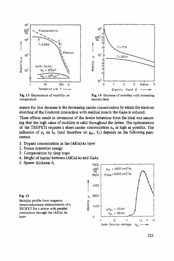
Fig. 13 Dependence of mobility on Fig. 14 Decrease of mobility with increasing temperature electric field
reason for this decrease is the decreasing carrier concentration by which the electron shielding of the Coulomb interaction with residual ions in the GaAs is reduced.
These effects result in deviations of the device behaviour from the ideal one assum- ing that the high value of mobility is valid throughout the device. The optimization of the TEGFETs requires a sheet carrier concentration ns as high as possible. The influence of ns on I D (and therefore on gin, fT) depends on the following para- meters:
1. Dopant concentration in the (AlGa)As layer 2. Donor activation energy 3. Compensation by deep traps 4. Height of barrier between (AlGa)As and GaAs 5. Spacer thickness d i
Fig. 15
Mobility profile from magneto- transconductance measurements of a TEGFET for a device with parallel conduction through the (AlGa) As layer
323
The maximum dopant concentration ND -- 1 ... 2 x 10 xs cm -3 is limited by the growth process. The activation energy of the usual Si donor is sufficiently low to allow full ionization at room temperature, but below 200 K a partial freeze-out of free carriers occurs [3]. From DLTS (Deep-Level Transient Spectroscopy)- and low- frequency noise measurements several traps are known, at least one of which is an intrinsic and possibly uriavoidable defect [10, 11]. Its concentration increases with the Al concentration and may equal the donor concentration at x ~ 0.35 [12]. The band bending in the (AlGa)As towards the interface is ~ 0.2 eV at x -~ 0.35 and depends on the Al-concentration, too. In order to suppress any appreciable reinjec- tion of electrons from the TEG the Al-content should be larger than x = 0.2. These two factors limit the Al-eontent to about 0.2 ... 0.35. In order to reduce the residual Coulomb scattering between the ionized donors and the TEG an undoped (AlGa)As spacer layer of the thickness d i is often introduced between the undoped GaAs and the n+- (AlGa)As. Thereby the electron transfer into the TEG is further reduced but mobility is enhanced. Electrons are transferred from a depth dd ~ 5 ... 10 nm above the hetero interface, while the optimum thickness of the (AlGa) As layer is approximately 45 nm.
Thus less than 30% of the electrons in the (AIGa)As are available for transfer. The maximum sheet carder concentration in practical TEGFET structures therefore is
ns = NO" dd
1 ... 2" 1018 cm -3 .5 ... 10" 10-7cm (14)
~- 5 .10 H ... 2" 1012era -2
In Fig. 16 the correlation between ns, No, and di is given.
Combining the transport properties and the carrier concentrations one obtains transconduetanees and frequency limits shown in Fig. 17 and 18. Experimental
Fig. ~6 Dependence of sheet carrier concentration in a (AIGa) As/ GaAs heterostructttre on doping concentration and spacer thickness
324
Fig. 17 Intrinsic transconductance of TEGFETs as function of doping concentration in the (AlGa)As and spacer thickness Data are calculated for L = 1 vm and T = 300 K
Fig. 18 Frequency limit of TEGFETs calculated for L = 1 #m and T = 300 K
325
Fig. 19 Cross sectional view of improved TEGFET structure and de-characteristics L= 1.4 ~m, w = 150~m
results are included, too. The data shown in Fig. 17 are for intrinsic devices. In actual devices parasitics such as series and contact resistances have to be Included. They reduce the performance of the device to its extrinsic properties. As long as the sheet carrier concentration is ns ~ 1012 cm -2 the parasitics cannot be reduced very much. Therefore additional steps have to be taken. One possibility is an additional n +§ GaAs top layer (Fig. 19), which conducts the current outside the intrinsic device. With a sheet carrier concentration of ns > 10 ~3 cm -2 in the top layer the parasitic resistances are reduced by about one order of magnitude, result- ing in a strongly improved transconductance. At lower temperatures this additions/ top layer may be unnecessary.
5 In tegra ted Circuits Using F ie ld -Ef fec t Transis tors
The two most important parameters for evaluating the performance of digital ICs are the switching time and the power consumed during the switching process. Also the product of these two parameters is a useful figure of merit.
As a simple example an inverter gate (Fig. 20) will be discussed, which is the fun- damental cell of the more complex gates [13, 14]. It consists of a switch formed by the FET and a load. If with logic high voltage at the input the switch is con- ducting the output voltage is logic low and vice versa. Several other gates may be coupled to the output of the inverter. They are simply represented by the load capacitance CL. If the transistor switches from the conducting to the noncon- ducting state (or vice versa) a load current IL flows.
It is now assumed that the logic swing is
Vma x = VQHig h - V Q L o w -- ( V G S - VT)ma x ~ 0.5 VDD.
Further assuming that the optimum mean load current is
I L = 0.5 IDmax and CL = const., one obtaines:
[L = 0"5 k ' "Vmax
326
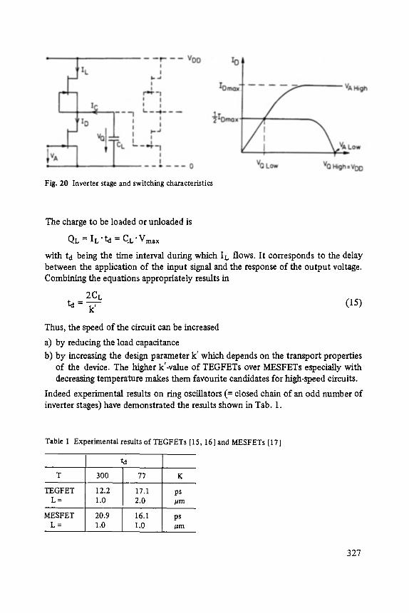
Fig. 20 Inverter stage and switching characteristics
The charge to be loaded or unloaded is
QL = IL ' td = C.L'Vmax
with td being the time interval during which I L flows. It corresponds to the delay between the application of the input signal and the response of the output voltage. Combining the equations appropriately results in
2CL t d - k' (15)
Thus, the speed of the circuit can be increased
a) by reducing the load capacitance
b) by increasing the design parameter k' which depends on the transport properties of the device. The higher k'-value of TEGFETs over MESFETs especially with decrea,~g temperature makes them favourite candidates for high-speed circuits.
Indeed experimental results on ring oscillators (= closed chain of an odd number of inverter stages) have demonstrated the results shown in Tab. 1.
Table 1 Experimental results of TEGFETs [ 15, 161 and MESFETs [ 171
T 3OO
FEGFET 12.2 L = 1.0
MESFET 20.9 L= 1.0
td
77 K
17.1 ps 2.0 ~m
16.1 ps 1.0 ~m
327
The power consumption is approximately
PD = VDD" IL = k"V2max (16)
Equation (16) shows that the power increases with k' such that the power-delay- time product
PD" td = 2CL" V~ax (17)
does not depend on the device properties in this simple approximation. However, better transport properties allow a redesign of the device, for instance a reduction of the device width if the current is to be held constant. Then k' is held constant with respect to the original value but CL (if determined by the input capacitance of the following gates) is reduced. Thus, ta decreases and PD td is reduced propor- tional to the width of the device. A more detailed analysis is given in [ 18 ].
6 Conclus ion
It was the aim of this paper to demonstrate which improvements are possible in the performance of HI-V-semiconductor FETs. First it was shown that conventional GaAs-MESFETs can be improved by increasing the dopant concentration in the channel. Despite a reduction of the mobility the transconductance is increased. Simultaneously disadvantageous short-channel effects are reduced or even elimi- nated. Thus, full advantage of the velocity-overshoot effect can be taken in sub- micron devices. Secondly it was shown that the transport properties of two-dimen- sional electron gas layers are superior to conventional FET layers at room tempera- ture, and even more pronounced at lower temperatures. Therefore TEGFETs have performance advantages over MESFETs. Moreover the noise performance of TEG- FETs is better than that of MESFETs, but the reasons are not completely under- stood until now. Finally some materials (Ino.5 3 Gao.47 As) have even better transport properties. One may therefore expect further improvements in device performance. Due to problems in material growth and device technology the advantages of this last material have not yet been demonstrated with FETs until now.
Acknowledgements
The authors wish to thank the members of this laboratory for their contributions to the work, especially Dipl.-Ing. W. Brockerhoff, Dipl.-Ing. A. Giirke and G. Howahl. The work was partially supported by the Deutsche Forschungsgemeinschaft (MESFETs) and Stiftung Volkswagenwerk (TEGFETs). The cooperation with Dr. K. Ploog and Dipl.-Ing. E. Schubert (Max-Planck-Insti- tut ftir FestkSrperforschung, Stuttgart) within the latter project and with Dr. G. Weimann (For- schungsinstitut der Deutschen Bundespost, Darmstadt) is gratefully acknowledged.
328
References
[1] N. Yokoyama, T. Ohnishi, H. Onodera, T. Shinoki, A. Shibatomi, and H. Ishikawa: A GaAs 1K Static RAM Using Tungsten Silicide Gate Self-Aligned Technology. IEEE Journ. Solid State Circ., Vol. SC-18 (1983) No. 5, pp. 520 -524
[2] N. Nakayama, K. Suyama, H. Shirnizu, iV. Yokoyama, H. Ohnishi, A. Shibatomi, and H. Ishikawa: A GaAs 16 X 16 Bit Parallel Multiplier. IEEE Journ. Solid State Circ., Vol. SC-18 (1983) No. 5, pp. 599-603
[3] E. F. Schubert, K. Ploog, H. Diirnbkes, and K. Heime: Selectively Doped n-AlxGa 1 . xAs/ GaAs Heterostructures with High-Mobility Two-Dimensional Electron Gas for Field Effect Transistors. Part I. Effect of Parallel Conductance. Appl. Phys. A 33 (1984), pp. 63 -76
[41 K. Lee, M. Shur, T.J. Drummond, and H. Morkoc: Parasitic MESFET in (A1Ga)As/GaAs Modulation Doped FETS and MODFET Characterization. IEEE Trans. on Electron Devices, Vol. ED:31 (1984) No. 1, pp. 29 -34
[5] E. Constant: Modeling of Sub-Micron Devices. Inst. Phys. Conf. Set. No. 57 (1980), pp. 141-168
[6] A. Yoshii, M. Tornizawa, and K. Yokoyama: Accurate Modeling for Submicrometer-Gate Si and GaAs MESFETs Using Two-Dimensional Particle Simulation. IEEE Trans. on Electron Devices, Vol. ED-30 (1983) No. 10, pp. 1376-1380
[71 B. Carnez, A. Cappy, A. Kaszynski, E. Constant, and G. Salmer: Modeling of a Sub- micrometer Gate Field-Effect Transistor Including Nonstationary Electron Dynamics. Appl. Phys., Vol. 51 (1980) No. 1, pp. 784-790
[8] E. T. Watkins, J. M. Sehellenberg, L. H. Hacket, Y. Yarnasaki, and M. Feng: A 60 GHz GaAs FET Amplifier. IEEE MTT-S 1983 Digest, pp. 145-147, June 1983
[91 14. Diimbkes, Ir Brockerhoff K. Heime, and A. Cappy: Improved Short Channel GaAs MESFETs by Use of Higher Doping Concentration to be publ. in IEEE Trans. on Electron Devices, Vol. ED-31 (1984) No. 7
[I0] L. Loreck, H. Diimbkes, K. Heime, K. Ploog, and G. Weimann: Deep-Level Analysis in (A1Ga)As-GaAs 2D-Electron Gas Devices by Means of Low Frequency Noise Measure- ments. IEEE Electron Devices Letters, VoL EDL-5 (1984) No. 1, pp. 9 -11
[11] K. Hikosaka, T. Mirnura, and S. Hiyamizu: Deep Electron Traps in MBE-Grown A1GaAs Ternary Alloy for Heterojunction Devices. Inst. Phys. Conf. Ser. No. 63 (1981), pp. 233 -238
[12] B. L. Zhou, K. Ploog, E. Gmelin, X. Q. Zheng, and M. Schulz: Assesment of Persistent- Photoconductivity Centers in MBE-Grown AlxGa 1 _ xAs Using Capacitance Spectroscopy Measurements. Appl. Phys. A 28 (1982), pp. 223-227
K. Lehovec and R. Zuleeg: Analysis of GaAs FETs for Integrated Logic. IEEE Trans. on Electron Devices, Vol. ED-27 (1980) No. 6, pp. 1074-1091
R. C. Eden, B. M. Welch, R. Zucca, and S. I. Long: The Prospects for Ultrahigh-Speed VLSI GaAs Digital Logic. IEEE Journ. Solid State Circ., Vol. SC-14 (1979) No. 2, pp. 221-239 C P. Lee, D. Hou, S. Lee, D. Miller, and R. Anderson: Ultra High Speed Digital Integrated Circuits Using GaAs/GaA1As High Electron Mobility Transistors. IEEE GaAs IC Syrup. 1983, Digest, pp. 162-165
[16] T. Mimura, K. Joshin, and S. Kuroda: Device Modeling of HEMTs. Fujitsu Scient. & Techn. Journal, Vol. 19 (1983) No. 3, pp. 243-278
[t3l
It4]
It51
329
[17] R.A. Kiehl, P. G. Flahive, S.H. Wemple, and H.M. Cox: Direct-Coupled GaAs Ring Oscillators with Self-Aligned Gates. IEEE Electron Device Letters, Vol. EDL-3 (1982) No. 11, pp. 325-326
[18] D. Delagebeaudeuf and N. T. Linh: Speed Power in Planar Two-Dimensional Electron Gas FET DCFL Circuit: A Theoretical Approach. Electronics Letters, Vol. 18 (1982) No. 12, pp. 510-512
[19] Y. Awano, K. Tomizawa, N. Hashizume, and M. Kawashima: Monte Carlo Particle Simulation of GaAs Short-Channel MESFETs. Electronics Letters, Vol. 19 (1983) No. 1, pp. 20-21
[201 J.F. Pone, R. C. Castagne, J. 1". Courat, and C. Arnodo: Two-Dimensional Particle Modeling of Submicrometer Gate GaAs FETs near Pinchoff. IEEE Trans. on Electron Dev. Vol. ED-29 (1982) No. 8, pp. 1244-1255
[21] H. D~mbkes: HersteUung und Eigenschaften yon GaAs Schottky-Gate Feldeffekttran- sistoren mit Kan~ilen hoher Elektronenkonzentration. Dissertation, Universit~it Duisburg, 1983
330
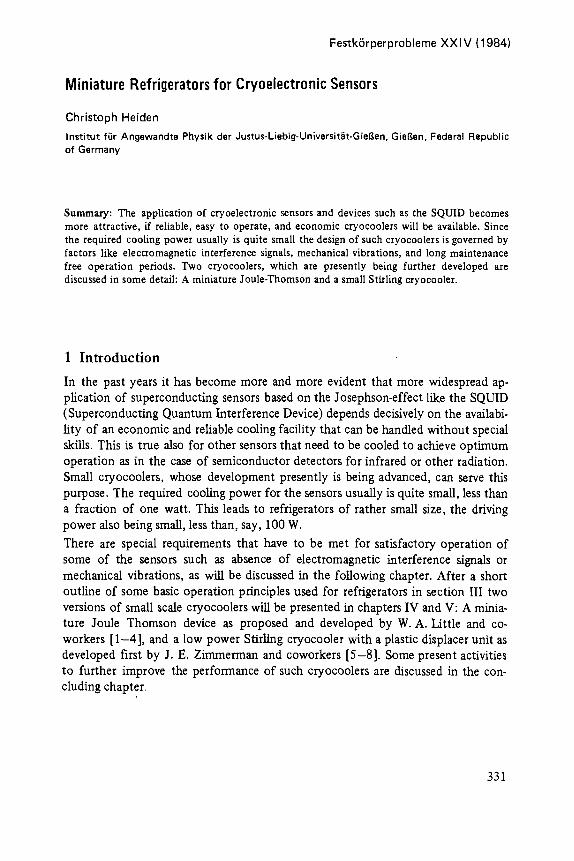
FestkSrperprobleme XXIV (1984)
Miniature Refrigerators for Cryoelectronic Sensors
Christoph Heiden
Institut fiir Angewandte Physik der Justus-Liebig-Universit~t-Giel~en, Giel~en, Federal Republic of Germany
Summary: The application of cryoelectronic sensors and devices such as the SQUID becomes more attractive, if reliable, easy to operate, and economic cryocoolers will be available. Since the required cooling power usuaUy is quite small the design of such cryocoolers is governed by factors like electromagnetic interference signals, mechanical vibrations, and long maintenance free operation periods. Two cryocoolers, which are presently being further developed are discussed in some detail: A miniature Joule-Thomson and a small Stifling cryocooler.
1 I n t r o d u c t i o n
In the past years it has become more and more evident that more widespread ap- plication o f superconducting sensors based on the Josephson-effect like the SQUID (Superconducting Quantum Interference Device) depends decisively on the availabi- lity of an economic and reliable cooling facility that can be handled without special skills. This is true also for other sensors that need to be cooled to achieve optimum operation as in the case of semiconductor detectors for infrared or other radiation. Small cryocoolers, whose development presently is being advanced, can serve this purpose. The required cooling power for the sensors usually is quite small, less than a fraction of one watt. This leads to refrigerators of rather small size, the driving power also being small, less than, say, 100 W.
There are special requirements that have to be met for satisfactory operation of some of the sensors such as absence of electromagnetic interference signals or mechanical vibrations, as will be discussed in the following chapter. After a short outline of some basic operation principles used for refrigerators in section III two versions o f small scale cryocoolers will be presented in chapters IV and V: A minia- ture Joule Thomson device as proposed and developed by W. A. Little and co- workers [1 -4] , and a low power Stirling cryocooler with a plastic displacer unit as developed first by J. E. Zimmerman and coworkers [5-8] . Some present activities to further improve the performance of such cryocoolers are discussed in the con- cluding chapter.
331
2 Cryocoo le r Specif icat ions
Depending on device and application the cryocoolers have to meet different speci- fications regarding operating temperature, cooling power and other factors such as maintenance free working periods.
Temperatures in the range of 50 K-100 K usually are sufficient for photo-con- ducting radiation detectors like those on the basis of Cdx Hgl-xTe or InSb, needing a cooling power of the order of mW or less. However, if a short cool down time is required the cooling power usually will be dictated by the heat capacity of the material used in the cryocooler, and may be Considerably larger.
For most superconducting devices the required cooling power is even less. Sensors incorporating one or several Josephson contacts have a dissipation of the order of 1 nW to 100 nW. Depending on the material, temperatures between 4 K and ca. 20 K are needed.
A rather severe requirement results from the extreme sensitivity of SQUIDs for magnetic flux, the best devices presently exhibiting a spectral noise limit of the order of 10 -6 ~o Hz -I/2 where 4~o = h/2e is the flux quantum [9, 10]. The SQUID is also a very attractive sensor for other quantities that can be transformed into magnetic flux by suitable transducers. Even if one does not use the highest possible sensitivity magnetic fields originating from the cryocooler have to be kept as small as possible. Mechanical vibrations also should be reduced to a minimum since a SQUID-sensor which i s vibrating in an external magnetic field will register a cor- responding magnetic ac-flux.
The requirements with regard to interference noise from the cryocooler in many cases certainly can be relaxed to some extent if ac-signals are to be detected by the superconducting sensors. The use of a dc-SQUID as a low noise preamplifier for frequencies up to the GHz range appears possible. First results with noise tempera- ture near one Kelvin at 100 MHz and a power gain of ca. 20 db have been reported recently [11 ]. To be mentioned is also the use of a resistive dc-SQUID as a hetero- dyne receiver for electromagnetic Waves in the region of millimeter and submilli- meter waves as well as are in general detectors on the basis of the ac-Josephson effect like oscillators or voltage standards [12]. Again less restrictive with regard to magnetic background signals is a class of devices like the quasiparticle SIS-mixer (Superconductor-Insulator-Superconductor) [13] or potential multielectrode devices like the QUITERON (Quasiparticle Injection Tunneling Effect) [ 14] that are based on non equilibrium phenomena of superconductivity.
This list of cryoelectronic sensors is far from complete. There is no mention of superconducting paramps, super-Schottky diodes, bolometers [ 15-17 ] nor o f devices which exhibit a higher degree of integration like logic circuits. The refrigeration power for all these devices is very low, in most cases for stationary operation below one watt. Their application potential would be increased considerably by the availability of refrigeration systems that are reliable, economical, and easy to operate for the non-specialist.
332
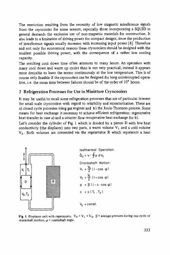
The restriction resulting from the necessity of low magnetic interference signals from the cryocooler for some sensors, especially those incorporating a SQUID in general demands the exclusive use of non-magnetic materials for construction. It also leads to a limitation of driving power for compact designs, since the production of interference signals usually increases with increasing input power [8]. Therefore and not only for economical reasons these cryocoolers should be designed with the smallest possible driving power, with the consequence of a rather low cooling capacity.
The resulting cool down time often amounts to many hours. An operation with many cool down and warm up cycles then is not very practical, instead it appears more desirable to leave the sensor continuously at the low temperature. This is of course only feasible if the cryocoolers can be designed for long uninterrupted opera- tion, i.e. the mean time between failures should be of the order of 104 hours.
3 Ref r ige ra t ion Processes fo r Use in Minia ture Cryocoo le r s
It may be useful to recall some refrigeration processes that are of particular interest for small scale cryocoolers with regard to reliability and miniaturization. These are a) closed cycle processes using gas engines and b) the Joule-Thomson process. Some means for heat exchange is necessary to achieve efficient refrigeration: regenerative heat transfer in case a) and a counter flow recuperative heat exchange for b).
Let's consider the cylinder of Fig. 1 which is divided by a piston D with low heat conductivity (the displacer) into two parts, a warm volume V1 and a cold volume V2. Both volumes are connected via the regenerator R which represents a heat
Fig. I Displacer unit with regenerator. Vo = V1 + V2, P = average pressure during one cycle of crankshaft motion, ~ = crankshaft anne.
333

storage unit with the following properties: large heat capacity, good heat exchange with and low flow resistance for the working gas, and low heat conductivity in the direction of gas flow. If the displacer is moved upward gas with temperature T1 passes R and is thereby cooled to the lower temperature T2. Since the system has constant volume the pressure p will drop during this process. If D is moved down- ward the opposite will take place increasing temperature und pressure of the gas. In an ideal situation with negligible friction of the displacer seals and zero flow resistance in the regenerator the motion of D can be performed without work since the pressure on both sides of D is the same. If the motion of D is controlled by a crankshaft the relations given in Fig. 1 are obtained with the factor c being deter- mined by the equation of state of the working gas. The cooling power Qz for the isothermal process is given by
(~2 = v ~ pdV2
where v is the frequency of the displacer movement. Inserting the expressions of Fig. 1 yields of course Q2 = 0 since no work is done.
In order to obtain a nonzero cooling power, additional pressure variations as func- tion of displacer position have to be generated. Some possibilities are shown in Fig. 2.
Fig. 2 Principle of Stirling, Vuilleumier, and Gifford-McMahon gas engines [ 7]. Q1, Q2, W = heat at hot or cold end and mechanical work, resp.
334
1. Stirling process: located in a fraction of the warm volume is a compressor piston, whose movement lags that of the displacer by 90 ~ Note that in Fig. 2 the regenera- tor has been incorporated into the displacer [18].
2. Vuilleumier process: Instead of using a mechanical compressor one also can use a thermal compressor made of a second displacer-regenerator unit [19].
3. Gifford-McMahon process: in this process the pressure variations are generated by varying the total mass of the working substance in the system. This is achieved by connecting the displacer unit at the right phase angles with one or the other side of a compressor.
All these processes are at least in principle well suited for cryocoolers with long trouble free operation. There are no valves in the Stifling and Vuilleumier process. The valves of a Gifford-McMahon machine are at room temperature and can easily be serviced. It is therefore no wonder that intensive development has taken place recently involving all three of these processes, Gifford McMahon being used with much success to provide refrigeration in cryopump units [20], Vuilleumier as a source for refrigeration in space operating with solar heat requiring almost no driving power for the displacer motion [21], and Stirling, when driving power is not at premium as in terrestrial applications for cryoelectronic devices.
The Joule-Thomson cooler depicted in Fig. 3 also exhibits features that make it an attractive choice for small reliable cryocoolers since except for the compressor it contains no movable mechanical parts. Instead of a compressor also cylinders with compressed gas can be used. Cooling is achieved by expanding the real gas below its inversion temperature through the throttle valve, the counter flow heat exchanger providing a positive feedback. Without external heat load liquefaction of the work- ing gas easily can be achieved.
4 Microminia ture Cryocoo le r s Using the Jou le T h o m s o n E f f ec t
As indicated above, designs according to Fig. 3 allow rather compact constructions, and small refrigerators were built already many years ago [21-23]. Although rather successful in performance, these refrigerators have not found widespread use a)
Fig. 3 Principle of Joule-Thomson cryocooler.
335

since the throughput of high pressure gas was of the order 10 barliters/min, which limits the operation time from a standard cylinder of compressed gas to a few hours and b) since high gas pressures of the order of 100 bar and more are required to obtain acceptable efficiencies. Closed cycle operation, therefore, became unattractive due to the cost of the high pressure compressors.
W. A. Little considered in 1977 the possibility to reduce the size of these refrigera- tors such that their cooling power assumes levels more appropriate for cryoelec- tronic devices, i.e. 100 mW and less instead of a few watts. From a simple scaling analysis it became clear that the tubing diameter of the corresponding heat ex- changer had to be reduced to the order of 0.1 mm and less which led to the idea to use, similar as for the fabrication of large scale integrated circuits (LSI), photo- lithography as a means to produce the needed fine channels and nozzles [1 ].
In the following years, microminiature refrigerators were successfully developed along these lines. The fabrication process starts with etching the channel structure for the heat exchanger, throttle, and liquid reservoir (boiler) into a thin glas plate (cf. Fig. 4). To avoid underetching, the channels are cut by a micro sandblasting technique with 27 tam diam. A12 03 powder entrained in a high velocity gas stream. To do this a special photoresist had to be developed that was able to withstand the abrasive action of the gas stream. Fig. 5 shows a SEM-picture of a portion of the heat exchanger channels. Glas is used for its low thermal conductivity and high mechanical strength. To seal the channels, a coverplate glas slide is glued or fused on top of the etched plate, carefully avoiding clogging of the channels. Inlet and outlet holes then are drilled to which stainless steel hypodermic tubing for the entering and outgoing gas is glued with epoxy.
The entire assembly is enclosed in a removable vacuum chamber providing electrical feedthrough for the devices to be cooled. A typical cool down curve for such a re- frigerator operating with 120 bar nitrogen and a gas throughput of 1.2 bar. l/min is shown in Fig. 6 giving a cooling power of 250-500 roW. Lower flow rates of about 0.1 to 0.2 bar'//min have been achieved [3] with refrigerators having a cooling power of 25 to 50 mW at 87 K. Small portable gas cylinders thus can be used still giving sufficient operation time for many applications.
Fig. 4 Channel structure of microminiature J.-T. cryocooler [2]. Inlet and outlet parts (a), heat exchanger (b), capillary expansion system (c), and reservoir (d).
336
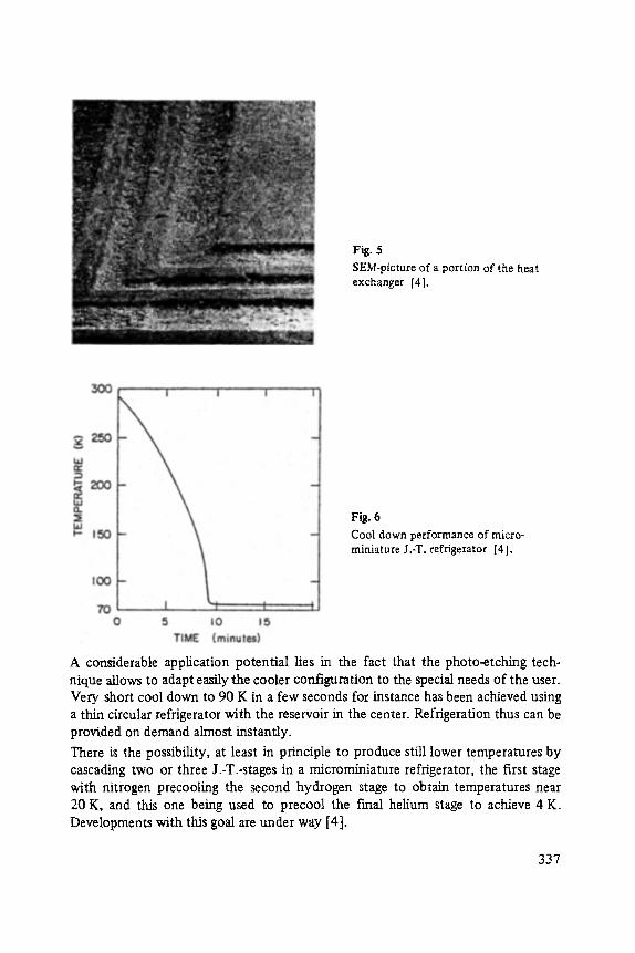
Fig. 5 SEM-picture of a portion of the heat exchanger [4].
Fig. 6 Cool down performance of micro- miniature J.-T. refrigerator [41.
A considerable application potential lies in the fact that the photo-etching tech- nique allows to adapt easily the cooler configuration to the special needs of the user. Very short cool down to 90 K in a few seconds for instance has been achieved using a thin circular refrigerator with the reservoir in the center. Refrigeration thus can be provided on demand almost instantly.
There is the possibility, at least in principle to produce still lower temperatures by cascading two or three J.-T.-stages in a microminiature refrigerator, the first stage with nitrogen precooling the second hydrogen stage to obtain temperatures near 20 K, and this one being used to precool the final helium stage to achieve 4 K. Developments with this goal are under way [4].
337

A "conditio sine qua non" for a satisfactory operation in the purity of the working gas. Thus, nitrogen gas with 99,998 % purity, which is passed through a drier con- taining molecular sieve and a 3 micron particulate f'flter before entering the re- frigerator is used to prevent the channels from clogging after short working periods. The purity requirement is still worse for the hydrogen and helium stages since cooled charcoal or zeolite traps would have to be used to remove N2 or O~ impuri- ties from the working gas.
5 Small Scale Stirling Cryocoolers
At the time of this writing temperatures sufficiently low for superconducting sen- sors have been reached with multistage small scale Stifling cryocoolers due to the pioneer work ofJ. E. Zimmerman and coworkers [8].
Fig. 7 shows one of the first units reaching a temperature low enough to cool a SQUID. Following the philosophy outlined in section 2, compressor piston and displacer unit are made of nonmagnetic plastic materials, nylon or glas fiber rein- forced epoxy. Regenerative heat exchange is achieved in the narrow radial gap be- tween displacer and surrounding cylinder. The displacer unit is divided into four sections, with the result that cooling occurs at the different step locations. This is
338

Table 1 Dimensions and performance of several small plastic cryocoolers [8]
Lowest Temperature Compressor Displacement (cc) Diam./Length - Stage 1 (both in ram) Stage 2
Stage 3 Stage 4 Stage 5
Stroke (mm) Temperature - Stage 1
Stage 2 Stage 3 Stage 4 Stage 5
1-Stage 3-Stage 4-Stage 5-Stage
50K
9.6/300
12.7 50K
13K 38 19/245 9.45/143 4.7/144
12.7 120 K 40K 13K
8.5 K 38 28/150 19/120 9.5/100 4.7/150
7 180 K
8.5 K
7K 9O 38/140 29/130 19/120 9.5/83 4.8/133 7 167 K 70 K 27 K
15.5 K 7K
This machine was operated with valves by compressed gas (i.e., Gifford-McMahon cycle).
an effective measure to reduce the heat input to the cold end a) via conduction along the displacer and the cylinder walls and b) due to the nested radiation shields that are attached to the different steps. The action of these shields is enhanced by superinsulation placed between them. This whole assembly is surrounded by a vacuum can.
A cold end temperature of 8.5 K was attained by using an average helium gas pres- sure of 5 bar, the whole unit being driven by a 50 watt motor at a stroke frequency of I Hz. The piston displacement was 38 cm 3 and the displacer stroke only 7 ram.
Table I lists dimensions and performance of several small cryocoolers one of which having a five step displacer thereby reaching a final temperature around 7 K. Cool- ing power as function of temperature for the cold end of this latter machine is shown in Fig. 8.
Magnetic interference signals were low enough to operate a SQUID for magneto- cardiography although a periodic background signal with the displacer stroke fre- quency was visible [26]. Many thousand hours of operation also have shown that such refrigerators can be built with sufficient reliability.
With regard to long uninterrupted runs some development efforts still appear to be necessary. A "conditio sine qua non" is again the purity of the working gas and for long continuous operation measures have to be taken to prevent it from contamina- tion. Simple O-Ring seals for the compressor piston and displacer shafts are insuffi- cient. Double O-Ring seals with a helium buffer volume in between are better, but were found to lead eventually also to impurities in the gas, which freeze out in the displacer unit causing increased friction, reduced efficiency, and rising temperature
339
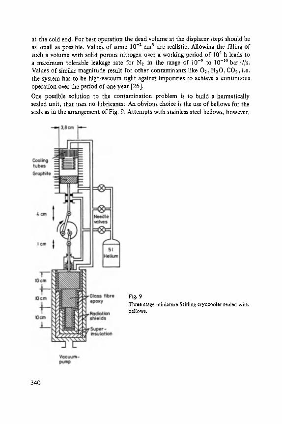
at the cold end. For best operation the dead volume at the displacer steps should be as small as possible. Values of some 10 -2 cm 3 are realistic. Allowing the filling of such a volume with solid porous nitrogen over a working period of 104 h leads to a maximum tolerable leakage rate for N~ in the range of 10 -9 to 10 - I~ bar.l/s. Values of similar magnitude result for other contaminants like 02, H20, CO2, i.e. the system has to be high-vacuum tight against impurities to achieve a continuous operation over the period of one year [26].
One possible solution to the contamination problem is to build a hermetically sealed unit, that uses no lubricants: An obvious choice is the use of bellows for the seals as in the arrangement of Fig. 9. Attempts with stainless steel bellows, however,
Fig. 9 Three stage miniature Stirling cryocooler sealed with bellows.
340
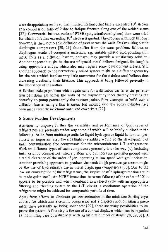
were disappointing owing to their limited lifetime, that barely exceeded l0 s strokes at a compression ratio of 2 due to fatique fracture along one of the welded seams [27]. Commercial bellows made of PTFE (polytetrafluorethylene) then were tried for which a lifetime exceeding 108 strokes is quoted. The problem with such bellows, however, is their noticeable diffusion of gases across the walls. Designs using plastic diaphragm compressors [28, 29] also suffer from the same problem. Bellows or diaphragms made of composite materials, e.g. suitable plastic incorporating thin metal foils as a diffusion barrier, perhaps, may provide a satisfactory solution. Another approach might be the use of special metal bellows designed for long life using appropriate alloys, which also may require some development efforts. Still another approach to the hermetically sealed system might be a different geometry for the seals which involves very little movement for the stainless steel bellows thus increasing drastically their lifetime. This approach is being followed presently in the laboratory of the author.
A further leakage problem which again calls for a diffusion barrier is the penetra- tion of helium gas across the walls of the displacer cylinder thereby creating the necessity to pump permanently the vacuum jacket. First attempts to build such a diffusion barrier using a thin titanium foil molded into the epoxy cylinder have been made recently by Zimmerman and coworkers [29].
6 Some Further Developments
Activities to improve further the versatility and performance of both types of refrigerators are presently under way some of which will be briefly outlined in the following. Aside from multistage units for liquid hydrogen or liquid helium temper- atures, an important step towards higher versatility would be the development of small contamination free compressors for the microminiature J.-T. refrigerators: Work on different types of such compressors presently is under way [4], including small ceramic compressors, whose pistons and cylinders are precision ground with a radial clearance of the order of pan, operating at low speed with gas lubrication. Another promising approach to produce the needed high pressure gas stream might be the use of hydraulically driven metal diaphragm compressors [30]. Due to the low gas consumption of the refrigerators, the amplitude of diaphragm motion could be made quite small. An MTBF (meantime between failures) of the order of 104h appears to be possible and when combined in a closed cycle with an appropriate filtering and cleaning system in the J.-T. circuit, a continuous operation of the refrigerator might be achieved for comparable periods of time.
Apart from efforts to eliminate gas contamination in the miniature Stirling cryo- coolers for which also a ceramic compressor and a displacer motion using a pneu- matic drive presently are being under test [29], there are many possibilities to im- prove the system. A first step is the use of a conical displacer which can be regarded as the limiting case of a displacer with an infinite number of stages [28, 29, 31 ]. A
341
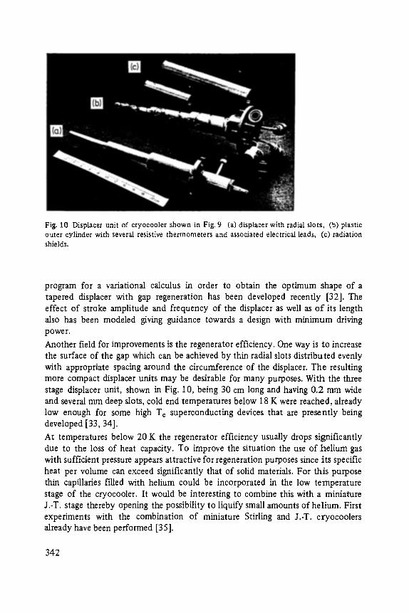
Fig. 10 Displacer unit of cryocooler shown in Fig. 9 (a) displacer with radial slots, (b) ptastic outer cylinder with several resistive thermometers and associated electrical leads, (c) radiation shields.
program for a variational calculus in order to obtain the optimum shape of a tapered displacer with gap regeneration has been developed recently [32]. The effect of stroke amplitude and frequency of the displacer as well as o f its length also has been modeled giving guidance towards a design with minimum driving power.
Another field for improvements is the regenerator efficiency. One way is to increase the surface of the gap which can be achieved by thin radial slots distributed evenly with appropriate spacing around the circumference of the displacer. The resulting more compact displacer units may be desirable for many purposes. With the three stage displacer unit, shown in Fig. 10, being 30 cm long and having 0.2 mm wide and several mm deep slots, cold end temperatures below 18 K were reached, already low enough for some high T c superconducting devices that are presently being developed [33, 34].
At temperatures below 20 K the regenerator efficiency usually drops significantly due to the loss of heat capacity. To improve the situation the use of helium gas with sufficient pressure appears attractive for regeneration purposes since its specific heat per volume can exceed significantly that of solid materials. For this purpose thin capillaries filled with helium could be incorporated in the low temperature stage of the cryocooler. It would be interesting to combine this with a miniature J.-T. stage thereby opening the possibility to liquify small amounts of helium. First experiments with the combination of miniature Stifling and J.-T. cryocoolers already have been performed [35].
342
Further reduction of interference signals also are possible by removing the compres- sor from the displacer unit. For this purpose a Gifford McMahon type o f arrange- ment perhaps might be the more appropriate solution.
As can be seen from these remarks, there is a wide field for improving further the performance of miniature cryocoolers. There is all reason to expect that in the very near future reliable, economical and user-friendly cryocoolers will be available making the product ion of low temperatures for cooling devices a mat ter of throw-
ing a switch.
Acknowledgements
I am indebted to W. A. Little, Stanford University, and J. E. Zimmerman, NBS Boulder, for providing me with their latest results.
References [1 ] IV. A. Little, Applications of Closed-Cycle Cryocoolers to Small Superconducting Devices,
J. E. Zimmerman and T.M. Flynn, eds., NBS Special Publication 508, p. 75 (U.S. Government Printing Office, Washington D.C., 1978).
[2] R. Hollman and W.A. Little, Refrigeration for Cryogenic Sensors and Electronic Systems, J. E. Ziramerman, D. B. Sullivan, and S. E. McCarthy, eds., NBS Special Publication 607, p. 160 (U.S. Government Printing Office, Washington, D.C., 1981).
[3] S. Garvey, S. Logan, R. Rowe, and IV. A. Little, Appl. Phys. Lett. 42, 1048 (1983).
(41 IV. A. Little, Rev. Sci. Inst. (1984) to be published. [5] Z E. Zimraerman, R. Radebaugh, and Z D. Siegwarth, Superconducting Quantum Inter-
ference Devices and their Application, H. D. Hahlbom and 1-1. Liibbig, eds., W. de Gruyter, Berlin (1977) p. 287.
[6] Z E. Zimmerman and R. Radebaugh, Application of Closed Cycle Cryocoolers to Small Superconducting Devices, J. E. Zimmerman and T. M. Flynn, eds. NBS Special Publica- tion 508, p. 59 (U.S. Government Printing Office, Washington D.C., 1978).
[7] J.E. Zimmerman, SQUID 80: Superconducting Quantum Devices and their Applications, H. D. Hahlbohm and H. Liibbig, eds., W. de Gruyter, Berlin (1980) p. 423.
18] J.E. Zimmerman and D. B. Sullivan, NBS Technical Note 1049 (U.S. Government Printing Office, Washington, 1982).
[9] An excellent review on SQUIDs is given by J. Clarke, Superconductor Applications: SQUID and Machines, B. B. Schwartz and S. Foner, eds., Plenum Press, New York (1977), p. 67.
[ 10] R . F . Voss, R. B. Saibowitz, A. N. Broers, S. L Raider, M. Knoedter, and J. M. Viggiano, IEEE Trans. on Magn., MAG. 17, 395 (1981).
[11] C. Hilbert and J. Clarke, Appl. Phys. Lett. 43,694 (1983). [121 R. L Kautz, and G. Costabile, IEEE Trans. on Magn., MAG 17,780 (1981). [13] P. L. Richards, T. M. Shen, R. E. Harris, and F. L. Lloyd, Appl. Phys. Lett. 36,480
(1980). [14] S. M. Faris, S. I. Raider, IV. J. Gallagher, and R. E. Drake, IEEE Trans. Mag., MAG 19,
(1983).
343
[15] P. L. Richards, Superconducting Quantum Interference Devices and their Applications, H. D. Hahlbohm and H. Lfibbig, eds., W. de Gruyter, Berlin (1977), p. 323.
[161 Z Clarke, G. J. Hoffer, P. L. Richards, Rev. Phys. Appl. 9, 69 (1974). [t7l M. McColl, M. F. Millea, A. H. Silver, M. F. Bottfer, R. J. Pedersen, and F. L. Vernon Jr.,
IEEE Trans. on Magn., MAG 13,221 (1977). [18] A thorough treatment of Stifling and other types of cryocoolers can be found in G.
Walker, "Cryoeoolers", Vol. 1 and Vol. 2, Plenum Press, New York (1983).
[191 R. Vuilleumier, U.S. Patent No. 1,275,507, (1918). [201 R. Frank, H.-J. Forth, H.-H. Kleim, R. Heisig, K.-H. V61ker, F.-Z Otte, Proc. ICEC 8,
C. Rizzuto, ed., IPC Science and Techn. Press, Guildford, U.K. (1980) p. 365. [211 G. K. PitcherandF. K. duPr~,Adv. Cryog. Eng. 15, 447 (1970).
[221 S.W. Stephens, Infrared Phys. 8, 25 (1968). [23] J.M. Geist and P. K. Lashmet, Adv. Cryog. Eng. 6, 73 (1961).
[24] Z S. Buller, Adv. Cryog. Eng. 16,205, (1971). [251 D. B. Sullivan, J. E. Zimmerman, and J. T. Ires, Refrigeration for Cryogenic Sensors and
Electronic Systems, J. E. Zimmerman, D. B. Sullivan, and S. E. McCarthy, eds., NBS Special Publication 607, p. 186, (U.S. Government Printing Office, Washington, D.C., 1981).
[261 C Heiden, DKV-Tagungsbericht (1982), p. 53, Deutscher Kiilte- u. Kfimatechnischer Verein, Stuttgart, Germany.
[27] Z G. Daunt and C. Heiden, Refrigeration for Cryogenic sensors and Electronic Systems, J. E. Zimmerman, D. B. Sullivan, and S. E. McCarthy, eds., NBS Special Publication 607, p. 141 (U.S. Government Printing Office, Washington D.C., 1981).
[28] K. Myrtle, W. Winter, and S. Gygax, Cryogenics 22,139 (1982). I291 ,~ E. Zimmerman, D. E. Daney, and D. B. Sullivan, Proe. 2. Biennial Conf. on Refrigera-
tion for Cryogenic Sensors and Electronic Systems, NASA Conf. Publ. 2287, p. 95 (1983).
[301 F.E. Altoz and J. R. Eargle, Adv. Cryog. Eng, 5,317 (1960). [311 F.K. du Pr~ and A. Daniels, Proc. XM Int. Congr. of Refrigeration, Wash. D.C.p. 137.
AVI Publ. Co., Inc., Westport Connecticut (1973). 132] D. B. Sullivan, R. Radebaugh, D. E. Daney, and J. E. Zimmerman, Proc. 2. Biennial
Conf. on Refrigeration for Cryogenic Sensors and Electronic Systems, NASA Conf. Publ. 2287, p. 107 (1983).
[33] T. Fu]ita, M. Suzuki, S. lkegawa. T. Ohtsuka, and T. Anayama, Proc. ICEC 9, K. Yasuko- chi, H. Nagano eds., p. 369 (Butterworth, Guildford, U.K. 1982).
[341 H. Rogaila, B. David, J. Riihl, J. Appl. Phys. 1984 to be published. [35] J.E. Zimmerman, private communication.
344

Contents of volumes published previously (Festk6rperprobleme vol. I . . . XXIV)
Author index
volume/page
Abel, s, F., Borenzstein, Y., L6pez-Rios, T., Optical Properties of Discont inuous Thin Films and Rough Surfaces of Silver . . . . . . . . . . . . . . . . . . . . . . . . . . . . . . XXIV,93
Abstreiter, G., Inelastic Light Scattering in Semiconductor Heterostructures . . . . . . . . . XXIV,291 A ckermann, H., see St6ckmann, 11.-J. . . . . . . . . . . . . . . . . . . . . . . . . . . . . . . . XX, 19 Acket, G.A., and M.T. Vlaardingerbroek, Physical Properties o f Transferred-Electron
and Avalanche Microwave Devices . . . . . . . . . . . . . . . . . . . . . . . . . . . . . . . IX,280 Alefeld, G., New Approaches to Energy Conversion by Alternative Working Fluids . . . . . XVIII,53 Alexander, H., und P. Haasen, Die Plastizit~it yon Germanium und Silizium . . . . . . . . . VIII,268 Allan, D. C., see Joannopoulos, J. D . . . . . . . . . . . . . . . . . . . . . . . . . . . . . . . . . XXI,167 Aspnes, D.A., Modulation Spectroscopy with Synchrot ron Radiat ion . . . . . . . . . . . . XVII,235 Authier, B., Poly-CrystaUine Silicon with Columnar Structure . . . . . . . . . . . . . . . . . XVIII,1
Baltz, R. v., und U. Birkholz, Polaronen . . . . . . . . . . . . . . . . . . . . . . . . . . . . . XII,233 Bangert, E., see Bauer, G . . . . . . . . . . . . . . . . . . . . . . . . . . . . . . . . . . . . . . . XXIII,27 Baraff, G.A., Schlater, M., Electronic Structure o f Localized Defects in Covalent
Semiconductors . . . . . . . . . . . . . . . . . . . . . . . . . . . . . . . . . . . . . . . . . XIX,303 Biissler, H., Liquid Crystals . . . . . . . . . . . . . . . . . . . . . . . . . . . . . . . . . . . . . X1,99 Bauer, G., Jantsch, W., Bangert, E., Band Edge Structure of Ferroelectric I V - V I
Compounds . . . . . . . . . . . . . . . . . . . . . . . . . . . . . . . . . . . . . . . . . . . . XXIII,27 B~uerlein, R., Strahlensch~iden in Halbleitern und Halolel teroauelementen . . . . . . . . . . VIII,1 Bauser, E., Crystal Growth from Melt . . . . . . . . . . . . . . . . . . . . . . . . . . . . . . . XXIII,141 Beenakker, J. J. M., The Influence o f Electric and Magnetic Fields on the Transport
Properties o f Polyatomic Dilute Gases . . . . . . . . . . . . . . . . . . . . . . . . . . . . . VIII,276 Beneking, H., Material Engineering in Optoelectronics . . . . . . . . . . . . . . . . . . . . . XVI,195 Betz, H., see Heuberger, A . . . . . . . . . . . . . . . . . . . . . . . . . . . . . . . . . . . . . . XX,259 BiUe, J., Properties of Highly Excited Semiconductors (Experimental Aspects) . . . . . . . XIII,111 Bilz, H., Theorie der Wechselwirkung elektromagnetischer Strahlung mi t
Gi t terschwingungen . . . . . . . . . . . . . . . . . . . . . . . . . . . . . . . . . . . . . . . VI,218 Bilz, H., see Biittner, H. . . . . . . . . . . . . . . . . . . . . . . . . . . . . . . . . . . . . . . . XXIII,13 Birnberg, D., Wannier-Mott Polaritons in Magnetic Fields . . . . . . . . . . . . . . . . . . . . XVII,195 Binder, K., Theory of Spin Glasses: A Brief Review . . . . . . . . . . . . . . . . . . . . . . . XVII,55 Birkholz, U., see Baltz, R. v . . . . . . . . . . . . . . . . . . . . . . . . . . . . . . . . . . . . . XII,233 Bittel, H., Grunds~itzliches fiber das Problem des Rauschens . . . . . . . . . . . . . . . . . . 1,202 B6er, K. W., Feld- und Strominhomogenit~iten bei hohen elektrischen Belastungen in
Isolatoren und Photoleitern . . . . . . . . . . . . . . . . . . . . . . . . . . . . . . . . . . . 1,38 B6er, K. W., Large Scale Energy Utilization - The Use of Thin Film Solar Cells . . . . . . . XVI,315 Bonnet, D., Selders, M., and H. Rabenhorst, Solar Cells and Their Terrestrial
Applications . . . . . . . . . . . . . . . . . . . . . . . . . . . . . . . . . . . . . . . . . . . XVI,293
345
Bonse, U., Synchro t ron X-Rays for Solid State Physics . . . . . . . . . . . . . . . . . . . . . XXIII,77
Borenzstein, Y., see Abelbs, F. . . . . . . . . . . . . . . . . . . . . . . . . . . . . . . . . . . . XXIV,93 Bosse, Z, see Gabriel, H. . . . . . . . . . . . . . . . . . . . . . . . . . . . . . . . . . . . . . . XII,505 Brenig, W., Theorie elektrortischer Eigenschaften amorpher Substanzen . . . . . . . . . . . XI,175 Brenig, W., Chemisorpt ion o f H, O and CO on Transit ion Metals . . . . . . . . . . . . . . . . X'VII,301 Broser, I., Exzi tonen-Lumineszenz in Halbleitern . . . . . . . . . . . . . . . . . . . . . . . . V,283 Bross, H., Zur Theorie der elektrlschen Lei tungserseheinungen in Halbleitern und
Metallen . . . . . . . . . . . . . . . . . . . . . . . . . . . . . . . . . . . . . . . . . . . . . . V,73 Bfittner, H., Properties of Highly Excited Semiconductors (Theoretical Aspects) . . . . . . XIII,145 Biittner, H., Bilz, H., Nonlinear Structures in Solid State Physics . . . . . . . . . . . . . . . XXIII,13
Campagna, M., see Kisker, E. . . . . . . . . . . . . . . . . . . . . . . . . . . . . . . . . . . . . XIX,259 Cardona, M., Faraday Rotat ion in Semiconductors . . . . . . . . . . . . . . . . . . . . . . . 1,72 Cardona, M., Modulation Spectroscopy of Semiconductors . . . . . . . . . . . . . . . . . . . X,125 Claus, R., Polaritonen (Experiment) . . . . . . . . . . . . . . . . . . . . . . . . . . . . . . . . XII,381 Collet, M. G., and L.J.M. Esser, Charge Transfer Devices . . . . . . . . . . . . . . . . . . . . XIII,337 Conradt, R., Auger-Rekombinat ion in Halbleitern . . . . . . . . . . . . . . . . . . . . . . . . XII,449 Czaja, W., Isoelectric Impurities in Semiconductors . . . . . . . . . . . . . . . . . . . . . . . XI,65 Czulius, W., Z~hldioden und Z~ihltransistoren . . . . . . . . . . . . . . . . . . . . . . . . . . II,216
Diimbkes, H., Heirne, K., High-Speed Homo- and Heterostructure Field-Effekt Transistors . . . . . . . . . . . . . . . . . . . . . . . . . . . . . . . . . . . . . . . . . . . . XXIV,311
Danielmeyer, H. G., Stoichiometric Laser Materials . . . . . . . . . . . . . . . . . . '. . . . . XV,253 Dederichs, P.H., Zeller, R., Electronic Structure of Impurit ies in Transit ion Metals . . . . . XXI,243 Deeg, E., Zusammenhang zwischen Glasstruktur und physikalischen G l a s e i g e n s c h a f t e n . . . IV,119 Dieterich, W., Dynamics o f Fast Ion Conductors . . . . . . . . . . . . . . . . . . . . . . . . . XXI,325 Dingle, R., Confined Carrier Quan t um States in Ultra thin Semiconductor
Heterostructures . . . . . . . . . . . . . . . . . . . . . . . . . . . . . . . . . . . . . . . . . XV,21 DOhler, G.H., n-i-p-i Doping Superlattices - Tailored Semiconductors with Tunable
Electronic Properties . . . . . . . . . . . . . . . . . . . . . . . . . . . . . . . . . . . . . . . XXIII,207 Dohm, V., Folk, R., Critical Dynamics near the X-Transition in 4He . . . . . . . . . . . . . XXII,1 Dorda, G., Surface Quantizat ion in Semiconductors . . . . . . . . . . . . . . . . . . . . . . . . XIII,215 Dormann, E., Kern-Spin-Echo-Messungen an magnet isch geordneten Substanzen . . . . . . XII,487 Dornhaus, R., Surface Enhanced Raman Spectroscopy . . . . . . . . . . . . . . . . . . . . . XXlI,201 Dransfeld, K., see Hunklinger, S. . . . . . . . . . . . . . . . . . . . . . . . . . . . . . . . . . . XVI,267 Druyvesteiyn, W.F., see de Jonge, F.A . . . . . . . . . . . . . . . . . . . . . . . . . . . . . . . XII,531 Ducloy, M., Nonlinear Optical Phase Conjugat ion . . . . . . . . . . . . . . . . . . . . . . . . XXII,35 Duke, C.B., Organic Solids: Traditional Semiconductors or Fermi Glasses? . . . . . . . . . XXII,21
Eastman, L. F., Very High Electron Velocity in Short Gallium Arsenide Structures . . . . . XXII,173 Eggert, H., Zur Beweglichkeit yon Stromtr~igern in Halbleitern . . . . . . . . . . . . . . . . . 1,274 Ehrhart, P., Haubold, H.-G., and hi. Schilling, Investigation o f Point Defects and Their
Agglomerates in Irradiated Metals by Diffuse X-Ray Scattering . . . . . . . . . . . . . . XIV,87 Eichler, H.J., Forced Light Scattering at Laser-Induced Gratings - a Method for
Investigation o f Optically Excited Solids . . . . . . . . . . . . . . . . . . . . . . . . . . . XVIII,241 Eilenberger, G., Ergebnisse und M~ingel der heut igen Theorie der Supraleiter 2. Art . . . . . VIII,254 Elsiisser, K., Kinetische Beschreibung der ,Schwachen Turbulenz ' . . . . . . . . . . . . . . . )(1,28 l Entel, P., see Grewe, N. . . . . . . . . . . . . . . . . . . . . . . . . . . . . . . . . . . . . . . . XX,413 Esser, L.J.M., see Collet, M. G. . . . . . . . . . . . . . . . . . . . . . . . . . . . . . . . . . . . XIII,337 Ewert, S., Inelastic Electron Tunnel ing Spectroscopy . . . . . . . . . . . . . . . . . . . . . . XXIV,73
3 4 6
Felderhoff, B. U., Stochiastic Models in the Theory of Phase Transitions . . . . . . . . . . . XI,293 Fischer, B., see Lagoix, J. . . . . . . . . . . . . . . . . . . . . . . . . . . . . . . . . . . . . . . XVIII,197 Fischer, H., Physics and Technology of Photovoltaic Solar Energy Conversion . . . . . . . . XIV,153 Fischer, 1-1., Solar Cells Based on Nonsinglr Crystalline Silicon . . . . . . . . . . . . . . . . . XVIIl,19 Fischer, R., Radiative Recombination in Amorphous Semiconductors . . . . . . . . . . . . XVII,85 Folberth, O. G., Monolithische Speicher . . . . . . . . . . . . . . . . . . . . . . . . . . . . . . IX,340 Folk, R., see Dohm, V. . . . . . . . . . . . . . . . . . . . . . . . . . . . . . . . . . . . . . . . XXII,1 Forstmann, F., Low-Energy Electron Diffraction for Surface Structure Analysis . . . . . . XIII,275 Forstrnann, F., Gerhardts, R.R., Metal Optics Near the Plasma Frequency . . . . . . . . . . XXII,291 Frank, W., Self-lnterstitials and Vacancies in Elemental Semiconductors
Between Absolute Zero and the Temperature of Melting . . . . . . . . . . . . . . . . . . XXI,221 Fr6hlich, D., 2-Photonenspektroskopie in FestkSrpern . . . . . . . . . . . . . . . . . . . . . X,227 Fr6hlich, D., Aspects of Nonlinear Spectroscopy . . . . . . . . . . . . . . . . . . . . . . . . XXI,363 Fr6hlich, D., see ~Velling, H. . . . . . . . . . . . . . . . . . . . . . . . . . . . . . . . . . . . . XIX,403 Fuhs, W., Transport and Recombination in Hydrogenated Amorphous Silicon . . . . . . . . XXIV,133 Funke, K , Elementary Steps of Cation Motion in Agl-Type Solid Electrolytes . . . . . . . XX,1
Gabriel, H., und J. Bosse, Theorie der kernmagnetischen Relaxation in der kondensierten Phase . . . . . . . . . . . . . . . . . . . . . . . . . . . . . . . . . . . . . . . XII,505
Garbrecht, K., Microprocessors and Microcomputers: Large Scale Integrated Semiconductor Components . . . . . . . . . . . . . . . . . . . . . . . . . . . . . . . . . . XVII,381
Gebhardt, W., Der Jahn-Teller-Effekt . . . . . . . . . . . . . . . . . . . . . . . . . . . . . . . IX,99 Geckeler, S., Problems of Transmitters and Receivers in Fibre-Optic Communication
Systems . . . . . . . . . . . . . . . . . . . . . . . . . . . . . . . . . . . . . . . . . . . . . . . XX,315 Geist, D., Paramagnetische Elektronenresonanz in Halbieitern . . . . . . . . . . . . . . . . . 11,93 Genzel, L., Optische Absorption yon FestkSrpern durch Gitterschwingungen . . . . . . . . VI,32 Genzel, L., Aspects of the Physics of Microcrystais . . . . . . . . . . . . . . . . . . . . . . . XlV,183 Gerhardt, U., Photoemissionsuntersuchungen der Bandstruktur yon Halbleitern . . . . . . . X,175 Gerhardts, R.R., see Forstmann, F. . . . . . . . . . . . . . . . . . . . . . . . . . . . . . . . . XXII,291 Gerlach, E., and P. Grosse, Scattering o4" Free Electrons and Dynamical Conductivity . . . XVII,157 Gerlach, W., und G. K6hl, Steuerbare Sillciumgleichrichter . . . . . . . . . . . . . . . . . . . 11,203 Gerlach, W., und G. K6hl, Thyristoren f'tir hohe Spannungen . . . . . . . . . . . . . . . . . . IX,356 Gerthsen, P., Kauer, E., und H. G. Reik, Halbleitung einiger fdbergangsmetalloxide im
Polaro nenb lid . . . . . . . . . . . . . . . . . . . . . . . . . . . . . . . . . . . . . . . . . . . V ,1 Geserich, H.-P., and L. Pintschovius, Polymeric Sulfur Nitride, (SN)x - A New Type
of One-Dimensional Metal? . . . . . . . . . . . . . . . . . . . . . . . . . . . . . . . . . . . XVI,65 Gl~ser, W., Experimental Studies of the Electron-Phonon Interaction in One-
Dimensional Conducting Systems . . . . . . . . . . . . . . . . . . . . . . . . . . . . . . . XIV,205 G6bel, E. 0 , Mahler, G., Extended Phase Diagrams of Excited Semiconductors . . . . . . . XIX,105 Goetzberger, A., Avalanche Breakdown in Silicon . . . . . . . . . . . . . . . . . . . . . . . . III 209 Goetzberger, A., and M. Schulz, Fundamentals of MOS Technology . . . . . . . . . . . . . XIII,309 Goetzberger, A., Wittwer, V., Fluorescent Planar Collector-Concentrators for Solar
Energy Conversion . . . . . . . . . . . . . . . . . . . . . . . . . . . . . . . . . . . . . . . . XIX,427 Goodwin, A.R., see Selway, P.R . . . . . . . . . . . . . . . . . . . . . . . . . . . . . . . . . . XIV,119 G6pel, W., Charge Transfer Reactions on Semiconductor Surfaces . . . . . . . . . . . . . . . XX,177 Grandke, T., Angle-Resolved Photoemission . . . . . . . . . . . . . . . . . . . . . . . . . . . XIX,225 Greenaway, D. L., Recent advances in band structures investigations using optical
techniques . . . . . . . . . . . . . . . . . . . . . . . . . . . . . . . . . . . . . . . . . . . . . VII,73 Gremrnelmaier, R., Tunneldioden . . . . . . . . . . . . . . . . . . . . . . . . . . . . . . . . . 1,20 Grewe, N., Leder, H. Z, Entel, P., Results and Problems in the Theory of Intermediate
Valence Compounds . . . . . . . . . . . . . . . . . . . . . . . . . . . . . . . . . . . . . . . XX,413
347

Grirnmeiss, H. G., Elektrolumineszenz in III-V-Verbindungen . . . . . . . . . . . . . . . . . V,221 Grosse, P., see Gerlach, E. . . . . . . . . . . . . . . . . . . . . . . . . . . . . . . . . . . . . . . XVII,157 Grossmann, S., Analytic Properties of Thermodynamic Functions and Phase Trans i t i ons . . IX,207 Gudat, W., see Kisker, E. . . . . . . . . . . . . . . . . . . . . . . . . . . . . . . . . . . . . . . XIX,259 Gumlich, H. E., Elektrolumineszenz Yon lI-VI-Verbindungen . . . . . . . . . . . . . . . . . . V,249 Gummel, H.K., Computer Device Modeling . . . . . . . . . . . . . . . . . . . . . . . . . . . . IX,338 Gundlach, K.H., Results of Elastic and Inelastic Electron Tunneling Through Potential
Barriers in Solids . . . . . . . . . . . . . . . . . . . . . . . . . . . . . . . . . . . . . . . . . XI,237 Guntersdorfer, M., Halbleiter-Metall-~bergang am Beispiel des VO 2 . . . . . . . . . . . . . . XI,87 Giintherodt, G., Configurations of 4f Electrons in Rare Earth Compounds . . . . . . . . . . XVI,95 Gantherodt, H.-J., Metallic Glasses . . . . . . . . . . . . . . . . . . . . . . . . . . . . . . . . . XVII,25 Giintherodt, H.-J., see Pfluger, P . . . . . . . . . . . . . . . . . . . . . . . . . . . . . . . . . . . XXI,271
Haar, D. ter, Plasma Physics and Astrophysics . . . . . . . . . . . . . . . . . . . . . . . . . . XI,273 Haarer, D., Optical and Photoelectric Properties of Organic Charge Transfer Crystals . . . . XX,341 Haasen, P., Versetzungen und Plastizit~it yon Germanium und InSb . . . . . . . . . . . . . . 1II,167 Haasen, P., see Alexander, I-I. . . . . . . . . . . . . . . . . . . . . . . . . . . . . . . . . . . . . VIII,268 Haensel, R., Synchrotron Radiation in Solid State Physics . . . . . . . . . . . . . . . . . . . XV,203 Haensel, R., see Rabe, P. . . . . . . . . . . . . . . . . . . . . . . . . . . . . . . . . . . . . . . XX,43 Hagen, Ir Lambrich, R.E., Lagois, Z, Semiconducting Gas Sensors . . . . . . . . . . . . . XXIII,259 Haken, H., Der heutige Stand der Theorie des Halbleiterlasers . . . . . . . . . . . . . . . . . IV,1 Halcen, H., Laserlicht - ein neues Beispiel ffir eine Phasenumwandlung? . . . . . . . . . . . X,351 Hambleton, K. G., see Large, L.N. . . . . . . . . . . . . . . . . . . . . . . . . . . . . . . . . . IX,316 Hanke, Ft., The Role of Electron-Hole Interaction in the Optical Spectra of
Semiconductors and Insulators . . . . . . . . . . . . . . . . . . . . . . . . . . . . . . . . . XlX,43 Harbeke, G., Neue Ergebnisse zur Bandstruktur yon Halbleitern aus optischen
Messungen . . . . . . . . . . . . . . . . . . . . . . . . . . . . . . . . . . . . . . . . . . . . . I11,13 Harrison, W.A., The Physics of Solid State Chemistry . . . . . . . . . . . . . . . . . . . . . . XVII,135 Harten, H. U., Die Grenzfl~iche Halbleiter-Elektrolyt . . . . . . . . . . . . . . . . . . . . . . . III,81 Haubold, H.-G., see Ehrhart, P. . . . . . . . . . . . . . . . . . . . . . . . . . . . . . . . . . . . XIV,87 Haug, A., Strahlungslose Rekombination in Halbleitern (Theorie) . . . . . . . . . . . . . . . XlI,411 Haug, H., Nonlinear Optical Phenomena and BistabUity in Semiconductors . . . . . . . . . XXII,149 Hawke, R. S., Experiments on Hydrogen at Megabar Pressures; Metallic Hydrogen . . . . . XIV,111 Heiden, C., Miniature Refrigerators for Cryoeleetronic Sensors . . . . . . . . . . . . . . . . XXIV,331 Heijne, L., Einige physikalische und chemische Aspekte der Photoleitung . . . . . . . . . . VI,127 Heiland, G., Elektronische Zust~inde und freie Valenzen an Halbleiteroberfl~ichen . . . . . . 111,125 Helm, U., Zeitaufgel6ste Spektroskopie an Halbleitern . . . . . . . . . . . . . . . . . . . . . Xli,183 Heime, K., Field-Effect Transistors . . . . . . . . . . . . . . . . . . . . . . . . . . . . . . . . XV,351 Heirae, K., see Diimbkes, H. . . . . . . . . . . . . . . . . . . . . . . . . . . . . . . . . . . . . XXIV,311 Heinke, 1r The Use of Semiconductors in Motor Vehicles . . . . . . . . . . . . . . . . . . . XXIII,275 Heinz, W., Applications of Superconductivity in High-Energy Physics . . . . . . . . . . . . . XIV,291 Heitjans, P, see St6ckmann, H.-Z . . . . . . . . . . . . . . . . . . . . . . . . . . . . . . . . . XX,19 Helfrich, W., Phases and Phase Transitions of Liquid Crystals . . . . . . . . . . . . . . . . . XVII,I 3 Henning, ~r Semiconductor Microelectronic Sensors . . . . . . . . . . . . . . . . . . . . . . XXII,189 Henzler, M., tJber den Ursprung der elektronischen Zust/inde an Halb le i te rober f l~chen . . . XI,187 Henzler, M., Defects in Surface Structure: Irtformations with LEED . . . . . . . . . . . . . XIX,193 Hermann, H., Herzer, H., and E. Sirtl, Modern Silicon Technology . . . . . . . . . . . . . . XV,279 Herzer, H., see Herrnann, H. . . . . . . . . . . . . . . . . . . . . . . . . . . . . . . . . . . . . XV,279 Hess, S., Zur Beschreibung yon Spektralfunktionen geeignete L6sungsmethoden der
Boltzmann-Gleichung . . . . . . . . . . . . . . . . . . . . . . . . . . . . . . . . . . . . . . XII,649 Hesse, Z, and H. Preier, Lead Salt Laser Diodes . . . . . . . . . . . . . . . . . . . . . . . . . XV,229
348
Heuberger, A., Betz, H., Pongratz, S., Present Status and Problems of X-Ray Lithography . . . . . . . . . . . . . . . . . . . . . . . . . . . . . . . . . . . . . . . . . . . . XX,259
Heywang, W., Der ferroelektrische Kaltleiter . . . . . . . . . . . . . . . . . . . . . . . . . . . VI,66 Heywang, W., und G. Winstel, Injektionslaser, Aufbau und physikalische Eigenschaften . . IV,27 Hoffmann, H., Thin Metal Films: Two and Three Dimensional Behavior of Charge
Carriers . . . . . . . . . . . . . . . . . . . . . . . . . . . . . . . . . . . . . . . . . . . . . . XXII,255 Hoffmann, H.-J., St6ckmann, F., Imperfections and Photoconductivity . . . . . . . . . . . XIX,271 Holm, C., see Wagner, P. . . . . . . . . . . . . . . . . . . . . . . . . . . . . . . . . . . . . . . XXIV,191 Holziipfel, G., and H. Rickert, High Ionic Conductivity in Solids - Theoretical Aspects
and Applications . . . . . . . . . . . . . . . . . . . . . . . . . . . . . . . . . . . . . . . . . XV,318 Hiibner, K., ,,Transmitted Phonon-Drag" . . . . . . . . . . . . . . . . . . . . . . . . . . . . . IV,155 Huffman, D.R., Optical Absorption Studies of Surface Plasmons and Surface Phonons
in Small Particles . . . . . . . . . . . . . . . . . . . . . . . . . . . . . . . . . . . . . . . . . XXM,49 Hugenholtz, N.M., The How, Why and Wherefore of C*-Algebras in Statistical
Mechanics . . . . . . . . . . . . . . . . . . . . . . . . . . . . . . . . . . . . . . . . . . . . . XII,641 Hund, F., Energieb~nder und Eigensehaften der Metalle . . . . . . . . . . . . . . . . . . . . 1,175 Hunklinger, S., Sussner, H., and 1(. Dransfeld, New Dynamic Aspects of Amorphous
Dielectric Solids . . . . . . . . . . . . . . . . . . . . . . . . . . . . . . . . . . . . . . . . . XVI,267 HunkUnger, S., Acoustic and Dielectric Properties of Glasses at Low Temperatures . . . . . XVII,1
Ibach, H., Dynamische Eigenschaften an Festk6rperoberfl~ichen . . . . . . . . . . . . . . . . XI,135 Ibach, H., see Wagner, H. . . . . . . . . . . . . . . . . . . . . . . . . . . . . . . . . . . . . . . XXIII,165 llschner, B., Punktfehlstellen in MetaUoxiden . . . . . . . . . . . . . . . . . . . . . . . . . . X,415
Jagodzinski, H., Diffraction in Surfaces and Interfaces . . . . . . . . . . . . . . . . . . . . . XVIII,129 Jantsch, W., see Bauer, G . . . . . . . . . . . . . . . . . . . . . . . . . . . . . . . . . . . . . . . XXIII,27 Joannopoulos, J.D., Allan, D. C., Structure and Electronic States in a-Si:H . . . . . . . . . . XXI,167 Jonge, F.A. de, and W.F. Druyvesteiyn, Calculations and Experiments Related to the
Magnetostatics of Bubble Domains . . . . . . . . . . . . . . . . . . . . . . . . . . . . . . . XII,531 J#rgensen, M.H., see Meyer, N. L . . . . . . . . . . . . . . . . . . . . . . . . . . . . . . . . . . X,21 Jutzi, Ir Application of Josephson Devices . . . . . . . . . . . . . . . . . . . . . . . . . . . XXI,403
Karl, iV., Organic Semiconductors . . . . . . . . . . . . . . . . . . . . . . . . . . . . . . . . . XIV,261 Kauer, E., see Gerthsen, P. . . . . . . . . . . . . . . . . . . . . . . . . . . . . . . . . . . . . . V,1 Kaufraann, U., and J. Schneider, Ternary Semiconductors of Type IB-III-VI 2 and
IIB-IV-V 2 . . . . . . . . . . . . . . . . . . . . . . . . . . . . . . . . . . . . . . . . . . . . . XIV,229 Kaufmann, U., Schneider, J., Optical and ESR Spectroscopy of Deep Defects in
I I I - V Semiconductors . . . . . . . . . . . . . . . . . . . . . . . . . . . . . . . . . . . . . . XX,87 Kefller, F.R., Die optischen Konstanten der Halbleiter . . . . . . . . . . . . . . . . . . . . . II,1 Kefller, J., M6glichkeiten zur Erzeugung spinpolarisierter Elektronen . . . . . . . . . . . . . XII,671 Keyes, R. ~r Optoelectronic devices . . . . . . . . . . . . . . . . . . . . . . . . . . . . . . . . VII,217 Kisker, E., Campagna, M., Gudat, Ir Kuhlmann, E., Spin Polarization of
Photoelectrons Emitted from Ferromagnets . . . . . . . . . . . . . . . . . . . . . . . . . XIX,259 Klein, E., Die Physik des photographischen Prozesses . . . . . . . . . . . . . . . . . . . . . . VIII,74 Klein, G., and H. Koelmans, Active thin film devices . . . . . . . . . . . . . . . . . . . . . . VII,183 Kleinknecht, H.P., und K. Seller, Das Rauschen yon Halbleitern . . . . . . . . . . . . . . . . 1,223 Klemm, W., Untersuchungen an Halbmetallen und die Radien ihrer einfach negativ
geladenen Ionen . . . . . . . . . . . . . . . . . . . . . . . . . . . . . . . . . . . . . . . . . 111,233 Klitzing, K. v., The Fine Structure Constant ,* - A Contribution of Semiconductor
Physics to the Determination of ct . . . . . . . . . . . . . . . . . . . . . . . . . . . . . . . XXI,1 Klose, 1~., Supraleitende Halbleiter . . . . . . . . . . . . . . . . . . . . . . . . . . . . . . . . VII,1
349
Klose, W., und A. Midler, Supraleitende A 15-Phasen . . . . . . . . . . . . . . . . . . . . . . XII,599 KobayashL K., Optical and Electronic Properties of I l l - V I I Compounds -
Thallous Halides . . . . . . . . . . . . . . . . . . . . . . . . . . . . . . . . . . . . . . . . . XVI,117 Koch, J. F., The Dynamics of Conduction Electrons in Surface Space Charge Layers . . . . XV,79 Kock de, A. J. R., Characterization and Elimination of Defects in Silicon . . . . . . . . . . . XVI,179 Koelmanx, H., see Klein, G . . . . . . . . . . . . . . . . . . . . . . . . . . . . . . . . . . . . . . VII,183 K6hl, G., see Gerlach, Ir . . . . . . . . . . . . . . . . . . . . . . . . . . . . . . . . . . . . . . 11,203 K6hl, G., see Gerlach, tg. . . . . . . . . . . . . . . . . . . . . . . . . . . . . . . . . . . . . . . IX,356 Kooi, E., The surface properties of thermally oxidized silicon . . . . . . . . . . . . . . . . . V11,132 K6stlin, H., Application of Thin Semiconductor and Metal Films in Energy
Technology . . . . . . . . . . . . . . . . . . . . . . . . . . . . . . . . . . . . . . . . . . . . XXII,229 Kramer, B., Electronic Structure and Optical Properties of Amorphous Semiconductors . . XII,133 Krebs, H., Struktur und Bindungsverhtiltnisse in amorphen Halbleitern . . . . . . . . . . . . IX,1 Kroemer, H., Negative conductance in semiconductors . . . . . . . . . . . . . . . . . . . . . VII,264 Kuhlmann, E., see Kisker, E. . . . . . . . . . . . . . . . . . . . . . . . . . . . . . . . . . . . . XIX,259 Kurz, H., Fundamentals of Pulsed Laser Annealing . . . . . . . . . . . . . . . . . . . . . . . XXIII,115
Lagois, J., and B. Fischer, Introduction to Surface Exciton Polaritons . . . . . . . . . . . . XVIII,197 Lagois, J., see Hagen, tr . . . . . . . . . . . . . . . . . . . . . . . . . . . . . . . . . . . . . . XXIII,259 Lambrich, R.E., see Hagen, Pg. . . . . . . . . . . . . . . . . . . . . . . . . . . . . . . . . . . . XXIII,259 Landsberg, P. T., Problems in recombination statistics (Uses and limits of Quasi-Fermi
levels) . . . . . . . . . . . . . . . . . . . . . . . . . . . . . . . . . . . . . . . . . . . . . . . VI,170 Landwehr, G., Quantum Transport in Silicon Inversion Layers . . . . . . . . . . . . . . . . . XV,49 Langbein, D., Die elektronische Bandstruktur in ~iufieren Magneffeldern . . . . . . . . . . . IX,255 Langbein, D., Van der Waals Attraction In and Between Solids . . . . . . . . . . . . . . . . XIII,85 Langeheine, Z, Modellvorstellungen tiber Festk6rperoberfliichen und ihre
experimentelle Bestiitigung . . . . . . . . . . . . . . . . . . . . . . . . . . . . . . . . . . . XI,219 Langenberg, D. N., Characteristic Times in Superconductors . . . . . . . . . . . . . . . . . . XIV,67 Langer, D. W., Photoelectron Spectroscopy of Solids . . . . . . . . . . . . . . . . . . . . . . XIII,193 Large, L.N., and K. G. Hambleton, The Application of Ion Implantation to
Semiconductor Devices . . . . . . . . . . . . . . . . . . . . . . . . . . . . . . . . . . . . . IX,316 Leder, H.J., see Grewe, N. . . . . . . . . . . . . . . . . . . . . . . . . . . . . . . . . . . . . . XX,413 Liebxch, A., Theoretical Aspects of Photoemission . . . . . . . . . . . . . . . . . . . . . . . XIX,209 Linde, D. v. d., Picosecond Spectroscopy: Methods and Applications . . . . . . . . . . . . . XIX,387 Linh, N. T., The Two-Dimensional Electron Gas and its Technical Applications . . . . . . . XXIII,227
L6pez-Rios, T., see Abelks, F. . . . . . . . . . . . . . . . . . . . . . . . . . . . . . . . . . . . XXIV,93 Lascher, E., Quanten- und Quasiquantenkristalle . . . . . . . . . . . . . . . . . . . . . . . . . X,387 Lath, H., High Resolution Electron Energy Loss Spectroscopy on
Semiconductor Surfaces . . . . . . . . . . . . . . . . . . . . . . . . . . . . . . . . . . . . . XXI,117
MacKinnon, A., Ternary Semiconductors . . . . . . . . . . . . . . . . . . . . . . . . . . . . . XXI,149 Madelung, 0., Die physikalisehen Eigenschaften der llI-V-Verbindungen . . . . . . . . . . . 111,55 Mahler, G., see G6bel, E. 0 . . . . . . . . . . . . . . . . . . . . . . . . . . . . . . . . . . . . . . XIX,105 Maradudin, A.A., Surface waves . . . . . . . . . . . . . . . . . . . . . . . . . . . . . . . . . . XXI,25 Martin, M., see Wendel, 1t. . . . . . . . . . . . . . . . . . . . . . . . . . . . . . . . . . . . . . XIX,21 Martin, T.P., The Structure of Elemental and Molecular Clusters . . . . . . . . . . . . . . . XXIV,1 Mei~ner, G., Effects of Electrons on Phonon Spectra and Structural Phase Transitions . . . XIII,359 Menzel, E., Einflufi der Prtiparation auf Versuche mit Kristalloberfliichen . . . . . . . . . . XI,213 Merten, L., Polaritonen (Theorie) . . . . . . . . . . . . . . . . . . . . . . . . . . . . . . . . . XII,343 Merz, W.J., Ferroelektrizittit: tYoerblick und neuere Entwicklungen . . . . . . . . . . . . . . IV,101 Metzner, H., Solar Energy Conversion by Plant Photosynthesis . . . . . . . . . . . . . . . . XVIII,33
350
Meyer, N. L, and M.H. Jgrgensen, Acoustoelectr ic Effects in Piecoelectric Semiconductors with main Emphasis on CdS and ZnO . . . . . . . . . . . . . . . . . . . X,21
MOneh, W., 13ber die Physik des Lawinendurchbruchs in Halbleitern . . . . . . . . . . . . . IX,172 M6neh, W., On the Physics of Clean Silicon Surfaces . . . . . . . . . . . . . . . . . . . . . . XIII,241 M6nch, W., On the Surface Physics o f I I I - V C o m p o u n d semiconductors . . . . . . . . . . . XXIV,229 Mooradian, A., Light Scattering in Semiconductors . . . . . . . . . . . . . . . . . . . . . . . IX,74 Mott, N. F., Charge transport in non-crystaUine Semiconductors . . . . . . . . . . . . . . . . IX,22 Mott, N./~:, Hopping Conduct ion and the Coulomb Gap; Applications to
F%O4, T i40 , and Impuri ty Conduct ion in Si: P . . . . . . . . . . . . . . . . . . . . . . . XIX,331 Mailer, A., see Klose, W. . . . . . . . . . . . . . . . . . . . . . . . . . . . . . . . . . . . . . . . XII,599 Mailer, H., see Ruge, L . . . . . . . . . . . . . . . . . . . . . . . . . . . . . . . . . . . . . . . XII,23 Miiller-Krumbhaar, H., Surface-Dynamics o f Growing Crystals . . . . . . . . . . . . . . . . . XIX,1
Neuert, H., [3ber das Fluoreszenzabklingen einiger anorganischer Szintiliatoren bei Aniegung du tch a-Teilchen, Protonen oder ,r-Strahlen (Elektronen) . . . . . . . . . . . . 1,239
Nimtz, G., Schlicht, B., Exper iments Concerning the Magnetic Field Induced Wigner Condensat ion in Semiconductors . . . . . . . . . . . . . . . . . . . . . . . . . . . . . . . . XX,369
Nitsehe, R., Kristallzucht aus der Gasphase . . . . . . . . . . . . . . . . . . . . . . . . . . . . VIII,42
Oechsner, H., High Resolut ion Sput ter Depth Profiling o f Solid Interfaces and Thin Film Structures . . . . . . . . . . . . . . . . . . . . . . . . . . . . . . . . . . . . . . . . . . XXIV,269
Oeder, R., see Wagner, P. . . . . . . . . . . . . . . . . . . . . . . . . . . . . . . . . . . . . . . XXIV,191 Onton, A., Compound Semiconductor Alloys . . . . . . . . . . . . . . . . . . . . . . . . . . XIII,59 Otto, A., Experimental Investigation o f Surface Polaritons on Plane Interfaces . . . . . . . XIV,1 Overhof, H., Hopping Conductivi ty in Disordered Solids . . . . . . . . . . . . . . . . . . . . XVI,239
Pantelides, S. T., Theory o f Impuri ty States in Semiconductors . . . . . . . . . . . . . . . . XV,149 Passon, B., Frequenzabhiingigkeit des Ummagnet is ierungsvorganges in massiven
Eisen-Silizium-EinkristaUen . . . . . . . . . . . . . . . . . . . . . . . . . . . . . . . . . . . XII,465 Peisl, J., Lattice Distortion, Elastic Interaction, and Phase Transit ions o f Hydrogen
in Metals . . . . . . . . . . . . . . . . . . . . . . . . . . . . . . . . . . . . . . . . . . . . . . XXIV,45 Pfluger, P., Giintherodt, H.-J., Intercalated Graphite: A Synthet ic Metal
I. In t roduct ion and Electronic Structure . . . . . . . . . . . . . . . . . . . . . . . . . . . XXI,271 Phillips, J. C., Modern Theories o f Chemical Bonding in Crystals . . . . . . . . . . . . . . . . XVII,109 Pick, H., Elektronenspin-Resonanz und Struktur yon St6rstellen in
Alkalihalogenid-Kristallen . . . . . . . . . . . . . . . . . . . . . . . . . . . . . . . . . . . . V,57 Pietronero, L., see Strae~ler, S. . . . . . . . . . . . . . . . . . . . . . . . . . . . . . . . . . . . XXI,313 Pintschovius, L., see Geserich, H.-P. . . . . . . . . . . . . . . . . . . . . . . . . . . . . . . . . XVI,65 Polke, M., Zur Physik der Elektrophotographie . . . . . . . . . . . . . . . . . . . . . . . . . VIII,131 Pollmann, J., On the Electronic Structure o f Semiconductor Surfaces, Interfaces
and Defects at Surfaces or Interfaces . . . . . . . . . . . . . . . . . . . . . . . . . . . . . XX,117 Pongratz, S., see Heuberger, A . . . . . . . . . . . . . . . . . . . . . . . . . . . . . . . . . . . . XX,259 Preier, H., see Hesse, J. . . . . . . . . . . . . . . . . . . . . . . . . . . . . . . . . . . . . . . . XV,229
Quate, C F., Amplificat ion o f acoustic waves at microwave frequencies . . . . . . . . . . . VII,158 Queisser, H.-J., Versetzungen in Silicium . . . . . . . . . . . . . . . . . . . . . . . . . . . . . 11,162 Queisser, H.-J., Deep impurities . . . . . . . . . . . . . . . . . . . . . . . . . . . . . . . . . . XI,45
Rabe, P., Haensel, R., The Extended X-Ray Absorpt ion Fine Structure and its Applicability for Structural Analysis . . . . . . . . . . . . . . . . . . . . . . . . . . . . . . XX,43
Rabenau, A., Li th ium Nitride, Li3N, an Unusual Ionic Conductor . . . . . . . . . . . . . . . XVIII,77
351
Rabenhorst, H., see Bonnet, D . . . . . . . . . . . . . . . . . . . . . . . . . . . . . . . . . . . . XVI,293 Raether, H., Bestimmung optischer Konstanten yon FestkSrpern aus Energieverlusten
mittelschneller Elektronen . . . . . . . . . . . . . . . . . . . . . . . . . . . . . . . . . . . X,335 Rebstock, H., Physik und Technik ,,schneller Transistoren" . . . . . . . . . . . . . . . . . . 11,245 Reik, H. G., Theoretische Untersuchungen zum Problem der h e l e n Elektronen in
Halbleitern . . . . . . . . . . . . . . . . . . . . . . . . . . . . . . . . . . . . . . . . . . . . 1,89 Reik, H. G., see Gerthsen, P. . . . . . . . . . . . . . . . . . . . . . . . . . . . . . . . . . . . . V,1 Renk, K. F., Phononpulse . . . . . . . . . . . . . . . . . . . . . . . . . . . . . . . . . . . . . . XlI,107 Reuber, C, Der photokapazitive Effekt . . . . . . . . . . . . . . . . . . . . . . . . . . . . . . VIII,175 Rice, T M., Charge Density Waves in Transition Metal Compounds . . . . . . . . . . . . . . XX,393 Richter, W., and R. Zeyher, Resonant Raman Scattering in Semiconductors . . . . . . . . . XVI,15 Ricker, Th., Electron-Beam Lithography - A Viable Solution? . . . . . . . . . . . . . . . . XVI,217 Rickert, H., Elektrische Eigenschaften yon festen Stoffen mit gemischter Elektronen-
und lonenleitung, z. B. Ages . . . . . . . . . . . . . . . . . . . . . . . . . . . . . . . . . . VI,85 Rickert, H., see Holzdpfel, G . . . . . . . . . . . . . . . . . . . . . . . . . . . . . . . . . . . . . XV,318
Riehl, N., Organische und protonische Halbleiter . . . . . . . . . . . . . . . . . . . . . . . . IV,45 Riehl, N., Neue Ergebnisse iiber Elektronentraps und ,,Tunnel-Nachleuchten" in ZnS . . . VIII,232 Rohner, P., Theorie der Exzitonenspektren mit Beriicksichtigung der
Austauschwechselwirkung . . . . . . . . . . . . . . . . . . . . . . . . . . . . . . . . . . . . X,257 R6ssler, U., Fine Structure, Lineshape, and Dispersion of Wannier Excitons . . . . . . . . . XlX,77 Roth, S., Charge Transport in Conducting Polymers . . . . . . . . . . . . . . . . . . . . . . . XXIV,119 Rozgonyi, G.A., Laser Annealing of Semiconductors . . . . . . . . . . . . . . . . . . . . . . XX,229 Rubloff, G. W., Microscopic Properties and Behavior of Metal/Semiconductor
Interfaces . . . . . . . . . . . . . . . . . . . . . . . . . . . . . . . . . . . . . . . . . . . . . XXIII,179 Ruge, L, Matter, H., und H. Ryssel, Die lonenimplantation als Dotiertechnologie . . . . . . Xli,23 Ruppel, W., Photospannungen in Isoiatoren . . . . . . . . . . . . . . . . . . . . . . . . . . . IV,85 Ryssel, H., see Ruge, L . . . . . . . . . . . . . . . . . . . . . . . . . . . . . . . . . . . . . . . XII,23
Sandercock, Z, Some Recent Applications of Brillouin Scattering in Solid State Physics . . XV,I83 Sandrock, R., Pseudopotentiale in der Theorie tier Halbleiter . . . . . . . . . . . . . . . . . X,283 Sattler, K., The Physics of Microclusters . . . . . . . . . . . . . . . . . . . . . . . . . . . . . XXIII,1 Scharmann, A.. Strahlenbeeinflussung yon Leuchtstoffen . . . . . . . . . . . . . . . . . . . . IV,187 Scharmann, A., Elektronennachemission . . . . . . . . . . . . . . . . . . . . . . . . . . . . . VI,106 Scheffler, M., Electronic Structure of Simple Deep-Level Defects in Semiconductors . . . . XXII,115 Schilling, W., see Ehrhart, P. . . . . . . . . . . . . . . . . . . . . . . . . . . . . . . . . . . . . XIV,87 Schlachetzki, A., Optical Communication - Glass Fibres and Semiconductors . . . . . . . . XXIII,295 Schlicht, B., see Nimtz, G . . . . . . . . . . . . . . . . . . . . . . . . . . . . . . . . . . . . . . XX,369 Schlater, M., The Electronic Structure of Semiconductor Surfaces . . . . . . . . . . . . . . XVIII,155 Schlater, M., see Baraff, G.A . . . . . . . . . . . . . . . . . . . . . . . . . . . . . . . . . . . . . XIX,303 Schmid, P.. Phonons in Layer Structures . . . . . . . . . . . . . . . . . . . . . . . . . . . . . XVI,47 Schmiclt-Tiedemann, K.J., ExperimenteUe Untersuchungen zum Problem der heit~en
Elektronen in Halbleitern . . . . . . . . . . . . . . . . . . . . . . . . . . . . . . . . . . . . I,122 Schrnitt, H.J., Magnetic Components for Microwaves and Optics . . . . . . . . . . . . . . . XXI,383 Schneider, J., see Kaufmann, U. . . . . . . . . . . . . . . . . . . . . . . . . . . . . . . . . . . XIV,229 Schneider, d., see Kaufmann, U. . . . . . . . . . . . . . . . . . . . . . . . . . . . . . . . . . . XX,87 Sch6n, G., Thermoelectric Effects in Superconductors . . . . . . . . . . . . . . . . . . . . . XXI,341 Schottky, W., Relaxationszeiten hSherer Ordnung in der elektronischen Transporttheorie . 1,316 Schr6der, [L, Binding Energy of Excitons Bound to Defects . . . . . . . . . . . . . . . . . . XIII,171 Schroen, W.H., Materials Quality and Process Control in Integrated Circuits
Manufacture . . . . . . . . . . . . . . . . . . . . . . . . . . . . . . . . . . . . . . . . . . . XVII,351 Schulten, K., Magnetic Field Effects in Chemistry and Biology . . . . . . . . . . . . . . . . XXII,61
352
Schultz, 7". D., Open Questions in the Physics o f Quasi-One-Dimensional Metals . . . . . . . XX,463 Schultz, IV., Rekombinat ions- und Generat ionsprozesse in Halbleitern . . . . . . . . . . . . V,165 Schulz, H.-J., Ultrarot-Lumineszenz yon Zinksulf id-Phosphoren . . . . . . . . . . . . . . . . VII,75 Schulz, M., see Goetzberger, A . . . . . . . . . . . . . . . . . . . . . . . . . . . . . . . . . . . XIII,309 Schwab, G.M., Haibleiter als Katalysatoren . . . . . . . . . . . . . . . . . . . . . . . . . . . . 1,188 Seeger, A., Stralalenschiidigung von Metallen und Halbleitern . . . . . . . . . . . . . . . . . . IV,183 Seeger, A., Diffusion in Metailen und Halbleitern . . . . . . . . . . . . . . . . . . . . . . . . VIII,264 Seeger, A., Atomic Defects in Metals and Semiconductors . . . . . . . . . . . . . . . . . . . XVI,149 Seller, K., see Kleinknecht, H.P. . . . . . . . . . . . . . . . . . . . . . . . . . . . . . . . . . . 1,223 Selders, M., see Bonnet, D . . . . . . . . . . . . . . . . . . . . . . . . . . . . . . . . . . . . . . XVI,293 Selway, P.R., Goodwin, A.R., and G.H.B. Thompson, Heterostrueture Injection L a s e r s . . XIV,119 Severin, H., Spinwellen und Spinresonanzen in fe rdmagnet i schen Oxyden . . . . . . . . . . 1,260 Sirtl, E., Gasgleichgewichte beim orientierten Wachs tum yon Halbleiterschichten . . . . . . VI,1 Sirtl, E., see Hermann, H. . . . . . . . . . . . . . . . . . . . . . . . . . . . . . . . . . . . . . . XV,279 Sirtl, E., see Wagner, P. . . . . . . . . . . . . . . . . . . . . . . . . . . . . . . . . . . . . . . . XXIV,191 Sizmann, R., and C. Varelas, CharmelJng - The Lattice Sterring of Swift Charged
Particles Through CrystaUine Solids . . . . . . . . . . . . . . . . . . . . . . . . . . . . . . XVII,261
Spenke, E., Some problems in the physics for power rectifiers and thyristors . . . . . . . . VII,108 Spitzer, IV., Localized Vibrational Modes in Semiconductors : Infrared Absorpt ion . . . . . XI,1 Stahl, A., Uihlein, Ch., Optical Boundary Value Problem in Spatially Dispersive Media . . . XIX,159 Steglich, F., Magnetic Moments o f Rare Earth Ions in a Metallic Environment . . . . . . . . XVII,319 Stein, K. U., Hochintegrierte Halbleiterschaltungen . . . . . . . . . . . . . . . . . . . . . . . XII,1 St6ckmann, F., Elektrische Instabilititten in Halb- und Photolei tern . . . . . . . . . . . . . . IX,138 St6ckmann, F., see Hoffmann, H.-Z . . . . . . . . . . . . . . . . . . . . . . . . . . . . . . . . XIX,271 St6ckmann, H.-J., Heit/ans, P., Ackermann, H., Internal Fields, Defects, and Motions,
Studied by Nuclear Methods . . . . . . . . . . . . . . . . . . . . . . . . . . . . . . . . . . XX,19 St6rmer, H. L., The Fractional Q u a n t u m Hall Effect . . . . . . . . . . . . . . . . . . . . . . . XXIV,25 Straefller, S., Pietronero, L., Intercalated Graphite : A Synthe t ic Metal
II. Theory o f Bond Length Changes and Conduct ivi ty . . . . . . . . . . . . . . . . . . . . XXI,313 Streitwolf, H. IV., Methoden zur Berechnung des Energiespektrums yon Elektronen
in Hatbleitern . . . . . . . . . . . . . . . . . . . . . . . . . . . . . . . . . . . . . . . . . . . III,1 Stuke, Z, Neue Arbeiten fiber den Lei tungsmechanismus yon S elen . . . . . . . . . . . . . . V,111 Stuke, Z, Optische und elektrische Eigenschaften yon amorphen Halbleitern . . . . . . . . IX,46 Sussner, H., see Hunklinger, S. . . . . . . . . . . . . . . . . . . . . . . . . . . . . . . . . . . . XVI,267
Tauc, J., Photoinduced Absorpt ion in Amorphous Silicon . . . . . . . . . . . . . . . . . . . XXII,85 Tewordt, L., Free Energy and Spin Waves m Superfluid aHe . . . . . . . . . . . . . . . . . . XV,411 Thompson, G.H.B., see Selway, P.R . . . . . . . . . . . . . . . . . . . . . . . . . . . . . . . . XIV,119 Tinkharn, M., Non-Equilibrium Superconduct ivi ty . . . . . . . . . . . . . . . . . . . . . . . . XIX,363 Tosatti, E., Electronic Superstructures o f Semiconductor Surfaces and of Layered
Transition-Metal Compounds . . . . . . . . . . . . . . . . . . . . . . . . . . . . . . . . . . XV,113 Treusch, d., Neuere Methoden und Ergebnisse der Bands t rukturberechnung in
Halbleitern . . . . . . . . . . . . . . . . . . . . . . . . . . . . . . . . . . . . . . . . . . . . VII,I8 Triftshduser, ;r Positron Studies o f Metals . . . . . . . . . . . . . . . . . . . . . . . . . . . . XV,381
Uihlein, Ch., see Stahl, A . . . . . . . . . . . . . . . . . . . . . . . . . . . . . . . . . . . . . . . XIX,159 Ulbrich, R. G., and C. Weisbuch, Resonant Brillouin Scattering in Semiconductors . . . . . XVIII,217 Ullrnaier, H., Einflut~ yon Punktdefekten au f die magnet ischen Eigenschaften yon
Supraleitern II. Art . . . . . . . . . . . . . . . . . . . . . . . . . . . . . . . . . . . . . . . . X,367 Ullrich, H., Moderne Verfahren zur HersteUung von Masken ftir Halbleiterschaltungen . . . IX,373
353

Varelas, C., see Sizmann, R . . . . . . . . . . . . . . . . . . . . . . . . . . . . . . . . . . . . . XVII,261 V~rid, C., Narrow Bandgap Semiconductors . . . . . . . . . . . . . . . . . . . . . . . . . . . X,1 Vink, H.J., Wechselwirkungen zwischen St6rstellen in Halbleitern . . . . . . . . . . . . . . . 1,1 Vink, H. Z, Die Rolle der Chemic bei der Unte rsuchung yon Festk6rpern . . . . . . . . . . . IV,205 Vlaardingerbroek, M. T., see Acket, G.A . . . . . . . . . . . . . . . . . . . . . . . . . . . . . . IX,280 Vogt, P., Chemical Trends o f Deep Impur i ty Levels in Covalent Semiconductors . . . . . . XXI,191
Wagner, H., 1bach, I-1., Hydrogen and Oxygen Bonding on Silicon Surfaces . . . . . . . . . . XXIII,165 Wagner, P., Holm, C., Sirtl, E., Oeder, R., Zulehner, Ir Chalcogens as Point Defects
in Silicon . . . . . . . . . . . . . . . . . . . . . . . . . . . . . . . . . . . . . . . . . . . . . XXIV,191 Walther, H., Laser Investigations in the Atmosphere . . . . . . . . . . . . . . . . . . . . . . . XX,327 Watkins, G.D., Negative - U Properties for Defects in Solids . . . . . . . . . . . . . . . . . . XXIV,163 Wegner, F.3"., Phase Transitions and Critical Behaviour . . . . . . . . . . . . . . . . . . . . . XVI,1 Weisbuch, C., see Ulbrich, R. G. . . . . . . . . . . . . . . . . . . . . . . . . . . . . . . . . . . XVIII,217 [r H., Transporterscheinungen in InSb . . . . . . . . . . . . . . . . . . . . . . . . . . . . V,135 lr H., Galvanomagnetische Bauelemente . . . . . . . . . . . . . . . . . . . . . . . . . . . VII,200 Weifl, H., Utility and Futil i ty o f Semiconductor Effects . . . . . . . . . . . . . . . . . . . . XIV,39 Welling, H., Fr6hlich, D., Progress in Tunable Lasers . . . . . . . . . . . . . . . . . . . . . . XIX,403 Wendel, H., Martin, M., Electronic Properties, Chemical Bonding, and Lattice Dynamic . . XIX,21
Werheit, H., Die Halbleitereigenschaften des Bors . . . . . . . . . . . . . . . . . . . . . . . . X,189 ICeyrich, C., Light Emitt ing Diodes for the Visible Spect rum . . . . . . . . . . . . . . . . . . XVIII,265 Wilsch, H., Surface Analysis: Aspects o f Atomic Beam Scattering, Secondary Ion Mass
Spectroscopy and Vibrational Spectroscopies . . . . . . . . . . . . . . . . . . . . . . . . XVHI,109 ICinstel, G., see Heywang, W. . . . . . . . . . . . . . . . . . . . . . . . . . . . . . . . . . . . . IV,27 lr s The Pressure Variable in Solid State Physics: What about 4f-Band
Superconductors? . . . . . . . . . . . . . . . . . . . . . . . . . . . . . . . . . . . . . . . . XIII,375 tCittwer, K, see Goetzberger, A . . . . . . . . . . . . . . . . . . . . . . . . . . . . . . . . . . . XIX,427 Wolf H. C., Lumineszenz und Energieleitung in organischen Molektilkristallen . . . . . . . . IV,57 Wahl, H., Supraleiter mit hoher ~bergangs tempera tu r . . . . . . . . . . . . . . . . . . . . . . XII,627
Yoffe, A.D., Electronic Properties o f Two-Dimensional Solids: The Layer Type Transi t ion Metal Dichalcogenides . . . . . . . . . . . . . . . . . . . . . . . . . . . . . . . XIII,1
Zeller, H.R., Electronic Properties o f One-Dimensional Sohd State Systems . . . . . . . . . XHI,31 Zeller, R., see Dederichs, P.H. . . . . . . . . . . . . . . . . . . . . . . . . . . . . . . . . . . . XXI,243 Zerbst, M., Piezoeffekte in Halbleitern . . . . . . . . . . . . . . . . . . . . . . . . . . . . . . II,188 Zerbst, M., Neue Ergebnisse an MIS-Transistoren . . . . . . . . . . . . . . . . . . . . . . . . IX,300 Zeyher, R., see Richter, Ir . . . . . . . . . . . . . . . . . . . . . . . . . . . . . . . . . . . . . XVI,15 Ziemann, P., Ion Implantat ion - A Modern Tool o f Sohd State Physics . . . . . . . . . . . XXIII,93 Zschauer, K.-H., Liquid-Phase Epi taxy o f GaAs and the Incorporat ion o f Impurities . . . . X'V,1 Zulehner, Ir see Wagner, P. . . . . . . . . . . . . . . . . . . . . . . . . . . . . . . . . . . . . XXIV,191
3 5 4