ADDRESSING MODES - Repository UNIKOM
38
Home Automation, Networking, and Entertainment Lab Dept. of Computer Science and Information Engineering National Cheng Kung University, TAIWAN Chung-Ping Young 楊中平 ADDRESSING MODES The 8051 Microcontroller and Embedded Systems: Using Assembly and C Mazidi, Mazidi and McKinlay
-
Upload
khangminh22 -
Category
Documents
-
view
0 -
download
0
Transcript of ADDRESSING MODES - Repository UNIKOM

Home Automation, Networking, and Entertainment Lab
Dept. of Computer Science and Information Engineering National Cheng Kung University, TAIWAN
Chung-Ping Young楊中平
ADDRESSING MODES
The 8051 Microcontroller and Embedded Systems: Using Assembly and CMazidi, Mazidi and McKinlay

Department of Computer Science and Information EngineeringNational Cheng Kung University, TAIWAN 2HANEL
ADDRESSING MODES
The CPU can access data in various ways, which are called addressing modes
ImmediateRegisterDirectRegister indirectIndexed
Accessing memories

Department of Computer Science and Information EngineeringNational Cheng Kung University, TAIWAN 3HANEL
IMMEDIATE ADDRESSING
MODE
The source operand is a constantThe immediate data must be preceded by the pound sign, “#”Can load information into any registers, including 16-bit DPTR register
DPTR can also be accessed as two 8-bit registers, the high byte DPH and low byte DPL
MOV A,#25H ;load 25H into AMOV R4,#62 ;load 62 into R4MOV B,#40H ;load 40H into BMOV DPTR,#4521H ;DPTR=4512HMOV DPL,#21H ;This is the sameMOV DPH,#45H ;as above
;illegal!! Value > 65535 (FFFFH)MOV DPTR,#68975
Department of Computer Science and Information EngineeringNational Cheng Kung University, TAIWAN 4HANEL
IMMEDIATE ADDRESSING
MODE(cont’)
We can use EQU directive to access immediate data
We can also use immediate addressing mode to send data to 8051 ports
Count EQU 30... ...MOV R4,#COUNT ;R4=1EHMOV DPTR,#MYDATA ;DPTR=200H
ORG 200HMYDATA: DB “America”
MOV P1,#55H

Department of Computer Science and Information EngineeringNational Cheng Kung University, TAIWAN 5HANEL
REGISTER ADDRESSING
MODE
Use registers to hold the data to be manipulated
The source and destination registers must match in size
MOV DPTR,A will give an error
The movement of data between Rnregisters is not allowed
MOV R4,R7 is invalid
MOV A,R0 ;copy contents of R0 into AMOV R2,A ;copy contents of A into R2ADD A,R5 ;add contents of R5 to AADD A,R7 ;add contents of R7 to AMOV R6,A ;save accumulator in R6
MOV DPTR,#25F5HMOV R7,DPLMOV R6,DPH

Department of Computer Science and Information EngineeringNational Cheng Kung University, TAIWAN 6HANEL
ACCESSING MEMORY
Direct Addressing
Mode
It is most often used the direct addressing mode to access RAM locations 30 – 7FH
The entire 128 bytes of RAM can be accessedThe register bank locations are accessed by the register names
Contrast this with immediate addressing mode
There is no “#” sign in the operandMOV R0,40H ;save content of 40H in R0 MOV 56H,A ;save content of A in 56H
MOV A,4 ;is same asMOV A,R4 ;which means copy R4 into A
Register addressing mode
Direct addressing mode

Department of Computer Science and Information EngineeringNational Cheng Kung University, TAIWAN 7HANEL
ACCESSING MEMORY
SFR Registers and Their Addresses
The SFR (Special Function Register) can be accessed by their names or by their addresses
The SFR registers have addresses between 80H and FFH
Not all the address space of 80 to FF is used by SFRThe unused locations 80H to FFH are reserved and must not be used by the 8051 programmer
MOV 0E0H,#55H ;is the same asMOV A,#55h ;load 55H into A
MOV 0F0H,R0 ;is the same asMOV B,R0 ;copy R0 into B

Department of Computer Science and Information EngineeringNational Cheng Kung University, TAIWAN 8HANEL
ACCESSING MEMORY
SFR Registers and Their Addresses
(cont’)
0A8HInterrupt enable controlIE*
………
0B8HInterrupt priority control IP*
0B0HPort 3P3*
0A0HPort 2P2*
90HPort 1P1*
80HPort 0P0*
83HHigh byteDPH
82HLow byteDPL
Data pointer 2 bytesDPTR
81HStack pointerSP
0D0HProgram status wordPSW*
0F0HB registerB*
0E0HAccumulatorACC*
AddressNameSymbol
Special Function Register (SFR) Addresses

Department of Computer Science and Information EngineeringNational Cheng Kung University, TAIWAN 9HANEL
ACCESSING MEMORY
SFR Registers and Their Addresses
(cont’)
89HTimer/counter mode controlTMOD
88HTimer/counter controlTCON*
0C8HTimer/counter 2 controlT2CON*
87HPower ontrolPCON
* Bit addressable
99HSerial data bufferSBUF
98HSerial controlSCON*
0CAHT/C 2 capture register low byteRCAP2L
0CBHT/C 2 capture register high byteRCAP2H
0CCHTimer/counter 2 low byteTL2
0CDHTimer/counter 2 high byteTH2
8BHTimer/counter 1 low byteTL1
8DHTimer/counter 1 high byteTH1
8AHTimer/counter 0 low byteTL0
8CHTimer/counter 0 high byteTH0
OC9HTimer/counter mode controlT2MOD
AddressNameSymbol
Special Function Register (SFR) Addresses

Department of Computer Science and Information EngineeringNational Cheng Kung University, TAIWAN 10HANEL
ACCESSING MEMORY
SFR Registers and Their Addresses
(cont’)
Example 5-1
Write code to send 55H to ports P1 and P2, using (a) their names (b) their addresses
Solution :(a) MOV A,#55H ;A=55H
MOV P1,A ;P1=55HMOV P2,A ;P2=55H
(b) From Table 5-1, P1 address=80H; P2 address=A0HMOV A,#55H ;A=55H
MOV 80H,A ;P1=55HMOV 0A0H,A ;P2=55H

Department of Computer Science and Information EngineeringNational Cheng Kung University, TAIWAN 11HANEL
ACCESSING MEMORY
Stack and Direct
Addressing Mode
Only direct addressing mode is allowed for pushing or popping the stack
PUSH A is invalidPushing the accumulator onto the stack must be coded as PUSH 0E0H
Example 5-2
Show the code to push R5 and A onto the stack and then pop them back them into R2 and B, where B = A and R2 = R5
Solution:
PUSH 05 ;push R5 onto stackPUSH 0E0H ;push register A onto stackPOP 0F0H ;pop top of stack into B
;now register B = register APOP 02 ;pop top of stack into R2
;now R2=R6

Department of Computer Science and Information EngineeringNational Cheng Kung University, TAIWAN 12HANEL
ACCESSING MEMORY
Register Indirect
Addressing Mode
A register is used as a pointer to the data
Only register R0 and R1 are used for this purposeR2 – R7 cannot be used to hold the address of an operand located in RAM
When R0 and R1 hold the addresses of RAM locations, they must be preceded by the “@” sign
MOV A,@R0 ;move contents of RAM whose;address is held by R0 into A
MOV @R1,B ;move contents of B into RAM;whose address is held by R1

Department of Computer Science and Information EngineeringNational Cheng Kung University, TAIWAN 13HANEL
ACCESSING MEMORY
Register Indirect
Addressing Mode(cont’)
Example 5-3
Write a program to copy the value 55H into RAM memory locations 40H to 41H using(a) direct addressing mode, (b) register indirect addressing mode without a loop, and (c) with a loop
Solution:(a)
MOV A,#55H ;load A with value 55HMOV 40H,A ;copy A to RAM location 40HMOV 41H.A ;copy A to RAM location 41H
(b)MOV A,#55H ;load A with value 55HMOV R0,#40H ;load the pointer. R0=40HMOV @R0,A ;copy A to RAM R0 points toINC R0 ;increment pointer. Now R0=41hMOV @R0,A ;copy A to RAM R0 points to
(c)MOV A,#55H ;A=55HMOV R0,#40H ;load pointer.R0=40H, MOV R2,#02 ;load counter, R2=3
AGAIN: MOV @R0,A ;copy 55 to RAM R0 points toINC R0 ;increment R0 pointerDJNZ R2,AGAIN ;loop until counter = zero

Department of Computer Science and Information EngineeringNational Cheng Kung University, TAIWAN 14HANEL
ACCESSING MEMORY
Register Indirect
Addressing Mode(cont’)
The advantage is that it makes accessing data dynamic rather than static as in direct addressing mode
Looping is not possible in direct addressing mode
Example 5-4
Write a program to clear 16 RAM locations starting at RAM address 60H
Solution:
CLR A ;A=0MOV R1,#60H ;load pointer. R1=60HMOV R7,#16 ;load counter, R7=16
AGAIN: MOV @R1,A ;clear RAM R1 points toINC R1 ;increment R1 pointerDJNZ R7,AGAIN ;loop until counter=zero
Department of Computer Science and Information EngineeringNational Cheng Kung University, TAIWAN 15HANEL
ACCESSING MEMORY
Register Indirect
Addressing Mode(cont’)
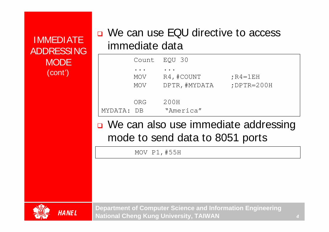
Example 5-5
Write a program to copy a block of 10 bytes of data from 35H to 60H
Solution:
MOV R0,#35H ;source pointerMOV R1,#60H ;destination pointerMOV R3,#10 ;counter
BACK: MOV A,@R0 ;get a byte from sourceMOV @R1,A ;copy it to destinationINC R0 ;increment source pointerINC R1 ;increment destination pointerDJNZ R3,BACK ;keep doing for ten bytes

Department of Computer Science and Information EngineeringNational Cheng Kung University, TAIWAN 16HANEL
ACCESSING MEMORY
Register Indirect
Addressing Mode(cont’)
R0 and R1 are the only registers that can be used for pointers in register indirect addressing modeSince R0 and R1 are 8 bits wide, their use is limited to access any information in the internal RAMWhether accessing externally connected RAM or on-chip ROM, we need 16-bit pointer
In such case, the DPTR register is used

Department of Computer Science and Information EngineeringNational Cheng Kung University, TAIWAN 17HANEL
ACCESSING MEMORY
Indexed Addressing Mode and
On-chip ROM Access
Indexed addressing mode is widely used in accessing data elements of look-up table entries located in the program ROMThe instruction used for this purpose is MOVC A,@A+DPTR
Use instruction MOVC, “C” means codeThe contents of A are added to the 16-bit register DPTR to form the 16-bit address of the needed data

Department of Computer Science and Information EngineeringNational Cheng Kung University, TAIWAN 18HANEL
ACCESSING MEMORY
Indexed Addressing
Mode and On-chip ROM
Access(cont’)
Example 5-6
In this program, assume that the word “USA” is burned into ROM locations starting at 200H. And that the program is burned into ROM locations starting at 0. Analyze how the program works and statewhere “USA” is stored after this program is run.
Solution:ORG 0000H ;burn into ROM starting at 0MOV DPTR,#200H ;DPTR=200H look-up table addrCLR A ;clear A(A=0)MOVC A,@A+DPTR ;get the char from code spaceMOV R0,A ;save it in R0INC DPTR ;DPTR=201 point to next charCLR A ;clear A(A=0)MOVC A,@A+DPTR ;get the next charMOV R1,A ;save it in R1INC DPTR ;DPTR=202 point to next charCLR A ;clear A(A=0)MOVC A,@A+DPTR ;get the next charMOV R2,A ;save it in R2
Here: SJMP HERE ;stay here;Data is burned into code space starting at 200H
ORG 200HMYDATA:DB “USA”
END ;end of program
DPTR=200H, A=0
U200
S201
A202
DPTR=200H, A=55H
DPTR=201H, A=55H
DPTR=201H, A=0
DPTR=201H, A=53H
DPTR=202H, A=53H
R0=55H
R1=53H
R2=41H

Department of Computer Science and Information EngineeringNational Cheng Kung University, TAIWAN 19HANEL
ACCESSING MEMORY
Look-up Table(cont’)
The look-up table allows access to elements of a frequently used table with minimum operations
Example 5-8Write a program to get the x value from P1 and send x2 to P2,
continuously
Solution:ORG 0MOV DPTR,#300H ;LOAD TABLE ADDRESSMOV A,#0FFH ;A=FFMOV P1,A ;CONFIGURE P1 INPUT PORT
BACK:MOV A,P1 ;GET XMOV A,@A+DPTR ;GET X SQAURE FROM TABLEMOV P2,A ;ISSUE IT TO P2SJMP BACK ;KEEP DOING IT
ORG 300HXSQR_TABLE:
DB 0,1,4,9,16,25,36,49,64,81END

Department of Computer Science and Information EngineeringNational Cheng Kung University, TAIWAN 20HANEL
ACCESSING MEMORY
Indexed Addressing Mode and
MOVX
In many applications, the size of program code does not leave any room to share the 64K-byte code space with data
The 8051 has another 64K bytes of memory space set aside exclusively for data storage
This data memory space is referred to as external memory and it is accessed only by the MOVX instruction
The 8051 has a total of 128K bytes of memory space
64K bytes of code and 64K bytes of dataThe data space cannot be shared between code and data

Department of Computer Science and Information EngineeringNational Cheng Kung University, TAIWAN 21HANEL
ACCESSING MEMORY
RAM Locations 30 – 7FH as Scratch Pad
In many applications we use RAM locations 30 – 7FH as scratch pad
We use R0 – R7 of bank 0 Leave addresses 8 – 1FH for stack usageIf we need more registers, we simply use RAM locations 30 – 7FH
Example 5-10Write a program to toggle P1 a total of 200 times. Use RAM location 32H to hold your counter value instead of registers R0 –R7
Solution:MOV P1,#55H ;P1=55HMOV 32H,#200 ;load counter value
;into RAM loc 32HLOP1: CPL P1 ;toggle P1
ACALL DELAYDJNZ 32H,LOP1 ;repeat 200 times

Department of Computer Science and Information EngineeringNational Cheng Kung University, TAIWAN 22HANEL
BIT ADDRESSES
Many microprocessors allow program to access registers and I/O ports in byte size only
However, in many applications we need to check a single bit
One unique and powerful feature of the 8051 is single-bit operation
Single-bit instructions allow the programmer to set, clear, move, and complement individual bits of a port, memory, or registerIt is registers, RAM, and I/O ports that need to be bit-addressable
ROM, holding program code for execution, is not bit-addressable
Department of Computer Science and Information EngineeringNational Cheng Kung University, TAIWAN 23HANEL
BIT ADDRESSES
Bit-Addressable
RAM
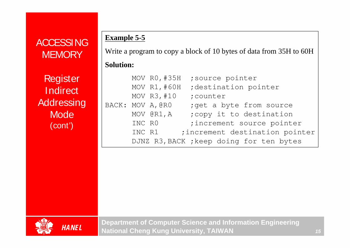
The bit-addressable RAM location are 20H to 2FH
These 16 bytes provide 128 bits of RAM bit-addressability, since 16 × 8 = 128
0 to 127 (in decimal) or 00 to 7FHThe first byte of internal RAM location 20H has bit address 0 to 7HThe last byte of 2FH has bit address 78H to 7FH
Internal RAM locations 20-2FH are both byte-addressable and bit-addressable
Bit address 00-7FH belong to RAM byte addresses 20-2FHBit address 80-F7H belong to SFR P0, P1, …

Department of Computer Science and Information EngineeringNational Cheng Kung University, TAIWAN 24HANEL
BIT ADDRESSES
Bit-Addressable
RAM(cont’)
Default register bank for R0-R70700
Bank 10F08
Bank 21710
Bank 31F18
000102030405060720
08090A0B0C0D0E0F21
101112131415161722
18191A1B1C1D1E1F23
202122232425262724
28292A2B2C2D2E2F25
303132333435363726
38393A3B3C3D3E3F27
404142434445464728
48494A4B4C4D4E4F29
50515253545556572A
58595A5B5C5D5E5F2B
60616263646566672C
68696A6B6C6D6E6F2D
70717273747576772E
78797A7B7C7D7E7F2F
General purpose RAM7F
30
Byte address
Bit-addressable locations

Department of Computer Science and Information EngineeringNational Cheng Kung University, TAIWAN 25HANEL
BIT ADDRESSES
Bit-Addressable
RAM(cont’)
Example 5-11Find out to which by each of the following bits belongs. Give the
address of the RAM byte in hex(a) SETB 42H, (b) CLR 67H, (c) CLR 0FH(d) SETB 28H, (e) CLR 12, (f) SETB 05
Solution:
(a) D2 of RAM location 28H
(b) D7 of RAM location 2CH
(c) D7 of RAM location 21H
(d) D0 of RAM location 25H
(e) D4 of RAM location 21H
(f) D5 of RAM location 20H
D0D1D2D3D4D5D6D7
000102030405060720
08090A0B0C0D0E0F21
101112131415161722
18191A1B1C1D1E1F23
202122232425262724
28292A2B2C2D2E2F25
303132333435363726
38393A3B3C3D3E3F27
404142434445464728
48494A4B4C4D4E4F29
50515253545556572A
58595A5B5C5D5E5F2B
60616263646566672C
68696A6B6C6D6E6F2D
70717273747576772E
78797A7B7C7D7E7F2F

Department of Computer Science and Information EngineeringNational Cheng Kung University, TAIWAN 26HANEL
BIT ADDRESSES
Bit-Addressable
RAM(cont’)
To avoid confusion regarding the addresses 00 – 7FH
The 128 bytes of RAM have the byte addresses of 00 – 7FH can be accessed in byte size using various addressing modes
Direct and register-indirect
The 16 bytes of RAM locations 20 – 2FH have bit address of 00 – 7FH
We can use only the single-bit instructions and these instructions use only direct addressing mode

Department of Computer Science and Information EngineeringNational Cheng Kung University, TAIWAN 27HANEL
BIT ADDRESSES
Bit-Addressable
RAM(cont’)
Instructions that are used for signal-bit operations are as following
Jump to target if bit = 1, clear bit (jump if bit, then clear)
JBC bit, targetJump to target if bit = 0 (jump if no bit)JNB bit, targetJump to target if bit = 1 (jump if bit)JB bit, targetComplement the bit (bit = NOT bit)CPL bitClear the bit (bit = 0)CLR bit
Set the bit (bit = 1)SETB bit
FunctionInstruction
Single-Bit Instructions

Department of Computer Science and Information EngineeringNational Cheng Kung University, TAIWAN 28HANEL
BIT ADDRESSES
I/O Port Bit Addresses
While all of the SFR registers are byte-addressable, some of them are also bit-addressable
The P0 – P3 are bit addressableWe can access either the entire 8 bits or any single bit of I/O ports P0, P1, P2, and P3 without altering the restWhen accessing a port in a single-bit manner, we use the syntax SETB X.Y
X is the port number P0, P1, P2, or P3Y is the desired bit number from 0 to 7 for data bits D0 to D7ex. SETB P1.5 sets bit 5 of port 1 high

Department of Computer Science and Information EngineeringNational Cheng Kung University, TAIWAN 29HANEL
BIT ADDRESSES
I/O Port Bit Addresses
(cont’)
Notice that when code such as SETB P1.0 is assembled, it becomes SETB 90H
The bit address for I/O portsP0 are 80H to 87H P1 are 90H to 97HP2 are A0H to A7HP3 are B0H to B7H
P2.7 (A7)P2.6P2.5P2.4P2.3P2.2P2.1P2.0 (A0)
P2
P3.7 (B7)P3.6P3.5P3.4P3.3P3.2P3.1P3.0 (B0)
P3
P1.7 (97)P1.6P1.5P1.4P1.3P1.2P1.1P1.0 (90)
P1
P0.7 (87)P0.6P0.5P0.4P0.3P0.2P0.1P0.0 (80)
P0
D7D6D5D4D3D2D1D0
Port Bit
Single-Bit Addressability of Ports

Department of Computer Science and Information EngineeringNational Cheng Kung University, TAIWAN 30HANEL
BIT ADDRESSES
I/O Port Bit Addresses
(cont’)
Special Function Register
Byte address
SFR RAM Address (Byte and Bit)
99
A0
A8
B0
B8
D0
E0
F0
FF
SBUF
P2
IE
P3
IP
PSW
ACC
B
not bit addressable
A7 A6 A5 A4 A3 A2 A1 A0
AF AE AD AC AB AA A9 A8
B7 B6 B5 B4 B3 B2 B1 B0
-- -- -- BC BB BA B9 B8
D7 D6 D5 D4 D3 D2 D1 D0
E7 E6 E5 E4 E3 E2 E1 E0
F7 F6 F5 F4 F3 F2 F1 F0
Bit address
DPLnot bit addressable82
SPnot bit addressable81
80
83
87
88
89
8A
8B
8C
8D
90
98
P0
DPH
PCON
TCON
TMOD
TL0
TL1
TH0
TH1
P1
SCON
87 86 85 84 83 82 81 80
not bit addressable
not bit addressable
8F 8E 8D 8C 8B 8A 89 88
not bit addressable
not bit addressable
not bit addressable
not bit addressable
not bit addressable
97 96 95 94 93 92 91 90
9F 9E 9D 9C 9B 9A 99 98
Bit addressByte address
Bit addresses 80 – F7H belong to SFR of P0, TCON, P1, SCON, P2, etc

Department of Computer Science and Information EngineeringNational Cheng Kung University, TAIWAN 31HANEL
BIT ADDRESSES
Registers Bit-
Addressability
Only registers A, B, PSW, IP, IE, ACC, SCON, and TCON are bit-addressable
While all I/O ports are bit-addressable
In PSW register, two bits are set aside for the selection of the register banks
Upon RESET, bank 0 is selectedWe can select any other banks using the bit-addressability of the PSW
P--OVRS0RS1--ACCY
18H - 1FH31110H - 17H20108H - 0FH11000H - 07H000AddressRegister BankRS0RS1

Department of Computer Science and Information EngineeringNational Cheng Kung University, TAIWAN 32HANEL
BIT ADDRESSES
Registers Bit-
Addressability (cont’)
Example 5-13Write a program to save the accumulator in R7 of bank 2.Solution:
CLR PSW.3SETB PSW.4MOV R7,A
Example 5-14While there are instructions such as JNC and JC to check the carry flag bit (CY), there are no such instructions for the overflow flag bit (OV). How would you write code to check OV?Solution:
JB PSW.2,TARGET ;jump if OV=1
P--OVRS0RS1--ACCY
Example 5-18While a program to save the status of bit P1.7 on RAM address bit 05.Solution:
MOV C,P1.7
MOV 05,C

Department of Computer Science and Information EngineeringNational Cheng Kung University, TAIWAN 33HANEL
BIT ADDRESSES
Registers Bit-
Addressability (cont’) Example 5-17
The status of bits P1.2 and P1.3 of I/O port P1 must be saved before they are changed. Write a program to save the status of P1.2 in bit location 06 and the status of P1.3 in bit location 07Solution:
CLR 06 ;clear bit addr. 06CLR 07 ;clear bit addr. 07JNB P1.2,OVER ;check P1.2, if 0 then jumpSETB 06 ;if P1.2=1,set bit 06 to 1
OVER: JNB P1.3,NEXT ;check P1.3, if 0 then jumpSETB 07 ;if P1.3=1,set bit 07 to 1
NEXT: ...
Example 5-15Write a program to see if the RAM location 37H contains an even value. If so, send it to P2. If not, make it even and then send it to P2.Solution:
MOV A,37H ;load RAM 37H into ACCJNB ACC.0,YES ;if D0 of ACC 0? If so jumpINC A ;it’s odd, make it even
YES: MOV P2,A ;send it to P2

Department of Computer Science and Information EngineeringNational Cheng Kung University, TAIWAN 34HANEL
BIT ADDRESSES
Using BIT
The BIT directive is a widely used directive to assign the bit-addressable I/O and RAM locations
Allow a program to assign the I/O or RAM bit at the beginning of the program, making it easier to modify them
Example 5-22A switch is connected to pin P1.7 and an LED to pin P2.0. Write a program to get the status of the switch and send it to the LED.
Solution:LED BIT P1.7 ;assign bitSW BIT P2.0 ;assign bitHERE: MOV C,SW ;get the bit from the port
MOV LED,C ;send the bit to the portSJMP HERE ;repeat forever

Department of Computer Science and Information EngineeringNational Cheng Kung University, TAIWAN 35HANEL
BIT ADDRESSES
Using BIT(cont’)
Example 5-20Assume that bit P2.3 is an input and represents the condition of an oven. If it goes high, it means that the oven is hot. Monitor the bit continuously. Whenever it goes high, send a high-to-low pulse to port P1.5 to turn on a buzzer.
Solution:OVEN_HOT BIT P2.3BUZZER BIT P1.5HERE: JNB OVEN_HOT,HERE ;keep monitoring
ACALL DELAYCPL BUZZER ;sound the buzzerACALL DELAYSJMP HERE

Department of Computer Science and Information EngineeringNational Cheng Kung University, TAIWAN 36HANEL
BIT ADDRESSES
Using EQU
Use the EQU to assign addressesDefined by names, like P1.7 or P2Defined by addresses, like 97H or 0A0H
Example 5-24A switch is connected to pin P1.7. Write a program to check the status of the switch and make the following decision.(a) If SW = 0, send “0” to P2(b) If SW = 1, send “1“ to P2
Solution:SW EQU P1.7MYDATA EQU P2HERE: MOV C,SW
JC OVERMOV MYDATA,#’0’SJMP HERE
OVER: MOV MYDATA,#’1’SJMP HEREEND
SW EQU 97HMYDATA EQU 0A0H

Department of Computer Science and Information EngineeringNational Cheng Kung University, TAIWAN 37HANEL
EXTRA 128 BYTE ON-CHIP RAM IN 8052
The 8052 has another 128 bytes of on-chip RAM with addresses 80 – FFH
It is often called upper memoryUse indirect addressing mode, which uses R0 and R1 registers as pointers with values of 80H or higher– MOV @R0, A and MOV @R1, A
The same address space assigned to the SFRs
Use direct addressing mode– MOV 90H, #55H is the same as MOV P1, #55H

Department of Computer Science and Information EngineeringNational Cheng Kung University, TAIWAN 38HANEL
EXTRA 128 BYTE ON-CHIP RAM IN 8052
(cont’)
Example 5-27Assume that the on-chip ROM has a message. Write a program to copy it from code space into the upper memory space starting at address 80H. Also, as you place a byte in upper RAM, give a copy to P0.
Solution:ORG 0MOV DPTR,#MYDATAMOV R1,#80H ;access the upper memory
B1: CLR AMOVC A,@A+DPTR ;copy from code ROMMOV @R1,A ;store in upper memoryMOV P0,A ;give a copy to P0JZ EXIT ;exit if last byteINC DPTR ;increment DPTRINC R1 ;increment R1SJMP B1 ;repeat until last byte
EXIT: SJMP $ ;stay here when finished;---------------
ORG 300HMYDATA: DB “The Promise of World Peace”,0
END