
2_0 BJT AC 1
51
-
Upload
arum-setyaningtyas -
Category
Documents
-
view
229 -
download
0
Transcript of 2_0 BJT AC 1

7/23/2019 2_0 BJT AC 1
http://slidepdf.com/reader/full/20-bjt-ac-1 1/51

7/23/2019 2_0 BJT AC 1
http://slidepdf.com/reader/full/20-bjt-ac-1 2/51
Pemodelan AC dari suatu rangkaian diperoleh dengan :
1. Hilangkan semua sumber DC, ganti dengan short circuit
2. Ganti kapasitor dengan short circuit
3. Gambar rangkaian pengganti
Remember pada rangkaian RC seri dg sumber V, maka arus
yang mengalir pada kapasitor (Xc) adalah i=v/R2+Xc2,
sehingga bila Xc<< R, maka arus akan mengalir (sepertiasumsi short circuit
Pada dasarnya transitor bukan saja digunakan untuk proses input yang linier
saja (DC), namun perlu (punya kemampuan) analisis (proses) sinyal non-
linier (AC) kebanyakan bagian dari transmitter/reciever dari suatu pancaran
gelombang terdiri dari komponen transistor
Berarti harus ada piranti tambahan (kapasitor) yang akan meloloskan
sinyal AC (bypass/coupling capacitor)
Sedangkan untuk melihat sinyal keluaran dari transitor digunakan
beberapa cara dengan Common Emitter (CE), Common Collector
(CC) dan Common Base (CB)
ingat pelajaran tentang RLC, maka masalah impedansi adalah halpenting untuk dianalisis juga, penguatan yang dapat dilakukan oleh
transistor dan berbagai permasalahan bila transistor di-cascade
7/23/2019 2_0 BJT AC 1
http://slidepdf.com/reader/full/20-bjt-ac-1 3/51
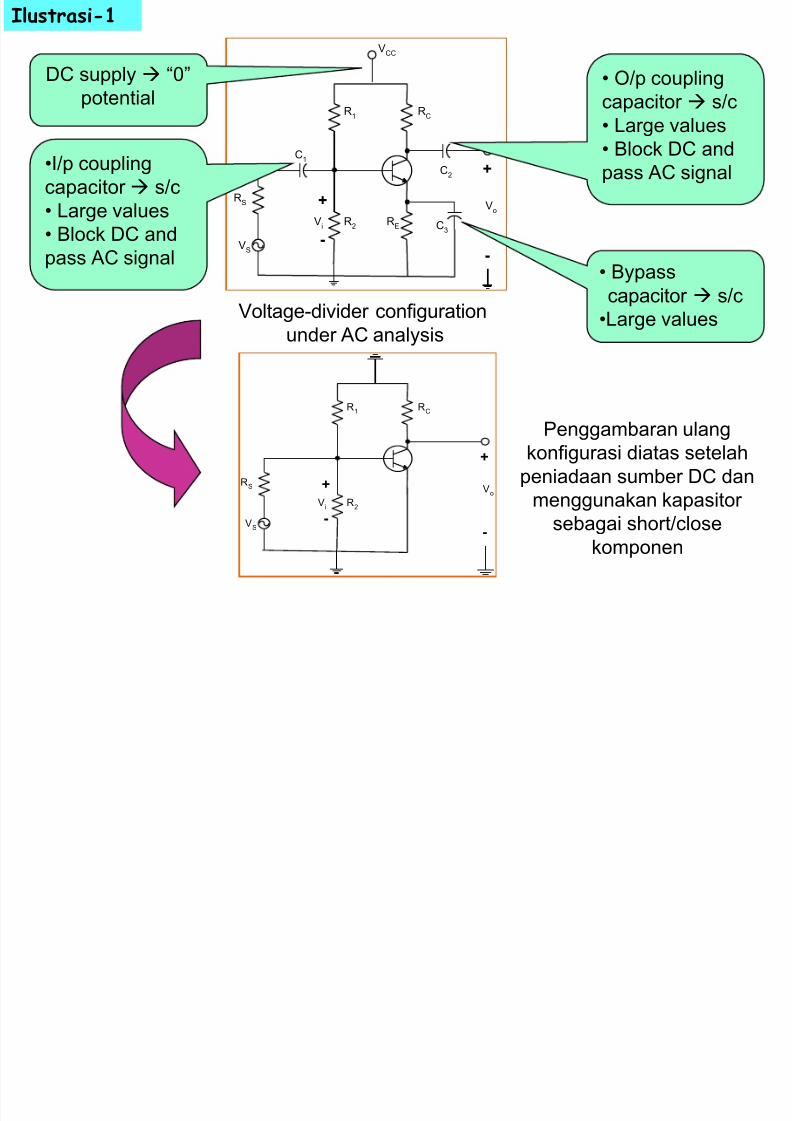
VS
VCC
C1
C2
C3
+
-
Vo
RS
Vi
+
-
RE
RC
R1
R2
VS
+
-
Vo
RS
Vi
+
-
RC
R1
R2
•I/p coupling
capacitor s/c
• Large values
• Block DC and
pass AC signal
• Bypasscapacitor s/c
•Large values
DC supply “0”
potential
Voltage-divider configuration
under AC analysis
Penggambaran ulang
konfigurasi diatas setelah
peniadaan sumber DC dan
menggunakan kapasitor
sebagai short/close
komponen
• O/p coupling
capacitor s/c
• Large values
• Block DC and
pass AC signal
Ilustrasi-1

7/23/2019 2_0 BJT AC 1
http://slidepdf.com/reader/full/20-bjt-ac-1 4/51
VS
RS
R2R1R
c
Transistor small-
signal ac
equivalent cct
Vo
Zi
Ii
Zo
Io
Vi
++
- -
B
E
C
Redrawn for small-signal AC analysis
Modeling of BJ T begin
HERE!
VS
+
-
VoRS
Vi
+
-
RCR1
R2
Ilustrasi-2 lanjutan
7/23/2019 2_0 BJT AC 1
http://slidepdf.com/reader/full/20-bjt-ac-1 5/51
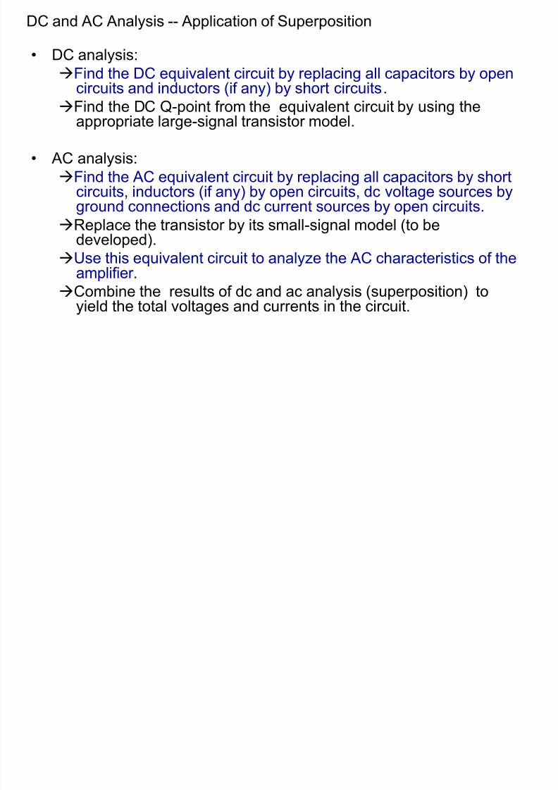
DC and AC Analysis -- Application of Superposition
• DC analysis:
Find the DC equivalent circuit by replacing all capacitors by opencircuits and inductors (if any) by short circuits.
Find the DC Q-point from the equivalent circuit by using theappropriate large-signal transistor model.
• AC analysis:
Find the AC equivalent circuit by replacing all capacitors by short
circuits, inductors (if any) by open circuits, dc voltage sources byground connections and dc current sources by open circuits.
Replace the transistor by its small-signal model (to bedeveloped).
Use this equivalent circuit to analyze the AC characteristics of theamplifier.
Combine the results of dc and ac analysis (superposition) toyield the total voltages and currents in the circuit.

7/23/2019 2_0 BJT AC 1
http://slidepdf.com/reader/full/20-bjt-ac-1 6/51
Lihat Malvino (3rd edition) halaman 177 gambar 7-4/Slide selanjutnya. Kalau
pada analisa DC (kuliah2 sebelum ini) pad penggambaran garis beban
terdapat nilai Q yang bervariasi pada kurva Ic vs Vcc berupa garis lurus saja
Namun pada gambar 7-4 d tsb digambarkan untuk yang beroperasi disekitar
Q dg bentuk sinyal sinus luaran pada VBE akan bervariasi berupa sinus juga (ingat pada kuliah sebelumnya kita hanya memiliki harga pasti (konstan)
dari VBE
Hal tersebut akan terjadi bila sinyal yang masuk ke transistor adalah AC,
sehingga berdasar gambar ketiga diatas, maka diode tergantikan oleh
tahanan di emiter (r’e)
+VBE
+VBE
r’e
IC IC
Pendekatan Diode untuk
Analisa DC
Pendekatan Diode untuk
Analisa AC
Tahanan bulk
dari emiter
7/23/2019 2_0 BJT AC 1
http://slidepdf.com/reader/full/20-bjt-ac-1 7/51
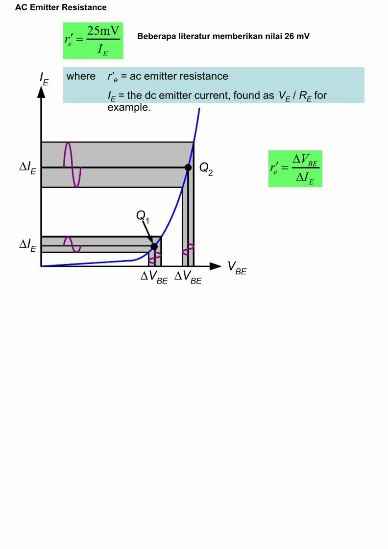
where r’ e = ac emitter resistance
I E = the dc emitter current, found as V E / R E for example.
25mVe
E
r I
AC Emitter Resistance
BE e
E
V r
I
I E
V BE V BE V BE
Q2
I E
I E
Q1
Beberapa literatur memberikan nilai 26 mV
7/23/2019 2_0 BJT AC 1
http://slidepdf.com/reader/full/20-bjt-ac-1 8/51
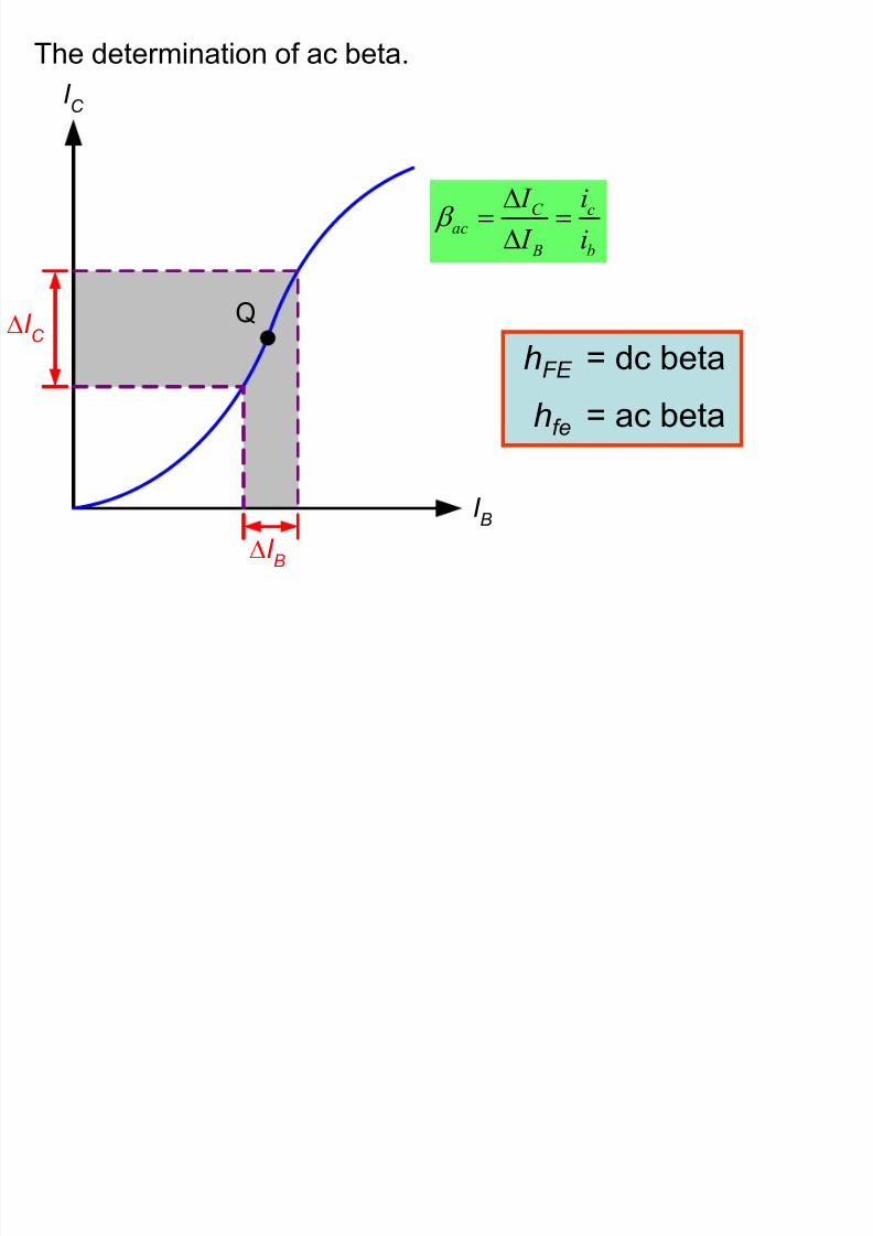
The determination of ac beta.
I B
I C
Q
I B
I C
C cac
B b
I i
I i
hFE = dc beta
hfe = ac beta

7/23/2019 2_0 BJT AC 1
http://slidepdf.com/reader/full/20-bjt-ac-1 9/51
AC Model of A BJT
npn pnp
B C
E
B C
E
b
c
e
i b
i c
= aci b
r' e

7/23/2019 2_0 BJT AC 1
http://slidepdf.com/reader/full/20-bjt-ac-1 10/51
Standarisasi notasi AC dan
DC
IE, IC, IB ie, ic, ib
VE, VC, VB ve,vc,vb
VBE, VCE, VCB vbe, vce, vcb
dc, , r’e hFE, hfe, hrb
DC AC

7/23/2019 2_0 BJT AC 1
http://slidepdf.com/reader/full/20-bjt-ac-1 11/51
Fig 9.12a Example 9.2. Analisa Output Untuk
Sinyal AC dan DC (Cshort)
V CC
Q1
R E
R C
R 1
R 2
R L
C C 1
C C 2
C B
GND
Q1
R E
R C
R 1
R 2
R L
7/23/2019 2_0 BJT AC 1
http://slidepdf.com/reader/full/20-bjt-ac-1 12/51
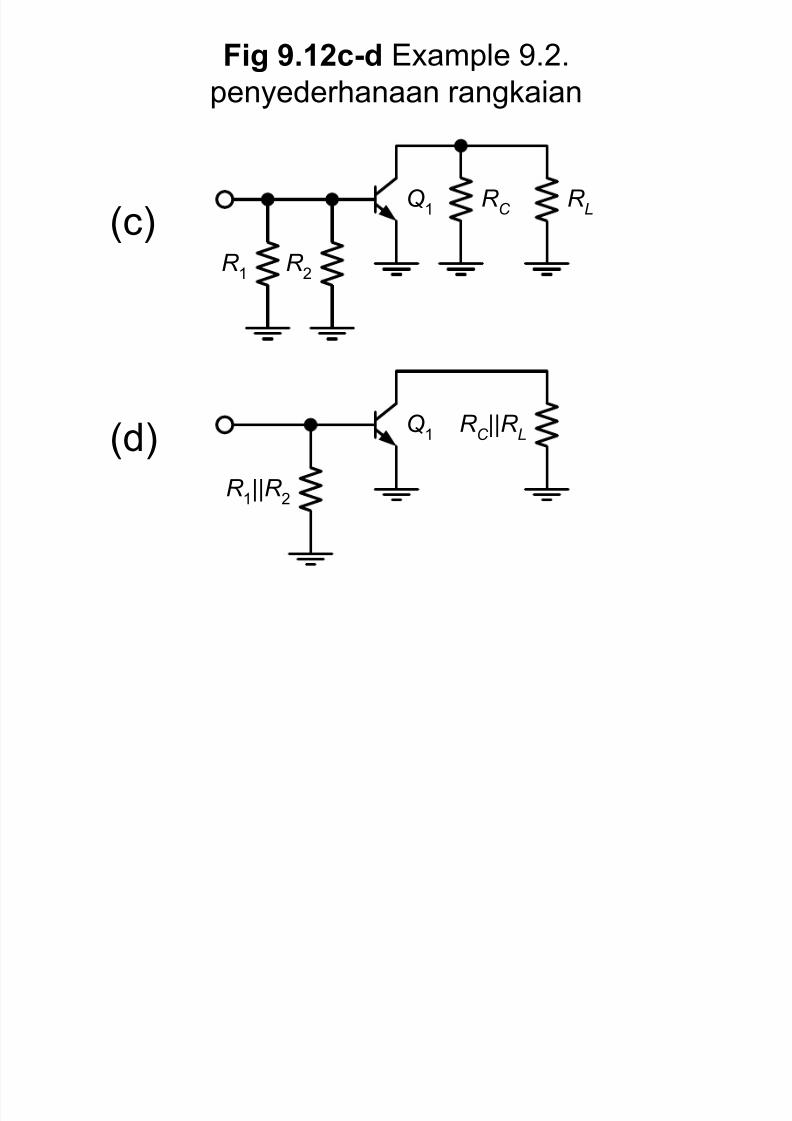
Fig 9.12c-d Example 9.2.
penyederhanaan rangkaian
Q1
R C
R 1
R 2
R L
Q1
R 1||R
2
R C ||R L
(c)
(d)

7/23/2019 2_0 BJT AC 1
http://slidepdf.com/reader/full/20-bjt-ac-1 13/51
Voltage Gain DC of CE
Lcccc
Lccout
R Rr wherer i
R Riv
..
)(
out
in
c C C
ve e e
v i r r A
v i r r
Q1
R 1||R
2
R C ||R
Li b
i c
= i b
r' e
v in
v out
Q1
R 1||R
2
R C ||R
L
in e ev i r
25mVe
E
r I
“-” fase out berbeda 180’ input

7/23/2019 2_0 BJT AC 1
http://slidepdf.com/reader/full/20-bjt-ac-1 14/51
V CC
Q1
R E
R C
R 1
R 2
R L
C C 1
C C 2
C B
GND
Q1
R E
R C
R 1
R 2
R L
Q1
R C
R 1 R 2
R L
Q1
R 1||R
2
R C ||R
L
Q1
R 1||R 2
R C ||R
Li b
i c
= i b
r' e
v in
v out
Q1
R 1||R 2
R C ||R
L
out
in
c C C v
e e e
v i r r A
v i r r
out
where
c C L
c C C C L
v i R R
i r r R R
in e ev i r
1) AC circuit
2) AC Circuit
2.a)
2.b)
3) AC Circuit
3.a)
3.b)
Voltage Gain CE
Summary

7/23/2019 2_0 BJT AC 1
http://slidepdf.com/reader/full/20-bjt-ac-1 15/51
Perhatikan Malvino p.173 gbr. 9.2.b
-vbe+(ic/).rb+ie(r’e+re)0 didapat ie
/' rBer rE
vbbie
vc=ie.rC
ve=ie.rE
vb=ie(r’e+rE)
Penguat Tegangan ACCara 1 A=(vc/vb)
Cara 2 A=(rC/rE+r’e)
Singkatnya
Analias Dc untuk
mendapatkan IE
Analias AC untuk
liat gain dan bentuk
sinyal output
Penghubung AC &
DC melalui,
r’e=25mV/IE
C t h 1 ( t d b )

7/23/2019 2_0 BJT AC 1
http://slidepdf.com/reader/full/20-bjt-ac-1 16/51
+ 30 V
100
R C
10kR 1
20 k
R 2
10k
R L10 k
~
Vbb
10k
10k
20k 10k
10 k
~100
r’e 5k
~100
Contoh-1 (penguat dg common base)+ 30 V
10,1 k
R C 10k20 k
10k
Untuk analisa
DC, maka
semua kapasitor
open shg.
Menjadi gbr. (2)
Untuk dapat r’e diperlukan IB
(DC), maka dg voltage
devider Diperoleh IB, 10 V,
shg dg asumsi VBE≈0, maka
VE=10 V dan IE=10/10,1Katau sekitar 1 mA, shg
didapat r’e=(25 mV/IE) atausama dengan 25 Ω
Seri antara 100 Ω
dan 10 KΩ
1
2
3Untuk analisa AC, maka
kapasitor gbr (1) semua
short dan VCC = 0 /' rBer rE
vbbie
4
vc=ie.rC
ve=ie.rE
vb=ie(r’e+rE)
Cara 1 A=(vc/vb) Cara 2
A=(rC/rE+r’e)

7/23/2019 2_0 BJT AC 1
http://slidepdf.com/reader/full/20-bjt-ac-1 17/51
Vi
Vo
RC
C1
C2
VCC
R1
RER2
R1
RER2
Redrawn the input side of the network
Thevenin
VCC
R1
R2RTH
Determining RTH
R1
R2VCC VR2
+
-
ETH
+
-
Determining ETH
RTH
RE
Inserting the Theveninequivalent cct.
ETH IE
IB VBE
+
-
21TH R R R
21
CC2
2R TH
R R
VR VE
0R IVR IE EEBETHBTH
givesI1βI Subtitute
BE
ETH
BETH
B
R 1R
VEI
1 2 3
4 5
C t h 1 (C E itt ) T f th b i it t it Th i

7/23/2019 2_0 BJT AC 1
http://slidepdf.com/reader/full/20-bjt-ac-1 18/51
+20 V
hFE
= 200
R E
2.2k
R C
12k
R 1
150k
R 2
20k
R L
50k
Contoh-1 (Common Emitter) Transform the base circuit to its Theveninequivalent.
2
1 2
1 2
20k Ω20V
170k Ω
2.353V
20k Ω 150kΩ
17.65k Ω
th CC
th
RV V
R R
R R R
2.353V 0.7V
( 1) 17.65k Ω 201 2.2kΩ
3.595μA
th BE B
th FE E
V V I
R h R
200 3.595μA 718.9μA
1 201 3.595μA 722.5μA
C FE B
E FE B
I h I
I h I
20V 718.9μA 12kΩ 722.5μA 2.2kΩ
9.784V active
CE CC C C E E V V I R I R
25mV 25mV34.6Ω
722.5μA
12k Ω 50kΩ 9.677kΩ
e
E
C C L
r I
r R R
9.677k Ω279.7
34.6Ω
C v
e
r A
r
1
)
2)
3)
4)
5)
F 1 E l 4 (1)

7/23/2019 2_0 BJT AC 1
http://slidepdf.com/reader/full/20-bjt-ac-1 19/51
Fig 9.13 Example 9.4. (1)
+20 V
hFE
= 200
R E 2.2k
R C
12kR
1
150k
R 220k
R L
50k
Transform the base circuit to itsThevenin equivalent.
2
1 2
1 2
20k Ω20V
170k Ω
2.353V
20k Ω 150kΩ
17.65k Ω
th CC
th
RV V
R R
R R R
2.353V 0.7V
( 1) 17.65k Ω 201 2.2kΩ
3.595μA
th BE B
th FE E
V V I
R h R

7/23/2019 2_0 BJT AC 1
http://slidepdf.com/reader/full/20-bjt-ac-1 20/51
Fig 9.13 Example 9.4. (2)
+20 V
hFE
= 200
R E
2.2k
R C
12k
R 1
150k
R 220k
R L
50k
200 3.595μA 718.9μA
1 201 3.595μA 722.5μA
C FE B
E FE B
I h I
I h I
20V 718.9μA 12kΩ 722.5μA 2.2kΩ
9.784V active
CE CC C C E E V V I R I R
25mV 25mV34.6Ω
722.5μA
12k Ω 50kΩ 9.677kΩ
e
E
C C L
r I
r R R
9.677k Ω279.7
34.6Ω
C v
e
r A
r

7/23/2019 2_0 BJT AC 1
http://slidepdf.com/reader/full/20-bjt-ac-1 21/51
Fig 9.14 Example 9.5. (1)
Transform the base circuit to itsThevenin equivalent.
2
1 2
1 2
4.7k Ω10V
22.7k Ω
2.070V
4.7k Ω 18kΩ
3.727k Ω
th CC
th
RV V
R R
R R R
2.070V 0.7V
( 1) 3.727k Ω 31 1.2kΩ
33.49μA
th BE B
th FE E
V V I
R h R
+10 V
hFE
= 30
hfe
= 200
R E
1.2k
R C
1.5kR 1
18k
R 24.7k
R L
5k

7/23/2019 2_0 BJT AC 1
http://slidepdf.com/reader/full/20-bjt-ac-1 22/51
Fig 9.14 Example 9.5. (2)
30 33.49μA 1.005mA
1 31 33.49μA 1.038mAC FE B
E FE B
I h I I h I
10V 1.005mA 1.5k Ω 1.038mA 1.2kΩ
7.247V active
CE CC C C E E V V I R I R
25mV 25mV24.08Ω
1.038mA
1.5k Ω 5kΩ 1.154kΩ
e
E
C C L
r I
r R R
1.154k Ω47.91
24.08Ω
C v
e
r A
r
+10 V
hFE
= 30
hfe
= 200
R E
1.2k
R C
1.5kR 1
18k
R 24.7k
R L
5k

7/23/2019 2_0 BJT AC 1
http://slidepdf.com/reader/full/20-bjt-ac-1 23/51

7/23/2019 2_0 BJT AC 1
http://slidepdf.com/reader/full/20-bjt-ac-1 24/51
Power Gain
p i v A A A
Example 9.7 The amplifier shown in Fig. 9.5 has
values of Av = 45.3 and Ai = 20. Determine thepower gain ( A p) of the amplifier and the outputpower when Pin = 80 mW.
20 45.3 906 p i v A A A
out in 906 80μW 72.48mW p P A P
7/23/2019 2_0 BJT AC 1
http://slidepdf.com/reader/full/20-bjt-ac-1 25/51
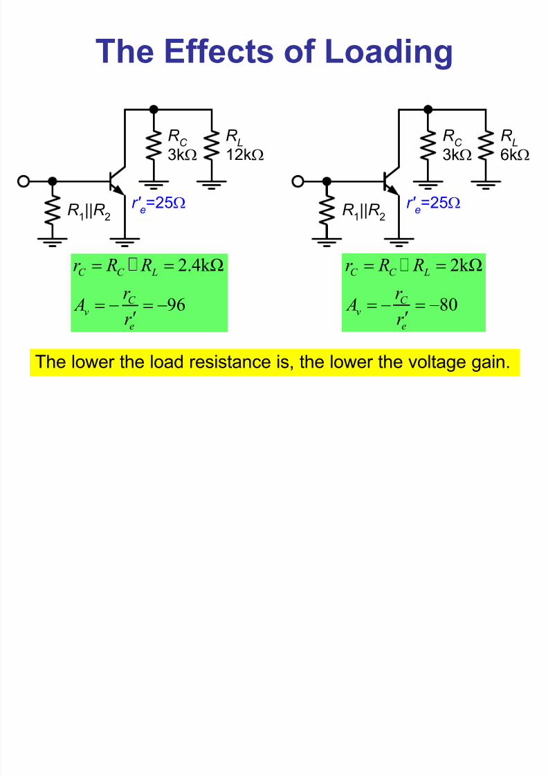
The Effects of Loading
The lower the load resistance is, the lower the voltage gain.
2.4k Ω
96
C C L
C v
e
r R R
r A
r
2k Ω
80
C C L
C v
e
r R R
r Ar
R C
3k
R L
6k
R 1||R
2r' e=25
R C
3k
R L
12k
R 1||R
2r' e=25
7/23/2019 2_0 BJT AC 1
http://slidepdf.com/reader/full/20-bjt-ac-1 26/51
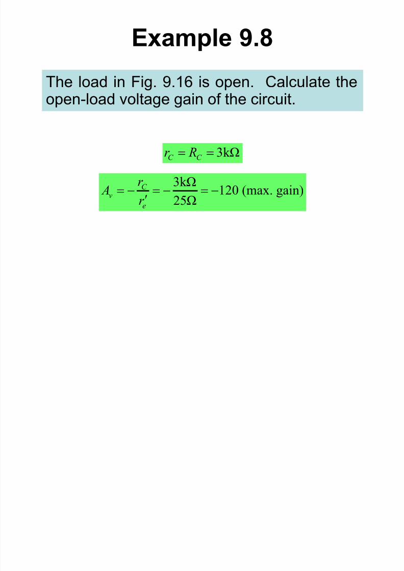
Example 9.8
The load in Fig. 9.16 is open. Calculate theopen-load voltage gain of the circuit.
3k ΩC C r R
3k Ω120 (max. gain)
25Ω
C v
e
r A
r
7/23/2019 2_0 BJT AC 1
http://slidepdf.com/reader/full/20-bjt-ac-1 27/51
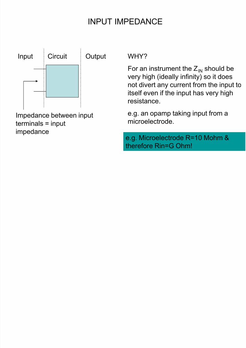
INPUT IMPEDANCE
WHY?
For an instrument the ZIN should be
very high (ideally infinity) so it does
not divert any current from the input toitself even if the input has very high
resistance.
e.g. an opamp taking input from a
microelectrode.
Input Circuit Output
Impedance between input
terminals = input
impedancee.g. Microelectrode R=10 Mohm &
therefore Rin=G Ohm!
7/23/2019 2_0 BJT AC 1
http://slidepdf.com/reader/full/20-bjt-ac-1 28/51
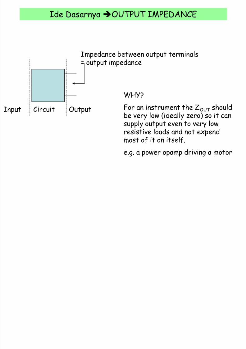
Ide DasarnyaOUTPUT IMPEDANCE
Input Circuit Output
Impedance between output terminals= output impedance
WHY?
For an instrument the ZOUT shouldbe very low (ideally zero) so it cansupply output even to very low
resistive loads and not expendmost of it on itself.
e.g. a power opamp driving a motor
A common-emitter (CE) amplifie

7/23/2019 2_0 BJT AC 1
http://slidepdf.com/reader/full/20-bjt-ac-1 29/51
A common emitter (CE) amplifie
capacitors are used for coupling ac without disturbing dc levels
• Vout is biased at middle of V+
• AC Gain: G = - Rc / RE
0
(V+)/20.1
(V+)/2 + G*0.1
(V+)/2 - G*0.1-0.1

7/23/2019 2_0 BJT AC 1
http://slidepdf.com/reader/full/20-bjt-ac-1 30/51
Phase Relationship
The phase relationship between input and output is 180 degrees. The negative
sign used in the voltage gain formulas indicates the inversion.
Ilustrasi-1
7/23/2019 2_0 BJT AC 1
http://slidepdf.com/reader/full/20-bjt-ac-1 31/51
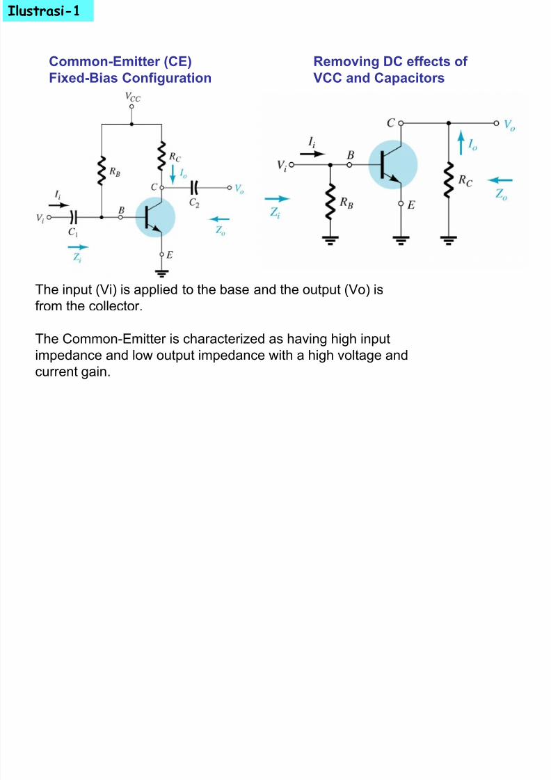
Ilustrasi 1
The input (Vi) is applied to the base and the output (Vo) isfrom the collector.
The Common-Emitter is characterized as having high input
impedance and low output impedance with a high voltage and
current gain.
Removing DC effects of
VCC and Capacitors
Common-Emitter (CE)
Fixed-Bias Configuration
f CIlustrasi-2
7/23/2019 2_0 BJT AC 1
http://slidepdf.com/reader/full/20-bjt-ac-1 32/51
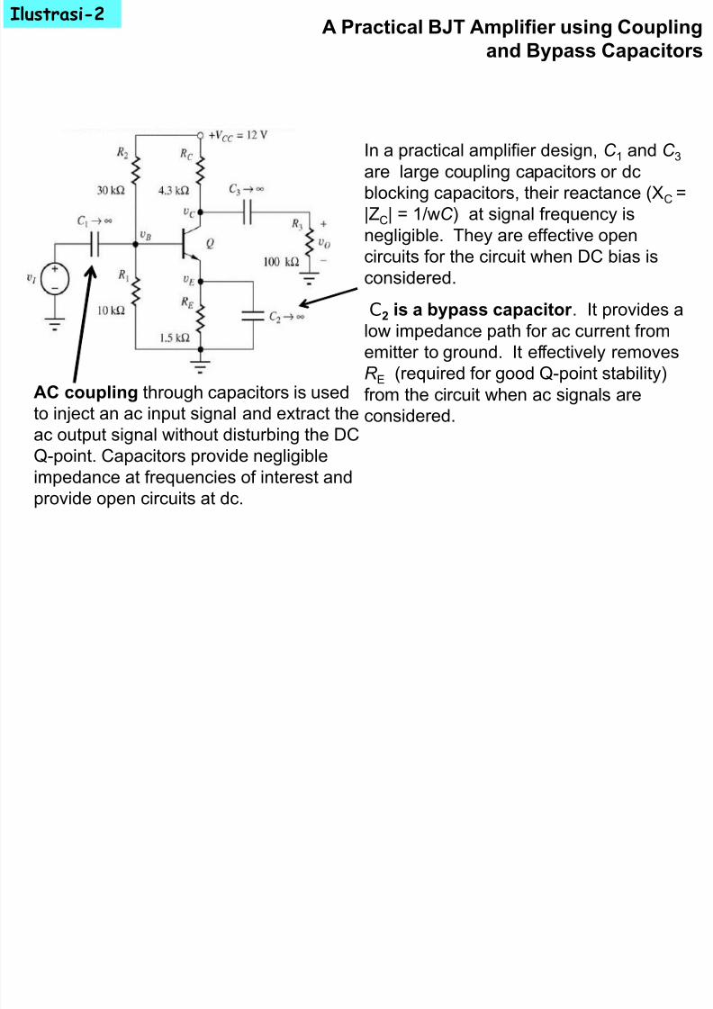
A Practical BJT Amplifier using Coupling
and Bypass Capacitors
AC coupling through capacitors is used
to inject an ac input signal and extract the
ac output signal without disturbing the DC
Q-point. Capacitors provide negligible
impedance at frequencies of interest and
provide open circuits at dc.
In a practical amplifier design, C 1 and C 3
are large coupling capacitors or dc
blocking capacitors, their reactance (XC =
|ZC| = 1/wC ) at signal frequency is
negligible. They are effective open
circuits for the circuit when DC bias isconsidered.
C2 is a bypass capacitor . It provides a
low impedance path for ac current from
emitter to ground. It effectively removes
R E (required for good Q-point stability)from the circuit when ac signals are
considered.
Ilustrasi 2

7/23/2019 2_0 BJT AC 1
http://slidepdf.com/reader/full/20-bjt-ac-1 33/51
Calculating Amp.
Input Impedance
in 1 2 in(base) Z R R Z
Z in(base)
Z in
R 1
R 2
Biasing circuit
V CC
IN(base)DC: 1 FE E
FE E
R h R
h R
in(base)AC: 1 fe e
fe e
Z h r
h r
Rin=(dc+1 )Re
7/23/2019 2_0 BJT AC 1
http://slidepdf.com/reader/full/20-bjt-ac-1 34/51
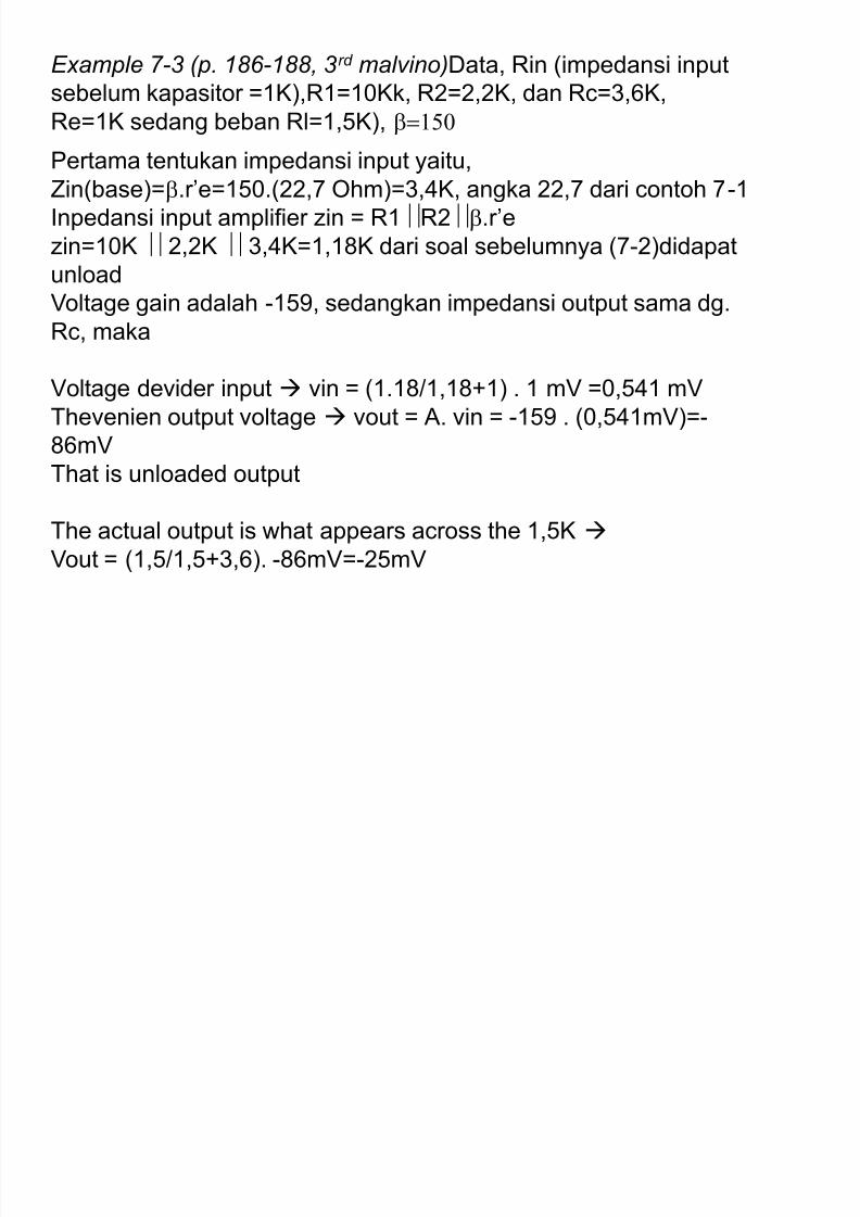
Example 7-3 (p. 186-188, 3rd malvino)Data, Rin (impedansi input
sebelum kapasitor =1K),R1=10Kk, R2=2,2K, dan Rc=3,6K,
Re=1K sedang beban Rl=1,5K), 150
Pertama tentukan impedansi input yaitu,Zin(base)=.r’e=150.(22,7 Ohm)=3,4K, angka 22,7 dari contoh 7-1
Inpedansi input amplifier zin = R1R2.r’e
zin=10K 2,2K 3,4K=1,18K dari soal sebelumnya (7-2)didapat
unload
Voltage gain adalah -159, sedangkan impedansi output sama dg.Rc, maka
Voltage devider input vin = (1.18/1,18+1) . 1 mV =0,541 mV
Thevenien output voltage vout = A. vin = -159 . (0,541mV)=-
86mVThat is unloaded output
The actual output is what appears across the 1,5K
Vout = (1,5/1,5+3,6). -86mV=-25mV

7/23/2019 2_0 BJT AC 1
http://slidepdf.com/reader/full/20-bjt-ac-1 35/51
Fig 9.17 Example 9.9.
in(base)
200 24Ω 4.8kΩ fe e
Z h r
in 1 2 in(base)
18k Ω 4.7kΩ 4.8kΩ
2.1k Ω
Z R R Z
+10 V
hFE = 30hfe
= 200
R E
1.2k
R C
1.5kR 1
18k
R 2
4.7k
R L5k
Z in(base)
Z in
Q1
R 2
4.7k
R 1
18k
R C
1.5k
R L
5k
r' e
= 24
hfe = 200
Z in(base)
Z in

7/23/2019 2_0 BJT AC 1
http://slidepdf.com/reader/full/20-bjt-ac-1 36/51
Calculating the Value of Ai
out
in
i
i A
i c
fe
b
ih
i
out out
out
c L C c C L
c C
L
v i R R i r i R
i r i
R
in in in in(base)
in(base)
in
in in
1
b
b fe eb
v i Z i Z
i h r i Z i
Z Z
in
in(base)
C i fe
L
Z r A h
Z R
Q1
R C
R 1
R 2
R L
i c i b
Z in(base)
i out
v out
i in
v in
Z in

7/23/2019 2_0 BJT AC 1
http://slidepdf.com/reader/full/20-bjt-ac-1 37/51
Example 9.10
Calculate the value of Ai for the circuit shown in Fig. 9.17.
in(base) 200 24Ω 4.8kΩ fe e Z h r
in 1 2 in(base) 2.1k Ω Z R R Z
1.15k ΩC C Lr R R
in
in(base)
2.1k Ω 1.15kΩ200
4.8k Ω 5kΩ
20.2
C i fe
L
Z r A h Z R
Q1
R 2
4.7k
R 1
18k
R C
1.5k
R L
5k
r' e
= 24
hfe
= 200
Z in(base)
Z in

7/23/2019 2_0 BJT AC 1
http://slidepdf.com/reader/full/20-bjt-ac-1 38/51
Multistage Amp.
Gain Calculations
1 2 3vT v v v A A A A
1 2 3iT i i i A A A A
pT vT iT A A A
Procedure:
1. Do dc analysis
2. Findr’ e for each stage
3. Find r C for each stage
4. Using r’ e and r C to find Av
for each stage Input impedance of next stage is the load of current stage.
(Z in of next stage is RL of current stage)

7/23/2019 2_0 BJT AC 1
http://slidepdf.com/reader/full/20-bjt-ac-1 39/51
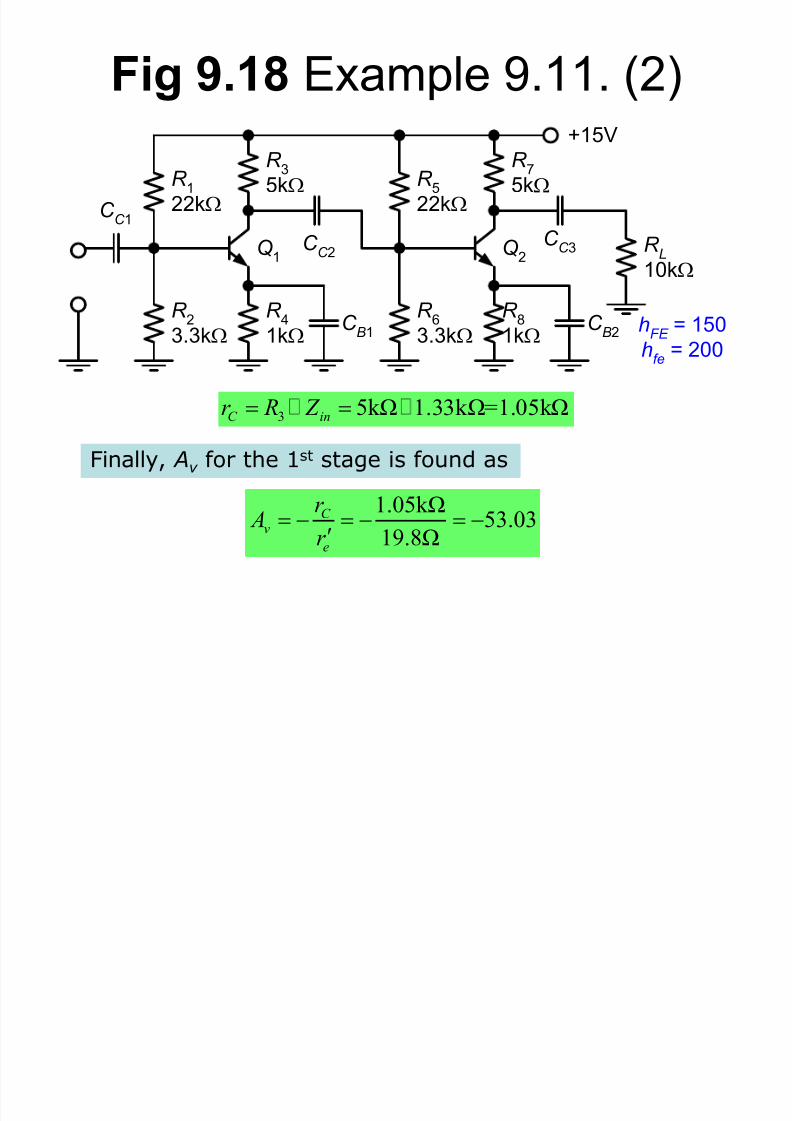
Fig 9.18 Example 9.11. (1)
( ) 1 201 17.4 3.497k Ωin base fe e Z h r
Determine Av of the 1st
stage. Assume that r’ e for the 1st stage is 19.8 and r’ e for the 2nd stage isfound to be 17.4 . Forthe 2nd stage, hfe is 200. 5 6 ( ) 1.329k Ωin in base Z R R Z
The input impedance of the 2
nd
stage:
+15V
C C 1
C C 2
C C 3
R 1
22k
R 2
3.3k
R 4
1kC
B1
R 8
1kC
B2
R 3
5k R 5
15k
R 6
2.5k
R 7
5k
R L
10kQ
1Q
2
hFE
= 150
hfe
= 200
7/23/2019 2_0 BJT AC 1
http://slidepdf.com/reader/full/20-bjt-ac-1 40/51
Fig 9.18 Example 9.11. (2)
+15V
C C 1
C C 2
C C 3
R 1
22k
R 2
3.3k
R 4
1kC
B1
R 8
1kC
B2
R 3
5k R 5
22k
R 6
3.3k
R 7
5k
R L
10kQ
1Q
2
hFE
= 150
hfe
= 200
35k Ω 1.33kΩ=1.05kΩ
C inr R Z
Finally, Av for the 1st stage is found as 1.05k Ω
53.0319.8Ω
C v
e
r A
r

7/23/2019 2_0 BJT AC 1
http://slidepdf.com/reader/full/20-bjt-ac-1 41/51
Example 9.12. (1)
Determine the value of AvT for the amplifier in Figure9.18. r C for the 2nd stage can be found as
7 3.33k ΩC Lr R R
3.33k Ω
191.3817.4Ω
C
ve
r
A r
Av for the 2nd stage is found as
3
1 2 53.03 191.38 10.15 10vT v v A A A
Fi 9 19 Th d CE lifi d

7/23/2019 2_0 BJT AC 1
http://slidepdf.com/reader/full/20-bjt-ac-1 42/51
Fig 9.19 The swamped CE amplifier and
its ac equivalent ckt.
Swamped amplifier is anamplifier that uses a partiallybypassed emitter resistance toincrease ac emitter resistance.
Also referred to as a gain-stabilized amplifier. R
C
r E
R E
C B
R 1
R 2
C 1
C 2 R
L
+V CC
Q1
r E
Q1
r C
R 1//R
2

7/23/2019 2_0 BJT AC 1
http://slidepdf.com/reader/full/20-bjt-ac-1 43/51
Distortion (Bagian dari efek Negatip Swamp)
• The location of the point Q (size of the dc source on input) may
cause an operating point to lie outside of the active range.
Driven to saturationDriven into Cutoff
7/23/2019 2_0 BJT AC 1
http://slidepdf.com/reader/full/20-bjt-ac-1 44/51
Av of Swamped Amp.
C v
e E
r A
r r
r E
Q1
r C
R 1//R
2
r C
R 1//R
2
r E
r' e
i b
i c
= ac i b
Q1
v in
v out
out c C
v
in e e E
v i r A
v i r r

7/23/2019 2_0 BJT AC 1
http://slidepdf.com/reader/full/20-bjt-ac-1 45/51
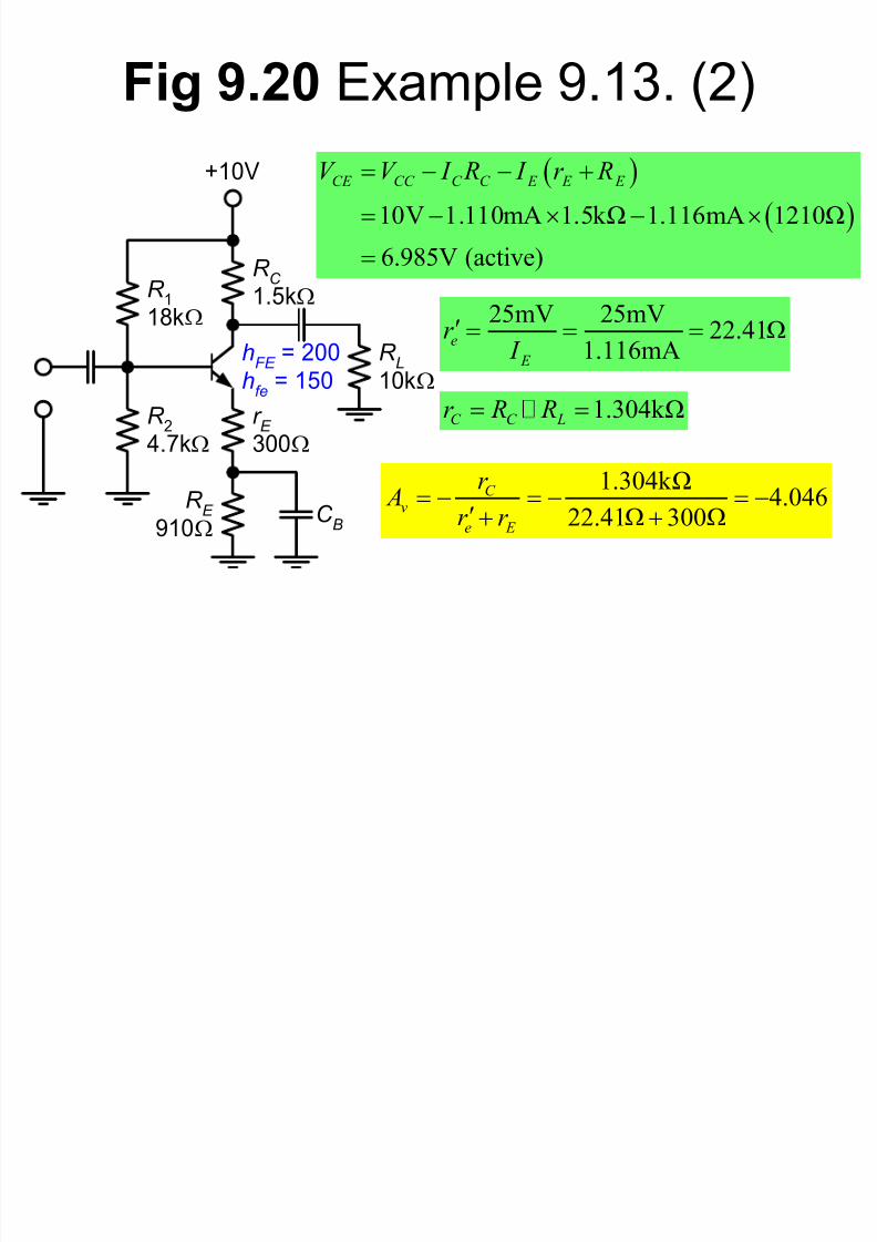
Fig 9.20 Example 9.13. (1)
R C
1.5k
r E
300
R E 910
C B
R 1
18k
R 2
4.7k
R L
10k
+10V
hFE
= 200hfe
= 150
2
1 2
1 2
4.7k Ω10V 2.070V
22.7k Ω
18k Ω 4.7kΩ 3.727kΩ
th CC
th
RV V
R R
R R R
1
2.070V 0.7V
3.727k Ω 201 1210Ω
5.550μA
200 5.550μA
1.110mA
1 201 5.550μA
1.116mA
th BE B
th FE E E
C FE B
E FE B
V V
I R h r R
I h I
I h I
7/23/2019 2_0 BJT AC 1
http://slidepdf.com/reader/full/20-bjt-ac-1 46/51
Fig 9.20 Example 9.13. (2)
R C
1.5k
r E
300
R E
910C
B
R 1
18k
R 2
4.7k
R L
10k
+10V
hFE
= 200hfe
= 150
10V 1.110mA 1.5k Ω 1.116mA 1210Ω
6.985V (active)
CE CC C C E E E V V I R I r R
25mV 25mV 22.41Ω1.116mA
e
E
r I
1.304k ΩC C Lr R R
1.304k Ω4.046
22.41Ω 300Ω
C v
e E
r A
r r

7/23/2019 2_0 BJT AC 1
http://slidepdf.com/reader/full/20-bjt-ac-1 47/51
Example 9.14
Determine the change in gain for the amplifier in Example9.13 when r’ e doubles in value.
1.304k Ω3.782
44.82Ω 300Ω
C v
e E
r A
r r
4.046 3.782 0.2639v A
Swamping improves the gain stability of a CEamplifier when r E >> r’ e.

7/23/2019 2_0 BJT AC 1
http://slidepdf.com/reader/full/20-bjt-ac-1 48/51
Kuantitas r’e idealnya bernilai (25mV/Ie), akan tetapi karena transistor
lebih sensitip thd kenaikan temperatur (ingat disetiap komponen transistor
seringkali disertai pendingin), sehingga nilai tahanan tsb. pun akan dapat
berubah juga
Perubahan tahanan tersebut kalau melihat beberapa rumusan
sebelumnya akan berpengaruh pada voltage gain, tentunya tak
diharapkan bila terlalu tinggi
Lebih spesifik lagi lihat halaman 189 biasanya untuk mengatasi efek
swamping, maka di emiter ditambah dengan tahan RE sehingga pada
sisi emiter menjadi (r’e+RE), lihat sekali lagi hal 189, bila diberikan
tahanan seperti dimaksud diatas, maka penurunan gain lebih kecil 5%
dengan kenaikan r’e 100%
Sedang untuk gain tanpa RE (lihat barisan dibawah halaman yang sama
dengan kenikan /penurunan voltage gain besar variasi perbedaannya
sangat besar (tidak stabil) seharusnya kenaikan temperatur tidak
mengakibatkan kenaikan gain yang cukup besar

7/23/2019 2_0 BJT AC 1
http://slidepdf.com/reader/full/20-bjt-ac-1 49/51
The Effect of Swamping on Zin
in(base) 1 fe e
fe e
Z h r
h r
in(base) 1 fe e E
fe e E
Z h r r
h r r
b
c
eZ in(base)
r' e
b
c
e
Z in(base)
r' e
r E

7/23/2019 2_0 BJT AC 1
http://slidepdf.com/reader/full/20-bjt-ac-1 50/51
Fig 9.22 Gain stabilization.
Av -r C / r’ e -r C / (r’ e+r E )
Zin(base) hfer’ e hfe(r’ e+r E )
Advantage Higher values of Av than the
swamped amplifier.
Relatively stable Av . Much
smaller distortion.
Disadvantage Relatively unstable values of
Av .
Lower Av than the standard
amplifier.
R E
R E
r E
7/23/2019 2_0 BJT AC 1
http://slidepdf.com/reader/full/20-bjt-ac-1 51/51
Summary
• AC concepts
• Roles of capacitors in amplifiers
• Common-emitter ac equivalent circuit
• Amplifier gain
• Gain and impedance calculations
• Swamped amplifiers
• h-parameters